KR100732811B1 - Organic light emitting display device - Google Patents
Organic light emitting display device Download PDFInfo
- Publication number
- KR100732811B1 KR100732811B1 KR1020060067392A KR20060067392A KR100732811B1 KR 100732811 B1 KR100732811 B1 KR 100732811B1 KR 1020060067392 A KR1020060067392 A KR 1020060067392A KR 20060067392 A KR20060067392 A KR 20060067392A KR 100732811 B1 KR100732811 B1 KR 100732811B1
- Authority
- KR
- South Korea
- Prior art keywords
- line
- light emitting
- power supply
- organic light
- display device
- Prior art date
- Legal status (The legal status is an assumption and is not a legal conclusion. Google has not performed a legal analysis and makes no representation as to the accuracy of the status listed.)
- Expired - Fee Related
Links
Images


Classifications
-
- H—ELECTRICITY
- H10—SEMICONDUCTOR DEVICES; ELECTRIC SOLID-STATE DEVICES NOT OTHERWISE PROVIDED FOR
- H10K—ORGANIC ELECTRIC SOLID-STATE DEVICES
- H10K59/00—Integrated devices, or assemblies of multiple devices, comprising at least one organic light-emitting element covered by group H10K50/00
- H10K59/10—OLED displays
- H10K59/12—Active-matrix OLED [AMOLED] displays
- H10K59/131—Interconnections, e.g. wiring lines or terminals
-
- G—PHYSICS
- G09—EDUCATION; CRYPTOGRAPHY; DISPLAY; ADVERTISING; SEALS
- G09G—ARRANGEMENTS OR CIRCUITS FOR CONTROL OF INDICATING DEVICES USING STATIC MEANS TO PRESENT VARIABLE INFORMATION
- G09G3/00—Control arrangements or circuits, of interest only in connection with visual indicators other than cathode-ray tubes
- G09G3/20—Control arrangements or circuits, of interest only in connection with visual indicators other than cathode-ray tubes for presentation of an assembly of a number of characters, e.g. a page, by composing the assembly by combination of individual elements arranged in a matrix no fixed position being assigned to or needed to be assigned to the individual characters or partial characters
- G09G3/22—Control arrangements or circuits, of interest only in connection with visual indicators other than cathode-ray tubes for presentation of an assembly of a number of characters, e.g. a page, by composing the assembly by combination of individual elements arranged in a matrix no fixed position being assigned to or needed to be assigned to the individual characters or partial characters using controlled light sources
- G09G3/30—Control arrangements or circuits, of interest only in connection with visual indicators other than cathode-ray tubes for presentation of an assembly of a number of characters, e.g. a page, by composing the assembly by combination of individual elements arranged in a matrix no fixed position being assigned to or needed to be assigned to the individual characters or partial characters using controlled light sources using electroluminescent panels
- G09G3/32—Control arrangements or circuits, of interest only in connection with visual indicators other than cathode-ray tubes for presentation of an assembly of a number of characters, e.g. a page, by composing the assembly by combination of individual elements arranged in a matrix no fixed position being assigned to or needed to be assigned to the individual characters or partial characters using controlled light sources using electroluminescent panels semiconductive, e.g. using light-emitting diodes [LED]
- G09G3/3208—Control arrangements or circuits, of interest only in connection with visual indicators other than cathode-ray tubes for presentation of an assembly of a number of characters, e.g. a page, by composing the assembly by combination of individual elements arranged in a matrix no fixed position being assigned to or needed to be assigned to the individual characters or partial characters using controlled light sources using electroluminescent panels semiconductive, e.g. using light-emitting diodes [LED] organic, e.g. using organic light-emitting diodes [OLED]
- G09G3/3225—Control arrangements or circuits, of interest only in connection with visual indicators other than cathode-ray tubes for presentation of an assembly of a number of characters, e.g. a page, by composing the assembly by combination of individual elements arranged in a matrix no fixed position being assigned to or needed to be assigned to the individual characters or partial characters using controlled light sources using electroluminescent panels semiconductive, e.g. using light-emitting diodes [LED] organic, e.g. using organic light-emitting diodes [OLED] using an active matrix
-
- G—PHYSICS
- G09—EDUCATION; CRYPTOGRAPHY; DISPLAY; ADVERTISING; SEALS
- G09G—ARRANGEMENTS OR CIRCUITS FOR CONTROL OF INDICATING DEVICES USING STATIC MEANS TO PRESENT VARIABLE INFORMATION
- G09G2300/00—Aspects of the constitution of display devices
- G09G2300/04—Structural and physical details of display devices
- G09G2300/0421—Structural details of the set of electrodes
- G09G2300/0426—Layout of electrodes and connections
Landscapes
- Engineering & Computer Science (AREA)
- Physics & Mathematics (AREA)
- Computer Hardware Design (AREA)
- General Physics & Mathematics (AREA)
- Theoretical Computer Science (AREA)
- Microelectronics & Electronic Packaging (AREA)
- Electroluminescent Light Sources (AREA)
- Control Of El Displays (AREA)
Abstract
본 발명은 유기전계발광 표시 장치에 관한 것으로, 기판 상에 형성된 다수의 제 1 라인 및 제 2 라인, 기판 상에 형성되며 신호를 입력받기 위한 패드부, 기판의 화소 영역에 형성되며 제 1 라인 및 제 2 라인 사이에 연결된 다수의 유기전계발광 소자, 패드부와 제 1 라인 사이에 연결된 제 1 구동부, 패드부와 제 2 라인 사이에 연결된 제 2 구동부, 패드부와 유기전계발광 소자 사이에 연결된 제 1 및 제 2 전원 공급 라인을 포함하며, 패드부와 제 1 전원 공급 라인의 연결부로부터 첫번째 제 1 라인과 첫번째 제 2 라인 사이에 연결된 유기전계발광 소자 및 첫번째 제 1 라인과 마지막 제 2 라인 사이에 연결된 유기전계발광 소자까지의 제 1 전원 공급 라인의 길이가 동일하게 형성된다. 패드부를 통해 입력된 전원전압이 전원 공급 라인을 통해 화소 영역의 각 유기전계발광 소자로 공급될 때 패드부와 전원 공급 라인의 연결부로부터 각 유기전계발광 소자까지의 전원 공급 라인의 길이 차이로 인한 전압 강하가 최소화되도록 함으로써 휘도가 균일해진다.BACKGROUND OF THE INVENTION 1. Field of the Invention The present invention relates to an organic light emitting display device, comprising: a plurality of first and second lines formed on a substrate, a pad portion formed on a substrate, for receiving a signal, formed in a pixel area of the substrate, and a first line; A plurality of organic electroluminescent elements connected between the second line, a first driver connected between the pad part and the first line, a second driver connected between the pad part and the second line, and a second connected between the pad part and the organic electroluminescent element An organic electroluminescent element connected between the first first line and the first second line and between the first first line and the last second line, the first and second power supply lines comprising a first and a second power supply line. The lengths of the first power supply lines to the connected organic electroluminescent elements are formed equal. When the power supply voltage input through the pad unit is supplied to each organic light emitting diode in the pixel area through the power supply line, the voltage due to the difference in the length of the power supply line from the connection portion of the pad unit and the power supply line to each organic light emitting diode. The luminance is made uniform by minimizing the drop.
Description
도 1은 종래의 유기전계발광 표시 장치를 설명하기 위한 평면도.1 is a plan view illustrating a conventional organic light emitting display device.
도 2는 도 1에 도시된 전원 공급 라인의 상세도.FIG. 2 is a detailed view of the power supply line shown in FIG. 1. FIG.
도 3은 본 발명에 따른 유기전계발광 표시 장치를 설명하기 위한 평면도.3 is a plan view illustrating an organic light emitting display device according to an exemplary embodiment of the present invention.
도 4는 도 3에 도시된 유기전계발광 소자를 설명하기 위한 단면도.4 is a cross-sectional view for describing the organic light emitting display device illustrated in FIG. 3.
도 5는 도 3에 도시된 전원 공급 라인의 상세도.5 is a detailed view of the power supply line shown in FIG.
<도면의 주요 부분에 대한 부호의 설명><Explanation of symbols for the main parts of the drawings>
10, 100: 기판 20, 120: 화소 영역10, 100:
22, 122: 주사 라인 24, 124: 데이터 라인22, 122:
26. 126: 유기전계발광 소자 30, 130: 비화소 영역26. 126: organic light emitting display device 30, 130: non-pixel region
32, 36, 132, 136: 전원 공급 라인 40, 140: 패드부32, 36, 132, 136:
42, 142: 주사 구동부 44, 144: 데이터 구동부42, 142:
101: 버퍼층 102: 반도체층101: buffer layer 102: semiconductor layer
102a 및 102b: 소스 및 드레인 영역 102c: 채널 영역102a and 102b: source and
103: 게이트 절연막 104: 게이트 전극103: gate insulating film 104: gate electrode
105: 층간 절연막 106a 및 106b: 소스 및 드레인 전극105: interlayer
107: 평탄화층 108: 애노드 전극107: planarization layer 108: anode electrode
109: 화소 정의막 110: 유기 박막층109: pixel defining layer 110: organic thin film layer
111: 캐소드 전극 132a, 136a: 제 1 전원 버스 라인111:
132b, 136b: 제 2 전원 버스 라인132b and 136b: second power bus line
본 발명은 유기전계발광 표시 장치에 관한 것으로, 보다 상세하게는 전압 강하로 인한 휘도 저하가 최소화되도록 한 유기전계발광 표시 장치에 관한 것이다.The present invention relates to an organic light emitting display device, and more particularly, to an organic light emitting display device which minimizes a decrease in luminance due to voltage drop.
유기전계발광 표시 장치(Organic luminescence display device)는 자체발광 특성을 갖는 차세대 표시 장치로서, 액정 표시 장치(Liquid Crystal Display Device; LCD)에 비해 시야각, 콘트라스트(contrast), 응답속도, 소비전력 등의 측면에서 우수한 특성을 가지며, 백라이트가 필요하지 않아 경량 및 박형으로 제작이 가능하다. Organic luminescence display devices are the next generation display devices with self-luminous characteristics.They are in terms of viewing angle, contrast, response speed, power consumption, etc., compared to liquid crystal display devices (LCDs). It has excellent characteristics at, and can be manufactured in light weight and thinness because it does not need backlight.
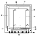
도 1은 종래의 유기전계발광 표시 장치를 설명하기 위한 평면도로서, 기판(10)의 화소 영역(20)에는 주사 라인(scan line)(22) 및 데이터 라인(data line)(24)과, 주사 라인(22) 및 데이터 라인(24) 사이에 매트릭스 방식으로 연결되어 화소를 구성하는 유기전계발광 소자(26)가 형성되고, 비화소 영역(30)에는 화소 영역(20)의 주사 라인(22) 및 데이터 라인(24)으로부터 연장된 주사 라인(22) 및 데이터 라인(24), 유기전계발광 소자(26)의 동작을 위한 전원 공급 라인(32 및 36) 그리고 패드부(40)를 통해 외부로부터 제공된 신호를 처리하여 주사 라인(22) 및 데이터 라인(24)으로 공급하는 주사 구동부(42) 및 데이터 구동부(44)가 형성된다. 상기와 같이 구성된 유기전계발광 표시 장치의 패드부(40)에는 필름 형태의 FPC(Flexible Printed Circuit; 도시안됨)가 전기적으로 접속되며, 외부로부터 FPC를 통해 신호(전원전압(ELVDD 및 ELVSS), 데이터 등)가 입력된다. 1 is a plan view illustrating a conventional organic light emitting display device. A scan line 22, a
패드부(40)를 통해 전원 공급 라인(32 및 36), 주사 구동부(42) 및 데이터 구동부(44)로 신호가 입력되면 주사 구동부(42) 및 데이터 구동부(44)는 주사 신호 및 데이터 신호를 각각 주사 라인(22) 및 데이터 라인(24)으로 공급한다. 따라서 주사 신호에 의해 선택된 화소의 유기전계발광 소자(26)가 데이터 신호에 상응하는 빛을 발광하게 된다.When a signal is input to the
그런데 종래의 유기전계발광 표시 장치는 외부로부터 전원전압(ELVDD 및 ELVSS)이 제공되는 패드부(40)가 도 2에 도시된 바와 같이 전원 공급 라인(32 및 36)의 일측부에 연결되기 때문에 연결부(A1 및 B1)로부터 각 유기전계발광 소자(26)까지의 거리가 다르다. 따라서 전압(V) 및 저항(R)이 하기의 수학식 1 및 수학식 2와 같이 표현될 때 전류(I) 및 단면적(A)이 일정하다고 가정하면, 패드부(40)로 입력된 전원전압(ELVDD 및 ELVSS)이 전원 공급 라인(32 및 36)으로 전달되는 연결부(A1 및 B1)로부터 유기전계발광 소자(26)까지의 거리(l)가 멀수록 전원 공급 라인(32 및 36)의 저항값(R)이 증가하기 때문에 하기의 수학식 3과 같이 전 압(V) 강하가 발생한다. However, in the conventional organic light emitting display device, since the
![]()
![]()


그러므로 전압 강하에 의해 유기전계발광 소자(26) 마다의 휘도 차이가 발생되어 화질이 불균일해지고, 캐소드 스위프(sweep)를 위해 캐소드(cathod) 전극에 전원전압(ELVSS)이 인가될 때 휘도 감소에 소요되는 시간의 차이가 발생한다. Therefore, the luminance drop is generated for each organic
본 발명의 목적은 전압 강하가 최소화될 수 있는 유기전계발광 표시 장치를 제공하는 데 있다.An object of the present invention is to provide an organic light emitting display device which can minimize the voltage drop.
상기한 목적을 달성하기 위한 본 발명의 일 측면에 따른 유기전계발광 표시 장치는 기판, 상기 기판 상에 형성된 다수의 제 1 라인 및 제 2 라인, 상기 기판 상에 형성되며 신호를 입력받기 위한 패드부, 상기 기판의 화소 영역에 형성되며, 상기 제 1 라인 및 제 2 라인 사이에 연결된 다수의 유기전계발광 소자, 상기 패드부와 상기 제 1 라인 사이에 연결된 제 1 구동부, 상기 패드부와 상기 제 2 라인 사이에 연결된 제 2 구동부, 상기 패드부와 상기 유기전계발광 소자 사이에 연결된 제 1 및 제 2 전원 공급 라인을 포함하며, 상기 패드부와 상기 제 1 전원 공급 라인의 연결부로부터 첫번째 상기 제 1 라인과 첫번째 상기 제 2 라인 사이에 연결된 유기전계발광 소자 및 상기 첫번째 제 1 라인과 마지막 상기 제 2 라인 사이에 연결된 유기전계발광 소자까지의 상기 제 1 전원 공급 라인의 길이가 동일하게 형성된 것을 특징으로 한다.An organic light emitting display device according to an aspect of the present invention for achieving the above object is a substrate, a plurality of first and second lines formed on the substrate, a pad unit formed on the substrate and receiving a signal A plurality of organic light emitting diodes formed in a pixel area of the substrate and connected between the first and second lines, a first driver connected between the pad and the first line, the pad and the second line A second driving part connected between the lines, first and second power supply lines connected between the pad part and the organic light emitting device, the first first line being connected to the pad part and the first power supply line; And an organic electroluminescent device connected between the first and second lines and an organic electroluminescent device connected between the first first line and the last second line. The length of the first power supply line is the same.
그러면 이하, 첨부된 도면을 참조하여 본 발명의 바람직한 실시예를 상세히 설명하기로 한다. 이하의 실시예는 이 기술 분야에서 통상적인 지식을 가진 자에게 본 발명이 충분히 이해되도록 제공되는 것으로서, 여러 가지 형태로 변형될 수 있으며, 본 발명의 범위가 다음에 기술되는 실시예에 한정되는 것은 아니다.Hereinafter, exemplary embodiments of the present invention will be described in detail with reference to the accompanying drawings. The following embodiments are provided to those skilled in the art to fully understand the present invention, and may be modified in various forms, and the scope of the present invention is limited to the embodiments described below. no.
도 3은 본 발명의 실시예에 따른 유기전계발광 표시 장치를 설명하기 위한 평면도이다.3 is a plan view illustrating an organic light emitting display device according to an exemplary embodiment of the present invention.
기판(100)의 화소 영역(120)에는 주사 라인(122) 및 데이터 라인(124)과, 주사 라인(122) 및 데이터 라인(124) 사이에 매트릭스 방식으로 연결되어 화소를 구성하는 유기전계발광 소자(126)가 형성되고, 비화소 영역(130)에는 화소 영역(120) 의 주사 라인(122) 및 데이터 라인(124)으로부터 연장된 주사 라인(122) 및 데이터 라인(124), 유기전계발광 소자(126)의 동작을 위한 전원 공급 라인(132 및 136) 그리고 패드부(140)를 통해 외부로부터 제공된 신호를 처리하여 주사 라인(122) 및 데이터 라인(124)으로 공급하는 주사 구동부(142) 및 데이터 구동부(144)가 형성된다. In the
유기전계발광 소자(126)는 애노드 전극 및 캐소드 전극과, 애노드 전극 및 캐소드 전극 사이에 형성된 유기 박막층으로 구성되며, 애노드 전극과 캐소드 전극에 소정의 전압이 인가되면 애노드 전극을 통해 주입되는 정공과 캐소드 전극을 통해 주입되는 전자가 유기 박막층에서 재결합하게 되고, 이 과정에서 발생되는 에너지 차이에 의해 빛을 방출한다. 유기 박막층은 정공 수송층, 유기 발광층 및 전자 수송층이 적층된 구조로 형성되거나, 정공 주입층과 전자 주입층이 더 포함될 수 있다. The organic
패시브 매트릭스(passive matrix) 방식의 경우 주사 라인(122) 및 데이터 라인(124) 사이에 유기전계발광 소자(126)가 매트릭스 방식으로 연결되고, 액티브 매트릭스(active matrix) 방식의 경우 주사 라인(122) 및 데이터 라인(124) 사이에 유기전계발광 소자(126)가 매트릭스 방식으로 연결되며, 유기전계발광 소자(126)의 동작을 제어하기 위한 박막 트랜지스터(Thin Film Transistor; TFT) 및 신호를 유지시키기 위한 캐패시터(capacitor)가 더 포함된다. In the case of the passive matrix method, the organic
주사 구동부(142) 및 데이터 구동부(144)는 유기전계발광 소자(126)의 제조 과정에서 비화소 영역(130)의 기판(100) 상에 형성되거나, 별도의 집적회로 반도체 칩(chip)으로 제조된 후 칩 온 글라스(Chip On Glass) 또는 와이어 본딩(wire bonding) 방법 등으로 주사 라인(122) 및 데이터 라인(124)과 연결되도록 기판(100)에 부착될 수 있다.The scan driver 142 and the
도 4는 유기전계발광 소자(126)를 보다 상세하게 설명하기 위한 단면도로서, 액티브 매트릭스 방식으로 구성된 일 예를 개략적으로 도시한다.4 is a cross-sectional view for describing the organic light
기판(100) 상에 버퍼층(101)이 형성되고, 버퍼층(101) 상에 활성층을 제공하는 반도체층(102)이 형성된다. 반도체층(102)은 박막 트랜지스터의 소스 및 드레인 영역(102a 및 102b)과 채널 영역(102c)을 제공한다. 반도체층(102)을 포함하는 전체 상부면에 게이트 절연막(103)이 형성되고, 반도체층(102) 상부의 게이트 절연막(103) 상에 게이트 전극(104)이 형성된다. 게이트 전극(104)을 포함하는 전체 상부면에 층간 절연막(105)이 형성되며, 층간 절연막(105)과 게이트 절연막(103)에는 반도체층(102)의 소스 및 드레인 영역(102a 및 102b)이 노출되도록 콘택홀이 형성된다. 층간 절연막(105) 상에는 콘택홀을 통해 소스 및 드레인 영역(102a 및 102b)과 연결되는 소스 및 드레인 전극(106a 및 106b)이 형성되고, 소스 및 드레인 전극(106a 및 106b)을 포함하는 전체 상부면에는 평탄화층(107)이 형성된다. 평탄화층(107)에는 소스 또는 드레인 전극(106a 또는 106b)이 노출되도록 비아홀이 형성되고, 평탄화층(107) 상에는 비아홀을 통해 소스 또는 드레인 전극(106a 또는 106b)과 연결되는 애노드 전극(108)이 형성된다. 또한, 평탄화층(107) 상에는 발광 영역의 애노드 전극(108)을 노출시키기 위한 화소 정의막(109)이 형성되고, 노출된 부분의 애노드 전극(108) 상에는 유기 박막층(110) 및 캐소드 전극(111)이 형성된 다. A
도 5는 패드부(140)를 통해 외부로부터 전원전압(ELVDD 및 ELVSS)이 제공되는 전원 공급 라인(132 및 136)을 보다 상세히 설명하기 위한 평면도이다. FIG. 5 is a plan view for describing in detail the
전원 공급 라인(132)은 화소 영역(120)의 적어도 일측에 형성되며 패드부(140)와 연결된 제 1 전원 버스 라인(132a)과, 제 1 전원 버스 라인(132a)으로부터 분배되어 화소 영역(120)의 유기전계발광 소자(126)와 연결된 다수의 제 2 전원 버스 라인(132b)으로 이루어진다. 이 때 전원 공급 라인(132)과 패드부(140)의 연결부(A2)는 제 1 전원 버스 라인(132a)의 중간부 즉, 첫번째 주사 라인(122)과 첫번째 데이터 라인(124) 사이에 연결된 유기전계발광 소자(126) 및 첫번째 주사 라인(122)과 마지막 데이터 라인(124) 사이에 연결된 유기전계발광 소자(126)까지의 전원 공급 라인(132)의 길이가 동일해지는 부분에 형성된다.The
전원 공급 라인(136)은 화소 영역(120)의 적어도 일측에 형성되며 패드부(140)와 연결된 제 1 전원 버스 라인(136a)과, 제 1 전원 버스 라인(136a)과 연결되며 화소 영역(120)의 다른 일측 또는 화소 영역(120)을 둘러싸도록 형성된 제 2 전원 버스 라인(136b)으로 이루어진다. 전원 공급 라인(136)의 상부에는 유기전계발광 소자(126)의 캐소드 전극(111)이 형성되어 전원 공급 라인(136)을 통해 캐소드 전극(111)으로 전원전압(ELVSS)이 인가될 수 있다. 전원 공급 라인(132)과 패드부(140)의 연결부(B2)는 전원 공급 라인(132)과 비대칭으로 형성되는데, 예를 들어, 제 1 전원 버스 라인(132a)과 패드부(140)의 연결부(A2)와 인접된 제 1 전원 버스 라인(136a)의 일측부에 형성될 수 있다. The
상기 실시예에서 면저항값이 감소되도록 제 1 전원 버스 라인(132a 및 136a)이 제 2 전원 버스 라인(132b 및 136b)보다 넓게 형성되는 것이 바람직하다. 또한, 패드부(140)에서 연결부(A2 및 B2)까지의 거리와 제 1 전원 버스 라인(132a)에서 각 유기전계발광 소자(126)까지의 제 2 전원 버스 라인(132b)의 길이도 최단 거리로 설계되는 것이 바람직하다. 상기 실시예에 따르면, 패드부(140)에서 연결부(A2 및 B2)까지의 거리는 종래의 경우보다 증가될 수 있지만, 이에 따른 소비전력의 증가는 1% 미만이므로 무시해도 된다. In the above embodiment, it is preferable that the first
상기와 같이 구성된 유기전계발광 표시 장치의 패드부(140)에는 필름 형태의 FPC(도시안됨)가 전기적으로 접속되며, 외부로부터 FPC를 통해 신호(전원전압(ELVDD 및 ELVSS), 데이터 등)가 입력된다. 패드부(140)를 통해 전원 공급 라인(132 및 136), 주사 구동부(142) 및 데이터 구동부(144)로 신호가 입력되면 주사 구동부(142) 및 데이터 구동부(144)는 주사 신호 및 데이터 신호를 각각 주사 라인(122) 및 데이터 라인(124)으로 공급한다. 따라서 주사 신호에 의해 선택된 화소의 유기전계발광 소자(126)가 데이터 신호에 상응하는 빛을 발광하게 된다.A film-type FPC (not shown) is electrically connected to the
본 발명에 따르면 패드부(140)를 통해 입력된 전원전압(ELVDD)은 연결부(A2)를 통해 제 1 전원 버스 라인(132a)으로 전달된 후 제 2 전원 버스 라인(132b)을 통해 각 유기전계발광 소자(126)로 분배되는데, 연결부(A2)로부터 전원 전달 경로가 가장 긴 즉, 첫번째 주사 라인(122)과 첫번째 데이터 라인(124) 사이에 연결된 유기전계발광 소자(126) 및 첫번째 주사 라인(122)과 마지막 데이터 라인(124) 사이에 연결된 유기전계발광 소자(126)까지의 전원 공급 라인(132)의 길이가 동일하 기 때문에 각 유기전계발광 소자(126)에는 동일한 전원전압(ELVDD)이 인가된다.According to the present invention, the power supply voltage ELVDD input through the
또한, 패드부(140)를 통해 제공된 전원전압(ELVSS)은 연결부(B2)를 통해 제 1 전원 버스 라인(136a)으로 전달된 후 제 2 전원 버스 라인(136b)을 통해 각 유기전계발광 소자(126)로 분배되는데, 화소 영역(120)을 둘러싸도록 형성된 전원 공급 라인(136) 상부에 유기전계발광 소자(126)의 캐소드 전극(111)이 형성되기 때문에 첫번째 주사 라인(122)과 첫번째 데이터 라인(124) 사이에 연결된 유기전계발광 소자(126) 및 첫번째 주사 라인(122)과 마지막 데이터 라인(124) 사이에 연결된 유기전계발광 소자(126)까지의 전원 전달 경로의 길이가 동일하기 때문에 각 유기전계발광 소자(126)에는 동일한 전원전압(ELVSS)이 인가된다.In addition, the power supply voltage ELVSS provided through the
따라서 유기전계발광 소자의 휘도는 하기의 수학식 4와 같이 유기전계발광 소자를 통해 흐르는 전류(IOLED)의 량에 의해 결정되는데, 본 발명에 따르면 전원전압의 강하가 최소화되므로 유기전계발광 소자의 휘도 저하가 최소화될 수 있다.Therefore, the luminance of the organic light emitting diode is determined by the amount of current (I OLED ) flowing through the organic light emitting diode as shown in Equation 4 below. Luminance degradation can be minimized.

여기서, VGS는 구동 트랜지스터의 게이트 및 소스 간의 전압, Vth는 구동 트랜지스터의 문턱전압, VDATA는 데이터 전압 및 ρ는 상수이다.Here, V GS is a voltage between a gate and a source of the driving transistor, V th is a threshold voltage of the driving transistor, V DATA is a data voltage and ρ is a constant.
이상에서와 같이 상세한 설명과 도면을 통해 본 발명의 최적 실시예를 개시하였다. 용어들은 단지 본 발명을 설명하기 위한 목적에서 사용된 것이지 의미 한 정이나 특허청구범위에 기재된 본 발명의 범위를 제한하기 위하여 사용된 것은 아니다. 그러므로 본 기술 분야의 통상의 지식을 가진 자라면 이로부터 다양한 변형 및 균등한 타 실시예가 가능하다는 점을 이해할 것이다. 따라서 본 발명의 진정한 기술적 보호 범위는 첨부된 특허청구범위의 기술적 사상에 의해 정해져야 할 것이다.As described above, the preferred embodiment of the present invention has been disclosed through the detailed description and the drawings. The terms are used only for the purpose of describing the present invention and are not intended to limit the scope of the present invention as defined in the meaning or claims. Therefore, those skilled in the art will understand that various modifications and equivalent other embodiments are possible from this. Therefore, the true technical protection scope of the present invention will be defined by the technical spirit of the appended claims.
상술한 바와 같이 본 발명은 패드부를 통해 입력된 전원전압이 전원 공급 라인을 통해 화소 영역의 각 유기전계발광 소자로 공급될 때 패드부와 전원 공급 라인의 연결부로부터 각 유기전계발광 소자까지의 전원 공급 라인의 길이 차이로 인한 전압 강하가 최소화되도록 함으로써 균일한 휘도를 구현할 수 있다.As described above, in the present invention, when the power supply voltage input through the pad unit is supplied to each organic electroluminescent element in the pixel region through the power supply line, power is supplied from the connecting portion of the pad unit and the power supply line to each organic electroluminescent element. Uniform luminance can be achieved by minimizing the voltage drop due to the difference in line lengths.
Claims (8)
Priority Applications (1)
| Application Number | Priority Date | Filing Date | Title |
|---|---|---|---|
| KR1020060067392A KR100732811B1 (en) | 2006-07-19 | 2006-07-19 | Organic light emitting display device |
Applications Claiming Priority (1)
| Application Number | Priority Date | Filing Date | Title |
|---|---|---|---|
| KR1020060067392A KR100732811B1 (en) | 2006-07-19 | 2006-07-19 | Organic light emitting display device |
Publications (1)
| Publication Number | Publication Date |
|---|---|
| KR100732811B1 true KR100732811B1 (en) | 2007-06-27 |
Family
ID=38373556
Family Applications (1)
| Application Number | Title | Priority Date | Filing Date |
|---|---|---|---|
| KR1020060067392A Expired - Fee Related KR100732811B1 (en) | 2006-07-19 | 2006-07-19 | Organic light emitting display device |
Country Status (1)
| Country | Link |
|---|---|
| KR (1) | KR100732811B1 (en) |
Cited By (3)
| Publication number | Priority date | Publication date | Assignee | Title |
|---|---|---|---|---|
| US8432334B2 (en) | 2009-08-20 | 2013-04-30 | Samsung Display Co., Ltd. | Organic light emitting display device |
| US9443474B2 (en) | 2012-07-06 | 2016-09-13 | Samsung Display Co., Ltd. | Organic light emitting display apparatus and method of driving the same |
| CN110676298A (en) * | 2019-09-30 | 2020-01-10 | 昆山国显光电有限公司 | Array substrate and OLED display panel |
Citations (3)
| Publication number | Priority date | Publication date | Assignee | Title |
|---|---|---|---|---|
| JP2001109397A (en) | 1999-10-04 | 2001-04-20 | Sanyo Electric Co Ltd | El display device |
| KR20050072007A (en) * | 2004-01-05 | 2005-07-08 | 삼성에스디아이 주식회사 | Electro luminescence display panel |
| KR20060010355A (en) * | 2004-07-28 | 2006-02-02 | 삼성에스디아이 주식회사 | Light emitting display |
-
2006
- 2006-07-19 KR KR1020060067392A patent/KR100732811B1/en not_active Expired - Fee Related
Patent Citations (3)
| Publication number | Priority date | Publication date | Assignee | Title |
|---|---|---|---|---|
| JP2001109397A (en) | 1999-10-04 | 2001-04-20 | Sanyo Electric Co Ltd | El display device |
| KR20050072007A (en) * | 2004-01-05 | 2005-07-08 | 삼성에스디아이 주식회사 | Electro luminescence display panel |
| KR20060010355A (en) * | 2004-07-28 | 2006-02-02 | 삼성에스디아이 주식회사 | Light emitting display |
Cited By (3)
| Publication number | Priority date | Publication date | Assignee | Title |
|---|---|---|---|---|
| US8432334B2 (en) | 2009-08-20 | 2013-04-30 | Samsung Display Co., Ltd. | Organic light emitting display device |
| US9443474B2 (en) | 2012-07-06 | 2016-09-13 | Samsung Display Co., Ltd. | Organic light emitting display apparatus and method of driving the same |
| CN110676298A (en) * | 2019-09-30 | 2020-01-10 | 昆山国显光电有限公司 | Array substrate and OLED display panel |
Similar Documents
| Publication | Publication Date | Title |
|---|---|---|
| KR102600512B1 (en) | Display device | |
| US8004178B2 (en) | Organic light emitting diode display with a power line in a non-pixel region | |
| US8441420B2 (en) | Organic electroluminescent display device having plurality of driving transistors and plurality of anodes or cathodes per pixel | |
| KR101980757B1 (en) | Organic light-emitting diode display device | |
| JP4150012B2 (en) | Organic electroluminescence display panel | |
| KR100600332B1 (en) | Light emitting display | |
| US11410595B2 (en) | Display device and driving method for display device | |
| US8149230B2 (en) | Light emitting display | |
| KR101368006B1 (en) | Organic Light Emitting Display and Method of Driving the same | |
| CN101582439B (en) | Organic light emitting display and method for making the same | |
| CN110416254B (en) | Array substrate and display panel | |
| KR20200040952A (en) | Display device | |
| CN111354758B (en) | Light Emitting Diode Display Devices | |
| CN111435585A (en) | Organic light emitting diode display | |
| CN104751796A (en) | Organic light emitting display device | |
| KR102643466B1 (en) | Organic light emitting diode display device | |
| KR20220159560A (en) | Display device and manufacturing method of the same | |
| US11094774B2 (en) | Organic light emitting diode display device | |
| KR100732811B1 (en) | Organic light emitting display device | |
| US20190363150A1 (en) | Display device | |
| KR101493223B1 (en) | Organic light emitting display | |
| KR20060058515A (en) | Light emitting display device and manufacturing method thereof | |
| KR102013893B1 (en) | Flat panel display device and method for fabricating the same | |
| US20250280675A1 (en) | Light Emitting Display Apparatus | |
| KR100599772B1 (en) | Organic electro luminescent display panel |
Legal Events
| Date | Code | Title | Description |
|---|---|---|---|
| A201 | Request for examination | ||
| PA0109 | Patent application |
St.27 status event code: A-0-1-A10-A12-nap-PA0109 |
|
| PA0201 | Request for examination |
St.27 status event code: A-1-2-D10-D11-exm-PA0201 |
|
| D13-X000 | Search requested |
St.27 status event code: A-1-2-D10-D13-srh-X000 |
|
| D14-X000 | Search report completed |
St.27 status event code: A-1-2-D10-D14-srh-X000 |
|
| E701 | Decision to grant or registration of patent right | ||
| PE0701 | Decision of registration |
St.27 status event code: A-1-2-D10-D22-exm-PE0701 |
|
| GRNT | Written decision to grant | ||
| PR0701 | Registration of establishment |
St.27 status event code: A-2-4-F10-F11-exm-PR0701 |
|
| PR1002 | Payment of registration fee |
St.27 status event code: A-2-2-U10-U11-oth-PR1002 Fee payment year number: 1 |
|
| PG1601 | Publication of registration |
St.27 status event code: A-4-4-Q10-Q13-nap-PG1601 |
|
| PN2301 | Change of applicant |
St.27 status event code: A-5-5-R10-R11-asn-PN2301 |
|
| R18-X000 | Changes to party contact information recorded |
St.27 status event code: A-5-5-R10-R18-oth-X000 |
|
| R18-X000 | Changes to party contact information recorded |
St.27 status event code: A-5-5-R10-R18-oth-X000 |
|
| R18-X000 | Changes to party contact information recorded |
St.27 status event code: A-5-5-R10-R18-oth-X000 |
|
| PR1001 | Payment of annual fee |
St.27 status event code: A-4-4-U10-U11-oth-PR1001 Fee payment year number: 4 |
|
| PR1001 | Payment of annual fee |
St.27 status event code: A-4-4-U10-U11-oth-PR1001 Fee payment year number: 5 |
|
| PR1001 | Payment of annual fee |
St.27 status event code: A-4-4-U10-U11-oth-PR1001 Fee payment year number: 6 |
|
| PN2301 | Change of applicant |
St.27 status event code: A-5-5-R10-R11-asn-PN2301 |
|
| PN2301 | Change of applicant |
St.27 status event code: A-5-5-R10-R14-asn-PN2301 |
|
| FPAY | Annual fee payment |
Payment date: 20130530 Year of fee payment: 7 |
|
| PR1001 | Payment of annual fee |
St.27 status event code: A-4-4-U10-U11-oth-PR1001 Fee payment year number: 7 |
|
| R18-X000 | Changes to party contact information recorded |
St.27 status event code: A-5-5-R10-R18-oth-X000 |
|
| FPAY | Annual fee payment |
Payment date: 20140530 Year of fee payment: 8 |
|
| PR1001 | Payment of annual fee |
St.27 status event code: A-4-4-U10-U11-oth-PR1001 Fee payment year number: 8 |
|
| FPAY | Annual fee payment |
Payment date: 20150601 Year of fee payment: 9 |
|
| PR1001 | Payment of annual fee |
St.27 status event code: A-4-4-U10-U11-oth-PR1001 Fee payment year number: 9 |
|
| R18-X000 | Changes to party contact information recorded |
St.27 status event code: A-5-5-R10-R18-oth-X000 |
|
| LAPS | Lapse due to unpaid annual fee | ||
| PC1903 | Unpaid annual fee |
St.27 status event code: A-4-4-U10-U13-oth-PC1903 Not in force date: 20160621 Payment event data comment text: Termination Category : DEFAULT_OF_REGISTRATION_FEE |
|
| P22-X000 | Classification modified |
St.27 status event code: A-4-4-P10-P22-nap-X000 |
|
| PC1903 | Unpaid annual fee |
St.27 status event code: N-4-6-H10-H13-oth-PC1903 Ip right cessation event data comment text: Termination Category : DEFAULT_OF_REGISTRATION_FEE Not in force date: 20160621 |
|
| R18-X000 | Changes to party contact information recorded |
St.27 status event code: A-5-5-R10-R18-oth-X000 |
|
| P22-X000 | Classification modified |
St.27 status event code: A-4-4-P10-P22-nap-X000 |