KR100625944B1 - Photodiode of CMOS image sensor and its manufacturing method - Google Patents
Photodiode of CMOS image sensor and its manufacturing method Download PDFInfo
- Publication number
- KR100625944B1 KR100625944B1 KR1020050058459A KR20050058459A KR100625944B1 KR 100625944 B1 KR100625944 B1 KR 100625944B1 KR 1020050058459 A KR1020050058459 A KR 1020050058459A KR 20050058459 A KR20050058459 A KR 20050058459A KR 100625944 B1 KR100625944 B1 KR 100625944B1
- Authority
- KR
- South Korea
- Prior art keywords
- silicon germanium
- silicon
- image sensor
- cmos image
- epitaxial layer
- Prior art date
- Legal status (The legal status is an assumption and is not a legal conclusion. Google has not performed a legal analysis and makes no representation as to the accuracy of the status listed.)
- Expired - Fee Related
Links
Images


Classifications
-
- H—ELECTRICITY
- H10—SEMICONDUCTOR DEVICES; ELECTRIC SOLID-STATE DEVICES NOT OTHERWISE PROVIDED FOR
- H10F—INORGANIC SEMICONDUCTOR DEVICES SENSITIVE TO INFRARED RADIATION, LIGHT, ELECTROMAGNETIC RADIATION OF SHORTER WAVELENGTH OR CORPUSCULAR RADIATION
- H10F39/00—Integrated devices, or assemblies of multiple devices, comprising at least one element covered by group H10F30/00, e.g. radiation detectors comprising photodiode arrays
- H10F39/10—Integrated devices
- H10F39/12—Image sensors
-
- H—ELECTRICITY
- H10—SEMICONDUCTOR DEVICES; ELECTRIC SOLID-STATE DEVICES NOT OTHERWISE PROVIDED FOR
- H10F—INORGANIC SEMICONDUCTOR DEVICES SENSITIVE TO INFRARED RADIATION, LIGHT, ELECTROMAGNETIC RADIATION OF SHORTER WAVELENGTH OR CORPUSCULAR RADIATION
- H10F39/00—Integrated devices, or assemblies of multiple devices, comprising at least one element covered by group H10F30/00, e.g. radiation detectors comprising photodiode arrays
- H10F39/80—Constructional details of image sensors
- H10F39/803—Pixels having integrated switching, control, storage or amplification elements
-
- H—ELECTRICITY
- H10—SEMICONDUCTOR DEVICES; ELECTRIC SOLID-STATE DEVICES NOT OTHERWISE PROVIDED FOR
- H10F—INORGANIC SEMICONDUCTOR DEVICES SENSITIVE TO INFRARED RADIATION, LIGHT, ELECTROMAGNETIC RADIATION OF SHORTER WAVELENGTH OR CORPUSCULAR RADIATION
- H10F39/00—Integrated devices, or assemblies of multiple devices, comprising at least one element covered by group H10F30/00, e.g. radiation detectors comprising photodiode arrays
- H10F39/011—Manufacture or treatment of image sensors covered by group H10F39/12
- H10F39/014—Manufacture or treatment of image sensors covered by group H10F39/12 of CMOS image sensors
-
- H—ELECTRICITY
- H10—SEMICONDUCTOR DEVICES; ELECTRIC SOLID-STATE DEVICES NOT OTHERWISE PROVIDED FOR
- H10F—INORGANIC SEMICONDUCTOR DEVICES SENSITIVE TO INFRARED RADIATION, LIGHT, ELECTROMAGNETIC RADIATION OF SHORTER WAVELENGTH OR CORPUSCULAR RADIATION
- H10F39/00—Integrated devices, or assemblies of multiple devices, comprising at least one element covered by group H10F30/00, e.g. radiation detectors comprising photodiode arrays
- H10F39/10—Integrated devices
- H10F39/12—Image sensors
- H10F39/18—Complementary metal-oxide-semiconductor [CMOS] image sensors; Photodiode array image sensors
-
- H—ELECTRICITY
- H10—SEMICONDUCTOR DEVICES; ELECTRIC SOLID-STATE DEVICES NOT OTHERWISE PROVIDED FOR
- H10F—INORGANIC SEMICONDUCTOR DEVICES SENSITIVE TO INFRARED RADIATION, LIGHT, ELECTROMAGNETIC RADIATION OF SHORTER WAVELENGTH OR CORPUSCULAR RADIATION
- H10F39/00—Integrated devices, or assemblies of multiple devices, comprising at least one element covered by group H10F30/00, e.g. radiation detectors comprising photodiode arrays
- H10F39/80—Constructional details of image sensors
-
- H—ELECTRICITY
- H10—SEMICONDUCTOR DEVICES; ELECTRIC SOLID-STATE DEVICES NOT OTHERWISE PROVIDED FOR
- H10F—INORGANIC SEMICONDUCTOR DEVICES SENSITIVE TO INFRARED RADIATION, LIGHT, ELECTROMAGNETIC RADIATION OF SHORTER WAVELENGTH OR CORPUSCULAR RADIATION
- H10F77/00—Constructional details of devices covered by this subclass
- H10F77/10—Semiconductor bodies
- H10F77/14—Shape of semiconductor bodies; Shapes, relative sizes or dispositions of semiconductor regions within semiconductor bodies
Landscapes
- Solid State Image Pick-Up Elements (AREA)
- Light Receiving Elements (AREA)
Abstract
본 발명은 포토다이오드의 전자홀쌍 생성률을 증가시켜 노이즈에 대한 저항성이 높은 씨모스 이미지 센서 및 그의 제조 방법을 제공하기 위한 것으로, 본 발명의 씨모스 이미지 센서의 제조 방법은 실리콘기판 상에 에피택시 공정을 통해 소정 농도의 불순물이 도핑된 실리콘저마늄에피층을 성장시키는 단계, 상기 실리콘저마늄에피층 상에 에피택시 공정을 통해 언도우프드 실리콘에피층을 성장시키는 단계, 및 이온주입을 통해 상기 언도우프드 실리콘에피층의 표면으로부터 상기 실리콘저마늄에피층의 일부까지의 소정 깊이로 포토다이오드영역을 형성하는 단계를 포함하고, 이와 같은 본 발명의 씨모스 이미지 센서는, 포토다이오드영역이 형성되는 부분이 실리콘저마늄에피층이므로 실리콘에피층에 형성된 포토다이오드보다 높은 양자효율(Quantum efficiency)이 확보되어 동일한 광자에 대해서 더 많은 전자홀쌍이 생성되어 높은 감도를 구현할 수 있다.The present invention is to provide a CMOS image sensor having a high resistance to noise by increasing the electron-hole pair generation rate of the photodiode and a manufacturing method thereof, the manufacturing method of the CMOS image sensor of the present invention is an epitaxy process on a silicon substrate Growing a silicon germanium epi layer doped with a predetermined concentration of impurities through the epitaxial process on the silicon germanium epi layer, and implanting the undoped silicon epi layer through ion implantation And forming a photodiode region at a predetermined depth from the surface of the woven silicon epitaxial layer to a portion of the silicon germanium epitaxial layer, wherein the CMOS image sensor of the present invention comprises a portion where the photodiode region is formed. Since this silicon germanium epi layer is higher than the photodiode formed on the silicon epi layer, um efficiency can be ensured that more electron hole pairs can be generated for the same photon, thereby achieving high sensitivity.
씨모스 이미지 센서, 포토다이오드, 감도, 실리콘저마늄에피층, 실리콘에피층 CMOS image sensor, photodiode, sensitivity, silicon germanium epi layer, silicon epi layer
Description
도 1은 종래기술에 따른 씨모스 이미지 센서의 구조를 도시한 도면,1 is a view showing the structure of a CMOS image sensor according to the prior art,
도 2는 본 발명의 실시예에 따른 씨모스 이미지 센서의 구조를 도시한 도면,2 is a diagram illustrating a structure of a CMOS image sensor according to an exemplary embodiment of the present invention;
도 3a 내지 도 3f는 본 발명의 실시예에 따른 씨모스 이미지 센서의 제조 방법을 도시한 공정 단면도.3A to 3F are cross-sectional views illustrating a method of manufacturing the CMOS image sensor according to an exemplary embodiment of the present invention.
* 도면의 주요 부분에 대한 부호의 설명* Explanation of symbols for the main parts of the drawings
21 : 실리콘기판 22 : 제1실리콘저마늄에피층21
23 : 제2실리콘저마늄에피층 24 : 제3실리콘저마늄에피층23: 2nd silicon germanium epi layer 24: 3rd silicon germanium epi layer
25 : 언도우프드 실리콘에피층 30 : 포토다이오드 영역25 undoped silicon
100 : 실리콘저마늄에피층100: silicon germanium epi layer
본 발명은 이미지 센서에 관하 것으로, 특히 씨모스 이미지 센서 및 그의 제조 방법에 관한 것이다.TECHNICAL FIELD The present invention relates to an image sensor, and more particularly, to a CMOS image sensor and a manufacturing method thereof.
일반적으로 이미지센서(Image sensor)는 반도체 물질이 빛에 반응하는 성질을 이용하여 영상정보를 캡쳐하는 장치로서, 빛의 밝기 및 파장 등이 다른 피사체를 감지하는 각 화소(Pixel)에서 다르게 나타나는 전기적 값을 신호처리가 가능한 레벨로 만들어 주는 장치를 일컫는다. In general, an image sensor is an apparatus for capturing image information by using a property of a semiconductor material reacting to light, and an electrical value that is different from each pixel that senses a different object such as brightness and wavelength of light. Refers to a device that makes the signal processing level possible.
이러한 이미지센서에는 CCD(Charged Coupled Device) 이미지센서와 씨모스이미지센서(CMOS Image sensor)가 있으며, 외부의 피사체영상을 촬상한 빛을 흡수하여 광전하를 모으고 축적하는 수광소자로 포토다이오드(Photodiode; PD)를 이용한다.Such an image sensor includes a Charged Coupled Device (CCD) image sensor and a CMOS image sensor. A photodiode is a light-receiving element that absorbs and captures photoelectric charges by capturing an external subject image. PD).
통상적인 씨모스 이미지센서의 단위화소(Unit Pixel)는 하나의 포토다이오드(Photodiode; PD)와 네 개의 NMOS(Tx,Rx,Sx,Dx)로 구성되며, 네 개의 NMOS(Tx,Rx,Sx,Dx)는 포토다이오드(PD)에서 집속된 광전하(Photo-generated charge)를 플로팅디퓨젼영역(Floating Diffusion; FD)으로 운송하기 위한 트랜스퍼트랜지스터(Transfer transistor; Tx), 원하는 값으로 노드의 전위를 세팅하고 전하(Cpd)를 배출하여 플로팅디퓨젼영역(FD)을 리셋(Reset)시키기 위한 리셋트랜지스터(Reset transistor; Rx), 소오스팔로워-버퍼증폭기(Source Follower Buffer Amplif ier) 역할을 하는 드라이브트랜지스터(Drive transistor; Dx), 스위칭으로 어드레싱(Addressing)을 할 수 있도록 하는 셀렉트트랜지스터(Select transistor; Sx)로 구성된다. 여기서 트랜스퍼트랜지스터(Tx) 및 리셋트랜지스터(Rx)는 네이티브트랜지스터(Native NMOS)를 이용하고 드라이브트랜지스터(Dx) 및 셀렉트트랜지스터(Sx)는 일반적인 트랜지스터(Normal NMOS)를 이용하며, 리셋트랜지스터(Rx)는 CDS(Correlated Double Sampling)를 위한 트랜지스터이다.The unit pixel of a conventional CMOS image sensor is composed of one photodiode (PD) and four NMOS (Tx, Rx, Sx, Dx), and four NMOS (Tx, Rx, Sx, Dx) is a transfer transistor (Tx) for transporting photo-generated charges concentrated in the photodiode (PD) to the floating diffusion region (FD), and the potential of the node to a desired value. A reset transistor (Rx) and a drive transistor acting as a source follower buffer amplifier to reset the floating diffusion region (FD) by setting and discharging the charge (C pd ). (Drive transistor; Dx), and a select transistor (Sx) for addressing (Addressing) by switching. Here, the transfer transistor (Tx) and the reset transistor (Rx) use a native transistor (Native NMOS), the drive transistor (Dx) and the select transistor (Sx) use a common transistor (Normal NMOS), and the reset transistor (Rx) A transistor for correlated double sampling (CDS).
상기와 같은 씨모스이미지센서의 단위화소(Unit Pixel)는 네이티브트랜지스터(Native Transistor)를 사용하여 포토다이오드(PD)에서 가시광선파장대역의 광을 감지한 후 감지된 광전하(Photogenerated charge)를 플로우팅디퓨전영역(FD)으로, 즉 드라이브트랜지스터(Dx)의 게이트로 전달한 양을 출력단(Vout)에서 전기적신호로 출력한다.The unit pixel of the CMOS image sensor flows the detected photogenerated charge after detecting the light of the visible wavelength band from the photodiode using a native transistor. The amount transferred to the TD diffusion region FD, that is, the gate of the drive transistor Dx, is output as an electrical signal at the output terminal Vout.
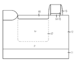
도 1은 종래기술에 따른 씨모스 이미지 센서의 구조를 도시한 도면으로서, 포토다이오드와 트랜스퍼트랜지스터만을 도시하고 있다.1 is a view illustrating a structure of a CMOS image sensor according to the related art, and illustrates only a photodiode and a transfer transistor.
도 1에 도시된 바와 같이, p형 불순물이 고농도로 도핑된 p++ 기판(11)에 p형 불순물이 인시튜로 도핑되어 에피택셜 성장된 p형 에피층(12)이 형성되고, p형 에피층(12)의 일부분에에 소자간 격리를 위한 필드산화막(13)이 형성된다.As shown in FIG. 1, a p-type impurity is doped in situ on a p ++ substrate 11 doped with a high concentration of p-type impurities to form an epitaxially grown p-type
그리고, p형 에피층(12)의 일측 표면 상에 게이트산화막(14)이 형성되고, 게이트산화막(14) 상에 트랜스퍼트랜지스터(Tx)의 게이트전극(15)이 형성되며, 게이트산화막(14)과 게이트전극(15)의 양측벽에 스페이서(16)가 형성되어 있다.The
그리고, 게이트전극(15)의 일측벽의 스페이서(16) 에지에 정렬되면서 p 형 에피층(12) 내부에 소정 깊이를 갖는 n형 불순물영역(17)이 형성되고, n형 불순물 영역(17) 상부와 p형 에피층(12)의 표면 하부에 스페이서(17)에 정렬되는 p형 불순물영역(18)이 형성된다. 여기서, n형 불순물 영역(17)은 깊은 n- 영역이라 일컫고, p형 불순물 영역(18)은 p0 영역이라고 일컫는다.Then, an n-
도 1의 종래기술은 n형 불순물영역(17)과 p형 에피층(12)으로 이루어진 PN 접합 부근에서 광에 의한 전자-홀 페어(Electron-Hole Pair; EHP) 캐리어들이 발생하고, 이 캐리어들이 인가된 바이어스에 의해 트랜지스퍼트랜지스터(Tx)로 이동하여 전류를 발생하므로서 광에너지를 전류로 전환한다.In the prior art of FIG. 1, electron-hole pair (EHP) carriers by light are generated in the vicinity of a PN junction composed of an n-
결국, n형 불순물 영역(17)과 p형 에피층(12)으로 이루어진 pn 접합이 포토다이오드가 된다.As a result, a pn junction composed of the n-
그러가, 종래기술의 포토다이오드는 기본적으로 실리콘(p형 에피층과 n형 불순물영역이 모두 실리콘물질)을 매질로 하기 때문에 광에너지 입사시 전자홀쌍(EHP) 생성률(Generation rate)이 떨어져 낮은 전류를 발생한다. 이러한 특성은 노이즈(Noise)에 대한 저항성을 저하시킨다.However, since the photodiode of the prior art basically uses silicon (both p-type epi layer and n-type impurity region as a silicon material), a low current due to the generation rate of electron hole pair (EHP) is low when light energy is incident. Occurs. This property lowers the resistance to noise.
본 발명은 상기한 종래기술의 문제점을 해결하기 위해 제안된 것으로, 포토다이오드의 전자홀쌍 생성률을 증가시켜 노이즈에 대한 저항성이 높은 씨모스 이미지 센서 및 그의 제조 방법을 제공하는데 그 목적이 있다.The present invention has been proposed to solve the above problems of the prior art, and an object thereof is to provide a CMOS image sensor having high resistance to noise and a method of manufacturing the same by increasing the electron hole pair generation rate of the photodiode.
상기 목적을 달성하기 위한 본 발명의 씨모스 이미지 센서는 실리콘기판, 상기 실리콘기판 상에 에피택시 공정을 통해 성장되고 소정 농도의 불순물이 도핑된 실리콘저마늄에피층, 상기 실리콘저마늄에피층 상에 에피택시 공정을 통해 성장된 언도우프드 실리콘에피층, 및 상기 언도우프드 실리콘에피층의 표면으로부터 상기 실리콘저마늄에피층의 일부까지의 소정 깊이로 형성된 포토다이오드영역을 포함하는 것을 특징으로 하고, 상기 실리콘저마늄에피층은 저마늄농도가 점진적으로 증가하는 도핑프로파일을 갖는 제1실리콘저마늄에피층, 상기 제1실리콘저마늄에피층 상에 성장되며 고농도의 p형 불순물이 도핑된 제2실리콘저마늄에피층, 및 상기 제2실리콘저마늄에피층 상에 성장되며 저농도의 p형 불순물이 도핑된 제3실리콘저마늄에피층을 포함하는 것을 특징으로 하며, 상기 제1실리콘저마늄에피층은 저마늄농도가 0%∼20%까지 점진적으로 증가되고, 상기 제2 및 제3실리콘저마늄에피층의 저마늄농도는 20% 수준으로 일정하게 유지되는 것을 특징으로 하고, 상기 제2 및 제3실리콘저마늄에피층에 도핑된 p형 불순물은 보론이고, 상기 제2실리콘저마늄에피층에 도핑된 보론의 농도는 1E15/cm3∼1E18/cm3이며, 상기 제3실리콘저마늄에피층에 도핑된 보론의 농도는 1E14/cm3∼1E17/cm3인 것을 특징으로 한다.The CMOS image sensor of the present invention for achieving the above object is a silicon germanium epitaxial layer on the silicon substrate, the silicon germanium epi layer doped with a predetermined concentration of impurities and grown on the silicon substrate through the epitaxial process, on the silicon germanium epi layer An undoped silicon epi layer grown through an epitaxy process, and a photodiode region formed at a predetermined depth from a surface of the undoped silicon epi layer to a portion of the silicon germanium epi layer, The silicon germanium epitaxial layer is grown on a first silicon germanium epitaxial layer having a doping profile in which germanium concentration is gradually increased, and a second silicon doped with a high concentration of p-type impurities. A third silicon germanium epi layer grown on the germanium epi layer and the second silicon germanium epi layer and doped with a low concentration of p-type impurities. The first silicon germanium epi layer is gradually increased from 0% to 20% germanium concentration, the germanium concentration of the second and third silicon germanium epi layer to 20% level. The p-type impurities doped in the second and third silicon germanium epitaxial layers are boron, and the concentration of boron doped in the second silicon germanium epitaxial layer is 1E15 / cm 3- . 1E18 / cm 3 and the concentration of boron doped in the third silicon germanium epi layer is characterized in that 1E14 / cm 3 ~ 1E17 / cm 3 .
그리고, 본 발명의 씨모스 이미지 센서의 제조 방법은 실리콘기판 상에 에피택시 공정을 통해 소정 농도의 불순물이 도핑된 실리콘저마늄에피층을 성장시키는 단계, 상기 실리콘저마늄에피층 상에 에피택시 공정을 통해 언도우프드 실리콘에피 층을 성장시키는 단계, 및 이온주입을 통해 상기 언도우프드 실리콘에피층의 표면으로부터 상기 실리콘저마늄에피층의 일부까지의 소정 깊이로 포토다이오드영역을 형성하는 단계를 포함하는 것을 특징으로 하고, 상기 실리콘저마늄에피층을 성장시키는 단계는 저마늄농도가 점진적으로 증가하는 도핑프로파일을 갖는 제1실리콘저마늄에피층을 성장시키는 단계, 어닐을 실시하여 상기 제1실리콘저마늄에피층에 생성된 스트레스를 해소시키는 단계, 상기 어닐이 실시된 제1실리콘저마늄에피층 상에 고농도의 p형 불순물이 도핑된 제2실리콘저마늄에피층을 성장시키는 단계, 및 상기 제2실리콘저마늄에피층 상에 저농도의 p형 불순물이 도핑된 제3실리콘저마늄에피층을 성장시키는 단계를 포함하고, 상기 포토다이오드영역은 상기 언도우프드 실리콘에피층의 표면으로부터 상기 제3실리콘저마늄에피층의 일부까지의 깊이로 형성하는 것을 특징으로 하며, 상기 제1실리콘저마늄에피층은 성장도중에 저마늄농도가 0%∼20%까지 점진적으로 증가되고, 상기 제2 및 제3실리콘저마늄에피층의 저마늄농도는 20% 수준으로 일정하게 유지되는 것을 특징으로 하고, 상기 제2 및 제3실리콘저마늄에피층에 도핑되는 p형 불순물은 보론을 인시튜로 도핑하는 것을 특징으로 하며, 상기 제2실리콘저마늄에피층에 도핑되는 보론의 농도는 1E15/cm3∼1E18/cm3인 것을 특징으로 하고, 상기 제3실리콘저마늄에피층에 도핑되는 보론의 농도는 1E14/cm3∼1E17/cm3인 것을 특징으로 하며, 상기 제1실리콘저마늄에피층에 생성된 스트레스를 해소시키기 위한 어닐은 퍼니스어닐로 진행하는 것을 특징으로 하 고, 상기 퍼니스어닐은, 질소(N2) 분위기 또는 수소(H2) 분위기에서 800℃∼1100℃ 온도에서 진행하는 것을 특징으로 한다.In addition, the method of manufacturing the CMOS image sensor of the present invention comprises the steps of growing a silicon germanium epi layer doped with a predetermined concentration of impurities through an epitaxy process on a silicon substrate, and an epitaxy process on the silicon germanium epi layer. Growing an undoped silicon epitaxial layer through the etch, and forming a photodiode region at a predetermined depth from the surface of the undoped silicon epitaxial layer to a portion of the silicon germanium epitaxial layer through ion implantation. The growth of the silicon germanium epitaxial layer may include growing the first silicon germanium epitaxial layer having a doping profile in which the germanium concentration is gradually increased, and performing annealing on the first silicon germanium epitaxial layer. Relieving the stress generated in the nium epitaxial layer, high concentration on the first silicon germanium epitaxial layer subjected to the annealing growing a second silicon germanium epi layer doped with a p-type impurity, and growing a third silicon germanium epi layer doped with a low concentration of a p-type impurity on the second silicon germanium epi layer. The photodiode region is formed to a depth from the surface of the undoped silicon epitaxial layer to a part of the third silicon germanium epitaxial layer, wherein the first silicon germanium epitaxial layer is low The nium concentration is gradually increased from 0% to 20%, and the germanium concentration of the second and third silicon germanium epitaxial layers is constantly maintained at a level of 20%, and the second and third silicon The p-type impurity doped in the germanium epi layer is characterized in that the doped boron in situ, the concentration of boron doped in the second silicon germanium epi layer is characterized in that 1E15 / cm 3 ~ 1E18 / cm 3 By , Wherein the third concentration of boron doped in the cortex in the silicon germanium is characterized in that the 1E14 / cm 3 ~1E17 / cm 3 , the annealing for eliminating the stress generated in the cortex of the first silicon germanium is furnace The annealing process is characterized in that the furnace annealing is performed at a temperature of 800 ° C to 1100 ° C in a nitrogen (N 2 ) atmosphere or a hydrogen (H 2 ) atmosphere.
이하, 본 발명이 속하는 기술분야에서 통상의 지식을 가진 자가 본 발명의 기술적 사상을 용이하게 실시할 수 있을 정도로 상세히 설명하기 위하여, 본 발명의 가장 바람직한 실시예를 첨부 도면을 참조하여 설명하기로 한다.Hereinafter, the preferred embodiments of the present invention will be described in detail with reference to the accompanying drawings so that those skilled in the art may easily implement the technical idea of the present invention. .
도 2는 본 발명의 실시예에 따른 씨모스 이미지 센서의 구조를 도시한 도면이다.2 is a diagram illustrating a structure of a CMOS image sensor according to an exemplary embodiment of the present invention.
도 2에 도시된 바와 같이, p형 불순물이 도핑된 실리콘기판(21), 실리콘기판(21) 상에 에피택시 공정을 통해 성장되고 소정 농도의 불순물이 도핑된 실리콘저마늄에피층(100), 실리콘저마늄에피층(100) 상에 에피택시 공정을 통해 성장된 언도우프드 실리콘에피층(25), 및 언도우프드 실리콘에피층(25)의 표면으로부터 실리콘저마늄에피층(100)의 일부까지의 소정 깊이로 형성된 포토다이오드영역(30)을 포함하고, 언도우프드 실리콘에피층(25)의 소정 표면 상에 게이트산화막(27), 게이트전극(28) 및 스페이서(29)로 이루어지는 게이트패턴이 형성되고, 언도우프드 실리콘에피층(25)과 실리콘저마늄에피층(100)의 일부를 관통하는 필드산화막(26)이 포토다이오드 영역(30)에 인접하여 형성된다. 따라서, 포토다이오드영역(30)은 필드산화막(26)과 게이트패턴 사이에 형성된다.As shown in FIG. 2, the silicon germanium
자세히 살펴보면, 실리콘저마늄에피층(100)은 저마늄농도가 점진적으로 증가하는 도핑프로파일을 갖는 제1실리콘저마늄에피층(22), 제1실리콘저마늄에피층(22) 상에 성장되며 고농도의 p형 불순물이 도핑된 제2실리콘저마늄에피층(23), 및 제2실리콘저마늄에피층(23) 상에 성장되며 저농도의 p형 불순물이 도핑된 제3실리콘저마늄에피층(24)을 포함한다.In detail, the silicon germanium
위와 같은 실리콘저마늄에피층(100)에서, 제1실리콘저마늄에피층(22)은 저마늄농도가 0%∼20%까지 점진적으로 증가되며 변위가 생성된 것이고, 제2 및 제3실리콘저마늄에피층(23, 24)의 저마늄농도는 20% 수준으로 일정하게 유지된다.In the silicon germanium
그리고, 제2 및 제3실리콘저마늄에피층(23, 24)에 도핑된 p형 불순물은 보론이며, 제2실리콘저마늄에피층(23)에 도핑된 보론의 농도는 1E15/cm3∼1E18/cm3가 되어 제2실리콘저마늄에피층(23)이 p++도전형이 되고, 제3실리콘저마늄에피층(24)에 도핑된 보론의 농도는 1E14/cm3∼1E17/cm3가 되어 제3실리콘저마늄에피층(24)이 p- 도전형이 된다.The p-type impurities doped in the second and third silicon germanium
그리고, 제1 및 제2실리콘저마늄에피층(22, 23)의 두께는 1㎛∼5㎛ 두께이고, 제3실리콘저마늄에피층(24)의 두께는 3㎛∼8㎛ 두께이다.The thicknesses of the first and second silicon
그리고, 실리콘기판(21)은 p형 불순물이 도핑되어 있는데, 보론이 1E14/cm3∼1E17/cm3의 저농도로 도핑되어 실리콘기판(21)이 p- 도전형이 된다.The
그리고, 언도우프드 실리콘에피층(25)은 게이트전극(28) 아래에서 채널영역이 된다.The undoped silicon
그리고, 포토다이오드영역(30)은 깊은 n- 불순물영역(30a)과 얕은 p0 불순물 영역(30b)으로 이루어지고, 포토다이오드영역(30)은 언도우프드 실리콘에피층(25)의 표면으로부터 제3실리콘저마늄에피층(25)의 일부까지의 깊이로 형성된다.The
도 2에 도시된 바와 같은 본 발명의 씨모스 이미지 센서는, 포토다이오드영역(30)이 형성되는 부분이 실리콘저마늄에피층(100)이므로 실리콘에피층에 형성된 포토다이오드보다 높은 양자효율(Quantum efficiency)이 확보되어 동일한 광자에 대해서 더 많은 전자홀쌍이 생성되어 높은 감도를 구현할 수 있다.In the CMOS image sensor of the present invention as shown in FIG. 2, since the portion where the
또한, 언도우프드 실리콘에피층(25)은 텐실 스트레스(Tensile stress)가 인가되어 있는데, 이 구조에 트랜지스터를 제조할 경우, 전자와 홀의 이동도(mobility)가 증가하여 소자의 속도를 크게 개선할 수 있어 고속소자를 제조할 수 있을 뿐만 아니라 노이즈 특성을 크게 개선할 수 있다.In addition, tensile stress is applied to the undoped silicon
도 3a 내지 도 3f는 본 발명의 실시예에 따른 씨모스 이미지 센서의 제조 방법을 도시한 공정 단면도이다.3A to 3F are cross-sectional views illustrating a method of manufacturing the CMOS image sensor according to an exemplary embodiment of the present invention.
도 3a에 도시된 바와 같이, 저농도 p형 불순물(보론)이 도핑된 p형 실리콘기판(21) 상에 에피택시 공정을 이용하여 제1실리콘저마늄에피층(SiGe epitaxy layer, 22)을 성장시킨다.As shown in FIG. 3A, a first silicon
이때, 제1실리콘저마늄에피층(22)은 저마늄을 도핑하기 위한 저마늄소스로 GeH4를 사용하여 1㎛∼5㎛ 두께로 성장시키며, 제1실리콘저마늄에피층(22) 내부의 저마늄 농도(Ge concentration)는 0%∼20%까지 점진적으로 증가시킨다. 즉, 제1실 리콘저마늄에피층(22) 성장시 성장초기에는 저마늄 농도를 0%로 하고, 성장이 진행될수록 저마늄 농도를 점진적으로 20% 수준까지 증가시켜 제1실리콘저마늄에피층(22) 내부에서 에피택시 성장 도중에 저마늄농도가 점진적으로 증가하는 도핑프로파일을 갖도록 한다. In this case, the first silicon
한편, 제1실리콘저마늄에피층(22) 내부의 저마늄농도는 성장초기부터 점진적으로 증가시키는 것이 아니라 10% 수준부터 점진적으로 증가시킬 수도 있으며, 최대 50% 수준까지 증가시킬 수도 있다.Meanwhile, the germanium concentration inside the first silicon
도 3b에 도시된 바와 같이, 제1실리콘저마늄에피층(22) 성장후에 퍼니스어닐을 진행한다. 이때, 퍼니스어닐은 질소(N2) 분위기 또는 수소(H2) 분위기에서 800℃∼1100℃ 온도에서 진행한다.As shown in FIG. 3B, the furnace anneal is performed after the growth of the first silicon
이러한 퍼니스어닐을 진행하면 저마늄의 큰 격자상수에 의해 발생한 스트레스로 인해 변위(Dislocation)가 생성된다. 저마늄은 실리콘보다 격자상수가 크기 때문에 실리콘 상부에 에피택시공정을 통해 성장시킬 때 스트레스가 유발된다. 저마늄의 농도가 높을수록 제1실리콘저마늄에피층(22)의 두께가 두꺼울수록 스트레스의 세기는 커진다.When the furnace anneal is performed, dislocations are generated due to the stress caused by the large lattice constant of germanium. Since germanium has a larger lattice constant than silicon, stress is caused when it is grown through epitaxial processes on top of silicon. The higher the concentration of germanium, the thicker the thickness of the first silicon
도 3a에 도시된 것처럼 1㎛∼5㎛ 두께로 제1실리콘저마늄에피층(22)을 성장시킬 경우 성장 도중에 이미 변위가 생성된다. 그후, 퍼니스어닐을 1000℃에서 1시간정도 실시하면 변위가 충분히 생성되고 이러한 변위에 의해 제1실리콘저마늄에피층(22)에 인가되어 있던 스트레스가 모두 해소(Release)된다.As shown in FIG. 3A, when the first silicon
다음으로, 도 3c에 도시된 바와 같이, 에피택시 공정을 이용하여 보론이 고농도(1E15/cm3∼1E18/cm3)로 인시튜 도핑된 제2실리콘저마늄에피층(23)을 1㎛∼5㎛ 두께로 성장시킨다. Next, as shown in FIG. 3C, the second silicon-
이때, 제2실리콘저마늄에피층(23)의 저마늄 농도는 제1실리콘저마늄에피층(22)의 표면 저마늄농도와 동일하게 20% 정도로 하고, 전영역에 걸쳐서 20% 수준으로 일정하게 한다. At this time, the germanium concentration of the second silicon
여기서, 저마늄을 도핑하기 위한 저마늄소스로 GeH4를 사용하며, 보론을 도핑하기 위한 보론소스로는 B2H6를 이용하고, 보론이 고농도(1E15/cm3∼1E18/cm3)로 도핑되므로 p++ 도전형의 제2실리콘저마늄에피층(p++ doped SiGe epitaxy, 23)이 된다.Here, GeH 4 is used as the germanium source for doping germanium, B 2 H 6 is used as the boron source for doping boron, and boron has a high concentration (1E15 / cm 3 to 1E18 / cm 3 ). doping is because the cortex (p ++ doped SiGe epitaxy, 23 ) to a second silicon germanium of the p ++ conductivity type.
위와 같이, 제2실리콘저마늄에피층(23)의 성장시에는 하부의 제1실리콘저마늄에피층(22)의 스트레스가 모두 해소되어 실리콘저마늄의 정상적인 격자상수를 회복한 상태이므로 스트레스가 거의 발생하지 않는다. 따라서, 제2실리콘저마늄에피층(23)의 성장시에는 두께를 두껍게 하여도 변위가 생성되지 않는 완벽한 단결정층을 성장시킬 수 있다.As described above, when the second silicon
도 3d에 도시된 바와 같이, 제2실리콘저마늄에피층(23) 상에 보론이 저농도(1E14/cm3∼1E17/cm3)로 도핑된 제3실리콘저마늄에피층(24)을 3㎛∼8㎛ 두께로 성장시킨다. 여기서, 제3실리콘저마늄에피층(24)의 보론 농도는 제2실리콘저마늄에피층 (23)의 보론농도보다 1오더 정도 작은 저농도를 갖는다. 그리고, 제3실리콘저마늄에피층(24)의 저마늄 농도는 제2실리콘저마늄에피층(23)의 저마늄농도와 동일하게 20% 정도로 하고, 전영역에 걸쳐서 20% 수준으로 일정하게 한다. 이와 같이 저마늄을 도핑하기 위한 저마늄소스로 GeH4를 사용하며, 보론을 도핑하기 위한 보론소스로는 B2H6를 이용하고, 보론이 제2실리콘저마늄에피층(23)에 비해 상대적으로 저농도(1E14/cm3∼1E17/cm3)로 도핑되므로 p- 도전형의 제3실리콘저마늄에피층(p- doped SiGe epitaxy, 24)이 된다. 참고로, p형 실리콘기판(21)은 보론이 저농도(1E14/cm3∼1E17/cm3)로 도핑된 p- 도전형의 실리콘기판(p- doped Si substrate)이다.As shown in FIG. 3D, the third silicon
이때, 제3실리콘저마늄에피층(24)도 스트레스가 발생되지 않은 제2실리콘저마늄에피층(23) 상에 성장되므로 변위가 생성되지 않는 완벽한 단결정층으로 성장된다.In this case, since the third silicon
전술한 바에 따르면, 본 발명은 포토다이오드가 형성될 에피층을 실리콘에피층으로 형성하는 것이 아니라, 실리콘저마늄에피층(100)으로 형성하되, 제1실리콘저마늄에피층(22), 제2실리콘저마늄에피층(23) 및 제3실리콘저마늄에피층(24)으로 형성한다.As described above, in the present invention, the epitaxial layer on which the photodiode is to be formed is not formed of the silicon epitaxial layer but is formed of the silicon
여기서, 제1실리콘저마늄에피층(22)은 에피택시 성장 도중에 저마늄농도가 0%∼20%까지 점진적으로 증가하는 도핑 프로파일을 갖고, 제2실리콘저마늄에피층(23)은 일정한 수준(20%)의 저마늄농도를 가지면서 보론이 고농도(1E15/cm3∼ 1E18/cm3)로 도핑되어 있으며, 제3실리콘저마늄에피층(24)은 일정한 수준(20%)의 저마늄농도를 가지면서 보론이 저농도(1E14/cm3∼1E17/cm3)로 도핑되어 있다.Here, the first silicon
도 3e에 도시된 바와 같이, 제3실리콘저마늄에피층(24) 상에 에피택시 공정을 이용하여 불순물이 도핑되어 있지 않은 언도우프드 실리콘에피층(25)을 150Å∼500Å 두께로 성장시킨다. 이때, 언도우프드 실리콘에피층(25)을 형성하기 위한 실리콘소스로는 DCS(SiH2Cl2, Dichloro-silane) 또는 SiH4를 사용한다.As shown in FIG. 3E, an undoped
여기서, 언도우프드 실리콘에피층(25)은 단위화소를 구성하는 트랜지스터의 채널이 형성될 지역이며, 그 하부층이 제3실리콘저마늄에피층(24)이기 때문에 언도우프드 실리콘에피층(25)에는 스트레스, 특히 텐실스트레스(Tensile stress)가 인가되게 된다. Here, the undoped
도 3f에 도시된 바와 같이, 언도우프드 실리콘에피층(25)과 제3실리콘저마늄에피층(24)의 일부를 식각하여 트렌치를 형성하고, 이 트렌치에 필드산화막(26)을 매립시킨다.As shown in FIG. 3F, a portion of the undoped
이어서, 언도우프드 실리콘에피층(25)의 선택된 표면 상에 게이트산화막(27)을 형성한 후, 게이트산화막(27) 상에 단위화소의 4개의 트랜지스터의 게이트전극(28)을 형성한다. 여기서, 게이트전극(28)은 트랜스퍼트랜지스터의 게이트전극이라 한다.Subsequently, after the
이어서, 게이트전극(28)의 양측벽에 접하는 스페이서(29)를 형성한다. 이때, 스페이서(29)는 질화막 증착 및 에치백을 통해 형성한다.Subsequently, spacers 29 are formed in contact with both side walls of the
위와 같이, 단위화소를 구성하는 트랜지스터의 게이트전극(28)을 형성한 후에, 포토다이오드영역을 형성하기 위한 공정을 진행한다.As described above, after the
즉, 게이트전극(28) 일측(필드산화막과 게이트전극 사이)의 언도우프드 실리콘에피층과 제3실리콘저마늄에피층(22)의 일부까지 걸치는 깊이로 스페이서(29) 에지에 정렬되는 포토다이오드 영역(30)을 형성한다. 이때, 포토다이오드영역(30)은 깊은 n- 불순물영역(30a)과 얕은 p0 불순물 영역(30b)으로 이루어지고, 포토다이오드영역(30)은 언도우프드 실리콘에피층(25)의 표면으로부터 제3실리콘저마늄에피층(25)의 일부까지의 깊이로 형성한다.That is, the photodiode aligned to the edge of the
위와 같은 n형 불순물영역(30a) 형성을 통해 p형 에피층들과 n형 불순물영역(30a)으로 이루어지는 PN 접합이 형성되고, 이 PN 접합은 포토다이오드를 구성한다.By forming the n-
이와 같이 포토다이오드가 형성되는 부분이 기존 실리콘에피층에서 실리콘저마늄에피층으로 교체되게 된다. 이 경우 실리콘에피층에 형성된 포토다이오드보다 높은 양자효율(Quantum efficiency)이 확보되어 동일한 광자에 대해서 더 많은 전자홀쌍이 생성되어 높은 감도를 구현할 수 있다.As such, the portion where the photodiode is formed is replaced with the silicon germanium epi layer from the existing silicon epi layer. In this case, a higher quantum efficiency is obtained than a photodiode formed in the silicon epitaxial layer, and thus more electron hole pairs are generated for the same photon to realize high sensitivity.
또한, 상부의 언도우프드 실리콘에피층(25)은 텐실 스트레스(Tensile stress)가 인가되어 있는데, 이 구조에 트랜지스터를 제조할 경우, 전자와 홀의 이동도(mobility)가 증가하여 소자의 속도를 크게 개선할 수 있어 고속소자를 제조할 수 있을 뿐만 아니라 노이즈 특성을 크게 개선할 수 있다.In addition, tensile stress is applied to the upper undoped
그리고, 본 발명은 포토다이오드를 에피택시 공정을 통해 성장시킨 실리콘저마늄에피층, 즉 단결정의 실리콘저마늄에피층을 사용하므로써 결함이 발생하지 않는다. 참고로, 실리콘저마늄을 에피택시 공정이 아닌 단순한 증착법을 통해 형성하는 경우에는 단결정이 아닌 다결정 특성을 가져 다량의 결함이 존재하는 것을 피할 수 없다. 또한, 본 발명은 제1 내지 제3실리콘저마늄에피층을 서로 다른 농도로 형성하므로써 충분한 두께의 실리콘저마늄에피층을 성장시킬 수 있고, 그 도핑농도또한 고농도로 구현할 수 있다. 이처럼, 고농도로 형성하면, 블루계열의 파장은 물론 그린계열의 파장에 대해서도 광특성을 개선시킬 수 있다.In addition, the present invention does not cause a defect by using a silicon germanium epi layer, ie, a single crystal silicon germanium epi layer, in which a photodiode is grown through an epitaxy process. For reference, in the case of forming silicon germanium through a simple deposition method rather than an epitaxy process, a large amount of defects cannot be avoided due to polycrystalline characteristics instead of single crystals. In addition, the present invention can grow a silicon germanium epi layer with a sufficient thickness by forming the first to third silicon germanium epi layer in different concentrations, the doping concentration can also be implemented in a high concentration. As such, when formed at a high concentration, optical characteristics can be improved not only for the wavelength of the blue series but also for the wavelength of the green series.
본 발명의 기술 사상은 상기 바람직한 실시예에 따라 구체적으로 기술되었으나, 상기한 실시예는 그 설명을 위한 것이며 그 제한을 위한 것이 아님을 주의하여야 한다. 또한, 본 발명의 기술 분야의 통상의 전문가라면 본 발명의 기술 사상의 범위 내에서 다양한 실시예가 가능함을 이해할 수 있을 것이다.Although the technical idea of the present invention has been described in detail according to the above preferred embodiment, it should be noted that the above-described embodiment is for the purpose of description and not of limitation. In addition, those skilled in the art will understand that various embodiments are possible within the scope of the technical idea of the present invention.
상술한 본 발명은 포토다이오드영역을 실리콘저마늄에피층에 형성하여 높은 양자효율(Quantum efficiency)이 확보하므로써 실리콘에피층보다 더 많은 전자홀쌍이 생성되어 포토다이오드의 감도를 향상시킬 수 있는 효과가 있다.According to the present invention, the photodiode region is formed in the silicon germanium epitaxial layer to secure high quantum efficiency, thereby generating more electron hole pairs than the silicon epitaxial layer, thereby improving the sensitivity of the photodiode. .
또한, 본 발명은 실리콘저마늄에피층 상에 형성되어 텐실스트레스를 갖는 언도우프드 실리콘에피층에 트랜지스터를 제조하므로써 전자와 홀의 이동도를 증가시켜 고속소자를 제조할 수 있을 뿐만 아니라 노이즈 특성을 개선할 수 있는 효과가 있다.In addition, the present invention is to form a transistor on an undoped silicon epi layer having a tensil stress formed on the silicon germanium epi layer to increase the mobility of electrons and holes to manufacture a high-speed device as well as to improve the noise characteristics It can work.
Claims (22)
Priority Applications (6)
| Application Number | Priority Date | Filing Date | Title |
|---|---|---|---|
| KR1020050058459A KR100625944B1 (en) | 2005-06-30 | 2005-06-30 | Photodiode of CMOS image sensor and its manufacturing method |
| US11/474,410 US7449712B2 (en) | 2005-06-30 | 2006-06-26 | CMOS image sensor and method for fabricating the same |
| JP2006179660A JP2007013177A (en) | 2005-06-30 | 2006-06-29 | CMOS image sensor and manufacturing method thereof |
| US12/285,355 US8076197B2 (en) | 2005-06-30 | 2008-10-02 | Image sensor and method for fabricating the same |
| US13/315,865 US8604529B2 (en) | 2005-06-30 | 2011-12-09 | Apparatus with photodiode region in multiple epitaxial layers |
| JP2012199478A JP5458156B2 (en) | 2005-06-30 | 2012-09-11 | CMOS image sensor and manufacturing method thereof |
Applications Claiming Priority (1)
| Application Number | Priority Date | Filing Date | Title |
|---|---|---|---|
| KR1020050058459A KR100625944B1 (en) | 2005-06-30 | 2005-06-30 | Photodiode of CMOS image sensor and its manufacturing method |
Publications (1)
| Publication Number | Publication Date |
|---|---|
| KR100625944B1 true KR100625944B1 (en) | 2006-09-18 |
Family
ID=37588387
Family Applications (1)
| Application Number | Title | Priority Date | Filing Date |
|---|---|---|---|
| KR1020050058459A Expired - Fee Related KR100625944B1 (en) | 2005-06-30 | 2005-06-30 | Photodiode of CMOS image sensor and its manufacturing method |
Country Status (3)
| Country | Link |
|---|---|
| US (3) | US7449712B2 (en) |
| JP (2) | JP2007013177A (en) |
| KR (1) | KR100625944B1 (en) |
Cited By (4)
| Publication number | Priority date | Publication date | Assignee | Title |
|---|---|---|---|---|
| KR100871796B1 (en) | 2007-08-27 | 2008-12-02 | 주식회사 동부하이텍 | Image sensor and its manufacturing method |
| CN103227181A (en) * | 2012-01-27 | 2013-07-31 | 索尼公司 | Image sensor, production apparatus, production method, and imaging apparatus |
| KR101459211B1 (en) * | 2012-05-29 | 2014-11-07 | 타이완 세미콘덕터 매뉴팩쳐링 컴퍼니 리미티드 | Cis image sensors with epitaxy layers and methods for forming the same |
| KR20150018473A (en) * | 2013-08-09 | 2015-02-23 | 타이완 세미콘덕터 매뉴팩쳐링 컴퍼니 리미티드 | Backside illuminated photo-sensitive device with gradated buffer layer |
Families Citing this family (24)
| Publication number | Priority date | Publication date | Assignee | Title |
|---|---|---|---|---|
| KR100625944B1 (en) * | 2005-06-30 | 2006-09-18 | 매그나칩 반도체 유한회사 | Photodiode of CMOS image sensor and its manufacturing method |
| KR100793607B1 (en) * | 2006-06-27 | 2008-01-10 | 매그나칩 반도체 유한회사 | Epitaxial Silicon Wafers and Manufacturing Method Thereof |
| JP4980665B2 (en) * | 2006-07-10 | 2012-07-18 | ルネサスエレクトロニクス株式会社 | Solid-state imaging device |
| CN101459184B (en) * | 2007-12-13 | 2011-03-23 | 中芯国际集成电路制造(上海)有限公司 | System and method for sensing image on CMOS |
| US20090230488A1 (en) * | 2008-03-17 | 2009-09-17 | Sony Corporation | Low dark current image sensor |
| US7834412B2 (en) * | 2008-03-17 | 2010-11-16 | Sony Corporation | Low dark current image sensors by substrate engineering |
| US8471307B2 (en) * | 2008-06-13 | 2013-06-25 | Texas Instruments Incorporated | In-situ carbon doped e-SiGeCB stack for MOS transistor |
| US20130193483A1 (en) * | 2012-01-27 | 2013-08-01 | International Business Machines Corporation | Mosfet Structures Having Compressively Strained Silicon Channel |
| CN103578987B (en) * | 2012-07-19 | 2016-08-24 | 中国科学院微电子研究所 | Semiconductor device and manufacturing method thereof |
| FR3000605A1 (en) * | 2012-12-31 | 2014-07-04 | St Microelectronics Crolles 2 | Pinch photodiode for use in image sensor, has N-type region provided between P-type silicon substrate or box and P-type strongly doped region, where P-type region is made of silicon, and N-type region is made of silicon-germanium |
| CN104009048A (en) * | 2013-02-26 | 2014-08-27 | 中芯国际集成电路制造(上海)有限公司 | CMOS image sensor and preparation method thereof |
| US8982931B2 (en) * | 2013-03-15 | 2015-03-17 | Raytheon Company | RF puck |
| CN105518519B (en) | 2013-06-12 | 2020-03-27 | 麻省理工学院 | Optical modulator of standard manufacturing process |
| JP2015015392A (en) * | 2013-07-05 | 2015-01-22 | 株式会社東芝 | Semiconductor device and manufacturing method thereof |
| JP6302216B2 (en) * | 2013-11-08 | 2018-03-28 | ルネサスエレクトロニクス株式会社 | Semiconductor device and manufacturing method thereof |
| US11105974B2 (en) * | 2015-06-30 | 2021-08-31 | Massachusetts Institute Of Technology | Waveguide-coupled silicon-germanium photodetectors and fabrication methods for same |
| WO2017058319A2 (en) * | 2015-06-30 | 2017-04-06 | Massachusetts Institute Of Technology | Waveguide-coupled silicon-germanium photodetectors and fabrication methods for same |
| US9859325B2 (en) * | 2015-11-13 | 2018-01-02 | Taiwan Semiconductor Manufacturing Co., Ltd. | Complementary metal-oxide-semiconductor (CMOS) image sensor with silicon and silicon germanium |
| US9786705B2 (en) * | 2015-12-21 | 2017-10-10 | Qualcomm Incorporated | Solid state image sensor with extended spectral response |
| CN107424917A (en) * | 2017-08-07 | 2017-12-01 | 上海华力微电子有限公司 | A kind of process of optimization CIS UTS device white pixels |
| US11848350B2 (en) * | 2020-04-08 | 2023-12-19 | Kla Corporation | Back-illuminated sensor and a method of manufacturing a sensor using a silicon on insulator wafer |
| US12349480B2 (en) | 2020-12-10 | 2025-07-01 | Sony Semiconductor Solutions Corporation | Solid-state imaging device including silicon germanium substrate, electronic apparatus and solid-state imaging device production method |
| US11876110B2 (en) | 2021-06-09 | 2024-01-16 | Omnivision Technologies, Inc. | SiGe photodiode for crosstalk reduction |
| US20260020305A1 (en) * | 2024-07-10 | 2026-01-15 | Kla Corporation | Stress Control of Thinned Epitaxial Silicon Devices and MEMS Structures |
Family Cites Families (14)
| Publication number | Priority date | Publication date | Assignee | Title |
|---|---|---|---|---|
| JPS63122285A (en) * | 1986-11-12 | 1988-05-26 | Tokuzo Sukegawa | Material for semiconductor photodetector |
| US5179430A (en) * | 1988-05-24 | 1993-01-12 | Nec Corporation | Planar type heterojunction avalanche photodiode |
| JPH05198787A (en) * | 1991-11-08 | 1993-08-06 | Canon Inc | Solid-state imaging device and manufacturing method thereof |
| KR19990023221A (en) * | 1997-08-20 | 1999-03-25 | 포만 제프리 엘 | Photosensitive Device, Active Pixel Sensor Device, Active Pixel Sensor Photosensitive Device, and Active Pixel Sensor Device |
| JPH11238902A (en) * | 1998-02-19 | 1999-08-31 | Nec Corp | Semiconductor photodetector and method of manufacturing semiconductor photodetector |
| JP4207548B2 (en) * | 2002-11-28 | 2009-01-14 | 株式会社Sumco | Semiconductor substrate manufacturing method, field effect transistor manufacturing method, semiconductor substrate, and field effect transistor |
| EP1328975B1 (en) * | 2000-10-19 | 2011-04-27 | Quantum Semiconductor, LLC | Method of fabricating heterojunction photodiodes integrated with cmos |
| JP3488914B2 (en) * | 2001-01-19 | 2004-01-19 | 名古屋大学長 | Semiconductor device manufacturing method |
| JP2003163361A (en) * | 2001-11-29 | 2003-06-06 | Mitsubishi Electric Corp | Light receiving element and optical communication device |
| US6921934B2 (en) * | 2003-03-28 | 2005-07-26 | Micron Technology, Inc. | Double pinned photodiode for CMOS APS and method of formation |
| US7164182B2 (en) * | 2003-07-07 | 2007-01-16 | Micron Technology, Inc. | Pixel with strained silicon layer for improving carrier mobility and blue response in imagers |
| US20060157806A1 (en) * | 2005-01-18 | 2006-07-20 | Omnivision Technologies, Inc. | Multilayered semiconductor susbtrate and image sensor formed thereon for improved infrared response |
| US7141836B1 (en) * | 2005-05-31 | 2006-11-28 | International Business Machines Corporation | Pixel sensor having doped isolation structure sidewall |
| KR100625944B1 (en) * | 2005-06-30 | 2006-09-18 | 매그나칩 반도체 유한회사 | Photodiode of CMOS image sensor and its manufacturing method |
-
2005
- 2005-06-30 KR KR1020050058459A patent/KR100625944B1/en not_active Expired - Fee Related
-
2006
- 2006-06-26 US US11/474,410 patent/US7449712B2/en active Active
- 2006-06-29 JP JP2006179660A patent/JP2007013177A/en active Pending
-
2008
- 2008-10-02 US US12/285,355 patent/US8076197B2/en active Active
-
2011
- 2011-12-09 US US13/315,865 patent/US8604529B2/en not_active Expired - Fee Related
-
2012
- 2012-09-11 JP JP2012199478A patent/JP5458156B2/en active Active
Cited By (10)
| Publication number | Priority date | Publication date | Assignee | Title |
|---|---|---|---|---|
| KR100871796B1 (en) | 2007-08-27 | 2008-12-02 | 주식회사 동부하이텍 | Image sensor and its manufacturing method |
| CN103227181A (en) * | 2012-01-27 | 2013-07-31 | 索尼公司 | Image sensor, production apparatus, production method, and imaging apparatus |
| KR101459211B1 (en) * | 2012-05-29 | 2014-11-07 | 타이완 세미콘덕터 매뉴팩쳐링 컴퍼니 리미티드 | Cis image sensors with epitaxy layers and methods for forming the same |
| US8889461B2 (en) | 2012-05-29 | 2014-11-18 | Taiwan Semiconductor Manufacturing Company, Ltd. | CIS image sensors with epitaxy layers and methods for forming the same |
| US9368540B2 (en) | 2012-05-29 | 2016-06-14 | Taiwan Semiconductor Manufacturing Company, Ltd. | CIS image sensors with epitaxy layers and methods for forming the same |
| KR20150018473A (en) * | 2013-08-09 | 2015-02-23 | 타이완 세미콘덕터 매뉴팩쳐링 컴퍼니 리미티드 | Backside illuminated photo-sensitive device with gradated buffer layer |
| KR101638684B1 (en) * | 2013-08-09 | 2016-07-11 | 타이완 세미콘덕터 매뉴팩쳐링 컴퍼니 리미티드 | Backside illuminated photo-sensitive device with gradated buffer layer |
| US10109756B2 (en) | 2013-08-09 | 2018-10-23 | Taiwan Semiconductor Manufacturing Company, Ltd. | Backside illuminated photo-sensitive device with gradated buffer layer |
| US10756222B2 (en) | 2013-08-09 | 2020-08-25 | Taiwan Semiconductor Manufacturing Company, Ltd. | Backside illuminated photo-sensitive device with gradated buffer layer |
| US11611005B2 (en) | 2013-08-09 | 2023-03-21 | Taiwan Semiconductor Manufacturing Company, Ltd. | Backside illuminated photo-sensitive device with gradated buffer layer |
Also Published As
| Publication number | Publication date |
|---|---|
| US20090042334A1 (en) | 2009-02-12 |
| JP2012253387A (en) | 2012-12-20 |
| US20120080719A1 (en) | 2012-04-05 |
| JP5458156B2 (en) | 2014-04-02 |
| US8076197B2 (en) | 2011-12-13 |
| US20070001164A1 (en) | 2007-01-04 |
| JP2007013177A (en) | 2007-01-18 |
| US7449712B2 (en) | 2008-11-11 |
| US8604529B2 (en) | 2013-12-10 |
Similar Documents
| Publication | Publication Date | Title |
|---|---|---|
| KR100625944B1 (en) | Photodiode of CMOS image sensor and its manufacturing method | |
| US8829636B2 (en) | Solid-state image pickup deviceand fabrication process thereof | |
| JP5529304B2 (en) | Image sensor and manufacturing method thereof | |
| US11502120B2 (en) | Negatively biased isolation structures for pixel devices | |
| WO2002095830A1 (en) | Production method for solid imaging device | |
| KR100721661B1 (en) | Image sensor and its manufacturing method | |
| KR100654354B1 (en) | Low defect epitaxial semiconductor substrate having a gathering function, an image sensor using the same, and a manufacturing method thereof | |
| KR100657143B1 (en) | Image sensor and its manufacturing method | |
| JP2015170650A (en) | Solid-state image pickup device and manufacturing method for the same | |
| JP2013110250A (en) | Solid-state imaging device and method of manufacturing the same | |
| US20080160731A1 (en) | Method for fabricating cmos image sensor | |
| KR100625945B1 (en) | Photodiode manufacturing method of CMOS image sensor | |
| KR100749268B1 (en) | Image sensor and its manufacturing method | |
| JP2010103318A (en) | Semiconductor substrate, method for manufacturing the same, and solid state image sensor | |
| KR102113041B1 (en) | Backside illuminated image sensor with reduced noises, and preparing process of the same | |
| KR100729742B1 (en) | Manufacturing method of image sensor | |
| KR100718773B1 (en) | Image sensor and its manufacturing method | |
| TWI844009B (en) | Image sensor and method for manufacturing the same | |
| KR20040058697A (en) | CMOS image sensor with curing photo diode's surface defects and method for fabricating thereof | |
| US20060186442A1 (en) | Image sensor and method for fabricating the same | |
| KR20110075955A (en) | Manufacturing Method of Image Sensor | |
| CN111446269B (en) | CMOS image sensor structure and manufacturing method | |
| KR20060113295A (en) | CMOS image sensor and its manufacturing method | |
| KR20070000817A (en) | CMOS image sensor and its manufacturing method | |
| CN110265419A (en) | Imaging sensor and forming method thereof |
Legal Events
| Date | Code | Title | Description |
|---|---|---|---|
| A201 | Request for examination | ||
| PA0109 | Patent application |
St.27 status event code: A-0-1-A10-A12-nap-PA0109 |
|
| PA0201 | Request for examination |
St.27 status event code: A-1-2-D10-D11-exm-PA0201 |
|
| E701 | Decision to grant or registration of patent right | ||
| PE0701 | Decision of registration |
St.27 status event code: A-1-2-D10-D22-exm-PE0701 |
|
| GRNT | Written decision to grant | ||
| PR0701 | Registration of establishment |
St.27 status event code: A-2-4-F10-F11-exm-PR0701 |
|
| PR1002 | Payment of registration fee |
St.27 status event code: A-2-2-U10-U11-oth-PR1002 Fee payment year number: 1 |
|
| PG1601 | Publication of registration |
St.27 status event code: A-4-4-Q10-Q13-nap-PG1601 |
|
| PN2301 | Change of applicant |
St.27 status event code: A-5-5-R10-R11-asn-PN2301 |
|
| PN2301 | Change of applicant |
St.27 status event code: A-5-5-R10-R14-asn-PN2301 |
|
| PR1001 | Payment of annual fee |
St.27 status event code: A-4-4-U10-U11-oth-PR1001 Fee payment year number: 4 |
|
| PR1001 | Payment of annual fee |
St.27 status event code: A-4-4-U10-U11-oth-PR1001 Fee payment year number: 5 |
|
| PR1001 | Payment of annual fee |
St.27 status event code: A-4-4-U10-U11-oth-PR1001 Fee payment year number: 6 |
|
| FPAY | Annual fee payment |
Payment date: 20120830 Year of fee payment: 7 |
|
| PR1001 | Payment of annual fee |
St.27 status event code: A-4-4-U10-U11-oth-PR1001 Fee payment year number: 7 |
|
| FPAY | Annual fee payment |
Payment date: 20130830 Year of fee payment: 8 |
|
| PR1001 | Payment of annual fee |
St.27 status event code: A-4-4-U10-U11-oth-PR1001 Fee payment year number: 8 |
|
| FPAY | Annual fee payment |
Payment date: 20140828 Year of fee payment: 9 |
|
| PR1001 | Payment of annual fee |
St.27 status event code: A-4-4-U10-U11-oth-PR1001 Fee payment year number: 9 |
|
| PR1001 | Payment of annual fee |
St.27 status event code: A-4-4-U10-U11-oth-PR1001 Fee payment year number: 10 |
|
| FPAY | Annual fee payment |
Payment date: 20160629 Year of fee payment: 11 |
|
| PR1001 | Payment of annual fee |
St.27 status event code: A-4-4-U10-U11-oth-PR1001 Fee payment year number: 11 |
|
| PR1001 | Payment of annual fee |
St.27 status event code: A-4-4-U10-U11-oth-PR1001 Fee payment year number: 12 |
|
| FPAY | Annual fee payment |
Payment date: 20180628 Year of fee payment: 13 |
|
| PR1001 | Payment of annual fee |
St.27 status event code: A-4-4-U10-U11-oth-PR1001 Fee payment year number: 13 |
|
| FPAY | Annual fee payment |
Payment date: 20190624 Year of fee payment: 14 |
|
| PR1001 | Payment of annual fee |
St.27 status event code: A-4-4-U10-U11-oth-PR1001 Fee payment year number: 14 |
|
| PR1001 | Payment of annual fee |
St.27 status event code: A-4-4-U10-U11-oth-PR1001 Fee payment year number: 15 |
|
| R18-X000 | Changes to party contact information recorded |
St.27 status event code: A-5-5-R10-R18-oth-X000 |
|
| PR1001 | Payment of annual fee |
St.27 status event code: A-4-4-U10-U11-oth-PR1001 Fee payment year number: 16 |
|
| PR1001 | Payment of annual fee |
St.27 status event code: A-4-4-U10-U11-oth-PR1001 Fee payment year number: 17 |
|
| PN2301 | Change of applicant |
St.27 status event code: A-5-5-R10-R13-asn-PN2301 St.27 status event code: A-5-5-R10-R11-asn-PN2301 |
|
| PR1001 | Payment of annual fee |
St.27 status event code: A-4-4-U10-U11-oth-PR1001 Fee payment year number: 18 |
|
| PC1903 | Unpaid annual fee |
St.27 status event code: A-4-4-U10-U13-oth-PC1903 Not in force date: 20240913 Payment event data comment text: Termination Category : DEFAULT_OF_REGISTRATION_FEE |
|
| P22-X000 | Classification modified |
St.27 status event code: A-4-4-P10-P22-nap-X000 |
|
| PC1903 | Unpaid annual fee |
St.27 status event code: N-4-6-H10-H13-oth-PC1903 Ip right cessation event data comment text: Termination Category : DEFAULT_OF_REGISTRATION_FEE Not in force date: 20240913 |