KR100271111B1 - Method for forming a structure using redeposition - Google Patents
Method for forming a structure using redeposition Download PDFInfo
- Publication number
- KR100271111B1 KR100271111B1 KR1019970706000A KR19970706000A KR100271111B1 KR 100271111 B1 KR100271111 B1 KR 100271111B1 KR 1019970706000 A KR1019970706000 A KR 1019970706000A KR 19970706000 A KR19970706000 A KR 19970706000A KR 100271111 B1 KR100271111 B1 KR 100271111B1
- Authority
- KR
- South Korea
- Prior art keywords
- layer
- forming
- conductive layer
- conductive
- portions
- Prior art date
- Legal status (The legal status is an assumption and is not a legal conclusion. Google has not performed a legal analysis and makes no representation as to the accuracy of the status listed.)
- Expired - Fee Related
Links
Images




Classifications
-
- H—ELECTRICITY
- H10—SEMICONDUCTOR DEVICES; ELECTRIC SOLID-STATE DEVICES NOT OTHERWISE PROVIDED FOR
- H10D—INORGANIC ELECTRIC SEMICONDUCTOR DEVICES
- H10D1/00—Resistors, capacitors or inductors
- H10D1/60—Capacitors
- H10D1/68—Capacitors having no potential barriers
-
- H—ELECTRICITY
- H10—SEMICONDUCTOR DEVICES; ELECTRIC SOLID-STATE DEVICES NOT OTHERWISE PROVIDED FOR
- H10D—INORGANIC ELECTRIC SEMICONDUCTOR DEVICES
- H10D1/00—Resistors, capacitors or inductors
- H10D1/01—Manufacture or treatment
- H10D1/041—Manufacture or treatment of capacitors having no potential barriers
- H10D1/042—Manufacture or treatment of capacitors having no potential barriers using deposition processes to form electrode extensions
-
- H—ELECTRICITY
- H10—SEMICONDUCTOR DEVICES; ELECTRIC SOLID-STATE DEVICES NOT OTHERWISE PROVIDED FOR
- H10D—INORGANIC ELECTRIC SEMICONDUCTOR DEVICES
- H10D1/00—Resistors, capacitors or inductors
- H10D1/60—Capacitors
- H10D1/68—Capacitors having no potential barriers
- H10D1/692—Electrodes
- H10D1/711—Electrodes having non-planar surfaces, e.g. formed by texturisation
- H10D1/716—Electrodes having non-planar surfaces, e.g. formed by texturisation having vertical extensions
-
- H—ELECTRICITY
- H10—SEMICONDUCTOR DEVICES; ELECTRIC SOLID-STATE DEVICES NOT OTHERWISE PROVIDED FOR
- H10P—GENERIC PROCESSES OR APPARATUS FOR THE MANUFACTURE OR TREATMENT OF DEVICES COVERED BY CLASS H10
- H10P50/00—Etching of wafers, substrates or parts of devices
- H10P50/20—Dry etching; Plasma etching; Reactive-ion etching
- H10P50/26—Dry etching; Plasma etching; Reactive-ion etching of conductive or resistive materials
- H10P50/262—Dry etching; Plasma etching; Reactive-ion etching of conductive or resistive materials by physical means only
Landscapes
- Semiconductor Memories (AREA)
- Semiconductor Integrated Circuits (AREA)
- Compounds Of Unknown Constitution (AREA)
- Steroid Compounds (AREA)
- Solid State Image Pick-Up Elements (AREA)
- Electrophotography Using Other Than Carlson'S Method (AREA)
Abstract
초기 재료의 에칭 동안 기초(15)의 측벽 상에 초기 재료(5)를 재피착함으로써 구조를 형성하는 방법이 개시된다. 초기 재료는 커패시터의 전극 내에 형성된 도전성 재료층일 수 있다. 도전성 재료(50, 55)와 유전층(60)의 다수 층들이 에칭되어 커패시터와 같은 다층 구조를 형성한다.A method of forming a structure is disclosed by re-depositing the initial material 5 on the sidewall of the base 15 during etching of the initial material. The initial material may be a layer of conductive material formed in the electrode of the capacitor. Multiple layers of conductive material 50, 55 and dielectric layer 60 are etched to form a multilayered structure, such as a capacitor.
Description
측벽 패시베이션(sidewall passivation)은 구조의 측벽상에서의 화학적 피착(deposition) 동안에 발생한다. 통상적으로, 측벽 패시베이션은 에칭시 마스크 일부가 소모될 때 언더컷(undercut) 및 다른 에칭 결함의 원인을 제거하여 마스크의 집적도를 향상시키기 위하여 마스크를 개선하는데 사용된다. 화학적 피착은 전체 공정의 구조적 목표가 아니라 한 공정을 수행하는데 사용되기 때문에 통상적으로 제거된다.Sidewall passivation occurs during chemical deposition on the sidewalls of the structure. Typically, sidewall passivation is used to improve the mask to eliminate the cause of undercuts and other etch defects when part of the mask is consumed during etching to improve the mask's density. Chemical deposition is typically removed because it is used to perform one process, not the structural goals of the entire process.
<발명의 요약>Summary of the Invention
본 발명은 기초(foundation)의 측벽 상에서 에칭 동안 초기 재료를 에칭 및 재피착된 구조를 형성하는 방법이다. 일실시예에서는, 재피착된 초기 재료와 에칭되지 않은 초기 재료를 남기고 에칭을 행한 후 기초를 제거하여 구조를 형성한다. 이러한 구조는 커패시터 전극일 수 있다. 이 실시예에 있어서, 커패시터는 이 구조 상에 놓여지는 유전층 및 도전층을 형성함으로써 형성될 수 있다.The present invention is a method of forming a structure that is etched and re-deposited an initial material during etching on sidewalls of a foundation. In one embodiment, etching is performed leaving the re-deposited initial material and the unetched initial material and then the foundation is removed to form the structure. This structure may be a capacitor electrode. In this embodiment, the capacitor can be formed by forming a dielectric layer and a conductive layer overlying this structure.
제2 실시예에서, 기초는 최종 구조의 필수 부분을 형성할 수 있다. 이 경우, 커패시터는 그 구조 상에 놓여지는 유전층 및 도전층을 피착함으로써 형성될 수 있다.In a second embodiment, the foundation may form an integral part of the final structure. In this case, the capacitor can be formed by depositing a dielectric layer and a conductive layer on the structure.
다른 실시예에서, 커패시터는 단일 에칭 동안 재피착이 발생하는 단일 에칭을 사용하여 형성될 수 있다. 이 경우, 두 도전층들은 기판 상에 놓여지도록 형성되고 유전층은 이 두 도전층들 사이에 삽입되어 형성된다. 에칭은 기초와 함께 층들의 마스킹 후에 수행된다. 에칭은 커패시터를 생성하기 위하여 기초의 측벽상에 피착되는 각 층의 입자들 또는 부분들을 생성한다.In another embodiment, the capacitor can be formed using a single etch where re-deposition occurs during a single etch. In this case, two conductive layers are formed so as to rest on the substrate, and a dielectric layer is formed between the two conductive layers. Etching is performed after masking of the layers with the foundation. Etching produces particles or portions of each layer deposited on the sidewalls of the foundation to create a capacitor.
포토레지스트 마스크가 기초로 사용되는 경우, 본 발명의 방법에 의해 이루어진 구조의 크기가 포토리소그래피의 한계에 의해서만 결정된다. 포토리소그래피에 의해 규정될 수 있는 최소 크기의 마스크가 내장 셀(container cell)을 형성하는데 사용될 수 있다.When a photoresist mask is used as the basis, the size of the structure made by the method of the present invention is determined only by the limitations of photolithography. A mask of the smallest size that can be defined by photolithography can be used to form a containment cell.
본 발명은 반도체의 제조에 관한 것으로, 특히 초기 재료(starting material)를 재피착하여 형성된 구조의 제조에 관한 것이다.TECHNICAL FIELD The present invention relates to the manufacture of semiconductors, and more particularly to the manufacture of structures formed by re-deposition of starting materials.
도 1은 초기 재료를 가지는 기판의 마스크된 부분과 에칭 환경에서의 위치된 단면도.1 is a cross-sectional view of a masked portion of a substrate having an initial material and positioned in an etching environment.
도 2는 초기 재료의 에칭과 재피착 이후 도 1에 도시된 기판 부분을 도시한 도면.FIG. 2 shows a portion of the substrate shown in FIG. 1 after etching and re-deposition of the initial material.
도 3은 마스크의 제거 이후 도 2에 도시된 기판 부분을 도시한 도면.FIG. 3 shows the substrate portion shown in FIG. 2 after removal of the mask. FIG.
도 4는 도 3에 도시된 기판 부분의 상부 평면도.4 is a top plan view of the substrate portion shown in FIG. 3;
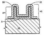
도 5는 유전층, 도전층 및 마스크의 형성 이후 도 3에 도시된 구조와 기판 부분을 도시한 도면.FIG. 5 shows the structure and substrate portions shown in FIG. 3 after formation of the dielectric layer, conductive layer, and mask. FIG.
도 6은 유전층과 도전층의 에칭 이후 그리고 마스크의 제거 이후 도 5에 도시된 구조와 기판 부분을 도시한 도면.FIG. 6 shows the structure and substrate portions shown in FIG. 5 after etching of the dielectric and conductive layers and after removal of the mask. FIG.
도 7은 유전층이 개재된 마스크된 도전층과 기판 부분의 단면도.7 is a cross-sectional view of a masked conductive layer and a substrate portion interposed therebetween with a dielectric layer.
도 8은 도전층과 유전층의 에칭 및 재피착 이후 도 7에 도시된 기판 부분을 도시한 도면.FIG. 8 illustrates a portion of the substrate shown in FIG. 7 after etching and re-deposition of conductive and dielectric layers.
도 9는 마스크의 제거 이후 도 8에 도시된 기판 부분을 도시한 도면.9 shows the substrate portion shown in FIG. 8 after removal of the mask.
도 10은 유전층이 삽입되고 도전 플러그로 마스크화되며 기판 일부 상에 놓여지는 도전층들의 단면도.10 is a cross-sectional view of conductive layers having a dielectric layer inserted therein and masked with a conductive plug and placed over a portion of the substrate.
도 11은 도전층들과 유전층의 에칭과 재피착 이후 도 10의 기판 부분을 도시한 도면.FIG. 11 illustrates the substrate portion of FIG. 10 after etching and re-deposition of conductive layers and dielectric layers. FIG.
도 12는 도전 플러그의 측벽 상에 재피착되는 유전층과 도전층의 단면도.12 is a cross-sectional view of a dielectric layer and a conductive layer deposited on the sidewalls of the conductive plug.
도 13은 본 발명의 구조와 등가인 주사형 전자 마이크로스코프로 촬영한 사진의 복사본.Figure 13 is a copy of a photograph taken with a scanning electron microscope equivalent to the structure of the present invention.
도 14는 본 발명의 구조의 단면도를 나타낸 주사형 전자 마이크로스코프로 촬영한 사진의 복사본.Fig. 14 is a copy of a photograph taken with a scanning electron microscope showing a sectional view of the structure of the present invention.
피착된 재료의 에칭 동안 피착된 재료를 재피착하여 구조를 형성하는 방법이 개시된다. 이 재피착은 에칭이 피착된 재료의 입자들을 가속화한다는 점에서 기계적이며, 기초의 밤바드(bombard) 측벽중 일부가 가속된 입자들이 재피착된 재료를 형성할 수 있는 베이스(base)를 생성하기 위해 제공된다. 따라서, 재피착된 재료는 초기에 피착된 (또는 형성된) 재료와 동일한 화학적 조성을 갖는다.A method is disclosed for re-depositing a deposited material to form a structure during etching of the deposited material. This re-deposition is mechanical in that the etching accelerates the particles of the deposited material, and some of the base bombard sidewalls create a base from which the accelerated particles can form the re-deposited material. Is provided for. Thus, the re-deposited material has the same chemical composition as the material initially deposited (or formed).
도 1에 도시된 일실시예에서, 초기 재료(5)는 기판(10) 상에 놓여지도록 피착된다. 바람직한 실시예에서는, 초기 재료(5)로서 백금(platinum)이 사용되었지만, TiPt, TiNPt, TiAIN-Pt, Ru, Ru02, RuPt, RuO2Pt, W, WPt, WSi, Ti, TiSi, Ta, TaN, TaSi, 도핑(doping) 및 비도핑된 폴리 Si, Al, Pd 및 Ir 같은 다른 재료들이 사용될 수도 있다. 기초(15)는 초기 재료(5) 상에 놓여지도록 형성된다. 본 실시예에서, 기초(15)는 포토레지스트 마스크이며, 그 크기는 사진에칭 기술(photolithic technique)에 의해서만 제한된다. 첨부된 도면에 도시된 기초(15)가 직사각형이라 할지라도, 어떠한 형태로도 형성될 수 있다. 초기 재료(5)는 RF 이온 소오스(20)와 같은 이온 밀(Ion Mill) 에칭기를 사용하여 무선 주파수에서 아르곤 플라즈마 분위기에서 에칭된다. 이온 밀 에칭기 내의 아르곤에 의한 에칭은 본 분야의 숙련된 기술자들에게 공지되어 있다. 또한, 에칭제(etchant)로서 다른 재료를 사용할 수도 있다.In one embodiment shown in FIG. 1,
초기 재료(5)의 일부, 이 경우, 백금을 에칭하는 동안, 도 2에 도시된 기초(15)의 측벽 상에 일부(25)가 재피착된다. 통상적으로, 초기 재료(5)와 가속된 에칭제 이온 궤도 사이의 입사각은 기초(15)의 측벽상에 초기 재료(5)의 재피착의 양을 최대화하기 위하여 선택된다. 통상적으로 90°의 입사각이 바람직하다.During etching of a portion of the
도 3 및 도 4에 있어서, 포토레지스트는 본 발명의 방법에 의해 형성된 백금의 일부(5, 25)를 구성하는 구조(27)를 남겨두고 스트립(strip)된다.In Figures 3 and 4, the photoresist is stripped leaving the
백금 구조(27)는 내장 셀 커패시터를 위한 저장 노드 전극으로서 사용될 수 있다. 이 경우, 커패시터 제조를 완성하기 위하여, 도 5 및 도 6에서와 같이 공정이 진행된다.The
도 5에서, 유전층(30)은 백금 구조(27) 상에 놓여지도록 피착된다. 이러한 피착에 이어서, 도전층(35)을 유전층(30) 상에 놓여지도록 피착, 전형적으로 스퍼터링한다. 그 다음, 유전층(30)과 도전층(35)을 마스크(38)를 이용하여 패턴화한다. 유전층(30)과 도전층(35)은 본 기술 분야의 숙련된 자들에 의해 공지된 수단에 의해 에칭되어 도 6에 도시된 커패시터(40)를 형성한다.In FIG. 5,
오스뮴(Osmium), 이리듐(Iridium), 혹은 루데늄(Ruthenium)이 백금대신 사용된 경우에는, 본 발명의 공정에 의해 형성된 구조들이 산화되어 각각 OsOX, IrO2, 혹은 RuO2를 형성한다.When osmium, iridium, or ruthenium is used instead of platinum, the structures formed by the process of the present invention are oxidized to form OsO X , I r O 2 , or RuO 2 , respectively. .
도 7 내지 도 9에 도시된 다른 실시예에 있어서, 3개의 초기 재료 및 유전층(60)이 삽입된 2개의 도전층들(50, 55)은 기판(65) 상에 놓여지도록 피착된다(도 7을 참조). 이 도전층들(50, 55)이 기초(70), 통상 포토레지스트 마스크에 의해 패턴화된 다음, 도전층들(50, 55)과 유전층(60)이 본래의 위치에서 통상 단일 에칭 단계에 의해 에칭된다.In other embodiments shown in FIGS. 7-9, two
도 8에서, 도전층(55)이 에칭될 때, 이는 기초(70)의 측벽 상에 재피착되어, (기판에 대해) 수직인 도전층(75)을 형성한다. 에칭이 연속해서 행해지며 유전층(60)은 재피착되어 수직 유전층(80)을 형성한다. 에칭 동안 재피착된 도전층(50)이 지속적으로 더욱 에칭하게 되면 수직 도전층(90)이 형성된다. 도전층들(50, 55)으로서 적합한 재료로는 백금, 도전성 산화물 및 폴리실리콘이 있다. 재피착된 층들(75, 90)은 본래의 도전층들(50, 55)과 동일한 재료이다. 따라서, 도전층들(50, 55)이 백금이라면, 재피착된 층들(75, 90)도 또한 백금이다. 유전층의 경우도 이와 동일하다. 유전층(60)은 Ba(1-x)SrxO3, PbZr(1-x)TixO3, LA 등과 같은 다양한 도펀트를 가지는 PZT, Sr(1-x)BixTaO3, Sr(1-x)BixTiO3와 다른 모든 스몰렌스키(smolenski) 화합물, PbMg(1-x)NbxTiO3(PMN), PbTiO3(PMN-PT)를 갖는 화합물, CaBi2Nb2O9, SrBi2Nb2O9, BaBi2Nb2O9, PbBi2NB2O9, BiBi2NbTiO9, BaBi4Ti4O15, CaBi2Ta2O9, SrBi2Ta2O9, BaBi2Ta2O9, PbBi2Ta2O9, Bi4Ti3O12, SrBi4Ti4O15, BaBi4Ti4O15, PbBi4Ti4O15, (Pb, Sr)Bi2Nb2O9, (Pb, Ba)Bi2Nb2O9, (Ba, Ca)Bi2Nb2O9, (Ba, Sr)Bi2Nb2O9, BaBi2Nb2O9, Ba0.75Bi2.25Ti0.25Nb1.75O9, Ba0.5Bi2.5Ti0.5Nb1.5O9, Ba0.25Bi2.75Ti0.75Nb1.25O9, Bi3TiNbO9, SrBi2Nb2O9, Sr0.8Bi2.2Ti0.2Nb1.8O9, Sr0.6Bi2.4Ti0.4Nb1.6O9, Bi3TiNbO9, PbBi2Nb2O9, Pb0.75Bi2.25Ti0.25Nb1.75O9, Pb0.5Bi2.5Ti0.5Nb1.5O9, Pb0.25Bi2.75Ti0.75Nb1.25O9, Bi3TiNbO9, PbBi4Ti4O15, Pb0.75Bi4.25Ti3.75Ga0.25O15, Pb0.5Bi4.5Ti3.5Ga0.5O15, 및 Bi5Ti3GaO15으로 이루어진 그룹으로부터 선택된 유전체 그룹으로부터 선택될 수 있다. 공정 단계들을 최소화하기 위하여, 하나의 에칭제와 단일 에칭 단계를 사용하는 것이 바람직하기는 하지만, 본 발명의 방법을 다수의 에칭제 또는 다수의 에칭 단계들을 사용하여 수행할 수동 있다.In FIG. 8, when the
이전 실시예에서와 같이 기초(70)는 도 9에 도시된 바와 같이 종래의 방법을 사용하여 제거된다. 본 발명의 구조(100)가 남게된다. 이 경우, 구조(100)는 입사각이 90°인 RF 이온 소오스와 같은 이온 밀 에칭기를 사용하여 무선 주파수에서 아르곤 플라즈마 분위기 내에서 수행되는 단일 에칭 공정을 사용하여 형성된 저장 셀 커패시터이다. 에칭제과 입사각을 포함한 이러한 에칭 변수들은 에칭 동안 소정의 측벽 피착이 행해지는 한 사용될 수 있다.As in the previous embodiment, the
또 다른 실시예에서는, 도 10 및 도 11에 도시된 바와 같이, 피착된 유전층(115)이 삽입된 두개의 도전층들(105, 110)이 기판(120)상에 놓여지도록 피착된다. 도전 플러그(125)는 도전층(105) 상에 놓여지도록 종래의 수단에 의해 제조된다. 도전 플러그(125)의 하나의 바람직한 예로서 폴리실리콘 플러그를 선택할 수 있지만, 도전 플러그(125)는 TiPt, TiNPt, TiAlN-Pt, Ru, RuO2, RuPt, RuO2Pt, W, WPt, WSi, Ti, TiSi, Ta, TaN, TaSi, 도핑 및 비도핑된 폴리 Si, Al, Pd 및 Ir로 이루어진 그룹 중에서 선택된 재료일 수 있다. 다른 도전성 재료들도 사용될 수 있다.In another embodiment, as shown in FIGS. 10 and 11, two
도 11은 층들(105, 110, 115)의 에칭 이후의 도전층들(105 및 110)의 재피착 및 유전층(115)의 재피착을 도시한다. 축적 노드 커패시터(130)가 재피착 동안 형성된다. 축적 노드 커패시터(130)는 축적 노드 전극으로서 도전층(110)을 갖고 셀 플레이트 전극으로서 도전층(105)과 도전 플러그(125)를 가진다.FIG. 11 shows re-deposition of
다른 교체가능한 실시예에서, 도전층(105)의 피착은 생략될 수 있다. 이와 같이 형성된 축적 노드 전극에서는, 축적 노드 전극으로서 도전층(110)을 가지며 도 12에 도시된 바와 같이 셀 플레이트 전극으로서 도전 플러그(125)를 가진다.In other replaceable embodiments, deposition of the
도 13은 본 발명의 구조와 등가인 주사형 전자 마이크로스코프에 의해 촬영한 사진의 복사본이고, 도 14는 본 발명의 구조의 단면도를 도시한 주사형 전자 마이크로스코프에 의해 촬영한 사진의 복사본이다.Fig. 13 is a copy of a photograph taken by a scanning electron microscope equivalent to the structure of the present invention, and Fig. 14 is a copy of a photograph taken by a scanning electron microscope showing a sectional view of the structure of the present invention.
Claims (11)
Applications Claiming Priority (2)
| Application Number | Priority Date | Filing Date | Title |
|---|---|---|---|
| US39594195A | 1995-02-28 | 1995-02-28 | |
| US8/395941 | 1995-02-28 |
Publications (2)
| Publication Number | Publication Date |
|---|---|
| KR19980702594A KR19980702594A (en) | 1998-07-15 |
| KR100271111B1 true KR100271111B1 (en) | 2000-12-01 |
Family
ID=23565182
Family Applications (1)
| Application Number | Title | Priority Date | Filing Date |
|---|---|---|---|
| KR1019970706000A Expired - Fee Related KR100271111B1 (en) | 1995-02-28 | 1996-02-21 | Method for forming a structure using redeposition |
Country Status (7)
| Country | Link |
|---|---|
| US (1) | US5792593A (en) |
| EP (2) | EP0812472B1 (en) |
| JP (1) | JP3101685B2 (en) |
| KR (1) | KR100271111B1 (en) |
| AT (1) | ATE220478T1 (en) |
| DE (1) | DE69622261T2 (en) |
| WO (1) | WO1996027208A1 (en) |
Families Citing this family (20)
| Publication number | Priority date | Publication date | Assignee | Title |
|---|---|---|---|---|
| EP0865079A3 (en) * | 1997-03-13 | 1999-10-20 | Applied Materials, Inc. | A method for removing redeposited veils from etched platinum surfaces |
| US6027860A (en) * | 1997-08-13 | 2000-02-22 | Micron Technology, Inc. | Method for forming a structure using redeposition of etchable layer |
| TW430900B (en) * | 1997-09-08 | 2001-04-21 | Siemens Ag | Method for producing structures having a high aspect ratio |
| US6919168B2 (en) | 1998-01-13 | 2005-07-19 | Applied Materials, Inc. | Masking methods and etching sequences for patterning electrodes of high density RAM capacitors |
| US6265318B1 (en) * | 1998-01-13 | 2001-07-24 | Applied Materials, Inc. | Iridium etchant methods for anisotropic profile |
| JP2002510146A (en) | 1998-01-13 | 2002-04-02 | アプライド マテリアルズ インコーポレイテッド | Etching method for anisotropic platinum profile |
| US6323132B1 (en) | 1998-01-13 | 2001-11-27 | Applied Materials, Inc. | Etching methods for anisotropic platinum profile |
| TW434907B (en) * | 1998-12-09 | 2001-05-16 | Matsushita Electronics Corp | Semiconductor memory apparatus and its manufacturing method |
| US6294836B1 (en) * | 1998-12-22 | 2001-09-25 | Cvc Products Inc. | Semiconductor chip interconnect barrier material and fabrication method |
| DE19911150C1 (en) * | 1999-03-12 | 2000-04-20 | Siemens Ag | Microelectronic structure, especially semiconductor memory, production comprising physically etching a conductive layer from a substrate such that removed material is transferred onto a layer structure side wall |
| US6358857B1 (en) | 1999-07-23 | 2002-03-19 | Micron Technology, Inc. | Methods of etching insulative materials, of forming electrical devices, and of forming capacitors |
| US6540928B1 (en) | 1999-09-10 | 2003-04-01 | Unaxis Usa Inc. | Magnetic pole fabrication process and device |
| US6547975B1 (en) * | 1999-10-29 | 2003-04-15 | Unaxis Usa Inc. | Magnetic pole fabrication process and device |
| US6627995B2 (en) | 2000-03-03 | 2003-09-30 | Cvc Products, Inc. | Microelectronic interconnect material with adhesion promotion layer and fabrication method |
| US6444263B1 (en) | 2000-09-15 | 2002-09-03 | Cvc Products, Inc. | Method of chemical-vapor deposition of a material |
| US6533408B1 (en) | 2001-06-21 | 2003-03-18 | Eastman Kodak Company | Ink jet printing method |
| DE10147929C1 (en) * | 2001-09-28 | 2003-04-17 | Infineon Technologies Ag | Method of manufacturing a semiconductor structure and use of the method |
| KR100438781B1 (en) * | 2001-12-05 | 2004-07-05 | 삼성전자주식회사 | Metal - Insulator - Metal capacitor and Method for manufacturing the same |
| KR101934037B1 (en) * | 2012-11-21 | 2018-12-31 | 삼성전자주식회사 | Semiconductor device having supporter and method of forming the same |
| CN113745402B (en) * | 2020-05-29 | 2023-10-17 | 中芯国际集成电路制造(上海)有限公司 | Semiconductor structure, forming method thereof and memory |
Citations (1)
| Publication number | Priority date | Publication date | Assignee | Title |
|---|---|---|---|---|
| JPS63211740A (en) * | 1987-02-27 | 1988-09-02 | Oki Electric Ind Co Ltd | Method for forming wiring pattern of semiconductor element |
Family Cites Families (8)
| Publication number | Priority date | Publication date | Assignee | Title |
|---|---|---|---|---|
| US4432132A (en) * | 1981-12-07 | 1984-02-21 | Bell Telephone Laboratories, Incorporated | Formation of sidewall oxide layers by reactive oxygen ion etching to define submicron features |
| US4400257A (en) * | 1982-12-21 | 1983-08-23 | Rca Corporation | Method of forming metal lines |
| US5185058A (en) * | 1991-01-29 | 1993-02-09 | Micron Technology, Inc. | Process for etching semiconductor devices |
| TW243541B (en) * | 1991-08-31 | 1995-03-21 | Samsung Electronics Co Ltd | |
| JP2953220B2 (en) * | 1992-10-30 | 1999-09-27 | 日本電気株式会社 | Method for manufacturing semiconductor device |
| KR960006822B1 (en) * | 1993-04-15 | 1996-05-23 | 삼성전자주식회사 | Method of micropattern at semiconductor devices |
| US5320981A (en) * | 1993-08-10 | 1994-06-14 | Micron Semiconductor, Inc. | High accuracy via formation for semiconductor devices |
| US5451543A (en) * | 1994-04-25 | 1995-09-19 | Motorola, Inc. | Straight sidewall profile contact opening to underlying interconnect and method for making the same |
-
1996
- 1996-02-21 DE DE69622261T patent/DE69622261T2/en not_active Expired - Lifetime
- 1996-02-21 EP EP96905568A patent/EP0812472B1/en not_active Expired - Lifetime
- 1996-02-21 KR KR1019970706000A patent/KR100271111B1/en not_active Expired - Fee Related
- 1996-02-21 AT AT96905568T patent/ATE220478T1/en not_active IP Right Cessation
- 1996-02-21 JP JP08526340A patent/JP3101685B2/en not_active Expired - Fee Related
- 1996-02-21 EP EP01204492A patent/EP1202331A3/en not_active Withdrawn
- 1996-02-21 WO PCT/US1996/002413 patent/WO1996027208A1/en not_active Ceased
-
1997
- 1997-08-13 US US08/905,785 patent/US5792593A/en not_active Expired - Lifetime
Patent Citations (1)
| Publication number | Priority date | Publication date | Assignee | Title |
|---|---|---|---|---|
| JPS63211740A (en) * | 1987-02-27 | 1988-09-02 | Oki Electric Ind Co Ltd | Method for forming wiring pattern of semiconductor element |
Also Published As
| Publication number | Publication date |
|---|---|
| ATE220478T1 (en) | 2002-07-15 |
| KR19980702594A (en) | 1998-07-15 |
| JP3101685B2 (en) | 2000-10-23 |
| DE69622261T2 (en) | 2003-03-27 |
| EP0812472A1 (en) | 1997-12-17 |
| US5792593A (en) | 1998-08-11 |
| EP1202331A3 (en) | 2002-07-31 |
| JPH10507037A (en) | 1998-07-07 |
| EP0812472B1 (en) | 2002-07-10 |
| EP1202331A2 (en) | 2002-05-02 |
| DE69622261D1 (en) | 2002-08-14 |
| WO1996027208A1 (en) | 1996-09-06 |
Similar Documents
| Publication | Publication Date | Title |
|---|---|---|
| KR100271111B1 (en) | Method for forming a structure using redeposition | |
| US6955992B2 (en) | One mask PT/PCMO/PT stack etching process for RRAM applications | |
| US6097051A (en) | Semiconductor device and method of fabricating | |
| US7169637B2 (en) | One mask Pt/PCMO/Pt stack etching process for RRAM applications | |
| US6432767B2 (en) | Method of fabricating semiconductor device | |
| JP3701129B2 (en) | Etching method of platinum group metal film and method of forming lower electrode of capacitor using the same | |
| US6054391A (en) | Method for etching a platinum layer in a semiconductor device | |
| KR20020093049A (en) | Method of patterning lead zirconium titanate and barium strontium titanate | |
| US6753133B2 (en) | Method and manufacturing a semiconductor device having a ruthenium or a ruthenium oxide | |
| US6586816B2 (en) | Semiconductor structures formed using redeposition of an etchable layer | |
| JPH1022274A (en) | Etching method and method of manufacturing semiconductor device | |
| KR100224730B1 (en) | Method for forming kpotern of semiconductor device and method for manufacturing capacitor using the same | |
| KR100289389B1 (en) | Capacitor fabrication method of semiconductor device | |
| US7015049B2 (en) | Fence-free etching of iridium barrier having a steep taper angle | |
| KR100632526B1 (en) | Method of Making a Structured Material Layer | |
| JP2000196032A (en) | Manufacture of capacitor and the capacitor | |
| JP2003282839A (en) | Method of manufacturing ferroelectric memory device | |
| KR100359785B1 (en) | Semiconductor device and method for fabricating the same | |
| KR100255660B1 (en) | Method for etching ir electrode | |
| KR100624926B1 (en) | Capacitor Manufacturing Method of Semiconductor Device | |
| US6825116B2 (en) | Method for removing structures | |
| KR20030093785A (en) | Method for forming ferroelectric capacitor | |
| KR20010018060A (en) | Method of manufacturing contact hole opening top node of ferroelectric capacitor | |
| KR20020045683A (en) | Method for fabricating capacitor of semiconductor device | |
| KR20020009696A (en) | Method for forming pattern capable of removing polymer generated on sidewall of photoresist pattern and method for forming ferroelectric capacitor using the same |
Legal Events
| Date | Code | Title | Description |
|---|---|---|---|
| A201 | Request for examination | ||
| PA0105 | International application |
St.27 status event code: A-0-1-A10-A15-nap-PA0105 |
|
| PA0201 | Request for examination |
St.27 status event code: A-1-2-D10-D11-exm-PA0201 |
|
| R17-X000 | Change to representative recorded |
St.27 status event code: A-3-3-R10-R17-oth-X000 |
|
| P11-X000 | Amendment of application requested |
St.27 status event code: A-2-2-P10-P11-nap-X000 |
|
| P13-X000 | Application amended |
St.27 status event code: A-2-2-P10-P13-nap-X000 |
|
| PG1501 | Laying open of application |
St.27 status event code: A-1-1-Q10-Q12-nap-PG1501 |
|
| R18-X000 | Changes to party contact information recorded |
St.27 status event code: A-3-3-R10-R18-oth-X000 |
|
| PN2301 | Change of applicant |
St.27 status event code: A-3-3-R10-R11-asn-PN2301 St.27 status event code: A-3-3-R10-R13-asn-PN2301 |
|
| R18-X000 | Changes to party contact information recorded |
St.27 status event code: A-3-3-R10-R18-oth-X000 |
|
| E902 | Notification of reason for refusal | ||
| PE0902 | Notice of grounds for rejection |
St.27 status event code: A-1-2-D10-D21-exm-PE0902 |
|
| T11-X000 | Administrative time limit extension requested |
St.27 status event code: U-3-3-T10-T11-oth-X000 |
|
| P11-X000 | Amendment of application requested |
St.27 status event code: A-2-2-P10-P11-nap-X000 |
|
| P13-X000 | Application amended |
St.27 status event code: A-2-2-P10-P13-nap-X000 |
|
| E701 | Decision to grant or registration of patent right | ||
| PE0701 | Decision of registration |
St.27 status event code: A-1-2-D10-D22-exm-PE0701 |
|
| GRNT | Written decision to grant | ||
| PR0701 | Registration of establishment |
St.27 status event code: A-2-4-F10-F11-exm-PR0701 |
|
| PR1002 | Payment of registration fee |
Fee payment year number: 1 St.27 status event code: A-2-2-U10-U12-oth-PR1002 |
|
| PG1601 | Publication of registration |
St.27 status event code: A-4-4-Q10-Q13-nap-PG1601 |
|
| PR1001 | Payment of annual fee |
Fee payment year number: 4 St.27 status event code: A-4-4-U10-U11-oth-PR1001 |
|
| PR1001 | Payment of annual fee |
Fee payment year number: 5 St.27 status event code: A-4-4-U10-U11-oth-PR1001 |
|
| PR1001 | Payment of annual fee |
Fee payment year number: 6 St.27 status event code: A-4-4-U10-U11-oth-PR1001 |
|
| PR1001 | Payment of annual fee |
Fee payment year number: 7 St.27 status event code: A-4-4-U10-U11-oth-PR1001 |
|
| PR1001 | Payment of annual fee |
Fee payment year number: 8 St.27 status event code: A-4-4-U10-U11-oth-PR1001 |
|
| PR1001 | Payment of annual fee |
Fee payment year number: 9 St.27 status event code: A-4-4-U10-U11-oth-PR1001 |
|
| PR1001 | Payment of annual fee |
Fee payment year number: 10 St.27 status event code: A-4-4-U10-U11-oth-PR1001 |
|
| PR1001 | Payment of annual fee |
Fee payment year number: 11 St.27 status event code: A-4-4-U10-U11-oth-PR1001 |
|
| R18-X000 | Changes to party contact information recorded |
St.27 status event code: A-5-5-R10-R18-oth-X000 |
|
| FPAY | Annual fee payment |
Payment date: 20110630 Year of fee payment: 12 |
|
| PR1001 | Payment of annual fee |
Fee payment year number: 12 St.27 status event code: A-4-4-U10-U11-oth-PR1001 |
|
| FPAY | Annual fee payment |
Payment date: 20120719 Year of fee payment: 13 |
|
| PR1001 | Payment of annual fee |
Fee payment year number: 13 St.27 status event code: A-4-4-U10-U11-oth-PR1001 |
|
| LAPS | Lapse due to unpaid annual fee | ||
| PC1903 | Unpaid annual fee |
Not in force date: 20130811 Payment event data comment text: Termination Category : DEFAULT_OF_REGISTRATION_FEE St.27 status event code: A-4-4-U10-U13-oth-PC1903 |
|
| PC1903 | Unpaid annual fee |
Ip right cessation event data comment text: Termination Category : DEFAULT_OF_REGISTRATION_FEE Not in force date: 20130811 St.27 status event code: N-4-6-H10-H13-oth-PC1903 |
|
| P22-X000 | Classification modified |
St.27 status event code: A-4-4-P10-P22-nap-X000 |
|
| P22-X000 | Classification modified |
St.27 status event code: A-4-4-P10-P22-nap-X000 |
|
| P22-X000 | Classification modified |
St.27 status event code: A-4-4-P10-P22-nap-X000 |