JPWO2018230039A1 - Antenna device - Google Patents
Antenna device Download PDFInfo
- Publication number
- JPWO2018230039A1 JPWO2018230039A1 JP2019525071A JP2019525071A JPWO2018230039A1 JP WO2018230039 A1 JPWO2018230039 A1 JP WO2018230039A1 JP 2019525071 A JP2019525071 A JP 2019525071A JP 2019525071 A JP2019525071 A JP 2019525071A JP WO2018230039 A1 JPWO2018230039 A1 JP WO2018230039A1
- Authority
- JP
- Japan
- Prior art keywords
- antenna
- antenna element
- slot
- antenna device
- radiation pattern
- Prior art date
- Legal status (The legal status is an assumption and is not a legal conclusion. Google has not performed a legal analysis and makes no representation as to the accuracy of the status listed.)
- Granted
Links
Images


Classifications
-
- H—ELECTRICITY
- H01—ELECTRIC ELEMENTS
- H01Q—ANTENNAS, i.e. RADIO AERIALS
- H01Q13/00—Waveguide horns or mouths; Slot antennas; Leaky-waveguide antennas; Equivalent structures causing radiation along the transmission path of a guided wave
- H01Q13/10—Resonant slot antennas
-
- H—ELECTRICITY
- H01—ELECTRIC ELEMENTS
- H01Q—ANTENNAS, i.e. RADIO AERIALS
- H01Q21/00—Antenna arrays or systems
- H01Q21/06—Arrays of individually energised antenna units similarly polarised and spaced apart
- H01Q21/08—Arrays of individually energised antenna units similarly polarised and spaced apart the units being spaced along or adjacent to a rectilinear path
-
- H—ELECTRICITY
- H01—ELECTRIC ELEMENTS
- H01Q—ANTENNAS, i.e. RADIO AERIALS
- H01Q1/00—Details of, or arrangements associated with, antennas
- H01Q1/12—Supports; Mounting means
- H01Q1/22—Supports; Mounting means by structural association with other equipment or articles
- H01Q1/24—Supports; Mounting means by structural association with other equipment or articles with receiving set
- H01Q1/241—Supports; Mounting means by structural association with other equipment or articles with receiving set used in mobile communications, e.g. GSM
- H01Q1/242—Supports; Mounting means by structural association with other equipment or articles with receiving set used in mobile communications, e.g. GSM specially adapted for hand-held use
- H01Q1/243—Supports; Mounting means by structural association with other equipment or articles with receiving set used in mobile communications, e.g. GSM specially adapted for hand-held use with built-in antennas
-
- H—ELECTRICITY
- H01—ELECTRIC ELEMENTS
- H01Q—ANTENNAS, i.e. RADIO AERIALS
- H01Q1/00—Details of, or arrangements associated with, antennas
- H01Q1/48—Earthing means; Earth screens; Counterpoises
-
- H—ELECTRICITY
- H01—ELECTRIC ELEMENTS
- H01Q—ANTENNAS, i.e. RADIO AERIALS
- H01Q1/00—Details of, or arrangements associated with, antennas
- H01Q1/52—Means for reducing coupling between antennas; Means for reducing coupling between an antenna and another structure
- H01Q1/521—Means for reducing coupling between antennas; Means for reducing coupling between an antenna and another structure reducing the coupling between adjacent antennas
- H01Q1/523—Means for reducing coupling between antennas; Means for reducing coupling between an antenna and another structure reducing the coupling between adjacent antennas between antennas of an array
-
- H—ELECTRICITY
- H01—ELECTRIC ELEMENTS
- H01Q—ANTENNAS, i.e. RADIO AERIALS
- H01Q21/00—Antenna arrays or systems
- H01Q21/06—Arrays of individually energised antenna units similarly polarised and spaced apart
- H01Q21/061—Two dimensional planar arrays
- H01Q21/064—Two dimensional planar arrays using horn or slot aerials
-
- H—ELECTRICITY
- H01—ELECTRIC ELEMENTS
- H01Q—ANTENNAS, i.e. RADIO AERIALS
- H01Q21/00—Antenna arrays or systems
- H01Q21/24—Combinations of antenna units polarised in different directions for transmitting or receiving circularly and elliptically polarised waves or waves linearly polarised in any direction
-
- H—ELECTRICITY
- H01—ELECTRIC ELEMENTS
- H01Q—ANTENNAS, i.e. RADIO AERIALS
- H01Q21/00—Antenna arrays or systems
- H01Q21/28—Combinations of substantially independent non-interacting antenna units or systems
-
- H—ELECTRICITY
- H01—ELECTRIC ELEMENTS
- H01Q—ANTENNAS, i.e. RADIO AERIALS
- H01Q9/00—Electrically-short antennas having dimensions not more than twice the operating wavelength and consisting of conductive active radiating elements
- H01Q9/04—Resonant antennas
- H01Q9/0407—Substantially flat resonant element parallel to ground plane, e.g. patch antenna
- H01Q9/0428—Substantially flat resonant element parallel to ground plane, e.g. patch antenna radiating a circular polarised wave
- H01Q9/0435—Substantially flat resonant element parallel to ground plane, e.g. patch antenna radiating a circular polarised wave using two feed points
Landscapes
- Engineering & Computer Science (AREA)
- Computer Networks & Wireless Communication (AREA)
- Variable-Direction Aerials And Aerial Arrays (AREA)
- Waveguide Aerials (AREA)
Abstract
【課題】複数のアンテナ素子をアレイ化する場合においても、より好適な放射パターンを得ることを可能とする。【解決手段】誘電体基板と、第1の方向に沿って配設され、それぞれが、偏波方向が互いに異なる第1の無線信号及び第2の無線信号を送信または受信する複数のアンテナ素子と、互いに隣り合う第1の及び第2のアンテナ素子間に対応する領域に第2の方向に延伸するように長尺状のスロットが設けられたグランド板と、を備え、無線信号の波長をλ0、誘電体基板の比誘電率をεr1、グランド板に対して誘電体基板とは逆側に位置する誘電体の比誘電率をεr2とした場合に、スロットの第2の方向の長さLが以下に示す条件式を満たす、アンテナ装置。【数1】【選択図】図9PROBLEM TO BE SOLVED: To obtain a more preferable radiation pattern even when arraying a plurality of antenna elements. A dielectric substrate and a plurality of antenna elements arranged along a first direction and transmitting or receiving a first radio signal and a second radio signal each having a different polarization direction. , A ground plate provided with elongated slots extending in the second direction in regions corresponding to the first and second antenna elements adjacent to each other, and the wavelength of the radio signal is λ0. When the relative permittivity of the dielectric substrate is εr1 and the relative permittivity of the dielectric on the side opposite to the dielectric substrate with respect to the ground plate is εr2, the length L of the slot in the second direction is An antenna device that satisfies the following conditional expression. [Formula 1] [Selection diagram] Fig. 9
Description
本開示は、アンテナ装置に関する。 The present disclosure relates to an antenna device.
LTE/LTE−A(Advanced)と呼ばれる通信規格に基づく移動体通信システムにおいては、主に、700MHz〜3.5GHz前後の極超短波と呼ばれる周波数の無線信号が通信に利用されている。 2. Description of the Related Art In a mobile communication system based on a communication standard called LTE / LTE-A (Advanced), a radio signal of a frequency called a very high frequency of about 700 MHz to about 3.5 GHz is mainly used for communication.
また、上記通信規格のような極超短波を利用した通信では、所謂MIMO(Multiple−Input and Multiple−Output)と呼ばれる技術を採用することで、フェージング環境下においても、直接波に加えて反射波を信号の送受信に利用して通信性能をより向上させることが可能となる。MIMOでは、複数のアンテナを使用することとなるため、スマートフォン等のような移動体通信の端末装置に対して、複数のアンテナをより好適な態様で配設する手法についても各種検討されている。 Also, in communication using ultra high frequency waves as in the above communication standard, by employing a so-called MIMO (Multiple-Input and Multiple-Output) technique, even in a fading environment, reflected waves can be generated in addition to direct waves. It is possible to further improve the communication performance by utilizing the signal transmission / reception. In MIMO, since a plurality of antennas are used, various methods for arranging the plurality of antennas in a more suitable manner for a mobile communication terminal device such as a smartphone have been studied.
また、近年では、LTE/LTE−Aに続く第5世代(5G)移動体通信システムについて各種検討がされている。例えば、同移動体通信システムでは、28GHzや39GHzといったミリ波と呼ばれる周波数の無線信号(以下、単に「ミリ波」とも称する)を利用した通信の利用が検討されている。 In recent years, various studies have been made on a fifth generation (5G) mobile communication system following LTE / LTE-A. For example, in the mobile communication system, use of communication using a radio signal of a frequency called a millimeter wave such as 28 GHz or 39 GHz (hereinafter, also simply referred to as “millimeter wave”) is being studied.
ミリ波は、極超短波に比べて伝送される情報の量を増加させることが可能となる一方で、直進性が高く伝搬ロスや反射損失が増大する傾向にある。そのため、ミリ波を利用した無線通信においては、主に直接波が通信特性に寄与し、反射波の影響をほとんど受けないことがわかっている。このような特性から、5Gの移動体通信システムにおいては、偏波方向が互いに異なる複数の偏波(例えば、水平偏波及び垂直偏波)を利用してMIMOを実現する、偏波MIMOと呼ばれる技術の導入も検討されている。 Millimeter waves can increase the amount of information transmitted as compared with ultrahigh frequency waves, but tend to have high straightness and increase propagation loss and reflection loss. Therefore, in wireless communication using millimeter waves, it has been found that direct waves mainly contribute to communication characteristics and are hardly affected by reflected waves. From such characteristics, in a 5G mobile communication system, MIMO is realized using a plurality of polarizations having different polarization directions (for example, horizontal polarization and vertical polarization), which is called polarization MIMO. The introduction of technology is also being considered.
ところで、一般的にはミリ波は空間減衰が比較的大きく、ミリ波を通信に利用する場合には、利得の高いアンテナが求められる傾向にある。このような要求を実現するために、所謂ビームフォーミングと呼ばれる技術が利用される場合がある。具体的には、ビームフォーミングによりアンテナのビーム幅を制御し、ビームの指向性を向上させることで、アンテナの利得をより向上させることが可能となる。このような制御を実現可能なアンテナ方式の一例として、パッチアレイアンテナが挙げられる。例えば、特許文献1には、パッチアレイアンテナの一例が開示されている。
By the way, in general, millimeter waves have relatively large spatial attenuation, and when millimeter waves are used for communication, there is a tendency that an antenna having a high gain is required. In order to realize such a demand, a technique called beam forming may be used. Specifically, by controlling the beam width of the antenna by beam forming and improving the directivity of the beam, it is possible to further improve the gain of the antenna. An example of an antenna system that can realize such control is a patch array antenna. For example,
一方で、複数のアンテナ素子(例えば、パッチアンテナ)のアレイ化に伴い、少なくとも一部のアンテナ素子の放射パターンに歪が生じる場合がある。このように、放射パターンに歪が生じることにより、所定の空間中の少なくとも一部の領域において、所望の利得を得ることが困難となる場合がある。 On the other hand, with the arraying of a plurality of antenna elements (for example, patch antennas), the radiation pattern of at least some of the antenna elements may be distorted. As described above, when the radiation pattern is distorted, it may be difficult to obtain a desired gain in at least a part of the predetermined space.
そこで、本開示では、複数のアンテナ素子をアレイ化する場合においても、より好適な放射パターンを得ることが可能な技術の一例について提案する。 Therefore, the present disclosure proposes an example of a technique capable of obtaining a more suitable radiation pattern even when a plurality of antenna elements are arrayed.
本開示によれば、略平面状の誘電体基板と、前記誘電体基板の一方の面上に、当該誘電体基板の平面に対して水平な第1の方向に沿って配設され、それぞれが、偏波方向が互いに異なる第1の無線信号及び第2の無線信号を送信または受信する複数のアンテナ素子と、前記誘電体基板の他方の面の略全体に設けられ、互いに隣り合う第1のアンテナ素子及び第2のアンテナ素子の間に対応する領域に、前記第1の方向に直交する第2の方向に延伸するように長尺状のスロットが設けられたグランド板と、を備え、前記複数のアンテナ素子それぞれの共振周波数の中心周波数の波長をλ0、前記誘電体基板の比誘電率をεr1、前記グランド板に対して前記誘電体基板とは逆側に位置する誘電体の比誘電率をεr2とした場合に、前記スロットの前記第2の方向の長さLが以下に示す条件式を満たす、アンテナ装置が提供される。According to the present disclosure, a substantially planar dielectric substrate and, on one surface of the dielectric substrate, disposed along a first direction that is horizontal to a plane of the dielectric substrate. A plurality of antenna elements for transmitting or receiving the first wireless signal and the second wireless signal having different polarization directions, and a first antenna element provided on substantially the entire other surface of the dielectric substrate and adjacent to each other; A ground plate provided with an elongated slot so as to extend in a second direction orthogonal to the first direction, in a region corresponding to between the antenna element and the second antenna element; The wavelength of the center frequency of the resonance frequency of each of the plurality of antenna elements is λ 0 , the relative permittivity of the dielectric substrate is ε r1 , the ratio of the dielectric located on the opposite side of the dielectric substrate to the ground plate. when the dielectric constant was epsilon r2, the slot The second direction of the length L satisfies the condition expressed by the following, the antenna device is provided.

以上説明したように本開示によれば、複数のアンテナ素子をアレイ化する場合においても、より好適な放射パターンを得ることが可能な技術が提供される。 As described above, according to the present disclosure, a technique capable of obtaining a more suitable radiation pattern even when a plurality of antenna elements are arrayed is provided.
なお、上記の効果は必ずしも限定的なものではなく、上記の効果とともに、または上記の効果に代えて、本明細書に示されたいずれかの効果、または本明細書から把握され得る他の効果が奏されてもよい。 Note that the above effects are not necessarily limited, and any of the effects shown in the present specification or other effects that can be grasped from the present specification are used together with or in place of the above effects. May be played.
以下に添付図面を参照しながら、本開示の好適な実施の形態について詳細に説明する。なお、本明細書及び図面において、実質的に同一の機能構成を有する構成要素については、同一の符号を付することにより重複説明を省略する。 Hereinafter, preferred embodiments of the present disclosure will be described in detail with reference to the accompanying drawings. In the specification and the drawings, components having substantially the same functional configuration are denoted by the same reference numerals, and redundant description is omitted.
なお、説明は以下の順序で行うものとする。
1.概略構成
1.1.システム構成の一例
1.2.端末装置の機能構成
1.3.端末装置の構成例
2.ミリ波を利用した通信に関する検討
3.技術的特徴
3.1.構成
3.2.変形例
3.3.実施例
3.4.応用例
4.むすびThe description will be made in the following order.
1. Schematic configuration 1.1. Example of system configuration 1.2. Functional configuration of terminal device 1.3. 1. Configuration example of terminal device Study on communication using millimeter wave Technical features 3.1. Configuration 3.2. Modification 3.3. Example 3.4. Application example 4. Conclusion
<<1.概略構成>>
<1.1.システム構成の一例>
まず、図1を参照して、本開示の一実施形態に係るシステム1の概略的な構成の一例について説明する。図1は、本開示の一実施形態に係るシステム1の概略的な構成の一例について説明するための説明図である。図1に示すように、システム1は、無線通信装置100と、端末装置200とを含む。ここでは、端末装置200は、ユーザとも呼ばれる。当該ユーザは、UEとも呼ばれ得る。無線通信装置100Cは、UE−Relayとも呼ばれる。ここでのUEは、LTE又はLTE−Aにおいて定義されているUEであってもよく、UE−Relayは、3GPPで議論されているProse UE to Network Relayであってもよく、より一般的に通信機器を意味してもよい。<< 1. Schematic configuration >>
<1.1. Example of system configuration>
First, an example of a schematic configuration of a
(1)無線通信装置100
無線通信装置100は、配下の装置に無線通信サービスを提供する装置である。例えば、無線通信装置100Aは、セルラーシステム(又は移動体通信システム)の基地局である。基地局100Aは、基地局100Aのセル10Aの内部に位置する装置(例えば、端末装置200A)との無線通信を行う。例えば、基地局100Aは、端末装置200Aへのダウンリンク信号を送信し、端末装置200Aからのアップリンク信号を受信する。(1) Wireless communication device 100
The wireless communication device 100 is a device that provides a wireless communication service to subordinate devices. For example, the
基地局100Aは、他の基地局と例えばX2インタフェースにより論理的に接続されており、制御情報等の送受信が可能である。また、基地局100Aは、所謂コアネットワーク(図示を省略する)と例えばS1インタフェースにより論理的に接続されており、制御情報等の送受信が可能である。なお、これらの装置間の通信は、物理的には多様な装置により中継され得る。
The
ここで、図1に示した無線通信装置100Aは、マクロセル基地局であり、セル10Aはマクロセルである。一方で、無線通信装置100B及び100Cは、スモールセル10B及び10Cをそれぞれ運用するマスタデバイスである。一例として、マスタデバイス100Bは、固定的に設置されるスモールセル基地局である。スモールセル基地局100Bは、マクロセル基地局100Aとの間で無線バックホールリンクを、スモールセル10B内の1つ以上の端末装置(例えば、端末装置200B)との間でアクセスリンクをそれぞれ確立する。なお、無線通信装置100Bは、3GPPで定義されるリレーノードであってもよい。マスタデバイス100Cは、ダイナミックAP(アクセスポイント)である。ダイナミックAP100Cは、スモールセル10Cを動的に運用する移動デバイスである。ダイナミックAP100Cは、マクロセル基地局100Aとの間で無線バックホールリンクを、スモールセル10C内の1つ以上の端末装置(例えば、端末装置200C)との間でアクセスリンクをそれぞれ確立する。ダイナミックAP100Cは、例えば、基地局又は無線アクセスポイントとして動作可能なハードウェア又はソフトウェアが搭載された端末装置であってよい。この場合のスモールセル10Cは、動的に形成される局所的なネットワーク(Localized Network/Virtual Cell)である。
Here,
セル10Aは、例えば、LTE、LTE−A(LTE-Advanced)、LTE−ADVANCED PRO、GSM(登録商標)、UMTS、W−CDMA、CDMA200、WiMAX、WiMAX2又はIEEE802.16などの任意の無線通信方式に従って運用されてよい。
The
なお、スモールセルは、マクロセルと重複して又は重複せずに配置される、マクロセルよりも小さい様々な種類のセル(例えば、フェムトセル、ナノセル、ピコセル及びマイクロセルなど)を含み得る概念である。ある例では、スモールセルは、専用の基地局によって運用される。別の例では、スモールセルは、マスタデバイスとなる端末がスモールセル基地局として一時的に動作することにより運用される。いわゆるリレーノードもまた、スモールセル基地局の一形態であると見なすことができる。リレーノードの親局として機能する無線通信装置は、ドナー基地局とも称される。ドナー基地局は、LTEにおけるDeNBを意味してもよく、より一般的にリレーノードの親局を意味してもよい。 Note that the small cell is a concept that can include various types of cells (for example, femtocells, nanocells, picocells, microcells, and the like) smaller than the macrocell and arranged so as to overlap or not overlap with the macrocell. In one example, a small cell is operated by a dedicated base station. In another example, a small cell is operated by a terminal serving as a master device temporarily operating as a small cell base station. So-called relay nodes can also be considered as a form of small cell base station. A wireless communication device functioning as a master station of a relay node is also called a donor base station. The donor base station may mean a DeNB in LTE, and may more generally mean a parent station of a relay node.
(2)端末装置200
端末装置200は、セルラーシステム(又は移動体通信システム)において通信可能である。端末装置200は、セルラーシステムの無線通信装置(例えば、基地局100A、マスタデバイス100B又は100C)との無線通信を行う。例えば、端末装置200Aは、基地局100Aからのダウンリンク信号を受信し、基地局100Aへのアップリンク信号を送信する。(2)
The
また、端末装置200としては、所謂UEのみに限らず、例えば、MTC端末、eMTC(Enhanced MTC)端末、及びNB−IoT端末等のような所謂ローコスト端末(Low cost UE)が適用されてもよい。
Further, as the
(3)補足
以上、システム1の概略的な構成を示したが、本技術は図1に示した例に限定されない。例えば、システム1の構成として、マスタデバイスを含まない構成、SCE(Small Cell Enhancement)、HetNet(Heterogeneous Network)、MTCネットワーク等が採用され得る。またシステム1の構成の、他の一例として、マスタデバイスがスモールセルに接続し、スモールセルの配下でセルを構築してもよい。(3) Supplement Although the schematic configuration of the
以上、図1を参照して、本開示の一実施形態に係るシステム1の概略的な構成の一例について説明した。
The example of the schematic configuration of the
<1.2.端末装置の機能構成>
次に、図2を参照して、本開示の実施形態に係る端末装置200の機能構成の一例を説明する。図2は、本開示の実施形態に係る端末装置200の構成の一例を示すブロック図である。図2に示すように、端末装置200は、アンテナ部2001と、無線通信部2003と、記憶部2007と、通信制御部2005とを含む。<1.2. Functional configuration of terminal device>
Next, an example of a functional configuration of the
(1)アンテナ部2001
アンテナ部2001は、無線通信部2003により出力される信号を電波として空間に放射する。また、アンテナ部2001は、空間の電波を信号に変換し、当該信号を無線通信部2003へ出力する。(1)
The
(2)無線通信部2003
無線通信部2003は、信号を送受信する。例えば、無線通信部2003は、基地局からのダウンリンク信号を受信し、基地局へのアップリンク信号を送信する。(2)
(3)記憶部2007
記憶部2007は、端末装置200の動作のためのプログラム及び様々なデータを一時的に又は恒久的に記憶する。(3)
The
(4)、通信制御部2005
通信制御部2005は、無線通信部2003の動作を制御することで、他の装置(例えば、基地局100)との間の通信を制御する。具体的な一例として、通信制御部2005は、送信対象となるデータを所定の変調方式に基づき変調することで送信信号を生成し、無線通信部2003に当該送信信号を基地局100に向けて送信させてもよい。また、他の一例として、通信制御部2005は、基地局100からの信号の受信結果(即ち、受信信号)を無線通信部2003から取得し、当該受信信号に対して所定の復調処理を施すことで当該基地局100から送信されたデータを復調してもよい。(4),
The
以上、図2を参照して、本開示の実施形態に係る端末装置200の機能構成の一例を説明した。
The example of the functional configuration of the
<1.3.通信装置の構成例>
続いて、本実施形態に係る通信装置の構成の一例として、上述した端末装置200のような通信装置に対して、パッチアンテナ(平面アンテナ)をアレイ化した所謂パッチアレイアンテナを適用した場合の一例について説明する。<1.3. Configuration example of communication device>
Subsequently, as an example of the configuration of the communication device according to the present embodiment, an example in which a so-called patch array antenna in which patch antennas (planar antennas) are arrayed is applied to a communication device such as the
まず、図3を参照して、パッチアンテナの概要について説明する。図3は、パッチアンテナの概要について説明するための説明図である。一般的に知られているアンテナの一例として、所謂ダイポールアンテナは、エレメントが棒状のため電流の流れる向きが1方向となり、送信または受信可能な偏波が1偏波のみとなる。これに対して、パッチアンテナは、給電点を複数設けることで、複数方向に電流を流すことが可能である。例えば、図3に示すパッチアンテナ2111は、平面状のエレメント2112に対して複数の給電点2113及び2114が設けられており、偏波方向が互いに異なる(互いに直交する)偏波RH及びRVそれぞれを送信または受信可能に構成されている。First, an outline of the patch antenna will be described with reference to FIG. FIG. 3 is an explanatory diagram for describing an overview of the patch antenna. As an example of a generally known antenna, a so-called dipole antenna has a rod-shaped element, so that current flows in one direction, and only one polarized wave can be transmitted or received. On the other hand, the patch antenna can supply current in a plurality of directions by providing a plurality of feeding points. For example, a
次いで、図4を参照して、本実施形態に係る通信装置の構成の一例について説明する。図4は、本実施形態に係る通信装置の構成の一例について説明するための説明図である。なお、以降の説明では、本実施形態に係る通信装置を、「通信装置211」と称する場合がある。
Next, an example of the configuration of the communication device according to the present embodiment will be described with reference to FIG. FIG. 4 is an explanatory diagram for describing an example of the configuration of the communication device according to the present embodiment. In the following description, the communication device according to the present embodiment may be referred to as a “
本実施形態に係る通信装置211は、略長方形の形状を成す表面及び裏面を有する板状の筐体209を備えている。なお、本説明では、ディスプレイ等の表示部が設けられた側の面を表面と称する。即ち、図4において、参照符号201は、筐体209の外面のうち裏面を示している。また、参照符号203及び205は、筐体209の外面のうち裏面201の周囲に位置する一端面に相当し、より具体的には、当該裏面201の長手方向に延伸する端面を示している。また、参照符号202及び204は、筐体209の外面のうち裏面201の周囲に位置する一端面に相当し、より具体的には、当該裏面201の短手方向に延伸する端面を示している。なお、図3において図示を省略しているが、裏面201の反対側に位置する表面を、便宜上「表面206」とも称する。
The
また、図4において、参照符号2110a〜2110fのそれぞれは、基地局との間で無線信号(例えば、ミリ波)を送受信するためのアンテナ装置を示している。なお、以降の説明では、アンテナ装置2110a〜2110fを特に区別しない場合には、単に「アンテナ装置2110」と称する場合がある。
In FIG. 4,
図4に示すように、本実施形態に係る通信装置211は、裏面201及び端面202〜205のそれぞれについて、当該面の少なくとも一部の近傍に位置するように、筐体209の内部にアンテナ装置2110が保持(設置)されている。
As shown in FIG. 4, the
また、アンテナ装置2110は、複数のアンテナ素子2111を含んでいる。より具体的には、アンテナ装置2110は、複数のアンテナ素子2111をアレイ化することで、アレイアンテナとして構成されている。例えば、アンテナ素子2111aは、裏面201のうち端面204側の端部近傍に位置するように保持され、複数のアンテナ素子2111が、当該端部が延伸する方向(即ち、端面204の長手方向)に沿って配列されるように設けられている。また、アンテナ素子2111dは、端面205の一部の近傍に位置するように保持され、複数のアンテナ素子2111が、当該端面205の長手方向に沿って配列されるように設けられている。
The
また、ある面の近傍に位置するように保持されるアンテナ装置2110において、各アンテナ素子2111は、平面状のエレメント(例えば、図3に示すエレメント2112)の法線方向が、当該面の法線方向と略一致するように保持される。より具体的な一例として、アンテナ装置2110aに着目した場合には、当該アンテナ装置2110aに設けられたアンテナ素子2111は、平面状のエレメントの法線方向が、裏面201の法線方向と略一致するように保持される。これは、他のアンテナ装置2110b〜2110fについても同様である。
Further, in the
以上のような構成により、各アンテナ装置2110は、複数のアンテナ素子2111それぞれにより送信または受信される無線信号の位相や電力を制御することで、当該無線信号の指向性を制御する(即ち、ビームフォーミングを行う)ことが可能となる。
With the above-described configuration, each
以上、図4を参照して、本実施形態に係る通信装置の構成の一例について説明した。なお、上述したアンテナ装置2110の構成はあくまで一例であり、アンテナ装置2110の構成を必ずしも限定するものではない。例えば、複数のアンテナ素子2111のそれぞれが、アンテナ装置2110が近傍に保持される面の法線方向と略一致する方向に伝搬する無線信号を送信または受信することが可能であれば、複数のアンテナ素子2111それぞれが配置される位置は限定されない。即ち、複数のアンテナ素子2111は、必ずしも、図4に示すように、一方向に沿ってのみ配列されていなくてもよい。例えば、複数のアンテナ素子2111が、行列状に配列されていてもよい。
The example of the configuration of the communication device according to the present embodiment has been described above with reference to FIG. Note that the configuration of the
<<2.ミリ波を利用した通信に関する検討>>
LTE/LTE−A等の規格に基づく通信システムでは、700MHz〜3.5GHz前後の極超短波と呼ばれる周波数の無線信号が通信に利用されている。これに対して、LTE/LTE−Aに続く第5世代(5G)移動体通信システムでは、28GHzや39GHzといったミリ波と呼ばれる周波数の無線信号(以下、単に「ミリ波」とも称する)を利用した通信の利用が検討されている。そこで、ミリ波を利用した通信の概要について説明したうえで、本開示の一実施形態に係る通信装置の技術的課題について整理する。<< 2. Study on communication using millimeter waves >>
2. Description of the Related Art In a communication system based on a standard such as LTE / LTE-A, a radio signal having a frequency called an ultrahigh frequency of about 700 MHz to about 3.5 GHz is used for communication. On the other hand, in the fifth generation (5G) mobile communication system following LTE / LTE-A, a radio signal of a frequency called a millimeter wave such as 28 GHz or 39 GHz (hereinafter, also simply referred to as “millimeter wave”) is used. The use of communication is being considered. Therefore, after an outline of communication using millimeter waves is described, technical issues of the communication device according to an embodiment of the present disclosure will be summarized.
LTE/LTE−Aのような極超短波を利用した通信では、所謂MIMO(Multiple−Input and Multiple−Output)と呼ばれる技術を採用することで、フェージング環境下においても、直接波に加えて反射波を信号の送受信に利用して通信性能をより向上させることが可能である。 In communication using ultra high frequency waves such as LTE / LTE-A, a technique called MIMO (Multiple-Input and Multiple-Output) is employed, so that a reflected wave can be added to a direct wave even in a fading environment. It is possible to further improve the communication performance by utilizing the signal transmission / reception.
これに対して、ミリ波は、極超短波に比べて伝送される情報の量を増加させることが可能となる一方で、直進性が高く伝搬ロスや反射損失が増大する傾向にある。そのため、無線信号が送受信されるアンテナ間を直接結ぶ経路上に障害物が存在しない環境(所謂LOS:Line of Site)においては、反射波の影響をほとんど受けずに、主に直接波が通信特性に寄与することとなる。このような特性から、ミリ波を利用した通信においては、例えば、スマートフォン等のような通信端末が、基地局から直接送信される無線信号(即ち、ミリ波)を受信する(即ち、直接波を受信する)ことで、通信性能をより向上させることが可能となる。 On the other hand, the millimeter wave can increase the amount of information transmitted as compared with the ultrashort wave, but tends to have high straightness and increase propagation loss and reflection loss. Therefore, in an environment where there is no obstacle on a path directly connecting antennas for transmitting and receiving wireless signals (so-called LOS: Line of Site), the direct wave is mainly affected by the communication characteristics without being largely affected by the reflected wave. Will be contributed to. From such characteristics, in communication using a millimeter wave, for example, a communication terminal such as a smartphone receives a radio signal (that is, a millimeter wave) transmitted directly from a base station (that is, a direct wave is transmitted). Receiving) makes it possible to further improve the communication performance.
一方で、一般的には、ミリ波は空間減衰が比較的大きく、ミリ波を通信に利用する場合には、利得の高いアンテナが求められる傾向にある。このようなより高い利得を実現するために、例えば、ビームフォーミングと呼ばれる技術が利用される場合がある。具体的には、ビームフォーミングによりアンテナのビーム幅を制御し、ビームの指向性を向上させることで、アンテナの利得をより向上させることが可能となる。しかしながら、ビームの指向性を向上させることで、ビーム幅がより狭くなり、上記アンテナによりカバーできる空間が制限される場合もある。そのため、このような場合には、例えば、ビームの方向を時分割で制御することにより、より広い空間を上記アンテナによりカバーする場合もある。上記のような制御を実現可能なアンテナ方式の一例として、パッチアレイアンテナが挙げられる。 On the other hand, in general, millimeter waves have relatively large spatial attenuation, and when millimeter waves are used for communication, there is a tendency for an antenna having a high gain to be required. In order to realize such higher gain, for example, a technique called beamforming may be used. Specifically, by controlling the beam width of the antenna by beam forming and improving the directivity of the beam, it is possible to further improve the gain of the antenna. However, by improving the directivity of the beam, the beam width becomes narrower, and the space that can be covered by the antenna may be limited. Therefore, in such a case, for example, a wider space may be covered by the antenna by controlling the direction of the beam by time division. An example of an antenna system capable of realizing the above control is a patch array antenna.
一方で、複数のアンテナ素子(例えば、パッチアンテナ)のアレイ化に伴い、少なくとも一部のアンテナ素子の放射パターンに歪が生じる場合がある。ここで、図5〜図8を参照して、複数のアンテナ素子のアレイ化に伴い生じる放射パターンの歪の一例について説明する。図5〜図8は、複数のアンテナ素子のアレイ化に伴い生じる放射パターンの歪の一例について説明するための説明図である。なお、本説明では、アンテナ素子として図3を参照して説明したようなパッチアンテナ(平面アンテナ)を適用した場合を例に、放射パターンのシミュレーション結果の一例について説明する。また、図5〜図8に示す例においては、便宜上、アンテナ素子を構成する平面状のエレメントの法線方向をz方向とし、当該エレメントの平面に水平な互いに直交する方向をx方向及びy方向とする。 On the other hand, with the arraying of a plurality of antenna elements (for example, patch antennas), the radiation pattern of at least some of the antenna elements may be distorted. Here, with reference to FIGS. 5 to 8, an example of a distortion of a radiation pattern caused by arraying a plurality of antenna elements will be described. FIG. 5 to FIG. 8 are explanatory diagrams for explaining an example of distortion of a radiation pattern caused by arraying a plurality of antenna elements. In the present description, an example of a simulation result of a radiation pattern will be described using a case where a patch antenna (planar antenna) as described with reference to FIG. 3 is applied as an antenna element. In addition, in the examples shown in FIGS. 5 to 8, for convenience, the normal direction of the planar element constituting the antenna element is defined as the z direction, and the directions orthogonal to each other and horizontal to the plane of the element are defined as the x and y directions. And
まず、図5及び図6を参照して、アンテナ素子が1つの場合における、当該アンテナ素子の放射パターンのシミュレーション結果の一例について説明する。 First, with reference to FIGS. 5 and 6, an example of a simulation result of a radiation pattern of the antenna element when there is one antenna element will be described.
例えば、図5は、本実施形態に係るアンテナ装置に適用可能な、パッチアンテナとして構成されたアンテナ素子単体の概略的な構成の一例を示している。図5に示すように、パッチアンテナとして構成されたアンテナ素子2111は、平面状のエレメント2112に対して給電点2113及び2114が設けられている。具体的には、エレメント2112は、誘電体により形成された略平面状の誘電体基板2115の一方の面に設けられている。また、誘電体基板2115の他方の面、即ち、エレメント2112が設けられた面とは逆側の面には、当該面の略全体をカバーするように略平面状のグランド板2116が設けられている。また、給電点2113及び2114のそれぞれは、エレメント2112の法線方向に沿って誘電体基板2115を貫通し、当該エレメント2112とグランド板2116とを電気的に接続するように設けられている。
For example, FIG. 5 shows an example of a schematic configuration of a single antenna element configured as a patch antenna applicable to the antenna device according to the present embodiment. As shown in FIG. 5, an
また、図6は、図5を参照して説明したアンテナ素子2111の放射特性に応じた放射パターンのシミュレーション結果の一例を示している。図6に示すように、アンテナ素子2111を単体で使用した場合には、歪の少ない(理想的には歪の無い)放射パターンが形成される。
FIG. 6 shows an example of a simulation result of a radiation pattern according to the radiation characteristics of the
次いで、図7及び図8を参照して、図5に示すアンテナ素子2111をアレイ化した場合における、当該アンテナ素子2111の放射パターンのシミュレーション結果の一例について説明する。
Next, an example of a simulation result of a radiation pattern of the
例えば、図7は、図5に示すアンテナ素子2111が複数設けられることで、パッチアレイアンテナとして構成されたアンテナ装置2910の概略的な構成の一例を示している。図7に示すように、アンテナ装置2910は、誘電体基板2115の一方の面上に所定の方向(y方向)に沿って3つのアンテナ素子2111が配設されて構成されている。なお、本説明では、便宜上、y方向に配設された3つのアンテナ素子2111のうち、中央に配設されたアンテナ素子2111を「アンテナ素子2111a」と称し、他の2つのアンテナ素子2111を「アンテナ素子2111b」及び「アンテナ素子2111c」と称する。また、誘電体基板2115の他方の面には、当該面の略全体をカバーするように略平面状のグランド板2116が設けられている。アンテナ素子2111a〜2111cそれぞれの給電点2113及び2114は、それぞれが対応するエレメント2112の法線方向に沿って誘電体基板2115を貫通し、当該エレメント2112と上記グランド板2116とを電気的に接続するように設けられている。
For example, FIG. 7 illustrates an example of a schematic configuration of an
また、図8は、図7を参照して説明したアンテナ装置2910におけるアンテナ素子2111aの放射特性に応じた放射パターンのシミュレーション結果の一例を示している。図8と図6とを比較するとわかるように、図8に示す例では、アンテナ素子2111a〜2111cをy方向に沿ってアレイ化することにより、少なくとも一部のアンテナ素子2111(例えば、アンテナ素子2111a)の放射パターンに歪が生じている(即ち、±y方向にビームスプリットが生じている)。このように放射パターンに歪が生じることで、例えば、アンテナ素子2111aを介した無線信号の送信または受信に際し、所定の空間中の少なくとも一部の領域において、所望の利得を得ることが困難となる場合がある。
FIG. 8 shows an example of a simulation result of a radiation pattern according to the radiation characteristics of the
以上のような状況を鑑み、本開示では、複数のアンテナ素子をアレイ化する場合においても、より好適な放射パターンを得ることが可能な技術の一例について提案する。 In view of the above situation, the present disclosure proposes an example of a technique capable of obtaining a more suitable radiation pattern even when a plurality of antenna elements are arrayed.
<<3.技術的特徴>>
続いて、本開示の一実施形態に係る通信装置の技術的特徴について説明する。<< 3. Technical features >>
Subsequently, the technical features of the communication device according to an embodiment of the present disclosure will be described.
<3.1.構成>
まず、本実施形態に係るアンテナ装置の基本的な構成について、複数のアンテナ素子をアレイ化する場合に、少なくとも一部のアンテナ素子について放射パターンの歪を抑制するための構成に着目して説明する。<3.1. Configuration>
First, a basic configuration of the antenna device according to the present embodiment will be described by focusing on a configuration for suppressing a distortion of a radiation pattern of at least a part of the antenna elements when a plurality of antenna elements are arrayed. .
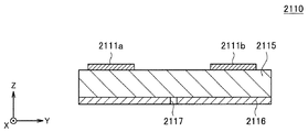
まず、図9を参照して、本実施形態に係るアンテナ装置の基本構成について概要を説明する。図9は、本実施形態に係るアンテナ装置の概略的な構成について説明するための説明図であり、パッチアンテナがアレイ化されたパッチアレイアンテナの構成の一例を示している。なお、図9に示す例では、図7に示す例と同様に、便宜上、アンテナ素子を構成する平面状のエレメントの法線方向をz方向とし、当該エレメントの平面に水平な互いに直交する方向をx方向及びy方向とする。また、図9に示す例では、図7を参照して説明した例と同様に、誘電体基板2115の一方の面上に、y方向に沿って、アンテナ素子2111c、2111a、及び2111bがこの順で配設されているものとする。
First, an outline of a basic configuration of the antenna device according to the present embodiment will be described with reference to FIG. FIG. 9 is an explanatory diagram for describing a schematic configuration of the antenna device according to the present embodiment, and illustrates an example of a configuration of a patch array antenna in which patch antennas are arrayed. In the example illustrated in FIG. 9, similarly to the example illustrated in FIG. 7, for convenience, the normal direction of the planar element forming the antenna element is set to the z direction, and the directions that are perpendicular to the plane of the element are orthogonal to each other. The directions are the x direction and the y direction. In the example shown in FIG. 9, similarly to the example described with reference to FIG. 7, on one surface of the
図9に示すように、本実施形態に係るアンテナ装置2110は、グランド板2116に対してスロット2117a及び2117bが設けられている点で、図7を参照して説明したアンテナ装置2910と異なる。
As shown in FIG. 9, the
ここで、図10及び図11を参照して、本実施形態に係るアンテナ装置2110の特徴的な構成について、特に、図9に示すアンテナ素子2111a及び2111bが配設された部分の構成に着目して説明する。図10は、本実施形態に係るアンテナ装置2110の概略的な平面図であり、アンテナ装置2110を上方(z方向)から見た場合における、アンテナ素子2111a及び2111bが配設された部分の概略的な構成の一例を示している。また、図11は、図10に示したアンテナ装置2110の概略的なA−A’断面図である。なお、図10及び図11では、アンテナ素子2111a及び2111bそれぞれの給電点2113及び2114については図示を省略している。
Here, with reference to FIG. 10 and FIG. 11, regarding the characteristic configuration of the
図10及び図11に示すように、本実施形態に係るアンテナ装置2110においては、グランド板2116に対して、互いに隣り合う2つのアンテナ素子2111(例えば、アンテナ素子2111a及び2111b)の間に対応する領域にスロット2117が設けられている。スロット2117は、上記2つのアンテナ素子2111が配列された方向(y方向)と直交する方向(x方向)に延伸するように長尺状に形成されている。なお、以降においては、複数のアンテナ素子2111が配列された方向を「配列方向」とも称する。また、スロット2117を設ける位置や、当該スロット2117のサイズ等については、別途詳細を後述する。また、図10及び図11に示すスロット2117は、例えば、図9に示す例においけるスロット2117aに相当する。
As shown in FIG. 10 and FIG. 11, in the
なお、複数のアンテナ素子2111の配列方向が、「第1の方向」の一例に相当し、当該配列方向と直交する方向(即ち、スロット2117が延伸する方向)が「第2の方向」の一例に相当する。また、アンテナ素子2111が送信または受信する偏波方向が互いに異なる複数の偏波のうち、偏波方向が第1の方向と略一致する信号が「第1の無線信号」の一例に相当し、偏波方向が第2の方向と略一致する信号が「第2の無線信号」の一例に相当する。
Note that the arrangement direction of the plurality of
また、図10及び図11に示す例では、アンテナ素子2111a及び2111bが配設された部分に着目して示しているが、アンテナ素子2111a及び2111cが配設された部分についても同様である。即ち、図10及び図11に示す例において、アンテナ素子2111bをアンテナ素子2111cに置き換えた構成が、アンテナ装置2110におけるアンテナ素子2111a及び2111cが配設された部分の構成と略等しい構成を示している。また、この場合におけるスロット2117は、例えば、図9に示す例におけるスロット2117bに相当する。
In addition, in the examples shown in FIGS. 10 and 11, attention is paid to the portion where the
次いで、図9を参照して説明したアンテナ装置2110におけるアンテナ素子2111aの放射パターンについて説明する。例えば、図12は、本実施形態に係るアンテナ装置の放射パターンについて説明するための説明図であり、図9を参照して説明したアンテナ装置2110におけるアンテナ素子2111aの放射特性に応じた放射パターンのシミュレーション結果の一例を示している。図12を図8と比較するとわかるように、本実施形態に係るアンテナ装置2110においては、図7に示すアンテナ装置2910において生じていた放射パターンの歪が改善されていることがわかる。即ち、本実施形態に係るアンテナ装置2110に依れば、アンテナ素子2111のアレイ化に伴い生じる放射パターンの歪(即ち、図8に示すような±y方向のビームスプリット)を改善し、アンテナ素子2111単体の場合における放射パターン(図6に示す放射パターン)により近づけることが可能となる。
Next, a radiation pattern of the
続いて、図13を参照して、スロット2117を設ける位置や、当該スロット2117のサイズの詳細について説明する。図13は、本実施形態に係るアンテナ装置の構成の一例について説明するための説明図である。図13は、図10と同様に、アンテナ装置2110を上方(z方向)から見た場合における、アンテナ素子2111a及び2111bが配設された部分の概略的な構成の一例を示している。なお、本説明では、アンテナ素子2111aが、主に放射パターンの歪改善の対象となるアンテナ素子(以降では、単に「改善対象のアンテナ素子」とも称する)に相当するものとして説明する。なお、改善対象のアンテナ素子2111aが「第1のアンテナ素子」の一例に相当し、当該アンテナ素子2111aの隣に位置するアンテナ素子2111bが「第2のアンテナ素子」の一例に相当する。
Subsequently, referring to FIG. 13, details of the position where the
図13において、参照符号aは、アンテナ素子2111の各端部の幅のうち、複数のアンテナ素子2111の配列方向(図13におけるy方向)の幅を示している。また、参照符号dは、互いに隣り合う2つのアンテナ素子2111それぞれの中心間の距離(図13におけるy方向の距離)を示している。なお、以降の説明では、当該距離dを、「素子間隔d」とも称する。また、参照符号Lは、スロット2117のスロット長を示している。より具体的には、スロット長Lは、スロット2117の長尺方向の幅、即ち、複数のアンテナ素子2111の配列方向と直交する方向(図13におけるx方向)の幅に相当する。また、参照符号pは、互いに隣り合う2つのアンテナ素子2111のうち第1のアンテナ素子2111(即ち、アンテナ素子2111a)の中心と、スロット2117の配列方向の中心と、の間の距離(即ち、配列方向の距離)を示している。即ち、距離pは、第1のアンテナ素子2111を基点として、スロット2117が設けられた位置(図13におけるy方向の位置)を示している。なお、以降の説明では、スロット2117が設けられた位置を「スロット位置」とも称する。
In FIG. 13, reference numeral “a” indicates a width in the arrangement direction of the plurality of antenna elements 2111 (y direction in FIG. 13) among the widths of the respective ends of the
また、本説明において、誘電体基板2115を構成する誘電体の比誘電率をεr1とする。また、グランド板2116に対して、誘電体基板2115とは逆側に位置する誘電体の比誘電率をεr2とする。なお、グランド板2116において誘電体基板2115が設けられた面とは逆側の面側に位置する誘電体が空気の場合(例えば、他の基板等が設けられていない場合)には、比誘電率εr2=1.0となる。また、アンテナ素子2111に送信または受信される無線信号の自由空間における波長をλ0とし、スロットの共振波長をλgとする。Further, in the present description, the relative permittivity of the dielectric constituting the
(スロット長)
まず、本実施形態に係るアンテナ装置2110における、スロット2117のスロット長Lの条件について説明する。本実施形態に係るアンテナ装置2110においては、アンテナ素子2111(特に、第1のアンテナ素子2111)とスロット2117とが結合することにより、グランド板2116を流れる電流(地板電流)が減少し、結果として、アンテナ素子2111の放射パターンの歪が抑制(低減)される。(Slot length)
First, the condition of the slot length L of the
ここで、アンテナ素子2111とスロット2117とが結合するためには、当該スロット2117のスロット長Lが、共振波長λgの1/2以上である必要がある。また、当該共振波長λgは、アンテナ素子2111により送信または受信される無線信号の波長λ0と、スロット2117を囲む空間の比誘電率の平均とにより算出される。Here, since the
即ち、本実施形態に係るアンテナ装置2110においては、スロット2117は、スロット長Lが以下に(式1)及び(式2)で示す条件を満たすように形成される。
That is, in the
(素子間隔)
次いで、本実施形態に係るアンテナ装置2110における、互いに隣り合う2つのアンテナ素子2111の素子間隔dの条件について説明する。素子間隔dは、放射パターンの歪をより低減するという観点に基づくと、互いに隣り合う2つのアンテナ素子2111が可能な限り離間するように設定される方が望ましい。(Element spacing)
Next, the condition of the element interval d between two
一方で、d≧λ0とすると、アレーアンテナとして動作させた場合に、グレーティングローブと呼ばれる不要輻射が発生し、所定の方向について利得が低下する場合がある。これに対して、λ0/2<d<λ0の範囲において、グレーティングローブが発生する素子間隔dは、所要ビーム走査角度に依存する。例えば、図14は、アンテナ素子の間隔と、グレーティングローブが可視領域に出現するビーム走査角との関係の一例を示したグラフである。図14において、横軸は素子間隔をd/λ(λは無線信号の波長)で示しており、縦軸はビーム走査角を示している。On the other hand, if d ≧ λ 0 , unnecessary radiation called a grating lobe occurs when the antenna is operated as an array antenna, and the gain may decrease in a predetermined direction. In contrast, in the lambda 0/2 <range of d <lambda 0, element spacing d of the grating lobes occur depends on the required beam scan angle. For example, FIG. 14 is a graph showing an example of the relationship between the spacing between antenna elements and the beam scanning angle at which the grating lobe appears in the visible region. In FIG. 14, the horizontal axis represents the element spacing by d / λ (λ is the wavelength of the radio signal), and the vertical axis represents the beam scanning angle.
以上のような条件を鑑みると、本実施形態に係るアンテナ装置2110においては、素子間隔dが以下に(式3)で示す条件を満たすように、各アンテナ素子2111が配設されるとより望ましい。
In view of the above-described conditions, in the
(スロット位置)
続いて、本実施形態に係るアンテナ装置2110における、第1のアンテナ素子2111(即ち、改善対象のアンテナ素子2111)を基点としたスロット2117の位置、即ち、当該アンテナ素子2111の中心と、当該スロット2117の配列方向の中心と、の間の距離pの条件に付いて説明する。(Slot position)
Subsequently, in the
スロット2117がアンテナ素子2111のより近傍に位置するほど、当該アンテナ素子2111の性能がより低下する傾向にある。一方で、当該アンテナ素子2111の端部からある程度離間した位置にスロット2117が設けられることで、当該アンテナ素子2111の性能低下の影響がより小さくなる。即ち、距離pの最小値については、互いに隣り合う2つのアンテナ素子2111のうち、第1のアンテナ素子2111のエッジに係る直前の位置にスロット2117が位置する場合の距離とすることが望ましい。また、距離pの最大値については、第1のアンテナ素子2111の隣に位置する第2のアンテナ素子2111のエッジに係る直前の位置にスロット2117が位置する場合の距離とすることが望ましい。
As the
以上のような条件に基づき、アンテナ素子2111の一辺の幅aが以下に(式4)として示す条件を満たすため、距離pは、(式3)として前述した条件を鑑みると、以下に(式5)として示す条件を満たすように設定されることが望ましい。
Based on the above conditions, the width a of one side of the
即ち、本実施形態に係るアンテナ装置2110においては、上述した(式3)〜(式5)で示した条件式に基づき、距離pが以下に(式6)で示す条件を満たすように、スロット2117が設けられるとより望ましい。
That is, in the
以上、図9〜図14を参照して、本実施形態に係るアンテナ装置の基本的な構成について、複数のアンテナ素子をアレイ化する場合に、少なくとも一部のアンテナ素子について放射パターンの歪を抑制するための構成に着目して説明した。 As described above, with reference to FIG. 9 to FIG. 14, in the basic configuration of the antenna device according to the present embodiment, when a plurality of antenna elements are arrayed, distortion of a radiation pattern is suppressed for at least some of the antenna elements The description has been made by focusing on the configuration for performing the above.
なお、上述した本実施形態に係るアンテナ装置の構成はあくまで一例であり、上述した条件を満たせば、当該アンテナ装置の各部の構成は必ずしも上述した例のみには限定されない。具体的な一例として、アンテナ装置に設けられたアンテナ素子の数は、2以上であれば特に限定されない。 The configuration of the antenna device according to the embodiment described above is merely an example, and the configuration of each unit of the antenna device is not necessarily limited to the above-described example as long as the above-described conditions are satisfied. As a specific example, the number of antenna elements provided in the antenna device is not particularly limited as long as it is two or more.
<3.2.変形例>
続いて、本実施形態に係るアンテナ装置の変形例について説明する。<3.2. Modification>
Subsequently, a modified example of the antenna device according to the present embodiment will be described.
(変形例1:アンテナ素子の向きの一例について)
まず、変形例1として、第1のアンテナ素子2111(即ち、改善対象のアンテナ素子)の隣に位置する第2のアンテナ素子2111を設置する向きの一例について説明する。例えば、図15は、変形例1に係るアンテナ装置の構成の一例について説明するための説明図である。なお、図15に示す例では、アンテナ装置に設けられたアンテナ素子を構成する平面状のエレメントの法線方向をz方向とし、当該エレメントの平面に水平な互いに直交する方向をx方向及びy方向とする。即ち、図15は、変形例1に係るアンテナ装置の概略的な平面図であり、アンテナ装置を上方(z方向)から見た場合における当該アンテナ装置の概略的な構成の一例を示している。なお、以降の説明では、変形例1に係るアンテナ装置を、上述した実施形態、他の変形例、及び他の実施例に係るアンテナ装置と区別するために、「アンテナ装置2210」と称する場合がある。(Variation 1: An example of the orientation of the antenna element)
First, as Modification Example 1, an example of a direction in which the
図15に示すように、変形例1に係るアンテナ装置2210は、y方向に沿ってアンテナ素子2111c、2111a、及び2111bがこの順序で配設されている。また、グランド板2116に対してスロット2117a及び2117bが設けられている。具体的には、グランド板2116に対して、アンテナ素子2111a及び2111bの間に対応する領域にスロット2117aが設けられており、アンテナ素子2111a及び2111cの間に対応する領域にスロット2117bが設けられている。即ち、アンテナ装置2210は、上記構成については、図9を参照して前述したアンテナ装置2110と同様の構成を有している。
As shown in FIG. 15, the
一方で、変形例1に係るアンテナ装置2210は、第1のアンテナ素子2111の隣に位置する第2のアンテナ素子2111の向きが、所定の条件に応じて決定される点で、図9を参照して前述したアンテナ装置2110と異なる。
On the other hand, the
具体的には、図15に示す例では、アンテナ素子2111aが「第1のアンテナ素子」に相当し、アンテナ素子2111b及び2111cが当該第1のアンテナ素子の隣に位置する「第2のアンテナ素子」に相当するものとする。この場合に、変形例1に係るアンテナ素子2111b及び2111cについては、偏波方向が図15のy方向と略一致する無線信号に対応する給電点2113が、当該アンテナ素子2111(エレメント2112)のy方向(即ち、配列方向)の端部のうち、アンテナ素子2111aとは逆側の端部の方向に偏心して設けられている。具体的には、アンテナ素子2111bの給電点2113は、アンテナ素子2111aとは逆側の端部(即ち、+y方向側の端部)の方向に偏心して設けられている。また、アンテナ素子2111cの給電点2113については、アンテナ素子2111aとは逆側の端部(即ち、−y方向側の端部)の方向に偏心して設けられている。このように、変形例1に係るアンテナ装置では、第2のアンテナ素子における、複数のアンテナ素子の配列方向と偏波方向が略一致する無線信号に対応する給電点は、当該アンテナ素子における当該配列方向の端部のうち、第1のアンテナ素子とは逆側の端部の方向に偏心して設けられる。なお、給電点2113が「第1の給電点」の一例に相当し、給電点2114が「第2の給電点」の一例に相当する。
Specifically, in the example shown in FIG. 15, the
以上のような構成とすることで、アンテナ素子2111aに対して、アンテナ素子2111b及び2111cそれぞれの給電点2113を、物理的により離隔した位置に設けられることとなる。これにより、アンテナ素子2111b及び2111cそれぞれの給電点2113に対して給電を行った際に、当該アンテナ素子2111b及び2111cのそれぞれと、アンテナ素子2111aとの間の結合が発生する可能性をより低減することが可能となる。換言すると、変形例1に係るアンテナ装置に依れば、第2のアンテナ素子に対する給電に伴う、第1のアンテナ素子への影響をより低減することが可能となる。
With the above structure, the feeding points 2113 of the
以上、変形例1として、図15を参照して、第1のアンテナ素子2111の隣に位置する第2のアンテナ素子2111を設置する向きの一例について説明した。
As above, the example of the direction in which the
<3.3.実施例>
続いて、本実施系形態に係るアンテナ装置の実施例について説明する。<3.3. Example>
Subsequently, an example of the antenna device according to the present embodiment will be described.
(実施例1:4素子アレイ構成)
まず、実施例1として、4つのアンテナ素子をアレイ化することで本実施形態に係るアンテナ装置を構成した場合の一例について説明する。例えば、図16は、実施例1に係るアンテナ装置の構成の一例について説明するための説明図である。なお、図16に示す例では、アンテナ装置に設けられたアンテナ素子を構成する平面状のエレメントの法線方向をz方向とし、当該エレメントの平面に水平な互いに直交する方向をx方向及びy方向とする。即ち、図16は、実施例1に係るアンテナ装置の概略的な平面図であり、アンテナ装置を上方(z方向)から見た場合における当該アンテナ装置の概略的な構成の一例を示している。なお、以降の説明では、実施例1に係るアンテナ装置を、上述した実施形態、他の変形例、及び他の実施例に係るアンテナ装置と区別するために、「アンテナ装置2410」と称する場合がある。(Example 1: Four-element array configuration)
First, as Example 1, an example in which the antenna device according to the present embodiment is configured by arraying four antenna elements will be described. For example, FIG. 16 is an explanatory diagram for describing an example of the configuration of the antenna device according to the first embodiment. In the example shown in FIG. 16, the normal direction of the planar element constituting the antenna element provided in the antenna device is defined as the z direction, and directions orthogonal to each other and horizontal to the plane of the element are defined as the x direction and the y direction. And That is, FIG. 16 is a schematic plan view of the antenna device according to the first embodiment, and illustrates an example of a schematic configuration of the antenna device when the antenna device is viewed from above (z direction). In the following description, the antenna device according to the first embodiment may be referred to as “
図16に示すように、実施例1に係るアンテナ装置2410は、y方向に沿ってアンテナ素子2111d、2111c、2111a、及び2111bがこの順序で配設されている。なお、アンテナ素子2111a〜2111dのうち、アンテナ素子2111aが第1のアンテナ素子(即ち、改善対象のアンテナ素子)に相当し、当該アンテナ素子2111aの隣に位置するアンテナ素子2111b及び2111cが第2のアンテナ素子に相当する。また、以降の説明においては、複数のアンテナ素子2111のうち、第1のアンテナ素子及び第2のアンテナ素子のいずれにも該当しないアンテナ素子2111(例えば、図16に示すアンテナ素子2111d)については、「第3のアンテナ素子」とも称する。
As illustrated in FIG. 16, the
また、グランド板2116に対してスロット2117a及び2117bが設けられている。具体的には、グランド板2116に対して、アンテナ素子2111a(第1のアンテナ素子)とアンテナ素子2111b(第2のアンテナ素子)との間に対応する領域にスロット2117aが設けられている。また、当該グランド板2116に対して、アンテナ素子2111a(第1のアンテナ素子)とアンテナ素子2111c(第2のアンテナ素子)との間に対応する領域にスロット2117bが設けられている。なお、グランド板2116に対して、アンテナ素子2111c(第2のアンテナ素子)とアンテナ素子2111d(第3のアンテナ素子)との間に対応する領域にスロット2117cが設けられていてもよい。また、他の一例として、グランド板2116に対して、当該スロット2117cが設けられていなくてもよい。
Further,
また、変形例1として前述したように、アンテナ素子2111b及び2111c(即ち、第2のアンテナ素子)については、給電点2113が、当該アンテナ素子2111(エレメント2112)のy方向(即ち、配列方向)の端部のうち、アンテナ素子2111a(即ち、第1のアンテナ素子)とは逆側の端部の方向に偏心して設けられていてもよい。例えば、図16に示す例において、アンテナ素子2111bの給電点2113は、アンテナ素子2111aとは逆側の端部(即ち、+y方向側の端部)の方向に偏心して設けられている。また、アンテナ素子2111cの給電点2113については、アンテナ素子2111aとは逆側の端部(即ち、−y方向側の端部)の方向に偏心して設けられている。
As described above as the first modification, for the
以上のような構成とすることで、実施例1に係るアンテナ装置2410に依れば、アンテナ素子2111a〜2111dのうち、少なくともアンテナ素子2111a(即ち、第1のアンテナ素子)の放射パターンの歪をより好適な態様で抑制(低減)することが可能となる。
With the above configuration, according to the
以上、実施例1として、図16を参照して、4つのアンテナ素子をアレイ化することで本実施形態に係るアンテナ装置を構成した場合の一例について説明した。 As above, an example in which the antenna device according to the present embodiment is configured by arraying four antenna elements has been described as Example 1 with reference to FIG.
(実施例2:L字型アンテナ装置)
続いて、実施例2として、2つのアンテナ装置をL字型に連結することで1つのアンテナ装置として構成した場合の一例について説明する。例えば、図17は、実施例2に係るアンテナ装置の構成の一例について説明するための説明図である。なお、以降の説明では、実施例2に係るアンテナ装置を、上述した実施形態、他の変形例、及び他の実施例に係るアンテナ装置と区別するために、「アンテナ装置2510」と称する場合がある。(Example 2: L-shaped antenna device)
Next, an example in which two antenna devices are connected in an L-shape to form one antenna device will be described as a second embodiment. For example, FIG. 17 is an explanatory diagram for describing an example of the configuration of the antenna device according to the second embodiment. In the following description, the antenna device according to the second embodiment may be referred to as “
まず、図17を参照して、実施例2に係るアンテナ装置2510の概略的な構成の一例について説明する。図17は、実施例2に係るアンテナ装置2510の概略的な斜視図である。図17に示すように、アンテナ装置2510は、アンテナ部2410a及び2410bと、連結部2511とを含む。アンテナ部2410a及び2410bのそれぞれは、図16を参照して前述したアンテナ装置2410に相当する。そのため、アンテナ部2410a及び2410bそれぞれの構成について詳細な説明は省略する。なお、アンテナ部2410a及び2410bのうち、一方が「第1のアンテナ部」の一例に相当し、他方が「第2のアンテナ部」の一例に相当する。
First, an example of a schematic configuration of the
また、本説明においては、図17に示すように、アンテナ部2410a及び2410bそれぞれにおいて複数のアンテナ素子2111(即ち、アンテナ素子2111a〜2111d)の配列方向をz方向とする。また、アンテナ部2410aにおいて、各アンテナ素子2111を構成する平面上のエレメントの平面に水平であり、配列方向(z方向)に直交する方向をy方向とする。即ち、アンテナ部2410aにおいては、各スロット2117(即ち、スロット21117a〜2117c)は、y方向に延伸するように設けられている。また、アンテナ部2410bにおいて、各アンテナ素子2111を構成する平面上のエレメントの平面に水平であり、配列方向(z方向)に直交する方向をx方向とする。即ち、アンテナ部2410bにおいては、各スロット2117は、x方向に延伸するように設けられている。
In the present description, as shown in FIG. 17, the arrangement direction of the plurality of antenna elements 2111 (that is,
図17に示すように、アンテナ部2410aとアンテナ部2410bとは、それぞれの端部のうち、複数のアンテナ素子2111の配列方向に延伸する端部の一方が互いに近傍に位置するように配置される。このとき、アンテナ部2410aのアンテナ素子2111と、アンテナ部2410bのアンテナ素子2111とは、平面状のエレメントの法線方向が互い交差する(例えば、直交する)か、または、当該法線方向が互いにねじれの位置にあるように配置されることとなる。また、アンテナ部2410aとアンテナ部2410bとの間で、互いに近傍に位置する端部間を架設するように連結部2511が設けられており、当該連結部2511により当該アンテナ部2410aと当該アンテナ部2410bとが連結されている。即ち、連結部2511により、アンテナ部2410aとアンテナ部2410bとが略L字型を形成するように、当該アンテナ部2410aと当該アンテナ部2410bとが保持される。
As illustrated in FIG. 17, the
以上のような構成を有するアンテナ装置2510については、例えば、図4に示す裏面201と端面204とのように、筐体209の外面のうち互いに連接する複数の面(外面)に沿って保持されるとよい。このような構成により、互いに連接する当該複数の面それぞれについて、当該面に略垂直な方向から到来し、互いに偏波方向の異なる複数の偏波それぞれをより好適な態様で送信または受信することが可能となる。
The
以上、実施例2として、図17を参照して、2つのアンテナ装置をL字型に連結することで1つのアンテナ装置として構成した場合の一例について説明した。なお、実施例2として説明したアンテナ装置の構成はあくまで一例であり、必ずしも本実施形態に係るアンテナ装置の構成を限定するものではない。具体的な一例として、アンテナ部2410a及び2410bそれぞれに設けられるアンテナ素子2111の数については、2以上であれが特に限定されない。また、アンテナ部2410aとアンテナ部2410bとで、それぞれに設けられたアンテナ素子2111の数が異なっていてもよい。また、図13を参照して前述した、スロット長Lと、素子間隔dと、アンテナ素子2111とスロット2117との間の距離p(即ち、スロット位置)と、のそれぞれの条件を満たせば、各部の寸法については限定されない。
As above, an example in which two antenna devices are connected in an L-shape to form one antenna device has been described as the second embodiment with reference to FIG. 17. Note that the configuration of the antenna device described as the second embodiment is only an example, and does not necessarily limit the configuration of the antenna device according to the present embodiment. As a specific example, the number of
(実施例3:シミュレーション結果について)
続いて、実施例3として、スロット長、素子間隔、及びスロット位置の条件に応じた放射パターンのシミュレーション結果の一例について具体的な例を挙げて説明する。(Example 3: Simulation results)
Next, as a third embodiment, an example of a simulation result of a radiation pattern according to conditions of a slot length, an element interval, and a slot position will be described with a specific example.
まず、比較例1として、図18及び図19を参照して、シミュレーションの対象となるアンテナ素子2111単体の構成について説明する。図18及び図19は、比較例1に係るアンテナ素子の構成の一例について説明するための説明図である。具体的には、図18は、比較例1に係るアンテナ素子の概略的な斜視図である。また、図19は、比較例2に係るアンテナ素子を平面状のエレメントの法線方向から見た場合における、当該アンテナ素子の概略的な構成の一例を示している。
First, as Comparative Example 1, a configuration of a
図18に示すように、比較例1に係るアンテナ素子2111は、平面方向の幅それぞれが5mm、厚みが0.4mmとなるように形成されている。また、図19に示すように、本説明では、便宜上、給電点2114を含み、当該給電点2114に対応する信号の偏波方向(図19の縦方向)と、アンテナ素子2112の法線方向(図19の奥行き方向)と、に延伸する平面を「phi0面」と称する。また、給電点2113を含み、当該給電点2113に対応する信号の偏波方向(図19の横方向)と、アンテナ素子2112の法線方向(図19の奥行き方向)と、に延伸する平面を「phi90面」と称する。
As shown in FIG. 18, the
また、給電点2113及び2114への給電に伴い送信される無線信号の周波数を28GHzとする。また、給電点2113及び2114に対応する2偏波は、直線直交2偏波とする。また、誘電体基板2115を形成する誘電体の比誘電率は3.3とする。
Further, the frequency of a wireless signal transmitted along with power supply to the
続いて、図20及び図21を参照して、上記比較例1に係るアンテナ素子2111の放射パターンのシミュレーション結果の一例について説明する。図20及び図21は、比較例1に係るアンテナ素子2111の放射パターンのシミュレーション結果の一例を示した図である。具体的には、図20は、給電点2113への給電に伴い生じる放射パターンをphi90面で切断した場合の放射パターンの一例を示している。図20において、横軸は図18に示すシータ方向の角度(deg)を示しており、縦軸は無線信号の利得(dB)を示している。また、図21は、給電点2114への給電に伴い生じる放射パターンをphi90面で切断した場合の放射パターンの一例を示している。図21における縦軸及び横軸については、図20と同様である。
Subsequently, an example of a simulation result of a radiation pattern of the
図20及び図21に示すように、比較例1に係るアンテナ素子2111については、放射パターンに歪が生じていないことがわかる。
As shown in FIGS. 20 and 21, it can be seen that no distortion occurs in the radiation pattern of the
続いて、比較例2として、比較例1に係るアンテナ素子2111を3つアレイ化したアンテナ装置における放射パターンのシミュレーション結果の一例について説明する。例えば、図22は、比較例2に係るアンテナ装置の概略的な構成の一例について説明するための説明図であり、当該アンテナ装置を平面状のエレメントの法線方向から見た場合における、当該アンテナ素子の概略的な構成の一例を示している。
Subsequently, as Comparative Example 2, an example of a simulation result of a radiation pattern in an antenna device in which three
図22に示す例では、3つのアンテナ素子2111を、給電点2113に対応する信号の偏波方向(図22の横方向)を配列方向としてアレイ化することでアンテナ装置を構成している。即ち、比較例2に係るアンテナ装置の配列方向とphi90面とは平行となり、当該配列方向とphi0面と垂直となる。
In the example shown in FIG. 22, the antenna device is configured by arraying three
なお、本説明では、図7を参照して説明した例と同様に、中央に配設されたアンテナ素子2111を「アンテナ素子2111a」と称し、他の2つのアンテナ素子2111を「アンテナ素子2111b」及び「アンテナ素子2111c」と称する。即ち、アンテナ素子2111aが第1のアンテナ素子に相当し、アンテナ素子2111b及び2111cが第2のアンテナ素子に相当するものとする。
In the present description, similarly to the example described with reference to FIG. 7, the
また、前述したように、複数のアンテナ素子のアレイ化に伴い生じる歪は、主に、当該複数のアンテナ素子の配列方向について生じる傾向にある。そのため、以降の説明では、配列方向に平行なphi90面にのみ着目して、第1のアンテナ素子に相当するアンテナ素子2111aの放射パターンのシミュレーション結果の一例について説明する。
In addition, as described above, the distortion generated due to the arraying of a plurality of antenna elements tends to occur mainly in the arrangement direction of the plurality of antenna elements. Therefore, in the following description, an example of a simulation result of the radiation pattern of the
例えば、図23及び図24は、比較例2に係るアンテナ装置の放射パターンのシミュレーション結果の一例を示している。具体的には、具体的には、図23は、給電点2114への給電に伴い生じるアンテナ素子2111aの放射パターンをphi90面で切断した場合における当該放射パターンの一例を示している。また、図24は、給電点2113への給電に伴い生じるアンテナ素子2111aの放射パターンをphi90面で切断した場合における当該放射パターンの一例を示している。なお、図23及び図24の縦軸及び横軸は、図20と同様である。
For example, FIGS. 23 and 24 show an example of a simulation result of a radiation pattern of the antenna device according to Comparative Example 2. More specifically, FIG. 23 illustrates an example of a radiation pattern when the radiation pattern of the
図23及び図24を図20及び図21と比較するとわかるように、比較例2に係るアンテナ装置においては、比較例1に係るアンテナ素子に比べて、放射パターンに歪が生じている。 As can be seen by comparing FIGS. 23 and 24 with FIGS. 20 and 21, the antenna device according to Comparative Example 2 has a more distorted radiation pattern than the antenna element according to Comparative Example 1.
(実施例1−1:スロット長に関する検討)
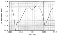
続いて、図22に示したアンテナ装置に対して前述したスロット2117を設け、当該スロット2117のスロット長Lの条件を変更した場合における、アンテナ素子2111aの放射パターンのシミュレーション結果の一例について説明する。なお、スロット2117については、図9を参照して説明した例と同様に、アンテナ素子2111aと、アンテナ素子2111b及び2111cのそれぞれと、の間に設けるものとする。また、スロット位置については、互いに隣り合うアンテナ素子2111間の中心とする。また、素子間隔dについては、d=5mmとする。また、アンテナ素子2111aとしては、比較例1に係るアンテナ素子2111と同様のものを適用するものとする。(Example 1-1: Study on slot length)
Next, an example of a simulation result of the radiation pattern of the
ここで、(式1)及び(式2)として前述したスロット長Lの条件を鑑みると、スロット長Lは、L>λg/2=3.65mmの条件を満たすことがより望ましい。そこで、L=4.2mmの場合(L>3.65mmの場合)、L=3.65mmの場合、及びL=3.6mmの場合(L<3.65mmの場合)のそれぞれについて、アンテナ素子2111aの放射パターンのシミュレーションを行った。Here, considering the condition of the slot length L described above as (Equation 1) and (Equation 2), it is more preferable that the slot length L satisfies the condition of L> λ g /2=3.65 mm. Therefore, for each of L = 4.2 mm (L> 3.65 mm), L = 3.65 mm, and L = 3.6 mm (L <3.65 mm), the antenna element A simulation of the radiation pattern of 2111a was performed.
図25〜図27は、実施例1に係るアンテナ装置におけるスロット長の条件に応じた放射パターンのシミュレーション結果の一例を示した図である。具体的には、図25〜図27については、給電点2113への給電に伴い生じるアンテナ素子2111aの放射パターンをphi90面で切断した場合における当該放射パターンの一例を示している。より具体的には、図25は、スロット長L=4.2mmとした場合におけるアンテナ素子2111aの放射パターンのシミュレーション結果の一例を示している。また、図26は、スロット長L=3.65mmとした場合におけるアンテナ素子2111aの放射パターンのシミュレーション結果の一例を示している。また、図27は、スロット長L=3.6mmとした場合におけるアンテナ素子2111aの放射パターンのシミュレーション結果の一例を示している。なお、図25〜図27の縦軸及び横軸は、図20と同様である。
FIGS. 25 to 27 are diagrams illustrating an example of a simulation result of a radiation pattern according to the condition of the slot length in the antenna device according to the first embodiment. More specifically, FIGS. 25 to 27 show an example of the radiation pattern when the radiation pattern of the
図25と図24とを比較するとわかるように、スロット2117が設けられることで、スロット2117が設けられていない場合に比べて、アンテナの放射パターンのうち極小値に相当する部分の特性が改善されていることがわかる。
As can be seen from a comparison between FIG. 25 and FIG. 24, the provision of the
また、図25と図26及び図27のそれぞれとを比較するとわかるように、図25に示した(式1)及び(式2)の条件を満たす場合のシミュレーション結果については、図26及び図27に示した当該条件を満たさない場合のシミュレーション結果よりも歪が改善されている。特に、図26に示した、L=λg/2=3.65mmの場合の例については、アンテナ素子2111aとスロット2117との結合がより強くなり、却って歪が大きくなっていることがわかる。As can be seen by comparing FIG. 25 with FIGS. 26 and 27, the simulation results when the conditions of (Equation 1) and (Equation 2) shown in FIG. 25 are satisfied are shown in FIGS. 26 and 27. The distortion is improved as compared with the simulation result in the case where the above condition is not satisfied. In particular, in the example where L = λ g /2=3.65 mm shown in FIG. 26, it can be seen that the coupling between the
以上、図22に示したアンテナ装置に対して前述したスロット2117を設け、当該スロット2117のスロット長Lの条件を変更した場合における、アンテナ素子2111aの放射パターンのシミュレーション結果の一例について説明した。
The example of the simulation result of the radiation pattern of the
(実施例1−2:素子間隔に関する検討)
続いて、図22に示したアンテナ装置において、互いに隣り合う2つのアンテナ素子2111間の素子間隔dの条件を変更した場合における、アンテナ素子2111aの放射パターンのシミュレーション結果の一例について説明する。なお、本説明において、スロット2117については設けずに、素子間隔dの条件のみを変更するものとする。また、アンテナ素子2111aとしては、比較例1に係るアンテナ素子2111と同様のものを適用するものとする。(Example 1-2: Study on element spacing)
Next, an example of a simulation result of the radiation pattern of the
ここで、(式3)として前述した素子間隔dの条件を鑑みると、無線信号の波長λ0=10.7mmとなるため、素子間隔dは、5.4mmm≦d<10.7mmの条件を満たすことがより望ましい。なお、前述したように、素子間隔dの上限側については、グレーティングローブの発生条件に応じて決定されている。そこで、本説明では、主に下限側の境界値を基点とした条件に着目した放射パターンのシミュレーションの一例について説明する。具体的には、素子間隔d=6.0mmの場合(5.4mm<d<10.7mmの場合)、d=5.4mmの場合、及びd=4.0mmの場合(d<5.4mmの場合)のそれぞれについて、アンテナ素子2111aの放射パターンのシミュレーションを行った。Here, considering the condition of the element spacing d described above as (Equation 3), since the wavelength λ 0 of the wireless signal is 10.7 mm, the condition of the element spacing d is 5.4 mm mm ≦ d <10.7 mm. It is more desirable to satisfy. As described above, the upper limit of the element interval d is determined according to the conditions for generating the grating lobe. Therefore, in the present description, an example of a radiation pattern simulation mainly focusing on a condition based on the lower limit side boundary value will be described. More specifically, when the element spacing d = 6.0 mm (5.4 mm <d <10.7 mm), d = 5.4 mm, and when d = 4.0 mm (d <5.4 mm) In each case, the radiation pattern of the
図28〜30は、実施例1に係るアンテナ装置における素子間隔の条件に応じた放射パターンのシミュレーション結果の一例を示している。具体的には、図28〜図30は、給電点2114への給電に伴い生じるアンテナ素子2111aの放射パターンをphi90面で切断した場合における当該放射パターンの一例を示している。より具体的には、図28は、素子間隔d=6.0mmとした場合におけるアンテナ素子2111aの放射パターンのシミュレーション結果の一例を示している。また、図29は、素子間隔d=5.4mmとした場合におけるアンテナ素子2111aの放射パターンのシミュレーション結果の一例を示している。また、図30は、素子間隔d=4.0mmとした場合におけるアンテナ素子2111aの放射パターンのシミュレーション結果の一例を示している。なお、図28〜図30の縦軸及び横軸は、図20と同様である。
FIGS. 28 to 30 show an example of a simulation result of a radiation pattern according to the condition of the element spacing in the antenna device according to the first embodiment. More specifically, FIGS. 28 to 30 show an example of the radiation pattern when the radiation pattern of the
図28と図23とを比較するとわかるように、素子間隔dを、5.4mm≦d<10.7mmの条件を満たすように設定することで、放射パターンに生じた歪が改善されていることがわかる。 As can be seen from a comparison between FIG. 28 and FIG. 23, distortion generated in the radiation pattern is improved by setting the element interval d so as to satisfy the condition of 5.4 mm ≦ d <10.7 mm. I understand.
また、図28及び図29のそれぞれと図30とを比較するとわかるように、図28及び図29に示した(式3)の条件を満たす場合のシミュレーション結果については、図30に示した当該条件を満たさない場合のシミュレーション結果よりも歪が改善されている。特に、図30に示す例については、図24に示す例に比べて、歪の幅が広がっていることがわかる。 Also, as can be seen by comparing FIG. 28 and FIG. 29 with FIG. 30, the simulation results when the condition of (Equation 3) shown in FIG. 28 and FIG. Are better than the simulation result when the condition is not satisfied. In particular, it can be seen that the example shown in FIG. 30 has a wider range of distortion than the example shown in FIG.
以上、図22に示したアンテナ装置において、互いに隣り合う2つのアンテナ素子2111間の素子間隔dの条件を変更した場合における、アンテナ素子2111aの放射パターンのシミュレーション結果の一例について説明した。
The example of the simulation result of the radiation pattern of the
(実施例1−3:スロット位置に関する検討)
続いて、図22に示したアンテナ装置に対して前述したスロット2117を設け、当該スロット2117のスロット位置(即ち、アンテナ素子2111aとの間の距離p)の条件を変更した場合における、アンテナ素子2111aの放射パターンのシミュレーション結果の一例について説明する。なお、スロット2117については、図9を参照して説明した例と同様に、アンテナ素子2111aと、アンテナ素子2111b及び2111cのそれぞれと、の間に設けるものとする。また、スロット長Lについては、L=4.0mmに設定するものとする。また、素子間隔dについては、d=5mmに設定するものとする。また、アンテナ素子2111aとしては、比較例1に係るアンテナ素子2111と同様のものを適用するものとする。(Example 1-3: Study on slot position)
Subsequently, the above-described
ここで、(式6)として前述した距離p(即ち、スロット位置)の条件を鑑みると、以下に(式7)として示す条件が成り立つ。そのため、距離pは、1.47mm<p<3.53mmの条件を満たすことがより望ましい。 Here, in consideration of the condition of the distance p (that is, the slot position) described above as (Equation 6), the condition shown below as (Equation 7) is satisfied. Therefore, it is more desirable that the distance p satisfies the condition of 1.47 mm <p <3.53 mm.
なお、距離pの上限値側については、スロット2117が第2のアンテナ素子2111bまたは2111cのエッジに掛かる直前の位置に相当する。距離pが上限値を示す場合における第2のアンテナ素子2111bまたは2111cへの影響については、距離pが下限値を示す場合における第1のアンテナ素子2111aへの影響と同様である。そこで、本説明では、主に下限側の境界値を基点とした条件に着目した放射パターンのシミュレーションの一例について説明する。具体的には、距離p=2.8mmの場合(1.47mm<p<3.53mmの場合)、p=1.47mmの場合、及びp=1.4mmの場合(p<1.47mmの場合)のそれぞれについて、アンテナ素子2111aの放射パターンのシミュレーションを行った。
Note that the upper limit of the distance p corresponds to the position immediately before the
図31〜33は、実施例1に係るアンテナ装置におけるスロット位置の条件に応じた放射パターンのシミュレーション結果の一例を示している。具体的には、図31〜図33は、給電点2113への給電に伴い生じるアンテナ素子2111aの放射パターンをphi90面で切断した場合における当該放射パターンの一例を示している。より具体的には、図31は、距離p=2.8mmとした場合におけるアンテナ素子2111aの放射パターンのシミュレーション結果の一例を示している。また、図32は、距離p=1.47mmとした場合におけるアンテナ素子2111aの放射パターンのシミュレーション結果の一例を示している。また、図33は、距離p=1.4mmとした場合におけるアンテナ素子2111aの放射パターンのシミュレーション結果の一例を示している。なお、図31〜図33の縦軸及び横軸は、図20と同様である。
FIGS. 31 to 33 illustrate an example of a simulation result of a radiation pattern according to the condition of the slot position in the antenna device according to the first embodiment. Specifically, FIG. 31 to FIG. 33 show an example of the radiation pattern when the radiation pattern of the
図31と図24とを比較するとわかるように、距離pを、1.47mm<p<3.53mmの条件を満たすように設定することで、放射パターンに生じた歪が改善されている As can be seen from a comparison between FIG. 31 and FIG. 24, the distortion generated in the radiation pattern is improved by setting the distance p so as to satisfy the condition of 1.47 mm <p <3.53 mm.
また、図32及び図33については、スロット2117がアンテナ素子2111aのエッジに掛かるか、もしくはスロット2117がアンテナ素子2111aの平面状のエレメント2112の下部に設けられることとなる。このような状況下では、スロット2117が設けられることで、アンテナ素子2111aのエレメント2112とグランド板2116との間に生じる電界が乱され、アンテナ特性に影響を与えることが推測される。そのため、例えば、図32及び図33に示す例では、アンテナ素子2111aの放射パターンに歪が生じている。
32 and 33, the
以上、図22に示したアンテナ装置に対して前述したスロット2117を設け、当該スロット2117のスロット位置の条件を変更した場合における、アンテナ素子2111aの放射パターンのシミュレーション結果の一例について説明した。
The example of the simulation result of the radiation pattern of the
<3.4.応用例>
続いて、本開示の一実施形態に係るアンテナ装置を適用した通信装置の応用例として、スマートフォンのような通信端末以外の装置に対して、本開示に係る技術を応用する場合の一例について説明する。<3.4. Application>
Subsequently, as an application example of the communication device to which the antenna device according to an embodiment of the present disclosure is applied, an example in which the technology according to the present disclosure is applied to a device other than a communication terminal such as a smartphone will be described. .
近年では、IoT(Internet of Things)と呼ばれる、多様なモノをネットワークにつなげる技術が注目されており、スマートフォンやタブレット端末以外の装置についても、通信に利用可能となる場合が想定される。そのため、例えば、移動可能に構成された各種装置に対して、本開示に係る技術を応用することで、当該装置についても、ミリ波を利用した通信が可能となり、当該通信において偏波MIMOを利用することも可能となる。 In recent years, a technology called IoT (Internet of Things) for connecting various things to a network has attracted attention, and it is assumed that devices other than smartphones and tablet terminals can be used for communication. Therefore, for example, by applying the technology according to the present disclosure to various devices that are configured to be movable, communication using millimeter waves is also possible for the device, and polarization MIMO is used in the communication. It is also possible to do.
例えば、図34は、本実施形態に係る通信装置の応用例について説明するための説明図であり、本開示に係る技術をカメラデバイスに応用した場合の一例を示している。具体的には、図34に示す例では、カメラデバイス300の筐体の外面のうち、互いに異なる方向を向いた面301及び302それぞれの近傍に位置するように、本開示の一実施形態に係るアンテナ装置が保持されている。例えば、参照符号311は、本開示の一実施形態に係るアンテナ装置を模式的に示している。このような構成により、図34に示すカメラデバイス300は、例えば、面301及び302それぞれについて、当該面の法線方向と略一致する方向に伝搬し、かつ偏波方向が互いに異なる複数の偏波それぞれを送信または受信することが可能となる。なお、図34に示した面301及び302のみに限らず、他の面にもアンテナ装置311が設けられていてもよいことは言うまでもない。
For example, FIG. 34 is an explanatory diagram for describing an application example of the communication device according to the present embodiment, and illustrates an example in which the technology according to the present disclosure is applied to a camera device. More specifically, in the example illustrated in FIG. 34, according to an embodiment of the present disclosure, the outer surface of the housing of the
また、本開示に係る技術は、ドローンと呼ばれる無人航空機等にも応用することが可能である。例えば、図35は、本実施形態に係る通信装置の応用例について説明するための説明図であり、本開示に係る技術を、ドローンの下部に設置されるカメラデバイスに応用した場合の一例を示している。具体的には、高所を飛行するドローンの場合には、主に、下方側において各方向から到来する無線信号(ミリ波)を送信または受信できることが望ましい。そのため、例えば、図35に示す例では、ドローンの下部に設置されるカメラデバイス400の筐体の外面401のうち、互いに異なる方向を向いた各部の近傍に位置するように、本開示の一実施形態に係るアンテナ装置が保持されている。例えば、参照符号411は、本開示の一実施形態に係るアンテナ装置を模式的に示している。また、図35では図示を省略しているが、カメラデバイス400のみに限らず、例えば、ドローン自体の筐体の各部にアンテナ装置411が設けられていてもよい。この場合においても、特に、当該筐体の下方側にアンテナ装置411が設けられているとよい。
Further, the technology according to the present disclosure can be applied to an unmanned aerial vehicle called a drone or the like. For example, FIG. 35 is an explanatory diagram for describing an application example of the communication device according to the present embodiment, and illustrates an example in which the technology according to the present disclosure is applied to a camera device installed below a drone. ing. Specifically, in the case of a drone flying at high altitude, it is desirable that a radio signal (millimeter wave) arriving from each direction can be transmitted or received mainly on the lower side. Therefore, for example, in the example illustrated in FIG. 35, one embodiment of the present disclosure is configured such that the
なお、図35に示すように、対象となる装置の筐体の外面のうち少なくとも一部が湾曲する面(即ち、曲面)として構成されている場合においては、当該湾曲する面中における各部分領域のうち、法線方向が互いに交差するか、または、当該法線方向が互いにねじれの位置にある複数の部分領域それぞれの近傍に、アンテナ装置411が保持されるとよい。このような構成により、図35に示すカメラデバイス400は、各部分領域の法線方向と略一致する方向に伝搬し、かつ偏波方向が互いに異なる複数の偏波それぞれを送信または受信することが可能となる。
As shown in FIG. 35, when at least a part of the outer surface of the housing of the target device is configured as a curved surface (that is, a curved surface), each partial area in the curved surface is used. Of these, the
なお、図34及び図35を参照して説明した例はあくまで一例であり、ミリ波を利用した通信を行う装置であれば、本開示に係る技術の応用先は特に限定されない。 The example described with reference to FIGS. 34 and 35 is merely an example, and the application of the technology according to the present disclosure is not particularly limited as long as the device performs communication using millimeter waves.
以上、本開示の一実施形態に係るアンテナ装置を適用した通信装置の応用例として、図34及び図35を参照して、スマートフォンのような通信端末以外の装置に対して、本開示に係る技術を応用する場合の一例について説明した。 As described above, as an application example of the communication device to which the antenna device according to an embodiment of the present disclosure is applied, with reference to FIGS. 34 and 35, the technology according to the present disclosure is applied to a device other than a communication terminal such as a smartphone. An example in which is applied has been described.
<<4.むすび>>
以上説明したように、本実施形態に係るアンテナ装置は、略平面状の誘電体基板と、複数のアンテナ素子と、グランド板とを含む。複数のアンテナ素子は、上記誘電体基板の一方の面上に、当該誘電体基板の平面に対して水平な第1の方向に沿って配設され、それぞれが、偏波方向が互いに異なる第1の無線信号及び第2の無線信号を送信または受信する。グランド板は、上記誘電体基板の他方の面の略全体に設けられ、互いに隣り合う第1のアンテナ素子及び第2のアンテナ素子の間に対応する領域に、前記第1の方向に直交する第2の方向に延伸するように長尺状のスロットが設けられている。また、グランド板に設けられた当該スロットのスロット長Lは、(式1)及び(式2)として前述した条件を満たすように形成される。<< 4. Conclusion >>
As described above, the antenna device according to the present embodiment includes the substantially planar dielectric substrate, the plurality of antenna elements, and the ground plate. The plurality of antenna elements are disposed on one surface of the dielectric substrate along a first direction horizontal to a plane of the dielectric substrate, and each of the first and second antenna elements has a different polarization direction. Or the second wireless signal is transmitted or received. The ground plate is provided on substantially the entire other surface of the dielectric substrate, and is provided in a region corresponding to a space between the first antenna element and the second antenna element adjacent to each other, and a ground plane orthogonal to the first direction. An elongated slot is provided so as to extend in two directions. The slot length L of the slot provided in the ground plate is formed so as to satisfy the conditions described above as (Equation 1) and (Equation 2).
また、上記第1のアンテナ素子及び上記第2のアンテナ素子それぞれの中心間の距離(即ち、素子間隔d)は、(式3)として前述した条件を満たすように形成されてもよい。また、上記第1のアンテナ素子の中心と、上記スロットの中心と、の間の距離p(即ち、スロット位置)は、(式4)〜(式6)として前述した条件を満たすように形成されてもよい。 Further, the distance between the centers of the first antenna element and the second antenna element (that is, the element interval d) may be formed so as to satisfy the condition described above as (Equation 3). The distance p (that is, the slot position) between the center of the first antenna element and the center of the slot is formed so as to satisfy the conditions described above as (Equations 4) to (Equation 6). You may.
以上のような構成により、本実施形態に係るアンテナ装置に依れば、複数のアンテナ素子をアレイ化した場合においても、アンテナ素子の放射パターンとして、より好適な放射パターンを得ることが可能となる。 With the configuration as described above, according to the antenna device according to the present embodiment, even when a plurality of antenna elements are arrayed, a more suitable radiation pattern can be obtained as the radiation pattern of the antenna elements. .
以上、添付図面を参照しながら本開示の好適な実施形態について詳細に説明したが、本開示の技術的範囲はかかる例に限定されない。本開示の技術分野における通常の知識を有する者であれば、特許請求の範囲に記載された技術的思想の範疇内において、各種の変更例または修正例に想到し得ることは明らかであり、これらについても、当然に本開示の技術的範囲に属するものと了解される。 As described above, the preferred embodiments of the present disclosure have been described in detail with reference to the accompanying drawings, but the technical scope of the present disclosure is not limited to such examples. It is apparent that a person having ordinary knowledge in the technical field of the present disclosure can conceive various changes or modifications within the scope of the technical idea described in the claims. It is understood that also belongs to the technical scope of the present disclosure.
また、本明細書に記載された効果は、あくまで説明的または例示的なものであって限定的ではない。つまり、本開示に係る技術は、上記の効果とともに、または上記の効果に代えて、本明細書の記載から当業者には明らかな他の効果を奏しうる。 Further, the effects described in this specification are merely illustrative or exemplary, and are not restrictive. That is, the technology according to the present disclosure can exhibit other effects that are obvious to those skilled in the art from the description in the present specification, in addition to or instead of the above effects.
なお、以下のような構成も本開示の技術的範囲に属する。
(1)
略平面状の誘電体基板と、
前記誘電体基板の一方の面上に、当該誘電体基板の平面に対して水平な第1の方向に沿って配設され、それぞれが、偏波方向が互いに異なる第1の無線信号及び第2の無線信号を送信または受信する複数のアンテナ素子と、
前記誘電体基板の他方の面の略全体に設けられ、互いに隣り合う第1のアンテナ素子及び第2のアンテナ素子の間に対応する領域に、前記第1の方向に直交する第2の方向に延伸するように長尺状のスロットが設けられたグランド板と、
を備え、
前記複数のアンテナ素子それぞれが送信または受信する無線信号の波長をλ0、前記誘電体基板の比誘電率をεr1、前記グランド板に対して前記誘電体基板とは逆側に位置する誘電体の比誘電率をεr2とした場合に、前記スロットの前記第2の方向の長さLが以下に示す条件式を満たす、アンテナ装置。
前記第1のアンテナ素子及び前記第2のアンテナ素子それぞれの中心間の距離dが以下に示す条件式を満たす、前記(1)に記載のアンテナ装置。
前記第1のアンテナ素子の中心と前記スロットとの間の前記第1の方向に沿った距離pが以下に示す条件式を満たす、前記(1)または(2)に記載のアンテナ装置。
前記第1の無線信号は、偏波方向が前記第1の方向と略一致し、
前記第2の無線信号は、偏波方向が前記第2の方向と略一致し、
前記アンテナ素子ごとに、前記第1の無線信号に対応する第1の給電点と、前記第2の無線信号に対応する第2の給電点と、が設けられている、
前記(1)〜(3)のいずれか一項に記載のアンテナ装置。
(5)
前記第2のアンテナ素子における前記第1の給電点は、当該第2のアンテナ素子の前記第1の方向の端部のうち、前記第1のアンテナ素子とは逆側の当該端部の方向に偏心して設けられている、前記(4)に記載のアンテナ装置。
(6)
前記アンテナ素子は、平面アンテナとして構成される、前記(1)〜(5)のいずれか一項に記載のアンテナ装置。
(7)
それぞれが前記誘電体基板、前記複数のアンテナ素子、及び前記グランド板を含む第1のアンテナ部及び第2のアンテナ部を備え、
前記第1のアンテナ部と前記第2のアンテナ部とは、所定の筐体に対して、それぞれの法線方向が互いに交差するか、または、当該法線方向が互いにねじれの位置にあるように保持される、前記(1)〜(6)のいずれか一項に記載のアンテナ装置。
(8)
前記第1のアンテナ部の前記第1の方向に延伸する端部と、前記第2のアンテナ部の前記第1の方向に延伸する端部と、を連結する連結部を備える、前記(7)に記載のアンテナ装置。Note that the following configuration also belongs to the technical scope of the present disclosure.
(1)
A substantially planar dielectric substrate;
A first radio signal and a second radio signal are disposed on one surface of the dielectric substrate along a first direction that is horizontal to a plane of the dielectric substrate. A plurality of antenna elements for transmitting or receiving a wireless signal,
It is provided on substantially the other surface of the dielectric substrate and in a region corresponding to a space between the first antenna element and the second antenna element adjacent to each other, in a second direction orthogonal to the first direction. A ground plate provided with a long slot so as to extend,
With
The wavelength of the radio signal transmitted or received by each of the plurality of antenna elements is λ 0 , the relative permittivity of the dielectric substrate is ε r1 , and the dielectric located on the opposite side of the ground substrate to the dielectric substrate An antenna device, wherein a length L of the slot in the second direction satisfies the following conditional expression, where ε r2 is a relative dielectric constant of the slot.
The antenna device according to (1), wherein a distance d between the centers of the first antenna element and the second antenna element satisfies the following conditional expression.
The antenna device according to (1) or (2), wherein a distance p along the first direction between the center of the first antenna element and the slot satisfies the following conditional expression.
The first wireless signal has a polarization direction substantially coinciding with the first direction,
The second wireless signal has a polarization direction substantially coinciding with the second direction,
A first feed point corresponding to the first wireless signal and a second feed point corresponding to the second wireless signal are provided for each antenna element.
The antenna device according to any one of (1) to (3).
(5)
The first feeding point of the second antenna element is directed to the end of the second antenna element in the first direction that is opposite to the first antenna element. The antenna device according to (4), which is eccentrically provided.
(6)
The antenna device according to any one of (1) to (5), wherein the antenna element is configured as a planar antenna.
(7)
Each comprising a first antenna unit and a second antenna unit including the dielectric substrate, the plurality of antenna elements, and the ground plate,
The first antenna unit and the second antenna unit may be arranged such that their normal directions intersect with each other with respect to a predetermined casing, or that the normal directions are in mutually twisted positions. The antenna device according to any one of (1) to (6), which is held.
(8)
(7) including a connecting portion that connects an end portion of the first antenna portion extending in the first direction and an end portion of the second antenna portion extending in the first direction. An antenna device according to
1 システム
100 基地局
200 端末装置
2001 アンテナ部
2003 無線通信部
2005 通信制御部
2007 記憶部
211 通信装置
2110 アンテナ装置
2111 アンテナ素子
2112 エレメント
2113、2114 給電点
2115 誘電体基板
2116 グランド板
2117 スロット
Claims (8)
前記誘電体基板の一方の面上に、当該誘電体基板の平面に対して水平な第1の方向に沿って配設され、それぞれが、偏波方向が互いに異なる第1の無線信号及び第2の無線信号を送信または受信する複数のアンテナ素子と、
前記誘電体基板の他方の面の略全体に設けられ、互いに隣り合う第1のアンテナ素子及び第2のアンテナ素子の間に対応する領域に、前記第1の方向に直交する第2の方向に延伸するように長尺状のスロットが設けられたグランド板と、
を備え、
前記複数のアンテナ素子それぞれが送信または受信する無線信号の波長をλ0、前記誘電体基板の比誘電率をεr1、前記グランド板に対して前記誘電体基板とは逆側に位置する誘電体の比誘電率をεr2とした場合に、前記スロットの前記第2の方向の長さLが以下に示す条件式を満たす、アンテナ装置。
A first radio signal and a second radio signal are disposed on one surface of the dielectric substrate along a first direction that is horizontal to a plane of the dielectric substrate. A plurality of antenna elements for transmitting or receiving a wireless signal,
It is provided on substantially the other surface of the dielectric substrate and in a region corresponding to a space between the first antenna element and the second antenna element adjacent to each other, in a second direction orthogonal to the first direction. A ground plate provided with a long slot so as to extend,
With
The wavelength of the radio signal transmitted or received by each of the plurality of antenna elements is λ 0 , the relative permittivity of the dielectric substrate is ε r1 , and the dielectric located on the opposite side of the ground substrate to the dielectric substrate An antenna device, wherein a length L of the slot in the second direction satisfies the following conditional expression, where ε r2 is a relative dielectric constant of the slot.
前記第2の無線信号は、偏波方向が前記第2の方向と略一致し、
前記アンテナ素子ごとに、前記第1の無線信号に対応する第1の給電点と、前記第2の無線信号に対応する第2の給電点と、が設けられている、
請求項1に記載のアンテナ装置。The first wireless signal has a polarization direction substantially coinciding with the first direction,
The second wireless signal has a polarization direction substantially coinciding with the second direction,
A first feed point corresponding to the first wireless signal and a second feed point corresponding to the second wireless signal are provided for each antenna element.
The antenna device according to claim 1.
前記第1のアンテナ部と前記第2のアンテナ部とは、所定の筐体に対して、それぞれの法線方向が互いに交差するか、または、当該法線方向が互いにねじれの位置にあるように保持される、請求項1に記載のアンテナ装置。Each comprising a first antenna unit and a second antenna unit including the dielectric substrate, the plurality of antenna elements, and the ground plate,
The first antenna unit and the second antenna unit may be arranged such that their normal directions cross each other with respect to a predetermined housing, or that the normal directions are twisted with each other. The antenna device according to claim 1, which is held.
Applications Claiming Priority (3)
| Application Number | Priority Date | Filing Date | Title |
|---|---|---|---|
| JP2017116760 | 2017-06-14 | ||
| JP2017116760 | 2017-06-14 | ||
| PCT/JP2018/005297 WO2018230039A1 (en) | 2017-06-14 | 2018-02-15 | Antenna device |
Publications (2)
| Publication Number | Publication Date |
|---|---|
| JPWO2018230039A1 true JPWO2018230039A1 (en) | 2020-04-02 |
| JP6850993B2 JP6850993B2 (en) | 2021-03-31 |
Family
ID=64660594
Family Applications (1)
| Application Number | Title | Priority Date | Filing Date |
|---|---|---|---|
| JP2019525071A Expired - Fee Related JP6850993B2 (en) | 2017-06-14 | 2018-02-15 | Antenna device |
Country Status (5)
| Country | Link |
|---|---|
| US (1) | US11075462B2 (en) |
| EP (1) | EP3641060B1 (en) |
| JP (1) | JP6850993B2 (en) |
| CN (1) | CN110870138B (en) |
| WO (1) | WO2018230039A1 (en) |
Families Citing this family (21)
| Publication number | Priority date | Publication date | Assignee | Title |
|---|---|---|---|---|
| US11239571B2 (en) | 2017-10-19 | 2022-02-01 | Sony Corporation | Antenna device |
| WO2020027058A1 (en) * | 2018-08-02 | 2020-02-06 | 株式会社村田製作所 | Antenna device |
| WO2020031776A1 (en) * | 2018-08-06 | 2020-02-13 | 株式会社村田製作所 | Antenna module |
| CN109449568B (en) * | 2018-08-07 | 2020-09-18 | 瑞声科技(新加坡)有限公司 | Millimeter wave array antenna and mobile terminal |
| KR102621852B1 (en) | 2018-12-26 | 2024-01-08 | 삼성전자주식회사 | Antenna structure including conductive patch feeded using muitiple electrical path and electronic device including the antenna structure |
| CN110011071A (en) * | 2018-12-28 | 2019-07-12 | 瑞声科技(新加坡)有限公司 | Mobile terminal antenna system, mobile terminal |
| JP6773259B1 (en) * | 2019-02-20 | 2020-10-21 | 株式会社村田製作所 | Antenna module, communication device equipped with it, and manufacturing method of antenna module |
| CN109755743B (en) * | 2019-03-11 | 2021-06-01 | 青岛海信移动通信技术股份有限公司 | Antenna and terminal |
| CN111725605B (en) * | 2019-03-20 | 2022-03-15 | Oppo广东移动通信有限公司 | Millimeter wave module and electronic equipment |
| US12046814B2 (en) | 2019-05-30 | 2024-07-23 | Sony Interactive Entertainment Inc. | Antenna unit and communication equipment |
| CN112290234A (en) * | 2019-07-24 | 2021-01-29 | 台达电子工业股份有限公司 | communication device |
| JP6971350B2 (en) * | 2020-03-17 | 2021-11-24 | ソフトバンク株式会社 | Antenna device, wireless communication device and mobile body |
| TWM600485U (en) * | 2020-05-13 | 2020-08-21 | 和碩聯合科技股份有限公司 | Antenna module |
| CN111740217B (en) * | 2020-07-03 | 2021-07-23 | 维沃移动通信有限公司 | An antenna assembly and electronic device |
| JP7591393B2 (en) * | 2020-12-10 | 2024-11-28 | ニデックプレシジョン株式会社 | Imaging device and program |
| CN112768928A (en) * | 2020-12-30 | 2021-05-07 | Oppo广东移动通信有限公司 | Antenna assembly and electronic equipment |
| US20240405432A1 (en) | 2021-02-03 | 2024-12-05 | Dai Nippon Printing Co., Ltd. | Antenna and communication apparatus |
| CN115552728B (en) * | 2021-04-29 | 2025-04-18 | 京东方科技集团股份有限公司 | Antenna and preparation method thereof, antenna system |
| EP4315511A4 (en) | 2021-07-16 | 2024-08-21 | Samsung Electronics Co., Ltd. | Wide scanning patch antenna array |
| JP7518447B1 (en) * | 2023-06-09 | 2024-07-18 | 横浜ゴム株式会社 | Drone equipped with a communications antenna, and surveillance system and surveillance method using this drone |
| WO2026004663A1 (en) * | 2024-06-26 | 2026-01-02 | ソニーセミコンダクタソリューションズ株式会社 | Antenna and antenna system |
Citations (4)
| Publication number | Priority date | Publication date | Assignee | Title |
|---|---|---|---|---|
| JPH10200326A (en) * | 1997-01-07 | 1998-07-31 | Mitsubishi Electric Corp | Antenna device |
| US20020122006A1 (en) * | 2001-03-05 | 2002-09-05 | Magis Networks, Inc. | Conformal box antenna |
| US20030193437A1 (en) * | 2002-04-11 | 2003-10-16 | Nokia Corporation | Method and system for improving isolation in radio-frequency antennas |
| JP2005072653A (en) * | 2003-08-25 | 2005-03-17 | Ntt Docomo Inc | Transmit / receive separation type microstrip antenna |
Family Cites Families (9)
| Publication number | Priority date | Publication date | Assignee | Title |
|---|---|---|---|---|
| DE60009520T2 (en) * | 1999-09-14 | 2005-03-03 | Paratek Microwave, Inc. | SERIES-SPREADED PHASERARRAY ANTENNAS WITH DIELECTRIC PHASE SLIDES |
| US6239762B1 (en) * | 2000-02-02 | 2001-05-29 | Lockheed Martin Corporation | Interleaved crossed-slot and patch array antenna for dual-frequency and dual polarization, with multilayer transmission-line feed network |
| JP3842645B2 (en) * | 2001-12-27 | 2006-11-08 | 日本電波工業株式会社 | Multi-element array type planar antenna |
| JP2007142876A (en) | 2005-11-18 | 2007-06-07 | Ntt Docomo Inc | Polarized patch antenna |
| US7999745B2 (en) * | 2007-08-15 | 2011-08-16 | Powerwave Technologies, Inc. | Dual polarization antenna element with dielectric bandwidth compensation and improved cross-coupling |
| CN101316008B (en) | 2008-06-13 | 2012-06-27 | 哈尔滨工业大学 | Multiple Antennas for MIMO Mobile Terminals with High Isolation and Low Correlation |
| US9742077B2 (en) * | 2011-03-15 | 2017-08-22 | Intel Corporation | Mm-wave phased array antenna with beam tilting radiation pattern |
| EP2575211B1 (en) * | 2011-09-27 | 2014-11-05 | Technische Universität Darmstadt | Electronically steerable planar phased array antenna |
| US9755306B1 (en) * | 2013-01-07 | 2017-09-05 | Lockheed Martin Corporation | Wideband antenna design for wide-scan low-profile phased arrays |
-
2018
- 2018-02-15 WO PCT/JP2018/005297 patent/WO2018230039A1/en not_active Ceased
- 2018-02-15 CN CN201880046521.7A patent/CN110870138B/en active Active
- 2018-02-15 EP EP18817484.1A patent/EP3641060B1/en active Active
- 2018-02-15 JP JP2019525071A patent/JP6850993B2/en not_active Expired - Fee Related
- 2018-02-15 US US16/619,968 patent/US11075462B2/en active Active
Patent Citations (4)
| Publication number | Priority date | Publication date | Assignee | Title |
|---|---|---|---|---|
| JPH10200326A (en) * | 1997-01-07 | 1998-07-31 | Mitsubishi Electric Corp | Antenna device |
| US20020122006A1 (en) * | 2001-03-05 | 2002-09-05 | Magis Networks, Inc. | Conformal box antenna |
| US20030193437A1 (en) * | 2002-04-11 | 2003-10-16 | Nokia Corporation | Method and system for improving isolation in radio-frequency antennas |
| JP2005072653A (en) * | 2003-08-25 | 2005-03-17 | Ntt Docomo Inc | Transmit / receive separation type microstrip antenna |
Non-Patent Citations (1)
| Title |
|---|
| J.OUYANG ET AL.: ""Reducing Mutual Coupling of Closely Spaced Microstrip MIMO Antennas for WLAN Application"", IEEE ANTENNAS AND WIRELESS PROPAGATION LETTERS, vol. 10, JPN6020043157, 2011, pages 310 - 313, ISSN: 0004384606 * |
Also Published As
| Publication number | Publication date |
|---|---|
| EP3641060B1 (en) | 2021-11-24 |
| US11075462B2 (en) | 2021-07-27 |
| CN110870138A (en) | 2020-03-06 |
| EP3641060A4 (en) | 2020-06-24 |
| JP6850993B2 (en) | 2021-03-31 |
| CN110870138B (en) | 2021-08-17 |
| WO2018230039A1 (en) | 2018-12-20 |
| EP3641060A1 (en) | 2020-04-22 |
| US20200144729A1 (en) | 2020-05-07 |
Similar Documents
| Publication | Publication Date | Title |
|---|---|---|
| JP6850993B2 (en) | Antenna device | |
| JP6988909B2 (en) | Antenna device | |
| ES2925455T3 (en) | High-gain, wide-bandwidth antenna incorporating a differential feed scheme | |
| JP6919730B2 (en) | Antenna device | |
| CN110383583B (en) | Communication device | |
| CA2807722C (en) | Compact radiation structure for diversity antennas | |
| WO2014005436A1 (en) | Quadri-polarized aerial oscillator, quadri-polarized aerial and quadri-polarized multi-aerial array | |
| US10148014B2 (en) | Highly isolated monopole antenna system | |
| US20230299491A1 (en) | Antenna module and manufacturing method thereof | |
| US12191564B2 (en) | Transmit-receive isolation for a dual-polarized MIMO antenna array | |
| CN106992802B (en) | Signal receiving and transmitting device for user terminal, user terminal and signal transmission method | |
| US20170054198A1 (en) | Multi-element telecommunications antenna | |
| Balling et al. | Broadband dual polarized antenna arrays for mobile communication applications | |
| Patel et al. | Antenna Bandwidth Improvement for CoMP System |
Legal Events
| Date | Code | Title | Description |
|---|---|---|---|
| A621 | Written request for application examination |
Free format text: JAPANESE INTERMEDIATE CODE: A621 Effective date: 20191203 |
|
| A131 | Notification of reasons for refusal |
Free format text: JAPANESE INTERMEDIATE CODE: A131 Effective date: 20201110 |
|
| A521 | Request for written amendment filed |
Free format text: JAPANESE INTERMEDIATE CODE: A523 Effective date: 20210108 |
|
| TRDD | Decision of grant or rejection written | ||
| A01 | Written decision to grant a patent or to grant a registration (utility model) |
Free format text: JAPANESE INTERMEDIATE CODE: A01 Effective date: 20210202 |
|
| A61 | First payment of annual fees (during grant procedure) |
Free format text: JAPANESE INTERMEDIATE CODE: A61 Effective date: 20210303 |
|
| A61 | First payment of annual fees (during grant procedure) |
Free format text: JAPANESE INTERMEDIATE CODE: A61 Effective date: 20210215 |
|
| R151 | Written notification of patent or utility model registration |
Ref document number: 6850993 Country of ref document: JP Free format text: JAPANESE INTERMEDIATE CODE: R151 |
|
| LAPS | Cancellation because of no payment of annual fees |