JPWO2017182910A1 - Semiconductor device and manufacturing method of semiconductor device - Google Patents
Semiconductor device and manufacturing method of semiconductor device Download PDFInfo
- Publication number
- JPWO2017182910A1 JPWO2017182910A1 JP2018512507A JP2018512507A JPWO2017182910A1 JP WO2017182910 A1 JPWO2017182910 A1 JP WO2017182910A1 JP 2018512507 A JP2018512507 A JP 2018512507A JP 2018512507 A JP2018512507 A JP 2018512507A JP WO2017182910 A1 JPWO2017182910 A1 JP WO2017182910A1
- Authority
- JP
- Japan
- Prior art keywords
- insulator
- oxide
- conductor
- transistor
- film
- Prior art date
- Legal status (The legal status is an assumption and is not a legal conclusion. Google has not performed a legal analysis and makes no representation as to the accuracy of the status listed.)
- Granted
Links
Images


Classifications
-
- H—ELECTRICITY
- H10—SEMICONDUCTOR DEVICES; ELECTRIC SOLID-STATE DEVICES NOT OTHERWISE PROVIDED FOR
- H10P—GENERIC PROCESSES OR APPARATUS FOR THE MANUFACTURE OR TREATMENT OF DEVICES COVERED BY CLASS H10
- H10P30/00—Ion implantation into wafers, substrates or parts of devices
- H10P30/40—Ion implantation into wafers, substrates or parts of devices into insulating materials
-
- H—ELECTRICITY
- H01—ELECTRIC ELEMENTS
- H01J—ELECTRIC DISCHARGE TUBES OR DISCHARGE LAMPS
- H01J37/00—Discharge tubes with provision for introducing objects or material to be exposed to the discharge, e.g. for the purpose of examination or processing thereof
- H01J37/32—Gas-filled discharge tubes
- H01J37/32009—Arrangements for generation of plasma specially adapted for examination or treatment of objects, e.g. plasma sources
- H01J37/32192—Microwave generated discharge
-
- H—ELECTRICITY
- H10—SEMICONDUCTOR DEVICES; ELECTRIC SOLID-STATE DEVICES NOT OTHERWISE PROVIDED FOR
- H10B—ELECTRONIC MEMORY DEVICES
- H10B99/00—Subject matter not provided for in other groups of this subclass
- H10B99/22—Subject matter not provided for in other groups of this subclass including field-effect components
-
- H—ELECTRICITY
- H10—SEMICONDUCTOR DEVICES; ELECTRIC SOLID-STATE DEVICES NOT OTHERWISE PROVIDED FOR
- H10D—INORGANIC ELECTRIC SEMICONDUCTOR DEVICES
- H10D30/00—Field-effect transistors [FET]
- H10D30/60—Insulated-gate field-effect transistors [IGFET]
- H10D30/67—Thin-film transistors [TFT]
-
- H—ELECTRICITY
- H10—SEMICONDUCTOR DEVICES; ELECTRIC SOLID-STATE DEVICES NOT OTHERWISE PROVIDED FOR
- H10D—INORGANIC ELECTRIC SEMICONDUCTOR DEVICES
- H10D30/00—Field-effect transistors [FET]
- H10D30/60—Insulated-gate field-effect transistors [IGFET]
- H10D30/67—Thin-film transistors [TFT]
- H10D30/6704—Thin-film transistors [TFT] having supplementary regions or layers in the thin films or in the insulated bulk substrates for controlling properties of the device
-
- H—ELECTRICITY
- H10—SEMICONDUCTOR DEVICES; ELECTRIC SOLID-STATE DEVICES NOT OTHERWISE PROVIDED FOR
- H10D—INORGANIC ELECTRIC SEMICONDUCTOR DEVICES
- H10D30/00—Field-effect transistors [FET]
- H10D30/60—Insulated-gate field-effect transistors [IGFET]
- H10D30/67—Thin-film transistors [TFT]
- H10D30/6729—Thin-film transistors [TFT] characterised by the electrodes
- H10D30/673—Thin-film transistors [TFT] characterised by the electrodes characterised by the shapes, relative sizes or dispositions of the gate electrodes
- H10D30/6733—Multi-gate TFTs
- H10D30/6734—Multi-gate TFTs having gate electrodes arranged on both top and bottom sides of the channel, e.g. dual-gate TFTs
-
- H—ELECTRICITY
- H10—SEMICONDUCTOR DEVICES; ELECTRIC SOLID-STATE DEVICES NOT OTHERWISE PROVIDED FOR
- H10D—INORGANIC ELECTRIC SEMICONDUCTOR DEVICES
- H10D30/00—Field-effect transistors [FET]
- H10D30/60—Insulated-gate field-effect transistors [IGFET]
- H10D30/67—Thin-film transistors [TFT]
- H10D30/674—Thin-film transistors [TFT] characterised by the active materials
- H10D30/6755—Oxide semiconductors, e.g. zinc oxide, copper aluminium oxide or cadmium stannate
-
- H—ELECTRICITY
- H10—SEMICONDUCTOR DEVICES; ELECTRIC SOLID-STATE DEVICES NOT OTHERWISE PROVIDED FOR
- H10D—INORGANIC ELECTRIC SEMICONDUCTOR DEVICES
- H10D30/00—Field-effect transistors [FET]
- H10D30/60—Insulated-gate field-effect transistors [IGFET]
- H10D30/67—Thin-film transistors [TFT]
- H10D30/6757—Thin-film transistors [TFT] characterised by the structure of the channel, e.g. transverse or longitudinal shape or doping profile
-
- H—ELECTRICITY
- H10—SEMICONDUCTOR DEVICES; ELECTRIC SOLID-STATE DEVICES NOT OTHERWISE PROVIDED FOR
- H10D—INORGANIC ELECTRIC SEMICONDUCTOR DEVICES
- H10D64/00—Electrodes of devices having potential barriers
- H10D64/01—Manufacture or treatment
- H10D64/011—Manufacture or treatment of electrodes ohmically coupled to a semiconductor
-
- H—ELECTRICITY
- H10—SEMICONDUCTOR DEVICES; ELECTRIC SOLID-STATE DEVICES NOT OTHERWISE PROVIDED FOR
- H10D—INORGANIC ELECTRIC SEMICONDUCTOR DEVICES
- H10D86/00—Integrated devices formed in or on insulating or conducting substrates, e.g. formed in silicon-on-insulator [SOI] substrates or on stainless steel or glass substrates
- H10D86/01—Manufacture or treatment
- H10D86/021—Manufacture or treatment of multiple TFTs
- H10D86/0221—Manufacture or treatment of multiple TFTs comprising manufacture, treatment or patterning of TFT semiconductor bodies
-
- H—ELECTRICITY
- H10—SEMICONDUCTOR DEVICES; ELECTRIC SOLID-STATE DEVICES NOT OTHERWISE PROVIDED FOR
- H10D—INORGANIC ELECTRIC SEMICONDUCTOR DEVICES
- H10D86/00—Integrated devices formed in or on insulating or conducting substrates, e.g. formed in silicon-on-insulator [SOI] substrates or on stainless steel or glass substrates
- H10D86/40—Integrated devices formed in or on insulating or conducting substrates, e.g. formed in silicon-on-insulator [SOI] substrates or on stainless steel or glass substrates characterised by multiple TFTs
- H10D86/421—Integrated devices formed in or on insulating or conducting substrates, e.g. formed in silicon-on-insulator [SOI] substrates or on stainless steel or glass substrates characterised by multiple TFTs having a particular composition, shape or crystalline structure of the active layer
- H10D86/423—Integrated devices formed in or on insulating or conducting substrates, e.g. formed in silicon-on-insulator [SOI] substrates or on stainless steel or glass substrates characterised by multiple TFTs having a particular composition, shape or crystalline structure of the active layer comprising semiconductor materials not belonging to the Group IV, e.g. InGaZnO
-
- H—ELECTRICITY
- H10—SEMICONDUCTOR DEVICES; ELECTRIC SOLID-STATE DEVICES NOT OTHERWISE PROVIDED FOR
- H10D—INORGANIC ELECTRIC SEMICONDUCTOR DEVICES
- H10D86/00—Integrated devices formed in or on insulating or conducting substrates, e.g. formed in silicon-on-insulator [SOI] substrates or on stainless steel or glass substrates
- H10D86/40—Integrated devices formed in or on insulating or conducting substrates, e.g. formed in silicon-on-insulator [SOI] substrates or on stainless steel or glass substrates characterised by multiple TFTs
- H10D86/471—Integrated devices formed in or on insulating or conducting substrates, e.g. formed in silicon-on-insulator [SOI] substrates or on stainless steel or glass substrates characterised by multiple TFTs having different architectures, e.g. having both top-gate and bottom-gate TFTs
-
- H—ELECTRICITY
- H10—SEMICONDUCTOR DEVICES; ELECTRIC SOLID-STATE DEVICES NOT OTHERWISE PROVIDED FOR
- H10D—INORGANIC ELECTRIC SEMICONDUCTOR DEVICES
- H10D86/00—Integrated devices formed in or on insulating or conducting substrates, e.g. formed in silicon-on-insulator [SOI] substrates or on stainless steel or glass substrates
- H10D86/40—Integrated devices formed in or on insulating or conducting substrates, e.g. formed in silicon-on-insulator [SOI] substrates or on stainless steel or glass substrates characterised by multiple TFTs
- H10D86/481—Integrated devices formed in or on insulating or conducting substrates, e.g. formed in silicon-on-insulator [SOI] substrates or on stainless steel or glass substrates characterised by multiple TFTs integrated with passive devices, e.g. auxiliary capacitors
-
- H—ELECTRICITY
- H10—SEMICONDUCTOR DEVICES; ELECTRIC SOLID-STATE DEVICES NOT OTHERWISE PROVIDED FOR
- H10D—INORGANIC ELECTRIC SEMICONDUCTOR DEVICES
- H10D86/00—Integrated devices formed in or on insulating or conducting substrates, e.g. formed in silicon-on-insulator [SOI] substrates or on stainless steel or glass substrates
- H10D86/40—Integrated devices formed in or on insulating or conducting substrates, e.g. formed in silicon-on-insulator [SOI] substrates or on stainless steel or glass substrates characterised by multiple TFTs
- H10D86/60—Integrated devices formed in or on insulating or conducting substrates, e.g. formed in silicon-on-insulator [SOI] substrates or on stainless steel or glass substrates characterised by multiple TFTs wherein the TFTs are in active matrices
-
- H—ELECTRICITY
- H10—SEMICONDUCTOR DEVICES; ELECTRIC SOLID-STATE DEVICES NOT OTHERWISE PROVIDED FOR
- H10D—INORGANIC ELECTRIC SEMICONDUCTOR DEVICES
- H10D87/00—Integrated devices comprising both bulk components and either SOI or SOS components on the same substrate
-
- H—ELECTRICITY
- H10—SEMICONDUCTOR DEVICES; ELECTRIC SOLID-STATE DEVICES NOT OTHERWISE PROVIDED FOR
- H10D—INORGANIC ELECTRIC SEMICONDUCTOR DEVICES
- H10D99/00—Subject matter not provided for in other groups of this subclass
-
- H—ELECTRICITY
- H10—SEMICONDUCTOR DEVICES; ELECTRIC SOLID-STATE DEVICES NOT OTHERWISE PROVIDED FOR
- H10H—INORGANIC LIGHT-EMITTING SEMICONDUCTOR DEVICES HAVING POTENTIAL BARRIERS
- H10H29/00—Integrated devices, or assemblies of multiple devices, comprising at least one light-emitting semiconductor element covered by group H10H20/00
- H10H29/10—Integrated devices comprising at least one light-emitting semiconductor component covered by group H10H20/00
-
- H—ELECTRICITY
- H10—SEMICONDUCTOR DEVICES; ELECTRIC SOLID-STATE DEVICES NOT OTHERWISE PROVIDED FOR
- H10P—GENERIC PROCESSES OR APPARATUS FOR THE MANUFACTURE OR TREATMENT OF DEVICES COVERED BY CLASS H10
- H10P14/00—Formation of materials, e.g. in the shape of layers or pillars
- H10P14/20—Formation of materials, e.g. in the shape of layers or pillars of semiconductor materials
- H10P14/22—Formation of materials, e.g. in the shape of layers or pillars of semiconductor materials using physical deposition, e.g. vacuum deposition or sputtering
-
- H—ELECTRICITY
- H10—SEMICONDUCTOR DEVICES; ELECTRIC SOLID-STATE DEVICES NOT OTHERWISE PROVIDED FOR
- H10P—GENERIC PROCESSES OR APPARATUS FOR THE MANUFACTURE OR TREATMENT OF DEVICES COVERED BY CLASS H10
- H10P14/00—Formation of materials, e.g. in the shape of layers or pillars
- H10P14/20—Formation of materials, e.g. in the shape of layers or pillars of semiconductor materials
- H10P14/34—Deposited materials, e.g. layers
- H10P14/3402—Deposited materials, e.g. layers characterised by the chemical composition
- H10P14/3434—Deposited materials, e.g. layers characterised by the chemical composition being oxide semiconductor materials
-
- H—ELECTRICITY
- H10—SEMICONDUCTOR DEVICES; ELECTRIC SOLID-STATE DEVICES NOT OTHERWISE PROVIDED FOR
- H10P—GENERIC PROCESSES OR APPARATUS FOR THE MANUFACTURE OR TREATMENT OF DEVICES COVERED BY CLASS H10
- H10P14/00—Formation of materials, e.g. in the shape of layers or pillars
- H10P14/60—Formation of materials, e.g. in the shape of layers or pillars of insulating materials
- H10P14/63—Formation of materials, e.g. in the shape of layers or pillars of insulating materials characterised by the formation processes
- H10P14/6326—Deposition processes
- H10P14/6328—Deposition from the gas or vapour phase
- H10P14/6329—Deposition from the gas or vapour phase using physical ablation of a target, e.g. physical vapour deposition or pulsed laser deposition
-
- H—ELECTRICITY
- H10—SEMICONDUCTOR DEVICES; ELECTRIC SOLID-STATE DEVICES NOT OTHERWISE PROVIDED FOR
- H10P—GENERIC PROCESSES OR APPARATUS FOR THE MANUFACTURE OR TREATMENT OF DEVICES COVERED BY CLASS H10
- H10P14/00—Formation of materials, e.g. in the shape of layers or pillars
- H10P14/60—Formation of materials, e.g. in the shape of layers or pillars of insulating materials
- H10P14/63—Formation of materials, e.g. in the shape of layers or pillars of insulating materials characterised by the formation processes
- H10P14/6326—Deposition processes
- H10P14/6328—Deposition from the gas or vapour phase
- H10P14/6334—Deposition from the gas or vapour phase using decomposition or reaction of gaseous or vapour phase compounds, i.e. chemical vapour deposition
- H10P14/6336—Deposition from the gas or vapour phase using decomposition or reaction of gaseous or vapour phase compounds, i.e. chemical vapour deposition in the presence of a plasma [PECVD]
-
- H—ELECTRICITY
- H10—SEMICONDUCTOR DEVICES; ELECTRIC SOLID-STATE DEVICES NOT OTHERWISE PROVIDED FOR
- H10P—GENERIC PROCESSES OR APPARATUS FOR THE MANUFACTURE OR TREATMENT OF DEVICES COVERED BY CLASS H10
- H10P14/00—Formation of materials, e.g. in the shape of layers or pillars
- H10P14/60—Formation of materials, e.g. in the shape of layers or pillars of insulating materials
- H10P14/65—Formation of materials, e.g. in the shape of layers or pillars of insulating materials characterised by treatments performed before or after the formation of the materials
- H10P14/6502—Formation of materials, e.g. in the shape of layers or pillars of insulating materials characterised by treatments performed before or after the formation of the materials of treatments performed before formation of the materials
- H10P14/6512—Formation of materials, e.g. in the shape of layers or pillars of insulating materials characterised by treatments performed before or after the formation of the materials of treatments performed before formation of the materials by exposure to a gas or vapour
- H10P14/6514—Formation of materials, e.g. in the shape of layers or pillars of insulating materials characterised by treatments performed before or after the formation of the materials of treatments performed before formation of the materials by exposure to a gas or vapour by exposure to a plasma
-
- H—ELECTRICITY
- H10—SEMICONDUCTOR DEVICES; ELECTRIC SOLID-STATE DEVICES NOT OTHERWISE PROVIDED FOR
- H10P—GENERIC PROCESSES OR APPARATUS FOR THE MANUFACTURE OR TREATMENT OF DEVICES COVERED BY CLASS H10
- H10P14/00—Formation of materials, e.g. in the shape of layers or pillars
- H10P14/60—Formation of materials, e.g. in the shape of layers or pillars of insulating materials
- H10P14/65—Formation of materials, e.g. in the shape of layers or pillars of insulating materials characterised by treatments performed before or after the formation of the materials
- H10P14/6516—Formation of materials, e.g. in the shape of layers or pillars of insulating materials characterised by treatments performed before or after the formation of the materials of treatments performed after formation of the materials
- H10P14/6529—Formation of materials, e.g. in the shape of layers or pillars of insulating materials characterised by treatments performed before or after the formation of the materials of treatments performed after formation of the materials by exposure to a gas or vapour
- H10P14/6532—Formation of materials, e.g. in the shape of layers or pillars of insulating materials characterised by treatments performed before or after the formation of the materials of treatments performed after formation of the materials by exposure to a gas or vapour by exposure to a plasma
-
- H—ELECTRICITY
- H10—SEMICONDUCTOR DEVICES; ELECTRIC SOLID-STATE DEVICES NOT OTHERWISE PROVIDED FOR
- H10P—GENERIC PROCESSES OR APPARATUS FOR THE MANUFACTURE OR TREATMENT OF DEVICES COVERED BY CLASS H10
- H10P14/00—Formation of materials, e.g. in the shape of layers or pillars
- H10P14/60—Formation of materials, e.g. in the shape of layers or pillars of insulating materials
- H10P14/66—Formation of materials, e.g. in the shape of layers or pillars of insulating materials characterised by the type of materials
- H10P14/668—Formation of materials, e.g. in the shape of layers or pillars of insulating materials characterised by the type of materials the materials being characterised by the deposition precursor materials
- H10P14/6681—Formation of materials, e.g. in the shape of layers or pillars of insulating materials characterised by the type of materials the materials being characterised by the deposition precursor materials the precursor containing a compound comprising Si
- H10P14/6682—Formation of materials, e.g. in the shape of layers or pillars of insulating materials characterised by the type of materials the materials being characterised by the deposition precursor materials the precursor containing a compound comprising Si the compound being a silane, e.g. disilane, methylsilane or chlorosilane
-
- H—ELECTRICITY
- H10—SEMICONDUCTOR DEVICES; ELECTRIC SOLID-STATE DEVICES NOT OTHERWISE PROVIDED FOR
- H10P—GENERIC PROCESSES OR APPARATUS FOR THE MANUFACTURE OR TREATMENT OF DEVICES COVERED BY CLASS H10
- H10P14/00—Formation of materials, e.g. in the shape of layers or pillars
- H10P14/60—Formation of materials, e.g. in the shape of layers or pillars of insulating materials
- H10P14/69—Inorganic materials
- H10P14/692—Inorganic materials composed of oxides, glassy oxides or oxide-based glasses
- H10P14/6921—Inorganic materials composed of oxides, glassy oxides or oxide-based glasses containing silicon
- H10P14/69215—Inorganic materials composed of oxides, glassy oxides or oxide-based glasses containing silicon the material being a silicon oxide, e.g. SiO2
-
- H—ELECTRICITY
- H10—SEMICONDUCTOR DEVICES; ELECTRIC SOLID-STATE DEVICES NOT OTHERWISE PROVIDED FOR
- H10P—GENERIC PROCESSES OR APPARATUS FOR THE MANUFACTURE OR TREATMENT OF DEVICES COVERED BY CLASS H10
- H10P14/00—Formation of materials, e.g. in the shape of layers or pillars
- H10P14/60—Formation of materials, e.g. in the shape of layers or pillars of insulating materials
- H10P14/69—Inorganic materials
- H10P14/692—Inorganic materials composed of oxides, glassy oxides or oxide-based glasses
- H10P14/6921—Inorganic materials composed of oxides, glassy oxides or oxide-based glasses containing silicon
- H10P14/6922—Inorganic materials composed of oxides, glassy oxides or oxide-based glasses containing silicon the material containing Si, O and at least one of H, N, C, F or other non-metal elements, e.g. SiOC, SiOC:H or SiONC
- H10P14/6927—Inorganic materials composed of oxides, glassy oxides or oxide-based glasses containing silicon the material containing Si, O and at least one of H, N, C, F or other non-metal elements, e.g. SiOC, SiOC:H or SiONC the material being a silicon oxynitride, e.g. SiON or SiON:H
-
- H—ELECTRICITY
- H10—SEMICONDUCTOR DEVICES; ELECTRIC SOLID-STATE DEVICES NOT OTHERWISE PROVIDED FOR
- H10P—GENERIC PROCESSES OR APPARATUS FOR THE MANUFACTURE OR TREATMENT OF DEVICES COVERED BY CLASS H10
- H10P14/00—Formation of materials, e.g. in the shape of layers or pillars
- H10P14/60—Formation of materials, e.g. in the shape of layers or pillars of insulating materials
- H10P14/69—Inorganic materials
- H10P14/692—Inorganic materials composed of oxides, glassy oxides or oxide-based glasses
- H10P14/6938—Inorganic materials composed of oxides, glassy oxides or oxide-based glasses the material containing at least one metal element, e.g. metal oxides, metal oxynitrides or metal oxycarbides
- H10P14/6939—Inorganic materials composed of oxides, glassy oxides or oxide-based glasses the material containing at least one metal element, e.g. metal oxides, metal oxynitrides or metal oxycarbides characterised by the metal
- H10P14/69391—Inorganic materials composed of oxides, glassy oxides or oxide-based glasses the material containing at least one metal element, e.g. metal oxides, metal oxynitrides or metal oxycarbides characterised by the metal the material containing aluminium, e.g. Al2O3
-
- H—ELECTRICITY
- H10—SEMICONDUCTOR DEVICES; ELECTRIC SOLID-STATE DEVICES NOT OTHERWISE PROVIDED FOR
- H10P—GENERIC PROCESSES OR APPARATUS FOR THE MANUFACTURE OR TREATMENT OF DEVICES COVERED BY CLASS H10
- H10P32/00—Diffusion of dopants within, into or out of wafers, substrates or parts of devices
- H10P32/20—Diffusion for doping of insulating layers
-
- H—ELECTRICITY
- H10—SEMICONDUCTOR DEVICES; ELECTRIC SOLID-STATE DEVICES NOT OTHERWISE PROVIDED FOR
- H10P—GENERIC PROCESSES OR APPARATUS FOR THE MANUFACTURE OR TREATMENT OF DEVICES COVERED BY CLASS H10
- H10P50/00—Etching of wafers, substrates or parts of devices
- H10P50/20—Dry etching; Plasma etching; Reactive-ion etching
- H10P50/26—Dry etching; Plasma etching; Reactive-ion etching of conductive or resistive materials
- H10P50/264—Dry etching; Plasma etching; Reactive-ion etching of conductive or resistive materials by chemical means
- H10P50/266—Dry etching; Plasma etching; Reactive-ion etching of conductive or resistive materials by chemical means by vapour etching only
- H10P50/267—Dry etching; Plasma etching; Reactive-ion etching of conductive or resistive materials by chemical means by vapour etching only using plasmas
-
- H—ELECTRICITY
- H10—SEMICONDUCTOR DEVICES; ELECTRIC SOLID-STATE DEVICES NOT OTHERWISE PROVIDED FOR
- H10P—GENERIC PROCESSES OR APPARATUS FOR THE MANUFACTURE OR TREATMENT OF DEVICES COVERED BY CLASS H10
- H10P52/00—Grinding, lapping or polishing of wafers, substrates or parts of devices
-
- H—ELECTRICITY
- H10—SEMICONDUCTOR DEVICES; ELECTRIC SOLID-STATE DEVICES NOT OTHERWISE PROVIDED FOR
- H10P—GENERIC PROCESSES OR APPARATUS FOR THE MANUFACTURE OR TREATMENT OF DEVICES COVERED BY CLASS H10
- H10P95/00—Generic processes or apparatus for manufacture or treatments not covered by the other groups of this subclass
- H10P95/70—Chemical treatments
-
- H—ELECTRICITY
- H10—SEMICONDUCTOR DEVICES; ELECTRIC SOLID-STATE DEVICES NOT OTHERWISE PROVIDED FOR
- H10P—GENERIC PROCESSES OR APPARATUS FOR THE MANUFACTURE OR TREATMENT OF DEVICES COVERED BY CLASS H10
- H10P95/00—Generic processes or apparatus for manufacture or treatments not covered by the other groups of this subclass
- H10P95/90—Thermal treatments, e.g. annealing or sintering
-
- H—ELECTRICITY
- H01—ELECTRIC ELEMENTS
- H01J—ELECTRIC DISCHARGE TUBES OR DISCHARGE LAMPS
- H01J2237/00—Discharge tubes exposing object to beam, e.g. for analysis treatment, etching, imaging
- H01J2237/32—Processing objects by plasma generation
- H01J2237/33—Processing objects by plasma generation characterised by the type of processing
- H01J2237/336—Changing physical properties of treated surfaces
- H01J2237/3365—Plasma source implantation
-
- H—ELECTRICITY
- H10—SEMICONDUCTOR DEVICES; ELECTRIC SOLID-STATE DEVICES NOT OTHERWISE PROVIDED FOR
- H10D—INORGANIC ELECTRIC SEMICONDUCTOR DEVICES
- H10D30/00—Field-effect transistors [FET]
- H10D30/40—FETs having zero-dimensional [0D], one-dimensional [1D] or two-dimensional [2D] charge carrier gas channels
- H10D30/47—FETs having zero-dimensional [0D], one-dimensional [1D] or two-dimensional [2D] charge carrier gas channels having two-dimensional [2D] charge carrier gas channels, e.g. nanoribbon FETs or high electron mobility transistors [HEMT]
- H10D30/471—High electron mobility transistors [HEMT] or high hole mobility transistors [HHMT]
- H10D30/473—High electron mobility transistors [HEMT] or high hole mobility transistors [HHMT] having confinement of carriers by multiple heterojunctions, e.g. quantum well HEMT
-
- H—ELECTRICITY
- H10—SEMICONDUCTOR DEVICES; ELECTRIC SOLID-STATE DEVICES NOT OTHERWISE PROVIDED FOR
- H10P—GENERIC PROCESSES OR APPARATUS FOR THE MANUFACTURE OR TREATMENT OF DEVICES COVERED BY CLASS H10
- H10P14/00—Formation of materials, e.g. in the shape of layers or pillars
- H10P14/20—Formation of materials, e.g. in the shape of layers or pillars of semiconductor materials
- H10P14/32—Formation of materials, e.g. in the shape of layers or pillars of semiconductor materials characterised by intermediate layers between substrates and deposited layers
- H10P14/3202—Materials thereof
- H10P14/3238—Materials thereof being insulating materials
Landscapes
- Physics & Mathematics (AREA)
- Engineering & Computer Science (AREA)
- Plasma & Fusion (AREA)
- Chemical & Material Sciences (AREA)
- Analytical Chemistry (AREA)
- Thin Film Transistor (AREA)
- Semiconductor Memories (AREA)
- Non-Volatile Memory (AREA)
- Metal-Oxide And Bipolar Metal-Oxide Semiconductor Integrated Circuits (AREA)
- Optics & Photonics (AREA)
Abstract
良好な信頼性を有する半導体装置を提供する。第1の導電体上に第1の絶縁体、第2の絶縁体、及び第3の絶縁体を形成し、第3の絶縁体にマイクロ波励起プラズマ処理を行い、島状の第1の酸化物半導体と、第1の酸化物半導体上の第2の導電体、及び第3の導電体と、を形成し、第1の酸化物半導体、第2の導電体、及び第3の導電体上に、酸化物半導体膜、第1の絶縁膜、及び導電膜を形成し、第1の絶縁膜、及び導電膜の一部を除去し、第4の絶縁体、及び第4の導電体を形成し、酸化物半導体膜と、第4の絶縁体と、第4の導電体と、を覆うように、第2の絶縁膜を形成し、酸化物半導体膜、及び第2の絶縁膜、の一部を除去し、第2の酸化物半導体、及び第5の絶縁体を形成することで、第1の酸化物半導体の側面を露出し、前記側面、及び第2の酸化物半導体の側面と接して、第6の絶縁体を形成し、第6の絶縁体と接して、第7の絶縁体を形成し、加熱処理を行う。A semiconductor device with good reliability is provided. A first insulator, a second insulator, and a third insulator are formed over the first conductor, and microwave-excited plasma treatment is performed on the third insulator to form an island-shaped first oxidation A first semiconductor, a second conductor on the first oxide semiconductor, and a third conductor, and the first oxide semiconductor, the second conductor, and the third conductor. Then, an oxide semiconductor film, a first insulating film, and a conductive film are formed, a part of the first insulating film and the conductive film is removed, and a fourth insulator and a fourth conductor are formed. A second insulating film is formed so as to cover the oxide semiconductor film, the fourth insulator, and the fourth conductor, and the oxide semiconductor film and the second insulating film And the second oxide semiconductor and the fifth insulator are formed to expose the side surface of the first oxide semiconductor and to contact the side surface and the side surface of the second oxide semiconductor. , Forming a sixth insulator in contact with the sixth insulator, forming a seventh insulation, heat treatment is performed.
Description
本発明の一態様は、半導体装置、及び半導体装置の作製方法に関する。One embodiment of the present invention relates to a semiconductor device and a method for manufacturing the semiconductor device.
なお、本発明の一態様は、上記の技術分野に限定されない。本明細書等で開示する発明の一態様は、物、方法、または、製造方法に関するものである。または、本発明の一態様は、プロセス、マシン、マニュファクチャ、または、組成物(コンポジション・オブ・マター)に関するものである。Note that one embodiment of the present invention is not limited to the above technical field. One embodiment of the invention disclosed in this specification and the like relates to an object, a method, or a manufacturing method. Alternatively, one embodiment of the present invention relates to a process, a machine, a manufacture, or a composition (composition of matter).
なお、本明細書等において半導体装置とは、半導体特性を利用することで機能しうる装置全般を指す。表示装置(液晶表示装置、発光表示装置など)、投影装置、照明装置、電気光学装置、蓄電装置、記憶装置、半導体回路、撮像装置および電子機器などは、半導体装置を有すると言える場合がある。Note that in this specification and the like, a semiconductor device refers to any device that can function by utilizing semiconductor characteristics. A display device (a liquid crystal display device, a light-emitting display device, or the like), a projection device, a lighting device, an electro-optical device, a power storage device, a memory device, a semiconductor circuit, an imaging device, an electronic device, or the like may include a semiconductor device.
半導体薄膜を用いてトランジスタを構成する技術が注目されている。該トランジスタは集積回路(IC)や画像表示装置(単に表示装置とも表記する)等の電子デバイスに広く応用されている。トランジスタに適用可能な半導体薄膜としてシリコン系半導体材料が広く知られているが、その他の材料として酸化物半導体が注目されている。A technique for forming a transistor using a semiconductor thin film has attracted attention. The transistor is widely applied to electronic devices such as an integrated circuit (IC) and an image display device (also simply referred to as a display device). A silicon-based semiconductor material is widely known as a semiconductor thin film applicable to a transistor, but an oxide semiconductor has attracted attention as another material.
例えば、酸化物半導体として、酸化亜鉛、又はIn−Ga−Zn系酸化物を活性層とするトランジスタを用いて、表示装置を作製する技術が開示されている(特許文献1及び特許文献2参照)。For example, a technique for manufacturing a display device using a transistor including zinc oxide or an In—Ga—Zn-based oxide as an active layer as an oxide semiconductor is disclosed (see
さらに近年、酸化物半導体を有するトランジスタを用いて、記憶装置の集積回路を作製する技術が公開されている(特許文献3参照)。また、記憶装置だけでなく、演算装置等も、酸化物半導体を有するトランジスタによって作製されてきている。In recent years, a technique for manufacturing an integrated circuit of a memory device using a transistor including an oxide semiconductor has been disclosed (see Patent Document 3). In addition to memory devices, arithmetic devices and the like have been manufactured using transistors including oxide semiconductors.
しかしながら、活性層として酸化物半導体が設けられたトランジスタは、酸化物半導体中の不純物及び酸素欠損によって、その電気特性が変動しやすく、信頼性が低いという問題点が知られている。例えば、バイアス−熱ストレス試験(BT試験)前後において、トランジスタのしきい値電圧は変動してしまうことがある。However, a transistor in which an oxide semiconductor is provided as an active layer is known to have a problem in that its electrical characteristics are likely to change due to impurities and oxygen vacancies in the oxide semiconductor, and reliability is low. For example, the threshold voltage of the transistor may fluctuate before and after the bias-thermal stress test (BT test).
そこで、本発明の一態様は、良好な信頼性を有する半導体装置を提供することを課題の一つとする。または、本発明の一態様は、不純物が低減された酸化物半導体を有する半導体装置を提供することを課題の一つとする。または、本発明の一態様は、酸素欠損が低減された酸化物半導体を有する半導体装置を提供することを課題の一つとする。Therefore, an object of one embodiment of the present invention is to provide a semiconductor device with favorable reliability. Another object of one embodiment of the present invention is to provide a semiconductor device including an oxide semiconductor with reduced impurities. Another object of one embodiment of the present invention is to provide a semiconductor device including an oxide semiconductor with reduced oxygen vacancies.
または、本発明の一態様は、良好な電気特性を有する半導体装置を提供することを課題の一つとする。または、本発明の一態様は、消費電力が低減された半導体装置を提供することを課題の一つとする。または、本発明の一態様は、微細化または高集積化が可能な半導体装置を提供することを課題の一つとする。または、本発明の一態様は、生産性の高い半導体装置を提供することを課題の一つとする。Another object of one embodiment of the present invention is to provide a semiconductor device having favorable electrical characteristics. Another object of one embodiment of the present invention is to provide a semiconductor device with reduced power consumption. Another object of one embodiment of the present invention is to provide a semiconductor device that can be miniaturized or highly integrated. Another object of one embodiment of the present invention is to provide a semiconductor device with high productivity.
なお、これらの課題の記載は、他の課題の存在を妨げるものではない。なお、本発明の一態様は、これらの課題の全てを解決する必要はないものとする。なお、これら以外の課題は、明細書、図面、請求項などの記載から、自ずと明らかとなるものであり、明細書、図面、請求項などの記載から、これら以外の課題を抽出することが可能である。Note that the description of these problems does not disturb the existence of other problems. Note that one embodiment of the present invention does not have to solve all of these problems. Issues other than these will be apparent from the description of the specification, drawings, claims, etc., and other issues can be extracted from the descriptions of the specification, drawings, claims, etc. It is.
そこで、本発明では、酸化物半導体の周囲の酸化物絶縁体から過剰酸素を酸化物半導体に供給することで、酸化物半導体中の酸素欠損の低減を図る。Therefore, in the present invention, oxygen vacancies in the oxide semiconductor are reduced by supplying excess oxygen from the oxide insulator around the oxide semiconductor to the oxide semiconductor.
さらに、酸化物半導体の周囲の酸化物絶縁体などから、水、水素などの不純物が酸化物半導体に混入することを防ぐため、熱処理などにより脱水、脱水素化を図る。さらに、脱水、脱水素化を行った、酸化物絶縁体などに水、水素などの不純物が外部から混入することを防ぐため、当該酸化物絶縁体及び酸化物半導体を覆って、水、水素などの不純物に対してバリア性を有する絶縁体を形成する。Further, dehydration and dehydrogenation are performed by heat treatment in order to prevent impurities such as water and hydrogen from entering the oxide semiconductor from an oxide insulator around the oxide semiconductor. Further, in order to prevent impurities such as water and hydrogen from entering the oxide insulator and the like after dehydration and dehydrogenation, the oxide insulator and the oxide semiconductor are covered with water, hydrogen, and the like An insulator having a barrier property against the impurities is formed.
さらに、上記水、水素などの不純物に対してバリア性を有する絶縁体を、酸素を透過させにくいものとする。これによって、酸素が外方拡散するのを防ぎ、酸化物半導体及び周囲の酸化物絶縁体に効果的に酸素を供給する。Further, the insulator having a barrier property against impurities such as water and hydrogen is difficult to transmit oxygen. This prevents oxygen from diffusing outwardly and effectively supplies oxygen to the oxide semiconductor and the surrounding oxide insulator.
このようにして、酸化物半導体及び周囲の酸化物絶縁体に含まれる、水、水素などの不純物を低減し、且つ酸化物半導体中の酸素欠損の低減を図る。In this manner, impurities such as water and hydrogen contained in the oxide semiconductor and the surrounding oxide insulator are reduced, and oxygen vacancies in the oxide semiconductor are reduced.
本発明の一様態は、第1の導電体を形成し、第1の導電体上に第1の絶縁体を形成し、第1の絶縁体上に第2の絶縁体を形成し、第2の絶縁体上に第3の絶縁体を形成し、第3の絶縁体にマイクロ波励起プラズマ処理を行い、第3の絶縁体上に、島状の第1の酸化物半導体と、第1の酸化物半導体上の第2の導電体、および第3の導電体と、を形成し、第1の酸化物半導体、第2の導電体、および第3の導電体上に、酸化物半導体膜を形成し、酸化物半導体膜上に、第1の絶縁膜を形成し、第1の絶縁膜上に導電膜を形成し、第1の絶縁膜、および導電膜の一部を除去し、第4の絶縁体、および第4の導電体を形成し、酸化物半導体膜と、第4の絶縁体と、第4の導電体と、を覆うように、第2の絶縁膜を形成し、酸化物半導体膜、および第2の絶縁膜、の一部を除去し、第2の酸化物半導体、および第5の絶縁体を形成することで、第1の酸化物半導体の側面を露出し、第1の酸化物半導体の側面、および第2の酸化物半導体の側面と接して、第6の絶縁体を形成し、第6の絶縁体と接して、第7の絶縁体を形成し、加熱処理を行う。According to one embodiment of the present invention, a first conductor is formed, a first insulator is formed over the first conductor, a second insulator is formed over the first insulator, A third insulator is formed over the first insulator, microwave-excited plasma treatment is performed on the third insulator, and the island-shaped first oxide semiconductor and the first insulator are formed over the third insulator. Forming a second conductor and a third conductor over the oxide semiconductor, and forming an oxide semiconductor film over the first oxide semiconductor, the second conductor, and the third conductor A first insulating film is formed over the oxide semiconductor film, a conductive film is formed over the first insulating film, a part of the first insulating film and the conductive film is removed; A second insulating film is formed so as to cover the oxide semiconductor film, the fourth insulator, and the fourth conductor. Semiconductor film, and first A portion of the insulating film is removed, and the second oxide semiconductor and the fifth insulator are formed to expose the side surface of the first oxide semiconductor, and the side surface of the first oxide semiconductor In addition, a sixth insulator is formed in contact with the side surface of the second oxide semiconductor, a seventh insulator is formed in contact with the sixth insulator, and heat treatment is performed.
本発明の一様態は、第1の導電体を形成し、第1の導電体上に第1の絶縁体を形成し、第1の絶縁体上に第2の絶縁体を形成し、第2の絶縁体上に第3の絶縁体を形成し、第3の絶縁体にマイクロ波励起プラズマ処理を行い、第3の絶縁体上に、島状の第1の酸化物半導体と、第1の酸化物半導体上の第2の導電体、および第3の導電体と、を形成し、第1の酸化物半導体、第2の導電体、および第3の導電体上に、酸化物半導体膜を形成し、酸化物半導体膜上に、第1の絶縁膜を形成し、第1の絶縁膜上に導電膜を形成し、導電膜の一部を除去し、第4の導電体を形成し、第1の絶縁膜と、第4の導電体と、を覆うように、第2の絶縁膜を形成し、酸化物半導体膜、第1の絶縁膜、および第2の絶縁膜、の一部を除去し、第2の酸化物半導体、第4の絶縁体、および第5の絶縁体を形成することで、第1の酸化物半導体の側面を露出し、第1の酸化物半導体の側面、および第2の酸化物半導体の側面と接して、第6の絶縁体を形成し、第6の絶縁体と接して、第7の絶縁体を形成し、加熱処理を行う。According to one embodiment of the present invention, a first conductor is formed, a first insulator is formed over the first conductor, a second insulator is formed over the first insulator, A third insulator is formed over the first insulator, microwave-excited plasma treatment is performed on the third insulator, and the island-shaped first oxide semiconductor and the first insulator are formed over the third insulator. Forming a second conductor and a third conductor over the oxide semiconductor, and forming an oxide semiconductor film over the first oxide semiconductor, the second conductor, and the third conductor Forming a first insulating film over the oxide semiconductor film, forming a conductive film over the first insulating film, removing a part of the conductive film, forming a fourth conductor; A second insulating film is formed so as to cover the first insulating film and the fourth conductor, and part of the oxide semiconductor film, the first insulating film, and the second insulating film is formed. Remove the second oxide semiconductor , Forming the fourth insulator and the fifth insulator to expose the side surface of the first oxide semiconductor, the side surface of the first oxide semiconductor, and the side surface of the second oxide semiconductor In contact therewith, a sixth insulator is formed, in contact with the sixth insulator, a seventh insulator is formed, and heat treatment is performed.
上記構成のマイクロ波励起プラズマ処理は、圧力が70Pa以下で行われる。The microwave-excited plasma treatment with the above configuration is performed at a pressure of 70 Pa or less.
上記構成のマイクロ波励起プラズマ処理は、酸素流量比が10%以上30%以下で行われる。The microwave-excited plasma treatment with the above configuration is performed at an oxygen flow rate ratio of 10% to 30%.
上記構成のマイクロ波励起プラズマ処理は、RFバイアスを基板に印加しながら、行われる。The microwave-excited plasma treatment with the above configuration is performed while applying an RF bias to the substrate.
上記構成の第6の絶縁体は、120℃以上150℃以下の基板温度で、スパッタリング法により形成される。The sixth insulator having the above structure is formed by a sputtering method at a substrate temperature of 120 ° C. or higher and 150 ° C. or lower.
上記構成の第6の絶縁体は、成膜装置で100℃以上の加熱処理を行った後、成膜装置にて大気開放することなく、成膜される。The sixth insulator having the above structure is subjected to heat treatment at 100 ° C. or higher with a film formation apparatus, and is then formed without being exposed to the atmosphere with the film formation apparatus.
本発明の一態様により、良好な信頼性を有する半導体装置を提供することができる。または、本発明の一態様により、不純物が低減された酸化物半導体を有する半導体装置を提供することができる。または、本発明の一態様により、酸素欠損が低減された酸化物半導体を有する半導体装置を提供することができる。According to one embodiment of the present invention, a semiconductor device with favorable reliability can be provided. Alternatively, according to one embodiment of the present invention, a semiconductor device including an oxide semiconductor with reduced impurities can be provided. Alternatively, according to one embodiment of the present invention, a semiconductor device including an oxide semiconductor with reduced oxygen vacancies can be provided.
または、本発明の一態様により、良好な電気特性を有する半導体装置を提供することができる。または、本発明の一態様により、消費電力が低減された半導体装置を提供することができる。または、本発明の一態様により、微細化または高集積化が可能な半導体装置を提供することができる。または、本発明の一態様により、生産性の高い半導体装置を提供することができる。Alternatively, according to one embodiment of the present invention, a semiconductor device having favorable electrical characteristics can be provided. Alternatively, according to one embodiment of the present invention, a semiconductor device with reduced power consumption can be provided. Alternatively, according to one embodiment of the present invention, a semiconductor device that can be miniaturized or highly integrated can be provided. Alternatively, according to one embodiment of the present invention, a highly productive semiconductor device can be provided.
なお、これらの効果の記載は、他の効果の存在を妨げるものではない。なお、本発明の一態様は、これらの効果の全てを有する必要はない。なお、これら以外の効果は、明細書、図面、請求項などの記載から、自ずと明らかとなるものであり、明細書、図面、請求項などの記載から、これら以外の効果を抽出することが可能である。Note that the description of these effects does not disturb the existence of other effects. Note that one embodiment of the present invention need not have all of these effects. It should be noted that the effects other than these are naturally obvious from the description of the specification, drawings, claims, etc., and it is possible to extract the other effects from the descriptions of the specification, drawings, claims, etc. It is.
実施の形態について、図面を用いて詳細に説明する。但し、本発明は以下の説明に限定されず、本発明の趣旨及びその範囲から逸脱することなくその形態及び詳細を様々に変更し得ることは当業者であれば容易に理解される。従って、本発明は以下に示す実施の形態の記載内容に限定して解釈されるものではない。なお、以下に説明する発明の構成において、同一部分又は同様な機能を有する部分には同一の符号を異なる図面間で共通して用い、その繰り返しの説明は省略する場合がある。Embodiments will be described in detail with reference to the drawings. However, the present invention is not limited to the following description, and it is easily understood by those skilled in the art that modes and details can be variously changed without departing from the spirit and scope of the present invention. Therefore, the present invention should not be construed as being limited to the description of the embodiments below. Note that in the structures of the invention described below, the same portions or portions having similar functions are denoted by the same reference numerals in different drawings, and description thereof is not repeated.
また、図面などにおいて示す各構成の、位置、大きさ、範囲などは、発明の理解を容易とするため、実際の位置、大きさ、範囲などを表していない場合がある。このため、開示する発明は、必ずしも、図面などに開示された位置、大きさ、範囲などに限定されない。例えば、実際の製造工程において、エッチングなどの処理により層やレジストマスクなどが意図せずに目減りすることがあるが、理解を容易とするために省略して示すことがある。In addition, the position, size, range, and the like of each component illustrated in the drawings and the like may not represent the actual position, size, range, or the like in order to facilitate understanding of the invention. Therefore, the disclosed invention is not necessarily limited to the position, size, range, or the like disclosed in the drawings and the like. For example, in an actual manufacturing process, a layer or a resist mask may be lost unintentionally by a process such as etching, but may be omitted for easy understanding.
また、特に上面図(「平面図」ともいう。)や斜視図などにおいて、発明の理解を容易とするため、一部の構成要素の記載を省略する場合がある。また、一部の隠れ線などの記載を省略する場合がある。In particular, in a top view (also referred to as a “plan view”), a perspective view, and the like, some components may not be described in order to facilitate understanding of the invention. Moreover, description of some hidden lines may be omitted.
本明細書等における「第1」、「第2」などの序数詞は、構成要素の混同を避けるために付すものであり、工程順または積層順など、なんらかの順番や順位を示すものではない。また、本明細書等において序数詞が付されていない用語であっても、構成要素の混同を避けるため、特許請求の範囲において序数詞が付される場合がある。また、本明細書等において序数詞が付されている用語であっても、特許請求の範囲において異なる序数詞が付される場合がある。また、本明細書等において序数詞が付されている用語であっても、特許請求の範囲などにおいて序数詞を省略する場合がある。In the present specification and the like, ordinal numbers such as “first” and “second” are used to avoid confusion between components, and do not indicate any order or order such as process order or stacking order. In addition, even in terms that do not have an ordinal number in this specification and the like, an ordinal number may be added in the claims to avoid confusion between the constituent elements. Further, even terms having an ordinal number in this specification and the like may have different ordinal numbers in the claims. Even in the present specification and the like, terms with ordinal numbers are sometimes omitted in the claims.
また、本明細書等において「電極」や「配線」の用語は、これらの構成要素を機能的に限定するものではない。例えば、「電極」は「配線」の一部として用いられることがあり、その逆もまた同様である。さらに、「電極」や「配線」の用語は、複数の「電極」や「配線」が一体となって形成されている場合なども含む。Further, in this specification and the like, the terms “electrode” and “wiring” do not functionally limit these components. For example, an “electrode” may be used as part of a “wiring” and vice versa. Furthermore, the terms “electrode” and “wiring” include a case where a plurality of “electrodes” and “wirings” are integrally formed.
なお、本明細書等において「上」や「下」の用語は、構成要素の位置関係が直上または直下で、かつ、直接接していることを限定するものではない。例えば、「絶縁層A上の電極B」の表現であれば、絶縁層Aの上に電極Bが直接接して形成されている必要はなく、絶縁層Aと電極Bとの間に他の構成要素を含むものを除外しない。In the present specification and the like, the terms “upper” and “lower” do not limit that the positional relationship between the components is directly above or directly below and is in direct contact. For example, the expression “electrode B on the insulating layer A” does not require the electrode B to be formed in direct contact with the insulating layer A, and another configuration between the insulating layer A and the electrode B. Do not exclude things that contain elements.
また、ソースおよびドレインの機能は、異なる極性のトランジスタを採用する場合や、回路動作において電流の方向が変化する場合など、動作条件などによって互いに入れ替わるため、いずれがソースまたはドレインであるかを限定することが困難である。このため、本明細書においては、ソースおよびドレインの用語は、入れ替えて用いることができるものとする。In addition, since the functions of the source and the drain are switched with each other depending on operating conditions, such as when transistors with different polarities are used, or when the direction of current changes in circuit operation, which is the source or drain is limited. Is difficult. Therefore, in this specification, the terms source and drain can be used interchangeably.
なお、チャネル長とは、例えば、トランジスタの上面図において、半導体(またはトランジスタがオン状態のときに半導体の中で電流の流れる部分)とゲート電極とが互いに重なる領域、またはチャネルが形成される領域における、ソース(ソース領域またはソース電極)とドレイン(ドレイン領域またはドレイン電極)との間の距離をいう。なお、一つのトランジスタにおいて、チャネル長が全ての領域で同じ値をとるとは限らない。即ち、一つのトランジスタのチャネル長は、一つの値に定まらない場合がある。そのため、本明細書では、チャネル長は、チャネルの形成される領域における、いずれか一の値、最大値、最小値または平均値とする。Note that the channel length refers to, for example, a region where a semiconductor (or a portion where current flows in the semiconductor when the transistor is on) and a gate electrode overlap with each other in a top view of the transistor, or a region where a channel is formed The distance between the source (source region or source electrode) and the drain (drain region or drain electrode) in FIG. Note that in one transistor, the channel length is not necessarily the same in all regions. That is, the channel length of one transistor may not be fixed to one value. Therefore, in this specification, the channel length is any one of values, the maximum value, the minimum value, or the average value in a region where a channel is formed.
チャネル幅とは、例えば、半導体(またはトランジスタがオン状態のときに半導体の中で電流の流れる部分)とゲート電極とが互いに重なる領域、またはチャネルが形成される領域における、ソースとドレインとが向かい合っている部分の長さをいう。なお、一つのトランジスタにおいて、チャネル幅がすべての領域で同じ値をとるとは限らない。即ち、一つのトランジスタのチャネル幅は、一つの値に定まらない場合がある。そのため、本明細書では、チャネル幅は、チャネルの形成される領域における、いずれか一の値、最大値、最小値または平均値とする。The channel width is, for example, a region in which a semiconductor (or a portion in which a current flows in the semiconductor when the transistor is on) and a gate electrode overlap each other, or a source and a drain in a region where a channel is formed. This is the length of the part. Note that in one transistor, the channel width is not necessarily the same in all regions. That is, the channel width of one transistor may not be fixed to one value. Therefore, in this specification, the channel width is any one of values, the maximum value, the minimum value, or the average value in a region where a channel is formed.
なお、トランジスタの構造によっては、実際にチャネルの形成される領域におけるチャネル幅(以下、「実効的なチャネル幅」ともいう。)と、トランジスタの上面図において示されるチャネル幅(以下、「見かけ上のチャネル幅」ともいう。)と、が異なる場合がある。例えば、ゲート電極が半導体の側面を覆う場合、実効的なチャネル幅が、見かけ上のチャネル幅よりも大きくなり、その影響が無視できなくなる場合がある。例えば、微細かつゲート電極が半導体の側面を覆うトランジスタでは、半導体の側面に形成されるチャネル形成領域の割合が大きくなる場合がある。その場合は、見かけ上のチャネル幅よりも、実効的なチャネル幅の方が大きくなる。Note that depending on the structure of the transistor, the channel width in a region where a channel is actually formed (hereinafter also referred to as “effective channel width”) and the channel width (hereinafter “apparently” shown in the top view of the transistor). Sometimes referred to as “channel width”). For example, when the gate electrode covers the side surface of the semiconductor, the effective channel width may be larger than the apparent channel width, and the influence may not be negligible. For example, in a fine transistor whose gate electrode covers a side surface of a semiconductor, the ratio of a channel formation region formed on the side surface of the semiconductor may increase. In that case, the effective channel width is larger than the apparent channel width.
このような場合、実効的なチャネル幅の、実測による見積もりが困難となる場合がある。例えば、設計値から実効的なチャネル幅を見積もるためには、半導体の形状が既知という仮定が必要である。したがって、半導体の形状が正確にわからない場合には、実効的なチャネル幅を正確に測定することは困難である。In such a case, it may be difficult to estimate the effective channel width by actual measurement. For example, in order to estimate the effective channel width from the design value, it is necessary to assume that the shape of the semiconductor is known. Therefore, it is difficult to accurately measure the effective channel width when the shape of the semiconductor is not accurately known.
そこで、本明細書では、見かけ上のチャネル幅を、「囲い込みチャネル幅(SCW:Surrounded Channel Width)」と呼ぶ場合がある。また、本明細書では、単にチャネル幅と記載した場合には、囲い込みチャネル幅または見かけ上のチャネル幅を指す場合がある。または、本明細書では、単にチャネル幅と記載した場合には、実効的なチャネル幅を指す場合がある。なお、チャネル長、チャネル幅、実効的なチャネル幅、見かけ上のチャネル幅、囲い込みチャネル幅などは、断面TEM像などを解析することなどによって、値を決定することができる。Therefore, in this specification, the apparent channel width may be referred to as “surrounded channel width (SCW)”. In this specification, in the case where the term “channel width” is simply used, it may denote an enclosed channel width or an apparent channel width. Alternatively, in this specification, in the case where the term “channel width” is simply used, it may denote an effective channel width. Note that the channel length, channel width, effective channel width, apparent channel width, enclosed channel width, and the like can be determined by analyzing a cross-sectional TEM image or the like.
なお、トランジスタの電界効果移動度や、チャネル幅当たりの電流値などを計算して求める場合、囲い込みチャネル幅を用いて計算する場合がある。その場合には、実効的なチャネル幅を用いて計算する場合とは異なる値をとる場合がある。Note that in the case where the field-effect mobility of a transistor, the current value per channel width, and the like are calculated and calculated, the calculation may be performed using the enclosed channel width. In that case, the value may be different from that calculated using the effective channel width.
なお、半導体の不純物とは、例えば、半導体を構成する主成分以外をいう。例えば、濃度が0.1原子%未満の元素は不純物と言える。不純物が含まれることにより、例えば、半導体のDOS(Density of States)が高くなることや、キャリア移動度が低下することや、結晶性が低下することなどが起こる場合がある。半導体が酸化物半導体である場合、半導体の特性を変化させる不純物としては、例えば、第1族元素、第2族元素、第13族元素、第14族元素、第15族元素、および酸化物半導体の主成分以外の遷移金属などがあり、例えば、水素、リチウム、ナトリウム、シリコン、ホウ素、リン、炭素、窒素などがある。酸化物半導体の場合、水も不純物として機能する場合がある。また、酸化物半導体の場合、例えば不純物の混入によって酸素欠損を形成する場合がある。また、半導体がシリコンである場合、半導体の特性を変化させる不純物としては、例えば、酸素、水素を除く第1族元素、第2族元素、第13族元素、第15族元素などがある。Note that the impurity of the semiconductor means, for example, a component other than the main component constituting the semiconductor. For example, an element having a concentration of less than 0.1 atomic% can be said to be an impurity. By including impurities, for example, DOS (Density of States) of a semiconductor may increase, carrier mobility may decrease, and crystallinity may decrease. In the case where the semiconductor is an oxide semiconductor, examples of the impurity that changes the characteristics of the semiconductor include a
また、本明細書において、「平行」とは、二つの直線が−10°以上10°以下の角度で配置されている状態をいう。従って、−5°以上5°以下の場合も含まれる。また、「略平行」とは、二つの直線が−30°以上30°以下の角度で配置されている状態をいう。また、「垂直」および「直交」とは、二つの直線が80°以上100°以下の角度で配置されている状態をいう。従って、85°以上95°以下の場合も含まれる。また、「略垂直」とは、二つの直線が60°以上120°以下の角度で配置されている状態をいう。Further, in this specification, “parallel” means a state in which two straight lines are arranged at an angle of −10 ° to 10 °. Therefore, the case of −5 ° to 5 ° is also included. Further, “substantially parallel” means a state in which two straight lines are arranged at an angle of −30 ° to 30 °. “Vertical” and “orthogonal” mean a state in which two straight lines are arranged at an angle of 80 ° to 100 °. Therefore, the case of 85 ° to 95 ° is also included. Further, “substantially vertical” means a state in which two straight lines are arranged at an angle of 60 ° to 120 °.
なお、本明細書等において、計数値および計量値に関して「同一」、「同じ」、「等しい」または「均一」(これらの同意語を含む)などと言う場合は、明示されている場合を除き、プラスマイナス20%の誤差を含むものとする。In addition, in this specification, etc., the terms “same”, “same”, “equal”, “uniform” (including these synonyms), etc. with respect to the count value and the measured value, unless otherwise specified. And an error of plus or minus 20%.
また、本明細書等において、フォトリソグラフィ法によりレジストマスクを形成し、その後にエッチング工程(除去工程)を行う場合は、特段の説明がない限り、当該レジストマスクは、エッチング工程終了後に除去するものとする。In this specification and the like, when a resist mask is formed by photolithography and an etching process (removal process) is performed thereafter, the resist mask is removed after the etching process is finished unless otherwise specified. And
なお、「膜」という言葉と、「層」という言葉とは、場合によっては、または、状況に応じて、互いに入れ替えることが可能である。例えば、「導電層」という用語を、「導電膜」という用語に変更することが可能な場合がある。または、例えば、「絶縁膜」という用語を、「絶縁層」という用語に変更することが可能な場合がある。Note that the terms “film” and “layer” can be interchanged with each other depending on the case or circumstances. For example, the term “conductive layer” may be changed to the term “conductive film”. Alternatively, for example, the term “insulating film” may be changed to the term “insulating layer” in some cases.
また、本明細書等に示すトランジスタは、明示されている場合を除き、エンハンスメント型(ノーマリーオフ型)の電界効果トランジスタとする。また、本明細書等に示すトランジスタは、明示されている場合を除き、nチャネル型のトランジスタとする。よって、そのしきい値電圧(「Vth」ともいう。)は、明示されている場合を除き、0Vよりも大きいものとする。The transistors described in this specification and the like are enhancement-type (normally-off-type) field effect transistors unless otherwise specified. The transistors described in this specification and the like are n-channel transistors unless otherwise specified. Therefore, the threshold voltage (also referred to as “Vth”) is assumed to be greater than 0 V unless otherwise specified.
(実施の形態1)
本実施の形態では、良好な信頼性を有するトランジスタが設けられた半導体装置、及び当該半導体装置の作製方法について、図1乃至図25を用いて説明する。本実施の形態に示す半導体装置に設けられたトランジスタでは、活性層として酸化物半導体を用いている。当該酸化物半導体中の水または水素などの不純物を低減させ、過剰酸素を供給して酸素欠損を低減させることにより、半導体装置に設けられたトランジスタの信頼性を向上させることができる。(Embodiment 1)
In this embodiment, a semiconductor device provided with a transistor having favorable reliability and a manufacturing method of the semiconductor device will be described with reference to FIGS. In the transistor provided in the semiconductor device described in this embodiment, an oxide semiconductor is used as an active layer. By reducing impurities such as water or hydrogen in the oxide semiconductor and supplying excess oxygen to reduce oxygen vacancies, the reliability of the transistor provided in the semiconductor device can be improved.
<半導体装置1000の構成例>
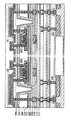
図1(A)、図1(B)、図1(C)、図1(D)、および図1(E)は、半導体装置1000を示す上面図および断面図である。半導体装置1000はトランジスタ200およびトランジスタ400を有する。基板(図示せず)の上に形成されたトランジスタ200およびトランジスタ400は、異なる構成を有する。例えば、トランジスタ400は、トランジスタ200と比較して、バックゲート電圧及びトップゲート電圧が0Vのときのドレイン電流(以下、Icutと呼ぶ。)が小さい構成とすればよい。トランジスタ400をスイッチング素子として、トランジスタ200のバックゲートの電位を制御できる構成とする。これにより、トランジスタ200のバックゲートと接続するノードを所望の電位にした後、トランジスタ400をオフ状態にすることで、トランジスタ200のバックゲートと接続するノードの電荷が消失することを抑制することができる。<Configuration Example of
1A, 1B, 1C, 1D, and 1E are a top view and a cross-sectional view illustrating a
ここで、図1(A)は半導体装置1000の上面図である。図1(B)は、図1(A)中の一点鎖線L1−L2に対応しており、トランジスタ200およびトランジスタ400のチャネル長方向の断面図である。また、図1(C)は、図1(A)中の一点鎖線W1−W2に対応しており、トランジスタ200のチャネル幅方向の断面図である。また、図1(D)は、図1(A)中の一点鎖線W3−W4に対応するトランジスタ200の断面図である。また、図1(E)は、図1(A)中の一点鎖線W5−W6に対応しており、トランジスタ400のチャネル幅方向の断面図である。Here, FIG. 1A is a top view of the
以下、トランジスタ200とトランジスタ400の構成についてそれぞれ図1(A)、図1(B)、図1(C)、図1(D)、および図1(E)を用いて説明する。なお、トランジスタ200とトランジスタ400の構成材料の詳細については<構成材料について>で詳細に説明する。Hereinafter, structures of the
〔トランジスタ200〕
図1(A)、図1(B)、図1(C)、および図1(D)に示すように、トランジスタ200は、絶縁体210の上に配置された絶縁体212と、絶縁体212の上に配置された絶縁体214と、絶縁体214の上に配置された導電体205(導電体205a、および導電体205b)と、導電体205の上に配置された絶縁体220、絶縁体222、および絶縁体224と、絶縁体224の上に配置された酸化物230(酸化物230a、酸化物230b、および酸化物230c)と、酸化物230bの上に配置された導電体240a、および導電体240b(以下、導電体240a、および導電体240bをまとめて導電体240ともいう)と、導電体240の上に配置された層245a、および層245b(以下、層245a、および層245bをまとめて層245ともいう)と、酸化物230cの上に配置された絶縁体250と、絶縁体250の上に配置された導電体260(導電体260a、導電体260b、および導電体260c)と、導電体260cの上に配置された層270と、層270の上に配置された絶縁体272と、絶縁体272の上に配置された絶縁体274と、を有する。[Transistor 200]
As shown in FIGS. 1A, 1B, 1C, and 1D, the
絶縁体212及び絶縁体214は、水または水素などの不純物が透過しにくい絶縁性材料を用いることが好ましく、例えば、酸化アルミニウムなどを用いることが好ましい。これにより、絶縁体210より下層から水素、水などの不純物が絶縁体212及び絶縁体214より上層に拡散するのを抑制することができる。なお、絶縁体212及び絶縁体214は、水素原子、水素分子、水分子、酸素原子、酸素分子、窒素原子、窒素分子、酸化窒素分子(N2O、NO、NO2など)、銅原子などの不純物の少なくとも一が透過しにくいことが好ましい。また、以下において、不純物が透過しにくい絶縁性材料について記載する場合も同様である。The
また、例えば、絶縁体212は原子層堆積(ALD:Atomic Layer Deposition)法を用いて成膜することが好ましい。これにより、絶縁体212を良好な被覆性で成膜し、クラックやピンホールなどが形成されることを抑制することができる。また、例えば、絶縁体214をスパッタリング法を用いて成膜することが好ましい。これにより、絶縁体212より速い成膜速度で成膜でき、絶縁体212より生産性よく膜厚を大きくすることができる。このような絶縁体212と絶縁体214の積層にすることで、水素、水などの不純物に対するバリア性を向上させることができる。なお、絶縁体212は、絶縁体214の下に設ける構成としてもよい。また、絶縁体214が不純物に対して十分なバリア性を持つ場合、絶縁体212を設けない構成としてもよい。For example, the
また、絶縁体212及び絶縁体214は、酸素が透過しにくい絶縁性材料を用いることが好ましい。これにより、絶縁体224などに含まれる酸素が下方拡散するのを抑制することができる。これにより、酸化物230bに効果的に酸素を供給することができる。The
ここで、絶縁体210、絶縁体212、および絶縁体214は開口が形成されており、当該開口の内側は、絶縁体210、絶縁体212、および絶縁体214が同一面上となる。絶縁体216に複数の開口が形成されており、その一つは、絶縁体210、絶縁体212、および絶縁体214の開口の位置に重なるように形成され、当該開口の径は、絶縁体210、絶縁体212、および絶縁体214の開口より大きい。また、絶縁体216の他の開口は絶縁体214の上面に達する。Here, an opening is formed in the
絶縁体216の開口の内側に接して導電体205aが形成され、さらに内側に導電体205bが形成されている。ここで、導電体205aおよび導電体205bの上面の高さと、絶縁体216の上面の高さは同程度にできる。A
また、導電体205と同様に、導電体207を設けてもよい。導電体207は、絶縁体210、絶縁体212、絶縁体214、および絶縁体216に形成された開口の中に設けられている。導電体207の絶縁体216と同じ層に形成される部分が配線として機能し、導電体207の絶縁体210、絶縁体212、および絶縁体216と同じ層に形成される部分がプラグとして機能する。導電体207は、上記開口の内側に接して導電体207aが形成され、導電体207aを介して開口の内側に導電体207bが形成される。ここで、導電体207aおよび導電体207bの上面の高さと、絶縁体216の上面の高さは同程度にできる。このような導電体207を設けることで、絶縁体210より下層に位置する配線、回路素子、半導体素子などと接続することができる。また、導電体207より上層に同様の配線とプラグを設けることにより、上層に位置する配線、回路素子、半導体素子などと接続することができる。Further, like the
ここで、導電体205a及び導電体207aは、水または水素などの不純物が透過しにくい導電性材料を用いることが好ましい。また、例えば、タンタル、窒化タンタル、ルテニウムまたは酸化ルテニウムなどを用いることが好ましく、単層または積層とすればよい。これにより、絶縁体210より下層から水素、水などの不純物が導電体205または導電体207を通じて上層に拡散するのを抑制することができる。なお、導電体205a及び導電体207aは、水素原子、水素分子、水分子、酸素原子、酸素分子、窒素原子、窒素分子、酸化窒素分子(N2O、NO、NO2など)、銅原子などの不純物の少なくとも一が透過しにくいことが好ましい。また、以下において、不純物が透過しにくい導電性材料について記載する場合も同様である。Here, it is preferable that the
また、導電体205b及び導電体207bに、銅など酸化シリコン中を拡散しやすい金属を用いる場合、絶縁体220として、窒化シリコン、窒化酸化シリコンなどの銅が透過しにくい絶縁性材料を用いることにより、銅などの不純物が絶縁体220より上に拡散することを防ぐことができる。このとき、導電体205a、導電体207aも銅が透過しにくい絶縁性材料を用いて、銅などの不純物が導電体205a、導電体205bの外に銅などの不純物が拡散しないようにすることが好ましい。In the case where a metal that easily diffuses in silicon oxide such as copper is used for the
また、絶縁体222は、水または水素などの不純物、および酸素が透過しにくい絶縁性材料を用いることが好ましく、例えば、酸化アルミニウム、および酸化ハフニウムなどを用いることが好ましい。これにより、絶縁体210より下層から水素、水などの不純物が絶縁体212及び絶縁体214より上層に拡散するのを抑制することができる。さらに、絶縁体224などに含まれる酸素が下方拡散するのを抑制することができる。The
絶縁体224は、加熱により酸素が放出される絶縁体を用いて形成することが好ましい。具体的には、昇温脱離ガス分析法(TDS(Thermal Desorption Spectroscopy))にて、酸素原子に換算した酸素の脱離量が1.0×10¹⁸atoms/cm3以上、好ましくは3.0×1020atoms/cm3以上である絶縁体を用いることが好ましい。なお、加熱により放出される酸素を「過剰酸素」ともいう。このような絶縁体224を酸化物230に接して設けることにより、酸化物230bに効果的に酸素を供給することができる。The
また、絶縁体224中の水、水素または窒素酸化物などの不純物濃度が低減されていることが好ましい。例えば、絶縁体224の水素の脱離量は、TDSにおいて、50℃から500℃の範囲において、水素分子に換算した脱離量が、絶縁体224の面積当たりに換算して、2×10¹⁵molecules/cm2以下、好ましくは1×1015molecules/cm2以下、より好ましくは5×1014molecules/cm2以下であればよい。In addition, the concentration of impurities such as water, hydrogen, or nitrogen oxide in the
酸化物230aは、例えば、酸素雰囲気下で成膜した酸化物を用いることが好ましい。これにより、酸化物230aの形状の安定を図ることができる。なお、酸化物230a乃至酸化物230cの構成の詳細については後述する。As the
トランジスタ200に安定した電気特性及び、良好な信頼性を付与するには、酸化物230bが、酸化物中の不純物及び酸素欠損が低減され、高純度真性または実質的に高純度真性であることが好ましい。高純度真性または実質的に高純度真性である酸化物は、欠陥準位密度が低いため、トラップ準位密度も低くなる場合がある。In order to impart stable electric characteristics and good reliability to the
また、酸化物のトラップ準位に捕獲された電荷は、消失するまでに要する時間が長く、あたかも固定電荷のように振る舞うことがある。そのため、トラップ準位密度の高い酸化物にチャネル領域が形成されるトランジスタは、電気特性が不安定となり、信頼性が低下する場合がある。In addition, the charge trapped in the trap level of the oxide takes a long time to disappear, and may behave as if it were a fixed charge. Therefore, a transistor in which a channel region is formed in an oxide having a high trap state density may have unstable electrical characteristics and may decrease reliability.
従って、トランジスタの電気特性を安定させ、信頼性を向上させるためには、酸化物中の酸素欠損及び不純物濃度を低減することが有効である。また、酸化物中の不純物濃度を低減するためには、近接する膜中の不純物濃度も低減することが好ましい。Therefore, in order to stabilize the electrical characteristics of the transistor and improve the reliability, it is effective to reduce oxygen vacancies and impurity concentrations in the oxide. In order to reduce the impurity concentration in the oxide, it is preferable to reduce the impurity concentration in the adjacent film.
また、酸化物230bは、酸化物230aおよび酸化物230cよりも電子親和力の大きい酸化物を用いる。例えば、酸化物230bとして、酸化物230aおよび酸化物230cよりも電子親和力が0.07eV以上1.3eV以下、好ましくは0.1eV以上0.7eV以下、さらに好ましくは0.1eV以上0.4eV以下大きい酸化物を用いる。なお、電子親和力は、真空準位と伝導帯下端のエネルギーとの差である。As the
また、酸化物230bは、第1の領域、第2の領域、および第3の領域を有する。第3の領域は、上面図において第1の領域と第2の領域に挟まれる。トランジスタ200は、酸化物230bの第1の領域上に導電体240aを有し、酸化物230bの第2の領域上に導電体240bを有する。導電体240aまたは導電体240bの一方は、ソース導電体またはドレイン導電体の一方として機能でき、他方は、ソース導電体またはドレイン導電体の他方として機能できる。よって、酸化物230bの第1の領域または第2の領域の一方は、ソース領域として機能でき、他方はドレイン領域として機能できる。また、酸化物230bの第3の領域はチャネル形成領域として機能できる。In addition, the
ここで、導電体240a及び導電体240bの酸化物230cと接する側の側面が、90度よりも小さいテーパー角を有することが好ましい。導電体240または導電体240bの酸化物230cと接する側の側面と底面のなす角が45°以上75°以下であることが好ましい。このように導電体240a及び導電体240bを形成することにより、酸化物230cを導電体240が形成する段差部にも被覆性良く成膜することができる。これにより、酸化物230cが段切れなどを起こして、酸化物230bと絶縁体250などが接するのを防ぐことができる。Here, the side surfaces of the
また、導電体240a上に層245aが形成され、導電体240b上に層245bが形成される。ここで、層245aおよび層245bは、酸素が透過しにくい材料を用いることが好ましく、例えば酸化アルミニウムなどを用いることができる。これにより、導電体240a及び導電体240bの酸化によって周囲の過剰酸素が消費されることを防ぐことができる。Further, the
酸化物230cは、層245a、層245b、導電体240a、導電体240b、酸化物230b、および酸化物230a上に形成される。ここで、酸化物230cは、酸化物230bの上面と、酸化物230bのチャネル幅方向の側面と、酸化物230aのチャネル幅方向の側面と、絶縁体224の上面と接する。酸化物230cは、酸化物230bに酸素を供給する機能を有する場合がある。また、酸化物230cの上に絶縁体250を形成することにより、絶縁体250から水または水素などの不純物が酸化物230bに直接浸入することを防ぐことができる。また、例えば、酸素雰囲気下で成膜した酸化物を用いることが好ましい。これにより、酸化物230cの形状の安定を図ることができる。The
絶縁体250はゲート絶縁膜として機能できる。絶縁体250は、絶縁体224と同様に、加熱により酸素が放出される絶縁体を用いて形成することが好ましい。このような絶縁体250を酸化物230に接して設けることにより、酸化物230に効果的に酸素を供給することができる。また、絶縁体224と同様に、絶縁体250中の水または水素などの不純物濃度が低減されていることが好ましい。The
絶縁体250上に導電体260aを有し、導電体260a上に導電体260bを有し、導電体260b上に導電体260cを有する。絶縁体250および導電体260は、第3の領域と重なる領域を有する。また、絶縁体250、導電体260a、導電体260bおよび導電体260cの端部は概略一致する。A
なお、導電体205または導電体260の一方はゲート電極として機能でき、他方はバックゲート電極として機能できる。ゲート電極とバックゲート電極で半導体のチャネル形成領域を挟むように配置される。バックゲート電極の電位は、ゲート電極と同電位としてもよいし、接地電位や、任意の電位としてもよい。また、バックゲート電極の電位をゲート電極と連動させず独立して変化させることで、トランジスタのしきい値電圧を変化させることができる。Note that one of the
導電体260aは、酸化物で導電性を有するものが好ましい。例えば、酸化物230として用いることができるIn−Ga−Zn系酸化物のうち、導電性が高い、金属の原子数比が[In]:[Ga]:[Zn]=4:2:3から4.1、およびその近傍値ものを用いることが好ましい。The
導電体260bは、導電体260aに窒素などの不純物を添加して導電体260aの導電性を向上できる導電体が好ましい。例えば導電体260aにIn−Ga−Zn系酸化物を用いる場合、導電体260bは窒化チタンなどを用いることが好ましい。また、例えば導電体260cには、導電性が低いタングステンを用いることが好ましい。The conductor 260b is preferably a conductor that can improve the conductivity of the
また、導電体260上に層270が形成されている。ここで、層270は、酸素が透過しにくい材料を用いることが好ましく、例えば酸化アルミニウムなどを用いることができる。これにより、導電体260の酸化によって周囲の過剰酸素が消費されることを防ぐことができる。このように、層270はゲートを保護するゲートキャップとしての機能を有する。層270および酸化物230cは、導電体260の端部を越えて延伸し、当該延伸部分で重畳して接する領域を有し、層270の端部と酸化物230cの端部は概略一致している。A
絶縁体272は、酸化物230、導電体240、層245、絶縁体250、導電体260、および層270を覆って設けられている。さらに絶縁体272は、酸化物230bの側面及び絶縁体224の上面と接して設けられている。さらに、絶縁体272の上に絶縁体274が設けられている。The
ここで、絶縁体272は、スパッタリング法を用いて成膜された酸化物絶縁体を用いることが好ましく、例えば酸化アルミニウムを用いることが好ましい。このような絶縁体272を用いることにより、絶縁体224及び酸化物230bの絶縁体272と接する面に酸素を添加して、酸素過剰な状態にできる。Here, as the
また、絶縁体272は、加熱処理を行うことにより、酸化物230および絶縁体224中の水素をゲッタリングする性質をもつことが好ましく、例えば、酸化アルミニウムを用いることが好ましい。これにより、絶縁体224及び酸化物230b中の水または水素などの不純物を低減させることができる。The
また、絶縁体272及び絶縁体274は、水または水素などの不純物が透過しにくい絶縁性材料を用いることが好ましく、例えば、酸化アルミニウムなどを用いることが好ましい。このような絶縁体272を用いることにより、絶縁体274より上層から水素、水などの不純物が絶縁体272より下層に拡散するのを抑制することができる。The
さらに、絶縁体274はALD法を用いて成膜された酸化物絶縁体を用いることが好ましく、例えば酸化アルミニウムを用いることが好ましい。ALD法を用いて成膜された絶縁体274は、良好な被覆性を有し、クラックやピンホールなどの形成が抑制された膜となる。絶縁体272及び絶縁体274は凹凸を有する形状の上に設けられるが、ALD法で成膜された絶縁体274を用いることにより、段切れ、クラック、ピンホールなどが形成されることなく、トランジスタ200を絶縁体274で覆うことができる。これにより、絶縁体272に段切れなどが発生しても、絶縁体274で覆うことができるので、絶縁体272と絶縁体274の積層膜の、水素、水などの不純物に対するバリア性をより顕著に向上させることができる。Further, the
また、絶縁体272をスパッタリング法で成膜し、絶縁体274をALD法で成膜した場合、導電体260cの導電体240と重畳する領域の上面が被形成面となる部分の膜厚(以下、第1の膜厚とよぶ。)と、酸化物230a、酸化物230b、および導電体240の側面が被形成面となる部分の膜厚(以下、第2の膜厚とよぶ。)と、で絶縁体272及び絶縁体274で膜厚の比が異なる場合がある。絶縁体272では、第1の膜厚と、第2の膜厚とを同程度の大きさとすることができる。これに対して、絶縁体274では、第1の膜厚が第2の膜厚より大きくなる場合が多く、例えば、第1の膜厚が第2の膜厚の2倍程度になる場合がある。Further, in the case where the
また、絶縁体272及び絶縁体274は、酸素が透過しにくい絶縁性材料を用いることが好ましい。これにより、絶縁体224、絶縁体250などに含まれる酸素が上方拡散するのを抑制することができる。The
このように、トランジスタ200は、絶縁体274、絶縁体272、絶縁体214、および絶縁体212に挟まれる構造とすることによって、酸素を外方拡散させず、絶縁体224、酸化物230、および絶縁体250中に多くの酸素を含有させることができる。さらに、絶縁体274の上方および絶縁体212の下方から水素、または水などの不純物が混入するのを防ぎ、絶縁体224、酸化物230、および絶縁体250中の不純物濃度を低減させることができる。In this manner, the
このようにして、トランジスタ200の活性層として機能する酸化物230b中の酸素欠損を低減し、水素または水などの不純物を低減することで、トランジスタ200の電気特性を安定させ、信頼性を向上させることができる。In this manner, oxygen vacancies in the
絶縁体274の上には、絶縁体280が設けられている。絶縁体280は、絶縁体224などと同様に、膜中の水または水素などの不純物濃度が低減されていることが好ましい。An
さらに、絶縁体280の上に絶縁体282が設けられ、絶縁体282の上に絶縁体284が設けられている。絶縁体282及び絶縁体284は、絶縁体272及び絶縁体274と同様に、水、水素などの不純物、および酸素が透過しにくい絶縁性材料、例えば酸化アルミニウムを用いることが好ましい。Further, an
絶縁体282は、絶縁体272と同様に、加熱処理を行うことにより、絶縁体280中の水素をゲッタリングする性質をもつことが好ましく、例えば、酸化アルミニウムを用いることが好ましい。このような絶縁体282を設けることで、絶縁体280の膜中の水または水素などの不純物濃度を低減することができる。Like the
また、絶縁体284は、絶縁体274と同様に、ALD法を用いて成膜された酸化物絶縁体を用いることが好ましく、例えば酸化アルミニウムを用いることが好ましい。このような絶縁体274を用いることにより、絶縁体284より上層から水素、水などの不純物が絶縁体282より下層に拡散するのを抑制することができる。As the
ここで、絶縁体216、絶縁体220、絶縁体222、絶縁体224、絶縁体272、絶縁体274及び絶縁体280には、絶縁体214に達する開口480が形成されている。絶縁体282は、開口480の内側にも成膜されており、絶縁体214の上面と接している。なお、図1(A)では、W1−W2方向に伸長された開口480の一部だけが示されているが、開口480はトランジスタ200及びトランジスタ400を囲むように形成され、少なくとも酸化物230より外側を囲むように開口480が形成される。また、開口480は閉じており、開口480より内側の領域と開口480より外側の領域を分断していることが好ましい。開口480において、絶縁体214の上面と絶縁体282の下面が接しており、開口480で囲まれる領域は、絶縁体214と絶縁体282で囲まれる領域ということができる。Here, an
このような構造とすることにより、トランジスタ200を基板の上下方向だけでなく、側面方向からも絶縁体282及び絶縁体284で囲んで封止することができる。これにより、絶縁体284の外側から水、または水素などの不純物がトランジスタ200及びトランジスタ400に拡散するのを防ぐことができる。さらに、絶縁体282をALD法で成膜することにより、開口480においても段切れなどを起こさずに、成膜できる。これにより、絶縁体282に段切れなどが発生しても、絶縁体284で覆うことができるので、絶縁体282と絶縁体284の積層膜の、不純物に対するバリア性を向上させることができる。With such a structure, the
また、開口480は、半導体装置1000を切り出すダイシングラインまたはスクライブラインの内側に位置するように設けることが好ましい。これにより、半導体装置1000を切り出した時も、絶縁体280、絶縁体224、絶縁体216などの側面が絶縁体282及び絶縁体284で封止されたままなので、これらの絶縁体から、水素または水などの不純物が浸入してトランジスタ200及びトランジスタ400に拡散するのを防ぐことができる。なお、ダイシングラインまたはスクライブラインの内側に開口480で囲まれる領域を複数設け、複数の半導体装置を個別に、絶縁体282及び絶縁体284で封止する構造としてもよい。The
〔トランジスタ400〕
図1(A)、図1(B)、図1(E)に示すように、トランジスタ400は、絶縁体210の上に配置された絶縁体212と、絶縁体212の上に配置された絶縁体214と、絶縁体214の上に配置された導電体403(導電体403a、および導電体403b)、導電体405(導電体405a、および導電体405b)、導電体407(導電体407a、および導電体407b)と、導電体403、導電体405、および導電体407の上に配置された絶縁体220、絶縁体222、および絶縁体224と、絶縁体224、導電体405、および導電体407の上に配置された酸化物430と、酸化物430の上に配置された絶縁体450と、絶縁体450の上に配置された導電体460(導電体460a、導電体460b、および導電体460c)と、導電体460cの上に配置された層470と、層470の上に配置された絶縁体272と、絶縁体272の上に配置された絶縁体274と、を有する。以下、トランジスタ200で説明した構成については省略する。[Transistor 400]
As shown in FIGS. 1A, 1B, and 1E, the
絶縁体216の開口に導電体403、導電体405、および導電体407が設けられる。導電体403、導電体405、および導電体407は導電体205と同様の構成にすることが好ましい。絶縁体216の開口の内側に接して導電体403aが形成され、さらに内側に導電体403bが形成されている。導電体405及び導電体407も、導電体403と同様の構成である。導電体405または導電体407の一方は、ソース導電体またはドレイン導電体の一方として機能でき、他方は、ソース導電体またはドレイン導電体の他方として機能できる。A
酸化物430は、酸化物230cと同様の構成とすることが好ましい。また、酸化物430は、第1の領域、第2の領域、および第3の領域を有する。第3の領域は、上面図において第1の領域と第2の領域に挟まれる。トランジスタ400は、酸化物430の第1の領域の下に導電体405を有し、酸化物430の第2の領域の下に導電体407を有する。よって、酸化物430の第1の領域または第2の領域の一方は、ソース領域として機能でき、他方はドレイン領域として機能できる。また、酸化物430の第3の領域はチャネル形成領域として機能できる。The
なお、トランジスタ200では、酸化物230bにチャネルが形成されるが、トランジスタ400では酸化物430にチャネルが形成される。酸化物230bと酸化物430は、電気的性質の異なる半導体材料を用いることが好ましい。酸化物230bと酸化物430に電気的性質の異なる半導体材料を用いることで、トランジスタ200とトランジスタ400の電気特性を異ならせることができる。Note that a channel is formed in the
また、例えば、酸化物430に、酸化物230bよりも電子親和力が小さい半導体を用いることで、トランジスタ400のしきい値電圧をトランジスタ200よりも大きくすることができる。具体的には、酸化物430及び酸化物230bがIn−M−Zn酸化物(Inと元素MとZnを含む酸化物)であるとき、酸化物430をIn:M:Zn=x1:y 1:z1[原子数比]、酸化物230bをIn:M:Zn=x2:y2:z2[原子数比]とすると、y1/x1がy2/x2よりも大きくなる酸化物430、および酸化物230bを用いればよい。酸化物230bは、例えば、ターゲットの原子数比が、In:M:Zn=1:1:1、In:M:Zn=1:1:1.2、In:M:Zn=2:1:1.5、In:M:Zn=2:1:2.3、In:M:Zn=2:1:3、In:M:Zn=3:1:2、In:M:Zn=4:2:4.1、In:M:Zn=4:2:3、In:M:Zn=5:1:7等を用いて成膜したものが好ましい。また、酸化物430は、例えば、ターゲットの原子数比が、In:M:Zn=1:2:4、In:M:Zn=1:3:2、In:M:Zn=1:3:4、In:M:Zn=1:3:6、In:M:Zn=1:3:8、In:M:Zn=1:4:3、In:M:Zn=1:4:4、In:M:Zn=1:4:5、In:M:Zn=1:4:6、In:M:Zn=1:6:3、In:M:Zn=1:6:4、In:M:Zn=1:6:5、In:M:Zn=1:6:6、In:M:Zn=1:6:7、In:M:Zn=1:6:8、In:M:Zn=1:6:9、In:M:Zn=1:10:1等を用いて成膜したものが好ましい。ただし、これに限られることなく、上記の式を満たす範囲で酸化物430および酸化物230bの原子数比を適宜設定すればよい。このようなIn−M−Zn酸化物を用いることで、トランジスタ400のVthをトランジスタ200よりも大きくすることができる。For example, the threshold voltage of the
また、トランジスタ400では酸化物230のチャネルが形成される領域が絶縁体224と絶縁体450に直接接しているため、界面散乱やトラップ準位の影響を受けやすい。これにより、トランジスタ400の電界効果移動度及びキャリア密度を小さくすることができる。また、トランジスタ400のしきい値電圧をトランジスタ200よりも大きくすることができる。Further, in the
酸化物430は、過剰酸素を多く含むことが好ましく、例えば、酸素雰囲気下で成膜した酸化物を用いることが好ましい。このような酸化物430を活性層として用いることにより、トランジスタ400のしきい値電圧を0Vより大きくし、オフ電流を低減し、Icutを非常に小さくすることができる。The
絶縁体450は、絶縁体250と同様の構成とすることが好ましく、ゲート絶縁膜として機能できる。このような絶縁体450を酸化物430に接して設けることにより、酸化物430に効果的に酸素を供給することができる。また、絶縁体224と同様に、絶縁体450中の水または水素などの不純物濃度が低減されていることが好ましい。The
導電体460は、導電体260と同様の構成とすることが好ましい。絶縁体450上に導電体460aを有し、導電体460a上に導電体460bを有し、導電体460b上に導電体460cを有する。絶縁体450および導電体460は、第3の領域と重なる領域を有する。また、絶縁体450、導電体460a、導電体460bおよび導電体460cの端部は概略一致する。なお、導電体403または導電体460の一方はゲート電極として機能でき、他方はバックゲート電極として機能できる。The
層470は、層270と同様の構成とすることが好ましい。導電体460上に層470が形成されている。これにより、導電体460の酸化によって周囲の過剰酸素が消費されることを防ぐことができる。層470および酸化物430は、導電体460の端部を越えて延伸し、当該延伸部分で重畳し、接する領域を有し、層470の端部と酸化物430の端部は概略一致している。The
トランジスタ400も、トランジスタ200と同様に、絶縁体274、絶縁体272、絶縁体214、および絶縁体212に挟まれる構造とすることによって、酸素を外方拡散させず、絶縁体224、酸化物430、および絶縁体450中に多くの酸素を含有させることができる。さらに、絶縁体274の上方および絶縁体212の下方から水素、または水などの不純物が混入するのを防ぎ、絶縁体224、酸化物230、および絶縁体250中の不純物濃度を低減させることができる。Similarly to the
このようにして、トランジスタ400の活性層として機能する酸化物430中の酸素欠損を低減し、水素または水などの不純物を低減することで、トランジスタ400のしきい値電圧を0Vより大きくし、オフ電流を低減し、Icutを非常に小さくすることができる。さらに、トランジスタ400の電気特性を安定させ、信頼性を向上させることができる。In this manner, oxygen vacancies in the
このようなトランジスタ400をスイッチング素子としてトランジスタ200のバックゲートの電位を保持できる構成とすることにより、トランジスタ200のオフ状態を長く維持することができる。By using the
<構成材料について>
〔絶縁体〕
絶縁体210、絶縁体216、絶縁体220、絶縁体224、絶縁体250、絶縁体450、および絶縁体280は、例えば、ホウ素、炭素、窒素、酸素、フッ素、マグネシウム、アルミニウム、シリコン、リン、アルゴン、ガリウム、ゲルマニウム、イットリウム、ジルコニウム、ランタン、ネオジム、ハフニウムまたはタンタルを含む絶縁材料を、単層で、または積層で用いればよい。例えば、酸化シリコン、酸化窒化シリコン、窒化酸化シリコン、窒化シリコン、窒化アルミニウム、酸化アルミニウム、窒化酸化アルミニウム、酸化窒化アルミニウム、酸化マグネシウム、酸化ガリウム、酸化ゲルマニウム、酸化イットリウム、酸化ジルコニウム、酸化ランタン、酸化ネオジム、酸化ハフニウム、酸化タンタル、アルミニウムシリケートなどから選ばれた材料を、単層でまたは積層して用いる。また、酸化物材料、窒化物材料、酸化窒化物材料、窒化酸化物材料のうち、複数の材料を混合した材料を用いてもよい。<Constituent materials>
〔Insulator〕
The
なお、本明細書中において、窒化酸化物とは、酸素よりも窒素の含有量が多い化合物をいう。また、酸化窒化物とは、窒素よりも酸素の含有量が多い化合物をいう。なお、各元素の含有量は、例えば、ラザフォード後方散乱法(RBS:Rutherford Backscattering Spectrometry)等を用いて測定することができる。Note that in this specification, a nitrided oxide refers to a compound having a higher nitrogen content than oxygen. Further, oxynitride refers to a compound having a higher oxygen content than nitrogen. The content of each element can be measured using, for example, Rutherford Backscattering Spectrometry (RBS).
絶縁体212、絶縁体214、絶縁体222、絶縁体272、絶縁体274、絶縁体282、および絶縁体284は、絶縁体224、絶縁体250、絶縁体450、および絶縁体280より、水または水素などの不純物が透過しにくい絶縁性材料を用いて形成することが好ましい。例えば、不純物が透過しにくい絶縁性材料として、酸化アルミニウム、窒化アルミニウム、酸化窒化アルミニウム、窒化酸化アルミニウム、酸化ガリウム、酸化ゲルマニウム、酸化イットリウム、酸化ジルコニウム、酸化ランタン、酸化ネオジム、酸化ハフニウム、酸化タンタル、窒化シリコンなどを挙げることができる。これらを単層で、または積層で用いればよい。The
絶縁体212、絶縁体214、および絶縁体222に不純物が透過しにくい絶縁性材料を用いることで、基板側からトランジスタへの不純物の拡散を抑制し、トランジスタの信頼性を高めることができる。絶縁体272、絶縁体274、絶縁体282、および絶縁体284に不純物が透過しにくい絶縁性材料を用いることで、絶縁体280よりも上層からトランジスタへの不純物の拡散を抑制し、トランジスタの信頼性を高めることができる。By using an insulating material that does not easily transmit impurities for the
なお、絶縁体212、絶縁体214、絶縁体272、絶縁体282、および絶縁体284として、これらの材料で形成される絶縁層を複数積層して用いてもよい。また、絶縁体212、絶縁体214のどちらか一方を省略してもよい。また、絶縁体282、絶縁体284のどちらか一方を省略してもよい。Note that as the
ここで、不純物が透過しにくい絶縁性材料とは、耐酸化性が高く、酸素、水素または水に代表される不純物の拡散を抑制する機能とする。Here, the insulating material which does not easily transmit impurities has high oxidation resistance and a function of suppressing diffusion of impurities typified by oxygen, hydrogen, or water.
例えば、酸化シリコンに対し、酸化アルミニウムは、350℃または400℃の雰囲気下において、不純物が透過しにくい絶縁性材料中の一時間当たりの酸素または水素の拡散距離が非常に小さい。従って、酸化アルミニウムは不純物が透過しにくい材料であるといえる。For example, in contrast to silicon oxide, aluminum oxide has a very small diffusion distance of oxygen or hydrogen per hour in an insulating material that hardly permeates impurities in an atmosphere at 350 ° C. or 400 ° C. Therefore, it can be said that aluminum oxide is a material that hardly permeates impurities.
また、不純物が透過しにくい絶縁性材料の一例として、例えば、CVD法で形成した窒化シリコンを用いることができる。ここで、トランジスタ200等の酸化物半導体を有する半導体素子に、水素が拡散することで、該半導体素子の特性が低下する場合がある。従って、トランジスタ200は、水素の拡散を抑制する膜で封止されていることが好ましい。水素の拡散を抑制する膜とは、具体的には、水素の脱離量が少ない膜とする。For example, silicon nitride formed by a CVD method can be used as an example of an insulating material that does not easily transmit impurities. Here, when hydrogen diffuses into a semiconductor element including an oxide semiconductor such as the
水素の脱離量は、例えば、TDSなどを用いて分析することができる。例えば、絶縁体212の水素の脱離量は、TDSにおいて、50℃から500℃の範囲において、水素分子に換算した脱離量が、絶縁体212の面積当たりに換算して、2×10¹⁵molecules/cm2以下、好ましくは1×1015molecules/cm2以下、より好ましくは5×1014molecules/cm2以下であればよい。The amount of hydrogen desorption can be analyzed using, for example, TDS. For example, the amount of hydrogen desorbed from the
また、特に、絶縁体216、絶縁体224、および絶縁体280は、誘電率が低いことが好ましい。例えば、絶縁体216、絶縁体224、および絶縁体280の比誘電率は、3未満、好ましくは2.4未満、さらに好ましくは1.8未満であることが好ましい。誘電率が低い材料を層間膜とすることで、配線間に生じる寄生容量を低減することができる。不純物が透過しにくい絶縁性材料を用いて形成することが好ましい。In particular, the
また、酸化物230として酸化物半導体を用いる場合は、酸化物230中の水素濃度の増加を防ぐために、絶縁体中の水素濃度を低減することが好ましい。具体的には、絶縁体中の水素濃度を、SIMSにおいて2×10²⁰atoms/cm3以下、好ましくは5×1019atoms/cm3以下、より好ましくは1×1019atoms/cm3以下、さらに好ましくは5×1018atoms/cm3以下とする。特に、絶縁体216、絶縁体224、絶縁体250、絶縁体450、および絶縁体280の水素濃度を低減することが好ましい。少なくとも、酸化物230、または酸化物430と接する絶縁体224、絶縁体250、および絶縁体450の水素濃度を低減することが好ましい。In the case where an oxide semiconductor is used as the
また、酸化物230中の窒素濃度の増加を防ぐために、絶縁体中の窒素濃度を低減することが好ましい。具体的には、絶縁体中の窒素濃度を、SIMSにおいて5×10¹⁹atoms/cm3以下、好ましくは5×1018atoms/cm3以下、より好ましくは1×1018atoms/cm3以下、さらに好ましくは5×1017atoms/cm 3以下とする。In order to prevent an increase in the nitrogen concentration in the
また、絶縁体224の少なくとも酸化物230と接する領域と、絶縁体250の少なくとも酸化物230と接する領域は、欠陥が少ないことが好ましく、代表的には、電子スピン共鳴法(ESR:Electron Spin Resonance)で観察されるシグナルが少ない方が好ましい。例えば、上述のシグナルとしては、g値が2.001に観察されるE’センターが挙げられる。なお、E’センターは、シリコンのダングリングボンドに起因する。絶縁体224および絶縁体250として酸化シリコン層または酸化窒化シリコン層を用いる場合は、E’センター起因のスピン密度が、3×10¹⁷spins/cm3以下、好ましくは5×1016spins/cm3以下である酸化シリコン層、または酸化窒化シリコン層を用いればよい。It is preferable that at least a region of the
また、上述のシグナル以外に二酸化窒素(NO2)に起因するシグナルが観察される場合がある。当該シグナルは、Nの核スピンにより3つのシグナルに分裂しており、それぞれのg値が2.037以上2.039以下(第1のシグナルとする)、g値が2.001以上2.003以下(第2のシグナルとする)、及びg値が1.964以上1.966以下(第3のシグナルとする)に観察される。In addition to the above signal, a signal due to nitrogen dioxide (NO 2 ) may be observed. The signal is split into three signals by N nuclear spins, each having a g value of 2.037 or more and 2.039 or less (referred to as the first signal), and a g value of 2.001 or more and 2.003. The g value is observed below (referred to as the second signal) and from 1.964 to 1.966 (referred to as the third signal).
例えば、絶縁体224および絶縁体250として、二酸化窒素(NO2)起因のスピン密度が、1×10¹⁷spins/cm3以上1×1018spins/cm3未満である絶縁層を用いると好適である。For example, as the
なお、二酸化窒素(NO2)を含む窒素酸化物(NOx)は、絶縁層中に準位を形成する。当該準位は、酸化物半導体のエネルギーギャップ内に位置する。そのため、窒素酸化物(NOx)が、絶縁層と酸化物半導体の界面に拡散すると、当該準位が絶縁層側において電子をトラップする場合がある。この結果、トラップされた電子が、絶縁層と酸化物半導体の界面近傍に留まるため、トランジスタのしきい値電圧をプラス方向にシフトさせてしまう。したがって、絶縁体224および絶縁体250として窒素酸化物の含有量が少ない膜を用いると、トランジスタのしきい値電圧のシフトを低減することができる。Note that nitrogen oxide (NO x ) containing nitrogen dioxide (NO 2 ) forms a level in the insulating layer. The level is located in the energy gap of the oxide semiconductor. Therefore, when nitrogen oxide (NOx) diffuses to the interface between the insulating layer and the oxide semiconductor, the level may trap electrons on the insulating layer side. As a result, trapped electrons remain in the vicinity of the interface between the insulating layer and the oxide semiconductor, so that the threshold voltage of the transistor is shifted in the positive direction. Therefore, when a film with a low content of nitrogen oxide is used as the
窒素酸化物(NOx)の放出量が少ない絶縁層としては、例えば、酸化窒化シリコン層を用いることができる。当該酸化窒化シリコン層は、TDSにおいて、窒素酸化物(NOx)の放出量よりアンモニアの放出量が多い膜であり、代表的にはアンモニアの放出量が1×10¹⁸個/cm3以上5×1019個/cm3以下である。なお、上記のアンモニアの放出量は、TDSにおける加熱処理の温度が50℃以上650℃以下、または50℃以上550℃以下の範囲での総量である。For example, a silicon oxynitride layer can be used as the insulating layer that emits less nitrogen oxide (NO x ). The silicon oxynitride layer is a film in which the amount of released ammonia is larger than the amount of released nitrogen oxide (NO x ) in TDS. Typically, the amount of released ammonia is 1 × 10 18 pieces / cm 3 or more 5 × 10 19 pieces / cm 3 or less. The amount of ammonia released is the total amount when the temperature of the heat treatment in TDS is 50 ° C. or higher and 650 ° C. or lower, or 50 ° C. or higher and 550 ° C. or lower.
窒素酸化物(NOx)は、加熱処理においてアンモニア及び酸素と反応するため、アンモニアの放出量が多い絶縁層を用いることで窒素酸化物(NOx)が低減される。Since nitrogen oxide (NO x ) reacts with ammonia and oxygen in the heat treatment, nitrogen oxide (NO x ) is reduced by using an insulating layer that releases a large amount of ammonia.
また、絶縁体216、絶縁体224、絶縁体250、および絶縁体450の少なくとも1つは、加熱により酸素が放出される絶縁体を用いて形成することが好ましい。具体的には、TDSにて、酸素原子に換算した酸素の脱離量が1.0×10¹⁸atoms/cm3以上、好ましくは3.0×1020atoms/cm3以上である絶縁体を用いることが好ましい。In addition, at least one of the
また、過剰酸素を含む絶縁層は、絶縁層に酸素を添加する処理を行って形成することもできる。酸素を添加する処理は、酸素雰囲気下による加熱処理や、イオン注入法、イオンドーピング法、プラズマイマージョンイオン注入法、またはプラズマ処理などを用いて行うことができる。また、酸素を含むプラズマ処理は、例えばマイクロ波を用いた高密度プラズマを発生させる電源を有する装置を用いることが好ましい。または、基板側にRF(Radio Frequency)を印加する電源を有してもよい。高密度プラズマを用いることより高密度の酸素ラジカルを生成することができ、基板側にRFを印加することで高密度プラズマによって生成された酸素ラジカルを効率よく対象となる膜内に導くことができる。または、この装置を用いて不活性ガスを含むプラズマ処理を行った後に脱離した酸素を補うために酸素を含むプラズマ処理を行ってもよい。なお、酸素を添加するためのガスとしては、16O2もしくは18O2などの酸素ガス、亜酸化窒素ガスまたはオゾンガスなどを用いることができる。なお、本明細書では酸素を添加する処理を「酸素ドープ処理」ともいう。The insulating layer containing excess oxygen can also be formed by performing treatment for adding oxygen to the insulating layer. The treatment for adding oxygen can be performed by heat treatment under an oxygen atmosphere, ion implantation, ion doping, plasma immersion ion implantation, plasma treatment, or the like. For the plasma treatment including oxygen, it is preferable to use an apparatus having a power source that generates high-density plasma using, for example, microwaves. Alternatively, a power supply for applying RF (Radio Frequency) may be provided on the substrate side. High-density oxygen radicals can be generated by using high-density plasma, and oxygen radicals generated by high-density plasma can be efficiently introduced into the target film by applying RF to the substrate side. . Alternatively, plasma treatment containing oxygen may be performed to supplement oxygen that has been desorbed after performing plasma treatment containing an inert gas using this apparatus. Note that as a gas for adding oxygen, oxygen gas such as 16 O 2 or 18 O 2 , nitrous oxide gas, ozone gas, or the like can be used. Note that in this specification, treatment for adding oxygen is also referred to as “oxygen doping treatment”.
また、酸素ドープ処理によって、半導体の結晶性を高めることや、水素や水などの不純物を除去することなどができる場合がある。つまり、「酸素ドープ処理」は、「不純物除去処理」ともいえる。特に、酸素ドープ処理として、減圧状態で酸素を含むプラズマ処理を行うことで、対象となる絶縁体、または酸化物中の水素、および水に関する結合が切断されることにより、水素、および水が脱離しやすい状態に変化する。従って、加熱しながらのプラズマ処理、または、プラズマ処理後に加熱処理を行うことが好ましい。また、加熱処理後に、プラズマ処理を行い、さらに加熱処理を行うことで、対象となる膜中の不純物濃度を低減することができる。In some cases, oxygen doping treatment can increase the crystallinity of a semiconductor, remove impurities such as hydrogen and water, and the like. In other words, the “oxygen doping process” can be said to be an “impurity removal process”. In particular, by performing a plasma treatment containing oxygen in a reduced pressure state as an oxygen doping treatment, hydrogen and water are desorbed by breaking a bond related to hydrogen and water in the target insulator or oxide. It changes to a state that is easy to release. Therefore, it is preferable to perform plasma treatment while heating, or heat treatment after the plasma treatment. Further, by performing plasma treatment after the heat treatment and further performing heat treatment, the impurity concentration in the target film can be reduced.
絶縁体の形成方法は、特に限定されず、その材料に応じて、スパッタ法、SOG法、スピンコート、ディップ、スプレー塗布、液滴吐出法(インクジェット法など)、印刷法(スクリーン印刷、オフセット印刷など)などを用いればよい。The method for forming the insulator is not particularly limited, and depending on the material, sputtering, SOG, spin coating, dipping, spray coating, droplet discharge (such as ink jet), and printing (screen printing, offset printing) Etc.) may be used.
また、層245a、層245b、層270、および層470として上記の絶縁層を用いてもよい。層245a、層245b、および層270に絶縁層を用いる場合は、酸素が放出されにくい、および/または吸収されにくい絶縁層を用いることが好ましい。Alternatively, the above insulating layers may be used as the
〔酸化物〕
以下に、本発明に係る酸化物230、および酸化物430について説明する。[Oxide]
Hereinafter, the
酸化物は、少なくともインジウムまたは亜鉛を含むことが好ましい。特にインジウムおよび亜鉛を含むことが好ましい。また、それらに加えて、アルミニウム、ガリウム、イットリウムまたはスズなどが含まれていることが好ましい。また、ホウ素、シリコン、チタン、鉄、ニッケル、ゲルマニウム、ジルコニウム、モリブデン、ランタン、セリウム、ネオジム、ハフニウム、タンタル、タングステン、またはマグネシウムなどから選ばれた一種、または複数種が含まれていてもよい。The oxide preferably contains at least indium or zinc. In particular, it is preferable to contain indium and zinc. In addition to these, it is preferable that aluminum, gallium, yttrium, tin, or the like is contained. Further, one or more selected from boron, silicon, titanium, iron, nickel, germanium, zirconium, molybdenum, lanthanum, cerium, neodymium, hafnium, tantalum, tungsten, magnesium, or the like may be included.
ここでは、酸化物が、インジウム、元素M及び亜鉛を有するInMZnOである場合を考える。なお、元素Mは、アルミニウム、ガリウム、イットリウムまたはスズなどとする。そのほかの元素Mに適用可能な元素としては、ホウ素、シリコン、チタン、鉄、ニッケル、ゲルマニウム、ジルコニウム、モリブデン、ランタン、セリウム、ネオジム、ハフニウム、タンタル、タングステン、マグネシウムなどがある。ただし、元素Mとして、前述の元素を複数組み合わせても構わない場合がある。Here, a case where the oxide is InMZnO containing indium, the element M, and zinc is considered. The element M is aluminum, gallium, yttrium, tin, or the like. Other elements applicable to the element M include boron, silicon, titanium, iron, nickel, germanium, zirconium, molybdenum, lanthanum, cerium, neodymium, hafnium, tantalum, tungsten, and magnesium. However, the element M may be a combination of a plurality of the aforementioned elements.
<構造>
酸化物は、単結晶酸化物と、それ以外の非単結晶酸化物と、に分けられる。非単結晶酸化物としては、例えば、CAAC−OS(c−axis aligned crystalline oxide semiconductor)、多結晶酸化物、nc−OS(nanocrystalline oxide semiconductor)、擬似非晶質酸化物(a−like OS:amorphous−like oxide semiconductor)および非晶質酸化物などがある。<Structure>
Oxides are classified into single crystal oxides and other non-single crystal oxides. Examples of the non-single-crystal oxide include a CAAC-OS (c-axis aligned crystal oxide semiconductor), a polycrystalline oxide, an nc-OS (nanocrystalline oxide semiconductor), and a pseudo-amorphous oxide (a-liquid OS: a-like oxide OS). -Like oxide semiconductor) and amorphous oxide.
CAAC−OSは、c軸配向性を有し、かつa−b面方向において複数のナノ結晶が連結し、歪みを有した結晶構造となっている。なお、歪みとは、複数のナノ結晶が連結する領域において、格子配列の揃った領域と、別の格子配列の揃った領域と、の間で格子配列の向きが変化している箇所を指す。The CAAC-OS has a c-axis orientation and a crystal structure in which a plurality of nanocrystals are connected in the ab plane direction and have a strain. Note that the strain refers to a portion where the orientation of the lattice arrangement changes between a region where the lattice arrangement is aligned and a region where another lattice arrangement is aligned in a region where a plurality of nanocrystals are connected.
ナノ結晶は、六角形を基本とするが、正六角形状とは限らず、非正六角形状である場合がある。また、歪みにおいて、五角形、および七角形などの格子配列を有する場合がある。なお、CAAC−OSにおいて、歪み近傍においても、明確な結晶粒界(グレインバウンダリーともいう)を確認することはできない。即ち、格子配列の歪みによって、結晶粒界の形成が抑制されていることがわかる。これは、CAAC−OSが、a−b面方向において酸素原子の配列が稠密でないことや、金属元素が置換することで原子間の結合距離が変化することなどによって、歪みを許容することができるためと考えられる。Nanocrystals are based on hexagons, but are not limited to regular hexagons and may be non-regular hexagons. In addition, there may be a lattice arrangement such as a pentagon and a heptagon in the distortion. Note that in the CAAC-OS, a clear crystal grain boundary (also referred to as a grain boundary) cannot be confirmed even in the vicinity of strain. That is, it can be seen that the formation of crystal grain boundaries is suppressed by the distortion of the lattice arrangement. This is because the CAAC-OS can tolerate distortion due to the fact that the arrangement of oxygen atoms is not dense in the ab plane direction and the bond distance between atoms changes due to substitution of metal elements. This is probably because of this.
また、CAAC−OSは、インジウム、および酸素を有する層(以下、In層)と、元素M、亜鉛、および酸素を有する層(以下、(M,Zn)層)とが積層した、層状の結晶構造(層状構造ともいう)を有する傾向がある。なお、インジウムと元素Mは、互いに置換可能であり、(M,Zn)層の元素Mがインジウムと置換した場合、(In,M,Zn)層と表すこともできる。また、In層のインジウムが元素Mと置換した場合、(In,M)層と表すこともできる。The CAAC-OS includes a layered crystal in which a layer containing indium and oxygen (hereinafter referred to as In layer) and a layer including elements M, zinc, and oxygen (hereinafter referred to as (M, Zn) layers) are stacked. There is a tendency to have a structure (also called a layered structure). Note that indium and the element M can be replaced with each other, and when the element M in the (M, Zn) layer is replaced with indium, it can also be expressed as an (In, M, Zn) layer. Further, when indium in the In layer is replaced with the element M, it can also be expressed as an (In, M) layer.
nc−OSは、微小な領域(例えば、1nm以上10nm以下の領域、特に1nm以上3nm以下の領域)において原子配列に周期性を有する。また、nc−OSは、異なるナノ結晶間で結晶方位に規則性が見られない。そのため、膜全体で配向性が見られない。したがって、nc−OSは、分析方法によっては、a−like OSや非晶質酸化物と区別が付かない場合がある。The nc-OS has periodicity in atomic arrangement in a minute region (for example, a region of 1 nm to 10 nm, particularly a region of 1 nm to 3 nm). In addition, the nc-OS has no regularity in crystal orientation between different nanocrystals. Therefore, orientation is not seen in the whole film. Therefore, the nc-OS may not be distinguished from an a-like OS or an amorphous oxide depending on an analysis method.
a−like OSは、nc−OSと非晶質酸化物との間の構造を有する酸化物である。a−like OSは、鬆または低密度領域を有する。即ち、a−like OSは、nc−OSおよびCAAC−OSと比べて、結晶性が低い。The a-like OS is an oxide having a structure between the nc-OS and an amorphous oxide. The a-like OS has a void or a low density region. That is, the a-like OS has lower crystallinity than the nc-OS and the CAAC-OS.
酸化物は、多様な構造をとり、それぞれが異なる特性を有する。本発明の一態様の酸化物は、非晶質酸化物、多結晶酸化物、a−like OS、nc−OS、CAAC−OSのうち、二種以上を有していてもよい。Oxides have a variety of structures, each having different properties. The oxide of one embodiment of the present invention may include two or more of an amorphous oxide, a polycrystalline oxide, an a-like OS, an nc-OS, and a CAAC-OS.
<原子数比>
次に、図26(A)、図26(B)、および図26(C)を用いて、本発明に係る酸化物が有するインジウム、元素M及び亜鉛の原子数比の好ましい範囲について説明する。なお、図26(A)、図26(B)、および図26(C)には、酸素の原子数比については記載しない。また、酸化物が有するインジウム、元素M、及び亜鉛の原子数比のそれぞれの項を[In]、[M]、および[Zn]とする。<Atom ratio>
Next, with reference to FIGS. 26A, 26B, and 26C, a preferable range of the atomic ratio of indium, element M, and zinc included in the oxide according to the present invention will be described. Note that FIG. 26A, FIG. 26B, and FIG. 26C do not describe the atomic ratio of oxygen. In addition, each term of the atomic ratio of indium, element M, and zinc included in the oxide is [In], [M], and [Zn].
図26(A)、図26(B)、および図26(C)において、破線は、[In]:[M]:[Zn]=(1+α):(1−α):1の原子数比(−1≦α≦1)となるライン、[In]:[M]:[Zn]=(1+α):(1−α):2の原子数比となるライン、[In]:[M]:[Zn]=(1+α):(1−α):3の原子数比となるライン、[In]:[M]:[Zn]=(1+α):(1−α):4の原子数比となるライン、および[In]:[M]:[Zn]=(1+α):(1−α):5の原子数比となるラインを表す。In FIG. 26A, FIG. 26B, and FIG. 26C, the broken line indicates the atomic ratio of [In]: [M]: [Zn] = (1 + α) :( 1-α): 1. Line that satisfies (−1 ≦ α ≦ 1), [In]: [M]: [Zn] = (1 + α) :( 1-α): line that has an atomic ratio of 2 [In]: [M] : [Zn] = (1 + α): (1-α): a line having an atomic ratio of 3; [In]: [M]: [Zn] = (1 + α): (1-α): number of atoms of 4 A line to be a ratio and a line to have an atomic ratio of [In]: [M]: [Zn] = (1 + α) :( 1−α): 5.
また、一点鎖線は、[In]:[M]:[Zn]=5:1:βの原子数比(β≧0)となるライン、[In]:[M]:[Zn]=2:1:βの原子数比となるライン、[In]:[M]:[Zn]=1:1:βの原子数比となるライン、[In]:[M]:[Zn]=1:2:βの原子数比となるライン、[In]:[M]:[Zn]=1:3:βの原子数比となるライン、及び[In]:[M]:[Zn]=1:4:βの原子数比となるラインを表す。The one-dot chain line is a line having an atomic ratio of [In]: [M]: [Zn] = 5: 1: β (β ≧ 0), and [In]: [M]: [Zn] = 2: A line with an atomic ratio of 1: β, [In]: [M]: [Zn] = 1: 1: a line with an atomic ratio of β, [In]: [M]: [Zn] = 1 2: A line having an atomic ratio of β, [In]: [M]: [Zn] = 1: 3: a line having an atomic ratio of β, and [In]: [M]: [Zn] = 1. : 4: represents a line having an atomic ratio of β.
また、二点鎖線は、[In]:[M]:[Zn]=(1+γ):2:(1−γ)の原子数比(−1≦γ≦1)となるラインを表す。また、図26(A)、図26(B)、および図26(C)に示す、[In]:[M]:[Zn]=0:2:1の原子数比、およびその近傍値の酸化物は、スピネル型の結晶構造をとりやすい。A two-dot chain line represents a line having an atomic ratio (−1 ≦ γ ≦ 1) of [In]: [M]: [Zn] = (1 + γ): 2: (1-γ). In addition, the atomic ratio of [In]: [M]: [Zn] = 0: 2: 1 shown in FIGS. 26 (A), 26 (B), and 26 (C), and the neighborhood values thereof. Oxides tend to have a spinel crystal structure.
また、酸化物中に複数の相が共存する場合がある(二相共存、三相共存など)。例えば、原子数比が[In]:[M]:[Zn]=0:2:1の近傍値である場合、スピネル型の結晶構造と層状の結晶構造との二相が共存しやすい。また、原子数比が[In]:[M]:[Zn]=1:0:0の近傍値である場合、ビックスバイト型の結晶構造と層状の結晶構造との二相が共存しやすい。酸化物中に複数の相が共存する場合、異なる結晶構造の間において、結晶粒界が形成される場合がある。In addition, a plurality of phases may coexist in the oxide (two-phase coexistence, three-phase coexistence, etc.). For example, when the atomic ratio is a value close to [In]: [M]: [Zn] = 0: 2: 1, two phases of a spinel crystal structure and a layered crystal structure tend to coexist. Further, when the atomic ratio is a value close to [In]: [M]: [Zn] = 1: 0: 0, two phases of a bixbite type crystal structure and a layered crystal structure tend to coexist. When a plurality of phases coexist in an oxide, a crystal grain boundary may be formed between different crystal structures.
図26(A)に示す領域Aは、酸化物が有する、インジウム、元素M、及び亜鉛の原子数比の好ましい範囲の一例について示している。A region A illustrated in FIG. 26A illustrates an example of a preferable range of the atomic ratio of indium, element M, and zinc included in the oxide.
酸化物は、インジウムの含有率を高くすることで、酸化物のキャリア移動度(電子移動度)を高くすることができる。すなわち、インジウムの含有率が高い酸化物はインジウムの含有率が低い酸化物と比較してキャリア移動度が高くなる。The oxide can increase the carrier mobility (electron mobility) of the oxide by increasing the content of indium. That is, an oxide having a high indium content has higher carrier mobility than an oxide having a low indium content.
一方、酸化物中のインジウムおよび亜鉛の含有率が低くなると、キャリア移動度が低くなる。従って、原子数比が[In]:[M]:[Zn]=0:1:0、およびその近傍値である場合(例えば図26(C)に示す領域C)は、絶縁性が高くなる。On the other hand, when the contents of indium and zinc in the oxide are lowered, the carrier mobility is lowered. Therefore, when the atomic ratio is [In]: [M]: [Zn] = 0: 1: 0 and its vicinity (for example, the region C shown in FIG. 26C), the insulating property becomes high. .
従って、本発明の一態様の酸化物は、キャリア移動度が高く、かつ、結晶粒界が少ない層状構造となりやすい、図26(A)の領域Aで示される原子数比を有することが好ましい。Therefore, the oxide of one embodiment of the present invention preferably has an atomic ratio represented by a region A in FIG. 26A, in which a carrier mobility is high and a crystal structure is easily formed.
特に、図26(B)に示す領域Bでは、領域Aの中でも、CAAC−OSとなりやすく、キャリア移動度も高い優れた酸化物が得られる。In particular, in the region B illustrated in FIG. 26B, an excellent oxide that easily becomes a CAAC-OS and has high carrier mobility can be obtained.
CAAC−OSは結晶性の高い酸化物である。一方、CAAC−OSは、明確な結晶粒界を確認することはできないため、結晶粒界に起因する電子移動度の低下が起こりにくいといえる。また、酸化物の結晶性は不純物の混入や欠陥の生成などによって低下する場合があるため、CAAC−OSは不純物や欠陥(酸素欠損など)の少ない酸化物ともいえる。従って、CAAC−OSを有する酸化物は、物理的性質が安定する。そのため、CAAC−OSを有する酸化物は熱に強く、信頼性が高い。CAAC-OS is an oxide with high crystallinity. On the other hand, since CAAC-OS cannot confirm a clear crystal grain boundary, it can be said that a decrease in electron mobility due to the crystal grain boundary hardly occurs. In addition, since the crystallinity of the oxide may be deteriorated by entry of impurities, generation of defects, or the like, the CAAC-OS can be said to be an oxide with few impurities and defects (such as oxygen vacancies). Therefore, the physical property of the oxide including the CAAC-OS is stable. Therefore, an oxide including a CAAC-OS is resistant to heat and has high reliability.
なお、領域Bは、[In]:[M]:[Zn]=4:2:3から4.1、およびその近傍値を含む。近傍値には、例えば、[In]:[M]:[Zn]=5:3:4が含まれる。また、領域Bは、[In]:[M]:[Zn]=5:1:6、およびその近傍値、および[In]:[M]:[Zn]=5:1:7、およびその近傍値を含む。Note that the region B includes [In]: [M]: [Zn] = 4: 2: 3 to 4.1 and the vicinity thereof. The neighborhood value includes, for example, [In]: [M]: [Zn] = 5: 3: 4. The region B includes [In]: [M]: [Zn] = 5: 1: 6 and its neighboring values, and [In]: [M]: [Zn] = 5: 1: 7, and Includes neighborhood values.
なお、酸化物が有する性質は、原子数比によって一義的に定まらない。同じ原子数比であっても、形成条件により、酸化物の性質が異なる場合がある。例えば、酸化物をスパッタリング装置にて成膜する場合、ターゲットの原子数比からずれた原子数比の膜が形成される。また、成膜時の基板温度によっては、ターゲットの[Zn]よりも、膜の[Zn]が小さくなる場合がある。従って、図示する領域は、酸化物が特定の特性を有する傾向がある原子数比を示す領域であり、領域A乃至領域Cの境界は厳密ではない。Note that the properties of oxides are not uniquely determined by the atomic ratio. Even if the atomic ratio is the same, the properties of the oxide may differ depending on the formation conditions. For example, when an oxide is formed using a sputtering apparatus, a film having an atomic ratio that deviates from the atomic ratio of the target is formed. Further, depending on the substrate temperature during film formation, [Zn] of the film may be smaller than [Zn] of the target. Accordingly, the illustrated region is a region that exhibits an atomic ratio in which oxides tend to have specific characteristics, and the boundaries between regions A to C are not strict.
[酸化物を有するトランジスタ]
続いて、上記酸化物をトランジスタに用いる場合について説明する。[Transistor with oxide]
Next, the case where the above oxide is used for a transistor will be described.
なお、上記酸化物をトランジスタに用いることで、結晶粒界におけるキャリア散乱等を減少させることができるため、高い電界効果移動度のトランジスタを実現することができる。また、信頼性の高いトランジスタを実現することができる。Note that when the above oxide is used for a transistor, carrier scattering and the like at crystal grain boundaries can be reduced; therefore, a transistor with high field-effect mobility can be realized. In addition, a highly reliable transistor can be realized.
また、トランジスタには、キャリア密度の低い酸化物を用いることが好ましい。酸化物半導体膜のキャリア密度を低くする場合においては、酸化物半導体膜中の不純物濃度を低くし、欠陥準位密度を低くすればよい。本明細書等において、不純物濃度が低く、欠陥準位密度の低いことを高純度真性または実質的に高純度真性と言う。例えば、酸化物は、キャリア密度が8×10¹¹/cm3未満、好ましくは1×1011/cm3未満、さらに好ましくは1×1010/cm3未満であり、1×10−9/cm3以上とすればよい。For the transistor, an oxide with low carrier density is preferably used. In the case where the carrier density of the oxide semiconductor film is decreased, the impurity concentration in the oxide semiconductor film may be decreased and the defect level density may be decreased. In this specification and the like, a low impurity concentration and a low density of defect states are referred to as high purity intrinsic or substantially high purity intrinsic. For example, the oxide has a carrier density of less than 8 × 10 11 / cm 3 , preferably less than 1 × 10 11 / cm 3 , more preferably less than 1 × 10 10 / cm 3 , and 1 × 10 −9 /
また、高純度真性または実質的に高純度真性である酸化物は、欠陥準位密度が低いため、トラップ準位密度も低くなる場合がある。In addition, an oxide that is highly purified intrinsic or substantially highly purified intrinsic has a low defect level density and thus may have a low trap level density.
また、酸化物のトラップ準位に捕獲された電荷は、消失するまでに要する時間が長く、あたかも固定電荷のように振る舞うことがある。そのため、トラップ準位密度の高い酸化物にチャネル領域が形成されるトランジスタは、電気特性が不安定となる場合がある。In addition, the charge trapped in the trap level of the oxide takes a long time to disappear, and may behave as if it were a fixed charge. Therefore, a transistor in which a channel region is formed in an oxide having a high trap state density may have unstable electrical characteristics.
従って、トランジスタの電気特性を安定にするためには、酸化物中の不純物濃度を低減することが有効である。また、酸化物中の不純物濃度を低減するためには、近接する膜中の不純物濃度も低減することが好ましい。不純物としては、水素、窒素、アルカリ金属、アルカリ土類金属、鉄、ニッケル、シリコン等がある。Therefore, in order to stabilize the electrical characteristics of the transistor, it is effective to reduce the impurity concentration in the oxide. In order to reduce the impurity concentration in the oxide, it is preferable to reduce the impurity concentration in the adjacent film. Impurities include hydrogen, nitrogen, alkali metal, alkaline earth metal, iron, nickel, silicon, and the like.
<不純物>
ここで、酸化物中における各不純物の影響について説明する。<Impurity>
Here, the influence of each impurity in the oxide will be described.
酸化物において、第14族元素の一つであるシリコンや炭素が含まれると、酸化物において欠陥準位が形成される。このため、酸化物におけるシリコンや炭素の濃度と、酸化物との界面近傍のシリコンや炭素の濃度(二次イオン質量分析法(SIMS:Secondary Ion Mass Spectrometry)により得られる濃度)を、2×10¹⁸atoms/cm3以下、好ましくは2×1017atoms/cm3以下とする。In the oxide, when silicon or carbon which is one of Group 14 elements is included, a defect level is formed in the oxide. Therefore, the concentration of silicon and carbon in the oxide and the concentration of silicon and carbon in the vicinity of the interface with the oxide (concentration obtained by secondary ion mass spectrometry (SIMS)) are 2 × 10. 18 atoms / cm 3 or less, preferably 2 × 10 17 atoms / cm 3 or less.
また、酸化物にアルカリ金属またはアルカリ土類金属が含まれると、欠陥準位を形成し、キャリアを生成する場合がある。従って、アルカリ金属またはアルカリ土類金属が含まれている酸化物を用いたトランジスタはノーマリーオン特性となりやすい。このため、酸化物中のアルカリ金属またはアルカリ土類金属の濃度を低減することが好ましい。具体的には、SIMSにより得られる酸化物中のアルカリ金属またはアルカリ土類金属の濃度を、1×10¹⁸atoms/cm3以下、好ましくは2×1016atoms/cm3以下にする。In addition, when the oxide contains an alkali metal or an alkaline earth metal, a defect level may be formed and carriers may be generated. Therefore, a transistor including an oxide containing an alkali metal or an alkaline earth metal is likely to be normally on. Therefore, it is preferable to reduce the concentration of alkali metal or alkaline earth metal in the oxide. Specifically, the concentration of alkali metal or alkaline earth metal in the oxide obtained by SIMS is set to 1 × 10 18 atoms / cm 3 or less, preferably 2 × 10 16 atoms / cm 3 or less.
また、酸化物において、窒素が含まれると、キャリアである電子が生じ、キャリア密度が増加し、n型化しやすい。この結果、窒素が含まれている酸化物を半導体に用いたトランジスタはノーマリーオン特性となりやすい。従って、該酸化物において、窒素はできる限り低減されていることが好ましい、例えば、酸化物中の窒素濃度は、SIMSにおいて、5×10¹⁹atoms/cm3未満、好ましくは5×1018atoms/cm3以下、より好ましくは1×1018atoms/cm3以下、さらに好ましくは5×1017atoms/cm3以下とする。In addition, when nitrogen is included in the oxide, electrons as carriers are generated, the carrier density is increased, and the oxide is likely to be n-type. As a result, a transistor in which an oxide containing nitrogen is used as a semiconductor is likely to be normally on. Therefore, in the oxide, it is preferable that nitrogen is reduced as much as possible. For example, the nitrogen concentration in the oxide is less than 5 × 10 19 atoms / cm 3 , preferably 5 × 10 18 atoms / cm 3 in SIMS. cm 3 or less, more preferably 1 × 10 18 atoms / cm 3 or less, and even more preferably 5 × 10 17 atoms / cm 3 or less.
また、酸化物に含まれる水素は、金属原子と結合する酸素と反応して水になるため、酸素欠損を形成する場合がある。該酸素欠損に水素が入ることで、キャリアである電子が生成される場合がある。また、水素の一部が金属原子と結合する酸素と結合して、キャリアである電子を生成することがある。従って、水素が含まれている酸化物を用いたトランジスタはノーマリーオン特性となりやすい。このため、酸化物中の水素はできる限り低減されていることが好ましい。具体的には、酸化物において、SIMSにより得られる水素濃度を、1×10²⁰atoms/cm3未満、好ましくは1×1019atoms/cm3未満、より好ましくは5×1018atoms/cm3未満、さらに好ましくは1×10 18atoms/cm3未満とする。In addition, hydrogen contained in the oxide reacts with oxygen bonded to metal atoms to become water, so that oxygen vacancies may be formed. When hydrogen enters the oxygen vacancies, electrons serving as carriers may be generated. In addition, a part of hydrogen may be combined with oxygen bonded to a metal atom to generate electrons as carriers. Therefore, a transistor including an oxide containing hydrogen is likely to be normally on. For this reason, it is preferable that hydrogen in the oxide is reduced as much as possible. Specifically, in the oxide, the hydrogen concentration obtained by SIMS is set to 1 × 10.20atoms / cm3Less, preferably 1 × 10¹⁹atoms / cm3Less, more preferably 5 × 10¹⁸atoms / cm3Less, more preferably 1 × 10 18atoms / cm3Less than.
不純物が十分に低減された酸化物をトランジスタのチャネル領域に用いることで、安定した電気特性を付与することができる。By using an oxide in which impurities are sufficiently reduced for the channel region of the transistor, stable electric characteristics can be provided.
<バンド図>
続いて、該酸化物を2層構造、または3層構造とした場合について述べる。酸化物S1、酸化物S2、および酸化物S3の積層構造、および積層構造に接する絶縁体のバンド図と、酸化物S2および酸化物S3の積層構造、および積層構造に接する絶縁体のバンド図と、酸化物S1および酸化物S2の積層構造、および積層構造に接する絶縁体のバンド図と、について、図27を用いて説明する。<Band diagram>
Subsequently, a case where the oxide has a two-layer structure or a three-layer structure will be described. The laminated structure of oxide S1, oxide S2, and oxide S3, and the band diagram of the insulator in contact with the laminated structure, the laminated structure of oxide S2 and oxide S3, and the band diagram of the insulator in contact with the laminated structure A stacked structure of the oxide S1 and the oxide S2 and a band diagram of an insulator in contact with the stacked structure will be described with reference to FIGS.
図27(A)は、絶縁体I1、酸化物S1、酸化物S2、酸化物S3、及び絶縁体I2を有する積層構造の膜厚方向のバンド図の一例である。また、図27(B)は、絶縁体I1、酸化物S2、酸化物S3、及び絶縁体I2を有する積層構造の膜厚方向のバンド図の一例である。また、図27(C)は、絶縁体I1、酸化物S1、酸化物S2、及び絶縁体I2を有する積層構造の膜厚方向のバンド図の一例である。なお、バンド図は、理解を容易にするため絶縁体I1、酸化物S1、酸化物S2、酸化物S3、及び絶縁体I2の伝導帯下端のエネルギー準位(Ec)を示す。FIG. 27A illustrates an example of a band diagram in the film thickness direction of a stacked structure including the insulator I1, the oxide S1, the oxide S2, the oxide S3, and the insulator I2. FIG. 27B is an example of a band diagram in the film thickness direction of the stacked structure including the insulator I1, the oxide S2, the oxide S3, and the insulator I2. FIG. 27C illustrates an example of a band diagram in the film thickness direction of the stack structure including the insulator I1, the oxide S1, the oxide S2, and the insulator I2. Note that the band diagram shows the energy level (Ec) at the lower end of the conduction band of the insulator I1, the oxide S1, the oxide S2, the oxide S3, and the insulator I2 for easy understanding.
酸化物S1、酸化物S3は、酸化物S2よりも伝導帯下端のエネルギー準位が真空準位に近く、代表的には、酸化物S2の伝導帯下端のエネルギー準位と、酸化物S1、酸化物S3の伝導帯下端のエネルギー準位との差が、0.15eV以上、または0.5eV以上、かつ2eV以下、または1eV以下であることが好ましい。すなわち、酸化物S1、酸化物S3の電子親和力と、酸化物S2の電子親和力との差が、0.15eV以上、または0.5eV以上、かつ2eV以下、または1eV以下であることが好ましい。The oxide S1 and the oxide S3 have an energy level at the lower end of the conduction band closer to the vacuum level than the oxide S2. Typically, the energy level at the lower end of the conduction band of the oxide S2, and the oxide S1, The difference from the energy level at the lower end of the conduction band of the oxide S3 is preferably 0.15 eV or more, or 0.5 eV or more, and 2 eV or less, or 1 eV or less. That is, the difference between the electron affinity of the oxides S1 and S3 and the electron affinity of the oxide S2 is preferably 0.15 eV or more, or 0.5 eV or more, and 2 eV or less, or 1 eV or less.
図27(A)、図27(B)、および図27(C)に示すように、酸化物S1、酸化物S2、酸化物S3において、伝導帯下端のエネルギー準位はなだらかに変化する。換言すると、連続的に変化または連続接合するともいうことができる。このようなバンド図を有するためには、酸化物S1と酸化物S2との界面、または酸化物S2と酸化物S3との界面において形成される混合層の欠陥準位密度を低くするとよい。As shown in FIGS. 27A, 27B, and 27C, in the oxide S1, the oxide S2, and the oxide S3, the energy level at the lower end of the conduction band changes gently. In other words, it can be said that it is continuously changed or continuously joined. In order to have such a band diagram, the density of defect states in the mixed layer formed at the interface between the oxide S1 and the oxide S2 or the interface between the oxide S2 and the oxide S3 is preferably low.
具体的には、酸化物S1と酸化物S2、酸化物S2と酸化物S3が、酸素以外に共通の元素を有する(主成分とする)ことで、欠陥準位密度が低い混合層を形成することができる。例えば、酸化物S2がIn−Ga−Zn酸化物の場合、酸化物S1、酸化物S3として、In−Ga−Zn酸化物、Ga−Zn酸化物、酸化ガリウムなどを用いるとよい。Specifically, the oxide S1 and the oxide S2, and the oxide S2 and the oxide S3 have a common element other than oxygen (main component), thereby forming a mixed layer with a low density of defect states. be able to. For example, in the case where the oxide S2 is an In—Ga—Zn oxide, an In—Ga—Zn oxide, a Ga—Zn oxide, a gallium oxide, or the like may be used as the oxide S1 and the oxide S3.
このとき、キャリアの主たる経路は酸化物S2となる。酸化物S1と酸化物S2との界面、および酸化物S2と酸化物S3との界面における欠陥準位密度を低くすることができるため、界面散乱によるキャリア伝導への影響が小さく、高いオン電流が得られる。At this time, the main path of carriers is the oxide S2. Since the defect level density at the interface between the oxide S1 and the oxide S2 and the interface between the oxide S2 and the oxide S3 can be reduced, the influence on the carrier conduction due to interface scattering is small, and a high on-current is obtained. can get.
トラップ準位に電子が捕獲されることで、捕獲された電子は固定電荷のように振る舞うため、トランジスタのしきい値電圧はプラス方向にシフトしてしまう。酸化物S1、酸化物S3を設けることにより、トラップ準位を酸化物S2より遠ざけることができる。当該構成とすることで、トランジスタのしきい値電圧がプラス方向にシフトすることを防止することができる。When electrons are trapped in the trap level, the trapped electrons behave like fixed charges, so that the threshold voltage of the transistor shifts in the positive direction. By providing the oxide S1 and the oxide S3, the trap level can be kept away from the oxide S2. With this structure, the threshold voltage of the transistor can be prevented from shifting in the positive direction.
酸化物S1、酸化物S3は、酸化物S2と比較して、導電率が十分に低い材料を用いる。このとき、酸化物S2、酸化物S2と酸化物S1との界面、および酸化物S2と酸化物S3との界面が、主にチャネル領域として機能する。例えば、酸化物S1、酸化物S3には、図26(C)において、絶縁性が高くなる領域Cで示す原子数比の酸化物を用いればよい。なお、図26(C)に示す領域Cは、[In]:[M]:[Zn]=0:1:0、およびその近傍値、[In]:[M]:[Zn]=1:3:2およびその近傍値、および[In]:[M]:[Zn]=1:3:4、およびその近傍値である原子数比を示している。As the oxide S1 and the oxide S3, a material having a sufficiently low conductivity as compared with the oxide S2 is used. At this time, the oxide S2, the interface between the oxide S2 and the oxide S1, and the interface between the oxide S2 and the oxide S3 mainly function as a channel region. For example, as the oxide S1 and the oxide S3, an oxide having an atomic ratio indicated by a region C in which the insulating property is increased in FIG. Note that a region C illustrated in FIG. 26C has [In]: [M]: [Zn] = 0: 1: 0 and its neighboring values, [In]: [M]: [Zn] = 1. 3: 2 and its neighboring values, and [In]: [M]: [Zn] = 1: 3: 4, and the atomic ratios that are neighboring values are shown.
特に、酸化物S2に領域Aで示される原子数比の酸化物を用いる場合、酸化物S1および酸化物S3には、[M]/[In]が1以上、好ましくは2以上である酸化物を用いることが好ましい。また、酸化物S3として、十分に高い絶縁性を得ることができる[M]/([Zn]+[In])が1以上である酸化物を用いることが好適である。In particular, when an oxide having an atomic ratio indicated by the region A is used for the oxide S2, the oxide S1 and the oxide S3 have an oxide [M] / [In] of 1 or more, preferably 2 or more. Is preferably used. In addition, as the oxide S3, it is preferable to use an oxide having [M] / ([Zn] + [In]) of 1 or more that can obtain sufficiently high insulation.
また、本明細書等において、チャネルが形成される半導体に上記酸化物を用いたトランジスタを「OSトランジスタ」ともいう。また、本明細書等において、チャネルが形成される半導体に結晶性を有するシリコンを用いたトランジスタを「結晶性Siトランジスタ」ともいう。In this specification and the like, a transistor in which the above oxide is used for a semiconductor in which a channel is formed is also referred to as an “OS transistor”. In this specification and the like, a transistor in which crystalline silicon is used for a semiconductor in which a channel is formed is also referred to as a “crystalline Si transistor”.
結晶性Siトランジスタは、OSトランジスタよりも比較的高い移動度を得やすい。一方で、結晶性Siトランジスタは、OSトランジスタのように極めて少ないオフ電流の実現が困難である。よって、半導体に用いる半導体材料は、目的や用途に応じて適宜使い分けることが肝要である。例えば、目的や用途に応じて、OSトランジスタと結晶性Siトランジスタなどを組み合わせて用いてもよい。A crystalline Si transistor tends to obtain a relatively high mobility than an OS transistor. On the other hand, a crystalline Si transistor is difficult to realize an extremely small off-state current like an OS transistor. Therefore, it is important that semiconductor materials used for semiconductors are properly used according to the purpose and application. For example, an OS transistor and a crystalline Si transistor may be used in combination depending on the purpose and application.
なお、インジウムガリウム酸化物は、小さい電子親和力と、高い酸素ブロック性を有する。そのため、酸化物230cがインジウムガリウム酸化物を含むと好ましい。ガリウム原子割合[Ga/(In+Ga)]は、例えば、70%以上、好ましくは80%以上、さらに好ましくは90%以上とする。Note that indium gallium oxide has a small electron affinity and a high oxygen blocking property. Therefore, the
ただし、酸化物230a、および酸化物230cが、酸化ガリウムであっても構わない。例えば、酸化物230cとして、酸化ガリウムを用いると導電体205と酸化物230との間に生じるリーク電流を低減することができる。即ち、トランジスタ200のオフ電流を小さくすることができる。However, the
このとき、ゲート電圧を印加すると、酸化物230a、酸化物230b、酸化物230cのうち、電子親和力の大きい酸化物230bにチャネルが形成される。At this time, when a gate voltage is applied, a channel is formed in the
酸化物を用いたトランジスタに安定した電気特性と良好な信頼性を付与するためには、酸化物中の不純物及び酸素欠損を低減して高純度真性化し、少なくとも酸化物230bを真性または実質的に真性と見なせる酸化物とすることが好ましい。また、少なくとも酸化物230b中のチャネル形成領域が真性または実質的に真性と見なせる半導体とすることが好ましい。In order to provide a transistor including an oxide with stable electric characteristics and good reliability, impurities and oxygen vacancies in the oxide are reduced to achieve high purity intrinsic, and at least the
また、層245a、層245b、層270、および層470を酸化物230、または酸化物430と同様の材料および方法で形成してもよい。層245a、層245b、層270、および層470に酸化物を用いる場合は、酸素が放出されにくい、または吸収されにくい酸化物を用いることが好ましい。Alternatively, the
〔導電体〕
導電体205、導電体207、導電体403、導電体405、導電体407、導電体240、導電体260および導電体460を形成するための導電性材料としては、アルミニウム、クロム、銅、銀、金、白金、タンタル、ニッケル、チタン、モリブデン、タングステン、ハフニウム、バナジウム、ニオブ、マンガン、マグネシウム、ジルコニウム、ベリリウム、インジウムなどから選ばれた金属元素を1種以上含む材料を用いることができる。また、リン等の不純物元素を含有させた多結晶シリコンに代表される、電気伝導度が高い半導体、ニッケルシリサイドなどのシリサイドを用いてもよい。〔conductor〕
As the conductive material for forming the
また、前述した金属元素および酸素を含む導電性材料を用いてもよい。また、前述した金属元素および窒素を含む導電性材料を用いてもよい。例えば、窒化チタン、窒化タンタルなどの窒素を含む導電性材料を用いてもよい。また、インジウム錫酸化物(ITO:Indium Tin Oxide)、酸化タングステンを含むインジウム酸化物、酸化タングステンを含むインジウム亜鉛酸化物、酸化チタンを含むインジウム酸化物、酸化チタンを含むインジウム錫酸化物、インジウム亜鉛酸化物、シリコンを添加したインジウム錫酸化物を用いてもよい。また、窒素を含むインジウムガリウム亜鉛酸化物を用いてもよい。Alternatively, the above-described conductive material containing a metal element and oxygen may be used. Alternatively, the above-described conductive material containing a metal element and nitrogen may be used. For example, a conductive material containing nitrogen such as titanium nitride or tantalum nitride may be used. Indium tin oxide (ITO), indium oxide containing tungsten oxide, indium zinc oxide containing tungsten oxide, indium oxide containing titanium oxide, indium tin oxide containing titanium oxide, indium zinc Indium tin oxide to which oxide or silicon is added may be used. Alternatively, indium gallium zinc oxide containing nitrogen may be used.
また、上記の材料で形成される導電層を複数積層して用いてもよい。例えば、前述した金属元素を含む材料と、酸素を含む導電性材料と、を組み合わせた積層構造としてもよい。また、前述した金属元素を含む材料と、窒素を含む導電性材料と、を組み合わせた積層構造としてもよい。また、前述した金属元素を含む材料と、酸素を含む導電性材料と、窒素を含む導電性材料と、を組み合わせた積層構造としてもよい。A plurality of conductive layers formed using the above materials may be stacked. For example, a stacked structure in which the above-described material containing a metal element and a conductive material containing oxygen may be combined. Alternatively, a stacked structure in which the above-described material containing a metal element and a conductive material containing nitrogen are combined may be employed. Alternatively, a stacked structure of a combination of the above-described material containing a metal element, a conductive material containing oxygen, and a conductive material containing nitrogen may be employed.
なお、導電体205b、導電体207b、導電体403b、導電体405b、および導電体407bとしては、例えば、タングステン、ポリシリコン等の導電性材料を用いればよい。また、絶縁体212および絶縁体214と接する、導電体205a、導電体207a、導電体403a、導電体405a、および導電体407aとして、チタン層、窒化チタン層、窒化タンタル層などのバリア層(拡散防止層)を積層または単層で用いることができる。Note that as the
絶縁体212および絶縁体214に不純物が透過しにくい絶縁性材料を用い、絶縁体212および絶縁体214と接する、導電体205a、導電体207a、導電体403a、導電体405a、および導電体407aに不純物が透過しにくい導電性材料を用いることで、トランジスタ200およびトランジスタ400への不純物の拡散をさらに抑制することができる。よって、トランジスタ200およびトランジスタ400の信頼性をさらに高めることができる。The
また、層245a、層245b、層270、および層470として上記の導電性材料を用いてもよい。層245a、層245b、層270、および層470に導電性材料を用いる場合は、酸素が放出されにくい、および/または吸収されにくい導電性材料を用いることが好ましい。Alternatively, the above conductive materials may be used for the
〔基板〕
基板として用いる材料に大きな制限はないが、少なくとも後の加熱処理に耐えうる程度の耐熱性を有していることが必要となる。例えば、基板としてシリコンや炭化シリコンなどを材料とした単結晶半導体基板、多結晶半導体基板、シリコンゲルマニウムなどを材料とした化合物半導体基板等を用いることができる。また、SOI基板や、半導体基板上に歪トランジスタやFIN型トランジスタなどの半導体素子が設けられたものなどを用いることもできる。または、高電子移動度トランジスタ(HEMT:High Electron Mobility Transistor)に適用可能なヒ化ガリウム、ヒ化アルミニウムガリウム、ヒ化インジウムガリウム、窒化ガリウム、リン化インジウム、シリコンゲルマニウムなどを用いてもよい。すなわち、基板は、単なる支持基板に限らず、他のトランジスタなどのデバイスが形成された基板であってもよい。この場合、トランジスタ200、またはトランジスタ400のゲート、ソース、またはドレインの少なくとも一つは、上記他のデバイスと電気的に接続されていてもよい。〔substrate〕
There is no particular limitation on the material used for the substrate, but it is necessary that the substrate have heat resistance enough to withstand at least heat treatment performed later. For example, a single crystal semiconductor substrate using a material such as silicon or silicon carbide, a polycrystalline semiconductor substrate, a compound semiconductor substrate using silicon germanium, or the like as the substrate can be used. Alternatively, an SOI substrate, a semiconductor substrate provided with a semiconductor element such as a strain transistor or a FIN transistor, or the like can be used. Alternatively, gallium arsenide, aluminum gallium arsenide, indium gallium arsenide, gallium nitride, indium phosphide, silicon germanium, or the like that can be used for a high electron mobility transistor (HEMT) may be used. That is, the substrate is not limited to a simple support substrate, and may be a substrate on which other devices such as transistors are formed. In this case, at least one of the gate, the source, and the drain of the
また、基板として、バリウムホウケイ酸ガラスやアルミノホウケイ酸ガラスなどのガラス基板、セラミック基板、石英基板、サファイア基板などを用いることもできる。なお、基板として、可撓性基板(フレキシブル基板)を用いてもよい。可撓性基板を用いる場合、可撓性基板上に、トランジスタや容量素子などを直接作製してもよいし、他の作製基板上にトランジスタや容量素子などを作製し、その後可撓性基板に剥離、転置してもよい。なお、作製基板から可撓性基板に剥離、転置するために、作製基板とトランジスタや容量素子などとの間に剥離層を設けるとよい。As the substrate, a glass substrate such as barium borosilicate glass or alumino borosilicate glass, a ceramic substrate, a quartz substrate, a sapphire substrate, or the like can be used. Note that a flexible substrate (flexible substrate) may be used as the substrate. In the case of using a flexible substrate, a transistor, a capacitor, or the like may be directly formed over the flexible substrate, or a transistor, a capacitor, or the like is formed over another manufacturing substrate, and then the flexible substrate is formed. You may peel and transpose. Note that a separation layer may be provided between the manufacturing substrate and a transistor, a capacitor, or the like in order to separate and transfer from the manufacturing substrate to the flexible substrate.
可撓性基板としては、例えば、金属、合金、樹脂もしくはガラス、またはそれらの繊維などを用いることができる。基板に用いる可撓性基板は、線膨張率が低いほど環境による変形が抑制されて好ましい。基板に用いる可撓性基板は、例えば、線膨張率が1×10⁻³/K以下、5×10−5/K以下、または1×10−5/K以下である材質を用いればよい。樹脂としては、例えば、ポリエステル、ポリオレフィン、ポリアミド(ナイロン、アラミドなど)、ポリイミド、ポリカーボネート、アクリルなどがある。特に、アラミドは、線膨張率が低いため、可撓性基板として好適である。As the flexible substrate, for example, metal, alloy, resin or glass, or fiber thereof can be used. The flexible substrate used for the substrate is preferably as the linear expansion coefficient is low because deformation due to the environment is suppressed. For the flexible substrate used for the substrate, for example, a material having a linear expansion coefficient of 1 × 10 −3 / K or less, 5 × 10 −5 / K or less, or 1 × 10 −5 / K or less may be used. Examples of the resin include polyester, polyolefin, polyamide (such as nylon and aramid), polyimide, polycarbonate, and acrylic. In particular, since aramid has a low coefficient of linear expansion, it is suitable as a flexible substrate.
<半導体装置1000の作製方法例>
半導体装置1000の作製方法例について図2乃至図25を用いて説明する。ここで、図2は半導体装置1000の作製工程の一部を示すフローチャートである。図2に示すフローチャートでは、左側に工程(ステップ)を記載し、右側に各工程に係る、水素または水などの不純物、及び酸素の挙動に関わる効果を示している。図24はマイクロ波によって励起されるプラズマ中に含まれるラジカル、およびイオンのエネルギー準位を説明する図である。また、図25は、酸化アルミニウムによる、酸化物中の水素を低減するメカニズムを説明する模式図である。<Example of Manufacturing Method of
An example of a method for manufacturing the
まず、図2を用いて、半導体装置1000の作成方法の概要について説明する。First, an outline of a method for producing the
ステップS01に示すように、絶縁体216を成膜する。次に、ステップS02に示すように、絶縁体216に対し、マイクロ波励起プラズマ処理を行うことが好ましい。マイクロ波励起プラズマ処理を行うことにより、絶縁体216中の不純物である、水、および窒素を除去することができる。さらに、酸素及び希ガスの混合雰囲気下において、RFバイアスを基板に印加しながら、マイクロ波励起プラズマ処理を行うことにより、絶縁体216に過剰酸素を有する領域を形成することができる。なお、RFバイアスが大きいほど、より多くの過剰酸素を導入することができる。一方、RFバイアスが大きすぎると、プラズマにより、被対象構造にダメージを与えてしまう場合がある。従って、印加するRFバイアスは、0Wよりも大きく、600W以下で行うとよい。As shown in step S01, the
ここで、絶縁体216として酸化シリコンを成膜した場合に、絶縁体216に対してマイクロ波励起プラズマ処理の原理について、図24を用いて説明する。Here, in the case where a silicon oxide film is formed as the
絶縁体216中には、水素、窒素、および炭素は、不純物として存在する。特に、シリコン原子と結合した不純物は、不純物原子と、シリコン原子との結合を切断する必要があるため、加熱処理による除去は難しい。例えば、固体の酸化シリコンにおける水素原子とシリコン原子の結合エネルギーは3.3eV、炭素原子とシリコン原子の結合エネルギーは3.4eV、窒素原子とシリコン原子の結合エネルギーは3.5eV、である。従って、シリコン原子と結合した水素原子を取り除くには、少なくとも、3.3eV以上のエネルギーを持つラジカル、またはイオンを、水素原子とシリコン原子との結合部に衝突させることで、水素原子と、シリコン原子との結合を切断することができる。なお、窒素、および炭素などの他の不純物についても、同様に、少なくとも、結合エネルギー以上のエネルギーを持つラジカル、またはイオンを、不純物原子とシリコン原子との結合部に衝突させることで、不純物原子とシリコン原子との結合を切断することができる。In the
ここで、マイクロ波で励起したプラズマにより発生するラジカル、およびイオンとして、酸素原子ラジカルの基底状態O(3P)、酸素原子ラジカルの第一励起状態O(1D)、および酸素分子の一価のカチオンO2 +等がある。O(3P)のエネルギーは、2.42eV、O(1D)のエネルギーは、4.6eV、である。また、O2 +は電荷をもつために、プラズマ中の電位分布、およびバイアスにより加速されるため、エネルギーは一意に定まらないが、少なくとも、内部エネルギーのみでも、O(1D)より高いエネルギーを持つ。つまり、O(1D)、およびO2 +等のラジカル、およびイオンを多く発生させることで、絶縁体216中の水素、窒素、および炭素原子と、シリコン原子との結合を効率よく切断でき、シリコン原子と結合した水素、窒素、および炭素を除去することができる。また、マイクロ波励起プラズマ処理を行う際に、基板に加わる熱エネルギー等によっても、水素、窒素、および炭素などの不純物を低減することができる。Here, as radicals and ions generated by plasma excited by microwaves, oxygen atom radical ground state O ( 3 P), oxygen atom radical first excited state O ( 1 D), and monovalent oxygen molecule Of the cation O 2 + . The energy of O ( 3 P) is 2.42 eV, and the energy of O ( 1 D) is 4.6 eV. In addition, since O 2 + has a charge and is accelerated by the potential distribution in the plasma and the bias, the energy is not uniquely determined, but at least the internal energy alone has a higher energy than O ( 1 D). Have. That is, by generating a large amount of radicals and ions such as O ( 1 D) and O 2 + , the bonds between hydrogen, nitrogen, and carbon atoms in the
なお、全体のラジカル、およびイオン種に対するO(1D)、およびO2 +等のエネルギーが大きいラジカル、およびイオンの割合は、マイクロ波励起プラズマ処理を、低圧、および低酸素条件で行うことにより、増加する。従って、マイクロ波励起プラズマ処理は、圧力を200Pa以下、好ましくは70Pa以下、さらに好ましくは60Pa以下とすればよい。また、酸素流量比(O2/O2+Ar)が50%以下、好ましくは10%以上30%以下で行うとよい。Note that the ratio of radicals and ions such as O ( 1 D) and O 2 + with respect to the total radicals and ion species is determined by performing microwave-excited plasma treatment under low pressure and low oxygen conditions. ,To increase. Therefore, the microwave-excited plasma treatment may be performed at a pressure of 200 Pa or less, preferably 70 Pa or less, more preferably 60 Pa or less. The oxygen flow ratio (O 2 / O 2 + Ar) is 50% or less, preferably 10% or more and 30% or less.
続いて、図2のステップS03に示すように、絶縁体220、絶縁体222、および絶縁体224を成膜する。その後、ステップS04に示すように、マイクロ波励起プラズマ処理を行う。特に、絶縁体224は、この後に形成する酸化物230aと接するため、不純物が低減された膜であることが好ましい。Subsequently, as shown in step S03 of FIG. 2, the
なお、マイクロ波励起プラズマ処理は、少なくとも絶縁体224に対して行うとよい。絶縁体224に対して行うマイクロ波励起プラズマ処理の条件を適宜設定することで、絶縁体224の下方となる絶縁体216中の不純物も低減することが可能である。従って、絶縁体216に対するマイクロ波励起プラズマ処理は、必ずしも必須の要件ではない。Note that the microwave excitation plasma treatment is preferably performed on at least the
次に、ステップS05に示すように、酸化物230a、酸化物230b、導電体240、層245を形成する。続いて、ステップS06に示すように、酸化物230c、絶縁体250、導電体260、層270を形成する。このとき、酸化物230bの側面の酸化膜230Cを除去し、酸化物230bの側面を露出する。なお、本工程の詳細は後述する。Next, as illustrated in step S05, the
次に、ステップS07に示すように、基板温度を100℃以上とし、5分程度の加熱処理を行う。これにより、絶縁体272の成膜前に吸着水などの水分を除去することができる。特に、酸素ガス雰囲気で加熱処理を行うことにより、酸化物230に酸素欠損を形成することなく、加熱処理を行うことができる。続いて、ステップS08に示すように、スパッタリング法を用いて絶縁体272を成膜する。ここで、フローチャートに示すように、絶縁体272の成膜は、ステップS07の加熱処理から外気に曝すことなく、連続して行われる。Next, as shown in step S07, the substrate temperature is set to 100 ° C. or higher and heat treatment is performed for about 5 minutes. Accordingly, moisture such as adsorbed water can be removed before the
絶縁体272は、酸素を含む雰囲気でスパッタリング法を用いて成膜することが好ましい。例えば、絶縁体272として、酸素を含む雰囲気でスパッタリング法を用いて酸化アルミニウム膜を成膜する。これにより、絶縁体272と接する表面(酸化物230aの側面、酸化物230bの側面、絶縁体224の上面など)の近傍に酸素を添加して、酸素過剰な状態にできる。The
また、絶縁体272の成膜条件は、基板温度を、100℃よりも高く、200℃以下、好ましくは120℃以上、150℃以下、とすることが好ましい。続いて、ステップS09に示すように、ALD法により、絶縁体274を成膜する。The film formation conditions for the
次に、ステップS10に示すように、加熱処理を行う。ここで、図25に、ステップS10に示す加熱処理を行ったときの酸化物230b側面近傍(以下、領域299と呼ぶ。図19参照)の水素及び水の状態を説明する模式図に示す。Next, as shown in step S10, heat treatment is performed. Here, FIG. 25 is a schematic diagram illustrating the state of hydrogen and water near the side surface of the
加熱処理を行うことによって、絶縁体224、酸化物230a、および酸化物230bなどに含まれる水素が絶縁体272にゲッタリングされ、絶縁体272、および絶縁体274の上方から水として外方拡散されている。このように、絶縁体272は、絶縁体224、酸化物230a、および酸化物230bなどに含まれる水素を絶縁体272、および絶縁体274の外方に水として放出する機能を有する。なお、絶縁体272を、低温で成膜することにより、酸化物230bなどの膜中の不純物をゲッタリングする機能が向上する。By performing heat treatment, hydrogen contained in the
上記機能は、絶縁体272が触媒と同等の効果を呈するといえる。つまり、絶縁体272は触媒効果を有しているということができる。このようにして、さらに、絶縁体272、酸化物230a、および酸化物230b中の水素などの不純物を低減させることができる。The above function can be said that the
次に、図3乃至図22を用いて、図1に示す半導体装置100の作製方法について説明する。なお、図3乃至図22は、図1と対応している。図3(A)乃至図22(A)は半導体装置1000の上面図である。図3(B)乃至図22(B)は、図3(A)乃至図22(A)中の一点鎖線L1−L2に対応しており、トランジスタ200およびトランジスタ400のチャネル長方向の断面図である。また、図3(C)乃至図22(C)は、図3(A)乃至図22(A)中の一点鎖線W1−W2に対応しており、トランジスタ200のチャネル幅方向の断面図である。また、図3(D)乃至図22(D)は、図3(A)乃至図22(A)中の一点鎖線W3−W4に対応するトランジスタ200の断面図である。また、図3(E)乃至図22(E)は、図3(A)乃至図22(A)中の一点鎖線W5−W6に対応しており、トランジスタ400のチャネル幅方向の断面図である。Next, a method for manufacturing the
なお、以下において、絶縁体を形成するための絶縁性材料、導電体を形成するための導電性材料、または半導体を形成するための半導体材料は、スパッタリング法、スピンコート法、CVD(Chemical Vapor Deposition)法(熱CVD法、MOCVD(Metal Organic Chemical Vapor Deposition)法、PECVD(Plasma Enhanced CVD)法、高密度プラズマCVD(High density plasma CVD)法、LPCVD法(low pressure CVD)、APCVD法(atmospheric pressure CVD)等を含む)、ALD法、または、MBE(Molecular Beam Epitaxy)法、または、PLD(Pulsed Laser Deposition)法を適宜用いて形成することができる。Note that in the following, an insulating material for forming an insulator, a conductive material for forming a conductor, or a semiconductor material for forming a semiconductor includes a sputtering method, a spin coating method, and a CVD (Chemical Vapor Deposition). ) Method (thermal CVD method, MOCVD (Metal Organic Chemical Deposition) method, PECVD (Plasma Enhanced CVD) method, high density plasma CVD (Low pressure CVD, Low pressure CVD, LPCVD method) CVD) etc.), ALD method, MBE (Molecular Beam Epitaxy) method, or P An LD (Pulsed Laser Deposition) method can be used as appropriate.
プラズマCVD法は、比較的低温で高品質の膜が得られる。MOCVD法、ALD法、または熱CVD法などの、成膜時にプラズマを用いない成膜方法を用いると、被形成面にダメージが生じにくく、また、欠陥の少ない膜が得られる。In the plasma CVD method, a high-quality film can be obtained at a relatively low temperature. When a film formation method that does not use plasma at the time of film formation, such as an MOCVD method, an ALD method, or a thermal CVD method, a film on which a surface is formed is hardly damaged and a film with few defects is obtained.
なお、ALD法により成膜する場合は、材料ガスとして塩素を含まないガスを用いることが好ましい。Note that when a film is formed by the ALD method, it is preferable to use a gas containing no chlorine as a material gas.
まず、基板(図示せず)の上に絶縁体210、絶縁体212、絶縁体214、および絶縁体216を順に成膜する(図3(A)乃至図3(E)参照)。本実施の形態では、基板として単結晶シリコン基板(p型の半導体基板、またはn型の半導体基板を含む)を用いる。First, the
本実施の形態では、絶縁体210として、CVD法により、酸化窒化シリコンを成膜する。プラズマCVD法を用いて絶縁体を形成することで、比較的低温で高品質の膜が得られる。In this embodiment, silicon oxynitride is formed as the
本実施の形態では、絶縁体212として、ALD法により酸化アルミニウムを形成する。ALD法を用いて絶縁層を形成することで、緻密な、クラックやピンホールなどの欠陥が低減された、または均一な厚さを備える絶縁層を形成することができる。In this embodiment, aluminum oxide is formed as the
本実施の形態では、絶縁体214として、スパッタリング法により酸化アルミニウムを形成する。なお、前述した通り、絶縁体224は過剰酸素を含む絶縁体であることが好ましい。また、絶縁体216の形成後に酸素ドープ処理を行ってもよい。In this embodiment, aluminum oxide is formed as the
次に、絶縁体216として、CVD法により、酸化窒化シリコンを成膜する。プラズマCVD法を用いて絶縁体を形成することで、比較的低温で高品質の膜が得られる。Next, a silicon oxynitride film is formed as the
続いて、絶縁体216に対し、マイクロ波励起プラズマ処理(図中破線矢印で示す)を行うことが好ましい。マイクロ波励起プラズマ処理を行うことにより、絶縁体216中の不純物である、水、および窒素を除去することができる。さらに、酸素及び希ガスの混合雰囲気下において、RFバイアスを基板に印加しながら、マイクロ波励起プラズマ処理を行うことにより、絶縁体216に過剰酸素を有する領域を形成することができる。なお、マイクロ波励起プラズマ処理は、圧力を200Pa以下、好ましくは70Pa以下、さらに好ましくは60Pa以下とすればよい。また、酸素流量比(O2/O2+Ar)が50%以下、好ましくは30%以下10%以上で行うとよい。また、印加するRFバイアスは、0Wよりも大きく、600W以下で行うとよい。Subsequently, it is preferable to perform microwave-excited plasma treatment (indicated by broken line arrows in the drawing) on the
本実施の形態では、マイクロ波励起プラズマ処理を、5分間行うとよい。また、流量150sccmのアルゴン(Ar)、および流量50sccmの酸素(O2)雰囲気下で、反応室の圧力を60Paとし、13.56MHzの高周波(RF)バイアスを印加し、4000W(2.45GHz)のマイクロ波により、プラズマを生成するとよい。In this embodiment, the microwave excitation plasma treatment may be performed for 5 minutes. Further, under an atmosphere of argon (Ar) with a flow rate of 150 sccm and oxygen (O 2 ) with a flow rate of 50 sccm, the pressure in the reaction chamber was set to 60 Pa, and a high frequency (RF) bias of 13.56 MHz was applied, and 4000 W (2.45 GHz) was applied. The plasma may be generated by the microwave.
次に、絶縁体216上にレジストマスクを形成して絶縁体216に、導電体205、導電体405、導電体403、および導電体407に対応する開口を形成する。また、絶縁体210、絶縁体212、絶縁体214、および絶縁体216に導電体207に対応する開口を形成する。レジストマスクの形成は、フォトリソグラフィ法、印刷法、インクジェット法等を適宜用いて行うことができる。レジストマスクを印刷法やインクジェット法などで形成すると、フォトマスクを使用しないため製造コストを低減できる。Next, a resist mask is formed over the
フォトリングラフィ法によるレジストマスクの形成は、感光性レジストにフォトマスクを介して光を照射し、現像液を用いて感光した部分(または感光していない部分)のレジストを除去して行なうことができる。感光性レジストに照射する光は、KrFエキシマレーザ光、ArFエキシマレーザ光、EUV(Extreme Ultraviolet)光などがある。また、基板と投影レンズとの間に液体(例えば水)を満たして露光する液浸技術を用いてもよい。また、前述した光に代えて、電子ビームやイオンビームを用いてもよい。なお、電子ビームやイオンビームを用いる場合には、フォトマスクは不要となる。なお、レジストマスクの除去は、アッシングなどのドライエッチング法または専用の剥離液などを用いたウェットエッチング法で行うことができる。ドライエッチング法とウェットエッチング法の両方を用いてもよい。Formation of a resist mask by photolithography may be performed by irradiating the photosensitive resist with light through the photomask and removing the resist in the exposed portion (or the unexposed portion) using a developer. it can. Examples of the light applied to the photosensitive resist include KrF excimer laser light, ArF excimer laser light, and EUV (Extreme Ultraviolet) light. In addition, an immersion technique may be used in which exposure is performed by filling a liquid (for example, water) between the substrate and the projection lens. Further, instead of the light described above, an electron beam or an ion beam may be used. Note that when an electron beam or an ion beam is used, a photomask is not necessary. Note that the resist mask can be removed by a dry etching method such as ashing or a wet etching method using a dedicated stripping solution. Both dry etching and wet etching may be used.
なお、開口の形成時に、絶縁体214の一部も除去される場合がある。絶縁体210、絶縁体212、絶縁体214、および絶縁体216のエッチングは、ドライエッチング法や、ウェットエッチング法などを用いて行なうことができる。ドライエッチング法とウェットエッチング法の両方を用いてもよい。開口を形成後、レジストマスクを除去する。Note that part of the
次に、絶縁体214および絶縁体216上に、導電体207a、導電体205a、導電体403a、導電体405a、および導電体407aとなる導電膜、および導電体207b、導電体205b、導電体403b、導電体405b、および導電体407bとなる導電膜を成膜する。本実施の形態では、導電体207a、導電体205a、導電体403a、導電体405a、および導電体407aとなる導電膜としてスパッタリング法により窒化タンタルと窒化チタンの積層膜を形成する。また、導電体207b、導電体205b、導電体403b、導電体405b、および導電体407bとなる導電膜としてスパッタリング法によりタングステンを形成する。Next, over the
次に、化学的機械研磨(CMP:Chemical Mechanical Polishing)処理(「CMP処理」ともいう。)を行なって、導電体207a、導電体207b、導電体205a、導電体205b、導電体403a、導電体403b、導電体405a、導電体405b、導電体407a、および導電体407bを形成する(図4(A)乃至図4(E)参照)。CMP処理によって、導電膜の一部が除去される。この時、絶縁体216の表面の一部も除去される場合がある。CMP処理を行うことで試料表面の凹凸が低減し、この後形成される絶縁層や導電層の被覆性を高めることができる。Next, a chemical mechanical polishing (CMP) process (also referred to as “CMP process”) is performed, so that the
なお、導電体207と、導電体205、導電体405、導電体403、および導電体407と、はデュアルダマシン法を用いることで、同時に作製することができる。このようにして、導電体207、導電体205、導電体403、導電体405、および導電体407を形成する(図4参照。)。Note that the
絶縁体216、導電体207、導電体205、導電体403、導電体405、および導電体407上に、絶縁体220、絶縁体222、および絶縁体224を順に成膜する(図5(A)乃至図5(E)参照)。本実施の形態では、絶縁体222としてALD法により、酸化ハフニウムを成膜し、絶縁体220、および絶縁体224としてCVD法により、酸化シリコンを成膜する。The
次に、絶縁体224に対し、マイクロ波励起プラズマ処理(図中破線矢印で示す)を行う。絶縁体224は、膜中の水または水素などの不純物濃度が低減されていることが好ましい。Next, microwave excitation plasma treatment (indicated by broken-line arrows in the drawing) is performed on the
マイクロ波励起プラズマ処理を行うことにより、絶縁体224中の不純物である、水、および窒素を除去することができる。また、絶縁体224に対して行うマイクロ波励起プラズマ処理の条件を適宜設定することで、絶縁体224の下方となる絶縁体216中の不純物も低減することが可能である。さらに、酸素及び希ガスの混合雰囲気下において、RFバイアスを基板に印加しながら、マイクロ波励起プラズマ処理を行うことにより、絶縁体216に過剰酸素を有する領域を形成することができる。なお、マイクロ波励起プラズマ処理は、圧力を200Pa以下、好ましくは70Pa以下、さらに好ましくは60Pa以下とすればよい。また、酸素流量比(O2/O2+Ar)が50%以下、好ましくは30%以下10%以上で行うとよい。また、印加するRFバイアスは、0Wよりも大きく、600W以下で行うとよい。By performing the microwave excitation plasma treatment, water and nitrogen which are impurities in the
本実施の形態では、マイクロ波励起プラズマ処理を、5分間行うとよい。また、流量150sccmのアルゴン(Ar)、および流量50sccmの酸素(O2)雰囲気下で、反応室の圧力を60Paとし、13.56MHzの高周波(RF)バイアスを印加し、4000W(2.45GHz)のマイクロ波により、プラズマを生成するとよい。In this embodiment, the microwave excitation plasma treatment may be performed for 5 minutes. Further, under an atmosphere of argon (Ar) with a flow rate of 150 sccm and oxygen (O 2 ) with a flow rate of 50 sccm, the pressure in the reaction chamber was set to 60 Pa, and a high frequency (RF) bias of 13.56 MHz was applied, and 4000 W (2.45 GHz) was applied. The plasma may be generated by the microwave.
次に、酸化膜230A、酸化膜230B、および導電膜240A、膜245A、及び導電膜247Aを順に成膜する図6(A)乃至図6(E)参照。Next, an
酸化物230及び酸化物430として酸化物を含んで用いる場合は、酸化物230及び酸化物430を形成する酸化膜をスパッタリング法で形成することが好ましい。スパッタリング法で形成すると酸化物230及び酸化物430の密度を高められるため、好適である。スパッタリングガスには、希ガス(代表的にはアルゴン)、酸素、または、希ガスおよび酸素の混合ガスを用いればよい。また、基板を加熱しながら成膜を行ってもよい。In the case where an oxide is used as the
また、スパッタリングガスの高純度化も必要である。例えば、スパッタリングガスとして用いる酸素ガスや希ガスは、露点が−60℃以下、好ましくは−100℃以下にまで高純度化したガスを用いる。高純度化されたスパッタリングガスを用いて成膜することで、酸化物230及び酸化物430に水分等が取り込まれることを可能な限り防ぐことができる。In addition, it is necessary to increase the purity of the sputtering gas. For example, as the oxygen gas or the rare gas used as the sputtering gas, a gas highly purified to have a dew point of −60 ° C. or lower, preferably −100 ° C. or lower is used. By forming a film using a highly purified sputtering gas, moisture and the like can be prevented from being taken into the
また、スパッタリング法で酸化物230及び酸化物430を形成する場合、スパッタリング装置が有する成膜室内の水分を可能な限り除去することが好ましい。例えば、クライオポンプのような吸着式の真空排気ポンプを用いて、成膜室内を高真空(5×10⁻⁷Paから1×10⁻⁴Pa程度まで)に排気することが好ましい。特に、スパッタリング装置の待機時における、成膜室内のH2Oに相当するガス分子(m/z=18に相当するガス分子)の分圧を1×10−4Pa以下、好ましく5×10−5Pa以下とすることが好ましい。In the case where the
本実施の形態では、酸化膜230Aをスパッタリング法で形成する。また、スパッタリングガスとして酸素、または、酸素と希ガスの混合ガスを用いる。スパッタリングガスに含まれる酸素の割合を高めることで、成膜される酸化膜中の過剰酸素を増やすことができる。In this embodiment, the
また、酸化膜230Bの形成時に、スパッタリングガスに含まれる酸素の一部が絶縁体224、絶縁体222、および216に供給される場合がある。スパッタリングガスに含まれる酸素が多いほど、絶縁体224、絶縁体222、および216に供給される酸素も増加する。従って、絶縁体224、絶縁体222、絶縁体216に過剰酸素を有する領域を形成することができる。また、絶縁体224、絶縁体222、および216に供給された酸素の一部は、絶縁体224、絶縁体222、および216中に残存する水素と反応して水となり、後の加熱処理によって絶縁体224、絶縁体222、および216から放出される。このようにして、絶縁体224、絶縁体222、および216中の水素濃度を低減することができる。In addition, part of oxygen contained in the sputtering gas may be supplied to the
従って、スパッタリングガスに含まれる酸素の割合は、70%以上が好ましく、80%以上がさらに好ましく、100%がより好ましい。酸化膜230Aに過剰酸素を含む酸化物を用いることで、後の加熱処理によって酸化物230bに酸素を供給することができる。Therefore, the proportion of oxygen contained in the sputtering gas is preferably 70% or more, more preferably 80% or more, and more preferably 100%. By using an oxide containing excess oxygen for the
続いて、酸化膜230Bをスパッタリング法で形成する。この時、スパッタリングガスに含まれる酸素の割合を1%以上30%以下、好ましくは5%以上20%以下として成膜すると、酸素欠乏型の酸化物が形成される。酸素欠乏型の酸化物を用いたトランジスタは、比較的高い電界効果移動度が得られる。Subsequently, an
なお、酸化膜230Bに酸素欠乏型の酸化物を用いる場合は、酸化膜230Aに過剰酸素を含む酸化膜を用いることが好ましい。また、酸化膜230Bの形成後に酸素ドープ処理を行ってもよい。Note that in the case where an oxygen-deficient oxide is used for the
なお、酸化膜230Aおよび酸化膜230Bの成膜後に、加熱処理を行うことが好ましい。加熱処理条件の詳細については、後述する。本実施の形態では、酸素ガス雰囲気中で400℃1時間の加熱処理行う。これにより、酸化膜230A、および酸化膜230B中に酸素が導入される。より好ましくは、酸素ガス雰囲気の加熱処理の前に、窒素ガス雰囲気中で400℃、1時間の加熱処理を行なう。始めに窒素ガス雰囲気中で加熱処理を行うことにより、酸化膜230A、および酸化膜230Bに含まれる水分または水素などの不純物が放出されて、酸化膜230A、および酸化膜230B中の不純物濃度を低減することができる。Note that heat treatment is preferably performed after the
次に、導電膜240Aを成膜する。本実施の形態では、導電膜240Aとして、窒化タンタルをスパッタリング法で形成する。窒化タンタルは、耐酸化性が高いため、後工程において加熱処理を行う場合に好ましい。Next, a
また、導電膜240Aが酸化膜230Bと接することで、酸化膜230Bの表面に不純物元素が導入する場合がある。酸化膜230Bに不純物が添加されることで、トランジスタ200のしきい値電圧を変化させることができる。なお、導電膜240Aを形成する前に、イオン注入法、イオンドーピング法、またはプラズマイマージョンイオン注入法、または不純物元素を含むガスを用いたプラズマ処理などを行うことで、不純物元素を導入してもよい。また、導電膜240Aの形成後に不純物元素の導入をイオン注入法などで行なってもよい。Further, when the
次に、膜245Aを成膜する。本実施の形態では、膜245Aとして、ALD法により酸化アルミニウムを形成する。ALD法を用いて形成することで、緻密な、クラックやピンホールなどの欠陥が低減された、または均一な厚さを備える膜を形成することができる。Next, a
導電膜247Aは、後の工程で導電体240a及び導電体240bを形成するためのハードマスクとなる。本実施の形態では、導電膜247Aとして窒化タンタルを用いる。The
次に、フォトリソグラフィ法を用いて、膜245A及び導電膜247Aを加工して、膜245B及び導電膜247Bを形成する(図7(A)乃至図7(E)参照)。膜245B及び導電膜247Bは開口を有する。Next, the
なお、開口を形成する際に、膜245B及び導電膜247Bの開口側の側面は、酸化物230bの上面に対して、角度を有することが好ましい。なお、角度は、30度以上90度以下、好ましくは45度以上80度以下とする。また、本レジストマスクによる開口の形成は、最小加工寸法を用いて行うことが好ましい。つまり、膜245Bは、幅が最小加工寸法の開口部を有する。Note that when the opening is formed, the side surface on the opening side of the
次に、膜245B及び導電膜247B上に、フォトリソグラフィ法により、レジストマスク290を形成する(図8(A)乃至図8(E)参照)。Next, a resist
レジストマスク290をマスクとして用いて、導電膜240A、膜245B、および導電膜247Bの一部を選択的に除去し、島状に加工する(図9(A)乃至図9(E)参照)。この時、導電膜240Aから導電膜240Bが、膜245Bから、層245a、および層245bが、導電膜247Bから導電体247a、および導電体247bが、形成される。なお、膜245Bの開口を最小加工寸法とした場合、層245a、および層245bの間の距離は、最小加工寸法となる。Part of the
続いて、導電膜240Bをマスクとして酸化物230A、および酸化物230Bの一部を選択的に除去する(図10(A)乃至図10(E)参照)。このとき、同時に絶縁体224の一部も除去される場合がある。その後レジストマスクを除去することにより、島状の酸化物230a、島状の酸化物230b、島状の導電膜240B、層245aと層245b、および導電体247aと導電体247b、の積層構造を形成することができる。Next, the
なお、酸化膜230A、酸化膜230B、導電膜240A、および膜245Aの除去は、ドライエッチング法や、ウェットエッチング法などを用いて行なうことができる。ドライエッチング法とウェットエッチング法の両方を用いてもよい。Note that the
続いて、層245a、層245b、導電体247a及び導電体247bをマスクとして、ドライエッチング法を用いることで、導電膜240Bの一部を選択的に除去する。該エッチング工程により、導電膜240Bを、導電体240aと導電体240bに分離する(図11(A)乃至図11(E)参照)。Subsequently, part of the
ドライエッチングに使用するガスは、例えば、C4F6ガス、C2F6ガス、C4F8ガス、CF4ガス、SF6ガスまたはCHF3ガスなどを単独または2以上のガスを混合して用いることができる。または、上記ガスに酸素ガス、ヘリウムガス、アルゴンガスまたは水素ガスなどを適宜添加することができる。特に、プラズマによって有機物を生成することができるガスを用いることが好ましい。例えば、C4F6ガス、C4F8ガス、またはCHF3ガスのいずれか一に、ヘリウムガス、アルゴンガスまたは水素ガスなどを適宜添加したものを使用することが好ましい。As the gas used for dry etching, for example, C 4 F 6 gas, C 2 F 6 gas, C 4 F 8 gas, CF 4 gas, SF 6 gas, or CHF 3 gas may be used alone or in combination of two or more gases. Can be used. Alternatively, oxygen gas, helium gas, argon gas, hydrogen gas, or the like can be appropriately added to the above gas. In particular, it is preferable to use a gas capable of generating an organic substance by plasma. For example, it is preferable to use a gas in which helium gas, argon gas, hydrogen gas, or the like is appropriately added to any one of C 4 F 6 gas, C 4 F 8 gas, or CHF 3 gas.
ここで、導電体247a及び導電体247bはハードマスクとして機能し、エッチングの進行に伴って導電体247a及び導電体247bも除去される。Here, the
有機物を生成することができるガスを用いて、層245a、層245b、導電体247a及び導電体247bの側面に有機物を付着させながら、導電膜240Bをエッチングすることで、導電体240a及び導電体240bの酸化物230cと接する側の側面にテーパー形状を形成することができる。The
導電体240a、および導電体240bは、本トランジスタのソース電極およびドレイン電極としての機能を有するので、導電体240aと導電体240bのお互いに向かい合う間隔の長さは、本トランジスタのチャネル長と呼ぶことができる。つまり、膜245Bの開口を最小加工寸法とした場合、層245a、および層245bの間の距離は、最小加工寸法であるため、最小加工寸法より小さなゲート線幅およびチャネル長を形成することができる。Since the
なお、膜245Bの開口の側面が有する角度は、導電膜240Bのエッチング速度と、層245a、および層245bの側面に堆積する有機物の堆積速度の比に応じて制御することができる。例えば、該エッチング速度と有機物の堆積速度の比が1であれば角度は45度とすればよい。Note that the angle of the side surface of the opening of the
エッチング速度と有機物の堆積速度の比は、エッチングに使用するガスに応じて、適宜エッチング条件を設定すればよい。例えば、エッチングガスとして、C4F8ガスとアルゴンガスの混合ガスを使用して、エッチング装置の高周波電力とエッチング圧力を制御することでエッチング速度と有機物の堆積速度の比を制御することができる。The ratio between the etching rate and the organic material deposition rate may be set as appropriate depending on the gas used for etching. For example, by using a mixed gas of C 4 F 8 gas and argon gas as an etching gas and controlling the high frequency power and the etching pressure of the etching apparatus, the ratio of the etching rate and the organic material deposition rate can be controlled. .
また、ドライエッチング法により導電体240a、および導電体240bを形成した場合は、露出した酸化物230bにエッチングガスの残留成分などの不純物元素が付着する場合がある。例えば、エッチングガスとして塩素系ガスを用いると、塩素などが付着する場合がある。また、エッチングガスとして炭化水素系ガスを用いると、炭素や水素などが付着する場合がある。このため、酸化物230bの露出した表面に付着した不純物元素を低減することが好ましい。当該不純物の低減は、例えば、フッ化水素酸などを用いた洗浄処理、オゾンなどを用いた洗浄処理、または紫外線などを用いた洗浄処理で行なえばよい。なお、複数の洗浄処理を組み合わせてもよい。In the case where the
また、酸化性ガスを用いたプラズマ処理を行ってもよい。例えば、亜酸化窒素ガスを用いたプラズマ処理を行う。当該プラズマ処理を行うことで、酸化物230b中のフッ素濃度を低減することができる。また、試料表面の有機物を除去する効果も得られる。Further, plasma treatment using an oxidizing gas may be performed. For example, plasma treatment using nitrous oxide gas is performed. By performing the plasma treatment, the fluorine concentration in the
また、露出した酸化物230bに対して、酸素ドープ処理を行ってもよい。また、後述する加熱処理を行ってもよい。Further, oxygen doping treatment may be performed on the exposed
また、例えば、層245a、および層245bをマスクとして加工を行うことで、導電膜240Bと、絶縁体224との選択比が比較的高いエッチングガスを用いることができる。従って、絶縁体224の合計膜厚が薄い構造においても、下方にある配線層まで、オーバーエッチングされることを防止することができる。また、絶縁体224の合計膜厚が薄くすることで導電体205からの電圧が効率的にかかる為、消費電力が低いトランジスタを提供することができる。Further, for example, by performing processing using the
次に、酸化物230a、および酸化物230bに含まれる水分または水素などの不純物をさらに低減して、酸化物230a、および酸化物230bを高純度化するために、加熱処理を行うことが好ましい。Next, heat treatment is preferably performed to further reduce impurities such as moisture or hydrogen contained in the
また、加熱処理の前に、酸化性ガスを用いたプラズマ処理を行ってもよい。例えば、亜酸化窒素ガスを用いたプラズマ処理を行う。当該プラズマ処理を行うことで、露出した絶縁層中のフッ素濃度を低減することができる。また、試料表面の有機物を除去する効果も得られる。Further, plasma treatment using an oxidizing gas may be performed before the heat treatment. For example, plasma treatment using nitrous oxide gas is performed. By performing the plasma treatment, the fluorine concentration in the exposed insulating layer can be reduced. In addition, an effect of removing organic substances on the sample surface can be obtained.
加熱処理は、例えば、窒素や希ガスなどを含む不活性雰囲気下、酸化性ガス雰囲気下、又は超乾燥エア(CRDS(キャビティリングダウンレーザー分光法)方式の露点計を用いて測定した場合の水分量が20ppm(露点換算で−55℃)以下、好ましくは1ppm以下、好ましくは10ppb以下の空気)雰囲気下で行なう。なお、「酸化性ガス雰囲気」とは、酸素、オゾンまたは窒化酸素などの酸化性ガスを10ppm以上含有する雰囲気をいう。また、「不活性雰囲気」とは、前述の酸化性ガスが10ppm未満であり、その他、窒素または希ガスで充填された雰囲気をいう。加熱処理中の圧力に特段の制約はないが、加熱処理は減圧下で行なうことが好ましい。The heat treatment is, for example, moisture in an inert atmosphere containing nitrogen or a rare gas, in an oxidizing gas atmosphere, or when measured using a super dry air (CRDS (cavity ring down laser spectroscopy) type dew point meter). The amount is 20 ppm (-55 ° C. in terms of dew point) or less, preferably 1 ppm or less, preferably 10 ppb or less). The “oxidizing gas atmosphere” refers to an atmosphere containing 10 ppm or more of an oxidizing gas such as oxygen, ozone or oxygen nitride. The “inert atmosphere” refers to an atmosphere in which the above-described oxidizing gas is less than 10 ppm and is filled with nitrogen or a rare gas. There is no particular restriction on the pressure during the heat treatment, but the heat treatment is preferably performed under reduced pressure.
また、加熱処理を行うことにより、不純物の放出と同時に絶縁体224に含まれる酸素を酸化物230a、および酸化物230b中に拡散させ、該酸化物に含まれる酸素欠損を低減することができる。なお、不活性雰囲気で加熱処理した後に、脱離した酸素を補うために酸化性ガスを10ppm以上、1%以上または10%以上含む雰囲気で加熱処理を行ってもよい。なお、加熱処理は酸化物230a、および酸化物230bの形成後であればいつ行ってもよい。Further, by performing heat treatment, oxygen contained in the
加熱処理は、250℃以上650℃以下、好ましくは300℃以上500℃以下で行えばよい。処理時間は24時間以内とする。24時間を超える加熱処理は生産性の低下を招くため好ましくない。また、導電体としてCuなどの加熱により拡散しやすい金属を用いている場合、加熱処理温度を410℃以下、好ましくは400℃以下とすればよい。The heat treatment may be performed at 250 ° C to 650 ° C, preferably 300 ° C to 500 ° C. The processing time is within 24 hours. Heat treatment for more than 24 hours is not preferable because it causes a decrease in productivity. In the case where a metal such as Cu that is easily diffused by heating is used as the conductor, the heat treatment temperature may be 410 ° C. or lower, preferably 400 ° C. or lower.
本実施の形態では、窒素ガス雰囲気中で400℃、1時間の加熱処理を行った後、窒素ガスを酸素ガスに換えて、さらに400℃、1時間の加熱処理を行なう。始めに窒素ガス雰囲気中で加熱処理を行うことにより、酸化物230a、および酸化物230bに含まれる水分または水素などの不純物が放出されて、酸化物230a、および酸化物230b中の不純物濃度が低減される。続いて酸素ガス雰囲気中で加熱処理を行うことにより、酸化物230a、および酸化物230b中に酸素が導入される。In this embodiment, after heat treatment is performed at 400 ° C. for 1 hour in a nitrogen gas atmosphere, the heat treatment is further performed at 400 ° C. for 1 hour by replacing the nitrogen gas with oxygen gas. First, by performing heat treatment in a nitrogen gas atmosphere, impurities such as moisture or hydrogen contained in the
また、加熱処理時、導電膜240Bの上面の一部は、層245a、および層245bに覆われているため、上面からの酸化を防ぐことができる。Further, part of the top surface of the
次に、フォトリソグラフィ法を用いて、絶縁体220、絶縁体222、および絶縁体224に開口を形成する。なお、開口は導電体405c、および導電体407c上に設ける(図12(A)乃至図12(E)参照。)。Next, openings are formed in the
次に、後に酸化物230c、および酸化物430となる酸化膜230Cを形成する。本実施の形態では、酸化膜230Cは、酸化膜230Aと同様に、過剰酸素を多く含む酸化物を用いる。酸化膜230Cに過剰酸素を含む半導体を用いることで、後の加熱処理によって酸化物230bに酸素を供給することができる。Next, an
また、酸化物230aと同様に、酸化物230cの形成時に、スパッタリングガスに含まれる酸素の一部が絶縁体224、絶縁体222、および絶縁体216に供給され、過剰酸素領域を形成する場合がある。また、絶縁体224、絶縁体222、および絶縁体216中に供給された酸素の一部は、絶縁体224、絶縁体222、および絶縁体216中に残存する水素と反応して水となり、後の加熱処理によって絶縁体224、絶縁体222、および絶縁体216から放出される。よって、絶縁体224、絶縁体222、および絶縁体216中の水素濃度を低減することができる。Similarly to the
なお、酸化膜230Cを形成後に、酸素ドープ処理、または加熱処理の一方、あるいは両方を行ってもよい。加熱処理を行うことで、酸化物230aおよび酸化物230cに含まれる酸素を酸化物230bに供給することができる。酸化物230bに酸素を供給することで、酸化物230b中の酸素欠損を低減することができる。よって、酸化物230bに酸素欠乏型の酸化物を用いる場合は、酸化物230cに過剰酸素を含む半導体を用いることが好ましい。Note that after the
酸化物230cの一部は、酸化物230bのチャネル形成領域と接する。また、酸化物230bのチャネルが形成される領域の上面および側面は、酸化物230cによって覆われる。このようにして、酸化物230bを、酸化物230aと酸化物230cで取り囲むことができる。酸化物230bを、酸化物230aと酸化物230cで取り囲むことで、後の工程において生じる不純物の酸化物230bへの拡散を抑制することができる。Part of the
次に、酸化膜230C上に絶縁膜250Aを形成する(図13(A)乃至図13(E)参照)。本実施の形態では、絶縁膜250AとしてCVD法により酸化窒化シリコンを形成する。なお、絶縁膜250Aは過剰酸素を含む絶縁層であることが好ましい。また、絶縁膜250Aに酸素ドープ処理を行ってもよい。また、絶縁膜250A形成後に、加熱処理を行ってもよい。Next, an insulating
次に、導電膜260A、導電膜260B、導電膜260Cの順に成膜する(図14(A)乃至図14(E)参照。)。本実施の形態では、導電膜260Aとしてスパッタリング法で成膜した金属酸化物を用い、導電膜260Bとして窒化チタンを用い、導電膜260Cとしてタングステンを用いる。
導電膜260Aを、スパッタリング法により成膜することにより、絶縁体250に酸素を添加して、酸素過剰な状態にできる。よって、絶縁体250から酸化物230bに効果的に酸素を供給することができる。Next, the
By forming the
次に、フォトリソグラフィ法を用いて、絶縁膜250A、導電膜260A、導電膜260B、および導電膜260Cの一部を選択的に除去して、絶縁体250、絶縁体450、導電体260a、導電体260b、導電体260c、導電体460a、導電体460b、および導電体460cを形成する(図15(A)乃至図15(E)参照)。Next, part of the insulating
次に、後の工程で層270及び層470に加工される膜270Aを成膜する(図16(A)乃至図16(E)参照)。当該膜は、ゲートキャップとして機能し、本実施の形態ではALD法で成膜した酸化アルミニウムを用いる。Next, a
ここで、上述の通り、トランジスタ200及びトランジスタ400に安定な電気特性と良好な信頼性を付与するにあたって、絶縁体212、絶縁体214、絶縁体272、絶縁体274、絶縁体282、および絶縁体284によって、内部の酸素を外方拡散させずに酸化物230及び酸化物430に供給し、外部の水素又は水などの不純物をトランジスタ200及びトランジスタ400に混入させないことが重要である。Here, as described above, the
次に、膜270Aを、フォトリソグラフィ法を用いて、一部を選択的に除去して、ゲートキャップとして機能する層270及び層470を形成する。このように、導電体260上に層270を形成さすることにより、導電体260の酸化によって周囲の過剰酸素が消費されることを防ぐことができる。Next, part of the
層270及び層470のエッチングは、ドライエッチング法や、ウェットエッチング法などを用いて行なうことができる。本実施の形態では、ドライエッチング法を用いて層270及び層470を形成する。このとき、酸化膜230Cの一部を除去できる場合があるが、酸化物230a及び酸化物230bの側面などに酸化膜230Cの残渣が形成されやすい。Etching of the
次に、層270及び層470をマスクとして、酸化膜230Cをエッチングする(図17(A)乃至図17(E)参照)。当該工程のエッチング処理は、ウェットエッチングなどで行えばよく、本実施の形態では、リン酸を用いてウェットエッチングを行う。これにより、島状の酸化物230c及び島状の酸化物430が形成される。酸化膜230Cの一部が残渣として残っていた場合でも、これを除去し、酸化物230bの側面を露出させることができる。Next, the
次に、加熱処理を行うことが好ましい。加熱処理は上記の記載を参酌することができる。本実施の形態では、窒素ガス雰囲気中で400℃、1時間の加熱処理を行った後、窒素ガスを酸素ガスに換えて、さらに400℃、1時間の加熱処理を行なう。始めに窒素ガス雰囲気中で加熱処理を行うことにより、酸化物230に含まれる水分または水素などの不純物が放出されて、酸化物230中の不純物濃度が低減される。続いて酸素ガス雰囲気中で加熱処理を行うことにより、酸化物230中に酸素が導入される。Next, it is preferable to perform a heat treatment. The above description can be referred to for the heat treatment. In this embodiment, after heat treatment is performed at 400 ° C. for 1 hour in a nitrogen gas atmosphere, the heat treatment is further performed at 400 ° C. for 1 hour by replacing the nitrogen gas with oxygen gas. First, by performing heat treatment in a nitrogen gas atmosphere, impurities such as moisture or hydrogen contained in the
次に、複数のチャンバーを有する成膜装置に基板を搬入し、当該成膜装置のチャンバーで加熱処理を行う。当該加熱処理は、加熱雰囲気などは上記の加熱処理の条件を参酌することができる。例えば、酸素雰囲気中で行うことが好ましく、チャンバーの圧力を1.0×10⁻⁸Pa以上1000Pa以下、好ましくは1.0×10⁻⁸Pa以上100Pa以下、より好ましくは1.0×10⁻⁸Pa以上10Pa以下、さらに好ましくは1.0×10⁻⁸Pa以上1Pa以下にする。加熱温度は、100℃以上500℃以下、好ましくは、200℃以上450℃以下とすればよい。また、導電体としてCuなどの加熱により拡散しやすい金属を用いている場合は、好ましくは410℃以下、より好ましくは400℃以下とすればよい。ただし、加熱温度は後述する絶縁体272の成膜時の基板温度よりも高くすることが好ましい。Next, the substrate is carried into a film formation apparatus having a plurality of chambers, and heat treatment is performed in the chamber of the film formation apparatus. In the heat treatment, the above heat treatment conditions can be referred to for the heating atmosphere and the like. For example, it is preferably performed in an oxygen atmosphere, and the chamber pressure is set to 1.0 × 10 −8 Pa to 1000 Pa, preferably 1.0 × 10 −8 Pa to 100 Pa, more preferably 1.0 × 10 −. 8 Pa to 10 Pa, more preferably 1.0 × 10 −8 Pa to 1 Pa. The heating temperature may be 100 ° C. or higher and 500 ° C. or lower, preferably 200 ° C. or higher and 450 ° C. or lower. In addition, in the case where a metal that easily diffuses by heating, such as Cu, is used as the conductor, the temperature is preferably 410 ° C. or lower, more preferably 400 ° C. or lower. However, the heating temperature is preferably higher than the substrate temperature at the time of film formation of the
本実施の形態では、酸素ガス雰囲気中で基板温度を400℃として、5分程度の加熱処理を行う。これにより、絶縁体272の成膜前に吸着水などの水分を除去することができる。特に、酸素ガス雰囲気で加熱処理を行うことにより、酸化物230に酸素欠損を形成することなく、加熱処理を行うことができる。In this embodiment mode, heat treatment is performed for about 5 minutes at an oxygen gas atmosphere at a substrate temperature of 400.degree. Accordingly, moisture such as adsorbed water can be removed before the
次に、上記成膜装置の加熱処理を行ったチャンバーとは異なるチャンバーで、スパッタリング法を用いて絶縁体272を成膜する(図18(A)乃至図18(E)参照)。当該工程は図2に示すフローチャートのステップS08に対応する。絶縁体272の成膜は、ステップS07の加熱処理から外気に曝すことなく、連続して行われる。本実施の形態では、絶縁体272の膜厚を、5nm以上100nm以下、好ましくは5nm以上20nm以下、より好ましくは5nm以上10nm以下程度に成膜する。Next, the
絶縁体272は、酸素を含む雰囲気でスパッタリング法を用いて成膜することが好ましい。本実施の形態では、絶縁体272として、酸素を含む雰囲気でスパッタリング法を用いて酸化アルミニウム膜を成膜する。これにより、絶縁体272と接する表面(酸化物230aの側面、酸化物230bの側面、絶縁体224の上面など)の近傍に酸素を添加して、酸素過剰な状態にできる。ここで、酸素は、例えば、酸素ラジカルとして添加されるが、酸素が添加されるときの状態はこれに限定されない。酸素は、酸素原子、又は酸素イオンなどの状態で添加されてもよい。後の工程の熱処理によって、酸素を拡散させて酸化物230bに効果的に酸素を供給することができる。The
なお、絶縁体272を成膜する際に、基板加熱を行うことが好ましい。基板加熱は、100℃よりも高く、200℃以下であることが好ましい。より、好ましくは120℃以上150℃以下で行えばよい。基板温度を、100℃よりも高くすることで、酸化物230中の水を除去することができる。また、形成した膜上に、表面級着水が付着することを防止することができる。また、基板加熱はできるだけ低い温度で行うことが好ましい。低温で成膜することにより、後の加熱処理において、低温で成膜した膜に接する膜中の不純物をゲッタリングする機能が向上する。例えば、絶縁体272を130℃前後で成膜することにより、絶縁体224、酸化物230a、および酸化物230bなどに含まれる水素を、絶縁体272にゲッタリングすることができる。Note that the substrate is preferably heated when the
絶縁体272を成膜する前の加熱処理で水などの不純物を除去しても、成膜前に外気に曝してしまうと、再び水素または水などの不純物が酸化物230などに混入するおそれがある。しかし、本実施の形態に示すように、加熱処理から大気に暴露することなく、同一成膜装置で連続して成膜を行うことによって、水などの不純物を混入させずに、絶縁体272でトランジスタ200及びトランジスタ400を覆うことができる。また、ステップS07の加熱処理で水などの不純物が脱離することで形成されたサイトに酸素を添加することで、より多くの酸素を含有することができる。また、マルチチャンバー方式の成膜装置で加熱処理と成膜処理を異なるチャンバーで行うことにより、加熱処理で脱離した水などの不純物の影響を受けずに絶縁体272の成膜を行うことができる。Even if impurities such as water are removed by heat treatment before the
また、絶縁体272は、水または水素などの不純物が透過しにくい絶縁性材料を用いることが好ましく、本実施の形態では、酸化アルミニウムを用いる。また、絶縁体272をスパッタリング法を用いて成膜することで、絶縁体274より速い成膜速度で成膜でき、絶縁体272と絶縁体274の積層膜の膜厚を生産性よく大きくすることができる。このようにして、水素、水などの不純物に対するバリア性を、生産性よく、向上させることができる。The
次に、絶縁体272の上に、ALD法を用いて絶縁体274を成膜する(図19(A)乃至図19(E)参照)。本実施の形態では、絶縁体274の膜厚を5nm以上20nm以下、好ましくは5nm以上10nm以下、より好ましくは5nm以上7nm以下程度に成膜する。Next, the
絶縁体274は、水または水素などの不純物が透過しにくい絶縁性材料を用いることが好ましく、例えば、酸化アルミニウムなどを用いることが好ましい。さらに、絶縁体274を、ALD法を用いて成膜することで、クラックやピンホールなどが形成されることを抑制し、被覆性良く成膜することができる。絶縁体272及び絶縁体274は凹凸を有する形状の上に成膜されるが、絶縁体274をALD法で成膜することにより、段切れ、クラック、ピンホールなどが形成されることなく、トランジスタ200及びトランジスタ400を絶縁体274で覆うことができる。これにより、水素、水などの不純物に対するバリア性をより顕著に向上させることができる。The
次に、加熱処理を行うことが好ましい。加熱処理は上記の記載を参酌することができる。本実施の形態では、窒素ガス雰囲気中で400℃、1時間の加熱処理を行う。Next, it is preferable to perform a heat treatment. The above description can be referred to for the heat treatment. In this embodiment, heat treatment is performed at 400 ° C. for 1 hour in a nitrogen gas atmosphere.
加熱処理により、トランジスタ200において、絶縁体224、絶縁体250などに含まれる酸素を拡散させることができる。これにより、酸化物230a、酸化物230bおよび酸化物230cの酸素欠損を低減することができる。また、トランジスタ400においても、絶縁体224、絶縁体450などに含まれる酸素を拡散させ、酸化物430、特に酸化物430のチャネル形成領域に供給することができる。By the heat treatment, oxygen contained in the
ここで、絶縁体212、絶縁体214、絶縁体222、絶縁体272、および絶縁体274によって、酸素がトランジスタ200及びトランジスタ400の上方及び下方に拡散することを防ぐことができ、酸化物230b及び酸化物430に効果的に酸素を供給することができる。Here, the
図25に、当該熱処理を行ったときの酸化物230b側面近傍(領域299)の水素及び水の状態を模式図に示す。熱処理を行うことによって、絶縁体224、酸化物230a、および酸化物230bなどに含まれる水素が絶縁体272にゲッタリングされ、絶縁体274の上方から水として外方拡散されている。FIG. 25 is a schematic diagram showing the state of hydrogen and water near the side surface of the
絶縁体272、および絶縁体274は、絶縁体224、酸化物230a、および酸化物230bなどに含まれる水素を、絶縁体274の外方に水として放出する機能を有する。なお、絶縁体272を、低温で成膜することにより、酸化物230bなどの膜中の不純物をゲッタリングする機能が向上する。The
上記機能は、絶縁体272、および絶縁体274が触媒と同等の効果を呈するといえる。つまり、絶縁体272、および絶縁体274は触媒効果を有しているということができる。このようにして、さらに、絶縁体250、酸化物230a、および酸化物230b中の水素などの不純物を低減させることができる。It can be said that the above-described function is that the
このように、トランジスタ200及びトランジスタ400を、絶縁体274、絶縁体272、絶縁体214、および絶縁体212に挟まれる構造とすることによって、酸素を外方拡散させず、絶縁体224、酸化物230、および絶縁体250中に多くの酸素を含有させることができる。さらに、絶縁体274の上方および絶縁体212の下方から水素、または水などの不純物が混入するのを防ぎ、絶縁体224、酸化物230、および絶縁体250中の不純物濃度を低減させることができる。In this manner, the
このようにして、トランジスタ200の活性層として機能する酸化物230b中の酸素欠損を低減し、水素または水などの不純物を低減することで、トランジスタ200の電気特性を安定させ、信頼性を向上させることができる。In this manner, oxygen vacancies in the
次に、絶縁体274の上に絶縁体280を成膜する。本実施の形態では、絶縁体280として、プラズマCVD法を用いて成膜された酸化シリコンを用いる。Next, the
次に、絶縁体280にCMP処理を行い、膜表面の凹凸を低減する(図20(A)乃至図20(E)参照)。Next, CMP treatment is performed on the
次に、絶縁体216、絶縁体220、絶縁体222、絶縁体224、絶縁体272、絶縁体274及び絶縁体280に、絶縁体214に達する開口480を形成する(図21(A)乃至図21(E)参照)。なお、図22(A)では、W1−W2方向に伸長された開口480の一部だけが示されているが、開口480はトランジスタ200及びトランジスタ400を囲むように形成される。Next, an
ここで、開口480は、半導体装置1000を切り出すダイシングラインまたはスクライブラインの内側に形成することが好ましい。これにより、半導体装置1000を切り出した時も、絶縁体280、絶縁体224、絶縁体216などの側面が、後の工程で形成される絶縁体282及び絶縁体284で封止されたままなので、これらの絶縁体から、水素または水などの不純物が浸入してトランジスタ200及びトランジスタ400に拡散するのを防ぐことができる。なお、ダイシングラインまたはスクライブラインの内側に開口480で囲まれる領域を複数設け、複数の半導体装置を個別に、絶縁体282及び絶縁体284で封止する構造としてもよい。Here, the
次に、絶縁体272の作成工程と同様に、複数のチャンバーを有する成膜装置に基板を搬入し、当該成膜装置のチャンバーで加熱処理を行う。これにより、絶縁体282の成膜前に基板に吸着した水分などの不純物を除去することができる。続いて、上記成膜装置の加熱処理を行ったチャンバーとは異なるチャンバーで、スパッタリング法を用いて絶縁体282を成膜する。絶縁体282の成膜は、直前の加熱処理から外気に曝すことなく、連続して行われる。Next, similarly to the manufacturing process of the
絶縁体282は、開口480において、絶縁体214の上面と接するように形成される。よって、トランジスタ200およびトランジスタ400を、基板の上下だけでなく、側面方向からも絶縁体282で囲んで封止することができる。これにより、絶縁体282の外側から水、または水素などの不純物がトランジスタ200及びトランジスタ400に拡散するのを防ぐことができる。The
本実施の形態に示すように、絶縁体272、および絶縁体282を、加熱処理から外気に曝すことなく、同一成膜装置で連続して成膜を行うことによって、水などの不純物を混入させずに、絶縁体282でトランジスタ200及びトランジスタ400を覆うことができる。また、当該加熱処理で水などの不純物が脱離することで形成されたサイトに酸素を添加することで、より多くの酸素を含有させることができる。また、マルチチャンバー方式の成膜装置で加熱処理と成膜処理を異なるチャンバーで行うことにより、加熱処理で脱離した水などの不純物の影響を受けずに絶縁体282の成膜を行うことができる。As shown in this embodiment, the
次に、絶縁体282の上に、ALD法を用いて絶縁体284を成膜する(図22(A)乃至図22(E)参照)。Next, the
絶縁体284は、水または水素などの不純物が透過しにくい絶縁性材料を用いることが好ましく、例えば、酸化アルミニウムなどを用いることが好ましい。さらに、絶縁体284を、ALD法を用いて成膜することで、クラックやピンホールなどが形成されることを抑制し、被覆性良く成膜することができる。絶縁体282をALD法で成膜することにより、開口480においても段切れなどを起こさずに、成膜できるので、より、不純物に対するバリア性を向上させることができる。The
次に、加熱処理を行うことが好ましい。加熱処理を行うことによって、絶縁体280などに含まれる水素を絶縁体282にゲッタリングし、絶縁体284の上方から水として外方拡散させることができる。このようにして、絶縁体280に含まれる水素などの不純物を低減させることができる。Next, it is preferable to perform a heat treatment. By performing heat treatment, hydrogen contained in the
以上の工程により、トランジスタ200、トランジスタ400、および半導体装置1000が形成される。上記の作製方法によって、構造が異なるトランジスタ200とトランジスタ400を、同一基板上にほぼ同じ工程で設けることができる。上記の作製方法によれば、例えば、トランジスタ200を作製した後にトランジスタ400を作製する必要がないため、半導体装置の生産性を高めることができる。Through the above steps, the
トランジスタ200は酸化物230aと酸化物230cに接する酸化物230bにチャネルが形成される。トランジスタ400は絶縁体224と絶縁体450に接する酸化物230cにチャネルが形成される。このため、トランジスタ400はトランジスタ200よりも界面散乱の影響を受けやすい。また、本実施の形態に示す酸化物230cの電子親和力は、酸化物230bの電子親和力よりも小さい。よって、トランジスタ400のVthはトランジスタ200のVthよりも大きくすることができ、トランジスタ400のIcutを小さくすることができる。In the
〔変形例〕
本実施の形態に示す半導体装置は図1に示すものに限られるものではない。例えば、図23に示すような構成としてもよい。[Modification]
The semiconductor device described in this embodiment is not limited to that illustrated in FIG. For example, it is good also as a structure as shown in FIG.
図23に示す半導体装置1000は、開口480が絶縁体216、絶縁体220、絶縁体222、および絶縁体224に形成され、絶縁体272と絶縁体214の上面とが接している点において、図1に示す半導体装置1000と異なる。よって、トランジスタ200及びトランジスタ400が絶縁体212、絶縁体214、絶縁体272及び絶縁体274によって、封止される構造となる。この場合、絶縁体282及び絶縁体284を設けなくても、絶縁体216及び絶縁体224の側面から水または水素などの不純物が混入するのをふせぐことができる。The
また、図23に示す半導体装置1000は、層270、絶縁体250、および酸化物230cが、導電体260の端部を越えて延伸し、当該延伸部分で重畳し、接する領域を有し、層270の端部と絶縁体250の端部と酸化物230cの端部は概略一致している点において、図1に示す半導体装置1000と異なる。この構造では、絶縁体272と絶縁体250の側面が接する。これにより、絶縁体272から絶縁体250に酸素を添加することができる。また、絶縁体250に含まれる水素などの不純物を絶縁体272にゲッタリングして外方拡散させることができる。In addition, the
以上のようにして、本発明の一態様は、良好な信頼性を有する半導体装置を提供することができる。または、本発明の一態様は、不純物が低減された酸化物を有する半導体装置を提供することができる。または、本発明の一態様は、酸素欠損が低減された酸化物を有する半導体装置を提供することができる。As described above, one embodiment of the present invention can provide a semiconductor device with favorable reliability. Alternatively, according to one embodiment of the present invention, a semiconductor device including an oxide with reduced impurities can be provided. Alternatively, according to one embodiment of the present invention, a semiconductor device including an oxide with reduced oxygen vacancies can be provided.
本実施の形態は、他の実施の形態や実施例などに記載した構成と適宜組み合わせて実施することが可能である。This embodiment can be implemented in appropriate combination with the structures described in the other embodiments and examples.
(実施の形態2)
本実施の形態では、半導体装置の一形態を、図28乃至図30を用いて説明する。(Embodiment 2)
In this embodiment, one embodiment of a semiconductor device is described with reference to FIGS.
[記憶装置]
本発明の一態様である半導体装置を使用した、記憶装置の一例を図28乃至図30に示す。[Storage device]
Examples of a memory device using the semiconductor device which is one embodiment of the present invention are illustrated in FIGS.
図28、および図29に示す記憶装置は、トランジスタ400、トランジスタ300、トランジスタ200、および容量素子100を有している。ここで、トランジスタ200とトランジスタ400は実施の形態1に記載したものと同様のトランジスタである。The memory device illustrated in FIGS. 28 and 29 includes the
トランジスタ200は、酸化物を有する半導体層にチャネルが形成されるトランジスタである。トランジスタ200は、オフ電流が小さいため、これを記憶装置に用いることにより長期にわたり記憶内容を保持することが可能である。つまり、リフレッシュ動作を必要としない、あるいは、リフレッシュ動作の頻度が極めて少ないため、記憶装置の消費電力を十分に低減することができる。The
さらにトランジスタ200のバックゲートに負の電位を印加することで、トランジスタ200のオフ電流をより小さくすることができる。この場合、トランジスタ200のバックゲート電圧を維持できる構成とすることにより、電源の供給なしで長期間の記憶保持が可能となる。Further, by applying a negative potential to the back gate of the
トランジスタ200のバックゲート電圧を、トランジスタ400によって制御する。例えば、トランジスタ400のトップゲート及びバックゲートをソースとダイオード接続し、トランジスタ400のソースとトランジスタ200のバックゲートを接続する構成とする。この構成でトランジスタ200のバックゲートの負電位を保持するとき、トランジスタ400のトップゲート−ソース間の電圧および、バックゲート−ソース間の電圧は、0Vになる。先の実施の形態に示すように、トランジスタ400のIcutは非常に小さい。よって、この構成とすることにより、トランジスタ200およびトランジスタ400に電源供給をしなくてもトランジスタ200のバックゲートの負電位を長時間維持することができる。これにより、トランジスタ200及びトランジスタ400を有する記憶装置は、長期にわたり記憶内容を保持することが可能である。The back gate voltage of the
図28、および図29において、配線3001はトランジスタ300のソースと電気的に接続され、配線3002はトランジスタ300のドレインと電気的に接続されている。また、配線3003はトランジスタ200のソースおよびドレインの一方と電気的に接続され、配線3004はトランジスタ200のゲートと電気的に接続され、配線3006はトランジスタ200のバックゲートと電気的に接続されている。そして、トランジスタ300のゲート、およびトランジスタ200のソースおよびドレインの他方は、容量素子100の電極の一方と電気的に接続され、配線3005は容量素子100の電極の他方と電気的に接続されている。配線3007はトランジスタ400のソースと電気的に接続され、配線3008はトランジスタ400のゲートと電気的に接続され、配線3009はトランジスタ400のバックゲートと電気的に接続され、配線3010はトランジスタ400のドレインと電気的に接続されている。ここで、配線3006、配線3007、配線3008、及び配線3009が電気的に接続されている。28 and 29, the
<記憶装置の構成1>
図28、および図29に示す記憶装置は、トランジスタ300のゲートの電位が保持可能という特性を有することで、以下に示すように、情報の書き込み、保持、読み出しが可能である。<
The memory device illustrated in FIGS. 28 and 29 has a characteristic that the potential of the gate of the
情報の書き込みおよび保持について説明する。まず、配線3004の電位を、トランジスタ200が導通状態となる電位にして、トランジスタ200を導通状態とする。これにより、配線3003の電位が、トランジスタ300のゲート、および容量素子100の電極の一方と電気的に接続するノードFGに与えられる。即ち、トランジスタ300のゲートには、所定の電荷が与えられる(書き込み)。ここでは、異なる二つの電位レベルを与える電荷(以下Lowレベル電荷、Highレベル電荷という。)のどちらかが与えられるものとする。その後、配線3004の電位を、トランジスタ200が非導通状態となる電位にして、トランジスタ200を非導通状態とすることにより、ノードFGに電荷が保持される(保持)。Information writing and holding will be described. First, the potential of the
トランジスタ200のオフ電流が小さい場合、ノードFGの電荷は長期間にわたって保持される。When the off-state current of the
次に情報の読み出しについて説明する。配線3001に所定の電位(定電位)を与えた状態で、配線3005に適切な電位(読み出し電位)を与えると、配線3002は、ノードFGに保持された電荷量に応じた電位をとる。これは、トランジスタ300をnチャネル型とすると、トランジスタ300のゲートにHighレベル電荷が与えられている場合の見かけ上のしきい値電圧Vth_Hは、トランジスタ300のゲートにLowレベル電荷が与えられている場合の見かけ上のしきい値電圧Vth_Lより低くなるためである。ここで、見かけ上のしきい値電圧とは、トランジスタ300を「導通状態」とするために必要な配線3005の電位をいうものとする。したがって、配線3005の電位をVth_ HとVth_Lの間の電位V0とすることにより、ノードFGに与えられた電荷を判別できる。例えば、書き込みにおいて、ノードFGにHighレベル電荷が与えられていた場合には、配線3005の電位がV0(>Vth_H)となれば、トランジスタ300は「導通状態」となる。一方、ノードFGにLowレベル電荷が与えられていた場合には、配線3005の電位がV0(<Vth_L)となっても、トランジスタ300は「非導通状態」のままである。このため、配線3002の電位を判別することで、ノードFGに保持されている情報を読み出すことができる。Next, reading of information will be described. When an appropriate potential (read potential) is applied to the
また、図28、および図29に示す記憶装置をマトリクス状に配置することで、メモリセルアレイを構成することができる。A memory cell array can be formed by arranging the memory devices shown in FIGS. 28 and 29 in a matrix.
なお、メモリセルをアレイ状に配置する場合、読み出し時には、所望のメモリセルの情報を読み出さなくてはならない。例えば、トランジスタ300をpチャネル型とした場合、メモリセルはNOR型の構成となる。従って、情報を読み出さないメモリセルにおいては、ノードFGに与えられた電荷によらずトランジスタ300が「非導通状態」となるような電位、つまり、Vth_Hより低い電位を配線3005に与えることで所望のメモリセルの情報のみを読み出すことができる。または、トランジスタ300をnチャネル型とした場合、メモリセルはNAND型の構成となる。従って、情報を読み出さないメモリセルにおいては、ノードFGに与えられた電荷によらずトランジスタ300が「導通状態」となるような電位、つまり、Vth_Lより高い電位を配線3005に与えることで所望のメモリセルの情報のみを読み出すことができる。Note that when memory cells are arranged in an array, information of a desired memory cell must be read at the time of reading. For example, when the
<記憶装置の構成2>
図28、および図29に示す記憶装置は、トランジスタ300を有さない構成としてもよい。トランジスタ300を有さない場合も、先に述べた記憶装置と同様の動作により情報の書き込みおよび保持動作が可能である。<
The memory device illustrated in FIGS. 28 and 29 may not include the
例えば、トランジスタ300を有さない場合における、情報の読み出しについて説明する。トランジスタ200が導通状態になると、浮遊状態である配線3003と容量素子100とが導通し、配線3003と容量素子100の間で電荷が再分配される。その結果、配線3003の電位が変化する。配線3003の電位の変化量は、容量素子100の電極の一方の電位(または容量素子100に蓄積された電荷)によって、異なる値をとる。For example, reading of information in the case where the
例えば、容量素子100の電極の一方の電位をV、容量素子100の容量をC、配線3003が有する容量成分をCB、電荷が再分配される前の配線3003の電位をVB0とすると、電荷が再分配された後の配線3003の電位は、(CB×VB0+CV)/(CB+C)となる。したがって、メモリセルの状態として、容量素子100の電極の一方の電位がV1とV0(V1>V0)の2つの状態をとるとすると、電位V1を保持している場合の配線3003の電位(=(CB×VB0+CV1)/(CB+C))は、電位V0を保持している場合の配線3003の電位(=(CB×VB0+CV0)/(CB+C))よりも高くなることがわかる。For example, when one potential of the electrode of the
そして、配線3003の電位を所定の電位と比較することで、情報を読み出すことができる。Then, information can be read by comparing the potential of the
本構成とする場合、例えば、メモリセルを駆動させるための駆動回路にシリコンが適用されたトランジスタを用い、トランジスタ200として、酸化物が適用されたトランジスタを駆動回路上に積層して配置する構成とすればよい。In the case of this configuration, for example, a transistor to which silicon is applied is used for a driver circuit for driving a memory cell, and a transistor to which an oxide is applied is stacked on the driver circuit as the
以上に示した記憶装置は、酸化物を用いたオフ電流の小さいトランジスタを適用することで、長期にわたって記憶内容を保持することが可能となる。つまり、リフレッシュ動作が不要となるか、またはリフレッシュ動作の頻度を極めて低くすることが可能となるため、消費電力の低い記憶装置を実現することができる。また、電力の供給がない場合(ただし、電位は固定されていることが好ましい)であっても、長期にわたって記憶内容を保持することが可能である。The memory device described above can hold stored data for a long time by using a transistor with low off-state current using an oxide. That is, a refresh operation is not necessary or the frequency of the refresh operation can be extremely low, so that a memory device with low power consumption can be realized. In addition, stored data can be held for a long time even when power is not supplied (note that a potential is preferably fixed).
また、該記憶装置は、情報の書き込みに高い電圧が不要であるため、素子の劣化が起こりにくい。例えば、従来の不揮発性メモリのように、フローティングゲートへの電子の注入や、フローティングゲートからの電子の引き抜きを行わないため、絶縁体の劣化といった問題が生じない。即ち、本発明の一態様に係る記憶装置は、従来の不揮発性メモリとは異なり書き換え可能回数に制限はなく、信頼性が飛躍的に向上した記憶装置である。さらに、トランジスタの導通状態、非導通状態によって、情報の書き込みが行われるため、高速な動作が可能となる。In addition, since the storage device does not require a high voltage for writing information, the element hardly deteriorates. For example, unlike the conventional nonvolatile memory, since electrons are not injected into the floating gate and electrons are not extracted from the floating gate, there is no problem of deterioration of the insulator. That is, the memory device according to one embodiment of the present invention is a memory device in which the number of rewritable times is not limited and the reliability is drastically improved unlike a conventional nonvolatile memory. Further, since data is written depending on the conductive state and non-conductive state of the transistor, high-speed operation is possible.
<記憶装置の構造1>
本発明の一態様の記憶装置の一例を、図28に示す。記憶装置は、トランジスタ400、トランジスタ300、トランジスタ200、容量素子100を有する。トランジスタ200はトランジスタ300の上方に設けられ、容量素子100はトランジスタ300、およびトランジスタ200の上方に設けられている。<
An example of a memory device of one embodiment of the present invention is illustrated in FIG. The memory device includes a
トランジスタ300は、基板311上に設けられ、導電体316、絶縁体314、基板311の一部からなる半導体領域312、およびソース領域またはドレイン領域として機能する低抵抗領域318a、および低抵抗領域318bを有する。The
トランジスタ300は、pチャネル型、あるいはnチャネル型のいずれでもよい。The
半導体領域312のチャネルが形成される領域、その近傍の領域、ソース領域、またはドレイン領域となる低抵抗領域318a、および低抵抗領域318bなどにおいて、シリコン系半導体などの半導体を含むことが好ましく、単結晶シリコンを含むことが好ましい。または、Ge(ゲルマニウム)、SiGe(シリコンゲルマニウム)、GaAs(ガリウムヒ素)、GaAlAs(ガリウムアルミニウムヒ素)などを有する材料で形成してもよい。結晶格子に応力を与え、格子間隔を変化させることで有効質量を制御したシリコンを用いた構成としてもよい。またはGaAsとGaAlAs等を用いることで、トランジスタ300をHEMT(High Electron Mobility Transistor)としてもよい。The region in which the channel of the
低抵抗領域318a、および低抵抗領域318bは、半導体領域312に適用される半導体材料に加え、ヒ素、リンなどのn型の導電性を付与する元素、またはホウ素などのp型の導電性を付与する元素を含む。The low-
ゲート電極として機能する導電体316は、ヒ素、リンなどのn型の導電性を付与する元素、もしくはホウ素などのp型の導電性を付与する元素を含むシリコンなどの半導体材料、金属材料、合金材料、または金属酸化物材料などの導電性材料を用いることができる。The
なお、導電体の材料により、仕事関数を定めることで、しきい値電圧を調整することができる。具体的には、導電体に窒化チタンや窒化タンタルなどの材料を用いることが好ましい。さらに導電性と埋め込み性を両立するために導電体にタングステンやアルミニウムなどの金属材料を積層として用いることが好ましく、特にタングステンを用いることが耐熱性の点で好ましい。Note that the threshold voltage can be adjusted by determining the work function depending on the material of the conductor. Specifically, it is preferable to use a material such as titanium nitride or tantalum nitride for the conductor. Further, in order to achieve both conductivity and embeddability, it is preferable to use a metal material such as tungsten or aluminum as a laminate for the conductor, and tungsten is particularly preferable from the viewpoint of heat resistance.
なお、図28に示すトランジスタ300は一例であり、その構造に限定されず、回路構成や駆動方法に応じて適切なトランジスタを用いればよい。また、<記憶装置の構成2>に示す構成とする場合、トランジスタ300を設けなくともよい。Note that the
トランジスタ300を覆って、絶縁体320、絶縁体322、絶縁体324、および絶縁体326が順に積層して設けられている。An
絶縁体320、絶縁体322、絶縁体324、および絶縁体326として、例えば、酸化シリコン、酸化窒化シリコン、窒化酸化シリコン、窒化シリコン、酸化アルミニウム、酸化窒化アルミニウム、窒化酸化アルミニウム、窒化アルミニウムなどを用いればよい。As the
絶縁体322は、その下方に設けられるトランジスタ300などによって生じる段差を平坦化する平坦化膜として機能を有していてもよい。例えば、絶縁体322の上面は、平坦性を高めるためにCMP法等を用いた平坦化処理により平坦化されていてもよい。The
また、絶縁体324には、基板311、またはトランジスタ300などから、トランジスタ200及びトランジスタ400が設けられる領域に、水素や不純物が拡散しないようなバリア性を有する膜を用いることが好ましい。ここで、バリア性とは、水素、および水に代表される不純物の拡散を抑制する機能とする。例えば、350℃または400℃の雰囲気下において、バリア性を有する膜中の一時間当たりの水素の拡散距離が50nm以下であればよい。好ましくは、350℃または400℃の雰囲気下において、バリア性を有する膜中における一時間当たりの水素の拡散距離が30nm以下、さらに好ましくは20nm以下であるとよい。The
水素に対するバリア性を有する膜の一例として、例えば、CVD法で形成した窒化シリコンを用いることができる。ここで、トランジスタ200等の酸化物を有する半導体素子に、水素が拡散することで、該半導体素子の特性が低下する場合がある。従って、トランジスタ200及びトランジスタ400と、トランジスタ300との間に、水素の拡散を抑制する膜を用いることが好ましい。水素の拡散を抑制する膜とは、具体的には、水素の脱離量が少ない膜とする。As an example of a film having a barrier property against hydrogen, for example, silicon nitride formed by a CVD method can be used. Here, when hydrogen diffuses into a semiconductor element having an oxide such as the
水素の脱離量は、例えば、TDSなどを用いて分析することができる。例えば、絶縁体324の水素の脱離量は、TDS分析において、50℃から500℃の範囲において、水素分子に換算した脱離量が、絶縁体324の面積当たりに換算して、2×10¹⁵molecules/cm2以下、好ましくは1×1015molecules/cm2以下、より好ましくは5×1014molecules/cm2以下であればよい。The amount of hydrogen desorption can be analyzed using, for example, TDS. For example, the amount of hydrogen desorption from the
なお、絶縁体326は、絶縁体324よりも誘電率が低いことが好ましい。例えば、絶縁体326の比誘電率は4未満が好ましく、3未満がより好ましい。また例えば、絶縁体324の比誘電率は、絶縁体326の比誘電率の0.7倍以下が好ましく、0.6倍以下がより好ましい。誘電率が低い材料を層間膜とすることで、配線間に生じる寄生容量を低減することができる。Note that the
また、絶縁体320、絶縁体322、絶縁体324、および絶縁体326には容量素子100、またはトランジスタ200と電気的に接続する導電体328、および導電体330等が埋め込まれている。なお、導電体328、および導電体330はプラグ、または配線として機能を有する。また、後述するが、プラグまたは配線として機能を有する導電体は、複数の構造をまとめて同一の符号を付与する場合がある。また、本明細書等において、配線と、配線と電気的に接続するプラグとが一体物であってもよい。すなわち、導電体の一部が配線として機能する場合、および導電体の一部がプラグとして機能する場合もある。The
各プラグ、および配線(導電体328、および導電体330等)の材料としては、金属材料、合金材料、金属窒化物材料、または金属酸化物材料などの導電性材料を、単層または積層して用いることができる。耐熱性と導電性を両立するタングステンやモリブデンなどの高融点材料を用いることが好ましく、タングステンを用いることが好ましい。または、アルミニウムや銅などの低抵抗導電性材料で形成することが好ましい。低抵抗導電性材料を用いることで配線抵抗を低くすることができる。As a material of each plug and wiring (
絶縁体326、および導電体330上に、配線層を設けてもよい。例えば、図28において、絶縁体350、絶縁体352、及び絶縁体354が順に積層して設けられている。また、絶縁体350、絶縁体352、及び絶縁体354には、導電体356が形成されている。導電体356は、プラグ、または配線として機能を有する。なお導電体356は、導電体328、および導電体330と同様の材料を用いて設けることができる。A wiring layer may be provided over the
なお、例えば、絶縁体350は、絶縁体324と同様に、水素に対するバリア性を有する絶縁体を用いることが好ましい。また、導電体356は、水素に対するバリア性を有する導電体を含むことが好ましい。特に、水素に対するバリア性を有する絶縁体350が有する開口部に、水素に対するバリア性を有する導電体が形成される。当該構成により、トランジスタ300とトランジスタ200及びトランジスタ400とは、バリア層により分離することができ、トランジスタ300からトランジスタ200及びトランジスタ400への水素の拡散を抑制することができる。For example, as the
なお、水素に対するバリア性を有する導電体としては、例えば、窒化タンタル等を用いるとよい。また、窒化タンタルと導電性が高いタングステンを積層することで、配線としての導電性を保持したまま、トランジスタ300からの水素の拡散を抑制することができる。この場合、水素に対するバリア性を有する窒化タンタル層が、水素に対するバリア性を有する絶縁体350と接する構造であることが好ましい。For example, tantalum nitride may be used as the conductor having a barrier property against hydrogen. Further, by stacking tantalum nitride and tungsten having high conductivity, diffusion of hydrogen from the
絶縁体354上には、絶縁体358、絶縁体210、絶縁体212、絶縁体214、および絶縁体216が、順に積層して設けられている。絶縁体358、絶縁体210、絶縁体212、絶縁体214、および絶縁体216のいずれかは、酸素や水素に対してバリア性のある物質を用いることが好ましい。Over the
例えば、絶縁体358、絶縁体212、および絶縁体214には、例えば、基板311、またはトランジスタ300を設ける領域などから、トランジスタ200及びトランジスタ400を設ける領域に、水素や不純物が拡散しないようなバリア性を有する膜を用いることが好ましい。従って、絶縁体324と同様の材料を用いることができる。For example, the
また、水素に対するバリア性を有する膜の一例として、CVD法で形成した窒化シリコンを用いることができる。ここで、トランジスタ200等の酸化物を有する半導体素子に、水素が拡散することで、該半導体素子の特性が低下する場合がある。従って、トランジスタ200及びトランジスタ400と、トランジスタ300との間に、水素の拡散を抑制する膜を用いることが好ましい。水素の拡散を抑制する膜とは、具体的には、水素の脱離量が少ない膜とする。As an example of a film having a barrier property against hydrogen, silicon nitride formed by a CVD method can be used. Here, when hydrogen diffuses into a semiconductor element having an oxide such as the
また、水素に対するバリア性を有する膜として、例えば、絶縁体212、および絶縁体214には、酸化アルミニウム、酸化ハフニウム、酸化タンタルなどの金属酸化物を用いることが好ましい。As the film having a barrier property against hydrogen, for example, the
特に、酸化アルミニウムは、酸素、およびトランジスタの電気特性の変動要因となる水素、水分などの不純物、の両方に対して膜を透過させない遮断効果が高い。したがって、酸化アルミニウムは、トランジスタの作製工程中および作製後において、水素、水分などの不純物のトランジスタ200及びトランジスタ400への混入を防止することができる。また、トランジスタ200を構成する酸化物からの酸素の放出を抑制することができる。そのため、トランジスタ200及びトランジスタ400に対する保護膜として用いることに適している。In particular, aluminum oxide has a high blocking effect that prevents the film from permeating both oxygen and impurities such as hydrogen and moisture, which cause variation in electrical characteristics of the transistor. Therefore, aluminum oxide can prevent impurities such as hydrogen and moisture from entering the
また、例えば、絶縁体210、および絶縁体216には、絶縁体320と同様の材料を用いることができる。また、当該絶縁膜に、比較的誘電率が低い材料を層間膜とすることで、配線間に生じる寄生容量を低減することができる。例えば、絶縁体216として、酸化シリコン膜や酸化窒化シリコン膜などを用いることができる。For example, the
また、絶縁体358、絶縁体210、絶縁体212、絶縁体214、および絶縁体216には、導電体218、及びトランジスタ200及びトランジスタ400を構成する導電体(導電体205、導電体405、導電体403、および導電体407)等が埋め込まれている。なお、導電体218は、容量素子100、またはトランジスタ300と電気的に接続するプラグ、または配線としての機能を有する。導電体218は、導電体328、および導電体330と同様の材料を用いて設けることができる。The
特に、絶縁体358、絶縁体212、および絶縁体214と接する領域の導電体218は、酸素、水素、および水に対するバリア性を有する導電体であることが好ましい。当該構成により、トランジスタ300とトランジスタ200とは、酸素、水素、および水に対するバリア性を有する層で、完全により分離することができ、トランジスタ300からトランジスタ200及びトランジスタ400への水素の拡散を抑制することができる。In particular, the
絶縁体216の上方には、トランジスタ200及びトランジスタ400が設けられている。なお、トランジスタ200及びトランジスタ400は、実施の形態1で説明したトランジスタ200及びトランジスタ400を用いることが好ましい。A
トランジスタ200及びトランジスタ400の上方には、絶縁体110を設ける。絶縁体110は、絶縁体320と同様の材料を用いることができる。また、当該絶縁膜に、比較的誘電率が低い材料を層間膜とすることで、配線間に生じる寄生容量を低減することができる。例えば、絶縁体110として、酸化シリコン膜や酸化窒化シリコン膜などを用いることができる。An
また、絶縁体220、絶縁体222、絶縁体224、絶縁体272、絶縁体274、および絶縁体110には、導電体285等が埋め込まれている。A
導電体285は、容量素子100、トランジスタ200、またはトランジスタ300と電気的に接続するプラグ、または配線として機能を有する。導電体285は、導電体328、および導電体330と同様の材料を用いて設けることができる。The
例えば、導電体285を積層構造として設ける場合、酸化しにくい(耐酸化性が高い)導電体を含むことが好ましい。特に、過剰酸素領域を有する絶縁体224と接する領域に、耐酸化性が高い導電体を設けることが好ましい。当該構成により、絶縁体224から過剰な酸素を、導電体285が吸収することを抑制することができる。また、導電体285は、水素に対するバリア性を有する導電体を含むことが好ましい。特に、過剰酸素領域を有する絶縁体224と接する領域に、水素などの不純物に対するバリア性を有する導電体を設けることで、導電体285中の不純物、および導電体285の一部の拡散や、外部からの不純物の拡散経路となることを抑制することができる。For example, in the case where the
また、絶縁体110、および導電体285上に、導電体287、および容量素子100などを設ける。なお、容量素子100は、導電体112と、絶縁体130、絶縁体132、絶縁体134、および導電体116とを有する。導電体112、および導電体116は、容量素子100の電極として機能を有し、絶縁体130、絶縁体132、および絶縁体134は容量素子100の誘電体として機能を有する。The
導電体287は、容量素子100、トランジスタ200、またはトランジスタ300と電気的に接続するプラグ、または配線として機能を有する。また、導電体112は、容量素子100の電極の一方として機能を有する。なお、導電体287、および導電体112は、同時に形成することができる。The
導電体287、および導電体112には、モリブデン、チタン、タンタル、タングステン、アルミニウム、銅、クロム、ネオジム、スカンジウムから選ばれた元素を含む金属膜、または上述した元素を成分とする金属窒化物膜(窒化タンタル、窒化チタン膜、窒化モリブデン膜、窒化タングステン膜)等を用いることができる。又は、インジウム錫酸化物、酸化タングステンを含むインジウム酸化物、酸化タングステンを含むインジウム亜鉛酸化物、酸化チタンを含むインジウム酸化物、酸化チタンを含むインジウム錫酸化物、インジウム亜鉛酸化物、酸化ケイ素を添加したインジウム錫酸化物などの導電性材料を適用することもできる。The
絶縁体130、絶縁体132および絶縁体134は、例えば、酸化シリコン、酸化窒化シリコン、窒化酸化シリコン、窒化シリコン、酸化アルミニウム、酸化窒化アルミニウム、窒化酸化アルミニウム、窒化アルミニウム、酸化ハフニウム、酸化窒化ハフニウム、窒化酸化ハフニウム、窒化ハフニウムなどを用いればよく、積層または単層で設けることができる。The
例えば、絶縁体132に、酸化アルミニウムなどの高誘電率(high−k)材料を用いた場合、容量素子100は、単位面積当たりの容量を大きくすることができる。また、絶縁体130、および絶縁体134には、酸化窒化シリコンなどの絶縁耐力が大きい材料を用いるとよい。絶縁耐力が大きい絶縁体により、高誘電体を挟むことで、容量素子100の静電破壊を抑制し、かつ容量の大きな容量素子とすることができる。For example, in the case where a high dielectric constant (high-k) material such as aluminum oxide is used for the
また、導電体116は、絶縁体130、絶縁体132および絶縁体134を介して、導電体112の側面、および上面を覆うように設ける。当該構成により、導電体112の側面は、絶縁体を介して、導電体116に包まれる。当該構成とすることで、導電体112の側面でも容量が形成されるため、容量素子の投影面積当たりの容量を増加させることができる。従って、記憶装置の小面積化、高集積化、および微細化が可能となる。The
なお、導電体116は、金属材料、合金材料、または金属酸化物材料などの導電性材料を用いることができる。耐熱性と導電性を両立するタングステンやモリブデンなどの高融点材料を用いることが好ましく、特にタングステンを用いることが好ましい。また、導電体などの他の構造と同時に形成する場合は、低抵抗金属材料であるCu(銅)やAl(アルミニウム)等を用いればよい。Note that the
導電体116、および絶縁体134上には、絶縁体150が設けられている。絶縁体150は、絶縁体320と同様の材料を用いて設けることができる。また、絶縁体150は、その下方の凹凸形状を被覆する平坦化膜として機能してもよい。An
以上が構成例についての説明である。本構成を用いることで、酸化物を有するトランジスタを用いた記憶装置において、電気特性の変動を抑制すると共に、信頼性を向上させることができる。または、オン電流が大きい酸化物を有するトランジスタを提供することができる。または、オフ電流が小さい酸化物を有するトランジスタを提供することができる。または、消費電力が低減された記憶装置を提供することができる。The above is the description of the configuration example. By using this structure, in a memory device using a transistor including an oxide, variation in electrical characteristics can be suppressed and reliability can be improved. Alternatively, a transistor including an oxide with a high on-state current can be provided. Alternatively, a transistor including an oxide with low off-state current can be provided. Alternatively, a memory device with reduced power consumption can be provided.
<変形例1>
記憶装置の変形例の一例を、図29に示す。図29は、図29と、トランジスタ300の構成、および絶縁体272、および絶縁体274の形状などが異なる。<
An example of a modification of the storage device is shown in FIG. 29 differs from FIG. 29 in the structure of the
図29に示すトランジスタ300はチャネルが形成される半導体領域312(基板311の一部)が凸形状を有する。また、半導体領域312の側面および上面を、絶縁体314を介して、導電体316が覆うように設けられている。なお、導電体316は仕事関数を調整する材料を用いてもよい。このようなトランジスタ300は半導体基板の凸部を利用していることからFIN型トランジスタとも呼ばれる。なお、凸部の上部に接して、凸部を形成するためのマスクとして機能する絶縁体を有していてもよい。また、ここでは半導体基板の一部を加工して凸部を形成する場合を示したが、SOI基板を加工して凸形状を有する半導体膜を形成してもよい。In the
当該構成のトランジスタ300と、トランジスタ200を組み合わせて用いることで、小面積化、高集積化、微細化が可能となる。By using a combination of the
また、図29に示すように、絶縁体220、および絶縁体222は、必ずしも設けなくともよい。当該構成とすることで、生産性を高くすることができる。In addition, as illustrated in FIG. 29, the
また、図29に示すように、絶縁体216および絶縁体224に形成された開口において、絶縁体272の下面と絶縁体214の上面が接する構成とする構成としてもよい。29, the opening formed in the
以上が変形例についての説明である。本構成を用いることで、酸化物を有するトランジスタを用いた記憶装置において、電気特性の変動を抑制すると共に、信頼性を向上させることができる。または、オン電流が大きい酸化物を有するトランジスタを提供することができる。または、オフ電流が小さい酸化物を有するトランジスタを提供することができる。または、消費電力が低減された記憶装置を提供することができる。The above is the description of the modified example. By using this structure, in a memory device using a transistor including an oxide, variation in electrical characteristics can be suppressed and reliability can be improved. Alternatively, a transistor including an oxide with a high on-state current can be provided. Alternatively, a transistor including an oxide with low off-state current can be provided. Alternatively, a memory device with reduced power consumption can be provided.
<変形例2>
また、本実施の形態の変形例の一例を、図30に示す。図30は、図30に示す記憶装置を、マトリクス状に配置した場合における、行の一部を抜き出した断面図である。<
An example of a modification of the present embodiment is shown in FIG. FIG. 30 is a cross-sectional view of a part of a row in the case where the storage device illustrated in FIG. 30 is arranged in a matrix.
図30には、トランジスタ300、トランジスタ200、および容量素子100を有する記憶装置と、トランジスタ301、トランジスタ201、および容量素子101を有する記憶装置とが、同じ行に配置されている。In FIG. 30, the memory device including the
図30に示すように、複数個のトランジスタ(図ではトランジスタ200、およびトランジスタ201)、および過剰酸素領域を含む絶縁体224を、絶縁体212、および絶縁体214の積層構造と、絶縁体282、および絶縁体284の積層構造により包み込む構成としてもよい。その際、トランジスタ300、またはトランジスタ301と、容量素子100、または容量素子101と、を接続する貫通電極と、トランジスタ200、またはトランジスタ201との間で、絶縁体212、および絶縁体214と、絶縁体282、および絶縁体284とが積層構造となることが好ましい。As shown in FIG. 30, a plurality of transistors (the
なお、絶縁体216、絶縁体220、絶縁体222、絶縁体224、絶縁体272、絶縁体274、および絶縁体280に設ける開口は、実施の形態1で説明した開口480と同時に設けることができる。Note that the openings provided in the
従って、絶縁体224、トランジスタ200、およびトランジスタ201から放出された酸素が、容量素子100、容量素子101、またはトランジスタ300、トランジスタ301が形成されている層へ拡散することを抑制することができる。または、絶縁体282よりも上方の層、および絶縁体214よりも下方の層から、水素、および水等の不純物が、トランジスタ200、またはトランジスタ201へ、拡散することを抑制することができる。Therefore, oxygen released from the
つまり、絶縁体224の過剰酸素領域から酸素を、効率的にトランジスタ200、およびトランジスタ201におけるチャネルが形成される酸化物に供給でき、酸素欠損を低減することができる。また、トランジスタ200におけるチャネルが形成される酸化物が不純物により、酸素欠損が形成されることを防止することができる。よって、トランジスタ200、およびトランジスタ201におけるチャネルが形成される酸化物を、欠陥準位密度が低い、安定な特性を有する酸化物とすることができる。つまり、トランジスタ200、およびトランジスタ201の電気特性の変動を抑制すると共に、信頼性を向上させることができる。That is, oxygen can be efficiently supplied from the excess oxygen region of the
本実施の形態は、少なくともその一部を本明細書中に記載する他の実施の形態と適宜組み合わせて実施することができる。This embodiment can be implemented in appropriate combination with at least part of the other embodiments described in this specification.
(実施の形態3)
<製造装置>
以下では、本発明の一態様に係る高密度プラズマ処理を行う製造装置について説明する。(Embodiment 3)
<Manufacturing equipment>
Hereinafter, a manufacturing apparatus that performs high-density plasma processing according to one embodiment of the present invention will be described.
まずは、半導体装置などの製造時に不純物の混入が少ない製造装置の構成について図31、図32および図33を用いて説明する。First, the structure of a manufacturing apparatus in which impurities are less mixed when manufacturing a semiconductor device or the like will be described with reference to FIGS. 31, 32, and 33. FIG.
図31は、枚葉式マルチチャンバーの製造装置2700の上面図を模式的に示している。製造装置2700は、基板を収容するカセットポート2761と、基板のアライメントを行うアライメントポート2762と、を備える大気側基板供給室2701と、大気側基板供給室2701から、基板を搬送する大気側基板搬送室2702と、基板の搬入を行い、かつ室内の圧力を大気圧から減圧、または減圧から大気圧へ切り替えるロードロック室2703aと、基板の搬出を行い、かつ室内の圧力を減圧から大気圧、または大気圧から減圧へ切り替えるアンロードロック室2703bと、真空中の基板の搬送を行う搬送室2704と、チャンバー2706aと、チャンバー2706bと、チャンバー2706cと、チャンバー2706dと、を有する。FIG. 31 schematically shows a top view of a single-wafer
また、大気側基板搬送室2702は、ロードロック室2703aおよびアンロードロック室2703bと接続され、ロードロック室2703aおよびアンロードロック室2703bは、搬送室2704と接続され、搬送室2704は、チャンバー2706a、チャンバー2706b、チャンバー2706cおよびチャンバー2706dと接続する。The atmosphere-side
なお、各室の接続部にはゲートバルブGVが設けられており、大気側基板供給室2701と、大気側基板搬送室2702を除き、各室を独立して真空状態に保持することができる。また、大気側基板搬送室2702には搬送ロボット2763aが設けられており、搬送室2704には搬送ロボット2763bが設けられている。搬送ロボット2763aおよび搬送ロボット2763bによって、製造装置2700内で基板を搬送することができる。Note that a gate valve GV is provided at a connection portion of each chamber, and each chamber can be kept in a vacuum state independently of the atmosphere side
搬送室2704および各チャンバーの背圧(全圧)は、例えば、1×10⁻⁴Pa以下、好ましくは3×10⁻⁵Pa以下、さらに好ましくは1×10⁻⁵Pa以下とする。また、搬送室2704および各チャンバーの質量電荷比(m/z)が18である気体分子(原子)の分圧は、例えば、3×10−5Pa以下、好ましくは1×10−5Pa以下、さらに好ましくは3×10−6Pa以下とする。また、搬送室2704および各チャンバーのm/zが28である気体分子(原子)の分圧は、例えば、3×10−5Pa以下、好ましくは1×10−5Pa以下、さらに好ましくは3×10−6Pa以下とする。また、搬送室2704および各チャンバーのm/zが44である気体分子(原子)の分圧は、例えば、3×10−5Pa以下、好ましくは1×10−5Pa以下、さらに好ましくは3×10 −6Pa以下とする。The back pressure (total pressure) of the
なお、搬送室2704および各チャンバー内の全圧および分圧は、質量分析計を用いて測定することができる。例えば、株式会社アルバック製四重極形質量分析計(Q−massともいう。)Qulee CGM−051を用いればよい。Note that the total pressure and partial pressure in the
また、搬送室2704および各チャンバーは、外部リークまたは内部リークが少ない構成とすることが望ましい。例えば、搬送室2704および各チャンバーのリークレートは、3×10⁻⁶Pa・m3/s以下、好ましくは1×10−6Pa・m3/s以下とする。また、例えば、m/zが18である気体分子(原子)のリークレートが1×10−7Pa・m3/s以下、好ましくは3×10−8Pa・m3/s以下とする。また、例えば、m/zが28である気体分子(原子)のリークレートが1×10−5Pa・m3/s以下、好ましくは1×10−6Pa・m3/s以下とする。また、例えば、m/zが44である気体分子(原子)のリークレートが3×10−6Pa・m3/s以下、好ましくは1×10−6Pa・m3/s以下とする。In addition, it is desirable that the
なお、リークレートに関しては、前述の質量分析計を用いて測定した全圧および分圧から導出すればよい。リークレートは、外部リークおよび内部リークに依存する。外部リークは、微小な穴やシール不良などによって真空系外から気体が流入することである。内部リークは、真空系内のバルブなどの仕切りからの漏れや内部の部材からの放出ガスに起因する。リークレートを上述の数値以下とするために、外部リークおよび内部リークの両面から対策をとる必要がある。The leak rate may be derived from the total pressure and partial pressure measured using the mass spectrometer described above. The leak rate depends on the external leak and the internal leak. An external leak is a gas flowing from outside the vacuum system due to a minute hole or a seal failure. The internal leak is caused by leakage from a partition such as a valve in the vacuum system or gas released from an internal member. In order to make the leak rate below the above-mentioned numerical value, it is necessary to take measures from both the external leak and the internal leak.
例えば、搬送室2704および各チャンバーの開閉部分はメタルガスケットでシールするとよい。メタルガスケットは、フッ化鉄、酸化アルミニウム、または酸化クロムによって被覆された金属を用いると好ましい。メタルガスケットはOリングと比べ密着性が高く、外部リークを低減できる。また、フッ化鉄、酸化アルミニウム、酸化クロムなどによって被覆された金属の不動態を用いることで、メタルガスケットから放出される不純物を含む放出ガスが抑制され、内部リークを低減することができる。For example, the
また、製造装置2700を構成する部材として、不純物を含む放出ガスの少ないアルミニウム、クロム、チタン、ジルコニウム、ニッケルまたはバナジウムを用いる。また、前述の部材を鉄、クロムおよびニッケルなどを含む合金に被覆して用いてもよい。鉄、クロムおよびニッケルなどを含む合金は、剛性があり、熱に強く、また加工に適している。ここで、表面積を小さくするために部材の表面凹凸を研磨などによって低減しておくと、放出ガスを低減できる。Further, as a member constituting the
または、前述の製造装置2700の部材をフッ化鉄、酸化アルミニウム、酸化クロムなどで被覆してもよい。Alternatively, the member of the
製造装置2700の部材は、極力金属のみで構成することが好ましく、例えば石英などで構成される覗き窓などを設置する場合も、放出ガスを抑制するために表面をフッ化鉄、酸化アルミニウム、酸化クロムなどで薄く被覆するとよい。The member of the
搬送室2704および各チャンバーに存在する吸着物は、内壁などに吸着しているために搬送室2704および各チャンバーの圧力に影響しないが、搬送室2704および各チャンバーを排気した際のガス放出の原因となる。そのため、リークレートと排気速度に相関はないものの、排気能力の高いポンプを用いて、搬送室2704および各チャンバーに存在する吸着物をできる限り脱離し、あらかじめ排気しておくことは重要である。なお、吸着物の脱離を促すために、搬送室2704および各チャンバーをベーキングしてもよい。ベーキングすることで吸着物の脱離速度を10倍程度大きくすることができる。ベーキングは100℃以上450℃以下で行えばよい。このとき、不活性ガスを搬送室2704および各チャンバーに導入しながら吸着物の除去を行うと、排気するだけでは脱離しにくい水などの脱離速度をさらに大きくすることができる。なお、導入する不活性ガスをベーキングの温度と同程度に加熱することで、吸着物の脱離速度をさらに高めることができる。ここで不活性ガスとして希ガスを用いると好ましい。The adsorbate present in the
または、加熱した希ガスなどの不活性ガスまたは酸素などを導入することで搬送室2704および各チャンバー内の圧力を高め、一定時間経過後に再び搬送室2704および各チャンバーを排気する処理を行うと好ましい。加熱したガスの導入により搬送室2704および各チャンバー内の吸着物を脱離させることができ、搬送室2704および各チャンバー内に存在する不純物を低減することができる。なお、この処理は2回以上30回以下、好ましくは5回以上15回以下の範囲で繰り返し行うと効果的である。具体的には、温度が40℃以上400℃以下、好ましくは50℃以上200℃以下である不活性ガスまたは酸素などを導入することで搬送室2704および各チャンバー内の圧力を0.1Pa以上10kPa以下、好ましくは1Pa以上1kPa以下、さらに好ましくは5Pa以上100Pa以下とし、圧力を保つ期間を1分以上300分以下、好ましくは5分以上120分以下とすればよい。その後、搬送室2704および各チャンバーを5分以上300分以下、好ましくは10分以上120分以下の期間排気する。Alternatively, it is preferable to increase the pressure in the
次に、チャンバー2706bおよびチャンバー2706cについて図32に示す断面模式図を用いて説明する。Next, the
チャンバー2706bおよびチャンバー2706cは、例えば、被処理物に高密度プラズマ処理を行うことが可能なチャンバーである。なお、チャンバー2706bと、チャンバー2706cと、は高密度プラズマ処理を行う際の雰囲気が異なるのみである。そのほかの構成については共通するため、以下ではまとめて説明を行う。The
チャンバー2706bおよびチャンバー2706cは、スロットアンテナ板2808と、誘電体板2809と、基板ホルダ2812と、排気口2819と、を有する。また、チャンバー2706bおよびチャンバー2706cの外などには、ガス供給源2801と、バルブ2802と、高周波発生器2803と、導波管2804と、モード変換器2805と、ガス管2806と、導波管2807と、マッチングボックス2815と、高周波電源2816と、真空ポンプ2817と、バルブ2818と、が設けられる。The
高周波発生器2803は、導波管2804を介してモード変換器2805と接続している。モード変換器2805は、導波管2807を介してスロットアンテナ板2808に接続している。スロットアンテナ板2808は、誘電体板2809と接して配置される。また、ガス供給源2801は、バルブ2802を介してモード変換器2805に接続している。そして、モード変換器2805、導波管2807および誘電体板2809を通るガス管2806によって、チャンバー2706bおよびチャンバー2706cにガスが送られる。また、真空ポンプ2817は、バルブ281および排気口2819を介して、チャンバー2706bおよびチャンバー2706cからガスなどを排気する機能を有する。また、高周波電源2816は、マッチングボックス2815を介して基板ホルダ2812に接続している。The
基板ホルダ2812は、基板2811を保持する機能を有する。例えば、基板2811を静電チャックまたは機械的にチャックする機能を有する。また、高周波電源2816から電力を供給される電極としての機能を有する。また、内部に加熱機構2813を有し、基板2811を加熱する機能を有する。The
真空ポンプ2817としては、例えば、ドライポンプ、メカニカルブースターポンプ、イオンポンプ、チタンサブリメーションポンプ、クライオポンプまたはターボ分子ポンプなどを用いることができる。また、真空ポンプ2827に加えて、クライオトラップを用いてもよい。クライオポンプおよびクライオトラップを用いると、水を効率よく排気できて特に好ましい。As the
また、加熱機構2813としては、例えば、抵抗発熱体などを用いて加熱する加熱機構とすればよい。または、加熱されたガスなどの媒体からの熱伝導または熱輻射によって、加熱する加熱機構としてもよい。例えば、GRTA(Gas Rapid Thermal
Annealing)またはLRTA(Lamp Rapid Thermal Annealing)などのRTA(Rapid Thermal Annealing)を用いることができる。GRTAは、高温のガスを用いて熱処理を行う。ガスとしては、不活性ガスが用いられる。Further, as the
RTA (Rapid Thermal Annealing) or RTA (Rapid Thermal Annealing) such as LRTA (Lamp Rapid Thermal Annealing) can be used. GRTA performs heat treatment using a high-temperature gas. An inert gas is used as the gas.
また、ガス供給源2801は、マスフローコントローラを介して、精製機と接続されていてもよい。ガスは、露点が−80℃以下、好ましくは−100℃以下であるガスを用いることが好ましい。例えば、酸素ガス、窒素ガス、および希ガス(アルゴンガスなど)を用いればよい。Further, the
誘電体板2809としては、例えば、酸化シリコン(石英)、酸化アルミニウム(アルミナ)または酸化イットリウム(イットリア)などを用いればよい。また、誘電体板2809の表面に、さらに別の保護層が形成されていてもよい。保護層としては、酸化マグネシウム、酸化チタン、酸化クロム、酸化ジルコニウム、酸化ハフニウム、酸化タンタル、酸化シリコン、酸化アルミニウムまたは酸化イットリウムなどを用いればよい。誘電体板2809は、後述する高密度プラズマ2810の特に高密度領域に曝されることになるため、保護層を設けることで損傷を緩和することができる。その結果、処理時のパーティクルの増加などを抑制することができる。As the
高周波発生器2803では、例えば、0.3GHz以上3.0GHz以下、0.7GHz以上1.1GHz以下、または2.2GHz以上2.8GHz以下のマイクロ波を発生させる機能を有する。高周波発生器2803で発生させたマイクロ波は、導波管2804を介してモード変換器2805に伝わる。モード変換器2805では、TEモードとして伝わったマイクロ波がTEMモードに変換される。そして、マイクロ波は、導波管2807を介してスロットアンテナ板2808に伝わる。スロットアンテナ板2808は、複数のスロット孔が設けられており、マイクロ波は該スロット孔および誘電体板2809を通過する。そして、誘電体板2809の下方に電界を生じさせ、高密度プラズマ2810を生成することができる。高密度プラズマ2810には、ガス供給源2801から供給されたガス種に応じたイオンおよびラジカルが存在する。例えば、酸素ラジカルまたは窒素ラジカルなどが存在する。The high-
このとき、基板2811が高密度プラズマ2810で生成されたイオンおよびラジカルによって、基板2811上の膜などを改質することができる。なお、高周波電源2816を用いて、基板2811側にバイアスを印加すると好ましい場合がある。高周波電源2816には、例えば、13.56MHz、27.12MHzなどの周波数のRF(Radio
Frequency)電源を用いればよい。基板側にバイアスを印加することで、高密度プラズマ2810中のイオンを基板2811上の膜などの開口部の奥まで効率よく到達させることができる。At this time, the film or the like over the
(Frequency) power supply may be used. By applying a bias to the substrate side, ions in the high-
例えば、チャンバー2706bでは、ガス供給源2801から酸素を導入することで高密度プラズマ2810を用いた酸素ラジカル処理を行い、チャンバー2706cでは、ガス供給源2801から窒素を導入することで高密度プラズマ2810を用いた窒素ラジカル処理を行うことができる。For example, the
次に、チャンバー2706aおよびチャンバー2706dについて図33に示す断面模式図を用いて説明する。Next, the
チャンバー2706aおよびチャンバー2706dは、例えば、被処理物に電磁波の照射を行うことが可能なチャンバーである。なお、チャンバー2706aと、チャンバー2706dと、は電磁波の種類が異なるのみである。そのほかの構成については共通する部分が多いため、以下ではまとめて説明を行う。The
チャンバー2706aおよびチャンバー2706dは、一または複数のランプ2820と、基板ホルダ2825と、ガス導入口2823と、排気口2830と、を有する。また、チャンバー2706aおよびチャンバー2706dの外などには、ガス供給源2821と、バルブ2822と、真空ポンプ2828と、バルブ2829と、が設けられる。The
ガス供給源2821は、バルブ2822を介してガス導入口2823に接続している。真空ポンプ2828は、バルブ2829を介して排気口2830に接続している。ランプ2820は、基板ホルダ2825と向かい合って配置されている。基板ホルダ2825は、基板2824を保持する機能を有する。また、基板ホルダ2825は、内部に加熱機構2826を有し、基板2824を加熱する機能を有する。The
ランプ2820としては、例えば、可視光または紫外光などの電磁波を放射する機能を有する光源を用いればよい。例えば、波長10nm以上2500nm以下、500nm以上2000nm以下、または40nm以上340nm以下にピークを有する電磁波を放射する機能を有する光源を用いればよい。As the
例えば、ランプ2820としては、ハロゲンランプ、メタルハライドランプ、キセノンアークランプ、カーボンアークランプ、高圧ナトリウムランプまたは高圧水銀ランプなどの光源を用いればよい。For example, as the
例えば、ランプ2820から放射される電磁波は、その一部または全部が基板2824に吸収されることで基板2824上の膜などを改質することができる。例えば、欠陥の生成もしくは低減、または不純物の除去などができる。なお、基板2824を加熱しながら行うと、効率よく、欠陥の生成もしくは低減、または不純物の除去などができる。For example, part or all of the electromagnetic waves radiated from the
または、例えば、ランプ2820から放射される電磁波によって、基板ホルダ2825を発熱させ、基板2824を加熱してもよい。その場合、基板ホルダ2825の内部に加熱機構2826を有さなくてもよい。Alternatively, for example, the
真空ポンプ2828は、真空ポンプ2817についての記載を参照する。また、加熱機構2826は、加熱機構2813についての記載を参照する。また、ガス供給源2821は、ガス供給源2801についての記載を参照する。For the
以上の製造装置を用いることで、被処理物への不純物の混入を抑制しつつ、膜の改質などが可能となる。By using the above manufacturing apparatus, it is possible to modify the film while suppressing the entry of impurities into the object to be processed.
以上、本実施の形態で示す構成、方法は、他の実施の形態で示す構成、方法と適宜組み合わせて用いることができる。The structures and methods described in this embodiment can be combined as appropriate with any of the structures and methods described in the other embodiments.
本実施例では、本発明の一態様である酸化物、および絶縁体の積層構造を用いて、SIMSを用いて分析した。なお、本実施例においては、試料1A乃至試料1Cを作製した。In this example, analysis was performed using SIMS using a stacked structure of an oxide and an insulator which is one embodiment of the present invention. In this example, Samples 1A to 1C were manufactured.
<1.各試料の構成と作製方法>
以下では、本発明の一態様に係る試料1A、試料1B、および試料1Cについて説明する。試料1A乃至試料1Cは、図34(A)に示す、構造900として、基板902と、基板902上の絶縁体904と、を有する。<1. Configuration and production method of each sample>
Hereinafter, Sample 1A, Sample 1B, and Sample 1C according to one embodiment of the present invention will be described. Samples 1A to 1C each include a
ここで、絶縁体904に、RFバイアスを基板に印加しながら、マイクロ波励起プラズマ処理を行った試料を、試料1Aとした。絶縁体904に、RFバイアスなしでマイクロ波励起プラズマ処理を行った試料を、試料1Bとした。比較試料として、絶縁体904に、マイクロ波励起プラズマ処理を行わなかった試料を、試料1Cとした。Here, a sample in which microwave excitation plasma treatment was performed on the
次に、各試料の作製方法について、説明する。Next, a method for manufacturing each sample will be described.
まず、基板902として、シリコン基板を準備する。続いて、基板902上に、絶縁体904として、プラズマCVD法を用いて、100nmの酸化窒化シリコン膜を形成した。成膜ガスは、流量8sccmのシラン(SiH4)、および流量4000sccmの一酸化二窒素(N2O)を用いた。また、反応室の圧力を800Paとし、基板表度を325℃、150W(60MHz)の高周波(RF)電力を印加することで成膜した。First, a silicon substrate is prepared as the
次に、試料1A、および試料1Bにおいて、マイクロ波プラズマ処理装置により、マイクロ波励起プラズマ処理を、60分間行った。マイクロ波励起プラズマ処理は、流量150sccmのアルゴン(Ar)、および流量50sccmの酸素(O2)雰囲気下で行った。また、反応室の圧力を60Paとし、13.56MHzの高周波(RF)バイアスを印加し、4000W(2.45GHz)のマイクロ波により、プラズマを生成した。なお、マイクロ波プラズマ処理装置として、東京エレクトロン社製μ波プラズマ処理装置(Triase+SPAi−RB×2chSystem)を用いた。Next, the sample 1A and the sample 1B were subjected to microwave excitation plasma processing for 60 minutes by a microwave plasma processing apparatus. The microwave-excited plasma treatment was performed in an atmosphere of argon (Ar) with a flow rate of 150 sccm and oxygen (O 2 ) with a flow rate of 50 sccm. Moreover, the pressure of the reaction chamber was 60 Pa, a high frequency (RF) bias of 13.56 MHz was applied, and plasma was generated by a microwave of 4000 W (2.45 GHz). As a microwave plasma processing apparatus, a microwave plasma processing apparatus (Triase + SPAi-RB × 2ch System) manufactured by Tokyo Electron Ltd. was used.
試料1Aへのマイクロ波励起プラズマ処理工程では、600Wの高周波(RF)バイアスを印加しながらプラズマ処理を行った。In the microwave-excited plasma processing step for the sample 1A, plasma processing was performed while applying a high frequency (RF) bias of 600W.
以上の工程により、本実施例の試料1A乃至試料1Cを作製した。Through the above steps, Sample 1A to Sample 1C of this example were manufactured.
<2.各試料のSIMSの測定結果>
次に、試料1A乃至試料1CにSIMS分析を行って水素(H)濃度、および窒素(N)濃度を検出した結果を図34(B)、および図34(C)に示す。なお、水素濃度評価は、二次イオン質量分析(Secondary Ion Mass Spectrometry:SIMS)により行い、分析装置としてアルバック・ファイ社製ダイナミックSIMS装置PHI ADEPT−1010を用いた。<2. SIMS measurement results of each sample>
Next, SIMS analysis is performed on samples 1A to 1C to detect hydrogen (H) concentration and nitrogen (N) concentration, and FIGS. 34B and 34C show the results. The hydrogen concentration was evaluated by secondary ion mass spectrometry (SIMS), and a dynamic SIMS device PHI ADEPT-1010 manufactured by ULVAC-PHI was used as an analyzer.
図34(B)には、膜中の水素(H)濃度の深さ方向プロファイルを示す。なお、図中の両矢印は、定量層である絶縁体904の範囲、破線はバックグラウンドレベル(BGL)を示す。FIG. 34B shows a profile in the depth direction of the hydrogen (H) concentration in the film. In addition, the double arrow in a figure shows the range of the
試料1Cと比較して、試料1A、および試料1Bは、H濃度が低下していることが分かった。つまり、マイクロ波プラズマ処理装置を用いて、マイクロ波励起プラズマ処理を行うことにより、絶縁体中のH濃度度を低減できることが分かった。さらに、マイクロ波励起プラズマ処理は、バイアスを印加しながら行うことで、絶縁体中のH濃度をより低減することが分かった。It was found that the H concentration in Sample 1A and Sample 1B was lower than that in Sample 1C. That is, it was found that the H concentration level in the insulator can be reduced by performing microwave excitation plasma processing using a microwave plasma processing apparatus. Furthermore, it has been found that the microwave-excited plasma treatment is performed while applying a bias to further reduce the H concentration in the insulator.
図34(C)には、膜中の窒素(N)濃度の深さ方向プロファイルを示す。なお、図中の両矢印は、定量層である絶縁体904の範囲、破線はバックグラウンドレベル(BGL)を示す。FIG. 34C shows a depth profile of the nitrogen (N) concentration in the film. In addition, the double arrow in a figure shows the range of the
試料1Cと比較して、試料1A、および試料1Bは、N濃度が低下していることが分かった。つまり、マイクロ波プラズマ処理装置を用いて、マイクロ波励起プラズマ処理を行うことにより、絶縁体中のN濃度度を低減できることが分かった。さらに、マイクロ波励起プラズマ処理は、バイアスを印加しながら行うことで、絶縁体中のN濃度を、より効果的に低減することが分かった。Compared with sample 1C, it was found that sample 1A and sample 1B had lower N concentrations. That is, it was found that the N concentration degree in the insulator can be reduced by performing the microwave excitation plasma processing using the microwave plasma processing apparatus. Furthermore, it has been found that the microwave-excited plasma treatment can be more effectively reduced by performing a bias application while applying a bias.
以上、本実施例に示す構成は、他の実施例または他の実施の形態と適宜組み合わせて用いることができる。As described above, the structure described in this example can be combined as appropriate with any of the other examples or the other embodiments.
本実施例では、本発明の一態様である酸化物、および絶縁体の積層構造を用いて、水素(H2)、水(H2O)、一酸化窒素(NO)、および酸素(O2)の脱離量について評価を行った。なお、本実施例においては、試料2A乃至試料2Dを作製した。In this example, hydrogen (H 2 ), water (H 2 O), nitrogen monoxide (NO), and oxygen (O 2 ) are formed using the stacked structure of an oxide and an insulator which is one embodiment of the present invention. ) Was evaluated. In this example,
<1.各試料の構成と作製方法>
以下では、本発明の一態様に係る試料2A、試料2B、試料2C、および試料2Dについて説明する。試料2A乃至試料2Dは、図35に示す、構造910として、基板912と、基板912上の絶縁体914と、絶縁体914上の絶縁体916を有する。<1. Configuration and production method of each sample>
Hereinafter,
ここで、絶縁体916に、600WのRFバイアスを基板に印加しながら、マイクロ波励起プラズマ処理を行った試料を、試料2Aとした。ここで、絶縁体916に、300WのRFバイアスを基板に印加しながら、マイクロ波励起プラズマ処理を行った試料を、試料2Bとした。絶縁体916に、RFバイアスなしでマイクロ波励起プラズマ処理を行った試料を、試料2Cとした。比較試料として、絶縁体916に、マイクロ波励起プラズマ処理を行わなかった試料を、試料2Dとした。Here, a sample obtained by performing microwave excitation plasma treatment while applying an RF bias of 600 W to the substrate to the
次に、各試料の作製方法について、説明する。Next, a method for manufacturing each sample will be described.
まず、基板912として、シリコン基板を準備する。続いて、基板912上に、絶縁体914として、熱酸化膜を100nm形成した。次に、絶縁体914上に絶縁体916として、プラズマCVD法を用いて、100nmの酸化窒化シリコン膜を形成した。成膜ガスは、流量8sccmのシラン(SiH4)、および流量4000sccmの一酸化二窒素(N2O)を用いた。また、反応室の圧力を800Paとし、基板表度を325℃、150W(60MHz)の高周波(RF)電力を印加することで成膜した。First, a silicon substrate is prepared as the
次に、試料2A、乃至試料2Cにおいて、マイクロ波プラズマ処理装置により、マイクロ波励起プラズマ処理を、60分間行った。マイクロ波励起プラズマ処理は、流量150sccmのアルゴン(Ar)、および流量50sccmの酸素(O2)雰囲気下で行った。また、反応室の圧力を60Paとし、13.56MHzの高周波(RF)バイアスを印加し、4000W(2.45GHz)のマイクロ波により、プラズマを生成した。Next, the
試料2Aへのマイクロ波励起プラズマ処理工程では、600Wの高周波(RF)バイアスを印加しながらプラズマ処理を行った。試料2Bへのマイクロ波励起プラズマ処理工程では、300Wの高周波(RF)バイアスを印加しながらプラズマ処理を行った。In the microwave-excited plasma processing step for
以上の工程により、本実施例の試料2A乃至試料2Dを作製した。Through the above steps,
<2.各試料のTDSの測定結果>
TDS分析を行った結果を、図36、および図37に示す。なお、当該TDS分析においては、水素分子に相当する質量電荷比m/z=2の放出量と、水分子に相当する質量電荷比m/z=18の放出量と、一酸化窒素に相当する質量電荷比m/z=30の放出量と、酸素分子に相当する質量電荷比m/z=32の放出量と、を測定した。TDS分析装置として、電子科学社製WA1000Sを使い、昇温レートは30℃/minとした。<2. TDS measurement results for each sample>
The results of TDS analysis are shown in FIG. 36 and FIG. Note that in the TDS analysis, the emission amount of mass / charge ratio m / z = 2 corresponding to hydrogen molecules, the emission amount of mass / charge ratio m / z = 18 corresponding to water molecules, and nitrogen monoxide are equivalent. The amount of release at a mass-to-charge ratio m / z = 30 and the amount of release at a mass-to-charge ratio m / z = 32 corresponding to oxygen molecules were measured. As a TDS analyzer, WA1000S manufactured by Electronic Science Co., Ltd. was used, and the temperature rising rate was 30 ° C./min.
図36に水素、および水の脱離量の基板温度依存性を、図37に一酸化窒素、および酸素の脱離量の基板温度依存性を示す。図36および図37で横軸は基板の加熱温度[℃]とし、縦軸はそれぞれの質量電荷比の放出量に比例する強度とする。FIG. 36 shows the substrate temperature dependency of the desorption amounts of hydrogen and water, and FIG. 37 shows the substrate temperature dependency of the desorption amounts of nitrogen monoxide and oxygen. 36 and 37, the horizontal axis represents the substrate heating temperature [° C.], and the vertical axis represents the intensity proportional to the discharge amount of each mass-to-charge ratio.
また、図36に示すように、マイクロ波励起プラズマ処理を行うことにより、水素、および水の脱離量が低減されることが分かった。特に、水の脱離量は大幅に低減されていることが分かった。なお、水の脱離量は、600Wのバイアスを印加しながら、マイクロ波励起プラズマ処理を行うことで、より効果的に低減できることが分かった。In addition, as shown in FIG. 36, it was found that the amount of desorption of hydrogen and water is reduced by performing the microwave excitation plasma treatment. In particular, it was found that the amount of desorbed water was greatly reduced. It has been found that the amount of water desorption can be reduced more effectively by performing microwave-excited plasma treatment while applying a 600 W bias.
図37に示すように、マイクロ波励起プラズマ処理を行うことにより、一酸化窒素の脱離量が、大幅に低減されることが分かった。つまり、構造910が有する一酸化窒素は、ほぼ除去されていることが分かった。As shown in FIG. 37, it was found that the desorption amount of nitric oxide is significantly reduced by performing the microwave excitation plasma treatment. That is, it was found that the nitric oxide included in the
また、図37に示すように、RFバイアスを印加しないでマイクロ波励起プラズマ処理を行うと、酸素の脱離量は、低減することが分かった。一方、RFバイアスを基板に印加しながら、マイクロ波励起プラズマ処理を行うことで、酸素の脱離量が増大することが分かった。つまり、RFバイアスを基板に印加しながらのマイクロ波励起プラズマ処理は、絶縁体916を、加(過)酸素化することが分かった。また、印加するRFバイアスは300Wよりも、600Wの方が、より、加(過)酸素化することが分かった。つまり、印加するRFバイアスは大きいほど、加(過)酸素化する傾向があることが分かった。In addition, as shown in FIG. 37, it was found that the amount of desorbed oxygen is reduced when the microwave excitation plasma treatment is performed without applying the RF bias. On the other hand, it was found that the amount of desorbed oxygen was increased by performing microwave-excited plasma treatment while applying an RF bias to the substrate. That is, it has been found that microwave-excited plasma treatment while applying an RF bias to the substrate adds (per) oxygenation to the
以上、本実施例に示す構成は、他の実施例または他の実施の形態と適宜組み合わせて用いることができる。As described above, the structure described in this example can be combined as appropriate with any of the other examples or the other embodiments.
本実施例では、本発明の一態様である酸化物、および絶縁体の積層構造を用いて、水素(H2)、水(H2O)、一酸化窒素(NO)、および酸素(O2)の脱離量について評価を行った。なお、本実施例においては、試料3A乃至試料3Fを作製した。In this example, hydrogen (H 2 ), water (H 2 O), nitrogen monoxide (NO), and oxygen (O 2 ) are formed using the stacked structure of an oxide and an insulator which is one embodiment of the present invention. ) Was evaluated. In this example, Samples 3A to 3F were manufactured.
<1.各試料の構成と作製方法>
以下では、本発明の一態様に係る試料3A、試料3B、試料3C、試料3D、試料3E、および試料2Fについて説明する。試料3A乃至試料3Fは、図35に示す、構造910として、基板912と、基板912上の絶縁体914と、絶縁体914上の絶縁体916を有する。<1. Configuration and production method of each sample>
Hereinafter, Sample 3A, Sample 3B, Sample 3C, Sample 3D,
次に、各試料の作製方法について、説明する。Next, a method for manufacturing each sample will be described.
まず、基板912として、シリコン基板を準備する。続いて、基板912上に、絶縁体914として、熱酸化膜を100nm形成した。次に、絶縁体914上に絶縁体916として、プラズマCVD法を用いて、100nmの酸化窒化シリコン膜を形成した。成膜ガスは、流量8sccmのシラン(SiH4)、および流量4000sccmの一酸化二窒素(N2O)を用いた。また、反応室の圧力を800Paとし、基板表度を325℃、150W(60MHz)の高周波(RF)電力を印加することで成膜した。First, a silicon substrate is prepared as the
次に、試料3B、乃至試料3Fにおいて、マイクロ波プラズマ処理装置により、600Wの高周波(RF)バイアスを印加しながら、マイクロ波励起プラズマ処理を行った。マイクロ波励起プラズマ処理は、流量150sccmのアルゴン(Ar)、および流量50sccmの酸素(O2)雰囲気下で行った。また、反応室の圧力を60Paとし、13.56MHzの高周波(RF)バイアスを印加し、4000W(2.45GHz)のマイクロ波により、プラズマを生成した。Next, the sample 3B to the sample 3F were subjected to microwave excitation plasma processing while applying a high frequency (RF) bias of 600 W by a microwave plasma processing apparatus. The microwave-excited plasma treatment was performed in an atmosphere of argon (Ar) with a flow rate of 150 sccm and oxygen (O 2 ) with a flow rate of 50 sccm. Moreover, the pressure of the reaction chamber was 60 Pa, a high frequency (RF) bias of 13.56 MHz was applied, and plasma was generated by a microwave of 4000 W (2.45 GHz).
ここで、試料3Bは30秒間、試料3Cは5分間、試料3Dは10分間、試料3Eは15分間、試料3Fは60分間、のマイクロ波励起プラズマ処理を行った。Here, the sample 3B was subjected to microwave excitation plasma treatment for 30 seconds, the sample 3C was 5 minutes, the sample 3D was 10 minutes, the
以上の工程により、本実施例の試料3A乃至試料3Fを作製した。Through the above steps, Sample 3A to Sample 3F of this example were manufactured.
<2.各試料のTDSの測定結果>
TDS分析を行った結果を、図38乃至図41に示す。なお、当該TDS分析においては、水素分子に相当する質量電荷比m/z=2の放出量と、水分子に相当する質量電荷比m/z=18の放出量と、一酸化窒素に相当する質量電荷比m/z=30の放出量と、酸素分子に相当する質量電荷比m/z=32の放出量と、を測定した。TDS分析装置として、電子科学社製WA1000Sを使い、昇温レートは30℃/minとした。<2. TDS measurement results for each sample>
The results of the TDS analysis are shown in FIGS. Note that in the TDS analysis, the emission amount of mass / charge ratio m / z = 2 corresponding to hydrogen molecules, the emission amount of mass / charge ratio m / z = 18 corresponding to water molecules, and nitrogen monoxide are equivalent. The amount of release at a mass-to-charge ratio m / z = 30 and the amount of release at a mass-to-charge ratio m / z = 32 corresponding to oxygen molecules were measured. As a TDS analyzer, WA1000S manufactured by Electronic Science Co., Ltd. was used, and the temperature rising rate was 30 ° C./min.
図38に水素の脱離量の基板温度依存性を、図39に水の脱離量の基板温度依存性を、図40に一酸化窒素の脱離量の基板温度依存性を、図41に酸素の脱離量の基板温度依存性を示す。図38乃至図41で横軸は基板の加熱温度[℃]とし、縦軸はそれぞれの質量電荷比の放出量に比例する強度とする。38 shows the substrate temperature dependency of the hydrogen desorption amount, FIG. 39 shows the substrate temperature dependency of the water desorption amount, FIG. 40 shows the substrate temperature dependency of the nitric oxide desorption amount, and FIG. The substrate temperature dependence of the oxygen desorption amount is shown. 38 to 41, the horizontal axis represents the substrate heating temperature [° C.], and the vertical axis represents the intensity proportional to the discharge amount of each mass-to-charge ratio.
図38には、水素の脱離量を示す。絶縁体916は、もともと水素の含有量が、他の不純物と比較して少ないため、著しい変化は見られなかった。FIG. 38 shows the amount of hydrogen desorption. Since the
図39に示すように、マイクロ波励起プラズマ処理を行うことにより、水の脱離量が低減されることが分かった。特に、400℃以下の範囲では、30秒間のマイクロ波励起プラズマ処理で、水の脱離量は大幅に低減されていることが分かった。また、10分以上のマイクロ波励起プラズマ処理により、400度以上の範囲においても、水の脱離量は、ほとんど見られない程度に低減できることが分かった。As shown in FIG. 39, it was found that the amount of water desorption was reduced by performing the microwave excitation plasma treatment. In particular, in the range of 400 ° C. or less, it was found that the amount of water desorption was greatly reduced by the microwave-excited plasma treatment for 30 seconds. It was also found that the amount of desorbed water can be reduced to a level that is hardly seen even in the range of 400 ° C. or more by microwave-excited plasma treatment for 10 minutes or more.
図40に示すように、マイクロ波励起プラズマ処理を行うことにより、一酸化窒素の脱離量が、大幅に低減されることが分かった。特に、10分以上のマイクロ波励起プラズマ処理により、一酸化窒素の脱離量は、ほとんど見られない程度に低減できることが分かった。As shown in FIG. 40, it was found that the amount of desorbed nitric oxide was significantly reduced by performing the microwave excitation plasma treatment. In particular, it was found that the amount of desorbed nitric oxide can be reduced to a level that is hardly seen by microwave-excited plasma treatment for 10 minutes or longer.
また、図41に示すように、30秒以上のマイクロ波励起プラズマ処理を行うことにより、酸素の脱離量は、大幅に増加することが分かった。つまり、マイクロ波励起プラズマ処理は、絶縁体916を、加(過)酸素化することが分かった。In addition, as shown in FIG. 41, it was found that the amount of desorbed oxygen was significantly increased by performing microwave-excited plasma treatment for 30 seconds or more. That is, it has been found that the microwave-excited plasma treatment causes the
以上、本実施例に示す構成は、他の実施例または他の実施の形態と適宜組み合わせて用いることができる。As described above, the structure described in this example can be combined as appropriate with any of the other examples or the other embodiments.
本実施例では、本発明の一態様である酸化物、および絶縁体の積層構造を用いて、SIMSを用いて分析した。なお、本実施例においては、試料4A乃至試料4Hを作製した。In this example, analysis was performed using SIMS using a stacked structure of an oxide and an insulator which is one embodiment of the present invention. In this example, samples 4A to 4H were produced.
<1.各試料の構成と作製方法>
以下では、本発明の一態様に係る試料4A、試料4B、試料4C、試料4D、試料4E、試料4F、試料4G、および試料4Hについて説明する。試料4A乃至試料4Hは、図42(A)に示す、構造920として、基板922と、基板922上の絶縁体924と、絶縁体924上の酸化物926と、酸化物926上の絶縁体928と、絶縁体928上の絶縁体930と、を有する。<1. Configuration and production method of each sample>
Hereinafter, Sample 4A, Sample 4B, Sample 4C, Sample 4D,
次に、各試料の作製方法について、説明する。Next, a method for manufacturing each sample will be described.
まず、基板922として、シリコン基板を準備した。続いて、基板922上に、絶縁体924として、熱酸化膜を100nm形成した。First, a silicon substrate was prepared as the
次に、絶縁体924上に、DCスパッタリング法を用いて、50nmのIn、Ga、およびZnを含む酸化物926を成膜した。酸化物926は、In、Ga、およびZnを含む酸化物(原子数比In:Ga:Zn=4:2:4.1)ターゲットを用い、成膜ガスとして、流量40sccmのアルゴン(Ar)、および流量5sccmの酸素(O2)を用い、成膜圧力を0.7Paとし、成膜電力を500Wとし、基板温度を130℃とし、ターゲット−基板間距離を60mmとして、成膜した。Next, an
続いて、窒素雰囲気下で400℃、1時間の加熱処理を行った後、酸素雰囲気に切り替え、酸素雰囲気下で400℃、1時間の加熱処理を行った。Subsequently, after heat treatment at 400 ° C. for 1 hour in a nitrogen atmosphere, the heat treatment was switched to an oxygen atmosphere and heat treatment was performed at 400 ° C. for 1 hour in an oxygen atmosphere.
次に、酸化物926上に、絶縁体928として、RFスパッタリング法を用いて、20nmの酸化アルミニウムを成膜した。絶縁体928は、Al2O3ターゲットを用い、成膜ガスとして、流量25sccmのアルゴン(Ar)、および流量25sccmの酸素(O 2)を用い、成膜圧力を0.4Paとし、成膜電力を2500Wとし、ターゲット−基板間距離を60mmとして、成膜した。Next, an aluminum oxide film having a thickness of 20 nm was formed as an
ここで、試料4A、試料4C、試料4E、および試料4Gは、基板温度130℃とした。また、試料4B、試料4D、試料4F、および試料4Hは、基板温度250℃とした。Here, the sample temperature of the sample 4A, the sample 4C, the
また、試料4C、試料4D、試料4G、および試料4Hは、窒素雰囲気下で400℃、1時間の加熱処理を行った後、酸素雰囲気に切り替え、酸素雰囲気下で400℃、1時間の加熱処理を行った。Sample 4C, Sample 4D, Sample 4G, and Sample 4H were subjected to heat treatment at 400 ° C. for 1 hour in a nitrogen atmosphere, then switched to an oxygen atmosphere, and heat treatment at 400 ° C. for 1 hour in an oxygen atmosphere. Went.
次に、絶縁体928上に、絶縁体930として、ALD法を用いて、5nmの酸化アルミニウムを成膜した。絶縁体930は、プリカーサとしてトリメチルアルミニウム(Al(CH3)3)と、オゾン(O3)と、酸素(O2)と、を用い、基板温度250℃で、成膜した。Next, an aluminum oxide film having a thickness of 5 nm was formed as an
また、試料4E、試料4F、試料4G、および試料4Hは、窒素雰囲気下で400℃、1時間の加熱処理を行った後、酸素雰囲気に切り替え、酸素雰囲気下で400℃、1時間の加熱処理を行った。
以上の工程により、本実施例の試料4A乃至試料4Cを作製した。なお、試料4A乃至試料4Hにおいて、絶縁体928の成膜温度、および加熱処理の有無を表1に示す。Through the above steps, Sample 4A to Sample 4C of this example were manufactured. Note that Table 1 shows the film formation temperature of the

<2.各試料のSIMSの測定結果>
次に、試料4A乃至試料4Hの酸化物926を定量層として、基板側からSIMS分析を行い、水素(H)濃度を検出した結果を図42(B)、乃至図42(E)に示す。なお、水素濃度評価は、二次イオン質量分析(Secondary Ion Mass Spectrometry:SIMS)により行い、分析装置としてCAMECA社製ダイナミックSIMS装置IMS−7fを用いた。<2. SIMS measurement results of each sample>
Next, SIMS analysis was performed from the substrate side using the
図42(B)には、試料4A(実線)、および試料4B(破線)は、膜中の水素(H)濃度の深さ方向プロファイルを示す。なお、図中の両矢印は、定量層の範囲、破線はバックグラウンドレベル(BGL)を示す。In FIG. 42B, Sample 4A (solid line) and Sample 4B (broken line) show the profiles in the depth direction of the hydrogen (H) concentration in the film. In addition, the double arrow in a figure shows the range of a fixed_quantity | quantitative_assay layer, and a broken line shows a background level (BGL).
加熱処理をしない場合、絶縁体928の成膜温度による、酸化物926中の水素濃度に違いは見られなかった。When heat treatment was not performed, there was no difference in the hydrogen concentration in the
図42(C)には、試料4C(実線)、および試料4D(破線)は、膜中の水素(H)濃度の深さ方向プロファイルを示す。なお、図中の両矢印は、定量層の範囲、破線はバックグラウンドレベル(BGL)を示す。In FIG. 42C, Sample 4C (solid line) and Sample 4D (broken line) show the profiles in the depth direction of the hydrogen (H) concentration in the film. In addition, the double arrow in a figure shows the range of a fixed_quantity | quantitative_assay layer, and a broken line shows a background level (BGL).
図42(C)と、図42(B)との比較により、絶縁体928を成膜した後、加熱処理を行うことで、酸化物926中の水素が低減できることが分かった。特に、絶縁体928の成膜温度が低い場合において、酸化物926中の水素が、より低減できることが分かった。Comparison of FIG. 42C and FIG. 42B indicates that hydrogen in the
図42(D)には、試料4E(実線)、および試料4F(破線)は、膜中の水素(H)濃度の深さ方向プロファイルを示す。なお、図中の両矢印は、定量層の範囲、破線はバックグラウンドレベル(BGL)を示す。In FIG. 42D,
図42(D)と、図42(B)との比較により、絶縁体930を成膜した後、加熱処理を行うことで、酸化物926中の水素が低減できることが分かった。また、図42(D)と、図42(C)との比較により、絶縁体928の成膜温度が高い場合でも、絶縁体930を成膜した後に、加熱処理を行うことで、酸化物926中の水素が、バックグラウンドレベルにまで低減できることが分かった。Comparison of FIG. 42D and FIG. 42B indicates that hydrogen in the
図42(E)には、試料4G(実線)、および試料4H(破線)は、膜中の水素(H)濃度の深さ方向プロファイルを示す。なお、図中の両矢印は、定量層の範囲、破線はバックグラウンドレベル(BGL)を示す。In FIG. 42E, Sample 4G (solid line) and Sample 4H (broken line) show the profile in the depth direction of the hydrogen (H) concentration in the film. In addition, the double arrow in a figure shows the range of a fixed_quantity | quantitative_assay layer, and a broken line shows a background level (BGL).
図42(E)と、図42(B)との比較により、絶縁体928を成膜した後、および絶縁体930を成膜した後、加熱処理を行うことで、酸化物926中の水素が低減できることが分かった。一方、図42(E)と、図42(C)、および図42(D)との比較により、絶縁体928を成膜した後、および絶縁体930を成膜した後に、加熱処理をそれぞれ行うと、絶縁体928を成膜した後、または絶縁体930を成膜した後のどちらかに、加熱処理を行う場合よりも、酸化物926中の水素が増加することが分かった。42E and 42B, the
これは、一度、絶縁体928を成膜した後、加熱処理を行うことで、絶縁体928中に、酸化物926中の水素が移動し、絶縁体928中の水素が増加する。また、絶縁体930は、ALD法により成膜しているため、水素含有量が多い。絶縁体928において、水素が増加した状態で、水素が多い910を積層し、加熱を行った場合、絶縁体928中の水素は、絶縁体930よりも水素濃度が低い酸化物926へと拡散すると考えられる。This is because once the
従って、酸化物に成膜温度が低い酸化アルミニウムを接して成膜した後、加熱処理を行うことで、酸化物中の水素を低減できることが分かった。特に、酸化物上に、スパッタリング法を用いて成膜した酸化アルミニウム、およびALD法を用いて成膜した酸化アルミニウムを積層した後に加熱処理を行うことで、酸化物中の水素を効果的に低減できることが分かった。Therefore, it was found that hydrogen in the oxide can be reduced by performing heat treatment after contacting the oxide with aluminum oxide having a low deposition temperature. In particular, heat treatment is performed after stacking aluminum oxide deposited using a sputtering method and aluminum oxide deposited using an ALD method on an oxide, thereby effectively reducing hydrogen in the oxide. I understood that I could do it.
以上、本実施例に示す構成は、他の実施例または他の実施の形態と適宜組み合わせて用いることができる。As described above, the structure described in this example can be combined as appropriate with any of the other examples or the other embodiments.
100 容量素子
101 容量素子
110 絶縁体
112 導電体
116 導電体
130 絶縁体
132 絶縁体
134 絶縁体
150 絶縁体
200 トランジスタ
201 トランジスタ
205 導電体
205a 導電体
205b 導電体
207 導電体
207a 導電体
207b 導電体
s210 絶縁体
212 絶縁体
214 絶縁体
216 絶縁体
218 導電体
220 絶縁体
222 絶縁体
224 絶縁体
226 絶縁体
230 酸化物
230a 酸化物
230A 酸化膜
230b 酸化物
230B 酸化膜
230c 酸化物
230C 酸化膜
240 導電体
240a 導電体
240A 導電膜
240b 導電体
240B 導電膜
245 層
245a 層
245A 膜
245b 層
245B 膜
247a 導電体
247A 導電膜
247b 導電体
247B 導電膜
250 絶縁体
250A 絶縁膜
260 導電体
260a 導電体
260A 導電膜
260b 導電体
260B 導電膜
260c 導電体
260C 導電膜
270 層
272 絶縁体
274 絶縁体
280 絶縁体
281 バルブ
282 絶縁体
284 絶縁体
285 導電体
287 導電体
290 レジストマスク
299 領域
300 トランジスタ
301 トランジスタ
311 基板
312 半導体領域
314 絶縁体
316 導電体
318a 低抵抗領域
318b 低抵抗領域
320 絶縁体
322 絶縁体
324 絶縁体
326 絶縁体
328 導電体
330 導電体
350 絶縁体
352 絶縁体
354 絶縁体
356 導電体
358 絶縁体
400 トランジスタ
403 導電体
403a 導電体
403b 導電体
405 導電体
405a 導電体
405b 導電体
405c 導電体
407 導電体
407a 導電体
407b 導電体
407c 導電体
430 酸化物
450 絶縁体
460 導電体
460a 導電体
460b 導電体
460c 導電体
470 層
480 開口
900 構造
902 基板
904 絶縁体
910 構造
912 基板
914 絶縁体
916 絶縁体
920 構造
922 基板
924 絶縁体
926 酸化物
928 絶縁体
930 絶縁体
1000 半導体装置
2700 製造装置
2701 大気側基板供給室
2702 大気側基板搬送室
2703a ロードロック室
2703b アンロードロック室
2704 搬送室
2706a チャンバー
2706b チャンバー
2706c チャンバー
2706d チャンバー
2761 カセットポート
2762 アライメントポート
2763a 搬送ロボット
2763b 搬送ロボット
2801 ガス供給源
2802 バルブ
2803 高周波発生器
2804 導波管
2805 モード変換器
2806 ガス管
2807 導波管
2808 スロットアンテナ板
2809 誘電体板
2810 高密度プラズマ
2811 基板
2812 基板ホルダ
2813 加熱機構
2815 マッチングボックス
2816 高周波電源
2817 真空ポンプ
2818 バルブ
2819 排気口
2820 ランプ
2821 ガス供給源
2822 バルブ
2823 ガス導入口
2824 基板
2825 基板ホルダ
2826 加熱機構
2827 真空ポンプ
2828 真空ポンプ
2829 バルブ
2830 排気口
3001 配線
3002 配線
3003 配線
3004 配線
3005 配線
3006 配線
3007 配線
3008 配線
3009 配線
3010 配線100 capacitive element 101 capacitive element 110 insulator 112 conductor 116 conductor 130 insulator 132 insulator 134 insulator 150 insulator 200 transistor 201 transistor 205 conductor 205a conductor 205b conductor 207 conductor 207a conductor 207b conductor s210 Insulator 212 insulator 214 insulator 216 insulator 218 conductor 220 insulator 222 insulator 224 insulator 226 insulator 230 oxide 230a oxide 230A oxide film 230b oxide 230B oxide film 230c oxide 230C oxide film 230 conductor 240a conductor 240A conductive film 240b conductor 240B conductive film 245 layer 245a layer 245A film 245b layer 245B film 247a conductor 247A conductive film 247b conductor 247B conductive film 250 insulator 250A insulating film 2 60 conductor 260a conductor 260A conductive film 260b conductor 260B conductive film 260c conductor 260C conductive film 270 layer 272 insulator 274 insulator 280 insulator 281 valve 282 insulator 284 insulator 285 conductor 287 conductor 290 resist mask 299 Region 300 transistor 301 transistor 311 substrate 312 semiconductor region 314 insulator 316 conductor 318a low resistance region 318b low resistance region 320 insulator 322 insulator 324 insulator 326 insulator 328 conductor 330 conductor 350 insulator 352 insulator 354 insulation Body 356 conductor 358 insulator 400 transistor 403 conductor 403a conductor 403b conductor 405 conductor 405a conductor 405b conductor 405c conductor 407 conductor 407a conductor 407b conductor 07c conductor 430 oxide 450 insulator 460 conductor 460a conductor 460b conductor 460c conductor 470 layer 480 opening 900 structure 902 substrate 904 insulator 910 structure 912 substrate 914 insulator 916 insulator 920 structure 922 substrate 924 insulator 926 Oxide 928 Insulator 930 Insulator 1000 Semiconductor device 2700 Manufacturing device 2701 Atmosphere side substrate supply chamber 2702 Atmosphere side substrate transfer chamber 2703a Load lock chamber 2703b Unload lock chamber 2704 Transport chamber 2706a Chamber 2706b Chamber 2706c Chamber 2706d Chamber 2761 Cassette port 2762 Alignment port 2763a Conveying robot 2763b Conveying robot 2801 Gas supply source 2802 Valve 2803 High frequency generator 2804 Waveguide 2805 Mode converter 2806 Gas tube 2807 Waveguide 2808 Slot antenna plate 2809 Dielectric plate 2810 High-density plasma 2811 Substrate 2812 Substrate holder 2813 Heating mechanism 2815 Matching box 2816 High-frequency power source 2817 Vacuum pump 2818 Valve 2819 Exhaust port 2820 Lamp 2821 Gas supply Source 2822 Valve 2823 Gas inlet 2824 Substrate 2825 Substrate holder 2826 Heating mechanism 2827 Vacuum pump 2828 Vacuum pump 2829 Valve 2830 Exhaust port 3001 Wiring 3002 Wiring 3003 Wiring 3004 Wiring 3005 Wiring 3006 Wiring 3007 Wiring 3008 Wiring 3009 Wiring 3010 Wiring
Claims (7)
前記第1の導電体上に第1の絶縁体を形成し、
前記第1の絶縁体上に第2の絶縁体を形成し、
前記第2の絶縁体上に第3の絶縁体を形成し、
前記第3の絶縁体にマイクロ波励起プラズマ処理を行い、
前記第3の絶縁体上に、島状の第1の酸化物半導体と、前記第1の酸化物半導体上の第2の導電体、および第3の導電体と、を形成し、
前記第1の酸化物半導体、前記第2の導電体、および前記第3の導電体上に、酸化物半導体膜を形成し、
前記酸化物半導体膜上に、第1の絶縁膜を形成し、
前記第1の絶縁膜上に導電膜を形成し、
前記第1の絶縁膜、および前記導電膜の一部を除去し、第4の絶縁体、および第4の導電体を形成し、
前記酸化物半導体膜と、前記第4の絶縁体と、前記第4の導電体と、を覆うように、第2の絶縁膜を形成し、
前記酸化物半導体膜、および前記第2の絶縁膜、の一部を除去し、第2の酸化物半導体、および第5の絶縁体を形成することで、前記第1の酸化物半導体の側面を露出し、
前記第1の酸化物半導体の側面、および前記第2の酸化物半導体の側面と接して、第6の絶縁体を形成し、
前記第6の絶縁体と接して、第7の絶縁体を形成し、
加熱処理を行うことを特徴とする半導体装置の作製方法。Forming a first conductor;
Forming a first insulator on the first conductor;
Forming a second insulator on the first insulator;
Forming a third insulator on the second insulator;
Performing microwave-excited plasma treatment on the third insulator;
Forming an island-shaped first oxide semiconductor, a second conductor on the first oxide semiconductor, and a third conductor on the third insulator;
Forming an oxide semiconductor film over the first oxide semiconductor, the second conductor, and the third conductor;
Forming a first insulating film on the oxide semiconductor film;
Forming a conductive film on the first insulating film;
Removing a part of the first insulating film and the conductive film to form a fourth insulator and a fourth conductor;
Forming a second insulating film so as to cover the oxide semiconductor film, the fourth insulator, and the fourth conductor;
A part of the oxide semiconductor film and the second insulating film is removed, and a second oxide semiconductor and a fifth insulator are formed, whereby the side surface of the first oxide semiconductor is formed. Exposed,
Forming a sixth insulator in contact with the side surface of the first oxide semiconductor and the side surface of the second oxide semiconductor;
In contact with the sixth insulator to form a seventh insulator;
A method for manufacturing a semiconductor device, wherein heat treatment is performed.
前記第1の導電体上に第1の絶縁体を形成し、
前記第1の絶縁体上に第2の絶縁体を形成し、
前記第2の絶縁体上に第3の絶縁体を形成し、
前記第3の絶縁体にマイクロ波励起プラズマ処理を行い、
前記第3の絶縁体上に、島状の第1の酸化物半導体と、前記第1の酸化物半導体上の第2の導電体、および第3の導電体と、を形成し、
前記第1の酸化物半導体、前記第2の導電体、および前記第3の導電体上に、酸化物半導体膜を形成し、
前記酸化物半導体膜上に、第1の絶縁膜を形成し、
前記第1の絶縁膜上に導電膜を形成し、
前記導電膜の一部を除去し、第4の導電体を形成し、
前記第1の絶縁膜と、前記第4の導電体と、を覆うように、第2の絶縁膜を形成し、
前記酸化物半導体膜、前記第1の絶縁膜、および前記第2の絶縁膜、の一部を除去し、第2の酸化物半導体、前記第4の絶縁体、および第5の絶縁体を形成することで、前記第1の酸化物半導体の側面を露出し、
前記第1の酸化物半導体の側面、および前記第2の酸化物半導体の側面と接して、第6の絶縁体を形成し、
前記第6の絶縁体と接して、第7の絶縁体を形成し、
加熱処理を行うことを特徴とする半導体装置の作製方法。Forming a first conductor;
Forming a first insulator on the first conductor;
Forming a second insulator on the first insulator;
Forming a third insulator on the second insulator;
Performing microwave-excited plasma treatment on the third insulator;
Forming an island-shaped first oxide semiconductor, a second conductor on the first oxide semiconductor, and a third conductor on the third insulator;
Forming an oxide semiconductor film over the first oxide semiconductor, the second conductor, and the third conductor;
Forming a first insulating film on the oxide semiconductor film;
Forming a conductive film on the first insulating film;
Removing a part of the conductive film to form a fourth conductor;
Forming a second insulating film so as to cover the first insulating film and the fourth conductor;
Part of the oxide semiconductor film, the first insulating film, and the second insulating film is removed to form a second oxide semiconductor, the fourth insulator, and a fifth insulator. By exposing the side surface of the first oxide semiconductor,
Forming a sixth insulator in contact with the side surface of the first oxide semiconductor and the side surface of the second oxide semiconductor;
In contact with the sixth insulator to form a seventh insulator;
A method for manufacturing a semiconductor device, wherein heat treatment is performed.
前記マイクロ波励起プラズマ処理は、圧力が70Pa以下で行うことを特徴とする半導体装置の作製方法。In claim 1 or claim 2,
The method for manufacturing a semiconductor device, wherein the microwave-excited plasma treatment is performed at a pressure of 70 Pa or less.
前記マイクロ波励起プラズマ処理は、酸素流量比が10%以上30%以下で行うことを特徴とする半導体装置の作製方法。In claim 1 or claim 2,
The method for manufacturing a semiconductor device, wherein the microwave-excited plasma treatment is performed at an oxygen flow rate ratio of 10% to 30%.
前記マイクロ波励起プラズマ処理は、RFバイアスを基板に印加しながら、行うことを特徴とする半導体装置の作製方法。In claim 1 or claim 2,
The method for manufacturing a semiconductor device, wherein the microwave excitation plasma treatment is performed while an RF bias is applied to a substrate.
前記第6の絶縁体は、120℃以上150℃以下の基板温度で、スパッタリング法により形成することを特徴とする半導体装置の作製方法。In claim 1 or claim 2,
The method for manufacturing a semiconductor device is characterized in that the sixth insulator is formed by a sputtering method at a substrate temperature of 120 ° C. to 150 ° C.
前記第6の絶縁体は、成膜装置で100℃以上の加熱処理を行った後、前記成膜装置にて大気開放することなく、成膜することを特徴とする半導体装置の作製方法。In claim 1 or claim 2,
The method for manufacturing a semiconductor device is characterized in that the sixth insulator is subjected to heat treatment at a temperature of 100 ° C. or higher with a film formation apparatus and then formed without being exposed to the atmosphere with the film formation apparatus.
Applications Claiming Priority (3)
| Application Number | Priority Date | Filing Date | Title |
|---|---|---|---|
| JP2016086299 | 2016-04-22 | ||
| JP2016086299 | 2016-04-22 | ||
| PCT/IB2017/052071 WO2017182910A1 (en) | 2016-04-22 | 2017-04-11 | Semiconductor device and method for manufacturing semiconductor device |
Publications (2)
| Publication Number | Publication Date |
|---|---|
| JPWO2017182910A1 true JPWO2017182910A1 (en) | 2019-02-21 |
| JP6902024B2 JP6902024B2 (en) | 2021-07-14 |
Family
ID=60115798
Family Applications (1)
| Application Number | Title | Priority Date | Filing Date |
|---|---|---|---|
| JP2018512507A Active JP6902024B2 (en) | 2016-04-22 | 2017-04-11 | Manufacturing method of semiconductor device |
Country Status (4)
| Country | Link |
|---|---|
| US (1) | US20190139783A1 (en) |
| JP (1) | JP6902024B2 (en) |
| KR (1) | KR20180134919A (en) |
| WO (1) | WO2017182910A1 (en) |
Families Citing this family (14)
| Publication number | Priority date | Publication date | Assignee | Title |
|---|---|---|---|---|
| US10032918B2 (en) | 2016-04-22 | 2018-07-24 | Semiconductor Energy Laboratory Co., Ltd. | Semiconductor device and method for manufacturing the same |
| WO2019130162A1 (en) * | 2017-12-27 | 2019-07-04 | 株式会社半導体エネルギー研究所 | Semiconductor device and production method for semiconductor device |
| WO2020049396A1 (en) | 2018-09-05 | 2020-03-12 | 株式会社半導体エネルギー研究所 | Semiconductor device and method for producing semiconductor device |
| US11107929B2 (en) * | 2018-12-21 | 2021-08-31 | Semiconductor Energy Laboratory Co., Ltd. | Semiconductor device |
| US11211461B2 (en) * | 2018-12-28 | 2021-12-28 | Semiconductor Energy Laboratory Co., Ltd. | Semiconductor device and memory device |
| US12396214B2 (en) * | 2019-03-15 | 2025-08-19 | Semiconductor Energy Laboratory Co., Ltd. | Semiconductor device |
| CN113557608B (en) * | 2019-04-12 | 2025-08-22 | 株式会社半导体能源研究所 | Semiconductor device and method for manufacturing semiconductor device |
| WO2021070007A1 (en) | 2019-10-11 | 2021-04-15 | 株式会社半導体エネルギー研究所 | Semiconductor device |
| JP7710994B2 (en) | 2019-12-27 | 2025-07-22 | 株式会社半導体エネルギー研究所 | Semiconductor Device |
| JP7756646B2 (en) * | 2020-08-19 | 2025-10-20 | 株式会社半導体エネルギー研究所 | Method for manufacturing a semiconductor device |
| CN116157903A (en) * | 2020-08-27 | 2023-05-23 | 株式会社半导体能源研究所 | Manufacturing method of semiconductor device |
| JPWO2023002290A1 (en) * | 2021-07-21 | 2023-01-26 | ||
| US12295163B2 (en) | 2021-12-16 | 2025-05-06 | Asm Ip Holding B.V. | Formation of gate stacks comprising a threshold voltage tuning layer |
| US20250323040A1 (en) * | 2024-04-10 | 2025-10-16 | Applied Materials, Inc. | Methods for bonding semiconductor substrates |
Citations (9)
| Publication number | Priority date | Publication date | Assignee | Title |
|---|---|---|---|---|
| JP2013175711A (en) * | 2012-01-26 | 2013-09-05 | Semiconductor Energy Lab Co Ltd | Semiconductor device and method for manufacturing the same |
| JP2014030012A (en) * | 2012-07-06 | 2014-02-13 | Semiconductor Energy Lab Co Ltd | Semiconductor device and manufacturing method of the same |
| JP2015019057A (en) * | 2013-06-11 | 2015-01-29 | 株式会社半導体エネルギー研究所 | Semiconductor device and manufacturing method of semiconductor device |
| JP2015073093A (en) * | 2013-09-04 | 2015-04-16 | 株式会社半導体エネルギー研究所 | Semiconductor device and manufacturing method of semiconductor device |
| JP2015188063A (en) * | 2014-02-07 | 2015-10-29 | 株式会社半導体エネルギー研究所 | semiconductor device |
| JP2016001736A (en) * | 2014-05-23 | 2016-01-07 | 株式会社半導体エネルギー研究所 | Method for manufacturing semiconductor device |
| JP2016001722A (en) * | 2014-04-08 | 2016-01-07 | 株式会社半導体エネルギー研究所 | Semiconductor device and electronic device including the semiconductor device |
| JP2016006867A (en) * | 2014-05-30 | 2016-01-14 | 株式会社半導体エネルギー研究所 | Semiconductor device and display device having the semiconductor device |
| JP2016048798A (en) * | 2009-12-08 | 2016-04-07 | 株式会社半導体エネルギー研究所 | Semiconductor device |
-
2017
- 2017-04-11 KR KR1020187030408A patent/KR20180134919A/en not_active Ceased
- 2017-04-11 WO PCT/IB2017/052071 patent/WO2017182910A1/en not_active Ceased
- 2017-04-11 JP JP2018512507A patent/JP6902024B2/en active Active
- 2017-04-11 US US16/093,268 patent/US20190139783A1/en not_active Abandoned
Patent Citations (9)
| Publication number | Priority date | Publication date | Assignee | Title |
|---|---|---|---|---|
| JP2016048798A (en) * | 2009-12-08 | 2016-04-07 | 株式会社半導体エネルギー研究所 | Semiconductor device |
| JP2013175711A (en) * | 2012-01-26 | 2013-09-05 | Semiconductor Energy Lab Co Ltd | Semiconductor device and method for manufacturing the same |
| JP2014030012A (en) * | 2012-07-06 | 2014-02-13 | Semiconductor Energy Lab Co Ltd | Semiconductor device and manufacturing method of the same |
| JP2015019057A (en) * | 2013-06-11 | 2015-01-29 | 株式会社半導体エネルギー研究所 | Semiconductor device and manufacturing method of semiconductor device |
| JP2015073093A (en) * | 2013-09-04 | 2015-04-16 | 株式会社半導体エネルギー研究所 | Semiconductor device and manufacturing method of semiconductor device |
| JP2015188063A (en) * | 2014-02-07 | 2015-10-29 | 株式会社半導体エネルギー研究所 | semiconductor device |
| JP2016001722A (en) * | 2014-04-08 | 2016-01-07 | 株式会社半導体エネルギー研究所 | Semiconductor device and electronic device including the semiconductor device |
| JP2016001736A (en) * | 2014-05-23 | 2016-01-07 | 株式会社半導体エネルギー研究所 | Method for manufacturing semiconductor device |
| JP2016006867A (en) * | 2014-05-30 | 2016-01-14 | 株式会社半導体エネルギー研究所 | Semiconductor device and display device having the semiconductor device |
Also Published As
| Publication number | Publication date |
|---|---|
| US20190139783A1 (en) | 2019-05-09 |
| WO2017182910A1 (en) | 2017-10-26 |
| JP6902024B2 (en) | 2021-07-14 |
| KR20180134919A (en) | 2018-12-19 |
Similar Documents
| Publication | Publication Date | Title |
|---|---|---|
| JP6968567B2 (en) | Manufacturing method of semiconductor device | |
| JPWO2017182910A1 (en) | Semiconductor device and manufacturing method of semiconductor device | |
| JP2017199901A (en) | Semiconductor device and manufacturing method of semiconductor device | |
| TWI804463B (en) | Semiconductor device and manufacturing method thereof | |
| US9905703B2 (en) | Method for manufacturing semiconductor device | |
| JP6995523B2 (en) | Semiconductor device | |
| JP6224931B2 (en) | Semiconductor device | |
| JP6253947B2 (en) | Semiconductor device | |
| US9443987B2 (en) | Semiconductor device | |
| TW201730963A (en) | Insulating film, method for manufacturing semiconductor, and semiconductor device | |
| KR20140128243A (en) | Semiconductor device and method for manufacturing the same | |
| KR20150137988A (en) | Semiconductor device, manufacturing method thereof, and electronic device | |
| JP2018011053A (en) | Semiconductor device and semiconductor device manufacturing method | |
| JP2018067708A (en) | Semiconductor device and method of manufacturing the same | |
| JPWO2019016642A1 (en) | Semiconductor device and method for manufacturing semiconductor device | |
| JP2018014408A (en) | Evaluation method of oxide semiconductor, semiconductor device, and manufacturing method thereof |
Legal Events
| Date | Code | Title | Description |
|---|---|---|---|
| A521 | Request for written amendment filed |
Free format text: JAPANESE INTERMEDIATE CODE: A523 Effective date: 20200305 |
|
| A621 | Written request for application examination |
Free format text: JAPANESE INTERMEDIATE CODE: A621 Effective date: 20200305 |
|
| TRDD | Decision of grant or rejection written | ||
| A01 | Written decision to grant a patent or to grant a registration (utility model) |
Free format text: JAPANESE INTERMEDIATE CODE: A01 Effective date: 20210525 |
|
| A61 | First payment of annual fees (during grant procedure) |
Free format text: JAPANESE INTERMEDIATE CODE: A61 Effective date: 20210618 |
|
| R150 | Certificate of patent or registration of utility model |
Ref document number: 6902024 Country of ref document: JP Free format text: JAPANESE INTERMEDIATE CODE: R150 |
|
| R250 | Receipt of annual fees |
Free format text: JAPANESE INTERMEDIATE CODE: R250 |
|
| R250 | Receipt of annual fees |
Free format text: JAPANESE INTERMEDIATE CODE: R250 |