JPWO2017047498A1 - Flexible printed wiring board and non-contact charging system - Google Patents
Flexible printed wiring board and non-contact charging system Download PDFInfo
- Publication number
- JPWO2017047498A1 JPWO2017047498A1 JP2017539868A JP2017539868A JPWO2017047498A1 JP WO2017047498 A1 JPWO2017047498 A1 JP WO2017047498A1 JP 2017539868 A JP2017539868 A JP 2017539868A JP 2017539868 A JP2017539868 A JP 2017539868A JP WO2017047498 A1 JPWO2017047498 A1 JP WO2017047498A1
- Authority
- JP
- Japan
- Prior art keywords
- printed wiring
- flexible printed
- wiring board
- conductive pattern
- insulating film
- Prior art date
- Legal status (The legal status is an assumption and is not a legal conclusion. Google has not performed a legal analysis and makes no representation as to the accuracy of the status listed.)
- Pending
Links
Images




Classifications
-
- H—ELECTRICITY
- H01—ELECTRIC ELEMENTS
- H01F—MAGNETS; INDUCTANCES; TRANSFORMERS; SELECTION OF MATERIALS FOR THEIR MAGNETIC PROPERTIES
- H01F38/00—Adaptations of transformers or inductances for specific applications or functions
- H01F38/14—Inductive couplings
-
- H—ELECTRICITY
- H02—GENERATION; CONVERSION OR DISTRIBUTION OF ELECTRIC POWER
- H02J—ELECTRIC POWER NETWORKS; CIRCUIT ARRANGEMENTS OR SYSTEMS FOR SUPPLYING OR DISTRIBUTING ELECTRIC POWER; SYSTEMS FOR STORING ELECTRIC ENERGY
- H02J50/00—Circuit arrangements or systems for wireless supply or distribution of electric power
- H02J50/10—Circuit arrangements or systems for wireless supply or distribution of electric power using inductive coupling
-
- H—ELECTRICITY
- H02—GENERATION; CONVERSION OR DISTRIBUTION OF ELECTRIC POWER
- H02J—ELECTRIC POWER NETWORKS; CIRCUIT ARRANGEMENTS OR SYSTEMS FOR SUPPLYING OR DISTRIBUTING ELECTRIC POWER; SYSTEMS FOR STORING ELECTRIC ENERGY
- H02J50/00—Circuit arrangements or systems for wireless supply or distribution of electric power
- H02J50/90—Circuit arrangements or systems for wireless supply or distribution of electric power involving detection or optimisation of position, e.g. alignment
Landscapes
- Engineering & Computer Science (AREA)
- Power Engineering (AREA)
- Computer Networks & Wireless Communication (AREA)
- Charge And Discharge Circuits For Batteries Or The Like (AREA)
Abstract
本発明のフレキシブルプリント配線板は、絶縁フィルムと、この絶縁フィルムの少なくとも一方の面側に積層される導電パターンとを有するフレキシブルプリント配線板であって、導電パターンがコイル状回路を構成する円環状のコイル領域と、上記コイル領域の外部に配設され、かつ上記コイル領域の導電パターンと電気的に接続される電子部品を有する部品領域とを有する。また、非接触充電システムは、給電モジュール及び受電モジュールそれぞれが、当該フレキシブルプリント配線板を備え、充電時に上記給電モジュールのフレキシブルプリント配線板のコイル領域と上記受電モジュールのフレキシブルプリント配線板のコイル領域とが対向するよう構成されている。 The flexible printed wiring board of the present invention is a flexible printed wiring board having an insulating film and a conductive pattern laminated on at least one surface side of the insulating film, and the conductive pattern forms an annular shape that forms a coiled circuit. And a component region that is disposed outside the coil region and has an electronic component that is electrically connected to the conductive pattern of the coil region. In the non-contact charging system, each of the power feeding module and the power receiving module includes the flexible printed wiring board, and at the time of charging, the coil area of the flexible printed wiring board of the power feeding module and the coil area of the flexible printed wiring board of the power receiving module Are configured to face each other.
Description
本発明は、フレキシブルプリント配線板及び非接触充電システムに関する。
本出願は、2015年9月18日出願の日本出願第2015−185733号に基づく優先権を主張し、上記日本出願に記載された全ての記載内容を援用するものである。The present invention relates to a flexible printed wiring board and a contactless charging system.
This application claims priority based on Japanese Patent Application No. 2015-185733 filed on Sep. 18, 2015, and incorporates all the content described in the above Japanese application.
従来から、電磁誘導現象を利用した非接触式の充電システムが知られている。この充電システムは、給電モジュール(一次側コイル)と対向する位置に受電モジュール(二次側コイル)を配置し、給電モジュールに電流を流すことで生じる磁束により受電モジュールに電流を発生させるものである。この充電システムに用いられるコイルとしては、例えば磁性体シートの表面に導線を同心状に巻いた平面コイルが知られている(特開2013−169122号公報参照)。 Conventionally, a non-contact charging system using an electromagnetic induction phenomenon is known. In this charging system, a power receiving module (secondary coil) is arranged at a position facing the power feeding module (primary coil), and a current is generated in the power receiving module by magnetic flux generated by passing a current through the power feeding module. . As a coil used in this charging system, for example, a planar coil in which a conductive wire is concentrically wound around the surface of a magnetic sheet is known (see JP 2013-169122 A).
このような充電システムは、近年、携帯機器の充電装置として普及しつつあり、上記携帯機器として、従来の携帯電話のほか、例えば腕時計型や指輪型等のウエアラブルデバイスが開発されている。このようなウエアラブルデバイスは小型であるため、これに搭載される充電システムにも小型化が要求されている。 In recent years, such a charging system has become widespread as a charging device for portable devices, and a wearable device such as a wristwatch type or a ring type has been developed as the portable device in addition to a conventional cellular phone. Since such a wearable device is small, the charging system mounted on the wearable device is also required to be small.
本発明の一態様に係るフレキシブルプリント配線板は、絶縁フィルムと、この絶縁フィルムの少なくとも一方の面側に積層される導電パターンとを有するフレキシブルプリント配線板であって、導電パターンがコイル状回路を構成する円環状のコイル領域と、上記コイル領域の外部に配設され、かつ上記コイル領域の導電パターンと電気的に接続される電子部品を有する部品領域とを有する。 The flexible printed wiring board which concerns on 1 aspect of this invention is a flexible printed wiring board which has an insulating film and the conductive pattern laminated | stacked on the at least one surface side of this insulating film, Comprising: A conductive pattern has a coil-shaped circuit. And a component region having an electronic component that is disposed outside the coil region and electrically connected to the conductive pattern of the coil region.
[本開示が解決しようとする課題]
給電モジュール及び受電モジュールに用いられる従来の平面コイルは磁性体シート及び導線を用いて構成されているため、硬質であり、湾曲面に沿った配置が困難である。このため、従来の平面コイルは、湾曲面を有するウエアラブルデバイス、例えばドーナツ状や円形状のウエアラブルデバイスに格納することが難しく、充電システムの小型化の制約となっている。また、導線は線径が大きいため平面コイル自体も小型化が難しい。従って、従来の平面コイルを用いた充電システムは、ウエアラブルデバイスの小型化の要求に対応することが難しい。[Problems to be solved by the present disclosure]
Since the conventional planar coil used for the power supply module and the power receiving module is configured using a magnetic sheet and a conductive wire, it is hard and difficult to arrange along the curved surface. For this reason, it is difficult to store the conventional planar coil in a wearable device having a curved surface, for example, a donut-shaped or circular wearable device, which is a limitation on downsizing of the charging system. Moreover, since the conducting wire has a large wire diameter, it is difficult to reduce the size of the planar coil itself. Therefore, it is difficult for a conventional charging system using a planar coil to meet the demand for downsizing wearable devices.
本発明は、上述のような事情に基づいてなされたものであり、小型のウエアラブルデバイスにも適用可能なフレキシブルプリント配線板及び非接触充電システムを提供することを目的とする。 This invention is made | formed based on the above situations, and it aims at providing the flexible printed wiring board and non-contact charge system which can be applied also to a small wearable device.
[本開示の効果]
本発明のフレキシブルプリント配線板は、非接触充電システムの小型化を促進でき、ウエアラブルデバイス等への適用が容易である。[Effects of the present disclosure]
The flexible printed wiring board of the present invention can promote downsizing of a non-contact charging system and can be easily applied to a wearable device or the like.
[本発明の実施形態の説明]
本発明の一態様に係るフレキシブルプリント配線板は、絶縁フィルムと、この絶縁フィルムの少なくとも一方の面側に積層される導電パターンとを有するフレキシブルプリント配線板であって、導電パターンがコイル状回路を構成する円環状のコイル領域と、上記コイル領域の外部に配設され、かつ上記コイル領域の導電パターンと電気的に接続される電子部品を有する部品領域とを有する。[Description of Embodiment of the Present Invention]
The flexible printed wiring board which concerns on 1 aspect of this invention is a flexible printed wiring board which has an insulating film and the conductive pattern laminated | stacked on the at least one surface side of this insulating film, Comprising: A conductive pattern has a coil-shaped circuit. And a component region having an electronic component that is disposed outside the coil region and electrically connected to the conductive pattern of the coil region.
当該フレキシブルプリント配線板は薄膜化及び微細化が可能であり、かつ曲折により湾曲面に配設できるため、非接触充電システムの給電モジュール及び受電モジュールの小型化が容易である。従って、当該フレキシブルプリント配線板は、ウエアラブルデバイスへの適用が容易である。さらに、当該フレキシブルプリント配線板は、上記コイル領域が円環状であるので、中央の空間が磁界の通り道となり、コイルの回路長や導体面積に対してインダクタンスを大きくできる。 Since the flexible printed wiring board can be thinned and miniaturized and can be arranged on a curved surface by bending, the power supply module and the power reception module of the non-contact charging system can be easily downsized. Therefore, the flexible printed wiring board can be easily applied to wearable devices. Further, in the flexible printed wiring board, since the coil area is annular, the central space becomes a path for the magnetic field, and the inductance can be increased with respect to the circuit length and the conductor area of the coil.
上記給電モジュールのフレキシブルプリント配線板のコイル状回路又は上記受電モジュールのフレキシブルプリント配線板のコイル状回路が、渦巻き状の導電パターンから構成されるとよい。このように給電モジュール又は受電モジュールのコイル状回路を渦巻き状の導電パターンで構成することで、導電パターンの平均幅、平均厚さ及び巻数の調整により容易にインダクタンスを所望の値とできる。 The coiled circuit of the flexible printed wiring board of the power feeding module or the coiled circuit of the flexible printed wiring board of the power receiving module may be formed of a spiral conductive pattern. In this way, by configuring the coiled circuit of the power supply module or the power receiving module with a spiral conductive pattern, the inductance can be easily set to a desired value by adjusting the average width, average thickness, and number of turns of the conductive pattern.
上記コイル領域が、絶縁フィルムの一方の面側に積層され第1コイル状回路を構成する第1導電パターンと、上記絶縁フィルムの第1導電パターンとは反対の面側に積層され第2コイル状回路を構成する第2導電パターンとを有し、上記第1導電パターンと上記第2導電パターンとがスルーホールにより電気的に接続されているとよい。このように絶縁フィルムの両面にコイル領域を設けることで、フレキシブルプリント配線板の大きさの増加を抑止しつつ、インダクタンスをさらに大きくすることができる。 The coil region is laminated on one surface side of the insulating film to form a first coiled circuit, and the second coil shape is laminated on the surface side opposite to the first conductive pattern of the insulating film. It is preferable that the first conductive pattern and the second conductive pattern are electrically connected through a through hole. Thus, by providing a coil area | region on both surfaces of an insulating film, an inductance can be further enlarged, suppressing the increase in the magnitude | size of a flexible printed wiring board.
絶縁フィルムを介して配設され、少なくともコイル状回路を構成する円環状のコイル領域を有する2以上の導電パターンをさらに有し、上記導電パターン間がスルーホールにより電気的に接続されているとよい。このような構成とすることで、フレキシブルプリント配線板の大きさの増加を抑止しつつ、インダクタンスをさらに大きくすることができる。 It is good to further have two or more conductive patterns which are arranged via an insulating film and have at least an annular coil region constituting a coiled circuit, and the conductive patterns are electrically connected by a through hole. . By setting it as such a structure, an inductance can be enlarged further, suppressing the increase in the magnitude | size of a flexible printed wiring board.
上記絶縁フィルムのコイル領域とは反対の面側に強磁性材料を含む磁性体層をさらに有するとよい。このように上記絶縁フィルムが磁性体層をさらに有することで、磁性体が磁束を吸収してコイル状回路のインダクタンスを大きくすることができる。 It is preferable to further have a magnetic layer containing a ferromagnetic material on the surface opposite to the coil region of the insulating film. Thus, when the said insulating film further has a magnetic body layer, a magnetic body can absorb a magnetic flux and can enlarge the inductance of a coil-shaped circuit.
本発明は、充電デバイスに付設される給電モジュールと、環状のウエアラブルデバイスに付設される受電モジュールとを備える非接触充電システムであって、上記給電モジュール及び受電モジュールそれぞれが、当該フレキシブルプリント配線板を備え、充電時に上記給電モジュールのフレキシブルプリント配線板のコイル領域と上記受電モジュールのフレキシブルプリント配線板のコイル領域とが対向するよう構成されている非接触充電システムを含む。 The present invention is a non-contact charging system comprising a power supply module attached to a charging device and a power receiving module attached to an annular wearable device, wherein each of the power supply module and the power receiving module includes the flexible printed wiring board. And a non-contact charging system configured such that a coil region of the flexible printed wiring board of the power supply module and a coil region of the flexible printed wiring board of the power receiving module face each other during charging.
当該非接触充電システムは、給電モジュール及び受電モジュールがコイル領域を有する当該フレキシブルプリント配線板を備える。当該フレキシブルプリント配線板は薄膜化及び微細化が可能であり、かつ曲折により湾曲面に配設できるため、当該非接触充電システムは、給電モジュール及び受電モジュールの小型化が容易である。従って、当該非接触充電システムは、ウエアラブルデバイスへの適用が容易である。 The contactless charging system includes the flexible printed wiring board in which the power feeding module and the power receiving module have a coil region. Since the flexible printed wiring board can be thinned and miniaturized and can be arranged on a curved surface by bending, the contactless charging system can easily reduce the size of the power supply module and the power reception module. Therefore, the contactless charging system can be easily applied to a wearable device.
上記充電デバイスが、給電モジュールが配設される台座部と、この台座部の上面に突出させた状態で設けられ、上記ウエアラブルデバイスが嵌合可能な円柱状の凸部とを備えるとよい。このような形状の充電デバイス及びウエアラブルデバイスとすることで、充電時の給電モジュールと受電モジュールとの対向及び離脱が容易に行える。 The charging device may include a pedestal portion on which the power supply module is disposed, and a columnar convex portion that is provided in a state of protruding from the upper surface of the pedestal portion and into which the wearable device can be fitted. By using the charging device and the wearable device having such a shape, the power feeding module and the power receiving module can be easily opposed and separated during charging.
[本発明の実施形態の詳細]
以下、本発明に係るフレキシブルプリント配線板及び非接触充電システムの一実施形態について図面を参照しつつ詳説する。[Details of the embodiment of the present invention]
Hereinafter, an embodiment of a flexible printed wiring board and a non-contact charging system according to the present invention will be described in detail with reference to the drawings.
図1A、図1B、図2A、図2B及び図3に示す当該非接触充電システムは、充電デバイス1に付設される給電モジュール10と、環状のウエアラブルデバイス2に付設される受電モジュール20とを備える。
The contactless charging system shown in FIGS. 1A, 1B, 2A, 2B, and 3 includes a
<充電デバイス>
上記充電デバイス1は、給電モジュール10が配設される台座部11と、この台座部11の上面に突出させた状態で設けられ、上記ウエアラブルデバイス2が嵌合可能な円柱状の凸部12とを備える。上記充電デバイス1の凸部12に上記ウエアラブルデバイス2の貫通孔21を嵌合することでウエアラブルデバイス2に充電が行われる。<Charging device>
The charging
(台座部)
台座部11は、内部に空間を有する一定厚みで平板状であり、その上面に上記凸部12が突出させた状態で設けられている。台座部11の平面形状は円形であり、その直径は凸部12の底面の直径より大きい。また、台座部11は、その上面が面取りされていてもよい。このように上面を面取りすることで、後述するウエアラブルデバイス2と嵌合する際に、ウエアラブルデバイス2の底面が不用意に台座部11に当たって傷付くことを防止できる。また、充電デバイス1に使用者の手等が接触しても使用者に怪我が発生し難い。(Pedestal)
The
台座部11の材質としては、絶縁性を有し、かつ磁性を有しないものであれば特に限定されないが、例えば樹脂を主成分とする板材を用いることができる。また、導電性及び磁性が付与されない範囲で、台座部11は樹脂以外の成分を含んでもよい。なお、「主成分」とは、例えば50質量%以上含まれる成分をいう。
The material of the
台座部11の大きさは特に限定されず、充電対象のウエアラブルデバイス2の大きさに合わせて適宜設計することができる。台座部11の上面の直径は、ウエアラブルデバイス2を嵌合させた際にウエアラブルデバイス2を支持できる大きさとするよく、例えば18mm以上340mm以下とできる。また、台座部11の高さ(平均厚さ)は、例えば5mm以上30mm以下とすることができる。
The magnitude | size of the
(凸部)
凸部12は円柱状であり、台座部11と同様の理由で、その上面が面取りされていてもよい。(Convex)
The
凸部12の材質は、上記台座部11と同様とできる。また、この凸部12は台座部11と一体形成してもよい。
The material of the
凸部12の大きさは特に限定されず、充電対象のウエアラブルデバイス2の大きさに合わせて適宜設計することができる。凸部12の平均径は、例えば10mm以上200mm以下とできる。
The magnitude | size of the
また、凸部12の高さ(軸方向長さ)は、例えば10mm以上50mm以下とすることができる。凸部12はテーパ状であってもよいが、ウエアラブルデバイス2との嵌合の容易性からテーパ状ではないものが好ましい。ウエアラブルデバイス2の高さに対する凸部12の高さの比の下限としては、0.4倍が好ましく、0.6倍がより好ましく、0.9倍がさらに好ましい。一方、ウエアラブルデバイス2の高さに対する凸部12の高さの比の上限としては、1.5倍が好ましく、1.2倍がより好ましく、1.1倍がさらに好ましい。ウエアラブルデバイス2の高さに対する凸部12の高さの比が上記下限未満である場合、充電時にウエアラブルデバイス2の高さに対して嵌合する部分の割合が少なくなるため、充電デバイス1とウエアラブルデバイス2とが外れ易くなるおそれがある。逆に、ウエアラブルデバイス2の高さに対する凸部12の比が上記上限を超える場合、充電デバイス1からウエアラブルデバイス2を取り外し難くなるおそれや、この突出部分により使用者が怪我をするおそれがある。また、特にウエアラブルデバイス2の高さに対する凸部12の比を0.9倍以上1.1倍以下とすることで、充電デバイス1が小型に見える視覚的効果が得られ易い。
Moreover, the height (axial direction length) of the
また、凸部12の中心軸は、台座部11の上面の重心を通る厚さ方向の軸と略一致させるとよい。このように凸部12の中心軸と台座部11の軸とを略一致させることで、ウエアラブルデバイス2を嵌合させた際にウエアラブルデバイス2を支持する台座部11の上面が凸部12の周囲に比較的均等に配設される。このため嵌合させたウエアラブルデバイス2の姿勢が安定し易い。なお、「軸が略一致する」とは、2つの軸が略平行であり、2つの軸間の間隔がそれぞれの底面直径の5%以下であることを意味する。
The central axis of the
<給電モジュール>
給電モジュール10は、充電デバイス1に付設される。給電モジュール10の充電デバイス1への付設方法は、特に限定されない。例えば、台座部11の底面を別の板材から構成する中空構造とし、この別の板材の上面に給電モジュール10を付設してから、この板材を台座部11に接着剤やビス等で固定する方法や、台座部11を成型する際に給電モジュール10を埋め込む方法等を挙げることができる。<Power supply module>
The
給電モジュール10は、図4A及び図4Bに示すようなフレキシブルプリント配線板30を備え、フレキシブルプリント配線板30の部品領域(図示せず)からの電流供給によりコイルの中心軸方向に磁束を発生させる。後述するフレキシブルプリント配線板30のコイル状回路32aは、凸部12の底面と略平行に配設されているので、給電モジュール10が発生する磁束は凸部12の中心軸と略平行な方向となる。
The
上記部品領域には、例えば給電モジュール10に電流供給を行うための電子部品(電流供給回路)が実装され、導電パターンによりコイル領域Xに接続される。この電流供給回路の電源は任意に選択可能であり、交流電源でも直流電源でもよい。また、家庭用電源のほか、一次電池、二次電池や太陽電池等を電源とすることができる。この部品領域は、上記台座部11や凸部12の内部に配設することができる。
For example, an electronic component (current supply circuit) for supplying current to the
<フレキシブルプリント配線板>
当該フレキシブルプリント配線板30は、絶縁フィルム31と、この絶縁フィルム31の一方の面側(表面側)に積層される導電パターン32とを有する。また、当該フレキシブルプリント配線板30は、導電パターン32がコイル状回路32aを構成する円環状のコイル領域Xを有する。また、当該フレキシブルプリント配線板30は、絶縁フィルム31のコイル領域Xとは反対の面側(裏面側)に強磁性材料を含む磁性体層33を有し、この磁性体層33は磁性体接着層34を介して絶縁フィルム31に接着されている。さらにフレキシブルプリント配線板30は表面側にカバーレイ35を有する。<Flexible printed wiring board>
The flexible printed
(絶縁フィルム)
絶縁フィルム31は、コイル状回路32aを形成するためのベースフィルム(基材)である。上記絶縁フィルム31の平面形状は、円環状である。(Insulating film)
The insulating
上記絶縁フィルム31の主成分は樹脂である。絶縁フィルム31に用いる樹脂としては、絶縁性を有するものであれば特に限定されないが、可撓性及び電気絶縁性を有しシート状に形成された樹脂フィルムを採用できる。この樹脂フィルムの材料としては、例えばポリイミド、ポリエチレンテレフタレート、ポリエチレンナフタレート、液晶ポリマー、フッ素樹脂等が挙げられる。
The main component of the insulating
絶縁フィルム31の平均厚さの下限としては、5μmが好ましく、10μmがより好ましい。一方、絶縁フィルム31の平均厚さの上限としては、50μmが好ましく、40μmがより好ましい。絶縁フィルム31の平均厚さが上記下限未満である場合、絶縁フィルム31の絶縁抵抗が不十分となるおそれがある。逆に、絶縁フィルム31の平均厚さが上記上限を超える場合、フレキシブルプリント配線板30が無用に厚くなるおそれがある。
As a minimum of average thickness of insulating
絶縁フィルム31のコイル領域Xの内側の直径(内径)は、ウエアラブルデバイス2の貫通孔21の直径よりも大きい。具体的には、絶縁フィルム31の内径の下限としては、15mmが好ましく、22mmがより好ましい。一方、絶縁フィルム31の内径の上限としては、200mmが好ましく、185mmがより好ましい。絶縁フィルム31の内径が上記下限未満である場合、給電モジュール10等の内部に格納できないおそれがある。逆に、絶縁フィルム31の内径が上記上限を超える場合も、給電モジュール10等の内部に格納できないおそれがある。
The inner diameter (inner diameter) of the coil region X of the insulating
絶縁フィルム31のコイル領域Xの外側の直径(外径)と内径との差(絶縁フィルム31のコイル領域Xの幅)の下限としては、1mmが好ましく、2mmがより好ましい。一方、上記絶縁フィルム31のコイル領域Xの幅の上限としては、5mmが好ましく、4mmがより好ましい。上記絶縁フィルム31のコイル領域Xの幅が上記下限未満である場合、コイル状回路32aを積層できる面積が不足するため、所望のインダクタンスを得られないおそれがある。逆に、上記絶縁フィルム31のコイル領域Xの幅が上記上限を超える場合、機器の小型化の要求に反するおそれがある。
The lower limit of the difference between the outer diameter (outer diameter) and inner diameter of the coil region X of the insulating film 31 (the width of the coil region X of the insulating film 31) is preferably 1 mm, and more preferably 2 mm. On the other hand, the upper limit of the width of the coil region X of the insulating
(コイル領域)
コイル領域Xは、円環状であり、導電パターン32がコイル状回路32aを構成する。(Coil area)
The coil region X has an annular shape, and the
導電パターン32の材質としては、導電性を有するものであれば特に限定されないが、電気抵抗が小さいものが好ましい。例えば導電パターン32は銅によって形成することができる。この導電パターン32の表面は金、銀、錫等でめっきを行ってもよい。また、導電パターン32は銀ペースト、銅ペースト等の導電ペーストを用いた印刷法により形成することもできる。
The material of the
導電パターン32の平均厚さの下限としては、0.1μmが好ましく、1μmがより好ましい。一方、導電パターン32の平均厚さの上限としては、100μmが好ましく、80μmがより好ましい。導電パターン32の平均厚さが上記下限未満である場合、内部抵抗が大きくなり損失が過大となるおそれがあると共に、強度が不足してコイル状回路32aが断裂し易くなるおそれがある。逆に、導電パターン32の平均厚さが上記上限を超える場合、フレキシブルプリント配線板30が不要に厚くなるおそれがある。
The lower limit of the average thickness of the
上記コイル状回路32aは、渦巻き状の導電パターンから構成される。このようにコイル状回路32aを渦巻き状の導電パターンで構成することで、導電パターンの平均幅、平均厚さ及び巻数の調整により容易にインダクタンスを所望の値とできる。
The coiled
また、コイル状回路32aは、両端部に接続端子を有する。この接続端子に電流供給回路から電流を供給することでコイル状回路32aに磁束を発生させることができる。
The coiled
コイル状回路32aを形成する導体の平均幅の下限としては、10μmが好ましく、100μmがより好ましい。一方、コイル状回路32aを形成する導体の平均幅の上限としては、1000μmが好ましく、500μmがより好ましい。コイル状回路32aを形成する導体の平均幅が上記下限未満である場合、コイル状回路32aの機械的強度が不足し、破断するおそれがある。逆に、コイル状回路32aを形成する導体の平均幅が上記上限を超える場合、十分な巻き数が確保できず、所望のインダクタンスを得られないおそれがある。なお、コイル状回路32aを形成する導体の導体間ピッチとしては、特に限定されないが、例えば3μm以上10μm以下とすることができる。
As a minimum of the average width of the conductor which forms coiled
コイル状回路32aの巻数の下限としては、5が好ましく、10がより好ましい。一方、コイル状回路32aの巻数の上限としては、100が好ましく、90がより好ましい。コイル状回路32aの巻数が上記下限未満である場合、コイル状回路32aに誘起される起電力が不足するおそれがある。逆に、コイル状回路32aの巻数が上記上限を超える場合、限られた絶縁フィルム31のスペースに配設するためにコイル状回路32aの導体幅を小さくする必要があり、コイル状回路32aの抵抗が無用に大きくなるおそれがある。
The lower limit of the number of turns of the coiled
(磁性体層)
磁性体層33は、上記絶縁フィルム31の裏面側に磁性体接着層34を介して積層される。この磁性体層33は、強磁性材料を含む。(Magnetic layer)
The
磁性体層33は、コイル状回路32aが形成する磁束を補足して遮断する。磁性体層33としては、強磁性体を含むことにより磁束を効率よく補足できるものであればよい。また、磁性体層33は可撓性を有するものが好ましく、例えば磁性粉末とそのバインダーとを有する磁性体シートを用いることができる。上記磁性粉末としては、磁性ステンレス、センダスト、パーマロイ、ケイ素銅、フェライト等の磁性シートを構成する磁性材料として公知のものを用いることができる。中でも高周波帯域で渦電流損が少ないフェライトが好ましく、特にマンガン亜鉛系、ニッケル亜鉛系、銅亜鉛系、及び希土類鉄ガーネット系のフェライトが好ましい。
The
磁性体層33の比透磁率の下限としては、20が好ましく、30がより好ましい。一方、磁性体層33の比透磁率の上限としては、500が好ましく、300がより好ましい。磁性体層33の比透磁率が上記下限未満の場合、コイル状回路32aの磁束の結合が低下することにより所望のインダクタンスを得られないおそれがある。逆に、磁性体層33の比透磁率が上記上限を超える場合、コイル状回路32aの直流抵抗が大きくなり、当該非接触充電システムの伝送性能が低下するおそれがある。また、磁性体層33がオーバースペックとなり、当該非接触充電システムが高価になるおそれもある。
The lower limit of the relative permeability of the
磁性体層33の平均厚さの下限としては、10μmが好ましく、20μmがより好ましい。一方、磁性体層33の平均厚さの上限としては、500μmが好ましく、300μmがより好ましい。磁性体層33の平均厚さが上記下限未満の場合、コイル状回路32aが形成した磁束を十分に遮断できず、漏れ磁束により周辺金属が加熱されるおそれがある。逆に、磁性体層33の平均厚さが上記上限を超える場合、フレキシブルプリント配線板30が無用に厚くなり曲げ難くなるおそれがある。
The lower limit of the average thickness of the
磁性体層33を絶縁フィルム31に接着する磁性体接着層34を形成する接着剤の材質としては、特に限定されるものではないが、柔軟性や耐熱性に優れたものが好ましい。かかる接着剤としては、例えばエポキシ樹脂、ポリイミド、ポリエステル、フェノール樹脂、ポリウレタン、アクリル樹脂、メラミン樹脂、ポリアミドイミド等の樹脂系の接着剤が挙げられる。これらの接着剤をフィルム上に成形したボンディングシートが磁性体接着層34として好適に使用できる。
The material of the adhesive that forms the magnetic
磁性体接着層34の平均厚さの下限としては、5μmが好ましく、10μmがより好ましい。一方、磁性体接着層34の平均厚さの上限としては、50μmが好ましく、40μmがより好ましい。磁性体接着層34の平均厚さが上記下限未満の場合、絶縁フィルム31と磁性体層33との接着強度が不十分となりフレキシブルプリント配線板30のカバーレイ35と密着し難くなるおそれがある。逆に、磁性体接着層34の平均厚さが上記上限を超える場合、フレキシブルプリント配線板30が無用に厚くなるおそれがある。
The lower limit of the average thickness of the magnetic
(カバーレイ)
カバーレイ35は、主に導電パターン32を保護するものである。このカバーレイ35は、カバーフィルム35aとカバーフィルム接着層35bとを有する。(Coverlay)
The
カバーフィルム35aは、可撓性及び絶縁性を有する。カバーフィルム35aの主成分としては、例えばポリイミド、エポキシ樹脂、フェノール樹脂、アクリル樹脂、ポリエステル、熱可塑性ポリイミド、ポリエチレンテレフタレート、ポリエチレンナフタレート、フッ素樹脂、液晶ポリマー等が挙げられる。特に、耐熱性の観点からポリイミドが好ましい。また、このカバーフィルム35aは、主成分以外の他の樹脂、耐候剤、帯電防止剤等を含有してもよい。
The
カバーフィルム35aの平均厚さの下限としては、特に限定されないが、3μmが好ましく、10μmがより好ましい。また、カバーフィルム35aの平均厚さの上限としては、特に限定されないが、500μmが好ましく、150μmがより好ましい。カバーフィルム35aの平均厚さが上記下限未満である場合、導電パターン32の保護が不十分となるおそれがあると共に、カバーフィルム35aに絶縁性が求められる場合には絶縁性が不十分となるおそれがある。一方、カバーフィルム35aの平均厚さが上記上限を超える場合、導電パターン32の保護効果の上積みが少なくなるおそれがあると共に、カバーフィルム35aの可撓性が不十分となるおそれがある。
Although it does not specifically limit as a minimum of the average thickness of the
カバーフィルム接着層35bを構成する接着剤としては、特に限定されるものではないが、柔軟性や耐熱性に優れたものが好ましい。かかる接着剤としては、例えばエポキシ樹脂、ポリイミド、ポリエステル、フェノール樹脂、ポリウレタン、アクリル樹脂、メラミン樹脂、ポリアミドイミド等の各種の樹脂系接着剤が挙げられる。
Although it does not specifically limit as an adhesive agent which comprises the cover film
カバーフィルム接着層35bの平均厚さの下限としては、5μmが好ましく、10μmがより好ましい。また、カバーフィルム接着層35bの平均厚さの上限としては、50μmが好ましく、40μmがより好ましい。カバーフィルム接着層35bの平均厚さが上記下限未満である場合、カバーレイ35の導電パターン32に対する接着強度が不十分となるおそれがある。一方、カバーフィルム接着層35bの平均厚さが上記上限を超える場合、フレキシブルプリント配線板30が無用に厚くなるおそれがある。
The lower limit of the average thickness of the cover film
給電モジュール10は、充電時に上記絶縁フィルム31の表面が上記凸部12の底面と略平行となるように上記台座部11の内部に配設される。また、給電モジュール10は、充電時にコイル状回路32aが絶縁フィルム31よりも受電モジュール20のフレキシブルプリント配線板40に近い面側となるように配設するとよい。このように給電モジュール10を配設することで、絶縁フィルム31が電力伝送時に給電モジュール10と受電モジュール20との間の遮蔽物とならず、電力伝送効率の低下を抑止できる。
The
給電モジュール10のフレキシブルプリント配線板30の表面と台座部11の上面との平均距離の下限としては、0.5mmが好ましく、1mmがより好ましい。一方、当該フレキシブルプリント配線板30の表面と台座部11の上面との平均距離の上限としては、5mmが好ましく、3mmがより好ましい。当該フレキシブルプリント配線板30の表面と台座部11の上面との平均距離が上記下限未満である場合、給電モジュール10を覆う台座部11の肉厚が薄くなり過ぎるため、充電デバイス1が強度不足となるおそれがある。逆に、当該フレキシブルプリント配線板30の表面と台座部11の上面との平均距離が上記上限を超える場合、給電モジュール10から受電モジュール20への電力伝送効率が低下するおそれや電力伝送ができなくなるおそれがある。
The lower limit of the average distance between the surface of the flexible printed
<ウエアラブルデバイス>
ウエアラブルデバイス2は、中空の円柱状でその一部が半径方向外側に突出している。また、ウエアラブルデバイス2は、充電デバイス1の凸部12に嵌合する内壁を有する。具体的には、ウエアラブルデバイス2は貫通孔21を中央に有するリング状である。<Wearable device>
The
また、ウエアラブルデバイス2の上面及び下面は、充電デバイス1の凸部12と同様の理由で面取りされていてもよい。
Further, the upper surface and the lower surface of the
ウエアラブルデバイス2の突出部を除く半径方向の厚さは、略一定であるとよい。このようにウエアラブルデバイス2の突出部を除く半径方向の厚さを略一定とすることで、充電時にウエアラブルデバイス2が充電デバイス1により支持される面が充電デバイス1の凸部12の周囲に比較的均等に配設される。このため嵌合させたウエアラブルデバイス2の姿勢が安定し易い。なお、「略一定である」とは、平均との差分が5%以下であることを意味する。
The thickness in the radial direction excluding the protruding portion of the
ウエアラブルデバイス2の材質は、上記凸部12と同様とできる。
The material of the
上記ウエアラブルデバイス2の高さ(軸方向長さ)は、その機能や目的に合わせて適宜設計され、例えば6mm以上50mm以下とすることができる。
The height (axial direction length) of the
上記貫通孔21の直径は、充電デバイス1の凸部12の直径より大きい。上記貫通孔21の直径と充電デバイス1の凸部12の直径との差の下限としては、0.5mmが好ましく、1mmがより好ましい。一方、上記貫通孔21と凸部12との直径差の上限としては、2mmが好ましく、1.5mmがより好ましい。上記貫通孔21と凸部12との直径差が上記下限未満である場合、充電デバイス1とウエアラブルデバイス2との嵌合及び離脱が困難となるおそれがある。逆に、上記貫通孔21と凸部12との直径差が上記上限を超える場合、充電デバイス1とウエアラブルデバイス2とを嵌合した際の遊びが大き過ぎ、後述する給電モジュール10と受電モジュール20との対向位置にズレを生じ、十分な電力伝送が行えないおそれがある。
The diameter of the through
<受電モジュール>
受電モジュール20は、ウエアラブルデバイス2の内部に付設され、図5に示すようなフレキシブルプリント配線板40を備える。<Power receiving module>
The
受電モジュール20の付設方法は、特に限定されない。例えば、ウエアラブルデバイス2を別の板材から底面を構成する中空構造とし、この別の板材の上面に受電モジュール20を付設してから、この板材をウエアラブルデバイス2に接着剤やビス等で固定する方法や、ウエアラブルデバイス2を成型する際に受電モジュール20を埋め込む方法等を挙げることができる。
A method for attaching the
<フレキシブルプリント配線板>
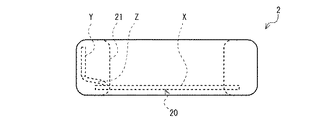
フレキシブルプリント配線板40は、コイル状回路32aが構成されるコイル領域Xを有する。また、フレキシブルプリント配線板40は、導電パターンが受電を制御する回路を構成する領域(部品領域Y)を有する。さらに、フレキシブルプリント配線板40は、コイル領域Xと部品領域Yとを接続する接続領域Zを有する。図5において給電モジュール10のフレキシブルプリント配線板30と同様の構成要素は同一の符号を付し、説明を省略する。<Flexible printed wiring board>
The flexible printed
(コイル領域)
コイル領域Xは、給電モジュール10のフレキシブルプリント配線板30のコイル領域Xと同様に構成できる。電力伝送効率の観点から給電モジュール10及び受電モジュール20は、同一形状のコイル領域Xを有するフレキシブルプリント配線板を備えるとよい。(Coil area)
The coil area X can be configured similarly to the coil area X of the flexible printed
なお、給電モジュール10のフレキシブルプリント配線板30のコイル状回路32a及び受電モジュール20のフレキシブルプリント配線板40のコイル状回路32aの導体の平均幅、導体間ピッチ及び巻数は、給電モジュール10及び受電モジュール20のインダクタンスが共振周波数や電流が所望の値となるように調整するとよい。すなわち、給電モジュール10と受電モジュール20とで、コイル状回路32aの導体の平均幅、導体間ピッチ及び巻数は異なる値となってもよい。
The average width, the inter-conductor pitch, and the number of turns of the conductors of the coiled
(部品領域)
部品領域Yには、受電を制御するための電子部品が実装され、導電パターンにより上記電子部品が接続される。(Parts area)
In the component area Y, an electronic component for controlling power reception is mounted, and the electronic component is connected by a conductive pattern.
上記電子部品は、電気的に機能する部品であり、例えばコネクター、抵抗、キャパシタ、センサ、IC(Integrated Circuit)等を含む。特に、製品の一層の小型化を可能とするため、電子部品として部品領域Yに電力制御等をするICなどの制御回路を組み込むとよい。 The electronic component is a component that functions electrically, and includes, for example, a connector, a resistor, a capacitor, a sensor, an IC (Integrated Circuit), and the like. In particular, in order to further reduce the size of the product, it is preferable to incorporate a control circuit such as an IC that performs power control or the like in the component region Y as an electronic component.
部品領域Yはウエアラブルデバイス2の突出部に配設されている。このように部品領域Yを湾曲していない上記突出部に配設することで、部品領域Yの電子部品を湾曲して配設する必要がないため、上記電子部品に対して可撓性を不要とできる。このため、部品領域Yの部品等に対する設計制約の増加を抑止できる。
The component region Y is disposed on the protruding portion of the
(接続領域)
接続領域Zは、コイル領域Xと部品領域Yとに連結され、導電パターンがコイル領域Xと部品領域Yとの回路間を電気的に接続する領域である。(Connection area)
The connection region Z is a region that is connected to the coil region X and the component region Y, and the conductive pattern electrically connects the circuits of the coil region X and the component region Y.
コイル領域X、部品領域Y、及び接続領域Zは、1枚のフレキシブルプリント配線板上に設けてもよいが、領域毎に異なるフレキシブルプリント配線板を用いてもよい。1枚のフレキシブルプリント配線板で構成する場合、フレキシブルプリント配線板の立体的な曲折により、コイル領域X、部品領域Y、及び接続領域Zを構成することができる。また、各領域を異なるフレキシブルプリント配線板で構成する場合、フレキシブルプリント配線板間の接続方法としては、公知の方法を用いることができる。このような公知の方法としては、例えばバンプ接続、金属ペーストの焼成、異方性導電膜を用いた圧着、導体の溶接等を挙げることができる。 The coil region X, the component region Y, and the connection region Z may be provided on one flexible printed wiring board, but different flexible printed wiring boards may be used for each region. In the case of a single flexible printed wiring board, the coil region X, the component region Y, and the connection region Z can be formed by three-dimensional bending of the flexible printed wiring board. Moreover, when each area | region is comprised with a different flexible printed wiring board, a well-known method can be used as a connection method between flexible printed wiring boards. Examples of such known methods include bump connection, firing of metal paste, pressure bonding using an anisotropic conductive film, welding of conductors, and the like.
受電モジュール20は、上記貫通孔21を取り囲み、かつフレキシブルプリント配線板40の絶縁フィルムの表面がウエアラブルデバイス2の底面と略平行となるように上記ウエアラブルデバイス2の内部に配設される。また、受電モジュール20は、充電時にコイル状回路32aが絶縁フィルム31よりも給電モジュール10のフレキシブルプリント配線板40に近い面側となるように配設するとよい。このように受電モジュール20を配設することで、絶縁フィルムが電力伝送時に給電モジュール10と受電モジュール20との間の遮蔽物とならず、電力伝送効率の低下を抑止できる。
The
受電モジュール20のフレキシブルプリント配線板40の表面とウエアラブルデバイス2の底面との平均距離の下限としては、0.5mmが好ましく、1mmがより好ましい。一方、当該フレキシブルプリント配線板40の表面とウエアラブルデバイス2の底面との平均距離の上限としては、5mmが好ましく、3mmがより好ましい。当該フレキシブルプリント配線板40の表面とウエアラブルデバイス2の底面との平均距離が上記下限未満である場合、受電モジュール20を覆うウエアラブルデバイス2の肉厚が薄くなり過ぎるため、ウエアラブルデバイス2が強度不足となるおそれがある。逆に、当該フレキシブルプリント配線板40の表面とウエアラブルデバイス2の底面との平均距離が上記上限を超える場合、給電モジュール10から受電モジュール20への電力伝送効率が低下するおそれがある。
The lower limit of the average distance between the surface of the flexible printed
上記給電モジュール10のフレキシブルプリント配線板30のコイル領域Xと上記受電モジュール20のフレキシブルプリント配線板40のコイル領域Xとは、充電時に対向するよう構成されている。従って、受電モジュール20のコイル状回路32aは、充電時に給電モジュール10のコイル状回路32aが発生する磁束を受け取ることで電流を発生できる。発生した電流は受電制御回路によりこの受電モジュール20が搭載されているウエアラブルデバイス2の電力として利用される。
The coil area X of the flexible printed
充電時に受電モジュール20のフレキシブルプリント配線板40の表面は、凸部12の中心軸と略垂直であるとよい。このように充電時に受電モジュール20のフレキシブルプリント配線板40の表面を凸部12の中心軸と略垂直とすることで、受電モジュール20は給電モジュール10が発生する磁束を効率的に受け取ることができ、電力伝送効率が高まる。ここで「フレキシブルプリント配線板の表面が凸部の中心軸と略垂直である」とは、フレキシブルプリント配線板の表面と凸部の中心軸のなす角度が90°±5°であることを意味する。
The surface of the flexible printed
また、電力伝送効率の観点から、充電時の給電モジュール10のフレキシブルプリント配線板30のコイル領域Xと受電モジュール20のフレキシブルプリント配線板40のコイル領域Xとの平均距離は小さい方がよい。具体的には、充電時の上記コイル領域間の平均距離の上限としては、10mmが好ましく、6mmがさらに好ましい。一方、充電時の上記コイル領域間の平均距離の下限としては、1mmが好ましく、2mmがより好ましい。充電時の上記コイル領域間の平均距離が上記下限未満である場合、充電デバイス1が給電モジュール10を覆う台座部11やウエアラブルデバイス2が受電モジュール20を覆うウエアラブルデバイス2の肉厚が薄くなり過ぎるため、充電デバイス1やウエアラブルデバイス2が強度不足となるおそれがある。ここで、「コイル領域間の平均距離」とは、一方のコイル領域の中心点と他方のコイル領域の中心点との一方のコイル領域の中心軸方向の距離である。
From the viewpoint of power transmission efficiency, the average distance between the coil region X of the flexible printed
充電時の受電モジュール20のコイル領域Xにおける給電モジュール10のコイル領域Xの投影面積の割合の下限としては、90%が好ましく、95%がより好ましい。上記投影面積の割合が上記下限未満である場合、電力伝送効率が低下するおそれがある。ここで、「受電モジュールのコイル領域における給電モジュールのコイル領域の投影面積の割合」とは、受電モジュールのコイル領域面積に対する受電モジュールのコイル領域に重複する給電モジュールの投影領域の面積の比である。
The lower limit of the ratio of the projected area of the coil area X of the
<フレキシブルプリント配線板の製造方法>
当該フレキシブルプリント配線板30、40は、導電パターン形成工程、カバーレイ積層工程及び磁性体層積層工程を備える製造方法によって容易かつ確実に製造できる。<Method for producing flexible printed wiring board>
The flexible printed
(導電パターン形成工程)
まず、導電パターン形成工程において、絶縁フィルム31に導電材料を積層して導電パターン32を形成する。導電パターン32のコイル状回路32aの平面形状は、導電性材料の積層方法等に応じて適当な方法により形成できる。例えば絶縁フィルム31に積層した金属膜にマスキングを施してエッチングすることで、コイル状回路32aを形成できる。この金属膜の形成方法は、例えば金属箔等を絶縁フィルム31に接着剤等により貼り着けてもよく、絶縁フィルム31に金属を蒸着して形成してもよい。また、導電パターン32を導電性ペーストで形成する場合には、印刷技術によってコイル状回路32aを形成できる。(Conductive pattern formation process)
First, in the conductive pattern forming process, a conductive material is laminated on the insulating
(カバーレイ積層工程)
次に、カバーレイ積層工程において、導電パターン32の表面にカバーレイ35を積層する。具体的には、カバーレイ35は、導電パターン32にカバーフィルム接着層35bを介してカバーフィルム35aを貼り着けることで形成できる。(Coverlay lamination process)
Next, in the cover lay stacking step, the cover lay 35 is stacked on the surface of the
(磁性体層積層工程)
最後に、磁性体層積層工程において、絶縁フィルム31の裏面に磁性体層33を積層する。具体的には、磁性体層33は、絶縁フィルム31に磁性体接着層34を介して磁性体シートを貼り着けることで形成できる。(Magnetic layer lamination process)
Finally, in the magnetic layer stacking step, the
以上のようにして製造された当該フレキシブルプリント配線板30、40は、充電デバイス1及びウエアラブルデバイス2に固定され、それぞれの制御回路と接続され、当該非接触充電システムを構成することができる。
The flexible printed
<使用方法>
次に、当該非接触充電システムの使用方法について説明する。<How to use>
Next, a method for using the contactless charging system will be described.
当該非接触充電システムでは、例えば受電モジュール20を付設したウエアラブルデバイス2に対して充電デバイス1の給電モジュール10から電力伝送を行う。
In the non-contact charging system, for example, power is transmitted from the
当該非接触充電システムによる給電では、まずウエアラブルデバイス2をウエアラブルデバイス2の貫通孔21が充電デバイス1の凸部12に嵌合するように台座部11の上面に載置する。このとき、図3に示すように給電モジュール10のコイル領域Xと受電モジュール20のコイル領域Xとが対向する。
In the power supply by the non-contact charging system, first, the
ウエアラブルデバイス2の載置後、電流供給回路により給電モジュール10のコイル状回路32aに電流を供給する。これにより給電モジュール10のコイル状回路32aに磁束が発生し、この磁束が対向する受電モジュール20のコイル状回路32aを貫通する。磁束が貫通した受電モジュール20のコイル状回路32aには、この磁束を打ち消す磁束を生成するための電流が発生し、この電流により例えばウエアラブルデバイス2内の充電池に給電が行われる。
After the
<利点>
当該非接触充電システムは、給電モジュール10及び受電モジュール20がコイル領域Xを有するフレキシブルプリント配線板30、40を備える。フレキシブルプリント配線板30、40は薄膜化及び微細化が可能であり、かつ曲折により湾曲面に配設できるため、当該非接触充電システムは、給電モジュール10及び受電モジュール20の小型化が容易である。従って、当該非接触充電システムは、ウエアラブルデバイス2に適用が容易である。さらに、当該非接触充電システムは、上記コイル領域Xが円環状であるので、中央の空間が磁界の通り道となり、給電モジュール10及び受電モジュール20のコイルの回路長や導体面積に対してインダクタンスを大きくできる。従って、給電モジュール10及び受電モジュール20がコイル領域Xを有する当該フレキシブルプリント配線板30、40を備える当該非接触充電システムは、ウエアラブルデバイスへの適用が容易である。<Advantages>
In the non-contact charging system, the
[その他の実施形態]
今回開示された実施の形態はすべての点で例示であって制限的なものではないと考えられるべきである。本発明の範囲は、上記実施形態の構成に限定されるものではなく、請求の範囲によって示され、請求の範囲と均等の意味及び範囲内での全ての変更が含まれることが意図される。[Other Embodiments]
The embodiment disclosed this time should be considered as illustrative in all points and not restrictive. The scope of the present invention is not limited to the configuration of the embodiment described above, but is defined by the scope of the claims, and is intended to include all modifications within the meaning and scope equivalent to the scope of the claims.
上記実施形態では、コイル状回路が渦巻き状の導電パターンである場合を説明したが、コイル状回路の導電パターンはこれに限られない。例えば、給電モジュール及び受電モジュールのコイル状回路のいずれか一方又は両方について、導電パターンを多層とし、ソレノイド回路を構成してもよい。 In the above embodiment, the case where the coiled circuit is a spiral conductive pattern has been described, but the conductive pattern of the coiled circuit is not limited to this. For example, for one or both of the coil-like circuits of the power feeding module and the power receiving module, the conductive pattern may be multilayered to constitute a solenoid circuit.
また、上記実施形態では、部品領域をウエアラブルデバイスの突出部に配設したが、ウエアラブルデバイスの突出部以外の上面や底面に配設してもよい。 Moreover, in the said embodiment, although the components area | region was arrange | positioned in the protrusion part of the wearable device, you may arrange | position on upper surfaces and bottom surfaces other than the protrusion part of a wearable device.
上記実施形態では、ウエアラブルデバイスが中央に貫通孔を有し、この貫通孔と凸部が嵌合する場合を説明したが、この凸部が嵌合する部分は、貫通孔でなくともよく、例えば凹部であってもよい。 In the above embodiment, the wearable device has a through-hole in the center, and the case where the through-hole and the convex portion are fitted is described. However, the portion where the convex portion is fitted may not be the through-hole, for example, It may be a recess.
また、上記貫通孔及び凸部の平面形状は、充電デバイスとウエアラブルデバイスとが嵌合できる限り、円でなくともよい。例えば上記平面形状は、楕円状や多角形状であってもよい。 Further, the planar shape of the through hole and the convex portion may not be a circle as long as the charging device and the wearable device can be fitted. For example, the planar shape may be elliptical or polygonal.
また、上記実施形態では、充電デバイスの台座部の平面形状が円である場合を説明したが、上記平面形状が他の形状、例えば楕円や方形状等であってもよい。 Moreover, although the said embodiment demonstrated the case where the planar shape of the base part of a charging device was a circle, the said planar shape may be another shape, for example, an ellipse, a square shape, etc.
さらに、充電デバイスの凸部は必須ではなく、充電時に上記給電モジュールのフレキシブルプリント配線板のコイル領域と上記受電モジュールのフレキシブルプリント配線板のコイル領域とが対向できる限り、その形状は特に限定されない。例えば平面上にウエアラブルデバイスを配設すべき場所が印刷されていてもよい。 Furthermore, the convex part of the charging device is not essential, and the shape thereof is not particularly limited as long as the coil region of the flexible printed wiring board of the power supply module and the coil region of the flexible printed wiring board of the power receiving module can face each other during charging. For example, the place where the wearable device should be arranged on a plane may be printed.
上記実施形態では、フレキシブルプリント配線板が、絶縁フィルムの裏面側に強磁性材料を含む磁性体層を備える場合を説明したが、上記磁性体層は必須の構成要件ではなく、磁性体層を含まないフレキシブルプリント配線板も本発明の意図するところである。 In the said embodiment, although the flexible printed wiring board demonstrated the case where the back surface side of an insulating film was equipped with the magnetic body layer containing a ferromagnetic material, the said magnetic body layer is not an essential structural requirement but contains a magnetic body layer. No flexible printed wiring board is contemplated by the present invention.
上記実施形態ではフレキシブルプリント配線板の絶縁フィルムの一方の面に導電パターンを備える場合を説明したが、フレキシブルプリント配線板が導電パターンを絶縁フィルムの両面に備えてもよい。すなわち、図6に示すようにフレキシブルプリント配線板50のコイル領域が、絶縁フィルム31の一方の面側に積層され第1コイル状回路51aを構成する第1導電パターン51と、上記絶縁フィルム31の第1導電パターン51とは反対の面側に積層され第2コイル状回路52aを構成する第2導電パターン52とを有し、上記第1導電パターン51と上記第2導電パターン52とがスルーホール53により電気的に接続されていてもよい。このように当該フレキシブルプリント配線板50が上記導電パターンを上記絶縁フィルムの両面に備えることにより、当該フレキシブルプリント配線板50の大きさの増加を抑止しつつ、インダクタンスを調整することができる。なお、スルーホール53は貫通孔にメッキを施すことで形成できる。また、銀ペースト、銅ペースト等の導電ペーストを貫通孔に注入して加熱硬化させて形成してもよい。
Although the said embodiment demonstrated the case where a conductive pattern was provided in one surface of the insulating film of a flexible printed wiring board, a flexible printed wiring board may be equipped with the conductive pattern on both surfaces of an insulating film. That is, as shown in FIG. 6, the coil region of the flexible printed wiring board 50 is laminated on one surface side of the insulating
さらに、当該フレキシブルプリント配線板は絶縁フィルムを介して配設され、少なくともコイル状回路を構成する円環状のコイル領域を有する2以上の導電パターンをさらに有し、上記導電パターン間がスルーホールにより電気的に接続してもよい。すなわち、上記実施形態ではフレキシブルプリント配線板の絶縁フィルムの一方の面に導電パターンを備える場合を説明したが、この導電パターンに加え、例えば上記絶縁フィルムの反対側の面に第2の導電パターンを有し、上記第2導電パターンの上記絶縁フィルムとは反対側の面にさらに絶縁フィルムを介して第3の導電パターンを有する構成としてもよい。この第2導電パターン及び第3導電パターンはコイル状回路を構成する円環状のコイル領域を有し、導電パターン間がスルーホールにより電気的に接続される。このような構成とすることで、当該フレキシブルプリント配線板は大きさの増加を抑止しつつ、インダクタンスをさらに大きくすることができる。なお、この構成は、合計で3つの導電パターンを有するが、当該フレキシブルプリント配線板は、合計で4つ以上の導電パターンを有する構成とすることもできる。 Furthermore, the flexible printed wiring board further includes two or more conductive patterns having an annular coil region constituting at least a coil-shaped circuit, which is disposed via an insulating film, and the conductive patterns are electrically connected by a through hole. May be connected. That is, in the above embodiment, the case where the conductive pattern is provided on one surface of the insulating film of the flexible printed wiring board has been described. In addition to this conductive pattern, for example, the second conductive pattern is provided on the opposite surface of the insulating film. It is good also as a structure which has a 3rd conductive pattern through the insulating film further on the surface on the opposite side to the said insulating film of the said 2nd conductive pattern. The second conductive pattern and the third conductive pattern have an annular coil region constituting a coiled circuit, and the conductive patterns are electrically connected by through holes. By setting it as such a structure, the said flexible printed wiring board can further increase an inductance, suppressing the increase in a magnitude | size. In addition, although this structure has a total of three conductive patterns, the said flexible printed wiring board can also be set as the structure which has a total of four or more conductive patterns.
また、絶縁フィルムの一方の面に導電パターンを備えるフレキシブルプリント配線板を2枚用意し、その裏面同士を磁性体層を挟んで磁性体接着層を介して接着することでフレキシブルプリント配線板のコイル領域を構成してもよい。このような構成とすることで、磁性体によるインダクタンスの増大効果と、給電モジュール及び受電モジュールの大きさの増加を抑止しつつ、インダクタンスを調整する効果とを同時に実現することができる。 In addition, two flexible printed wiring boards having a conductive pattern on one surface of an insulating film are prepared, and the back surfaces thereof are bonded to each other via a magnetic material adhesive layer with a magnetic material layer sandwiched between them. An area may be configured. With such a configuration, it is possible to simultaneously achieve the effect of increasing the inductance due to the magnetic material and the effect of adjusting the inductance while suppressing the increase in size of the power supply module and the power receiving module.
1 充電デバイス
2 ウエアラブルデバイス
10 給電モジュール
11 台座部
12 凸部
20 受電モジュール
21 貫通孔
30、40 フレキシブルプリント配線板
31 絶縁フィルム
32 導電パターン
32a コイル状回路
33 磁性体層
34 磁性体接着層
35 カバーレイ
35a カバーフィルム
35b カバーフィルム接着層
51 第1導電パターン
52 第2導電パターン
51a 第1コイル状回路
52a 第2コイル状回路
53 スルーホール
X コイル領域
Y 部品領域
Z 接続領域DESCRIPTION OF
Claims (7)
上記導電パターンがコイル状回路を構成する円環状のコイル領域と、
上記コイル領域の外部に配設され、かつ上記コイル領域の導電パターンと電気的に接続される電子部品を有する部品領域とを有するフレキシブルプリント配線板。A flexible printed wiring board having an insulating film and a conductive pattern laminated on at least one surface side of the insulating film,
An annular coil region in which the conductive pattern forms a coiled circuit;
A flexible printed wiring board having an electronic component disposed outside the coil region and having an electronic component electrically connected to the conductive pattern of the coil region.
上記導電パターン間がスルーホールにより電気的に接続されている請求項1、請求項2又は請求項3に記載のフレキシブルプリント配線板。It further includes two or more conductive patterns that are arranged via an insulating film and have at least an annular coil region that constitutes a coiled circuit,
The flexible printed wiring board according to claim 1, wherein the conductive patterns are electrically connected by through holes.
環状のウエアラブルデバイスに付設される受電モジュールと
を備える非接触充電システムであって、
上記給電モジュール及び上記受電モジュールそれぞれが、請求項1に記載のフレキシブルプリント配線板を備え、
充電時に上記給電モジュールのフレキシブルプリント配線板のコイル領域と上記受電モジュールのフレキシブルプリント配線板のコイル領域とが対向するよう構成されている非接触充電システム。A power supply module attached to the charging device;
A non-contact charging system comprising a power receiving module attached to an annular wearable device,
Each of the power feeding module and the power receiving module includes the flexible printed wiring board according to claim 1,
A non-contact charging system configured such that a coil region of the flexible printed wiring board of the power supply module and a coil region of the flexible printed wiring board of the power receiving module face each other during charging.
Applications Claiming Priority (3)
| Application Number | Priority Date | Filing Date | Title |
|---|---|---|---|
| JP2015185733 | 2015-09-18 | ||
| JP2015185733 | 2015-09-18 | ||
| PCT/JP2016/076488 WO2017047498A1 (en) | 2015-09-18 | 2016-09-08 | Flexible printed wiring board and contactless charging system |
Publications (1)
| Publication Number | Publication Date |
|---|---|
| JPWO2017047498A1 true JPWO2017047498A1 (en) | 2018-07-05 |
Family
ID=58289184
Family Applications (1)
| Application Number | Title | Priority Date | Filing Date |
|---|---|---|---|
| JP2017539868A Pending JPWO2017047498A1 (en) | 2015-09-18 | 2016-09-08 | Flexible printed wiring board and non-contact charging system |
Country Status (2)
| Country | Link |
|---|---|
| JP (1) | JPWO2017047498A1 (en) |
| WO (1) | WO2017047498A1 (en) |
Families Citing this family (4)
| Publication number | Priority date | Publication date | Assignee | Title |
|---|---|---|---|---|
| US20200367360A1 (en) * | 2017-07-06 | 2020-11-19 | Sumitomo Electric Printed Circuits, Inc. | Flexible printed wiring board |
| JP7509502B2 (en) * | 2017-11-28 | 2024-07-02 | 住友電工プリントサーキット株式会社 | Manufacturing method of flexible printed wiring board and flexible printed wiring board |
| CN214337578U (en) * | 2020-10-31 | 2021-10-01 | 荣耀终端有限公司 | Wearables and Wearable Systems |
| JP7524844B2 (en) * | 2021-06-30 | 2024-07-30 | トヨタ自動車株式会社 | Power supply mat |
Family Cites Families (8)
| Publication number | Priority date | Publication date | Assignee | Title |
|---|---|---|---|---|
| KR101390746B1 (en) * | 2006-08-04 | 2014-05-02 | 에스케이케미칼주식회사 | Induction coil for cordless energy charging and data transfer |
| JP4412402B2 (en) * | 2007-02-20 | 2010-02-10 | セイコーエプソン株式会社 | Coil unit and electronic equipment |
| JP2008205215A (en) * | 2007-02-20 | 2008-09-04 | Seiko Epson Corp | Multilayer coil unit and electronic device and charger using the same |
| JP2011187559A (en) * | 2010-03-05 | 2011-09-22 | Tsuchiya Co Ltd | Contactless power transmission film |
| JP5965148B2 (en) * | 2012-01-05 | 2016-08-03 | 日東電工株式会社 | Power receiving module for mobile terminal using wireless power transmission and rechargeable battery for mobile terminal equipped with power receiving module for mobile terminal |
| JP6313744B2 (en) * | 2012-03-23 | 2018-04-18 | エルジー イノテック カンパニー リミテッド | Wireless power receiver |
| JP2015142395A (en) * | 2014-01-27 | 2015-08-03 | 住友電工プリントサーキット株式会社 | power supply device |
| JP2016134598A (en) * | 2015-01-22 | 2016-07-25 | ヒタチ−エルジー データ ストレージ コリア,インコーポレイティド | Wireless charging receiver |
-
2016
- 2016-09-08 JP JP2017539868A patent/JPWO2017047498A1/en active Pending
- 2016-09-08 WO PCT/JP2016/076488 patent/WO2017047498A1/en not_active Ceased
Also Published As
| Publication number | Publication date |
|---|---|
| WO2017047498A1 (en) | 2017-03-23 |
Similar Documents
| Publication | Publication Date | Title |
|---|---|---|
| JPWO2017038797A1 (en) | Flexible printed wiring board and non-contact charging system | |
| JP6286800B2 (en) | Printed wiring board, antenna and wireless power feeder | |
| CN208796795U (en) | Coil block | |
| JP6146531B2 (en) | Mobile device | |
| JP6008237B2 (en) | Mobile device | |
| JP5832693B2 (en) | Secondary coil of receiver for contactless charging system | |
| KR101452093B1 (en) | Thin film coil, shield part including the same, and contactless power transmission device having the shield part | |
| JP2010041906A (en) | Contactless power transmission apparatus, soft magnetic sheet, and module using the same | |
| JP5364745B2 (en) | Magnetic element for wireless power transmission and power supply device | |
| JP6008236B2 (en) | Mobile device | |
| WO2013121729A1 (en) | Contactless charging module and mobile terminal provided with same | |
| JP2014112728A (en) | Thin film coil and electronic device having the same | |
| JP2015149405A (en) | Antenna device, antenna unit for non-contact power transmission, and electronic device | |
| US20190252768A1 (en) | Antenna module and electronic device having the same | |
| JPWO2017047498A1 (en) | Flexible printed wiring board and non-contact charging system | |
| WO2019009269A1 (en) | Flexible printed wiring board | |
| WO2019111848A1 (en) | Coil module | |
| JP2016025502A (en) | Wireless power receiving antenna and wearable device | |
| JP6231061B2 (en) | Receiving coil unit of non-contact power feeding device and manufacturing method thereof | |
| JPWO2017057116A1 (en) | Flexible printed wiring board for solenoid coil, solenoid coil and wearable device | |
| JPWO2017057115A1 (en) | Flexible printed wiring board for solenoid coil, solenoid coil and wearable device | |
| TWM502239U (en) | Thin-film coil component and charging apparatus |