JPWO2015040971A1 - Image display device - Google Patents
Image display device Download PDFInfo
- Publication number
- JPWO2015040971A1 JPWO2015040971A1 JP2015537597A JP2015537597A JPWO2015040971A1 JP WO2015040971 A1 JPWO2015040971 A1 JP WO2015040971A1 JP 2015537597 A JP2015537597 A JP 2015537597A JP 2015537597 A JP2015537597 A JP 2015537597A JP WO2015040971 A1 JPWO2015040971 A1 JP WO2015040971A1
- Authority
- JP
- Japan
- Prior art keywords
- data
- ramp signal
- value
- line
- analog switches
- Prior art date
- Legal status (The legal status is an assumption and is not a legal conclusion. Google has not performed a legal analysis and makes no representation as to the accuracy of the status listed.)
- Pending
Links
Images


Classifications
-
- G—PHYSICS
- G09—EDUCATION; CRYPTOGRAPHY; DISPLAY; ADVERTISING; SEALS
- G09G—ARRANGEMENTS OR CIRCUITS FOR CONTROL OF INDICATING DEVICES USING STATIC MEANS TO PRESENT VARIABLE INFORMATION
- G09G3/00—Control arrangements or circuits, of interest only in connection with visual indicators other than cathode-ray tubes
- G09G3/20—Control arrangements or circuits, of interest only in connection with visual indicators other than cathode-ray tubes for presentation of an assembly of a number of characters, e.g. a page, by composing the assembly by combination of individual elements arranged in a matrix no fixed position being assigned to or needed to be assigned to the individual characters or partial characters
- G09G3/34—Control arrangements or circuits, of interest only in connection with visual indicators other than cathode-ray tubes for presentation of an assembly of a number of characters, e.g. a page, by composing the assembly by combination of individual elements arranged in a matrix no fixed position being assigned to or needed to be assigned to the individual characters or partial characters by control of light from an independent source
- G09G3/36—Control arrangements or circuits, of interest only in connection with visual indicators other than cathode-ray tubes for presentation of an assembly of a number of characters, e.g. a page, by composing the assembly by combination of individual elements arranged in a matrix no fixed position being assigned to or needed to be assigned to the individual characters or partial characters by control of light from an independent source using liquid crystals
- G09G3/3607—Control arrangements or circuits, of interest only in connection with visual indicators other than cathode-ray tubes for presentation of an assembly of a number of characters, e.g. a page, by composing the assembly by combination of individual elements arranged in a matrix no fixed position being assigned to or needed to be assigned to the individual characters or partial characters by control of light from an independent source using liquid crystals for displaying colours or for displaying grey scales with a specific pixel layout, e.g. using sub-pixels
-
- G—PHYSICS
- G09—EDUCATION; CRYPTOGRAPHY; DISPLAY; ADVERTISING; SEALS
- G09G—ARRANGEMENTS OR CIRCUITS FOR CONTROL OF INDICATING DEVICES USING STATIC MEANS TO PRESENT VARIABLE INFORMATION
- G09G3/00—Control arrangements or circuits, of interest only in connection with visual indicators other than cathode-ray tubes
- G09G3/20—Control arrangements or circuits, of interest only in connection with visual indicators other than cathode-ray tubes for presentation of an assembly of a number of characters, e.g. a page, by composing the assembly by combination of individual elements arranged in a matrix no fixed position being assigned to or needed to be assigned to the individual characters or partial characters
- G09G3/34—Control arrangements or circuits, of interest only in connection with visual indicators other than cathode-ray tubes for presentation of an assembly of a number of characters, e.g. a page, by composing the assembly by combination of individual elements arranged in a matrix no fixed position being assigned to or needed to be assigned to the individual characters or partial characters by control of light from an independent source
- G09G3/3406—Control of illumination source
- G09G3/342—Control of illumination source using several illumination sources separately controlled corresponding to different display panel areas, e.g. along one dimension such as lines
- G09G3/3426—Control of illumination source using several illumination sources separately controlled corresponding to different display panel areas, e.g. along one dimension such as lines the different display panel areas being distributed in two dimensions, e.g. matrix
-
- G—PHYSICS
- G09—EDUCATION; CRYPTOGRAPHY; DISPLAY; ADVERTISING; SEALS
- G09G—ARRANGEMENTS OR CIRCUITS FOR CONTROL OF INDICATING DEVICES USING STATIC MEANS TO PRESENT VARIABLE INFORMATION
- G09G2300/00—Aspects of the constitution of display devices
- G09G2300/08—Active matrix structure, i.e. with use of active elements, inclusive of non-linear two terminal elements, in the pixels together with light emitting or modulating elements
- G09G2300/0809—Several active elements per pixel in active matrix panels
- G09G2300/0828—Several active elements per pixel in active matrix panels forming a digital to analog [D/A] conversion circuit
-
- G—PHYSICS
- G09—EDUCATION; CRYPTOGRAPHY; DISPLAY; ADVERTISING; SEALS
- G09G—ARRANGEMENTS OR CIRCUITS FOR CONTROL OF INDICATING DEVICES USING STATIC MEANS TO PRESENT VARIABLE INFORMATION
- G09G2310/00—Command of the display device
- G09G2310/02—Addressing, scanning or driving the display screen or processing steps related thereto
- G09G2310/024—Scrolling of light from the illumination source over the display in combination with the scanning of the display screen
-
- G—PHYSICS
- G09—EDUCATION; CRYPTOGRAPHY; DISPLAY; ADVERTISING; SEALS
- G09G—ARRANGEMENTS OR CIRCUITS FOR CONTROL OF INDICATING DEVICES USING STATIC MEANS TO PRESENT VARIABLE INFORMATION
- G09G2310/00—Command of the display device
- G09G2310/02—Addressing, scanning or driving the display screen or processing steps related thereto
- G09G2310/0243—Details of the generation of driving signals
- G09G2310/0259—Details of the generation of driving signals with use of an analog or digital ramp generator in the column driver or in the pixel circuit
-
- G—PHYSICS
- G09—EDUCATION; CRYPTOGRAPHY; DISPLAY; ADVERTISING; SEALS
- G09G—ARRANGEMENTS OR CIRCUITS FOR CONTROL OF INDICATING DEVICES USING STATIC MEANS TO PRESENT VARIABLE INFORMATION
- G09G2310/00—Command of the display device
- G09G2310/02—Addressing, scanning or driving the display screen or processing steps related thereto
- G09G2310/0264—Details of driving circuits
- G09G2310/027—Details of drivers for data electrodes, the drivers handling digital grey scale data, e.g. use of D/A converters
-
- G—PHYSICS
- G09—EDUCATION; CRYPTOGRAPHY; DISPLAY; ADVERTISING; SEALS
- G09G—ARRANGEMENTS OR CIRCUITS FOR CONTROL OF INDICATING DEVICES USING STATIC MEANS TO PRESENT VARIABLE INFORMATION
- G09G2320/00—Control of display operating conditions
- G09G2320/02—Improving the quality of display appearance
- G09G2320/0271—Adjustment of the gradation levels within the range of the gradation scale, e.g. by redistribution or clipping
-
- G—PHYSICS
- G09—EDUCATION; CRYPTOGRAPHY; DISPLAY; ADVERTISING; SEALS
- G09G—ARRANGEMENTS OR CIRCUITS FOR CONTROL OF INDICATING DEVICES USING STATIC MEANS TO PRESENT VARIABLE INFORMATION
- G09G2320/00—Control of display operating conditions
- G09G2320/02—Improving the quality of display appearance
- G09G2320/0285—Improving the quality of display appearance using tables for spatial correction of display data
Landscapes
- Engineering & Computer Science (AREA)
- Physics & Mathematics (AREA)
- Computer Hardware Design (AREA)
- General Physics & Mathematics (AREA)
- Theoretical Computer Science (AREA)
- Chemical & Material Sciences (AREA)
- Crystallography & Structural Chemistry (AREA)
- Control Of Indicators Other Than Cathode Ray Tubes (AREA)
- Liquid Crystal (AREA)
- Liquid Crystal Display Device Control (AREA)
Abstract
画像表示装置(100)は、変換用アナログ信号発生部(101)を備える。ヒストグラム値出力部(206a,206b)は、1ラインの各画素の画像データが有するヒストグラム値データを出力する。累積加算器(210a,210b)は、ヒストグラム値データを累積加算する。累積加算値は、複数のアナログスイッチ(1071〜107n)のうちオフされたアナログスイッチ数を示す。ランプ信号データ生成部(213)は、オフされたアナログスイッチ数の大小に起因する負荷変動によって、ランプ信号の電圧変動を抑圧するように、累積加算値に応じて傾斜の程度が可変制御された非線形の傾斜を示すランプ信号データを生成する。DA変換部(214)は、ランプ信号データをアナログ信号のランプ信号に変換して、複数のアナログスイッチ(1071〜107n)に供給する。The image display device (100) includes a conversion analog signal generation unit (101). The histogram value output units (206a, 206b) output histogram value data included in the image data of each pixel of one line. The cumulative adders (210a, 210b) cumulatively add histogram value data. The cumulative addition value indicates the number of analog switches turned off among the plurality of analog switches (1071 to 107n). In the ramp signal data generation unit (213), the degree of inclination is variably controlled in accordance with the accumulated addition value so as to suppress the voltage variation of the ramp signal due to the load variation caused by the magnitude of the number of analog switches turned off. Ramp signal data indicating a non-linear slope is generated. The DA converter (214) converts the ramp signal data into an analog ramp signal and supplies it to the plurality of analog switches (1071 to 107n).
Description
本開示は、デジタル映像信号をランプ信号などを使ってデジタル−アナログ変換(以下、DA変換)して得たアナログ電圧で表示素子を駆動して画像表示を行う画像表示装置に関する。 The present disclosure relates to an image display apparatus that displays an image by driving a display element with an analog voltage obtained by digital-analog conversion (hereinafter referred to as DA conversion) of a digital video signal using a ramp signal or the like.
近年、画像表示装置として液晶を用いた表示パネル装置(液晶表示装置)の躍進が著しい。液晶表示装置は、ビデオカメラのビューファインダや液晶表示パネル、自動車用のテレビや、ナビゲーションシステムの表示パネル、ノート型パソコンのディスプレイ等に広く使われている。 In recent years, the progress of display panel devices (liquid crystal display devices) using liquid crystals as image display devices has been remarkable. Liquid crystal display devices are widely used in video camera viewfinders, liquid crystal display panels, automobile televisions, navigation system display panels, notebook computer displays, and the like.
液晶表示装置は、本来アナログ映像信号を表示する装置である。高精細度、高画質の液晶表示装置の駆動回路は、非常に大規模で、多数のチップを必要とし、かつ精度の高い回路が必要とされる。表示パネルのコストの制約は、表示画質を決定する大きな要素の一つとなっている。 The liquid crystal display device is a device that originally displays an analog video signal. The driving circuit of a high-definition and high-quality liquid crystal display device is very large, requires a large number of chips, and requires a highly accurate circuit. The cost limitation of the display panel is one of the major factors that determine the display image quality.
近年、周辺回路のデジタル化が進み、それに伴い、映像信号としてデジタルデータを液晶素子に入力するのがシステム全体として好都合である。そこで、表示パネルのコストの制約を満足するためにも、回路規模を増大させずに高画質化を実現するために、デジタル映像信号をアナログ映像信号に変換するDA変換回路を備える画像表示装置が提案されている(特許文献1参照)。 In recent years, digitalization of peripheral circuits has progressed, and accordingly, it is convenient for the entire system to input digital data as a video signal to a liquid crystal element. Accordingly, an image display device including a DA conversion circuit that converts a digital video signal into an analog video signal in order to achieve high image quality without increasing the circuit scale in order to satisfy the cost constraints of the display panel. It has been proposed (see Patent Document 1).
特許文献1記載の従来の画像表示装置では、1ラインの画素数に等しい数のビデオスイッチ(アナログスイッチ)を各水平走査期間の初めで同時にすべてオンとし、黒から白までの全映像信号の成分を持った単純な1水平走査期間周期のランプ信号を、アナログスイッチを介してデータ線に供給する。
In the conventional image display device described in
カウンタが所定周波数のクロックでカウントし、1水平走査期間内で最小値から最大値まで順次変化するカウンタ値を出力する。 The counter counts with a clock having a predetermined frequency, and outputs a counter value that sequentially changes from the minimum value to the maximum value within one horizontal scanning period.
コンパレータは、1水平走査期間内で表示される映像信号の各画素のデジタルデータとカウンタのカウンタ値とを画素単位で比較して、一致パルスを出力する。コンパレータに対応して設けられたアナログスイッチは、一致パルスによって、一致パルス出力時点以降継続してオフとされる。 The comparator compares the digital data of each pixel of the video signal displayed within one horizontal scanning period with the counter value of the counter for each pixel, and outputs a coincidence pulse. The analog switch provided corresponding to the comparator is continuously turned off by the coincidence pulse after the coincidence pulse is output.
アナログスイッチのオフ時点直前のランプ信号のレベルがサンプルホールドされて、画素に供給される。これによって、デジタルデータの映像信号がアナログ映像信号へと変換される。 The level of the ramp signal immediately before the analog switch is turned off is sampled and held and supplied to the pixel. As a result, the video signal of digital data is converted into an analog video signal.
特許文献1記載の液晶表示装置は、基準となるランプ信号に基づいて、デジタルデータに応じた所定の電圧をサンプルホールドする方式である。
The liquid crystal display device described in
特許文献1記載の液晶表示装置は、回路規模を増大させずに高画質化を実現できるという利点を有する。
The liquid crystal display device described in
しかしながら、表示する絵柄によっては複数の画素で同時に同じ電圧をサンプルホールドしたり、あるいは、全くサンプルホールドされない電圧があったりして、ランプ信号に対する負荷状態が大きく変化することが多い。よって、負荷状態の変化によって、表示画像にストリーキングと称される階調劣化を発生させてしまうという課題がある。 However, depending on the picture to be displayed, the same voltage is sampled and held at a plurality of pixels at the same time or there is a voltage that is not sampled and held at all. Therefore, there is a problem that gradation change called streaking occurs in the display image due to a change in the load state.
図15A,図15Bは、元画像と階調劣化が生じた表示画像の一例を示す。図15Aに示す元画像は、黒背景であるイメージ1a上に50%グレー階調のボックス(イメージ2a)と、イメージ2aと同一階調であり、かつ、水平方向に長いボックス(イメージ3a)とが配置された画像である。図15Aにおいては、50%グレー階調であるイメージ2a及び3aを白で表現している。
FIG. 15A and FIG. 15B show an example of a display image in which gradation deterioration has occurred with the original image. The original image shown in FIG. 15A includes a box (
この元画像を液晶表示装置で表示すると、図15Bに示すような画像が表示される。図15Bに示す表示画像は、黒背景であるイメージ1b上にグレー階調のボックス(イメージ2b)と、イメージ2bと本来同一階調であるにもかかわらず、若干明るさが暗い水平方向に長いボックス(イメージ3b)とが配置された画像となる。
When this original image is displayed on the liquid crystal display device, an image as shown in FIG. 15B is displayed. The display image shown in FIG. 15B has a gray gradation box (
表示画像が図15Bのようになるのは、イメージ3bの方がイメージ2bよりもグレー階調の水平方向の幅が広いため、1水平走査期間で同時にオフになっているアナログスイッチの数が少ないためである。
The display image is as shown in FIG. 15B because the horizontal width of the gray gradation is wider in the
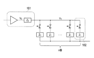
その原因を図16及び図17を用いて説明する。図16は、特許文献1記載の液晶表示装置の要部の一例の等価回路図を示す。図16において、変換用アナログ信号発生回路の出力等価回路161は、デジタルデータのランプ信号データをアナログ信号のランプ信号に変換するDA変換器の内部のバッファとその出力インピーダンスZ0を示す。変換用アナログ信号発生回路の出力側にはn個のアナログスイッチが並列に接続されている。The cause will be described with reference to FIGS. FIG. 16 shows an equivalent circuit diagram of an example of a main part of the liquid crystal display device described in
ここで、n個のアナログスイッチは画面水平方向の画素数に対応しており、各水平走査期間の始めにすべてオンとされる。 Here, n analog switches correspond to the number of pixels in the horizontal direction of the screen, and are all turned on at the beginning of each horizontal scanning period.
デジタル映像信号の各画素値と1水平走査期間内で最小値から最大値までカウントアップするn個のカウンタ(図示せず)のカウンタ値とが比較される。カウンタは、両者が一致したときに一致パルスを出力する。一致パルスによって、カウンタ値が一致したカウンタに対応した画素位置のアナログスイッチが次の水平走査期間の始めまでの期間オフとされる。 Each pixel value of the digital video signal is compared with the counter values of n counters (not shown) that count up from the minimum value to the maximum value within one horizontal scanning period. The counter outputs a coincidence pulse when the two coincide. Due to the coincidence pulse, the analog switch at the pixel position corresponding to the counter with the coincidence counter value is turned off for the period until the beginning of the next horizontal scanning period.
アナログスイッチは、1水平走査期間の最初に最小階調値から開始して1水平走査期間の終了直前に最大階調値に達するレベルのランプ信号をオフ時にサンプリングし、サンプリングしたランプ信号電圧を、対応する画素回路に出力する。 The analog switch samples a ramp signal having a level starting at the minimum gradation value at the beginning of one horizontal scanning period and reaching the maximum gradation value immediately before the end of one horizontal scanning period when the sampled signal is off. Output to the corresponding pixel circuit.
図16において、各アナログスイッチの等価回路162は、1個のアナログスイッチと入力インピーダンスZ1との直列回路で表される。V0はデジタルデータのランプ信号データからアナログ信号のランプ信号を生成するDA変換器内のバッファの出力電圧、V1はDA変換器から出力されてn個のアナログスイッチへ共通に供給されるアナログのランプ信号の入力電圧である。In FIG. 16, the
ここで、あるタイミングで同時にオフになっているアナログスイッチの数をs個としたときのアナログスイッチの入力電圧V1(s)は次の式(1)で表せる。式(1)において、0≦s≦nである。
V1(s)=[Z1/{(n−s)Z0+Z1}]V0 …(1)Here, the input voltage V 1 (s) of the analog switch when the number of analog switches that are simultaneously turned off at a certain timing is s can be expressed by the following equation (1). In the formula (1), 0 ≦ s ≦ n.
V 1 (s) = [Z 1 / {(ns) Z 0 + Z 1 }] V 0 (1)
図15Bに示す黒い背景(イメージ1b)はV0=0であるので、式(1)によれば、アナログスイッチの入力電圧V1は0ボルトである。Since the black background (
Z0=1、Z1=100、n=256とし、図15Bに示す50%グレー階調のイメージ2bの水平幅を64画素、50%グレー階調のイメージ3bの水平幅を128画素とする。このとき、イメージ2b表示時に同時にオフとされるアナログスイッチ数sは192(=256−64)、イメージ3bの表示時に同時にオフとされるアナログスイッチ数sは128(=256−128)となる。
オフとされるアナログスイッチ数sをアナログスイッチオフ数sと称する場合がある。Z 0 = 1, Z 1 = 100, n = 256, the horizontal width of the
The number of analog switches s that are turned off may be referred to as analog switch-off number s.
50%グレーの画像のときの本来のバッファ出力電圧V0は0.5であるとする。Assume that the original buffer output voltage V 0 for a 50% gray image is 0.5.
このとき、式(1)から、イメージ2bの表示時のアナログスイッチの入力電圧V1(192)は0.305、イメージ3bの表示時のアナログスイッチの入力電圧V1(128)は0.219である。At this time, from the expression (1), the input voltage V 1 (192) of the analog switch when the
従って、本来同一階調で表示されるべきイメージ2bとイメージ3bとは、水平方向のグレー階調のイメージの水平幅が互いに異なることから同時にオフとされるアナログスイッチ数sが異なり、その結果、上記のように階調差が生じる。
Therefore, the
また、イメージ2b及び3bのいずれの表示も、入力電圧V1は0.5(50%)となるべきであるが、低い階調表示となることが分かる。Also, any display of
以上から、1ライン表示期間(1水平走査期間)におけるアナログスイッチオフ数sに応じてバッファ負荷が変動し、階調劣化が生じることが分かる。 From the above, it can be seen that the buffer load fluctuates in accordance with the analog switch-off number s in one line display period (one horizontal scanning period), and gradation deterioration occurs.
図17は、アナログスイッチオフ数sに対する入力電圧V1(s)の変化を示すグラフを示す。図17に示すグラフは、V0=0.5、Z0=1、Z1=100のときのグラフである。このグラフから、アナログスイッチオフ数sが多くなるほど、アナログスイッチの入力電圧V1(s)は、表示すべき本来の階調を示す値となっていくことが分かる。FIG. 17 is a graph showing changes in the input voltage V 1 (s) with respect to the analog switch-off number s. The graph shown in FIG. 17 is a graph when V 0 = 0.5, Z 0 = 1, and Z 1 = 100. From this graph, it can be seen that as the analog switch off number s increases, the input voltage V 1 (s) of the analog switch becomes a value indicating the original gradation to be displayed.
上記の課題を解決するために、特許文献2記載の画像表示装置は、次のように構成されている。特許文献2記載の画像表示装置には、画素部の一画素列に対応した数のダミー画素を設けられている。ダミー画素が接続されている1本の信号線には、ランプ信号線を介して供給されるランプ信号による上記信号線の寄生容量の充電電流が流される。
In order to solve the above problems, the image display device described in
画像表示装置は、充電電流を検出する少なくとも1つの電流検出部と、複数のアナログスイッチ(ビデオスイッチ)とランプ信号線との各接続点にそれぞれ一端が接続された配線を備える。画像表示装置は、その配線に、電流検出部により検出された充電電流を流す複数のダミー負荷を備える。 The image display device includes at least one current detection unit that detects a charging current, and wiring that has one end connected to each connection point between a plurality of analog switches (video switches) and a lamp signal line. The image display device includes a plurality of dummy loads that flow charging current detected by the current detection unit in the wiring.
特許文献2記載の画像表示装置では、オフになったアナログスイッチに接続されたデータ線に流れていた充電電流と同じ値の電流を、オフになったアナログスイッチに対応したダミー負荷に流すことで、ランプ信号線の電流変化を精度よく補償することができる。その結果、特許文献2記載の画像表示装置では、ランプ信号線の電圧変動を精度よく抑圧することができる。
In the image display device described in
しかしながら、特許文献2に記載の液晶表示装置では、液晶素子にダミー画素を設ける必要がある。ダミー画素を設けると、液晶表示素子の内部回路部の増大が画素の高密度化を妨げるばかりでなく、回路増大に伴う歩留まり低下、さらにはコストアップとなる課題がある。
However, in the liquid crystal display device described in
それに加えて、ダミー画素のばらつきによっては精度よく階調劣化を抑制することができない。液晶表示素子を一旦設計した後では、ダミー画素のばらつきを抑制することもできないため、階調性に優れた高画質表示ができない可能性がある。 In addition, gradation deterioration cannot be suppressed with high accuracy due to variations in dummy pixels. Once the liquid crystal display element is designed, the variation of the dummy pixels cannot be suppressed, so that there is a possibility that high-quality display with excellent gradation is not possible.
実施形態は、ダミー画素を設けることなく階調劣化(波形妨害)を抑制でき、階調性に優れた高画質表示が可能な画像表示装置を提供することを目的とする。 An object of the embodiment is to provide an image display device capable of suppressing gradation deterioration (waveform interference) without providing dummy pixels and capable of high-quality display with excellent gradation.
実施形態の一態様によれば、複数のデータ線と複数のゲート線とが交差する交差部にそれぞれ配列された複数の画素からなる画素部と、前記複数のゲート線に順次に画素選択信号を供給して、前記画素部の各画素を1ラインの画素単位で順次に選択する垂直方向駆動部と、前記複数のデータ線に1対1に対応してそれぞれ接続された複数のアナログスイッチと、表示用デジタル映像信号における1ライン分の各画素の画像データを保持する保持部と、各水平走査期間の最初の時点で黒レベルと白レベルとのいずれか一方のレベルから開始し、各水平走査期間の終了直前の時点で他方のレベルに達するような、時間の経過とともにレベルが変化する傾斜を有し、かつ、前記傾斜が前記複数のアナログスイッチのうちオフとされたアナログスイッチの数に対応して可変制御されて非線形の傾斜を示す傾斜波であるランプ信号を生成し、前記ランプ信号を前記複数のアナログスイッチに共通に供給し、前記1ライン分の各画素の画像データを前記ランプ信号に同期させて前記保持部に供給する変換用アナログ信号発生部と、水平走査期間ごとに、水平走査期間の開始時に前記複数のアナログスイッチを同時にオンに制御して前記複数のアナログスイッチを介して前記複数のデータ線に前記ランプ信号を供給し、前記保持部で保持された前記1ライン分の各画素の画像データと、1水平走査期間内で最小の階調値と最大の階調値とうちの一方から他方まで順次に変化する第1のカウンタ値とを画素単位で比較し、比較結果が一致を示したときに前記複数のアナログスイッチのうち一致を示した画素に対応して設けられたアナログスイッチのみを次の水平走査期間の開始時までオフに制御し、オフに制御された前記アナログスイッチに接続された前記データ線を介して、前記画素に、オフに制御される直前の前記ランプ信号の電位をサンプルホールドさせて画像表示させる制御部とを備え、前記変換用アナログ信号発生部は、水平走査期間ごとに、前記1ラインの各画素の画像データが有する階調値のヒストグラム値を検出して、ヒストグラム値データを出力するヒストグラム値出力部と、前記ヒストグラム値データを累積加算して、前記複数のアナログスイッチのうちオフされたアナログスイッチ数を示す累積加算値を算出する累積加算器と、前記オフされたアナログスイッチ数の大小に起因する負荷変動によって、前記ランプ信号の電圧変動を抑圧するように、前記累積加算値に応じて傾斜の程度が可変制御された非線形の傾斜を示すランプ信号データを生成するランプ信号データ生成部と、前記ランプ信号データをアナログ信号の前記ランプ信号に変換して、前記複数のアナログスイッチに供給するDA変換部と、前記DA変換部から出力される前記ランプ信号に同期して、前記1ラインの各画素の画像データを遅延して前記保持部に供給する遅延部とを有することを特徴とする画像表示装置が提供される。 According to one aspect of the embodiment, a pixel portion composed of a plurality of pixels respectively arranged at intersections where a plurality of data lines and a plurality of gate lines intersect, and a pixel selection signal is sequentially applied to the plurality of gate lines. A vertical driving unit that sequentially selects each pixel of the pixel unit in units of one line; a plurality of analog switches respectively connected to the plurality of data lines in a one-to-one correspondence; A holding unit that holds image data of each pixel for one line in the digital video signal for display, and each horizontal scan starting from one of a black level and a white level at the first time of each horizontal scan period An analog switch having a slope whose level changes over time, such that the other level is reached immediately before the end of the period, and the slope is turned off among the plurality of analog switches. A ramp signal that is variably controlled in accordance with the number of the signals and generates a ramp signal indicating a non-linear gradient, supplies the ramp signal to the plurality of analog switches in common, and image data of each pixel for one line A conversion analog signal generation unit that supplies the analog signal to the holding unit in synchronization with the ramp signal, and for each horizontal scanning period, the plurality of analog switches are simultaneously turned on at the start of a horizontal scanning period. The ramp signal is supplied to the plurality of data lines via a switch, the image data of each pixel for one line held in the holding unit, the minimum gradation value and the maximum value within one horizontal scanning period. A gradation value and a first counter value that sequentially changes from one to the other are compared on a pixel basis, and when the comparison result indicates a match, the match among the plurality of analog switches is indicated. Only the analog switch provided corresponding to the pixel is controlled to be turned off until the start of the next horizontal scanning period, and the pixel is turned off via the data line connected to the analog switch controlled to be turned off. A control unit that samples and holds the potential of the ramp signal immediately before being controlled to display an image, and the conversion analog signal generation unit stores image data of each pixel of the one line for each horizontal scanning period. A histogram value output unit that detects histogram values of gradation values and outputs histogram value data, and cumulatively adds the histogram value data to indicate the number of analog switches that are turned off among the plurality of analog switches. A cumulative adder for calculating an added value, and a load variation caused by the magnitude of the number of the analog switches that are turned off, thereby causing the ramp signal to A ramp signal data generator for generating ramp signal data indicating a non-linear slope whose degree of slope is variably controlled in accordance with the cumulative addition value, and the ramp signal data is converted into an analog signal. A DA converter that converts the ramp signal and supplies it to the plurality of analog switches, and delays image data of each pixel of the one line in synchronization with the ramp signal output from the DA converter. There is provided an image display device comprising a delay unit for supplying to the holding unit.
実施形態の画像表示装置によれば、ダミー画素を設けることなく階調劣化(波形妨害)を抑制でき、階調性に優れた高画質表示が可能となる。 According to the image display device of the embodiment, gradation deterioration (waveform interference) can be suppressed without providing dummy pixels, and high-quality display with excellent gradation can be achieved.
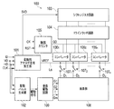
一実施の形態について図面を参照して説明する。図1Aは一実施の形態の画像表示装置を示すブロック図、図1Bは画素の一例を示す構成図である。 An embodiment will be described with reference to the drawings. FIG. 1A is a block diagram illustrating an image display device according to an embodiment, and FIG. 1B is a configuration diagram illustrating an example of a pixel.
本実施の形態の画像表示装置100は、反射型液晶プロジェクタなどに用いる液晶表示装置である。
The
画像表示装置100は、変換用アナログ信号発生部101、駆動パルス生成部102、シフトレジスタ回路103、1ラインラッチ回路104、階調カウンタ105、コンパレータ1061〜106n、アナログスイッチ1071〜107n、画素部108、垂直駆動回路109を備える。The
変換用アナログ信号発生部101には、表示すべきデジタル映像信号ID、垂直同期信号VD、水平同期信号HD、クロックCLKが入力される。
A digital video signal ID to be displayed, a vertical synchronization signal VD, a horizontal synchronization signal HD, and a clock CLK are input to the conversion analog
変換用アナログ信号発生部101は、後述する所定の処理を施して、互いに同期した表示用デジタル映像信号SVDとランプ信号VREFとを発生する。
The conversion analog
表示用デジタル映像信号SVDはシフトレジスタ回路103に供給され、ランプ信号VREFはランプ信号線Lsを介してアナログスイッチ1071〜107nの入力端子に供給される。The display digital video signal SVD is supplied to the
ランプ信号VREFは、黒レベル及び白レベルのうち一方のレベルから開始して1水平走査期間の終了時点直前には他方のレベルに達するように1水平走査期間周期でレベルが漸次変化する傾斜波である。 The ramp signal VREF is a ramp wave whose level gradually changes in one horizontal scanning period so that it starts from one of the black level and white level and reaches the other level immediately before the end of one horizontal scanning period. is there.
駆動パルス生成部102には、垂直同期信号VD、水平同期信号HD、クロックCLKが入力される。駆動パルス生成部102は、表示用デジタル映像信号SVDとランプ信号VREFとに同期した駆動信号を生成し、垂直駆動回路109に供給する。
The drive
シフトレジスタ回路103は、供給される表示用デジタル映像信号SVDを画素単位で順次シフトする。1ラインラッチ回路104は、シフトレジスタ回路103から並列に出力されるデジタル映像信号(以下、画素データともいう)を、1ライン単位で一時保持する。
The
シフトレジスタ回路103及び1ラインラッチ回路104は、表示用デジタル映像信号SVDにおける1ライン分の各画素の画像データを保持する保持部を構成している。
The
階調カウンタ105は、デジタル映像信号IDの同期信号に同期した所定周波数のクロックCKをカウントし、1ライン周期で一巡し、かつ、表示階調の最小値から最大値まで変化するカウンタ値QD(基準階調データ)を出力する。
The
n個のコンパレータ1061〜106nは、画素部108の水平方向のn個の画素ごとに対応して設けられており、階調カウンタ105のカウンタ値QDと、1ラインラッチ回路104からの1ラインのn個の画素データとを比較し、両者が一致したときに一致パルスを出力する。The n comparators 106 1 to 106 n are provided corresponding to each of n pixels in the horizontal direction of the
アナログスイッチ1071〜107nは、コンパレータ1061〜106n、及び、画素部108の水平方向のn個の画素ごとにそれぞれ対応して設けられている。アナログスイッチ1071〜107nは、水平走査期間ごとに、水平走査期間の開始時に同時にオンに制御され、ランプ信号VREFを、データ線D1〜Dnを介して、対応して設けられた、画素部108の垂直方向のm個の画素に供給する。The analog switches 107 1 to 107 n are provided corresponding to the comparators 106 1 to 106 n and n pixels in the horizontal direction of the
画素部108は、画面水平方向の画素数n個、画面垂直方向の画素数m個(すなわち、m行n列)の2次元マトリクス状に配置された画素から構成されている。
The
画素部108は、同じ垂直方向のm個の画素単位でn本のデータ線D1〜Dnに別々に接続されており、また、同じ水平方向のn個の画素単位でm本のゲート線G1〜Gmに別々に接続されている。The
すなわち、画素部108は、n本のデータ線D1〜Dnとm本のゲート線G1〜Gmとが交差する各交差部にそれぞれ設けられた、n×m個の画素からなる。That is, the
各画素としては、例えば図1Bに示す構成の画素110を用いることができる。図1Bにおいて、画素110はデータ線Dとゲート線Gとが交差する交差部に設けられた、画素選択トランジスタQ、信号保持容量Cs、液晶素子111から構成されている。
As each pixel, for example, the
データ線Dとは、図1Aのデータ線D1〜Dnのうちの任意の1本であり、ゲート線Gとは、図1Aのゲート線G1〜Gmのうちの任意の1本である。The data line D is any one of the data lines D 1 to D n in FIG. 1A, and the gate line G is any one of the gate lines G 1 to G m in FIG. 1A. is there.
画素選択トランジスタQは、ゲートがゲート線Gに接続され、ドレインがデータ線Dに接続され、ソースが信号保持容量Csの非接地側端子と液晶素子111の画素駆動電極PEとに接続されている。
The pixel selection transistor Q has a gate connected to the gate line G, a drain connected to the data line D, and a source connected to the non-ground side terminal of the signal holding capacitor Cs and the pixel drive electrode PE of the
画素110は、ゲート線Gを介して入力される画素選択信号(ゲート信号)により画素選択トランジスタQがオンされて選択される。画素110には、アナログスイッチ1071〜107nのうち対応して設けられた1個のアナログスイッチに接続されたデータ線Dを介してランプ信号が入力される。The
画素110は、アナログスイッチがオフされた時点でサンプリングされたランプ信号(すなわち、DA変換されたアナログ映像信号)を、画素選択トランジスタQを介して信号保持容量Csに書き込み保持した後、液晶素子111の画素駆動電極PEに印加するよう構成されている。
The
表示素子の一例としての液晶素子111は、互いに対向して配置された画素駆動電極PEと、共通電圧Vcomが印加される共通電極(透明電極)CEとの間に液晶層LCMが挟持された構造を有する。
A
液晶素子111は、画素駆動電極PEをアナログ映像信号電圧(ここでは、サンプリングされたランプ信号電圧)に応じた電圧で駆動することで液晶層LCMの光透過率を制御し、映像を表示する。
The
垂直駆動回路109は垂直方向駆動部を構成しており、駆動信号が入力される。垂直駆動回路109は、m本のゲート線G1〜Gmに、水平同期信号HDに同期した1水平走査期間(1H)単位で1本ずつ順次に画素選択信号を供給して、画素部108の同じ水平方向のn個の画素を同時に選択することを繰り返す。これによって、垂直駆動回路109は、1フレーム期間で全画素を選択する。The
次に、図1Aに示す画像表示装置100の概略動作について図2のタイミングチャートを参照して説明する。
Next, the schematic operation of the
変換用アナログ信号発生部101は、図2の(a)に示す水平同期信号HDに同期した、図2の(b)に示す複数ビットの画素データが時系列的に合成された表示用デジタル映像信号SVDと、図2の(i)に示す1水平走査期間周期のランプ信号VREFとを発生する。
The conversion
シフトレジスタ回路103は、入力された表示用デジタル映像信号SVDを図2の(c)に示すシフトクロックSCLKに基づいてシフトして1ライン分ずつ順次展開する。
The
1ラインラッチ回路104は、シフトレジスタ回路103で1ライン分の表示用デジタル映像信号SVDの展開が終了した時点で、シフトレジスタ回路103から並列に出力される1ライン分のn個の画素データを、図2の(d)に模式的に示すように一時保持する。1ラインラッチ回路104は、画素データを保持した後、コンパレータ1061〜106nの第1のデータ入力端子に供給する。The one-
階調カウンタ105は、図2の(e)に示すクロックCKをカウントして、図2の(f)に示すように、複数の階調値が水平走査期間内で最小値から最大値まで順次に変化するカウント値QDを水平走査期間ごとに出力する。階調カウンタ105は、カウント値QDをコンパレータ1061〜106nの第2のデータ入力端子に共通に供給する。The
コンパレータ1061〜106nは、第1のデータ入力端子に画素単位に供給される画素データと、第2のデータ入力端子に共通に供給されるカウント値QDとを互いに独立して比較し、両者が一致したときに一致パルスを出力する。The comparators 106 1 to 106 n independently compare the pixel data supplied to the first data input terminal in units of pixels and the count value QD supplied in common to the second data input terminal. A coincidence pulse is output when they match.
コンパレータ1061〜106nは、アナログスイッチ1071〜107nのうち、対応して設けられたアナログスイッチに、一致パルスを供給してオフとする。
階調カウンタ105及びコンパレータ1061〜106nは、アナログスイッチの制御部を構成している。The comparators 106 1 to 106 n supply matching pulses to the corresponding analog switches among the analog switches 107 1 to 107 n to turn them off.
The
アナログスイッチ1071〜107nには、図2の(g)に示すスイッチスタートパルスが入力され、各水平走査期間の開始時点ごとにすべて同時にオンとされる。
なお、スイッチスタートパルス、クロックCK、シフトクロックSCLK、ランプ信号VREFは、すべて水平同期信号HDに同期している。The analog switches 107 1 to 107 n receive the switch start pulse shown in FIG. 2G and are turned on simultaneously at the start of each horizontal scanning period.
Note that the switch start pulse, the clock CK, the shift clock SCLK, and the ramp signal VREF are all synchronized with the horizontal synchronization signal HD.
その後、アナログスイッチ1071〜107nは、コンパレータ1061〜106nのうち対応して設けられたコンパレータから出力された一致パルスによりオフとされる。Thereafter, the analog switches 107 1 to 107 n are turned off by the coincidence pulse output from the corresponding comparator provided among the comparators 106 1 to 106 n .
図2の(h)は、アナログスイッチ1071〜107nのうちのある1つのアナログスイッチの開閉タイミングを示しており、ハイレベルはオン期間、ローレベルはオフ期間を模式的に示している。FIG. 2H shows the opening / closing timing of one analog switch among the analog switches 107 1 to 107 n , where the high level schematically shows the on period and the low level schematically shows the off period.
すなわち、図2の(h)は、ハイレベルからローレベルに変化した時点で、当該アナログスイッチが一致パルスを受けてオフとなったことを示している。 That is, (h) in FIG. 2 indicates that the analog switch has been turned off in response to the coincidence pulse at the time of changing from the high level to the low level.
ここでは、図2の(h)に開閉タイミングが示されているアナログスイッチは、そのアナログスイッチが設けられた画素列に対応した1画素の階調値が、ある1ラインではカウント値QDがjのときにオフとされ、次の1ラインではカウント値QDがkのときにオフとされる。 Here, in the analog switch whose opening / closing timing is shown in (h) of FIG. 2, the gradation value of one pixel corresponding to the pixel column in which the analog switch is provided has a count value QD of j in one line. Is turned off when the count value QD is k in the next one line.
アナログスイッチ1071〜107nに接続されたデータ線の電位は、アナログスイッチ1071〜107nのオン期間中は入力されるランプ信号VREFに応じて徐々に高くなっていく。The potential of the data lines connected to the analog switch 107 1 to 107 n is in the ON period of the analog switches 107 1 to 107 n is gradually increased in response to the ramp signal VREF input.
アナログスイッチがオフとなった時点以降、次の水平走査期間の開始まではオフ状態が継続されるため、データ線にはアナログスイッチがオフとなる直前の図2の(i)に白丸で示すランプ信号VREFの電位がサンプリング保持される。 After the analog switch is turned off, the off state is continued until the start of the next horizontal scanning period. Therefore, the data line is indicated by a white circle in FIG. 2 (i) immediately before the analog switch is turned off. The potential of the signal VREF is sampled and held.
サンプリング保持された電位は、そのデータ線を介して接続された画素部108内の垂直方向に配列されたm個の画素のうち、そのときにゲート線G1〜Gmで選択されている1画素の信号保持容量Csに保持される。The sampled and held potential is selected by the gate lines G 1 to G m among the m pixels arranged in the vertical direction in the
このとき保持されたランプ信号VREFの電圧は、その画素のデジタル映像信号の画素値(階調レベル)に対応している。すなわち、入力された表示用デジタル映像信号SVDの画素データは、アナログ映像信号に変換されて画素の信号保持容量Csに蓄積される。 The voltage of the ramp signal VREF held at this time corresponds to the pixel value (gradation level) of the digital video signal of the pixel. That is, the input pixel data of the display digital video signal SVD is converted into an analog video signal and stored in the signal holding capacitor Cs of the pixel.
このようにして、各画素にはアナログスイッチ1071〜107nがオフになる直前の時点のランプ信号VREFの電圧が、それぞれの画素の信号保持容量Csで次のフレームまで保持されて、それぞれの画素の液晶素子が駆動される。In this way, the voltage of the ramp signal VREF at the time immediately before the analog switches 107 1 to 107 n are turned off is held in each pixel until the next frame by the signal holding capacitor Cs of each pixel. The liquid crystal element of the pixel is driven.
画像表示装置100において、アナログスイッチ1071〜107nがオフになるタイミング、すなわちランプ信号の電圧をサンプリング保持するタイミングはそのときに表示しようとする映像信号の絵柄によって異なり、すべて同時の場合もあれば互いに異なる場合もある。In the
オフになる順序も固定されているわけではない。黒レベル(液晶層の光透過率ゼロ相当)から白レベル(液晶層の光透過率100%相当)へ向かって漸次レベルが変化するランプ信号VREFを入力した場合であれば、黒側のレベルを表示しようとする画素に繋がるアナログスイッチから順にオフになる。絵柄によってその都度オフになる順番は異なる。 The order in which they are turned off is not fixed. If the ramp signal VREF whose level gradually changes from the black level (corresponding to zero light transmittance of the liquid crystal layer) to the white level (corresponding to light transmittance of 100% of the liquid crystal layer) is input, the black side level is changed. The analog switches connected to the pixels to be displayed are turned off in order. The turn-off order varies depending on the pattern.
画像表示装置100は、ランプ信号を用いたDA変換方式の動作により直線性がよいなどの特長を有する。画像表示装置100は、ダミー画素を画素内に設けることなく、表示用デジタル映像信号の各ライン単位でダイナミックに変動するランプ信号データ生成部の負荷変動に起因するランプ信号の電圧変動による階調劣化(波形妨害)を高精度に抑圧するために、変換用アナログ信号発生部101を設けている。
The
次に、変換用アナログ信号発生部101の構成及び動作について詳細に説明する。
Next, the configuration and operation of the conversion analog
図3は、変換用アナログ信号発生部101の具体的な構成例を示すブロック図、図4は、図3の概略動作説明用タイミングチャートを示す。なお、図4の(a)〜(d)と(e)〜(r)とは便宜上、時間軸を変えて図示してある。
FIG. 3 is a block diagram illustrating a specific configuration example of the conversion analog
図3に示すように、変換用アナログ信号発生部101には、表示すべきデジタル映像信号ID、垂直同期信号VD、水平同期信号HD、クロックCLKが入力される。
As shown in FIG. 3, the conversion analog
変換用アナログ信号発生部101は、奇数ラインランプ信号データ生成部201A、偶数ラインランプ信号データ生成部201B、1ビットラインカウンタ202、アドレスカウンタ203、NOT回路204、画像データセレクタ211、ヒストグラム値セレクタ212、ランプ信号データ生成部213、DA変換部214を有する。
The conversion analog
変換用アナログ信号発生部101は、表示用デジタル映像信号SVDとランプ信号VREFとを生成して出力する。
The conversion analog
奇数ラインランプ信号データ生成部201Aは、奇数1ラインデータメモリ205a(以下、データメモリ205a)、奇数ラインヒストグラムメモリ206a(以下、ヒストグラムメモリ206a)、AND回路207a、加算器208a、スイッチ209a、奇数ライン累積加算器210aを有する。
The odd line ramp signal
ヒストグラムメモリ206aは、水平走査期間ごとに、奇数ラインの1ラインの各画素の画像データが有する階調値のヒストグラム値を検出して、ヒストグラム値データを出力するヒストグラム値出力部である。
The
偶数ラインランプ信号データ生成部201Bは、奇数ラインランプ信号データ生成部201Aと同様の構成である。
The even line ramp signal
偶数ラインランプ信号データ生成部201Bは、偶数1ラインデータメモリ205b(以下、データメモリ205b)、偶数ラインヒストグラムメモリ206b(以下、ヒストグラムメモリ206b)、AND回路207b、加算器208b、スイッチ209b、偶数ライン累積加算器210bを有する。
The even line ramp signal
ヒストグラムメモリ206bは、水平走査期間ごとに、偶数ラインの1ラインの各画素の画像データが有する階調値のヒストグラム値を検出して、ヒストグラム値データを出力するヒストグラム値出力部である。
The
なお、データメモリ205a及び205b、並びに、ヒストグラムメモリ206a及び206bは、書き込みと読み出しを独立に実行できるデュアルポートメモリである。
The
ここで、奇数ラインと偶数ラインとに処理を分けるのは、ヒストグラムを生成するのに1ラインの期間が必要であり、この期間はヒストグラムが確定していないためである。 Here, the reason for dividing the processing into the odd lines and the even lines is that a period of one line is necessary to generate the histogram, and the histogram is not fixed during this period.
すなわち、奇数ライン側処理及び偶数ライン側処理のうち一方の側の処理でヒストグラム値を生成している間は、もう一方の側の処理でヒストグラム値を読み出し、これを1ラインごとに交互に切り換えるためである。 That is, while the histogram value is generated by the process on one side of the odd line side process and the even line side process, the histogram value is read by the process on the other side, and this is alternately switched for each line. Because.
データメモリ205a及び205bは、ヒストグラム生成で生じる1ライン分の時間遅延にタイミングを合わせるために用いられる。
The
1ビットラインカウンタ202には、図4の(b)に示す垂直同期信号VDと、図4の(c)及び(g)に示す水平同期信号HDとが供給される。1ビットラインカウンタ202は、図4の(a)及び(e)に示す入力デジタル映像信号の画像データIDが、奇数ライン画像データID(1),ID(3),…であるか、偶数ライン画像データID(2),ID(4),…であるかを示す判定信号LINEを生成する。
The 1-
図4の(d)及び(h)に示すように、判定信号LINEは、一例として、画像データが奇数ラインの場合“1”、偶数ラインの場合“0”とする。 As shown in FIGS. 4D and 4H, for example, the determination signal LINE is “1” when the image data is an odd line and “0” when the image data is an even line.
1ビットラインカウンタ202は、判定信号LINEをライトイネーブル信号として、データメモリ205a及びヒストグラムメモリ206aの各ライトイネーブル端子WEに供給する。
The 1-
NOT回路204は判定信号LINEを極性反転し、極性反転した信号をライトイネーブル信号としてデータメモリ205b及びヒストグラムメモリ206bの各ライトイネーブル端子WEに供給する。
The
AND回路207aは、判定信号LINEと水平同期信号HDとを論理積演算して、ヒストグラムメモリ206a及び奇数ライン累積加算器210aの各クリア端子CLRにクリア信号としてそれぞれ供給する。
The AND
AND回路207bは、NOT回路204で判定信号LINEを極性反転した信号と水平同期信号HDとを論理積演算して、ヒストグラムメモリ206b及び偶数ライン累積加算器210bの各クリア端子CLRにクリア信号としてそれぞれ供給する。
The AND circuit 207b performs an AND operation on the signal obtained by inverting the polarity of the determination signal LINE in the
アドレスカウンタ203は、水平同期信号HDと図4の(f)に示すクロックCLKとから画像データIDに同期した、図4の(i)に模式的に示すカウンタ値ACを生成する。
The
アドレスカウンタ203は、カウンタ値ACをデータメモリ205a及び205bの各書き込みアドレス端子WADRSと読み出しアドレス端子RADRSにそれぞれ供給する。
The
データメモリ205a及び205bは、ライトイネーブル信号が“1”のとき、端子WDATAに入力される画像データIDを書き込み、ライトイネーブル信号が“0”のとき、書き込まれている画像データを端子RDATAから読み出す。
The
データメモリ205a及び205bには、前述したように互いに逆極性で、奇数ラインのとき“1”、偶数ラインのとき“0”であるライトイネーブル信号が供給される。
As described above, the
よって、データメモリ205aは、奇数1ラインの画像データを書き込み、その奇数1ラインの画像データを、図4の(j)に模式的に示すように、次の偶数1ライン入力期間に読み出す。
Therefore, the
データメモリ205bは偶数1ラインの画像データを書き込み、その偶数ラインの画像データを、図4の(n)に模式的に示すように、次の奇数1ライン入力期間に読み出す。
The
画像データセレクタ211は、セレクト端子SELに供給される判定信号LINEが“0”のとき、端子Aに供給されているデータメモリ205aから読み出された奇数1ラインの画像データID_ODDを選択して出力する。
When the determination signal LINE supplied to the select terminal SEL is “0”, the
画像データセレクタ211は、判定信号LINEが“1”のとき、端子Bに供給されているデータメモリ205bから読み出された偶数1ラインの画像データID_EVENを選択して出力する。
When the determination signal LINE is “1”, the
これにより、画像データセレクタ211は、図4の(q)に模式的に示すように、入力画像データIDの奇数1ライン入力期間は偶数1ラインの画像データを選択し、偶数1ライン入力期間は奇数1ラインの画像データを選択する。
As a result, the
画像データセレクタ211は、選択した画像データを、表示用デジタル映像信号SVDとして、図1Aのシフトレジスタ回路103に供給する。
The
データメモリ205a及び205bと画像データセレクタ211からなる構成は1ライン遅延回路(遅延部)であって、奇数ラインと偶数ラインを選択的に出力する機能を有する。
The configuration including the
データメモリ205a及び205bと画像データセレクタ211よりなる遅延部は、DA変換部214から出力されるランプ信号VREFに同期して、1ラインの各画素の画像データを遅延して、シフトレジスタ回路103及び1ラインラッチ回路104よりなる保持部に供給する。
A delay unit including the
ヒストグラムメモリ206aは、データメモリ205aが奇数1ラインの画像データの書き込み中の期間、1ライン分のヒストグラムを書き込む。ヒストグラムメモリ206bは、データメモリ205bが偶数1ラインの画像データ書き込み中の期間、1ライン分のヒストグラムを書き込む。
The
加算器208a,208bは、ヒストグラムメモリ206a,206bの端子RDATAより出力された読み出しデータに“1”を加算して、端子WDATAに供給する。
The
つまり、ヒストグラムメモリ206a及び206bは、入力画像データIDが書き込みアドレス端子WADRSに供給され、加算器208a,208bがヒストグラムメモリ206a,206bからの読み出しデータに“1”を加算した値をヒストグラムメモリ206a及び206bに書き込むことでヒストグラム値を生成する。
That is, in the
ヒストグラムメモリ206a,206bからの読み出しデータは、書き込みアドレス端子WADRSに供給された入力画像データIDの画素の階調に対応したアドレスに記憶されていた値である。
The read data from the
ヒストグラムメモリ206a及び206bは、クリア信号により1ライン書き込み開始前に、以前記憶した別ラインのヒストグラム値がすべてクリアされる。
In the
ヒストグラムメモリ206a及び206bの読み出しアドレス端子RADRSには、スイッチ209a,209bを介して互いに逆論理値の読み出しアドレス信号が供給され、書き込みを行わない各ラインで読み出し動作が行われる。
The read address terminals RADRS of the
奇数ライン累積加算器210aは、AND回路207aからの1水平走査期間(1H)周期の信号によりクリアされた後、ヒストグラムメモリ206aの端子RDATAから1H内で順次に読み出される、図4の(k)に模式的に示す奇数ラインの複数のヒストグラム値HISTD_ODDを累積加算する。
The
奇数ライン累積加算器210aは、図4の(m)に模式的に示すように、算出した累積加算値HISTADD_ODDを出力する。
The odd line
偶数ライン累積加算器210bは、AND回路207bからの1H周期の信号によりクリアされた後、ヒストグラムメモリ206bの端子RDATAから1H内で順次に読み出される、図4の(o)に模式的に示す偶数ラインの複数のヒストグラム値HISTD_EVENを累積加算する。
The
偶数ライン累積加算器210bは、図4の(p)に模式的に示すように、算出した累積加算値HISTADD_EVENを出力する。
The even line
ヒストグラム値セレクタ212は、セレクト端子SELに供給される判定信号LINEが“0”のとき、端子Aに供給されている奇数ライン累積加算器210aから読み出された図4の(m)に示す奇数ラインの累積加算値HISTADD_ODDを選択して出力する。
When the determination signal LINE supplied to the select terminal SEL is “0”, the
ヒストグラム値セレクタ212は、判定信号LINEが“1”のとき、端子Bに供給されている偶数ライン累積加算器210bから読み出された図4の(p)に示す偶数ラインの累積加算値HISTADD_EVENを選択して出力する。
When the determination signal LINE is “1”, the
これにより、ヒストグラム値セレクタ212は、図4の(r)に模式的に示すように、画像データセレクタ211から出力されている1ラインの画像データと同じラインのヒストグラム値を示すヒストグラム値データHISTDを出力する。
As a result, the
なお、図4の(r)において、HISTD(1)で示すa1,b1,c1,d1,…は、奇数ライン画像データID(1)の各階調の出現頻度(ヒストグラム値)である。HISTD(2)で示すa2,b2,c2,d2,…は、偶数ライン画像データID(2)の各階調の出現頻度(ヒストグラム値)である。 In FIG. 4 (r), a1, b1, c1, d1,... Indicated by HISTD (1) are appearance frequencies (histogram values) of each gradation of the odd line image data ID (1). A2, b2, c2, d2,... Indicated by HISTD (2) are the appearance frequencies (histogram values) of each gradation of the even line image data ID (2).
次に、ヒストグラムメモリ206a及び206b、奇数ライン累積加算器210a及び偶数ライン累積加算器210bの動作を、図5のタイミングチャートを参照してさらに詳細に説明する。
Next, the operations of the
図5の(a)に示す入力画像データIDは、垂直同期信号(垂直リセット信号)VD、図5の(c)に示す水平同期信号(水平リセット信号)HD、及び、図5の(b)に示すクロックCLKに同期している。 The input image data ID shown in (a) of FIG. 5 includes a vertical synchronization signal (vertical reset signal) VD, a horizontal synchronization signal (horizontal reset signal) HD shown in (c) of FIG. 5, and (b) of FIG. Is synchronized with the clock CLK shown in FIG.
図5の(d)は、図3の1ビットラインカウンタ202より出力される判定信号LINEを示している。ここでは、判定信号LINEは、入力画像データIDが奇数ラインの画像データID(11)のとき“1”、偶数ラインの画像データID(12)のとき“0”である。
FIG. 5D shows the determination signal LINE output from the 1-
アドレスカウンタ203は、図5の(e)に示すように、一例として、1H期間内で“0”から“7”まで1ずつカウントアップしてカウンタ値ACを出力する。アドレスカウンタ203は、1Hごとにカウントアップを繰り返す。ここでは、説明を簡単にするため、1H期間の画像データ数(水平画素数)を“8”としている。
As shown in FIG. 5E, for example, the
判定信号LINEが“1”である奇数ラインの画像データ入力期間では、ヒストグラムメモリ206aは奇数ラインのヒストグラムを生成する。
In the image data input period of odd lines where the determination signal LINE is “1”, the
この期間では、ヒストグラムメモリ206aの書き込みイネーブル端子WEには、図5の(h)に示すように、判定信号LINE“1”がライトイネーブル信号として入力される。
During this period, as shown in FIG. 5H, the determination signal LINE “1” is input to the write enable terminal WE of the
ヒストグラムメモリ206aの読み出しアドレス端子RADRSには、端子“1”側に接続されたスイッチ209aを介して、図5の(j)に模式的に示すように、図5の(a)に示す奇数ラインの入力画像データID(11)が入力される。
The read address terminal RADRS of the
ヒストグラムメモリ206aの書き込みアドレス端子WADRSには、図5の(i)に模式的に示す入力画像データID(11)の画素値が書き込みアドレスとして入力される。ヒストグラムメモリ206aは、入力画像データID(11)の画素値を書き込みアドレスとして、端子WDATAに供給される図5の(m)に模式的に示す加算器208aからのデータを書き込む。
The pixel value of the input image data ID (11) schematically shown in (i) of FIG. 5 is input as a write address to the write address terminal WADRS of the
ヒストグラムメモリ206aの端子RDATAから読み出されるデータは、図5の(k)に示すように、データが読み出される以前に、書き込みアドレス端子WADRSに入力されたその書き込みアドレスが選択された回数を示す。
The data read from the terminal RDATA of the
よって、ヒストグラムメモリ206aに書き込まれる書き込みデータは、端子RDATAから読み出された、書き込みアドレスが選択された回数を示すデータに加算器208aで“1”を加算した値のデータである。
Therefore, the write data written to the
すなわち、入力画像データID(11)の1ラインの8つの画素が、例えば図5の(a)に示すように、2,5,3,2,7,2,5,3の各画素値(階調)で順番に入力されるとき、ヒストグラムメモリ206aは、それぞれの階調を示すアドレスを書き込みアドレス及び読み出しアドレスとして選択する。
That is, eight pixels in one line of the input image data ID (11) are represented by pixel values (2, 5, 3, 2, 7, 2, 5, 3) as shown in FIG. The
ヒストグラムメモリ206aは、選択した書き込みアドレス及び読み出しアドレスの回数に“1”を加算した値を書き込む。
The
ヒストグラムメモリ206aのクリア端子CLRには、AND回路207aより水平同期信号HDがクリア信号として入力される。
The horizontal synchronization signal HD is input as a clear signal from the AND
ヒストグラムメモリ206aに書き込まれたアドレス0〜7の書き込みデータ値(ヒストグラム値)は、クリア信号によって、図5の(g)に示すように、水平同期信号HDの立ち上がりエッジですべて0にクリアされる。
The write data values (histogram values) written in the
従って、ヒストグラムメモリ206aにおけるアドレス0〜7の書き込みデータ値は、最初はすべて“0”である。
Accordingly, all the write data values at
図5の(k)に示すように、最初から3つの入力画素値に対応した読み出しアドレス2,5,3からはデータ値“0”が読み出される。 As shown in FIG. 5 (k), the data value “0” is read from the read addresses 2, 5, and 3 corresponding to the three input pixel values from the beginning.
図5の(m)に示すように、アドレス2,5,3のデータ値“0”に“1”が加算されて、ヒストグラムメモリ206aには、アドレス2,5,3のデータ値“1”がそれぞれ書き込まれる。
As shown in FIG. 5 (m), “1” is added to the data value “0” at
続く4番目の画素値に対応した読み出しアドレス2からは以前に書き込まれた“1”が読み出され、それに“1”を加算して“2”がアドレス2に上書きされる。
The previously written “1” is read from the read
以下、同様にして、1ラインの画素入力後には図5の(n)に示すように、アドレス2の書き込みデータ値が“3”、アドレス3,5の各書き込みデータ値が“2”、アドレス7の書き込みデータ値が“1”で、それ以外のアドレス0,1,4,6は“0”となる。
Similarly, after one line of pixels is input, the write data value at
つまり、ヒストグラムメモリ206aには、階調値をアドレスとし、アドレスに書き込まれたデータ値を階調の累計値とする、奇数ラインの8つの画素の階調ごとの累計値であるヒストグラム値HISTD_Qが記憶されることになる。
That is, in the
このようにして、ヒストグラムメモリ206aは、判定信号LINEが“1”であるとき、奇数ラインの入力画像データの各階調のヒストグラム値HISTD_ODDを生成する。
In this way, when the determination signal LINE is “1”, the
続いて、判定信号LINEが“0”である偶数ラインの画像データ入力期間では、ヒストグラムメモリ206aの上記の動作と同様の動作により、ヒストグラムメモリ206bは偶数ラインの入力画像データの各階調のヒストグラム値HISTD_EVENを生成する。
Subsequently, in the image data input period for even-numbered lines in which the determination signal LINE is “0”, the
これと同時に、ヒストグラムメモリ206aは、“1”のライトイネーブル信号が供給されないので読み出し動作のみを行い、直前の奇数ラインの画像データ入力期間に記憶したヒストグラム値HISTD_ODDを用いて負荷変動を補正する。
At the same time, since the “1” write enable signal is not supplied, the
偶数ラインの画像データ入力期間では、スイッチ209aが端子“0”側に切り換え接続される。よって、ヒストグラムメモリ206aの端子RADRSには、図5の(j)及び(f)に示すように、図5の(e)に示すカウンタ値ACがスイッチ209aを介して読み出しアドレスとして供給される。
In the even line image data input period, the
これにより、ヒストグラムメモリ206aは、水平同期信号をリセットとし、1ずつインクリメントするカウンタ値ACの値を読み出しアドレスとする。ヒストグラムメモリ206aは、図5の(n)に示す奇数ラインの画像データ入力期間に記憶したヒストグラム値HISTD_ODDを、図5の(k)に示すように順次に出力する。
As a result, the
ヒストグラム値HISTD_ODDは、アドレス2から読み出される階調値“2”が3、アドレス3,5からそれぞれ読み出される階調値“3”,“5”がそれぞれ2、アドレス7から読み出される階調値“7”が1で、それ以外の階調値“0”,“1”,“4”,“6”は0である。
The histogram value HISTD_ODD has the gradation value “2” read from the
なお、ヒストグラム値は1ライン遅延しており、この期間に対応した奇数ラインの画像データも、データメモリ205aから1ライン遅延されてID_ODDとして出力される。
Note that the histogram value is delayed by one line, and the image data of odd lines corresponding to this period is also delayed by one line from the
奇数ライン累積加算器210aの端子INDATAには、ヒストグラムメモリ206aから読み出された図5の(k)に示す奇数ラインの階調のヒストグラム値HISTD_ODDが入力される。奇数ライン累積加算器210aは、ヒストグラム値HISTD_ODDを累積加算し、図5の(o)に示す累積加算値HISTADD_ODDを端子EXDATAから出力する。
The histogram value HISTD_ODD of the gradation of the odd line shown in FIG. 5 (k) read from the
この累積加算値HISTADD_ODDは、その時点でオフされているアナログスイッチの数sを示している。 This cumulative addition value HISTADD_ODD indicates the number s of analog switches that are turned off at that time.
以上説明した奇数ラインの画像データ入力期間における入力画像データID(11)の階調(データレベル)と、ヒストグラム値HISTD_ODDと、累積加算値HISTADD_ODDとをまとめると図6に示すとおりとなる。 The gradation (data level) of the input image data ID (11), the histogram value HISTD_ODD, and the cumulative addition value HISTADD_ODD in the image data input period of the odd-numbered lines described above are summarized as shown in FIG.
偶数ラインの画像データ入力期間においては、偶数ラインランプ信号データ生成部201Bによって、奇数ラインの画像データ入力期間と同様の動作が行われる。このときの動作は1H期間奇数ラインの動作とずれているだけであり、その動作は容易に類推できるのでその詳細な説明は省略する。
In the even line image data input period, the even line ramp signal
ヒストグラムメモリ206bは、偶数ラインのヒストグラム値HISTD_EVENを出力し、偶数ライン累積加算器210bは偶数ラインのオフされているアナログスイッチ数sを示す累積加算値HISTADD_EVENを出力する。
The
ヒストグラムメモリ206a及び206bは、ランプ信号を1H期間内で最も低い階調レベルから最も高い階調レベル方向へ波形を変化させる場合は、最も低い階調0のヒストグラム値から最も高い階調のヒストグラム値の方向の順で水平同期信号に同期して出力する。
The
逆に、ヒストグラムメモリ206a及び206bは、ランプ信号を1H期間内で最も高い階調レベルから最も低い階調レベル方向へ波形を変化させる場合は、最も高い階調のヒストグラム値から最も低い階調のヒストグラム値の方向の順で水平同期信号に同期して出力する。
以下の説明ではランプ信号の波形は前者の場合であるとする。Conversely, when changing the waveform of the ramp signal from the highest gradation level to the lowest gradation level in the 1H period, the
In the following description, the waveform of the ramp signal is assumed to be the former case.
図3に示すヒストグラム値セレクタ212は、セレクト端子SELに供給される判定信号LINEが“0”のとき、図5の(p)に模式的に示すように、端子Aに供給されている奇数ライン累積加算器210aから出力された奇数ラインの累積加算値HISTADD_ODDを選択してヒストグラム値データHISTDとして出力する。
When the determination signal LINE supplied to the select terminal SEL is “0”, the
この期間では、画像データセレクタ211からは、図5の(q)に模式的に示すように、同じ奇数ラインの画像データID_ODDが出力される。
During this period, the
また、ヒストグラム値セレクタ212は、セレクト端子SELに供給される判定信号LINEが“1”のとき、端子Bに供給されている偶数ライン累積加算器210bから出力された偶数1ラインの累積加算値HISTADD_EVENを選択してヒストグラム値データHISTDとして出力する。
Further, the
図3に示すランプ信号データ生成部213には、ヒストグラム値セレクタ212から選択されて出力されたヒストグラム値データHISTDと、クロックCLKと、水平同期信号HDとが供給される。
The ramp signal
ランプ信号データ生成部213は、1H期間の最初で最小の階調値から開始して1H期間の終了直前で最大の階調値を示す傾斜波であり、かつ、その傾斜の程度が累積加算値に応じて可変制御された非線形の傾斜を示すデジタル値のランプ信号データVREFDを生成する。
The ramp signal
DA変換部214は、バッファを内蔵しており、デジタル信号であるランプ信号データVREFDをクロックCLKに基づきアナログ信号のランプ信号VREFに変換する。DA変換部214は、図1Aに示すランプ信号線Ls介して、ランプ信号VREFをアナログスイッチ1071〜107nにそれぞれ供給する。The
ランプ信号データ生成部213は、傾斜の程度が累積加算値に応じて可変制御された非線形の傾斜を示すデジタル値のランプ信号データVREFDを生成する。よって、変換用アナログ信号発生部101は、DA変換部214の出力インピーダンスと、アナログスイッチ1071〜107nを代表とする入力インピーダンスとでダイナミックに生じる負荷変動に起因するランプ信号の電圧変動を抑圧する。The ramp signal
ランプ信号の電圧変動の抑圧について具体的に説明する。DA変換部214及びアナログスイッチ1071〜107nからなる回路部の等価回路は従来と同様に図16で表される。ここで、図3に示すDA変換部214内のバッファの出力インピーダンスをZ0、図1Aに示すアナログスイッチ1071〜107n1個当たりの入力インピーダンスをZ1とし、入力された階調を表示するためにオフされるアナログスイッチの数をsとすると、負荷変動率は次式で表される。
負荷変動率=V1(s)/V0=Z1/{(n−s)Z0+Z1} …(2)The suppression of the voltage fluctuation of the ramp signal will be specifically described. An equivalent circuit of a circuit unit including the
Load fluctuation rate = V 1 (s) / V 0 = Z 1 / {(ns) Z 0 + Z 1 } (2)
式(2)において、0≦s≦nであり、V0はDA変換部214内のバッファの出力電圧、V1(s)はDA変換部214からランプ信号線Lsを介してn個のアナログスイッチへ供給されるランプ信号電圧である。In Equation (2), 0 ≦ s ≦ n, V 0 is the output voltage of the buffer in the
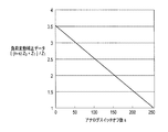
図7は、負荷変動率とアナログスイッチオフ数sとの関係の一例のグラフを示す。Z0=1、Z1=100、アナログスイッチの総数n=256とした場合、式(2)の負荷変動率は、図7に示すように、アナログスイッチオフ数sに応じて非線形的に変化する。FIG. 7 shows a graph of an example of the relationship between the load fluctuation rate and the analog switch-off number s. When Z 0 = 1, Z 1 = 100, and the total number of analog switches n = 256, the load fluctuation rate of Equation (2) changes nonlinearly according to the number of analog switch offs s as shown in FIG. To do.
負荷変動率はアナログスイッチオフ数sが少なくなるほど小さくなる。なお、上記のパラメータは視覚的に分かりやすいように設定したもので、実際のパラメータとは異なる場合がある。 The load fluctuation rate decreases as the analog switch-off number s decreases. The above parameters are set so as to be easily understood visually, and may differ from actual parameters.
図7に示す負荷変動率は、アナログスイッチオフ数sに対して非線形に変化するものであることを示している。 The load variation rate shown in FIG. 7 indicates that it changes non-linearly with respect to the analog switch-off number s.
画像表示装置100におけるランプ信号データ生成部213は、ヒストグラムメモリ206a,206bから得られる各階調の対象画素数(ヒストグラム値)の累計加算値が示すアナログスイッチオフ数sに応じて、負荷変動率に対応した図8に示す負荷変動補正データを乗じたランプ信号データVREFDを生成する。
The ramp signal
ランプ信号データVREFDは、アナログ波形としたときのランプ信号VREFがヒストグラム値に応じて可変制御されて非線形の傾斜を示す、デジタルデータである。 The ramp signal data VREFD is digital data in which the ramp signal VREF having an analog waveform is variably controlled according to the histogram value to indicate a non-linear slope.
図8に示す負荷変動補正データは、例えば式(3)によって求められる。
負荷変動補正データ={(n−s)Z0+Z1}/Z1 …(3)
負荷変動補正データは、式(2)に示す負荷変動率の逆数で求められる。負荷変動補正データは、負荷変動に基づく補正を行うことができるデータ値であればよく、式(3)に限定されない。The load fluctuation correction data shown in FIG. 8 is obtained by, for example, the equation (3).
Load fluctuation correction data = {(ns) Z 0 + Z 1 } / Z 1 (3)
The load fluctuation correction data is obtained by the reciprocal of the load fluctuation rate shown in Expression (2). The load fluctuation correction data may be any data value that can be corrected based on the load fluctuation, and is not limited to Expression (3).
以上の動作によって、本実施形態の画像表示装置100によれば、表示用デジタル映像信号のそれぞれのラインで、各階調の画像数に応じてダイナミックに変化するランプ信号データ生成部213の負荷変動に起因するランプ信号VREFの電圧変動による階調劣化を抑圧することができる。
With the above operation, according to the
次に、ランプ信号データ生成部213における負荷変動を補正したランプ信号データVREFDの生成動作について、図9,図10A〜図10B,図11A〜図11Bを参照して、さらに具体的かつ詳細に説明する。
Next, the generation operation of the ramp signal data VREFD in which the load variation is corrected in the ramp signal
画像表示装置100は、図9に示すように、黒背景であるイメージ1c上に50%グレー階調の水平画素数64画素のボックス(イメージ2c)と50%グレー階調の水平画素数128画素のボックス(イメージ3c)とが上下に隣接配置された画像を表示するものとする。なお、水平方向の全画素数nは256であるものとする。
As shown in FIG. 9, the
図9においても、50%グレー階調であるイメージ2a及び3aを白で表現している。図9に示す画像は、図15Aに示す元画像と同一の画像である。
Also in FIG. 9, the
図10A,図10B,図10Cは、それぞれ、イメージ1c,2c,3cにおける負荷変動率Fを、カウンタ値QDと入力電圧V1との関係によって示している。図11A,図11B,図11Cは、それぞれ、イメージ1c,2c,3cにおけるランプ信号データVREFDの傾斜の状態を、カウンタ値QDと入力電圧V1との関係によって示している。10A, 10B, 10C, respectively,
図10A〜図10C及び図11A〜図11Cの横軸に示すカウンタ値QDは、図1Aの階調カウンタ105より出力され、水平画素数256に対応して値“0”から“255”まで1H内でクロック周期に同期して1ずつ増加する。
The counter value QD shown on the horizontal axis of FIGS. 10A to 10C and FIGS. 11A to 11C is output from the
ランプ信号データ生成部213は、負荷変動補正を行わない場合は、1H内で、最小階調値の黒レベル(液晶層の光透過率ゼロ相当)を示す0Vから最大階調値の白レベル(液晶層の光透過率100%相当)を示す1Vまで時間の経過と共に直線的に変化する傾斜を有する1H周期の三角波であるランプ信号を発生する。
式(2)及び式(3)において、Z0=1、Z1=100とする。When the load fluctuation correction is not performed, the ramp signal
In the expressions (2) and (3), Z 0 = 1 and Z 1 = 100 are set.
黒背景であるイメージ1cの1ライン表示時には、水平方向のすべての256画素が階調値“0”であるので、カウンタ値QDが“0”のとき全水平画素に対応した256個のアナログスイッチがすべて同時にオフとなる。
At the time of displaying one line of the
このため、その後、カウンタ値QDが“255”まで変化する1H期間、256個のアナログスイッチはオフ状態を継続する。このときの負荷変動率F(255)は図10Aに示すように“1”となる(負荷変動なし)。 Therefore, thereafter, the 256 analog switches continue to be in the OFF state during the 1H period in which the counter value QD changes to “255”. The load fluctuation rate F (255) at this time is “1” as shown in FIG. 10A (no load fluctuation).
ここで、負荷変動率F(255)は100/{(256-256)×1+100}で表される。このイメージ1cの1ライン表示時には、負荷変動がないので、ランプ信号データ生成部213は図11Aに示すように0Vから1Vまでカウンタ値QDの値の変化に応じて直線的に増加する傾斜を有する三角波のランプ信号データVREFDを生成する。
Here, the load fluctuation rate F (255) is represented by 100 / {(256−256) × 1 + 100}. At the time of displaying one line of the
次に、水平幅が短い方の50%グレー階調のイメージ2cの1ライン表示時には、1ラインの256画素のうち50%グレー階調の画素が64画素、残りの黒背景の階調の画素が192画素である。
Next, when one line of the 50%
このため、水平走査期間開始直後のカウンタ値QDが“0”のとき黒背景の階調の192画素に対応した192個のアナログスイッチが同時にオフとなり、残りの64画素に対応した64個のアナログスイッチはオンとされている。 Therefore, when the counter value QD immediately after the start of the horizontal scanning period is “0”, 192 analog switches corresponding to 192 pixels of the black background gradation are simultaneously turned off, and 64 analogs corresponding to the remaining 64 pixels are turned off. The switch is turned on.
その後、50%の階調値を示すカウンタ値QDが“128”となると、50%の画素値とカウンタ値とが一致する。すると、コンパレータ1061〜106nから出力される一致パルスにより残りの64個のアナログスイッチがオフとされ、オフ直前のランプ信号(三角波)の50%階調値を示す0.5Vがサンプリングされる。この時点で256個すべてのアナログスイッチがオフとなる。Thereafter, when the counter value QD indicating the gradation value of 50% becomes “128”, the pixel value of 50% matches the counter value. Then, the remaining 64 analog switches are turned off by the coincidence pulses output from the comparators 106 1 to 106 n, and 0.5 V indicating the 50% gradation value of the ramp signal (triangular wave) immediately before the off is sampled. . At this point, all 256 analog switches are turned off.
従って、イメージ2c表示時には図10Bに示すように、カウンタ値QDが“0”〜“127”の期間の負荷変動率F(192)は式(2)より0.610(=100/{(256-192)×1+100})となり、カウンタ値QDが“128”〜“255”では1となる。
Accordingly, when the
図10Bでは、負荷変動率Fは、カウンタ値QDが“0”〜“127”では傾き0.610、カウンタ値QDが“128”〜“255”では傾き1の非線形な直線となる。 In FIG. 10B, the load fluctuation rate F is a non-linear straight line having a slope of 0.610 when the counter value QD is “0” to “127” and a slope of 1 when the counter value QD is “128” to “255”.
そこで、ランプ信号データ生成部213は負荷変動率F(192)を補正するための負荷変動補正値Hを式(3)により生成してカウンタ値QDの値の変化に応じて図11BにIで示すように変化する傾斜を有するランプ信号データVREFDを生成する。
Therefore, the ramp signal
なお、カウンタ値QDが“128”〜“255”では負荷変動率はF(255)(=1)であるので、ランプ信号データVREFDの傾斜は図11BにIIで示すように1となる。 Since the load fluctuation rate is F (255) (= 1) when the counter value QD is “128” to “255”, the slope of the ramp signal data VREFD is 1 as indicated by II in FIG. 11B.
このように、ランプ信号データ生成部213は、図11Bに示す非線形の傾斜を有するランプ信号データVREFDを生成する。
In this way, the ramp signal
次に、水平幅が長い方の50%グレー階調のイメージ3cの1ライン表示時には、1ラインの256画素のうち50%グレー階調の画素が128画素、残りの黒背景の階調の画素が128画素である。
Next, at the time of displaying one line of the 50%
このため、水平走査期間開始直後のカウンタ値QDが“0”のとき黒背景の階調の128画素に対応した128個のアナログスイッチが同時にオフとなり、残りの128画素に対応した128個のアナログスイッチはオンとされている。 For this reason, when the counter value QD immediately after the start of the horizontal scanning period is “0”, the 128 analog switches corresponding to the 128 pixels of the black background gradation are simultaneously turned off, and the 128 analog switches corresponding to the remaining 128 pixels are turned off. The switch is turned on.
その後、50%の階調値を示すカウンタ値QDが“128”となると、50%の画素値とカウンタ値とが一致する。すると、コンパレータ1061〜106nから出力される一致パルスにより残りの128個のアナログスイッチがオフとされ、オフ直前のランプ信号(三角波)の50%階調値を示す0.5Vがサンプリングされる。この時点で256個すべてのアナログスイッチがオフとなる。Thereafter, when the counter value QD indicating the gradation value of 50% becomes “128”, the pixel value of 50% matches the counter value. Then, the remaining 128 analog switches are turned off by the coincidence pulses output from the comparators 106 1 to 106 n, and 0.5 V indicating the 50% gradation value of the ramp signal (triangular wave) immediately before the off is sampled. . At this point, all 256 analog switches are turned off.
従って、イメージ3c表示時には図10Cに示すように、カウンタ値QDが“0”〜“127”の期間の負荷変動率F(128)は式(2)より0.439(=100/{(256-128)×1+100})となり、カウンタ値QDが“128”〜“255”では1となる。
Therefore, when the
図10Cでは、負荷変動率Fは、カウンタ値QDが“0”〜“127”では傾き0.439、カウンタ値QDが“128”〜“255”では傾き1の非線形な直線となる。 In FIG. 10C, the load fluctuation rate F is a non-linear straight line having a slope of 0.439 when the counter value QD is “0” to “127” and a slope of 1 when the counter value QD is “128” to “255”.
そこで、ランプ信号データ生成部213は負荷変動率F(128)を補正するための負荷変動補正値Hを式(3)により生成してカウンタ値QDの値の変化に応じて図11CにIIIで示すように変化する傾斜を有するランプ信号データVREFDを生成する。
Therefore, the ramp signal
なお、カウンタ値QDが“128”〜“255”では負荷変動率はF(255)(=1)であるので、ランプ信号データVREFDの傾斜は図11CにIVで示すように1となる。 Since the load fluctuation rate is F (255) (= 1) when the counter value QD is “128” to “255”, the slope of the ramp signal data VREFD is 1 as indicated by IV in FIG. 11C.
このように、ランプ信号データ生成部213は、図11Cに示す非線形の傾斜を有するランプ信号データVREFDを生成する。図11BのIで示す部分の傾斜と図11CのIIIで示す部分の傾斜とは、傾斜の程度が異なる。
In this way, the ramp signal
本実施の形態では、負荷変動補正を行ってランプ信号データVREFDに基づくランプ信号を生成している。よって、ランプ信号VREFをサンプルホールドして得られるイメージ2c,3cの表示画像は、従来の図15Bの表示画像におけるイメージ2b,3bと比較して、階調劣化が抑えられて本来の50%グレー階調に近い階調表示が可能になる。
In the present embodiment, load fluctuation correction is performed to generate a ramp signal based on the ramp signal data VREFD. Therefore, the display images of the
次に、図3中のランプ信号データ生成部213の具体的な構成例について説明する。
Next, a specific configuration example of the ramp signal
(ランプ信号生成部の第1構成例)
図12は、ランプ信号データ生成部213の第1構成例のブロック図を示す。図12に示す第1構成例のランプ信号データ生成部213Aは、カウンタ301及びデータ生成器302から構成される。カウンタ301は、クロックCLKをカウントアップまたはカウントダウンし、水平同期信号HDによりリセットされることで、1水平走査期間内で最小階調から最大階調までを示すカウンタ値を生成する。(First configuration example of the ramp signal generation unit)
FIG. 12 is a block diagram of a first configuration example of the ramp signal
クロックCLKは図2の(e)、図4の(f)に示すクロックであり、カウンタ301は、図1Aの階調カウンタ105が出力するカウンタ値QD(第1のカウンタ値)と同期するカウンタ値QD(第2のカウンタ値)を出力する。
The clock CLK is the clock shown in FIGS. 2E and 4F, and the
データ生成器302には、図3のヒストグラム値セレクタ212から出力されたヒストグラム値データHISTDと、カウンタ301のカウンタ値QDとがアドレスとして入力される。データ生成器302は、ヒストグラム値データHISTDとカウンタ値QDとに対応したデジタル信号であるランプ信号データVREFDを出力する。
The
データ生成器302は、ルックアップテーブル(LUT)により構成することができる。アドレスとして入力されるヒストグラム値データHISTDは、カウンタ値QDの値ごとにその時点のアナログスイッチオフ数sを示している。よって、データ生成器302は、負荷変動補正した傾斜特性の三角波のランプ信号データVREFDを生成することができる。
The
データ生成器302は、カウンタ値QDが示す三角波の補正、表示用デジタル映像信号のデガンマの実施、液晶素子の電圧−透過率特性(VT特性)の補正のうちの少なくとも1つの特性を付加したランプ信号データ(LUTデータ)を記憶している。
The
データ生成器302は、生成したランプ信号データVREFDを図3のDA変換部214に供給する。
The
図7に示した負荷変動率特性が特に非線形であり、負荷変動率が急峻に立ち上がると、表示画像には階調の段差が視認される。第1構成例のランプ信号データ生成部213Aは、階調の段差が視認される程度が許容できない場合に用いるのに好適である。
The load variation rate characteristics shown in FIG. 7 are particularly nonlinear, and when the load variation rate rises steeply, a gradation step is visually recognized in the display image. The ramp signal
また、第1構成例のランプ信号データ生成部213Aは、階調データが単調増加関数のうちの単なる三角波ではなく、表示用デジタル映像信号のデガンマも実施する非線形性を持たせる場合や、液晶素子のVT特性を一挙にまとめて補正する場合に最適な構成である。
Further, the ramp signal
アナログスイッチ1071〜107nのインピーダンスがばらつき、ヒストグラム値とは非線形のバッファ負荷となった場合でも、第1構成例のランプ信号データ生成部213Aは、アナログスイッチ1071〜107nの負荷特性に合わせたLUTデータとすることで、種々のケースに対応できる。Even when the impedance of the analog switches 107 1 to 107 n varies and the buffer load is nonlinear with the histogram value, the ramp signal
ランプ信号データ生成部213Aは、階調劣化を効果的に抑制することができる。
The ramp signal
(ランプ信号生成部の第2構成例)
図13は、ランプ信号データ生成部213の第2構成例のブロック図を示す。図13中、図12と同一構成部分には同一符号を付してある。図13に示す第2構成例のランプ信号データ生成部213Bは、図12のデータ生成器302の代わりに乗算器304を用い、負荷変動補正データ生成部303を追加した構成である。(Second configuration example of the ramp signal generation unit)
FIG. 13 is a block diagram of a second configuration example of the ramp signal
負荷変動補正データ生成部303は、例えばLUTから構成される。負荷変動補正データ生成部303には、ヒストグラム値データHISTDがアドレスとして入力される。負荷変動補正データ生成部303は、図8に示す特性の負荷変動補正データを生成して乗算器304に供給する。
The load fluctuation correction
負荷変動補正データ生成部303を構成するLUTは、アドレスとして入力されるヒストグラム値データHISTDが示すアナログスイッチオフ数sに対応したデータ値の負荷変動補正データを出力する。
The LUT constituting the load fluctuation correction
乗算器304は、負荷変動補正データを乗算値とし、カウンタ301からのカウンタ値QDを被乗算値として乗算を行い、その乗算結果をランプ信号データVREFDとして図3のDA変換部214に供給する。
The
ランプ信号データVREFDは、前述したように1H期間の最初で最小の階調値から開始して1H期間の終了直前で最大の階調値を示す傾斜波であり、かつ、その傾斜の程度がヒストグラム値データHISTDに応じて可変制御された非線形の傾斜を示すデジタル値のランプ信号である。 As described above, the ramp signal data VREFD is a ramp wave that starts from the minimum gradation value at the beginning of the 1H period and exhibits the maximum gradation value immediately before the end of the 1H period, and the degree of the inclination is a histogram. This is a digital ramp signal indicating a non-linear slope variably controlled in accordance with the value data HISTD.
第2構成例のランプ信号データ生成部213Bは、水平画素数nがそれほど多くない場合や、アナログスイッチ1071〜107nの入力インピーダンスZ1に対して、DA変換部214内のバッファの出力インピーダンスZ0が十分に小さい(すなわち、Z0≪Z1)場合に有効である。Ramp signal
また、LUTではなく乗算器304を用いてランプ信号データVREFDを生成しているので、構成を簡略化でき、低コストで負荷変動抑制効果を得ることができる。
In addition, since the ramp signal data VREFD is generated using the
(ランプ信号生成部の第3構成例)
図14は、ランプ信号データ生成部213の第3構成例のブロック図を示す。図14中、図13と同一構成部分には同一符号を付し、その説明を省略する。(Third configuration example of the ramp signal generation unit)
FIG. 14 is a block diagram of a third configuration example of the ramp signal
図14に示すランプ信号データ生成部213Cは、ランプ信号データ生成部213Aと212Bとを組み合わせた構成である。ランプ信号データ生成部213Cは、乗算器306によって、データ生成器305から出力されるLUTデータと負荷変動補正データ生成部303から出力される負荷変動補正データとを乗算する。
The ramp signal
データ生成器305は、LUTにより構成されている。データ生成器305には、カウンタ301からのカウンタ値QDがアドレスとして入力される。データ生成器305は、表示用デジタル映像信号のデガンマの実施、または、液晶素子のVT特性を補正するためのLUTデータ(補正データ)を記憶している。
The
乗算器306は、負荷変動補正データを乗算値とし、データ生成器305からのLUTデータを被乗算値として乗算を行い、その乗算結果をランプ信号データVREFDとして図3のDA変換部214に供給する。
ランプ信号データ生成部213Cは、液晶素子のVT特性の補正、デガンマを実施するとともに、負荷変動がアナログスイッチオフ数sに対して略線形とみなせる場合に有効な構成である。
The ramp signal
液晶素子のVT特性の補正、デガンマによる補正は一般的に各階調に対して非線形である。ランプ信号データ生成部213Cは、補正パラメータが必要な場合、2.2乗、1.8乗、2.6乗という映像コンテンツで異なる信号ガンマ値をキャンセルするための補正値(デガンマ特性)を適宜変更する場合に有効な構成である。補正パラメータとは、例えば、生産時の液晶膜厚ばらつきで生じる表示素子単位で異なる補正パラメータである。
Correction of the VT characteristic of the liquid crystal element and correction by degamma are generally non-linear with respect to each gradation. When the correction parameter is necessary, the ramp signal
ランプ信号データ生成部213Cは、データ生成器305で上記の補正を行い、後段の乗算器306でデータ生成器305から出力されたLUTデータと負荷変動補正データとを乗算することによって、負荷変動を抑制する。
The ramp signal
ランプ信号データ生成部213Cは、LUTのメモリ容量を大幅に削減し、低コスト、装置の小型化が図れる構成である。
The ramp signal
以上説明した本実施形態の画像表示装置100によれば、ランプ信号を用いたDA変換方式の画像表示装置において、ダミー画素を画素内に設けることなく、表示用デジタル映像信号の各ライン単位でダイナミックに変動するランプ信号データ生成部213の負荷変動に起因するランプ信号VREFの電圧変動による階調劣化(波形妨害)を高精度に抑圧できる。
According to the
本実施形態の画像表示装置100によれば、表示素子のアナログスイッチ特性のばらつきに応じてその抑制効果を調整することで階調性に優れた高画質表示ができる。
According to the
本実施形態の画像表示装置100によれば、ダミー画素を画素内に設ける必要がないので、回路増大に伴う歩留まり低下を回避することができ、コストアップを低減させることができる。
According to the
なお、本発明は以上の実施形態に限定されるものではなく、種々の変形が可能である。例えば、ランプ信号は1水平走査期間内で最大階調値のレベルから最小階調値のレベルまで変化する傾斜波であってもよい。 In addition, this invention is not limited to the above embodiment, A various deformation | transformation is possible. For example, the ramp signal may be a ramp wave that changes from the level of the maximum gradation value to the level of the minimum gradation value within one horizontal scanning period.
この場合は、カウンタ値も最大階調値のカウンタ値から最小階調値のカウンタ値までダウンカウントする構成とすればよい。 In this case, the counter value may be down-counted from the counter value of the maximum gradation value to the counter value of the minimum gradation value.
本発明は液晶表示素子以外の同様な表示素子を用いた画像表示装置であってもよく、DA変換方式にて画像表示を行う画像表示装置であればよい。 The present invention may be an image display apparatus using a similar display element other than a liquid crystal display element, and may be an image display apparatus that displays an image by a DA conversion method.
本発明は、DA変換方式にて画像表示を行う任意の画像表示装置に利用できる。 The present invention can be used for any image display apparatus that displays an image by a DA conversion method.
Claims (5)
前記複数のゲート線に順次に画素選択信号を供給して、前記画素部の各画素を1ラインの画素単位で順次に選択する垂直方向駆動部と、
前記複数のデータ線に1対1に対応してそれぞれ接続された複数のアナログスイッチと、
表示用デジタル映像信号における1ライン分の各画素の画像データを保持する保持部と、
各水平走査期間の最初の時点で黒レベルと白レベルとのいずれか一方のレベルから開始し、各水平走査期間の終了直前の時点で他方のレベルに達するような、時間の経過とともにレベルが変化する傾斜を有し、かつ、前記傾斜が前記複数のアナログスイッチのうちオフとされたアナログスイッチの数に対応して可変制御されて非線形の傾斜を示す傾斜波であるランプ信号を生成し、前記ランプ信号を前記複数のアナログスイッチに共通に供給し、前記1ライン分の各画素の画像データを前記ランプ信号に同期させて前記保持部に供給する変換用アナログ信号発生部と、
水平走査期間ごとに、水平走査期間の開始時に前記複数のアナログスイッチを同時にオンに制御して前記複数のアナログスイッチを介して前記複数のデータ線に前記ランプ信号を供給し、前記保持部で保持された前記1ライン分の各画素の画像データと、1水平走査期間内で最小の階調値と最大の階調値とうちの一方から他方まで順次に変化する第1のカウンタ値とを画素単位で比較し、比較結果が一致を示したときに前記複数のアナログスイッチのうち一致を示した画素に対応して設けられたアナログスイッチのみを次の水平走査期間の開始時までオフに制御し、オフに制御された前記アナログスイッチに接続された前記データ線を介して、前記画素に、オフに制御される直前の前記ランプ信号の電位をサンプルホールドさせて画像表示させる制御部と、
を備え、
前記変換用アナログ信号発生部は、
水平走査期間ごとに、前記1ラインの各画素の画像データが有する階調値のヒストグラム値を検出して、ヒストグラム値データを出力するヒストグラム値出力部と、
前記ヒストグラム値データを累積加算して、前記複数のアナログスイッチのうちオフされたアナログスイッチ数を示す累積加算値を算出する累積加算器と、
前記オフされたアナログスイッチ数の大小に起因する負荷変動によって、前記ランプ信号の電圧変動を抑圧するように、前記累積加算値に応じて傾斜の程度が可変制御された非線形の傾斜を示すランプ信号データを生成するランプ信号データ生成部と、
前記ランプ信号データをアナログ信号の前記ランプ信号に変換して、前記複数のアナログスイッチに供給するDA変換部と、
前記DA変換部から出力される前記ランプ信号に同期して、前記1ラインの各画素の画像データを遅延して前記保持部に供給する遅延部と、
を有することを特徴とする画像表示装置。A pixel portion composed of a plurality of pixels respectively arranged at intersections where a plurality of data lines and a plurality of gate lines intersect;
A vertical driving unit that sequentially supplies pixel selection signals to the plurality of gate lines, and sequentially selects each pixel of the pixel unit in units of pixels of one line;
A plurality of analog switches respectively connected to the plurality of data lines in a one-to-one correspondence;
A holding unit for holding image data of each pixel for one line in the digital video signal for display;
The level changes over time, starting from one of the black and white levels at the beginning of each horizontal scan period and reaching the other level just before the end of each horizontal scan period A ramp signal that is a slope wave that is nonlinearly controlled and is variably controlled corresponding to the number of analog switches that are turned off among the plurality of analog switches, A conversion analog signal generator that supplies a ramp signal in common to the plurality of analog switches and supplies image data of each pixel for one line to the holding unit in synchronization with the ramp signal;
For each horizontal scanning period, at the start of the horizontal scanning period, the plurality of analog switches are simultaneously turned on, and the ramp signals are supplied to the plurality of data lines via the plurality of analog switches, and held by the holding unit The image data of each pixel for the one line and the first counter value that sequentially changes from one of the minimum gradation value and the maximum gradation value within one horizontal scanning period to the other pixel. When the comparison result indicates that the comparison results indicate a match, only the analog switch provided corresponding to the pixel indicating the match among the plurality of analog switches is controlled to be turned off until the start of the next horizontal scanning period. An image is displayed by sampling and holding the potential of the ramp signal immediately before being controlled to be turned off through the data line connected to the analog switch that is controlled to be turned off. And a control unit that,
With
The conversion analog signal generator is
A histogram value output unit that detects a histogram value of a gradation value included in image data of each pixel of the one line for each horizontal scanning period, and outputs the histogram value data;
A cumulative adder that cumulatively adds the histogram value data and calculates a cumulative added value indicating the number of analog switches that are turned off among the plurality of analog switches;
A ramp signal indicating a non-linear slope whose slope is variably controlled according to the cumulative added value so as to suppress voltage fluctuation of the ramp signal due to load fluctuation caused by the magnitude of the number of analog switches that are turned off. A ramp signal data generator for generating data;
A DA converter that converts the ramp signal data into the ramp signal of an analog signal and supplies the ramp signal to the plurality of analog switches;
A delay unit that delays image data of each pixel of the one line and supplies the image data to the holding unit in synchronization with the ramp signal output from the DA conversion unit;
An image display device comprising:
前記表示用デジタル映像信号の水平同期信号によりリセットされ、所定周波数のクロックをカウントして、前記第1のカウンタ値と同期した第2のカウンタ値を発生するカウンタと、
前記カウンタが発生した前記第2のカウンタ値と、前記累積加算器が算出した前記累積加算値とがアドレスとして入力され、前記ランプ信号データを出力するデータ生成器と、
を有することを特徴とする請求項1記載の画像表示装置。The ramp signal data generator is
A counter that is reset by a horizontal synchronization signal of the display digital video signal, counts a clock having a predetermined frequency, and generates a second counter value synchronized with the first counter value;
A data generator that receives the second counter value generated by the counter and the cumulative addition value calculated by the cumulative adder as an address and outputs the ramp signal data;
The image display apparatus according to claim 1, further comprising:
前記表示用デジタル映像信号の水平同期信号によりリセットされ、所定周波数のクロックをカウントして、前記第1のカウンタ値と同期した第2のカウンタ値を発生するカウンタと、
前記複数のアナログスイッチの総数をn、前記複数のアナログスイッチのうち、所定のタイミングでオフとされたアナログスイッチ数をs(ただし、0≦s≦n)、前記DA変換部内のバッファの出力インピーダンスをZ0、前記アナログスイッチ1個当たりの入力インピーダンスをZ1としたとき、Z1/{(n−s)Z0+Z1}で表される負荷変動率を補正するための負荷変動補正データを生成する負荷変動補正データ生成部と、
前記カウンタが発生した前記第2のカウンタ値と、前記負荷変動補正データ生成部が生成した前記負荷変動補正データとを乗算して、乗算結果を前記ランプ信号データとして出力する乗算器と、
を有することを特徴とする請求項1記載の画像表示装置。The ramp signal data generator is
A counter that is reset by a horizontal synchronization signal of the display digital video signal, counts a clock having a predetermined frequency, and generates a second counter value synchronized with the first counter value;
The total number of the plurality of analog switches is n, and the number of analog switches turned off at a predetermined timing among the plurality of analog switches is s (where 0 ≦ s ≦ n), and the output impedance of the buffer in the DA converter the Z 0, when said input impedance per analog switches and Z 1, Z 1 / load variation correction data for correcting the load variation rate expressed by {(n-s) Z 0 + Z 1} A load fluctuation correction data generation unit for generating
A multiplier that multiplies the second counter value generated by the counter by the load fluctuation correction data generated by the load fluctuation correction data generation unit and outputs a multiplication result as the ramp signal data;
The image display apparatus according to claim 1, further comprising:
前記表示用デジタル映像信号の水平同期信号によりリセットされ、所定周波数のクロックをカウントして、前記第1のカウンタ値と同期した第2のカウンタ値を発生するカウンタと、
前記複数のアナログスイッチの総数をn、前記複数のアナログスイッチのうち、所定のタイミングでオフとされたアナログスイッチ数をs(ただし、0≦s≦n)、前記DA変換部内のバッファの出力インピーダンスをZ0、前記アナログスイッチ1個当たりの入力インピーダンスをZ1としたとき、Z1/{(n−s)Z0+Z1}で表される負荷変動率を補正するための負荷変動補正データを生成する負荷変動補正データ生成部と、
前記カウンタが発生した前記第2のカウンタ値がアドレスとして入力され、前記アドレスに応じて、前記表示用デジタル映像信号のデガンマの実施、または、前記画素が有する液晶素子の電圧−透過率特性を補正するための補正データを生成するデータ生成器と、
前記データ生成器が生成した前記補正データと前記負荷変動補正データを乗算して、乗算結果を前記ランプ信号データとして出力する乗算器と、
を有することを特徴とする請求項1記載の画像表示装置。The ramp signal data generator is
A counter that is reset by a horizontal synchronization signal of the display digital video signal, counts a clock having a predetermined frequency, and generates a second counter value synchronized with the first counter value;
The total number of the plurality of analog switches is n, and the number of analog switches turned off at a predetermined timing among the plurality of analog switches is s (where 0 ≦ s ≦ n), and the output impedance of the buffer in the DA converter the Z 0, when said input impedance per analog switches and Z 1, Z 1 / load variation correction data for correcting the load variation rate expressed by {(n-s) Z 0 + Z 1} A load fluctuation correction data generation unit for generating
The second counter value generated by the counter is input as an address, and the display digital video signal is de-gammad or the voltage-transmittance characteristic of the liquid crystal element of the pixel is corrected according to the address. A data generator for generating correction data for
A multiplier that multiplies the correction data generated by the data generator and the load fluctuation correction data and outputs a multiplication result as the ramp signal data;
The image display apparatus according to claim 1, further comprising:
Applications Claiming Priority (3)
| Application Number | Priority Date | Filing Date | Title |
|---|---|---|---|
| JP2013193580 | 2013-09-18 | ||
| JP2013193580 | 2013-09-18 | ||
| PCT/JP2014/070724 WO2015040971A1 (en) | 2013-09-18 | 2014-08-06 | Image display device |
Publications (1)
| Publication Number | Publication Date |
|---|---|
| JPWO2015040971A1 true JPWO2015040971A1 (en) | 2017-03-02 |
Family
ID=52688628
Family Applications (1)
| Application Number | Title | Priority Date | Filing Date |
|---|---|---|---|
| JP2015537597A Pending JPWO2015040971A1 (en) | 2013-09-18 | 2014-08-06 | Image display device |
Country Status (3)
| Country | Link |
|---|---|
| US (1) | US9741297B2 (en) |
| JP (1) | JPWO2015040971A1 (en) |
| WO (1) | WO2015040971A1 (en) |
Families Citing this family (8)
| Publication number | Priority date | Publication date | Assignee | Title |
|---|---|---|---|---|
| KR102621980B1 (en) | 2017-01-25 | 2024-01-09 | 삼성디스플레이 주식회사 | Data driver and display device having the same |
| JP2019078977A (en) * | 2017-10-27 | 2019-05-23 | 株式会社ジャパンディスプレイ | Display device |
| JP7468081B2 (en) * | 2019-04-10 | 2024-04-16 | 株式会社Jvcケンウッド | Signal processing device, signal processing method, and liquid crystal display device |
| US11004420B2 (en) * | 2019-04-10 | 2021-05-11 | Jvckenwood Corporation | Signal processing device, signal processing method, and liquid crystal display device |
| US11340624B2 (en) * | 2019-08-29 | 2022-05-24 | Ford Global Technologies, Llc | Vehicle neural network |
| CN111477186B (en) * | 2020-05-07 | 2021-03-16 | Tcl华星光电技术有限公司 | A timing controller, a display panel and a driving method thereof |
| KR102786165B1 (en) * | 2020-08-10 | 2025-03-27 | 삼성디스플레이 주식회사 | Data driver and display device having the same |
| TWI811120B (en) * | 2022-07-20 | 2023-08-01 | 友達光電股份有限公司 | Sweep voltage generator and display panel |
Citations (5)
| Publication number | Priority date | Publication date | Assignee | Title |
|---|---|---|---|---|
| JPH06178238A (en) * | 1992-12-10 | 1994-06-24 | Sharp Corp | Driving circuit for liquid crystal display device |
| WO2008056462A1 (en) * | 2006-11-07 | 2008-05-15 | Panasonic Corporation | Digital/analog converter circuit |
| JP2011013517A (en) * | 2009-07-03 | 2011-01-20 | Victor Co Of Japan Ltd | Liquid crystal display device and method for driving the same |
| JP2013525825A (en) * | 2010-03-15 | 2013-06-20 | シーリアル テクノロジーズ ソシエテ アノニム | Spatial light modulator backplane device and method for operating the backplane device |
| JP2014142448A (en) * | 2013-01-23 | 2014-08-07 | Jvc Kenwood Corp | Image display device |
Family Cites Families (6)
| Publication number | Priority date | Publication date | Assignee | Title |
|---|---|---|---|---|
| JPH07191635A (en) * | 1993-12-27 | 1995-07-28 | Fujitsu Ltd | Active matrix liquid crystal display panel driving method |
| JP3986732B2 (en) * | 2000-06-21 | 2007-10-03 | パイオニア株式会社 | Brightness level correction device for video signal |
| KR100456987B1 (en) * | 2001-04-10 | 2004-11-10 | 가부시키가이샤 히타치세이사쿠쇼 | Display device and display driving device for displaying display data |
| JP2005292804A (en) * | 2004-03-10 | 2005-10-20 | Canon Inc | Control device and image display device |
| KR101318081B1 (en) * | 2006-11-21 | 2013-10-14 | 엘지디스플레이 주식회사 | LCD and drive method thereof |
| JP5229263B2 (en) | 2009-08-07 | 2013-07-03 | 株式会社Jvcケンウッド | Liquid crystal display |
-
2014
- 2014-08-06 JP JP2015537597A patent/JPWO2015040971A1/en active Pending
- 2014-08-06 WO PCT/JP2014/070724 patent/WO2015040971A1/en not_active Ceased
-
2016
- 2016-03-03 US US15/059,724 patent/US9741297B2/en active Active
Patent Citations (5)
| Publication number | Priority date | Publication date | Assignee | Title |
|---|---|---|---|---|
| JPH06178238A (en) * | 1992-12-10 | 1994-06-24 | Sharp Corp | Driving circuit for liquid crystal display device |
| WO2008056462A1 (en) * | 2006-11-07 | 2008-05-15 | Panasonic Corporation | Digital/analog converter circuit |
| JP2011013517A (en) * | 2009-07-03 | 2011-01-20 | Victor Co Of Japan Ltd | Liquid crystal display device and method for driving the same |
| JP2013525825A (en) * | 2010-03-15 | 2013-06-20 | シーリアル テクノロジーズ ソシエテ アノニム | Spatial light modulator backplane device and method for operating the backplane device |
| JP2014142448A (en) * | 2013-01-23 | 2014-08-07 | Jvc Kenwood Corp | Image display device |
Also Published As
| Publication number | Publication date |
|---|---|
| US20160189643A1 (en) | 2016-06-30 |
| US9741297B2 (en) | 2017-08-22 |
| WO2015040971A1 (en) | 2015-03-26 |
Similar Documents
| Publication | Publication Date | Title |
|---|---|---|
| KR100965571B1 (en) | LCD and its driving method | |
| JPWO2015040971A1 (en) | Image display device | |
| US9910329B2 (en) | Liquid crystal display device for cancelling out ripples generated the common electrode | |
| KR101240645B1 (en) | Display device and driving method thereof | |
| KR100424034B1 (en) | Driving circuit for display device | |
| KR101498230B1 (en) | Display apparatus and method of driving the same | |
| JP6721973B2 (en) | Display panel driving method and display device for performing the same | |
| CN101828215A (en) | Data processing device, liquid crystal display device, television receiver, and data processing method | |
| WO2010150562A1 (en) | Liquid crystal display device and method for driving same | |
| JP2009222786A (en) | Liquid crystal display device | |
| US9087493B2 (en) | Liquid crystal display device and driving method thereof | |
| KR100992133B1 (en) | Signal Processing Device and Method | |
| KR20120109890A (en) | Driving apparatus and driving method of liquid crsytal display | |
| KR101230302B1 (en) | Liquid crystal display and method of modifying image signals for liquid crystal display | |
| CN100410999C (en) | Apparatus and method for processing signals | |
| JP2007156474A (en) | Liquid crystal display device and image signal correction method thereof | |
| JP2014142448A (en) | Image display device | |
| US20120268431A1 (en) | Drive circuit for display, display, and method of driving display | |
| JP5095183B2 (en) | Liquid crystal display device and driving method | |
| US8564521B2 (en) | Data processing device, method of driving the same and display device having the same | |
| JP3773206B2 (en) | Liquid crystal display device, driving method thereof, and scanning line driving circuit | |
| KR20080064243A (en) | Drive of display device | |
| KR20170105686A (en) | Display apparatus and method of driving the same | |
| JPH0618850A (en) | Active matrix liquid crystal display device and driving method thereof | |
| KR20080041895A (en) | Signal control device and liquid crystal display including the same |
Legal Events
| Date | Code | Title | Description |
|---|---|---|---|
| A131 | Notification of reasons for refusal |
Free format text: JAPANESE INTERMEDIATE CODE: A131 Effective date: 20161213 |
|
| A02 | Decision of refusal |
Free format text: JAPANESE INTERMEDIATE CODE: A02 Effective date: 20170613 |