JPWO2013005389A1 - Solid-state imaging device, driving method of solid-state imaging device, and imaging device - Google Patents
Solid-state imaging device, driving method of solid-state imaging device, and imaging device Download PDFInfo
- Publication number
- JPWO2013005389A1 JPWO2013005389A1 JP2013522432A JP2013522432A JPWO2013005389A1 JP WO2013005389 A1 JPWO2013005389 A1 JP WO2013005389A1 JP 2013522432 A JP2013522432 A JP 2013522432A JP 2013522432 A JP2013522432 A JP 2013522432A JP WO2013005389 A1 JPWO2013005389 A1 JP WO2013005389A1
- Authority
- JP
- Japan
- Prior art keywords
- unit
- memory
- pixel
- imaging device
- solid
- Prior art date
- Legal status (The legal status is an assumption and is not a legal conclusion. Google has not performed a legal analysis and makes no representation as to the accuracy of the status listed.)
- Pending
Links
Images


Classifications
-
- H—ELECTRICITY
- H04—ELECTRIC COMMUNICATION TECHNIQUE
- H04N—PICTORIAL COMMUNICATION, e.g. TELEVISION
- H04N25/00—Circuitry of solid-state image sensors [SSIS]; Control thereof
- H04N25/70—SSIS architectures; Circuits associated therewith
- H04N25/76—Addressed sensors, e.g. MOS or CMOS sensors
- H04N25/77—Pixel circuitry, e.g. memories, A/D converters, pixel amplifiers, shared circuits or shared components
- H04N25/771—Pixel circuitry, e.g. memories, A/D converters, pixel amplifiers, shared circuits or shared components comprising storage means other than floating diffusion
-
- H—ELECTRICITY
- H04—ELECTRIC COMMUNICATION TECHNIQUE
- H04N—PICTORIAL COMMUNICATION, e.g. TELEVISION
- H04N25/00—Circuitry of solid-state image sensors [SSIS]; Control thereof
- H04N25/60—Noise processing, e.g. detecting, correcting, reducing or removing noise
- H04N25/67—Noise processing, e.g. detecting, correcting, reducing or removing noise applied to fixed-pattern noise, e.g. non-uniformity of response
- H04N25/671—Noise processing, e.g. detecting, correcting, reducing or removing noise applied to fixed-pattern noise, e.g. non-uniformity of response for non-uniformity detection or correction
- H04N25/677—Noise processing, e.g. detecting, correcting, reducing or removing noise applied to fixed-pattern noise, e.g. non-uniformity of response for non-uniformity detection or correction for reducing the column or line fixed pattern noise
-
- H—ELECTRICITY
- H04—ELECTRIC COMMUNICATION TECHNIQUE
- H04N—PICTORIAL COMMUNICATION, e.g. TELEVISION
- H04N25/00—Circuitry of solid-state image sensors [SSIS]; Control thereof
- H04N25/70—SSIS architectures; Circuits associated therewith
- H04N25/76—Addressed sensors, e.g. MOS or CMOS sensors
- H04N25/766—Addressed sensors, e.g. MOS or CMOS sensors comprising control or output lines used for a plurality of functions, e.g. for pixel output, driving, reset or power
-
- H—ELECTRICITY
- H04—ELECTRIC COMMUNICATION TECHNIQUE
- H04N—PICTORIAL COMMUNICATION, e.g. TELEVISION
- H04N25/00—Circuitry of solid-state image sensors [SSIS]; Control thereof
- H04N25/70—SSIS architectures; Circuits associated therewith
- H04N25/76—Addressed sensors, e.g. MOS or CMOS sensors
- H04N25/78—Readout circuits for addressed sensors, e.g. output amplifiers or A/D converters
-
- H—ELECTRICITY
- H10—SEMICONDUCTOR DEVICES; ELECTRIC SOLID-STATE DEVICES NOT OTHERWISE PROVIDED FOR
- H10F—INORGANIC SEMICONDUCTOR DEVICES SENSITIVE TO INFRARED RADIATION, LIGHT, ELECTROMAGNETIC RADIATION OF SHORTER WAVELENGTH OR CORPUSCULAR RADIATION
- H10F39/00—Integrated devices, or assemblies of multiple devices, comprising at least one element covered by group H10F30/00, e.g. radiation detectors comprising photodiode arrays
- H10F39/80—Constructional details of image sensors
- H10F39/803—Pixels having integrated switching, control, storage or amplification elements
-
- H—ELECTRICITY
- H10—SEMICONDUCTOR DEVICES; ELECTRIC SOLID-STATE DEVICES NOT OTHERWISE PROVIDED FOR
- H10F—INORGANIC SEMICONDUCTOR DEVICES SENSITIVE TO INFRARED RADIATION, LIGHT, ELECTROMAGNETIC RADIATION OF SHORTER WAVELENGTH OR CORPUSCULAR RADIATION
- H10F39/00—Integrated devices, or assemblies of multiple devices, comprising at least one element covered by group H10F30/00, e.g. radiation detectors comprising photodiode arrays
- H10F39/80—Constructional details of image sensors
- H10F39/813—Electronic components shared by multiple pixels, e.g. one amplifier shared by two pixels
Landscapes
- Engineering & Computer Science (AREA)
- Multimedia (AREA)
- Signal Processing (AREA)
- Transforming Light Signals Into Electric Signals (AREA)
- Solid State Image Pick-Up Elements (AREA)
Abstract
本発明の固体撮像装置は、入射光を光電変換して画素情報を生成する複数の単位画素(101)が2次元状に配置された画素部(110)と、画素情報を保持する複数の単位メモリ(105a)が2次元状に配置された2次メモリ部(150)とを備え、単位メモリ(105a)の列には、同一列の複数の単位メモリ(105a)が単位メモリブロック(105)として含まれ、2次メモリ部(150)は、単位メモリ(105a)の列に対応して設けられたメモリ信号線(106)と、単位メモリブロック(105)とメモリ信号線(106)との間に設けられ、同じ単位メモリブロック(105)内の複数の単位メモリ(105a)で共有された1つの選択トランジスタ(t4)とを有する。The solid-state imaging device of the present invention includes a pixel unit (110) in which a plurality of unit pixels (101) that photoelectrically convert incident light to generate pixel information are two-dimensionally arranged, and a plurality of units that hold pixel information. The memory (105a) includes a secondary memory unit (150) arranged two-dimensionally, and a plurality of unit memories (105a) in the same column are included in the unit memory block (105) in the column of the unit memory (105a). The secondary memory unit (150) includes a memory signal line (106) provided corresponding to a column of the unit memory (105a), a unit memory block (105), and a memory signal line (106). One selection transistor (t4) provided between the plurality of unit memories (105a) in the same unit memory block (105).
Description
本発明は、メモリ内蔵の固体撮像装置に関し、特に列方向のメモリの分割方法の技術、すなわち固体撮像装置のカラムメモリの多ブロック配置に関する。 The present invention relates to a solid-state imaging device with a built-in memory, and more particularly to a technique for dividing a memory in a column direction, that is, a multi-block arrangement of column memories of a solid-state imaging device.
従来、画素情報を一旦メモリに貯めて出力する技術として特許文献1が開示されている。特許文献1の固体撮像装置を図10に示す。
Conventionally,
この固体撮像装置は、画素部2と、垂直走査部(図外)と、単位画素セル1の選択行からの画素信号のノイズを抑圧するノイズ抑圧部31と、メモリセル21を有し、ノイズ抑圧部31の出力信号を蓄積するメモリ部22と、メモリ用垂直走査部(図外)と、水平選択部5と、水平信号線11と、出力アンプ12とを備える。
This solid-state imaging device includes a
しかしながら、従来の技術におけるメモリ内蔵の固体撮像装置では、画素情報をメモリ部22に格納する速度を速めた場合、ストリーキングが発生する。図3Bにストリーキング発生時の画像を示している。ストリーキングとは、高輝度被写体が存在する場合、電流が多く流れる単位画素セル1の列が多くなり、その結果、単位画素セル1の各列に供給する電源電圧が異なってくることに起因する横筋の不具合である。メモリ部22の信号線に接続される非選択のメモリセル21のメモリ書き込みトランジスタM31の拡散容量等の総容量を充放電するためにアンプA15で消費される電流が、高輝度被写体撮像時に多くなるため、高速書き込みの際には、アンプA15に供給される電源線の電圧降下が発生することにより、ストリーキングは発生する。
However, in the conventional solid-state imaging device with a built-in memory, streaking occurs when the speed of storing pixel information in the
そこで、本発明は、かかる問題点に鑑み、横筋ノイズ等の発生を抑えることが可能な固体撮像装置、固体撮像装置の駆動方法および撮像装置を提供することを目的とする。 SUMMARY OF THE INVENTION In view of the above problems, an object of the present invention is to provide a solid-state imaging device, a driving method of the solid-state imaging device, and an imaging device that can suppress the occurrence of horizontal stripe noise and the like.
本発明の一態様に係る固体撮像装置は、入射光を光電変換して画素情報を生成する複数の単位画素が2次元状に配置された画素部と、前記画素情報を保持する複数の単位メモリが行列状に配置されたメモリ部とを備え、前記単位メモリの列には、同一列の複数の前記単位メモリが単位メモリブロックとして含まれ、前記メモリ部は、前記単位メモリの列に対応して設けられたメモリ信号線と、前記単位メモリブロックと前記メモリ信号線との間に設けられ、同じ前記単位メモリブロック内の複数の前記単位メモリで共有された1つの選択スイッチとを有することを特徴とする。つまり、カラムメモリ(同一列の単位メモリ)をブロック構成にすることで、単位メモリにつながるメモリ信号線に接続されるスイッチの数を格段に少なくすることができる。そのため、メモリ信号線と接続された非選択状態のスイッチの拡散容量に起因する寄生容量の総和を低減することが可能になる。容量を低減することにより、信号を単位メモリに書きこむ際(メモリ信号線を駆動する際)の駆動回路で消費する電流を低減することが可能になり、駆動回路に供給する電源線のインピーダンス成分で発生する電圧降下の影響を小さくできる。電源線の電圧降下が小さくなることにより高輝度被写体の撮像時においても横筋ノイズ等の発生を抑えることができる。また、高速で単位メモリに信号転送することが可能になる。 A solid-state imaging device according to one embodiment of the present invention includes a pixel unit in which a plurality of unit pixels that generate pixel information by photoelectrically converting incident light are two-dimensionally arranged, and a plurality of unit memories that hold the pixel information And the unit memory column includes a plurality of unit memories in the same column as unit memory blocks, and the memory unit corresponds to the unit memory column. A memory signal line provided between the unit memory block and the memory signal line, and one selection switch shared by a plurality of the unit memories in the same unit memory block. Features. In other words, the column memory (unit memory in the same column) has a block configuration, and the number of switches connected to the memory signal line connected to the unit memory can be significantly reduced. For this reason, it is possible to reduce the total parasitic capacitance caused by the diffusion capacitance of the non-selected switch connected to the memory signal line. By reducing the capacity, it becomes possible to reduce the current consumed by the drive circuit when writing a signal to the unit memory (when driving the memory signal line), and the impedance component of the power supply line supplied to the drive circuit Can reduce the influence of the voltage drop. By reducing the voltage drop of the power supply line, it is possible to suppress the occurrence of horizontal stripe noise or the like even when imaging a high-luminance subject. Further, it becomes possible to transfer signals to the unit memory at high speed.
ここで、1つの前記メモリ信号線は、複数列の前記単位メモリで共有されてもよい。つまり、メモリ信号線を複数列の単位メモリで共有化にすることで、コンパクトなメモリレイアウトが可能になる。メモリ部の面積の縮小が可能になるので、チップコストを下げることができる。 Here, one memory signal line may be shared by a plurality of columns of the unit memories. That is, by sharing the memory signal line among the unit memories of a plurality of columns, a compact memory layout becomes possible. Since the area of the memory portion can be reduced, the chip cost can be reduced.
また、固体撮像装置は、さらに、前記画素情報を前記メモリ部に書きこむ信号駆動部を備え、1つの前記信号駆動部は、前記単位メモリの複数列で共有されてもよい。つまり、信号駆動部を複数列の単位メモリで共有化にすることで、コンパクトな信号駆動部のレイアウトが可能になる。信号駆動部の面積の縮小が可能になるので、チップコストを下げることができる。 The solid-state imaging device may further include a signal driving unit that writes the pixel information in the memory unit, and one signal driving unit may be shared by a plurality of columns of the unit memory. In other words, by sharing the signal driver with a plurality of columns of unit memories, a compact signal driver layout can be achieved. Since the area of the signal driver can be reduced, the chip cost can be reduced.
また、本発明の一態様に係る固体撮像装置は、入射光を光電変換して画素情報を生成する複数の単位画素が2次元状に配置された画素部を備え、前記単位画素の列には、同一列の複数の前記単位画素が単位画素ブロックとして含まれ、前記画素部は、前記単位画素の列に対応して設けられた画素信号線と、前記単位画素ブロックと前記画素信号線との間に設けられ、同じ前記単位画素ブロック内の複数の前記単位画素で共有された1つの選択スイッチとを有することを特徴とする。つまり、同一列の単位画素群をブロック構成にすることで、単位画素につながる画素信号線に接続されるスイッチの数を格段に少なくすることができる。そのため、画素信号線と接続された非選択状態のスイッチの拡散容量に起因する寄生容量の総和を低減することが可能になる。容量を低減することにより、画素信号線に信号を読み出す際(画素信号線を駆動する際)の駆動回路で消費する電流を低減することが可能になり、駆動回路に供給する電源線のインピーダンス成分で発生する電圧降下の影響を小さくできる。電源線の電圧降下が小さくなることにより高輝度被写体の撮像時においても横筋ノイズ等の発生を抑えることができる。また、高速で画素信号線に信号転送することが可能になる。 The solid-state imaging device according to one embodiment of the present invention includes a pixel portion in which a plurality of unit pixels that photoelectrically convert incident light to generate pixel information are two-dimensionally arranged, and the unit pixel column includes A plurality of unit pixels in the same column are included as a unit pixel block, and the pixel unit includes a pixel signal line provided corresponding to the unit pixel column, the unit pixel block, and the pixel signal line. And one selection switch shared by a plurality of the unit pixels in the same unit pixel block. That is, the number of switches connected to the pixel signal line connected to the unit pixel can be remarkably reduced by making the unit pixel group in the same column into a block configuration. For this reason, it is possible to reduce the total parasitic capacitance due to the diffusion capacitance of the non-selected switch connected to the pixel signal line. By reducing the capacitance, it is possible to reduce the current consumed by the drive circuit when reading a signal to the pixel signal line (when driving the pixel signal line), and the impedance component of the power supply line supplied to the drive circuit Can reduce the influence of the voltage drop. By reducing the voltage drop of the power supply line, it is possible to suppress the occurrence of horizontal stripe noise or the like even when imaging a high-luminance subject. Further, it becomes possible to transfer the signal to the pixel signal line at high speed.
ここで、固体撮像装置は、さらに、前記画素情報を保持する複数の単位メモリが2次元状に配置されたメモリ部を備えてもよい。 Here, the solid-state imaging device may further include a memory unit in which a plurality of unit memories that hold the pixel information are two-dimensionally arranged.
また、前記単位画素は、入射光を光電変換し、信号電荷を生成する光電変換素子と、前記信号電荷の量に対応する信号電圧を画素情報として出力する増幅トランジスタと、前記信号電圧を前記画素信号線に出力させる行選択トランジスタとを有してもよい。 The unit pixel includes a photoelectric conversion element that photoelectrically converts incident light to generate a signal charge, an amplification transistor that outputs a signal voltage corresponding to the amount of the signal charge as pixel information, and the signal voltage to the pixel. A row selection transistor for outputting to the signal line may be included.
また、本発明の一態様に係る固体撮像装置の駆動方法は、固体撮像装置の駆動方法であって、前記固体撮像装置は、入射光を光電変換して画素情報を生成する複数の単位画素が2次元状に配置された画素部と、前記画素情報を保持する複数の単位メモリが2次元状に配置されたメモリ部とを備え、前記単位メモリの列には、同一列の複数の前記単位メモリが単位メモリブロックとして含まれ、前記メモリ部は、前記単位メモリの列に対応して設けられたメモリ信号線と、前記単位メモリブロックと前記メモリ信号線との間に設けられ、同じ前記単位メモリブロック内の複数の前記単位メモリで共有された1つの選択スイッチとを有し、1つの前記メモリ信号線は、前記単位メモリの複数列で共有され、前記固体撮像装置の駆動方法では、前記メモリ信号線を共有する異なる列の前記単位メモリブロックと前記メモリ信号線との間に設けられた異なる選択スイッチを異なるタイミングでオンすることを特徴とする。つまり、選択スイッチを異なる単位メモリの列毎に走査することで、メモリ信号線を異なる列の単位メモリで共用することが可能になる。 The solid-state imaging device driving method according to one aspect of the present invention is a solid-state imaging device driving method, and the solid-state imaging device includes a plurality of unit pixels that generate pixel information by photoelectrically converting incident light. A pixel unit arranged in a two-dimensional manner and a memory unit in which a plurality of unit memories holding the pixel information are arranged in a two-dimensional manner, and the unit memory column includes a plurality of the units in the same column A memory is included as a unit memory block, and the memory unit is provided between a memory signal line provided corresponding to a column of the unit memory and between the unit memory block and the memory signal line, and the same unit. One selection switch shared by a plurality of unit memories in a memory block, and one memory signal line is shared by a plurality of columns of the unit memories. In the driving method of the solid-state imaging device, Characterized by turning on the different selection switch at different times provided between different column the unit memory blocks sharing the memory signal line and the memory signal line. That is, by scanning the selection switch for each column of different unit memories, the memory signal lines can be shared by the unit memories of different columns.
また、前記固体撮像装置は、さらに、前記画素情報を前記メモリ部に書きこむ信号駆動部を備え、1つの前記信号駆動部は、前記単位メモリの複数列で共有され、かつ前記単位画素の複数列で共有され、前記固体撮像装置の駆動方法では、1つの前記信号駆動部に対し、異なる列の前記単位画素の画素情報を選択的に異なるタイミングで入力してもよい。つまり信号駆動部に選択的に異なる列の単位画素の信号を入力することで、信号駆動部を異なる列の単位画素で共用することが可能になる。 The solid-state imaging device further includes a signal driving unit that writes the pixel information to the memory unit. One signal driving unit is shared by a plurality of columns of the unit memory, and a plurality of the unit pixels are included. In the driving method of the solid-state imaging device shared by the columns, pixel information of the unit pixels in different columns may be selectively input at different timings to one signal driving unit. That is, by selectively inputting the signals of the unit pixels in different columns to the signal driver, the signal driver can be shared by the unit pixels in different columns.
また前記画素部から前記信号駆動部に画素情報を読み出す基本周波数に対して、前記信号駆動部を駆動する駆動周波数が逓倍であってもよい。つまり、単位メモリへ信号を書きこむ周波数を単位画素から信号を読み出す基本周波数に対して逓倍にすることで、メモリ信号線を異なる単位メモリの列で共有化しても信号の読み出しとメモリ書き込みとを滞りなく実施することが可能になる。従って、メモリ部の面積を削減してもタイミングロスが生じない。 In addition, the driving frequency for driving the signal driving unit may be multiplied with respect to a fundamental frequency for reading pixel information from the pixel unit to the signal driving unit. In other words, by multiplying the frequency at which a signal is written into the unit memory with respect to the basic frequency at which the signal is read out from the unit pixel, even if the memory signal line is shared by different unit memory columns, signal reading and memory writing can be performed. It becomes possible to carry out without delay. Therefore, timing loss does not occur even if the area of the memory portion is reduced.
また、本発明の一態様に係る撮像装置は、固体撮像装置を備えることを特徴としてもよい。つまり、上記固体撮像装置を撮像装置に使用することで、極めてグローバルシャッター動作に近い動作が可能で、かつ、画質の劣化が少ない撮像装置を提供することが可能になる。 The imaging device according to one embodiment of the present invention may include a solid-state imaging device. That is, by using the solid-state imaging device for the imaging device, it is possible to provide an imaging device that can operate extremely close to a global shutter operation and that has little deterioration in image quality.
本発明により、カラムメモリ又は同一列の単位画素群をブロック構成にすることで、メモリ信号線又は画素信号線の寄生容量を低減することが可能になる。容量を低減することにより、信号をメモリに書きこむ際又は画素信号線に読み出す際の駆動回路で消費する電流を低減することが可能になり、駆動回路に供給する電源線のインピーダンス成分で発生する電圧降下の影響を小さくできる。電源線の電圧降下が小さくなることにより高輝度被写体の撮像時においても横筋ノイズ等の発生を抑えることができる。また、高速で画素信号線又はメモリに信号転送することが可能になる。 According to the present invention, the column memory or the unit pixel group in the same column is configured as a block, so that the parasitic capacitance of the memory signal line or the pixel signal line can be reduced. By reducing the capacity, it is possible to reduce the current consumed by the driver circuit when writing a signal to the memory or reading the signal to the pixel signal line, and it is generated by the impedance component of the power supply line supplied to the driver circuit. The effect of voltage drop can be reduced. By reducing the voltage drop of the power supply line, it is possible to suppress the occurrence of horizontal stripe noise or the like even when imaging a high-luminance subject. Further, it becomes possible to transfer the signal to the pixel signal line or the memory at high speed.
以下、本発明に係る実施の形態について、図面を参照しながら、さらに具体的に説明する。なお、本発明について、以下の実施の形態及び添付の図面を用いて説明を行うが、これは例示を目的としており、本発明がこれらに限定されることを意図しない。つまり、以下の実施の形態で示される構成要素、構成要素の配置位置及び接続形態、タイミング、タイミングの順序などは、一例であり、本発明を限定する主旨ではない。本発明は、特許請求の範囲だけによって限定される。よって、以下の実施の形態における構成要素のうち、本発明の最上位概念を示す独立請求項に記載されていない構成要素については、本発明の課題を達成するのに必ずしも必要ではないが、より好ましい形態を構成するものとして説明される。また、図面において、実質的に同一の構成、動作、および効果を表す要素については、同一の符号を付す。 Hereinafter, embodiments according to the present invention will be described more specifically with reference to the drawings. In addition, although this invention is demonstrated using the following embodiment and attached drawing, this is for the purpose of illustration and this invention is not intended to be limited to these. That is, the constituent elements, the arrangement positions and connection forms of the constituent elements, the timing, the order of timings, and the like shown in the following embodiments are merely examples, and are not intended to limit the present invention. The invention is limited only by the claims. Therefore, among the constituent elements in the following embodiments, constituent elements that are not described in the independent claims indicating the highest concept of the present invention are not necessarily required to achieve the object of the present invention. It will be described as constituting a preferred form. In the drawings, elements that represent substantially the same configuration, operation, and effect are denoted by the same reference numerals.
(実施の形態1)
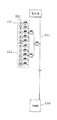
図1は、本実施の形態に係る固体撮像装置の構成の概略図である。なお、図1では、所定の単位画素101からの信号経路についてその構成の詳細が示されているが、異なる列の他の単位画素101からの信号経路も同様の構成となる。従って、以下では、所定の単位画素101からの信号経路についてのみその構成を説明する。(Embodiment 1)
FIG. 1 is a schematic diagram of a configuration of the solid-state imaging device according to the present embodiment. In FIG. 1, the details of the configuration of the signal path from the
この固体撮像装置は、入射光を光電変換して画素情報を生成する複数の単位画素(単位画素セル)101が2次元状(行列状)に配置された画素部110と、画素情報(画素信号)を保持する複数の単位メモリ105aが2次元状に配置された2次メモリ部150とを備え、単位メモリ105aの列には、同一列の複数の単位メモリ105aが単位メモリブロック105として含まれ、2次メモリ部150は、単位メモリ105aの列に対応して設けられたメモリ信号線106と、単位メモリブロック105とメモリ信号線106との間に設けられ、同じ単位メモリブロック105内の複数の単位メモリ105aで共有された1つの選択トランジスタ(選択スイッチ)t4とを有する。
This solid-state imaging device includes a
以下、図1の固体撮像装置について詳細を説明する。 Hereinafter, details of the solid-state imaging device of FIG. 1 will be described.
この固体撮像装置は、単位画素101が2次元状に配置された画素部110と、アンプ素子(アンプ回路)102が単位画素101の列毎に複数配置された1次アンプ部120と、メモリアレイである1次メモリ部130と、アンプ素子104が単位画素101の列毎に配置された2次アンプ部140と、メモリアレイである2次メモリ部150と、出力回路群160とを備える。
This solid-state imaging device includes a
出力回路群160は、例えばアナログ出力センサの場合、CDS(相関二重サンプリング)回路、水平シフトレジスタ、及び出力アンプなどで構成される。出力回路群160は、デジタル出力センサの場合、さらにADC(アナログデジタル変換回路)が単位画素101の列毎、複数の単位画素101の列毎、または所定の出力本数毎に配置される。なお、出力回路群160からの出力信号は、LVDS(low voltage differential signal)回路のような高速出力インターフェース回路で変換され出力されてもよい。
For example, in the case of an analog output sensor, the
画素部110では、光電変換素子が備えられた単位画素101がアレイ状に配置されている。なお、光電変換素子がどのような形態であっても構わない。すなわち、フォトダイオードから構成されても、光電変換膜から構成されても構わない。また、単位画素101は、複数の光電変換素子を含む多画素1セルの構造を有しても構わない。また、単位画素101は、光電変換素子及びトランジスタ等が形成された駆動回路基板における、配線等が形成される駆動回路基板の表面にレンズ等の光学系が形成され、表面から光が入射する表面照射型センサでも構わないし、駆動回路基板の裏面に光学系が形成され、裏面から光が入射する裏面照射型センサでも構わない。また、単位画素101は、駆動回路基板の表面上に光電変換膜が形成され、光電変換膜に光が入射して信号電荷が生成される積層型センサでも構わない。
In the
単位画素101は、入射光を光電変換し、信号電荷を生成する光電変換素子と、信号電荷の量に対応する信号電圧を画素情報として出力する増幅トランジスタとを有する光電変換部P(1)と、行選択トランジスタt1と、単位画素101の列に対応して設けられた画素信号線(垂直信号線)111とを有する。増幅トランジスタのソース及びドレインの一方は全単位画素101で共通の電源線と接続されている。行選択トランジスタt1は、増幅トランジスタのソース及びドレインの他方と画素信号線111との間に挿入され、画素情報を画素信号線111に出力させる。画素信号線111には、単位画素101の画素情報を画素信号線111に読み出すための定電流源(図外)が接続されている。
The
なお、光電変換部P(1)は、さらに、光電変換素子の信号電荷を蓄積し、増幅トランジスタのゲートと接続されたフローティングディフュージョン(FD)部と、ソース及びドレインの一方がFD部と接続され、他方が全単位画素で共通のリセット電圧と接続されたリセットトランジスタとを有してもよい。 Note that the photoelectric conversion unit P (1) further accumulates signal charges of the photoelectric conversion element, and a floating diffusion (FD) unit connected to the gate of the amplification transistor and one of the source and the drain are connected to the FD unit. The other may have a reset transistor connected to a common reset voltage in all unit pixels.
1次メモリ部130では、例えば画素部110の単位画素101の数に対して大幅に少ない数の単位メモリ103がアレイ状に配置されている。単位メモリ103は、単位画素101の各列に対応して同数で設けられている。単位メモリ103は、アンプ素子102を介して画素信号線111と接続されたスイッチとしての書き込みトランジスタt3と、書き込みトランジスタt3により書き込まれた画素信号線111の画素情報を保持する容量m1(1)と、容量m1(1)に保持された画素情報を読み出す読み出しトランジスタt2とから構成されている。
In the
1次アンプ部120は入力信号(画素部110からの画素情報)を後段の1次メモリ部130へ書き込むための駆動回路であり、2次アンプ部140は入力信号(1次メモリ部130に保持されている画素情報)を後段の2次メモリ部150へ書き込むための駆動回路である。1次アンプ部120及び2次メモリ部150は、例えば直流カット容量、バイアス印加回路、及びソースフォロア回路などで構成されるが、設計によってCDS回路なども含まれてもよい。1次アンプ部120は、単位画素101の各列に対応して設けられたアンプ素子102から構成されている。同様に、2次アンプ部140は、単位画素101の各列に対応して設けられたアンプ素子104から構成されている。
The
次に、2次メモリ部150の構成について詳細に説明する。
Next, the configuration of the
2次メモリ部150では、小メモリ群である複数の単位メモリブロック105がアレイ状に配置されている。単位メモリブロック105は、同じ列の単位メモリ105aから構成されており、単位画素101の列に対応して複数設けられている。単位メモリ105aの列は単位画素101の列に対応付けられており、対応する単位画素101の信号を保持する。なお、単位メモリ105aの行数は単位画素101の行数以上、例えば両者の行数は同じであり、各単位画素101の画素情報を同時期に異なる単位メモリ105aで保持してもよい。
In the
2次メモリ部150は、アンプ素子104と接続されたメモリ信号線106と、メモリ信号線106と単位メモリブロック105との間に挿入された選択トランジスタt4とを有する。選択トランジスタt4は、複数の単位メモリブロック105のそれぞれに対応して個別に設けられている。
The
単位メモリ105aは、選択トランジスタt4を介してメモリ信号線106と接続された書き込みトランジスタt5と、書き込みトランジスタt5により書き込まれた画素情報(メモリ信号線106の信号電圧)を保持する容量m2(1)と、容量112に保持された画素情報を読み出す読み出しトランジスタt2とから構成されている。なお、他の単位メモリ105aもこれと同様の構成を有する。例えば、他の単位メモリ105aは、書き込みトランジスタt7と、容量m2(2)と、読み出しトランジスタt8とから構成されている。さらに他の単位メモリ105aは、書き込みトランジスタt9と、容量m2(k)と、読み出しトランジスタt10とから構成されている。
The
この2次メモリ部150では、選択トランジスタt4がオンされるとメモリ信号線106と単位メモリブロック105とが導通し、オフされると絶縁する。そして、例えば、選択トランジスタt4がオンしている時に、書き込みトランジスタt5がオンすればメモリ信号線106の信号電圧が容量m2(1)に格納される。この方法で書き込みトランジスタt5、t7及びt9を選択的にオンすることで単位メモリブロック105内の画素情報を格納する容量が選択される。同じメモリ信号線106に接続された異なる単位メモリブロック105でもこれと同様の方法により操作できる。
In the
次に、本実施の形態に係る固体撮像装置の駆動方法について図2を用いて説明する。 Next, a method for driving the solid-state imaging device according to the present embodiment will be described with reference to FIG.
図2は、固体撮像装置の駆動方法を示すタイミングチャートである。 FIG. 2 is a timing chart showing a method for driving the solid-state imaging device.
なお、図2において、oe(a)(aは整数)は単位画素101からの出力をオンオフ(行選択トランジスタt1のオンオフを制御)する制御信号である。また、m1w(b)(bは整数)は1次メモリ部130の容量m1(b)への書き込みを制御(書き込みトランジスタt3のオンオフを制御)する制御信号である。また、m1r(c)(cは整数)は1次メモリ部130の容量m1(c)からの読み出しを制御(読み出しトランジスタt2のオンオフを制御)する制御信号である。また、例えばDk(kは整数)とは単位画素101のリセット信号(単位画素101のリセット時の信号電圧)を意味し、Lkとは単位画素101の明信号(光電変換により単位画素101で生成された信号電荷に対応する信号電圧)を意味している。また、Xとは不定データを意味している。また、m2b(e)(eは整数)は2次メモリ部150のメモリ信号線106と単位メモリブロック105との導通を制御(選択トランジスタt4のオンオフを制御)するブロック制御信号を意味している。また、m2r(f)(fは整数)は2次メモリ部150の容量m2(f)に保持されたデータを読み出す際の読み出す容量を選択(読み出しトランジスタt6、t8及びt10のオンオフを制御)する制御信号を意味している。また、m2w(g)(gは整数)は2次メモリ部150の容量m2(f)にデータを書き込む際の書き込む容量を選択(書き込みトランジスタt5、t7及びt9のオンオフを制御)する制御信号を意味している。また、容量m2(h)に保持されているデータとして、例えばL1−D1は単位画素101の明信号からリセット信号を差分した信号を意味している。
In FIG. 2, oe (a) (a is an integer) is a control signal for turning on / off the output from the unit pixel 101 (controlling on / off of the row selection transistor t1). M1w (b) (b is an integer) is a control signal for controlling writing to the capacitor m1 (b) of the primary memory unit 130 (controlling on / off of the writing transistor t3). Further, m1r (c) (c is an integer) is a control signal for controlling reading from the capacitor m1 (c) of the primary memory unit 130 (controlling on / off of the reading transistor t2). For example, Dk (k is an integer) means a reset signal of the unit pixel 101 (signal voltage when the
まず、制御信号oe(1)を時刻t1でハイレベルにして選択トランジスタt1をオンすることで、単位画素101のリセット信号D1が画素部110の画素信号線111に供給される。同時に時刻t1で、リセット信号D1は1次アンプ部120により1次メモリ部130に書き込まれる。つまり、制御信号m1w(1)をハイレベルにして書き込みトランジスタt3をオンすることにより、1次メモリ部130の容量m1(1)にD1データが書き込まれる。その後、明信号Lkとリセット信号Dkとが交互に単位画素101のそれぞれから図2のようなシーケンスで読み出される。
First, the control signal oe (1) is set to the high level at time t1 to turn on the selection transistor t1, whereby the reset signal D1 of the
次に、制御信号m2b(1)及びm2w(1)を時刻t6でハイレベルにして選択トランジスタt4及び書き込みトランジスタt5をオンすることで、単位画素101の画素情報が1次メモリ部130の容量m1(1)から2次メモリ部150の容量m2(1)に書き込まれる。このとき、例えば回路設計の一例として2次アンプ部140にCDS回路を含めていれば、2次メモリ部150に格納されるデータは明信号L1からリセット信号D1を差分した信号となる。このことは時刻t6で容量m2(1)にL1−D1のデータが格納されていることに示されている。
Next, the control signals m2b (1) and m2w (1) are set to the high level at time t6 to turn on the selection transistor t4 and the write transistor t5, whereby the pixel information of the
この時刻t6においてブロック制御信号m2b(1)をオンすることで、容量m2(1)への書きこみを成功させるが、この時、非選択の単位メモリブロック105とメモリ信号線106との間の選択トランジスタt4はオフしていることに注意する。非選択の単位メモリブロック105とメモリ信号線106との間の選択トランジスタt4がオフしていることで2次メモリ部150の共通信号線であるメモリ信号線106に接続される非選択(オフ状態)のトランジスタ数は選択されている単位メモリブロック105内の非選択(オフ状態)の書き込みトランジスタの数である(k−1)個(kは単位メモリブロック105内の書き込みトランジスタの総数)と単位メモリブロック105の数であるM個の合計M+k−1となる。この時、もし2次メモリ部150を複数のブロックに分けて構成しなかった場合では、(M×k+k−1)の非選択のトランジスタがメモリ信号線106に接続されることになる。非選択のトランジスタの接合容量、及びゲート電極とドレイン部とのカップリング容量などがメモリ信号線106に接続されているトランジスタの分だけ並列で接続されるので、この寄生容量分を全て充放電することがアンプ素子104には要求される。この充放電はもちろん信号に依存しているが、例えば明暗差の大きい信号が横方向に多数混在している場合、アンプ素子104で電流を大量に流す必要があり、アンプ素子104につながる電源線のインピーダンス成分の為に電圧降下を起こしてしまい、画像データにおける横引きの雑音現象を生じてしまう。これは、例えば図3Bに示されている。図3Bは、図3Aの高輝度被写体を撮像した場合における、横引きノイズが発生した画像を示す図である。しかしながら、2次メモリ部150を複数のブロックに分けて構成にして2次メモリ部150のメモリ信号線106に接続される寄生容量を小さくすることで、アンプ素子104が充放電する電荷量はすくなくなる。その結果、アンプ素子104に供給される電源線の電圧低下は低減できる。
At this time t6, the block control signal m2b (1) is turned on to successfully write to the capacitor m2 (1). At this time, the connection between the unselected
以上のような動作を行うことで全てのデータ(全ての単位画素101の画素情報)に関して同様に連続的に2次メモリ部150まで書きこむことで、高速に2次メモリ部150へ書き込み、かつ、横引きノイズのない画像を2次メモリ部150上に得ることができる。
By performing the operation as described above, all the data (pixel information of all the unit pixels 101) are similarly written continuously to the
次に、2次メモリ部150のデータを読み出し、出力する。2次メモリ部150に書きこまれたデータは出力回路群160を介して出力される。このとき、アナログ出力の固体撮像装置であれば、出力回路群160はCDS回路、水平シフトレジスタ、及びソースフォロア出力回路等から構成され、例えば60fpsなどの所定の周期でフレームデータをアナログ信号で出力する。一方、デジタル出力の固体撮像装置であれば、出力回路群160はCDS、ADC及びLVDS回路等で構成され、デジタルデータを出力する。
Next, the data in the
以上のように本実施の形態の固体撮像装置によれば、2次メモリ部150は複数の単位メモリブロック105で構成され、単位メモリブロック105はそれぞれに対応して設けられた選択トランジスタt4を介してメモリ信号線106と接続される。従って、メモリ信号線106の寄生容量を低減することができるので、2次メモリ部150への画素情報の書き込みを高速にし、かつ、横筋ノイズ等の発生を抑えることができる。
As described above, according to the solid-state imaging device of the present embodiment, the
なお、本実施の形態において、固体撮像装置は、信号処理回路などを混載するような設計でも構わない。また、1次メモリ部130及び2次メモリ部150を構成する容量の構成は電圧保持する容量型の記憶素子であれば形態を限定されない。
In the present embodiment, the solid-state imaging device may be designed so as to incorporate a signal processing circuit or the like. Further, the configuration of the capacitors constituting the
また、本実施の形態において、固体撮像装置の2次メモリ部150のブロック構成は、一段のみの構成ではなく多段の構成であっても構わない。例えば、2次メモリ部150は、図4に示すような2段の構成を有しても構わない。この構成では、選択トランジスタt4と読み出しトランジスタt5、t7、t9及びt11との間に選択トランジスタt4a及びt4bが設けられる。
In the present embodiment, the block configuration of the
また、本実施の形態において、単位メモリ105aの列には、複数の単位メモリブロック105が含まれるとしたが、1つだけしか含まれなくてもよい。つまり、単位メモリ105aの列に対して1つの選択トランジスタt4しか設けられなくてもよい。
In the present embodiment, the
(実施の形態2)
実施の形態1では2次メモリ部150がブロック構成にされているため、2次メモリ部150内においてメモリ信号線106とは別に単位メモリブロック105内に信号線が設けられ、信号線が単位画素101の各列に対応して2本存在している。そのため、2次メモリ部150の単位面積はブロック構成にすることで大きくなってしまっている。実施の形態2の構成は、この面積課題を軽減する効果を生むものである。(Embodiment 2)
In the first embodiment, since the
図5は、本実施の形態に係る1次メモリ部130、2次アンプ部140及び2次メモリ部150の構成を示す図である。なお、図5では2列分の単位画素101からの信号経路についてのみ抽象化して記載している。以下では、実施の形態1と異なる点についてのみ述べる。
FIG. 5 is a diagram showing a configuration of the
この固体撮像装置は、1つのメモリ信号線106が単位メモリ105aの複数列で共有される点で実施の形態1と異なる。また、CDS回路を含み、画素情報を2次メモリ部150に書きこむ信号駆動部を2次アンプ部140として備え、1つの信号駆動部は単位メモリ105aの複数列で共有される点でも実施の形態1と異なる。
This solid-state imaging device is different from the first embodiment in that one
この構成では、メモリ信号線106を共有する異なる列の単位メモリブロック105とメモリ信号線106との間に設けられた異なる選択トランジスタt4を異なるタイミングでオンするように固体撮像装置が駆動される。また、1つの信号駆動部に対し、異なる列の単位画素101の画素情報を選択的に異なるタイミングで入力するように固体撮像装置が駆動される。そして、画素部110から信号駆動部に画素情報を読み出す基本周波数に対して、信号駆動部を駆動する駆動周波数は逓倍である。
In this configuration, the solid-state imaging device is driven so that different selection transistors t4 provided between the unit memory blocks 105 in different columns sharing the
2つの単位メモリブロック105の列のそれぞれは、異なる単位画素101の列に対応して設けられている。2次メモリ部150内には、メモリ信号線106と、一方の列の単位メモリブロック105内の信号線と、他方の列の単位メモリブロック105内の信号線との3本の信号線が列方向に走る信号線として存在している。従って、図1の構成と比較して1列の単位メモリブロック105あたり1.5本に信号線の本数を減らすことに成功している。このように設計の方針として面積を重視する場合、共通信号線方式も可能である。その場合1次メモリ部130からの書き込み速度は単位画素101からの転送速度の2倍にする必要がある。このことを示した簡易タイミングチャートを図6に示す。図6は、メモリ信号線106を共有する隣り合う2つの単位画素101の列(第N(Nは自然数)列及び第N+1列)の画素情報について、1次メモリ部130への書き込み(図6のt1〜t4)及び1次メモリ部130からの読み出し(図6のt5〜t12)のタイミングを示している。なお、図6では、単位画素101のリセット信号を「dark」で示し、画素信号を「signal」で示している。1次メモリ部130とCDS回路とをつなぐ選択トランジスタt20及びt21を相補で駆動し、さらにメモリ信号線106と左右の異なる列の単位メモリブロック105とをそれぞれつなぐ2つの選択トランジスタt4を相補で駆動することで、1次メモリ部130の信号を共通のCDS回路及びアンプ素子104つまり共通の2次アンプ部140を用いて2次メモリ部150に格納することができる。
Each of the columns of the two unit memory blocks 105 is provided corresponding to a column of
以上のように本実施の形態の固体撮像装置によれば、メモリ信号線106が単位メモリブロック105の複数列で共有されるため、小型化を実現することができる。
As described above, according to the solid-state imaging device of the present embodiment, since the
(実施の形態3)
実施の形態1では2次メモリ部150がブロック構成にされているが、本実施の形態では画素部110がブロック構成にされている。(Embodiment 3)
Although the
図7は、本実施の形態の固体撮像装置の画素部110の構成を示す図である。なお、図7では、所定の一列の単位画素101のみを抽象化して記載している。以下では、実施の形態1と異なる点についてのみ述べる。
FIG. 7 is a diagram illustrating a configuration of the
この固体撮像装置は、単位画素101の列に、同一列の複数の単位画素101が単位画素ブロック121として含まれ、画素部110は、単位画素101の列に対応して設けられた画素信号線111と、単位画素ブロック121と画素信号線111との間に設けられ、同じ単位画素ブロック121内の複数の単位画素101で共有された1つの選択トランジスタ(選択スイッチ)t31とを有する点で実施の形態1と異なる。
In the solid-state imaging device, a plurality of
同一列の複数の単位画素101は複数ブロックにまとめられ、ブロック毎に選択トランジスタt31が備えられ、その選択トランジスタt31は画素信号線111に接続されている。そして、行選択トランジスタt1は対応する光電変換部Pと選択トランジスタt31との間に挿入されている。この構成により、画素信号線111につながるトランジスタの数を減らすことが可能になる。その結果、単位画素101からの信号を高速にメモリへ書きこむように画素信号線111を駆動することができる。
A plurality of
以上のように本実施の形態の固体撮像装置によれば、画素部110は複数の単位画素ブロック121で構成され、単位画素ブロック121はそれぞれに対応して設けられた選択トランジスタt31を介して画素信号線111と接続される。従って、画素信号線111の寄生容量を低減することができるので、画素信号線111への信号の読み出しを高速にし、かつ、横筋ノイズ等の発生を抑えることができる。
As described above, according to the solid-state imaging device of the present embodiment, the
なお、本実施の形態において、2次メモリ部150はブロック構成にされていなくてもよい。
In the present embodiment, the
また、本実施の形態において、固体撮像装置の画素部110のブロック構成は、一段のみの構成ではなく多段の構成であっても構わない。例えば、画素部110は、図8に示すような2段の構成を有しても構わない。この構成では、選択トランジスタt31と行選択トランジスタt1との間に選択トランジスタt32が設けられる。
In the present embodiment, the block configuration of the
また、本実施の形態において、単位画素101の列には、複数の単位画素ブロック121が含まれるとしたが、1つだけしか含まれなくてもよい。つまり、単位画素101の列に対して1つの選択トランジスタt31しか設けられなくてもよい。
In the present embodiment, the
(実施の形態4)
図9は、本発明における実施の形態の撮像装置(カメラシステム)の全体構成を示す図である。(Embodiment 4)
FIG. 9 is a diagram illustrating an overall configuration of the imaging apparatus (camera system) according to the embodiment of the present invention.
この撮像装置は、大きく分けて固体撮像装置200、光学系240、DSP(Digital Signal Processor)250、液晶画面等の画像表示デバイス280及び画像メモリ290から構成されている。
This imaging apparatus is roughly composed of a solid-
光学系240は、被写体からの光を集光して固体撮像装置200の画素部110上に画像イメージを形成するレンズ241を備えている。
The
固体撮像装置200は、実施の形態1〜3で説明した固体撮像装置である。固体撮像装置200は、単位画素101を2次元配列状に並べた画素部110と、画素部110の単位画素101を行単位で選択し、単位画素101のリセット及び信号読み出しを制御信号を出力して制御する垂直選択回路220と、垂直選択回路220に駆動パルスを供給するタイミング制御部230とを備えている。
The solid-
DSP250は、カメラシステム制御部260及び画像処理回路270を備えている。
The
画像処理回路270は、固体撮像装置200から出力されたデジタル画素信号を受けて、カメラ信号処理として必要な、ガンマ補正、色補間処理、空間補間処理、及びオートホワイトバランス等の処理を行う。また、画像処理回路270は、JPEG等の圧縮フォーマットへの変換、画像メモリ290への記録、及び画像表示デバイス280への表示用信号処理等を行う。
The
カメラシステム制御部260は、ユーザI/F(図示せず)で指定された各種の設定に従って、光学系240、固体撮像装置200及び画像処理回路270の制御を行い、撮像装置の全体動作を統合するマイクロコンピュータ等である。ユーザI/Fは、例えば、ズーム倍率の変更及びレリーズボタンなどのリアルタイム指示を入力として受け、カメラシステム制御部260は、レンズ241のズーム倍率変更、幕シャッタの走行及び固体撮像装置200のリセット走査の制御を行う。
The camera
以上、本発明の固体撮像装置、固体撮像装置の駆動方法及び撮像装置について、実施の形態に基づいて説明したが、本発明は、これらの実施の形態に限定されるものではない。本発明の要旨を逸脱しない範囲内で当業者が思いつく各種変形を施したものも本発明の範囲内に含まれる。また、発明の趣旨を逸脱しない範囲で、複数の実施の形態における各構成要素を任意に組み合わせてもよい。 As described above, the solid-state imaging device, the driving method of the solid-state imaging device, and the imaging device of the present invention have been described based on the embodiments. However, the present invention is not limited to these embodiments. The present invention includes various modifications made by those skilled in the art without departing from the scope of the present invention. Moreover, you may combine each component in several embodiment arbitrarily in the range which does not deviate from the meaning of invention.
本発明は、固体撮像装置、固体撮像装置の駆動方法及び撮像装置に利用が可能であり、特にデジタルスチルカメラ、デジタルビデオカメラ及びカメラ付携帯電話機などに利用が可能であり、産業上有用である。 INDUSTRIAL APPLICABILITY The present invention can be used for a solid-state imaging device, a driving method of the solid-state imaging device, and an imaging device, and can be used particularly for a digital still camera, a digital video camera, a camera-equipped mobile phone, and the like, and is industrially useful. .
1 単位画素セル
2 画素部
5 水平選択部
11 水平信号線
12 出力アンプ
21 メモリセル
22 メモリ部
31 ノイズ抑圧部
101 単位画素
102、104 アンプ素子
103、105a 単位メモリ
105 単位メモリブロック
106 メモリ信号線
110 画素部
111 画素信号線
112 容量
120 1次アンプ部
121 単位画素ブロック
130 1次メモリ部
140 2次アンプ部
150 2次メモリ部
160 出力回路群
200 固体撮像装置
220 垂直選択回路
230 タイミング制御部
240 光学系
241 レンズ
250 DSP
260 カメラシステム制御部
270 画像処理回路
280 画像表示デバイス
290 画像メモリ
DESCRIPTION OF
260 Camera
本発明は、メモリ内蔵の固体撮像装置に関し、特に列方向のメモリの分割方法の技術、すなわち固体撮像装置のカラムメモリの多ブロック配置に関する。 The present invention relates to a solid-state imaging device with a built-in memory, and more particularly to a technique for dividing a memory in a column direction, that is, a multi-block arrangement of column memories of a solid-state imaging device.
従来、画素情報を一旦メモリに貯めて出力する技術として特許文献1が開示されている。特許文献1の固体撮像装置を図10に示す。
Conventionally,
この固体撮像装置は、画素部2と、垂直走査部(図外)と、単位画素セル1の選択行からの画素信号のノイズを抑圧するノイズ抑圧部31と、メモリセル21を有し、ノイズ抑圧部31の出力信号を蓄積するメモリ部22と、メモリ用垂直走査部(図外)と、水平選択部5と、水平信号線11と、出力アンプ12とを備える。
This solid-state imaging device includes a
しかしながら、従来の技術におけるメモリ内蔵の固体撮像装置では、画素情報をメモリ部22に格納する速度を速めた場合、ストリーキングが発生する。図3Bにストリーキング発生時の画像を示している。ストリーキングとは、高輝度被写体が存在する場合、電流が多く流れる単位画素セル1の列が多くなり、その結果、単位画素セル1の各列に供給する電源電圧が異なってくることに起因する横筋の不具合である。メモリ部22の信号線に接続される非選択のメモリセル21のメモリ書き込みトランジスタM31の拡散容量等の総容量を充放電するためにアンプA15で消費される電流が、高輝度被写体撮像時に多くなるため、高速書き込みの際には、アンプA15に供給される電源線の電圧降下が発生することにより、ストリーキングは発生する。
However, in the conventional solid-state imaging device with a built-in memory, streaking occurs when the speed of storing pixel information in the
そこで、本発明は、かかる問題点に鑑み、横筋ノイズ等の発生を抑えることが可能な固体撮像装置、固体撮像装置の駆動方法および撮像装置を提供することを目的とする。 SUMMARY OF THE INVENTION In view of the above problems, an object of the present invention is to provide a solid-state imaging device, a driving method of the solid-state imaging device, and an imaging device that can suppress the occurrence of horizontal stripe noise and the like.
本発明の一態様に係る固体撮像装置は、入射光を光電変換して画素情報を生成する複数の単位画素が2次元状に配置された画素部と、前記画素情報を保持する複数の単位メモリが行列状に配置されたメモリ部とを備え、前記単位メモリの列には、同一列の複数の前記単位メモリが単位メモリブロックとして含まれ、前記メモリ部は、前記単位メモリの列に対応して設けられたメモリ信号線と、前記単位メモリブロックと前記メモリ信号線との間に設けられ、同じ前記単位メモリブロック内の複数の前記単位メモリで共有された1つの選択スイッチとを有し、前記単位メモリは、書き込みトランジスタと、容量と、読み出しトランジスタとから構成されていることを特徴とする。つまり、カラムメモリ(同一列の単位メモリ)をブロック構成にすることで、単位メモリにつながるメモリ信号線に接続されるスイッチの数を格段に少なくすることができる。そのため、メモリ信号線と接続された非選択状態のスイッチの拡散容量に起因する寄生容量の総和を低減することが可能になる。容量を低減することにより、信号を単位メモリに書きこむ際(メモリ信号線を駆動する際)の駆動回路で消費する電流を低減することが可能になり、駆動回路に供給する電源線のインピーダンス成分で発生する電圧降下の影響を小さくできる。電源線の電圧降下が小さくなることにより高輝度被写体の撮像時においても横筋ノイズ等の発生を抑えることができる。また、高速で単位メモリに信号転送することが可能になる。 A solid-state imaging device according to one embodiment of the present invention includes a pixel unit in which a plurality of unit pixels that generate pixel information by photoelectrically converting incident light are two-dimensionally arranged, and a plurality of unit memories that hold the pixel information And the unit memory column includes a plurality of unit memories in the same column as unit memory blocks, and the memory unit corresponds to the unit memory column. a memory signal line provided Te, provided between said memory signal line and the unit memory block, possess a single selection switches that are shared by a plurality of unit memory of the same said unit memory block, The unit memory is composed of a write transistor, a capacitor, and a read transistor . In other words, the column memory (unit memory in the same column) has a block configuration, and the number of switches connected to the memory signal line connected to the unit memory can be significantly reduced. For this reason, it is possible to reduce the total parasitic capacitance caused by the diffusion capacitance of the non-selected switch connected to the memory signal line. By reducing the capacity, it becomes possible to reduce the current consumed by the drive circuit when writing a signal to the unit memory (when driving the memory signal line), and the impedance component of the power supply line supplied to the drive circuit Can reduce the influence of the voltage drop. By reducing the voltage drop of the power supply line, it is possible to suppress the occurrence of horizontal stripe noise or the like even when imaging a high-luminance subject. Further, it becomes possible to transfer signals to the unit memory at high speed.
ここで、1つの前記メモリ信号線は、複数列の前記単位メモリで共有されてもよい。つまり、メモリ信号線を複数列の単位メモリで共有化にすることで、コンパクトなメモリレイアウトが可能になる。メモリ部の面積の縮小が可能になるので、チップコストを下げることができる。 Here, one memory signal line may be shared by a plurality of columns of the unit memories. That is, by sharing the memory signal line among the unit memories of a plurality of columns, a compact memory layout becomes possible. Since the area of the memory portion can be reduced, the chip cost can be reduced.
また、固体撮像装置は、さらに、前記画素情報を前記メモリ部に書きこむ信号駆動部を備え、1つの前記信号駆動部は、前記単位メモリの複数列で共有されてもよい。つまり、信号駆動部を複数列の単位メモリで共有化にすることで、コンパクトな信号駆動部のレイアウトが可能になる。信号駆動部の面積の縮小が可能になるので、チップコストを下げることができる。 The solid-state imaging device may further include a signal driving unit that writes the pixel information in the memory unit, and one signal driving unit may be shared by a plurality of columns of the unit memory. In other words, by sharing the signal driver with a plurality of columns of unit memories, a compact signal driver layout can be achieved. Since the area of the signal driver can be reduced, the chip cost can be reduced.
また、本発明の一態様に係る固体撮像装置は、入射光を光電変換して画素情報を生成する複数の単位画素が2次元状に配置された画素部と、前記画素情報を保持する複数の単位メモリが2次元状に配置されたメモリ部と、を備え、前記単位画素の列には、同一列の複数の前記単位画素が単位画素ブロックとして含まれ、前記画素部は、前記単位画素の列に対応して設けられた画素信号線と、前記単位画素ブロックと前記画素信号線との間に設けられ、同じ前記単位画素ブロック内の複数の前記単位画素で共有された1つの選択スイッチとを有し、前記単位メモリは、書き込みトランジスタと、容量と、読み出しトランジスタとから構成されていることを特徴とする。つまり、同一列の単位画素群をブロック構成にすることで、単位画素につながる画素信号線に接続されるスイッチの数を格段に少なくすることができる。そのため、画素信号線と接続された非選択状態のスイッチの拡散容量に起因する寄生容量の総和を低減することが可能になる。容量を低減することにより、画素信号線に信号を読み出す際(画素信号線を駆動する際)の駆動回路で消費する電流を低減することが可能になり、駆動回路に供給する電源線のインピーダンス成分で発生する電圧降下の影響を小さくできる。電源線の電圧降下が小さくなることにより高輝度被写体の撮像時においても横筋ノイズ等の発生を抑えることができる。また、高速で画素信号線に信号転送することが可能になる。 In addition, a solid-state imaging device according to one embodiment of the present invention includes a pixel portion in which a plurality of unit pixels that photoelectrically convert incident light to generate pixel information are two-dimensionally arranged, and a plurality of pixel information that holds the pixel information A memory unit in which unit memories are two-dimensionally arranged, and the unit pixel column includes a plurality of unit pixels in the same column as a unit pixel block, and the pixel unit includes the unit pixels. A pixel signal line provided corresponding to a column, and one selection switch provided between the unit pixel block and the pixel signal line and shared by the plurality of unit pixels in the same unit pixel block; have a, the unit memory is characterized with the writing transistor, and a capacitor, that is composed of a read transistor. That is, the number of switches connected to the pixel signal line connected to the unit pixel can be remarkably reduced by making the unit pixel group in the same column into a block configuration. For this reason, it is possible to reduce the total parasitic capacitance due to the diffusion capacitance of the non-selected switch connected to the pixel signal line. By reducing the capacitance, it is possible to reduce the current consumed by the drive circuit when reading a signal to the pixel signal line (when driving the pixel signal line), and the impedance component of the power supply line supplied to the drive circuit Can reduce the influence of the voltage drop. By reducing the voltage drop of the power supply line, it is possible to suppress the occurrence of horizontal stripe noise or the like even when imaging a high-luminance subject. Further, it becomes possible to transfer the signal to the pixel signal line at high speed.
また、前記単位画素は、入射光を光電変換し、信号電荷を生成する光電変換素子と、前記信号電荷の量に対応する信号電圧を画素情報として出力する増幅トランジスタと、前記信号電圧を前記画素信号線に出力させる行選択トランジスタとを有してもよい。 The unit pixel includes a photoelectric conversion element that photoelectrically converts incident light to generate a signal charge, an amplification transistor that outputs a signal voltage corresponding to the amount of the signal charge as pixel information, and the signal voltage to the pixel. A row selection transistor for outputting to the signal line may be included.
また、本発明の一態様に係る固体撮像装置の駆動方法は、固体撮像装置の駆動方法であって、前記固体撮像装置は、入射光を光電変換して画素情報を生成する複数の単位画素が2次元状に配置された画素部と、前記画素情報を保持する複数の単位メモリが2次元状に配置されたメモリ部とを備え、前記単位メモリの列には、同一列の複数の前記単位メモリが単位メモリブロックとして含まれ、前記メモリ部は、前記単位メモリの列に対応して設けられたメモリ信号線と、前記単位メモリブロックと前記メモリ信号線との間に設けられ、同じ前記単位メモリブロック内の複数の前記単位メモリで共有された1つの選択スイッチとを有し、1つの前記メモリ信号線は、前記単位メモリの複数列で共有され、前記固体撮像装置の駆動方法では、前記メモリ信号線を共有する異なる列の前記単位メモリブロックと前記メモリ信号線との間に設けられた異なる選択スイッチを異なるタイミングでオンすることを特徴とする。つまり、選択スイッチを異なる単位メモリの列毎に走査することで、メモリ信号線を異なる列の単位メモリで共用することが可能になる。 The solid-state imaging device driving method according to one aspect of the present invention is a solid-state imaging device driving method, and the solid-state imaging device includes a plurality of unit pixels that generate pixel information by photoelectrically converting incident light. A pixel unit arranged in a two-dimensional manner and a memory unit in which a plurality of unit memories holding the pixel information are arranged in a two-dimensional manner, and the unit memory column includes a plurality of the units in the same column A memory is included as a unit memory block, and the memory unit is provided between a memory signal line provided corresponding to a column of the unit memory and between the unit memory block and the memory signal line, and the same unit. One selection switch shared by a plurality of unit memories in a memory block, and one memory signal line is shared by a plurality of columns of the unit memories. In the driving method of the solid-state imaging device, Characterized by turning on the different selection switch at different times provided between different column the unit memory blocks sharing the memory signal line and the memory signal line. That is, by scanning the selection switch for each column of different unit memories, the memory signal lines can be shared by the unit memories of different columns.
また、前記固体撮像装置は、さらに、前記画素情報を前記メモリ部に書きこむ信号駆動部を備え、1つの前記信号駆動部は、前記単位メモリの複数列で共有され、かつ前記単位画素の複数列で共有され、前記固体撮像装置の駆動方法では、1つの前記信号駆動部に対し、異なる列の前記単位画素の画素情報を選択的に異なるタイミングで入力してもよい。つまり信号駆動部に選択的に異なる列の単位画素の信号を入力することで、信号駆動部を異なる列の単位画素で共用することが可能になる。 The solid-state imaging device further includes a signal driving unit that writes the pixel information to the memory unit. One signal driving unit is shared by a plurality of columns of the unit memory, and a plurality of the unit pixels are included. In the driving method of the solid-state imaging device shared by the columns, pixel information of the unit pixels in different columns may be selectively input at different timings to one signal driving unit. That is, by selectively inputting the signals of the unit pixels in different columns to the signal driver, the signal driver can be shared by the unit pixels in different columns.
また前記画素部から前記信号駆動部に画素情報を読み出す基本周波数に対して、前記信号駆動部を駆動する駆動周波数が逓倍であってもよい。つまり、単位メモリへ信号を書きこむ周波数を単位画素から信号を読み出す基本周波数に対して逓倍にすることで、メモリ信号線を異なる単位メモリの列で共有化しても信号の読み出しとメモリ書き込みとを滞りなく実施することが可能になる。従って、メモリ部の面積を削減してもタイミングロスが生じない。 In addition, the driving frequency for driving the signal driving unit may be multiplied with respect to a fundamental frequency for reading pixel information from the pixel unit to the signal driving unit. In other words, by multiplying the frequency at which a signal is written into the unit memory with respect to the basic frequency at which the signal is read out from the unit pixel, even if the memory signal line is shared by different unit memory columns, signal reading and memory writing are performed. It becomes possible to carry out without delay. Therefore, timing loss does not occur even if the area of the memory portion is reduced.
また、本発明の一態様に係る撮像装置は、固体撮像装置を備えることを特徴としてもよい。つまり、上記固体撮像装置を撮像装置に使用することで、極めてグローバルシャッター動作に近い動作が可能で、かつ、画質の劣化が少ない撮像装置を提供することが可能になる。 The imaging device according to one embodiment of the present invention may include a solid-state imaging device. That is, by using the solid-state imaging device for the imaging device, it is possible to provide an imaging device that can operate extremely close to a global shutter operation and that has little deterioration in image quality.
本発明により、カラムメモリ又は同一列の単位画素群をブロック構成にすることで、メモリ信号線又は画素信号線の寄生容量を低減することが可能になる。容量を低減することにより、信号をメモリに書きこむ際又は画素信号線に読み出す際の駆動回路で消費する電流を低減することが可能になり、駆動回路に供給する電源線のインピーダンス成分で発生する電圧降下の影響を小さくできる。電源線の電圧降下が小さくなることにより高輝度被写体の撮像時においても横筋ノイズ等の発生を抑えることができる。また、高速で画素信号線又はメモリに信号転送することが可能になる。 According to the present invention, the column memory or the unit pixel group in the same column is configured as a block, so that the parasitic capacitance of the memory signal line or the pixel signal line can be reduced. By reducing the capacity, it is possible to reduce the current consumed by the driver circuit when writing a signal to the memory or reading the signal to the pixel signal line, and it is generated by the impedance component of the power supply line supplied to the driver circuit. The effect of voltage drop can be reduced. By reducing the voltage drop of the power supply line, it is possible to suppress the occurrence of horizontal stripe noise or the like even when imaging a high-luminance subject. Further, it becomes possible to transfer the signal to the pixel signal line or the memory at high speed.
以下、本発明に係る実施の形態について、図面を参照しながら、さらに具体的に説明する。なお、本発明について、以下の実施の形態及び添付の図面を用いて説明を行うが、これは例示を目的としており、本発明がこれらに限定されることを意図しない。つまり、以下の実施の形態で示される構成要素、構成要素の配置位置及び接続形態、タイミング、タイミングの順序などは、一例であり、本発明を限定する主旨ではない。本発明は、特許請求の範囲だけによって限定される。よって、以下の実施の形態における構成要素のうち、本発明の最上位概念を示す独立請求項に記載されていない構成要素については、本発明の課題を達成するのに必ずしも必要ではないが、より好ましい形態を構成するものとして説明される。また、図面において、実質的に同一の構成、動作、および効果を表す要素については、同一の符号を付す。 Hereinafter, embodiments according to the present invention will be described more specifically with reference to the drawings. In addition, although this invention is demonstrated using the following embodiment and attached drawing, this is for the purpose of illustration and this invention is not intended to be limited to these. That is, the constituent elements, the arrangement positions and connection forms of the constituent elements, the timing, the order of timings, and the like shown in the following embodiments are merely examples, and are not intended to limit the present invention. The invention is limited only by the claims. Therefore, among the constituent elements in the following embodiments, constituent elements that are not described in the independent claims indicating the highest concept of the present invention are not necessarily required to achieve the object of the present invention. It will be described as constituting a preferred form. In the drawings, elements that represent substantially the same configuration, operation, and effect are denoted by the same reference numerals.
(実施の形態1)
図1は、本実施の形態に係る固体撮像装置の構成の概略図である。なお、図1では、所定の単位画素101からの信号経路についてその構成の詳細が示されているが、異なる列の他の単位画素101からの信号経路も同様の構成となる。従って、以下では、所定の単位画素101からの信号経路についてのみその構成を説明する。
(Embodiment 1)
FIG. 1 is a schematic diagram of a configuration of the solid-state imaging device according to the present embodiment. In FIG. 1, the details of the configuration of the signal path from the
この固体撮像装置は、入射光を光電変換して画素情報を生成する複数の単位画素(単位画素セル)101が2次元状(行列状)に配置された画素部110と、画素情報(画素信号)を保持する複数の単位メモリ105aが2次元状に配置された2次メモリ部150とを備え、単位メモリ105aの列には、同一列の複数の単位メモリ105aが単位メモリブロック105として含まれ、2次メモリ部150は、単位メモリ105aの列に対応して設けられたメモリ信号線106と、単位メモリブロック105とメモリ信号線106との間に設けられ、同じ単位メモリブロック105内の複数の単位メモリ105aで共有された1つの選択トランジスタ(選択スイッチ)t4とを有する。
This solid-state imaging device includes a
以下、図1の固体撮像装置について詳細を説明する。 Hereinafter, details of the solid-state imaging device of FIG. 1 will be described.
この固体撮像装置は、単位画素101が2次元状に配置された画素部110と、アンプ素子(アンプ回路)102が単位画素101の列毎に複数配置された1次アンプ部120と、メモリアレイである1次メモリ部130と、アンプ素子104が単位画素101の列毎に配置された2次アンプ部140と、メモリアレイである2次メモリ部150と、出力回路群160とを備える。
This solid-state imaging device includes a
出力回路群160は、例えばアナログ出力センサの場合、CDS(相関二重サンプリング)回路、水平シフトレジスタ、及び出力アンプなどで構成される。出力回路群160は、デジタル出力センサの場合、さらにADC(アナログデジタル変換回路)が単位画素101の列毎、複数の単位画素101の列毎、または所定の出力本数毎に配置される。なお、出力回路群160からの出力信号は、LVDS(low voltage differential signal)回路のような高速出力インターフェース回路で変換され出力されてもよい。
For example, in the case of an analog output sensor, the
画素部110では、光電変換素子が備えられた単位画素101がアレイ状に配置されている。なお、光電変換素子がどのような形態であっても構わない。すなわち、フォトダイオードから構成されても、光電変換膜から構成されても構わない。また、単位画素101は、複数の光電変換素子を含む多画素1セルの構造を有しても構わない。また、単位画素101は、光電変換素子及びトランジスタ等が形成された駆動回路基板における、配線等が形成される駆動回路基板の表面にレンズ等の光学系が形成され、表面から光が入射する表面照射型センサでも構わないし、駆動回路基板の裏面に光学系が形成され、裏面から光が入射する裏面照射型センサでも構わない。また、単位画素101は、駆動回路基板の表面上に光電変換膜が形成され、光電変換膜に光が入射して信号電荷が生成される積層型センサでも構わない。
In the
単位画素101は、入射光を光電変換し、信号電荷を生成する光電変換素子と、信号電荷の量に対応する信号電圧を画素情報として出力する増幅トランジスタとを有する光電変換部P(1)と、行選択トランジスタt1と、単位画素101の列に対応して設けられた画素信号線(垂直信号線)111とを有する。増幅トランジスタのソース及びドレインの一方は全単位画素101で共通の電源線と接続されている。行選択トランジスタt1は、増幅トランジスタのソース及びドレインの他方と画素信号線111との間に挿入され、画素情報を画素信号線111に出力させる。画素信号線111には、単位画素101の画素情報を画素信号線111に読み出すための定電流源(図外)が接続されている。
The
なお、光電変換部P(1)は、さらに、光電変換素子の信号電荷を蓄積し、増幅トランジスタのゲートと接続されたフローティングディフュージョン(FD)部と、ソース及びドレインの一方がFD部と接続され、他方が全単位画素で共通のリセット電圧と接続されたリセットトランジスタとを有してもよい。 Note that the photoelectric conversion unit P (1) further accumulates signal charges of the photoelectric conversion element, and a floating diffusion (FD) unit connected to the gate of the amplification transistor and one of the source and the drain are connected to the FD unit. The other may have a reset transistor connected to a common reset voltage in all unit pixels.
1次メモリ部130では、例えば画素部110の単位画素101の数に対して大幅に少ない数の単位メモリ103がアレイ状に配置されている。単位メモリ103は、単位画素101の各列に対応して同数で設けられている。単位メモリ103は、アンプ素子102を介して画素信号線111と接続されたスイッチとしての書き込みトランジスタt3と、書き込みトランジスタt3により書き込まれた画素信号線111の画素情報を保持する容量m1(1)と、容量m1(1)に保持された画素情報を読み出す読み出しトランジスタt2とから構成されている。
In the
1次アンプ部120は入力信号(画素部110からの画素情報)を後段の1次メモリ部130へ書き込むための駆動回路であり、2次アンプ部140は入力信号(1次メモリ部130に保持されている画素情報)を後段の2次メモリ部150へ書き込むための駆動回路である。1次アンプ部120及び2次メモリ部150は、例えば直流カット容量、バイアス印加回路、及びソースフォロア回路などで構成されるが、設計によってCDS回路なども含まれてもよい。1次アンプ部120は、単位画素101の各列に対応して設けられたアンプ素子102から構成されている。同様に、2次アンプ部140は、単位画素101の各列に対応して設けられたアンプ素子104から構成されている。
The
次に、2次メモリ部150の構成について詳細に説明する。
Next, the configuration of the
2次メモリ部150では、小メモリ群である複数の単位メモリブロック105がアレイ状に配置されている。単位メモリブロック105は、同じ列の単位メモリ105aから構成されており、単位画素101の列に対応して複数設けられている。単位メモリ105aの列は単位画素101の列に対応付けられており、対応する単位画素101の信号を保持する。なお、単位メモリ105aの行数は単位画素101の行数以上、例えば両者の行数は同じであり、各単位画素101の画素情報を同時期に異なる単位メモリ105aで保持してもよい。
In the
2次メモリ部150は、アンプ素子104と接続されたメモリ信号線106と、メモリ信号線106と単位メモリブロック105との間に挿入された選択トランジスタt4とを有する。選択トランジスタt4は、複数の単位メモリブロック105のそれぞれに対応して個別に設けられている。
The
単位メモリ105aは、選択トランジスタt4を介してメモリ信号線106と接続された書き込みトランジスタt5と、書き込みトランジスタt5により書き込まれた画素情報(メモリ信号線106の信号電圧)を保持する容量m2(1)と、容量112に保持された画素情報を読み出す読み出しトランジスタt2とから構成されている。なお、他の単位メモリ105aもこれと同様の構成を有する。例えば、他の単位メモリ105aは、書き込みトランジスタt7と、容量m2(2)と、読み出しトランジスタt8とから構成されている。さらに他の単位メモリ105aは、書き込みトランジスタt9と、容量m2(k)と、読み出しトランジスタt10とから構成されている。
The
この2次メモリ部150では、選択トランジスタt4がオンされるとメモリ信号線106と単位メモリブロック105とが導通し、オフされると絶縁する。そして、例えば、選択トランジスタt4がオンしている時に、書き込みトランジスタt5がオンすればメモリ信号線106の信号電圧が容量m2(1)に格納される。この方法で書き込みトランジスタt5、t7及びt9を選択的にオンすることで単位メモリブロック105内の画素情報を格納する容量が選択される。同じメモリ信号線106に接続された異なる単位メモリブロック105でもこれと同様の方法により操作できる。
In the
次に、本実施の形態に係る固体撮像装置の駆動方法について図2を用いて説明する。 Next, a method for driving the solid-state imaging device according to the present embodiment will be described with reference to FIG.
図2は、固体撮像装置の駆動方法を示すタイミングチャートである。 FIG. 2 is a timing chart showing a method for driving the solid-state imaging device.
なお、図2において、oe(a)(aは整数)は単位画素101からの出力をオンオフ(行選択トランジスタt1のオンオフを制御)する制御信号である。また、m1w(b)(bは整数)は1次メモリ部130の容量m1(b)への書き込みを制御(書き込みトランジスタt3のオンオフを制御)する制御信号である。また、m1r(c)(cは整数)は1次メモリ部130の容量m1(c)からの読み出しを制御(読み出しトランジスタt2のオンオフを制御)する制御信号である。また、例えばDk(kは整数)とは単位画素101のリセット信号(単位画素101のリセット時の信号電圧)を意味し、Lkとは単位画素101の明信号(光電変換により単位画素101で生成された信号電荷に対応する信号電圧)を意味している。また、Xとは不定データを意味している。また、m2b(e)(eは整数)は2次メモリ部150のメモリ信号線106と単位メモリブロック105との導通を制御(選択トランジスタt4のオンオフを制御)するブロック制御信号を意味している。また、m2r(f)(fは整数)は2次メモリ部150の容量m2(f)に保持されたデータを読み出す際の読み出す容量を選択(読み出しトランジスタt6、t8及びt10のオンオフを制御)する制御信号を意味している。また、m2w(g)(gは整数)は2次メモリ部150の容量m2(f)にデータを書き込む際の書き込む容量を選択(書き込みトランジスタt5、t7及びt9のオンオフを制御)する制御信号を意味している。また、容量m2(h)に保持されているデータとして、例えばL1−D1は単位画素101の明信号からリセット信号を差分した信号を意味している。
In FIG. 2, oe (a) (a is an integer) is a control signal for turning on / off the output from the unit pixel 101 (controlling on / off of the row selection transistor t1). M1w (b) (b is an integer) is a control signal for controlling writing to the capacitor m1 (b) of the primary memory unit 130 (controlling on / off of the writing transistor t3). Further, m1r (c) (c is an integer) is a control signal for controlling reading from the capacitor m1 (c) of the primary memory unit 130 (controlling on / off of the reading transistor t2). For example, Dk (k is an integer) means a reset signal of the unit pixel 101 (signal voltage when the
まず、制御信号oe(1)を時刻t1でハイレベルにして選択トランジスタt1をオンすることで、単位画素101のリセット信号D1が画素部110の画素信号線111に供給される。同時に時刻t1で、リセット信号D1は1次アンプ部120により1次メモリ部130に書き込まれる。つまり、制御信号m1w(1)をハイレベルにして書き込みトランジスタt3をオンすることにより、1次メモリ部130の容量m1(1)にD1データが書き込まれる。その後、明信号Lkとリセット信号Dkとが交互に単位画素101のそれぞれから図2のようなシーケンスで読み出される。
First, the control signal oe (1) is set to the high level at time t1 to turn on the selection transistor t1, whereby the reset signal D1 of the
次に、制御信号m2b(1)及びm2w(1)を時刻t6でハイレベルにして選択トランジスタt4及び書き込みトランジスタt5をオンすることで、単位画素101の画素情報が1次メモリ部130の容量m1(1)から2次メモリ部150の容量m2(1)に書き込まれる。このとき、例えば回路設計の一例として2次アンプ部140にCDS回路を含めていれば、2次メモリ部150に格納されるデータは明信号L1からリセット信号D1を差分した信号となる。このことは時刻t6で容量m2(1)にL1−D1のデータが格納されていることに示されている。
Next, the control signals m2b (1) and m2w (1) are set to the high level at time t6 to turn on the selection transistor t4 and the write transistor t5, whereby the pixel information of the
この時刻t6においてブロック制御信号m2b(1)をオンすることで、容量m2(1)への書きこみを成功させるが、この時、非選択の単位メモリブロック105とメモリ信号線106との間の選択トランジスタt4はオフしていることに注意する。非選択の単位メモリブロック105とメモリ信号線106との間の選択トランジスタt4がオフしていることで2次メモリ部150の共通信号線であるメモリ信号線106に接続される非選択(オフ状態)のトランジスタ数は選択されている単位メモリブロック105内の非選択(オフ状態)の書き込みトランジスタの数である(k−1)個(kは単位メモリブロック105内の書き込みトランジスタの総数)と単位メモリブロック105の数であるM個の合計M+k−1となる。この時、もし2次メモリ部150を複数のブロックに分けて構成しなかった場合では、(M×k+k−1)の非選択のトランジスタがメモリ信号線106に接続されることになる。非選択のトランジスタの接合容量、及びゲート電極とドレイン部とのカップリング容量などがメモリ信号線106に接続されているトランジスタの分だけ並列で接続されるので、この寄生容量分を全て充放電することがアンプ素子104には要求される。この充放電はもちろん信号に依存しているが、例えば明暗差の大きい信号が横方向に多数混在している場合、アンプ素子104で電流を大量に流す必要があり、アンプ素子104につながる電源線のインピーダンス成分の為に電圧降下を起こしてしまい、画像データにおける横引きの雑音現象を生じてしまう。これは、例えば図3Bに示されている。図3Bは、図3Aの高輝度被写体を撮像した場合における、横引きノイズが発生した画像を示す図である。しかしながら、2次メモリ部150を複数のブロックに分けて構成にして2次メモリ部150のメモリ信号線106に接続される寄生容量を小さくすることで、アンプ素子104が充放電する電荷量はすくなくなる。その結果、アンプ素子104に供給される電源線の電圧低下は低減できる。
At this time t6, the block control signal m2b (1) is turned on to successfully write to the capacitor m2 (1). At this time, the connection between the unselected
以上のような動作を行うことで全てのデータ(全ての単位画素101の画素情報)に関して同様に連続的に2次メモリ部150まで書きこむことで、高速に2次メモリ部150へ書き込み、かつ、横引きノイズのない画像を2次メモリ部150上に得ることができる。
By performing the operation as described above, all the data (pixel information of all the unit pixels 101) are similarly written continuously to the
次に、2次メモリ部150のデータを読み出し、出力する。2次メモリ部150に書きこまれたデータは出力回路群160を介して出力される。このとき、アナログ出力の固体撮像装置であれば、出力回路群160はCDS回路、水平シフトレジスタ、及びソースフォロア出力回路等から構成され、例えば60fpsなどの所定の周期でフレームデータをアナログ信号で出力する。一方、デジタル出力の固体撮像装置であれば、出力回路群160はCDS、ADC及びLVDS回路等で構成され、デジタルデータを出力する。
Next, the data in the
以上のように本実施の形態の固体撮像装置によれば、2次メモリ部150は複数の単位メモリブロック105で構成され、単位メモリブロック105はそれぞれに対応して設けられた選択トランジスタt4を介してメモリ信号線106と接続される。従って、メモリ信号線106の寄生容量を低減することができるので、2次メモリ部150への画素情報の書き込みを高速にし、かつ、横筋ノイズ等の発生を抑えることができる。
As described above, according to the solid-state imaging device of the present embodiment, the
なお、本実施の形態において、固体撮像装置は、信号処理回路などを混載するような設計でも構わない。また、1次メモリ部130及び2次メモリ部150を構成する容量の構成は電圧保持する容量型の記憶素子であれば形態を限定されない。
In the present embodiment, the solid-state imaging device may be designed so as to incorporate a signal processing circuit or the like. Further, the configuration of the capacitors constituting the
また、本実施の形態において、固体撮像装置の2次メモリ部150のブロック構成は、一段のみの構成ではなく多段の構成であっても構わない。例えば、2次メモリ部150は、図4に示すような2段の構成を有しても構わない。この構成では、選択トランジスタt4と読み出しトランジスタt5、t7、t9及びt11との間に選択トランジスタt4a及びt4bが設けられる。
In the present embodiment, the block configuration of the
また、本実施の形態において、単位メモリ105aの列には、複数の単位メモリブロック105が含まれるとしたが、1つだけしか含まれなくてもよい。つまり、単位メモリ105aの列に対して1つの選択トランジスタt4しか設けられなくてもよい。
In the present embodiment, the
(実施の形態2)
実施の形態1では2次メモリ部150がブロック構成にされているため、2次メモリ部150内においてメモリ信号線106とは別に単位メモリブロック105内に信号線が設けられ、信号線が単位画素101の各列に対応して2本存在している。そのため、2次メモリ部150の単位面積はブロック構成にすることで大きくなってしまっている。実施の形態2の構成は、この面積課題を軽減する効果を生むものである。
(Embodiment 2)
In the first embodiment, since the
図5は、本実施の形態に係る1次メモリ部130、2次アンプ部140及び2次メモリ部150の構成を示す図である。なお、図5では2列分の単位画素101からの信号経路についてのみ抽象化して記載している。以下では、実施の形態1と異なる点についてのみ述べる。
FIG. 5 is a diagram showing a configuration of the
この固体撮像装置は、1つのメモリ信号線106が単位メモリ105aの複数列で共有される点で実施の形態1と異なる。また、CDS回路を含み、画素情報を2次メモリ部150に書きこむ信号駆動部を2次アンプ部140として備え、1つの信号駆動部は単位メモリ105aの複数列で共有される点でも実施の形態1と異なる。
This solid-state imaging device is different from the first embodiment in that one
この構成では、メモリ信号線106を共有する異なる列の単位メモリブロック105とメモリ信号線106との間に設けられた異なる選択トランジスタt4を異なるタイミングでオンするように固体撮像装置が駆動される。また、1つの信号駆動部に対し、異なる列の単位画素101の画素情報を選択的に異なるタイミングで入力するように固体撮像装置が駆動される。そして、画素部110から信号駆動部に画素情報を読み出す基本周波数に対して、信号駆動部を駆動する駆動周波数は逓倍である。
In this configuration, the solid-state imaging device is driven so that different selection transistors t4 provided between the unit memory blocks 105 in different columns sharing the
2つの単位メモリブロック105の列のそれぞれは、異なる単位画素101の列に対応して設けられている。2次メモリ部150内には、メモリ信号線106と、一方の列の単位メモリブロック105内の信号線と、他方の列の単位メモリブロック105内の信号線との3本の信号線が列方向に走る信号線として存在している。従って、図1の構成と比較して1列の単位メモリブロック105あたり1.5本に信号線の本数を減らすことに成功している。このように設計の方針として面積を重視する場合、共通信号線方式も可能である。その場合1次メモリ部130からの書き込み速度は単位画素101からの転送速度の2倍にする必要がある。このことを示した簡易タイミングチャートを図6に示す。図6は、メモリ信号線106を共有する隣り合う2つの単位画素101の列(第N(Nは自然数)列及び第N+1列)の画素情報について、1次メモリ部130への書き込み(図6のt1〜t4)及び1次メモリ部130からの読み出し(図6のt5〜t12)のタイミングを示している。なお、図6では、単位画素101のリセット信号を「dark」で示し、画素信号を「signal」で示している。1次メモリ部130とCDS回路とをつなぐ選択トランジスタt20及びt21を相補で駆動し、さらにメモリ信号線106と左右の異なる列の単位メモリブロック105とをそれぞれつなぐ2つの選択トランジスタt4を相補で駆動することで、1次メモリ部130の信号を共通のCDS回路及びアンプ素子104つまり共通の2次アンプ部140を用いて2次メモリ部150に格納することができる。
Each of the columns of the two unit memory blocks 105 is provided corresponding to a column of
以上のように本実施の形態の固体撮像装置によれば、メモリ信号線106が単位メモリブロック105の複数列で共有されるため、小型化を実現することができる。
As described above, according to the solid-state imaging device of the present embodiment, since the
(実施の形態3)
実施の形態1では2次メモリ部150がブロック構成にされているが、本実施の形態では画素部110がブロック構成にされている。
(Embodiment 3)
Although the
図7は、本実施の形態の固体撮像装置の画素部110の構成を示す図である。なお、図7では、所定の一列の単位画素101のみを抽象化して記載している。以下では、実施の形態1と異なる点についてのみ述べる。
FIG. 7 is a diagram illustrating a configuration of the
この固体撮像装置は、単位画素101の列に、同一列の複数の単位画素101が単位画素ブロック121として含まれ、画素部110は、単位画素101の列に対応して設けられた画素信号線111と、単位画素ブロック121と画素信号線111との間に設けられ、同じ単位画素ブロック121内の複数の単位画素101で共有された1つの選択トランジスタ(選択スイッチ)t31とを有する点で実施の形態1と異なる。
In this solid-state imaging device, a plurality of
同一列の複数の単位画素101は複数ブロックにまとめられ、ブロック毎に選択トランジスタt31が備えられ、その選択トランジスタt31は画素信号線111に接続されている。そして、行選択トランジスタt1は対応する光電変換部Pと選択トランジスタt31との間に挿入されている。この構成により、画素信号線111につながるトランジスタの数を減らすことが可能になる。その結果、単位画素101からの信号を高速にメモリへ書きこむように画素信号線111を駆動することができる。
A plurality of
以上のように本実施の形態の固体撮像装置によれば、画素部110は複数の単位画素ブロック121で構成され、単位画素ブロック121はそれぞれに対応して設けられた選択トランジスタt31を介して画素信号線111と接続される。従って、画素信号線111の寄生容量を低減することができるので、画素信号線111への信号の読み出しを高速にし、かつ、横筋ノイズ等の発生を抑えることができる。
As described above, according to the solid-state imaging device of the present embodiment, the
なお、本実施の形態において、2次メモリ部150はブロック構成にされていなくてもよい。
In the present embodiment, the
また、本実施の形態において、固体撮像装置の画素部110のブロック構成は、一段のみの構成ではなく多段の構成であっても構わない。例えば、画素部110は、図8に示すような2段の構成を有しても構わない。この構成では、選択トランジスタt31と行選択トランジスタt1との間に選択トランジスタt32が設けられる。
In the present embodiment, the block configuration of the
また、本実施の形態において、単位画素101の列には、複数の単位画素ブロック121が含まれるとしたが、1つだけしか含まれなくてもよい。つまり、単位画素101の列に対して1つの選択トランジスタt31しか設けられなくてもよい。
In the present embodiment, the
(実施の形態4)
図9は、本発明における実施の形態の撮像装置(カメラシステム)の全体構成を示す図である。
(Embodiment 4)
FIG. 9 is a diagram illustrating an overall configuration of the imaging apparatus (camera system) according to the embodiment of the present invention.
この撮像装置は、大きく分けて固体撮像装置200、光学系240、DSP(Digital Signal Processor)250、液晶画面等の画像表示デバイス280及び画像メモリ290から構成されている。
This imaging apparatus is roughly composed of a solid-
光学系240は、被写体からの光を集光して固体撮像装置200の画素部110上に画像イメージを形成するレンズ241を備えている。
The
固体撮像装置200は、実施の形態1〜3で説明した固体撮像装置である。固体撮像装置200は、単位画素101を2次元配列状に並べた画素部110と、画素部110の単位画素101を行単位で選択し、単位画素101のリセット及び信号読み出しを制御信号を出力して制御する垂直選択回路220と、垂直選択回路220に駆動パルスを供給するタイミング制御部230とを備えている。
The solid-
DSP250は、カメラシステム制御部260及び画像処理回路270を備えている。
The
画像処理回路270は、固体撮像装置200から出力されたデジタル画素信号を受けて、カメラ信号処理として必要な、ガンマ補正、色補間処理、空間補間処理、及びオートホワイトバランス等の処理を行う。また、画像処理回路270は、JPEG等の圧縮フォーマットへの変換、画像メモリ290への記録、及び画像表示デバイス280への表示用信号処理等を行う。
The
カメラシステム制御部260は、ユーザI/F(図示せず)で指定された各種の設定に従って、光学系240、固体撮像装置200及び画像処理回路270の制御を行い、撮像装置の全体動作を統合するマイクロコンピュータ等である。ユーザI/Fは、例えば、ズーム倍率の変更及びレリーズボタンなどのリアルタイム指示を入力として受け、カメラシステム制御部260は、レンズ241のズーム倍率変更、幕シャッタの走行及び固体撮像装置200のリセット走査の制御を行う。
The camera
以上、本発明の固体撮像装置、固体撮像装置の駆動方法及び撮像装置について、実施の形態に基づいて説明したが、本発明は、これらの実施の形態に限定されるものではない。本発明の要旨を逸脱しない範囲内で当業者が思いつく各種変形を施したものも本発明の範囲内に含まれる。また、発明の趣旨を逸脱しない範囲で、複数の実施の形態における各構成要素を任意に組み合わせてもよい。 As described above, the solid-state imaging device, the driving method of the solid-state imaging device, and the imaging device of the present invention have been described based on the embodiments. However, the present invention is not limited to these embodiments. The present invention includes various modifications made by those skilled in the art without departing from the scope of the present invention. Moreover, you may combine each component in several embodiment arbitrarily in the range which does not deviate from the meaning of invention.
本発明は、固体撮像装置、固体撮像装置の駆動方法及び撮像装置に利用が可能であり、特にデジタルスチルカメラ、デジタルビデオカメラ及びカメラ付携帯電話機などに利用が可能であり、産業上有用である。 INDUSTRIAL APPLICABILITY The present invention can be used for a solid-state imaging device, a driving method of the solid-state imaging device, and an imaging device, and can be used particularly for a digital still camera, a digital video camera, a camera-equipped mobile phone, and the like, and is industrially useful. .
1 単位画素セル
2 画素部
5 水平選択部
11 水平信号線
12 出力アンプ
21 メモリセル
22 メモリ部
31 ノイズ抑圧部
101 単位画素
102、104 アンプ素子
103、105a 単位メモリ
105 単位メモリブロック
106 メモリ信号線
110 画素部
111 画素信号線
112 容量
120 1次アンプ部
121 単位画素ブロック
130 1次メモリ部
140 2次アンプ部
150 2次メモリ部
160 出力回路群
200 固体撮像装置
220 垂直選択回路
230 タイミング制御部
240 光学系
241 レンズ
250 DSP
260 カメラシステム制御部
270 画像処理回路
280 画像表示デバイス
290 画像メモリ
DESCRIPTION OF
260 Camera
Claims (10)
前記画素情報を保持する複数の単位メモリが行列状に配置されたメモリ部とを備え、
前記単位メモリの列には、同一列の複数の前記単位メモリが単位メモリブロックとして含まれ、
前記メモリ部は、
前記単位メモリの列に対応して設けられたメモリ信号線と、
前記単位メモリブロックと前記メモリ信号線との間に設けられ、同じ前記単位メモリブロック内の複数の前記単位メモリで共有された1つの選択スイッチとを有する
固体撮像装置。A pixel unit in which a plurality of unit pixels that photoelectrically convert incident light to generate pixel information are arranged two-dimensionally;
A memory unit in which a plurality of unit memories for holding the pixel information are arranged in a matrix,
The unit memory column includes a plurality of unit memories in the same column as unit memory blocks,
The memory unit is
Memory signal lines provided corresponding to the columns of the unit memories;
A solid-state imaging device comprising: one selection switch provided between the unit memory block and the memory signal line and shared by the plurality of unit memories in the same unit memory block.
請求項1記載の固体撮像装置。The solid-state imaging device according to claim 1, wherein one memory signal line is shared by a plurality of columns of unit memories.
前記画素情報を前記メモリ部に書きこむ信号駆動部を備え、
1つの前記信号駆動部は、前記単位メモリの複数列で共有される
請求項1記載の固体撮像装置。further,
A signal driving unit for writing the pixel information into the memory unit;
The solid-state imaging device according to claim 1, wherein one signal driving unit is shared by a plurality of columns of the unit memory.
前記単位画素の列には、同一列の複数の前記単位画素が単位画素ブロックとして含まれ、
前記画素部は、
前記単位画素の列に対応して設けられた画素信号線と、
前記単位画素ブロックと前記画素信号線との間に設けられ、同じ前記単位画素ブロック内の複数の前記単位画素で共有された1つの選択スイッチとを有する
固体撮像装置。A plurality of unit pixels for photoelectrically converting incident light to generate pixel information are provided in a two-dimensional arrangement,
The unit pixel column includes a plurality of unit pixels in the same column as a unit pixel block.
The pixel portion is
A pixel signal line provided corresponding to the unit pixel column;
A solid-state imaging device, comprising: one selection switch provided between the unit pixel block and the pixel signal line and shared by the plurality of unit pixels in the same unit pixel block.
前記画素情報を保持する複数の単位メモリが2次元状に配置されたメモリ部を備える
請求項4記載の固体撮像装置。further,
The solid-state imaging device according to claim 4, further comprising a memory unit in which a plurality of unit memories that hold the pixel information are two-dimensionally arranged.
入射光を光電変換し、信号電荷を生成する光電変換素子と、
前記信号電荷の量に対応する信号電圧を画素情報として出力する増幅トランジスタと、
前記信号電圧を前記画素信号線に出力させる行選択トランジスタとを有する
請求項4記載の固体撮像装置。The unit pixel is
A photoelectric conversion element that photoelectrically converts incident light and generates a signal charge;
An amplification transistor that outputs a signal voltage corresponding to the amount of the signal charge as pixel information;
The solid-state imaging device according to claim 4, further comprising: a row selection transistor that outputs the signal voltage to the pixel signal line.
前記固体撮像装置は、
入射光を光電変換して画素情報を生成する複数の単位画素が2次元状に配置された画素部と、
前記画素情報を保持する複数の単位メモリが2次元状に配置されたメモリ部とを備え、
前記単位メモリの列には、同一列の複数の前記単位メモリが単位メモリブロックとして含まれ、
前記メモリ部は、
前記単位メモリの列に対応して設けられたメモリ信号線と、
前記単位メモリブロックと前記メモリ信号線との間に設けられ、同じ前記単位メモリブロック内の複数の前記単位メモリで共有された1つの選択スイッチとを有し、
1つの前記メモリ信号線は、前記単位メモリの複数列で共有され、
前記固体撮像装置の駆動方法では、
前記メモリ信号線を共有する異なる列の前記単位メモリブロックと前記メモリ信号線との間に設けられた異なる選択スイッチを異なるタイミングでオンする
固体撮像装置の駆動方法。A method for driving a solid-state imaging device,
The solid-state imaging device
A pixel unit in which a plurality of unit pixels that photoelectrically convert incident light to generate pixel information are arranged two-dimensionally;
A plurality of unit memories for holding the pixel information, and a memory unit arranged two-dimensionally,
The unit memory column includes a plurality of unit memories in the same column as unit memory blocks,
The memory unit is
Memory signal lines provided corresponding to the columns of the unit memories;
One selection switch provided between the unit memory block and the memory signal line, and shared by the plurality of unit memories in the same unit memory block;
One memory signal line is shared by a plurality of columns of the unit memory,
In the driving method of the solid-state imaging device,
A method for driving a solid-state imaging device, wherein different selection switches provided between the unit memory blocks in different columns sharing the memory signal line and the memory signal line are turned on at different timings.
1つの前記信号駆動部は、前記単位メモリの複数列で共有され、かつ前記単位画素の複数列で共有され、
前記固体撮像装置の駆動方法では、
1つの前記信号駆動部に対し、異なる列の前記単位画素の画素情報を選択的に異なるタイミングで入力する
請求項7記載の固体撮像装置の駆動方法。The solid-state imaging device further includes a signal driving unit that writes the pixel information into the memory unit,
One signal driving unit is shared by a plurality of columns of the unit memory, and is shared by a plurality of columns of the unit pixels.
In the driving method of the solid-state imaging device,
The solid-state imaging device driving method according to claim 7, wherein pixel information of the unit pixels in different columns is selectively input at different timings to one signal driving unit.
請求項8記載の固体撮像装置の駆動方法。The driving method of the solid-state imaging device according to claim 8, wherein a driving frequency for driving the signal driving unit is multiplied with respect to a fundamental frequency for reading pixel information from the pixel unit to the signal driving unit.
撮像装置。An imaging device comprising the solid-state imaging device according to claim 1.
Priority Applications (1)
| Application Number | Priority Date | Filing Date | Title |
|---|---|---|---|
| JP2013522432A JPWO2013005389A1 (en) | 2011-07-01 | 2012-06-26 | Solid-state imaging device, driving method of solid-state imaging device, and imaging device |
Applications Claiming Priority (3)
| Application Number | Priority Date | Filing Date | Title |
|---|---|---|---|
| JP2011147703 | 2011-07-01 | ||
| JP2011147703 | 2011-07-01 | ||
| JP2013522432A JPWO2013005389A1 (en) | 2011-07-01 | 2012-06-26 | Solid-state imaging device, driving method of solid-state imaging device, and imaging device |
Publications (1)
| Publication Number | Publication Date |
|---|---|
| JPWO2013005389A1 true JPWO2013005389A1 (en) | 2015-02-23 |
Family
ID=47436756
Family Applications (1)
| Application Number | Title | Priority Date | Filing Date |
|---|---|---|---|
| JP2013522432A Pending JPWO2013005389A1 (en) | 2011-07-01 | 2012-06-26 | Solid-state imaging device, driving method of solid-state imaging device, and imaging device |
Country Status (3)
| Country | Link |
|---|---|
| US (1) | US9736412B2 (en) |
| JP (1) | JPWO2013005389A1 (en) |
| WO (1) | WO2013005389A1 (en) |
Families Citing this family (3)
| Publication number | Priority date | Publication date | Assignee | Title |
|---|---|---|---|---|
| JP6167406B2 (en) * | 2012-06-28 | 2017-07-26 | パナソニックIpマネジメント株式会社 | Solid-state imaging device and manufacturing method thereof |
| JP6677594B2 (en) * | 2016-06-30 | 2020-04-08 | キヤノン株式会社 | Photoelectric conversion device |
| KR102543176B1 (en) | 2018-07-25 | 2023-06-14 | 삼성전자주식회사 | Image sensor and electronic device having the same |
Family Cites Families (19)
| Publication number | Priority date | Publication date | Assignee | Title |
|---|---|---|---|---|
| JP3468405B2 (en) * | 1998-03-12 | 2003-11-17 | キヤノン株式会社 | Solid-state imaging device |
| US6573936B2 (en) * | 1998-08-17 | 2003-06-03 | Intel Corporation | Method and apparatus for providing a single-instruction multiple data digital camera system that integrates on-chip sensing and parallel processing |
| JP3559714B2 (en) * | 1998-09-02 | 2004-09-02 | キヤノン株式会社 | Imaging device and imaging system using the same |
| US6734906B1 (en) | 1998-09-02 | 2004-05-11 | Canon Kabushiki Kaisha | Image pickup apparatus with photoelectric conversion portions arranged two dimensionally |
| JP2003298038A (en) * | 2002-04-05 | 2003-10-17 | Canon Inc | Photoelectric conversion element and solid-state imaging device using the same |
| JP4601897B2 (en) * | 2002-11-13 | 2010-12-22 | ソニー株式会社 | Solid-state imaging device and driving method thereof |
| JP4434797B2 (en) * | 2004-03-19 | 2010-03-17 | オリンパス株式会社 | Imaging device and imaging apparatus |
| JP4665422B2 (en) * | 2004-04-02 | 2011-04-06 | ソニー株式会社 | Imaging device |
| JP2005354484A (en) * | 2004-06-11 | 2005-12-22 | Canon Inc | Amplifying memory device and solid-state imaging device |
| JP4157083B2 (en) * | 2004-09-09 | 2008-09-24 | マイクロン テクノロジー,インコーポレイテッド | Image sensor with on-chip half-parallel pipelined analog-to-digital converter |
| JP2008072188A (en) | 2006-09-12 | 2008-03-27 | Olympus Corp | Solid-state imaging device |
| US20080117661A1 (en) * | 2006-11-16 | 2008-05-22 | Micron Technology, Inc. | Method, apparatus and system providing memory cells associated with a pixel array |
| US7488928B2 (en) * | 2007-04-20 | 2009-02-10 | Alexander Krymski | Image sensor circuits and methods with multiple readout lines per column of pixel circuits |
| JP5187550B2 (en) * | 2007-08-21 | 2013-04-24 | ソニー株式会社 | Imaging device |
| JP4693822B2 (en) * | 2007-08-29 | 2011-06-01 | キヤノン株式会社 | Solid-state imaging device, camera, and information processing device |
| JP5106092B2 (en) * | 2007-12-26 | 2012-12-26 | パナソニック株式会社 | Solid-state imaging device and camera |
| TWI458346B (en) * | 2008-06-10 | 2014-10-21 | 國立大學法人東北大學 | Solid - state photographic element and its driving method |
| US8009216B2 (en) * | 2008-07-16 | 2011-08-30 | International Business Machines Corporation | Pixel sensor cell with frame storage capability |
| JP5126305B2 (en) * | 2010-07-02 | 2013-01-23 | 株式会社ニコン | Solid-state image sensor |
-
2012
- 2012-06-26 JP JP2013522432A patent/JPWO2013005389A1/en active Pending
- 2012-06-26 WO PCT/JP2012/004133 patent/WO2013005389A1/en not_active Ceased
-
2013
- 2013-12-23 US US14/139,587 patent/US9736412B2/en active Active
Also Published As
| Publication number | Publication date |
|---|---|
| US9736412B2 (en) | 2017-08-15 |
| US20140111676A1 (en) | 2014-04-24 |
| WO2013005389A1 (en) | 2013-01-10 |
Similar Documents
| Publication | Publication Date | Title |
|---|---|---|
| US9407847B2 (en) | Solid state imaging apparatus and imaging system with writing memory selecting unit and reading memory selecting unit for outputting signals in an order of spatial arrangement | |
| JP4818018B2 (en) | Photoelectric conversion device and imaging system using the same | |
| CN103581579B (en) | Solid state image pickup device, signal reading method and electronic installation | |
| JP4792934B2 (en) | Physical information acquisition method and physical information acquisition device | |
| US20090109311A1 (en) | Solid state image pickup device, drive method thereof and camera system | |
| US20170302872A1 (en) | Solid-state imaging device, signal processing method, and electronic device | |
| US8035712B2 (en) | Solid-state imaging apparatus, imaging system, and method of driving solid-state imaging apparatus | |
| WO2012107995A1 (en) | Solid state imaging element and driving method therefor | |
| CN117678233A (en) | Imaging components and imaging devices | |
| JP5263239B2 (en) | Solid-state imaging device and imaging apparatus | |
| JP6274904B2 (en) | Solid-state imaging device and imaging system | |
| JP4659876B2 (en) | Solid-state imaging device and camera system | |
| JP5058090B2 (en) | Solid-state imaging device | |
| WO2021014999A1 (en) | Solid-state imaging device and method for driving same, and electronic instrument | |
| KR101407792B1 (en) | Solid-state image sensing device and control method of solid-state image sensing device | |
| JPWO2013005389A1 (en) | Solid-state imaging device, driving method of solid-state imaging device, and imaging device | |
| EP4513887B1 (en) | Image sensors and image processing devices that support rolling and global shutter modes of operation | |
| JP6918517B2 (en) | Image sensor, its control method, and image sensor | |
| US9491379B2 (en) | Solid-state image pickup device which increases video reading speed and reduces distortion | |
| JP2020102816A (en) | Imaging apparatus and method of controlling imaging apparatus | |
| JP6412347B2 (en) | Pixel circuit and imaging apparatus equipped with the same | |
| JP7030929B2 (en) | Imaging device, imaging system | |
| JP2006019343A (en) | Solid-state image sensor | |
| JP5177198B2 (en) | Physical information acquisition method and physical information acquisition device | |
| JP2007166486A (en) | Solid-state imaging apparatus |