JPWO2008129982A1 - Substrate processing method and system, and device manufacturing method - Google Patents

Substrate processing method and system, and device manufacturing method Download PDF

Info

Publication number
JPWO2008129982A1
JPWO2008129982A1 JP2009510843A JP2009510843A JPWO2008129982A1 JP WO2008129982 A1 JPWO2008129982 A1 JP WO2008129982A1 JP 2009510843 A JP2009510843 A JP 2009510843A JP 2009510843 A JP2009510843 A JP 2009510843A JP WO2008129982 A1 JPWO2008129982 A1 JP WO2008129982A1
Authority
JP
Japan
Prior art keywords
wafer
substrate
flat plate
plate member
substrate processing
Prior art date
Legal status (The legal status is an assumption and is not a legal conclusion. Google has not performed a legal analysis and makes no representation as to the accuracy of the status listed.)
Withdrawn
Application number
JP2009510843A
Other languages
Japanese (ja)
Inventor
荒井 大
大 荒井
真也 矢口
真也 矢口
Current Assignee (The listed assignees may be inaccurate. Google has not performed a legal analysis and makes no representation or warranty as to the accuracy of the list.)
Nikon Corp
Original Assignee
Nikon Corp
Priority date (The priority date is an assumption and is not a legal conclusion. Google has not performed a legal analysis and makes no representation as to the accuracy of the date listed.)
Filing date
Publication date
Application filed by Nikon Corp filed Critical Nikon Corp
Publication of JPWO2008129982A1 publication Critical patent/JPWO2008129982A1/en
Withdrawn legal-status Critical Current

Links

Images

Classifications

    • GPHYSICS
    • G03PHOTOGRAPHY; CINEMATOGRAPHY; ANALOGOUS TECHNIQUES USING WAVES OTHER THAN OPTICAL WAVES; ELECTROGRAPHY; HOLOGRAPHY
    • G03FPHOTOMECHANICAL PRODUCTION OF TEXTURED OR PATTERNED SURFACES, e.g. FOR PRINTING, FOR PROCESSING OF SEMICONDUCTOR DEVICES; MATERIALS THEREFOR; ORIGINALS THEREFOR; APPARATUS SPECIALLY ADAPTED THEREFOR
    • G03F1/00Originals for photomechanical production of textured or patterned surfaces, e.g., masks, photo-masks, reticles; Mask blanks or pellicles therefor; Containers specially adapted therefor; Preparation thereof
    • G03F1/62Pellicles, e.g. pellicle assemblies, e.g. having membrane on support frame; Preparation thereof
    • G03F1/64Pellicles, e.g. pellicle assemblies, e.g. having membrane on support frame; Preparation thereof characterised by the frames, e.g. structure or material, including bonding means therefor
    • GPHYSICS
    • G03PHOTOGRAPHY; CINEMATOGRAPHY; ANALOGOUS TECHNIQUES USING WAVES OTHER THAN OPTICAL WAVES; ELECTROGRAPHY; HOLOGRAPHY
    • G03FPHOTOMECHANICAL PRODUCTION OF TEXTURED OR PATTERNED SURFACES, e.g. FOR PRINTING, FOR PROCESSING OF SEMICONDUCTOR DEVICES; MATERIALS THEREFOR; ORIGINALS THEREFOR; APPARATUS SPECIALLY ADAPTED THEREFOR
    • G03F7/00Photomechanical, e.g. photolithographic, production of textured or patterned surfaces, e.g. printing surfaces; Materials therefor, e.g. comprising photoresists; Apparatus specially adapted therefor
    • G03F7/70Microphotolithographic exposure; Apparatus therefor
    • G03F7/70691Handling of masks or workpieces
    • G03F7/70783Handling stress or warp of chucks, masks or workpieces, e.g. to compensate for imaging errors or considerations related to warpage of masks or workpieces due to their own weight
    • GPHYSICS
    • G03PHOTOGRAPHY; CINEMATOGRAPHY; ANALOGOUS TECHNIQUES USING WAVES OTHER THAN OPTICAL WAVES; ELECTROGRAPHY; HOLOGRAPHY
    • G03FPHOTOMECHANICAL PRODUCTION OF TEXTURED OR PATTERNED SURFACES, e.g. FOR PRINTING, FOR PROCESSING OF SEMICONDUCTOR DEVICES; MATERIALS THEREFOR; ORIGINALS THEREFOR; APPARATUS SPECIALLY ADAPTED THEREFOR
    • G03F7/00Photomechanical, e.g. photolithographic, production of textured or patterned surfaces, e.g. printing surfaces; Materials therefor, e.g. comprising photoresists; Apparatus specially adapted therefor
    • G03F7/70Microphotolithographic exposure; Apparatus therefor
    • G03F7/708Construction of apparatus, e.g. environment aspects, hygiene aspects or materials
    • G03F7/70983Optical system protection, e.g. pellicles or removable covers for protection of mask

Landscapes

  • Physics & Mathematics (AREA)
  • General Physics & Mathematics (AREA)
  • Health & Medical Sciences (AREA)
  • Engineering & Computer Science (AREA)
  • Environmental & Geological Engineering (AREA)
  • Epidemiology (AREA)
  • Public Health (AREA)
  • Exposure Of Semiconductors, Excluding Electron Or Ion Beam Exposure (AREA)
  • Exposure And Positioning Against Photoresist Photosensitive Materials (AREA)

Abstract

ウエハ等の基板の表面の平面度を高く維持した状態で露光を行うとともに、その基板の処理を円滑に行うことができる基板処理システムの提供を目的とする。露光光を透過するガラス板が表面に密着した状態で露光が行われるウエハの処理システムであって、ガラス板を露光対象のウエハの表面に密着させてウエハパックを組み立てるウエハ収納装置(500)と、露光光でガラス板を介してウエハを露光する露光装置(EX)と、ウエハとガラス板とを分離するウエハ取り出し装置(520)と、ガラス板を搬送する搬送系(600)とを備える。An object of the present invention is to provide a substrate processing system capable of performing exposure while maintaining the flatness of the surface of a substrate such as a wafer high and processing the substrate smoothly. A wafer processing system in which exposure is performed in a state where a glass plate that transmits exposure light is in close contact with the surface, and a wafer storage device (500) for assembling a wafer pack by bringing the glass plate into close contact with the surface of the wafer to be exposed; And an exposure apparatus (EX) that exposes the wafer with exposure light through the glass plate, a wafer take-out device (520) that separates the wafer and the glass plate, and a transport system (600) that transports the glass plate.

Description

本発明は、露光対象の基板を処理するための基板処理技術に関し、例えば半導体集積回路、液晶表示素子、又は薄膜磁気ヘッド等の各種デバイスを製造するためのリソグラフィ工程でマスク等のパターンを基板上に転写する際に適用可能なものである。   The present invention relates to a substrate processing technique for processing a substrate to be exposed. For example, a pattern such as a mask is formed on a substrate in a lithography process for manufacturing various devices such as a semiconductor integrated circuit, a liquid crystal display element, or a thin film magnetic head. It can be applied when transferring to.

例えば半導体集積回路を製造するためのリソグラフィ工程中で、レチクル(又はフォトマスク等)に形成されたパターンを投影光学系を介して基板としてのフォトレジストが塗布されたウエハ(又はガラスプレート等)の各ショット領域に転写するために、ステッパ等の一括露光型の投影露光装置及びスキャニング・ステッパ等の走査露光型の投影露光装置等の露光装置が使用されている。これらのうち、ウエハを露光対象とする露光装置においては、ウエハの投影光学系の光軸に垂直な平面内の直交する2方向(X方向、Y方向)の位置、並びにその光軸方向の位置(フォーカス位置)及びその直交する2方向の周りの傾斜角(レベリング)等を制御するためのウエハステージが備えられている。   For example, in a lithography process for manufacturing a semiconductor integrated circuit, a pattern formed on a reticle (or photomask or the like) is applied to a wafer (or glass plate or the like) coated with a photoresist as a substrate via a projection optical system. In order to transfer to each shot area, an exposure apparatus such as a batch exposure type projection exposure apparatus such as a stepper and a scanning exposure type projection exposure apparatus such as a scanning stepper is used. Among these, in an exposure apparatus that uses a wafer as an exposure target, positions in two orthogonal directions (X direction and Y direction) in a plane perpendicular to the optical axis of the projection optical system of the wafer, and positions in the optical axis direction thereof. A wafer stage is provided for controlling the (focus position) and the inclination angle (leveling) around two orthogonal directions.

従来のウエハステージは、例えば平面、又は多数のピンもしくは多数の溝が形成された表面を持つウエハホルダを備え、このウエハホルダ上にウエハの裏面を真空吸着又は静電吸着によって保持していた(例えば、特許文献1参照)。
特開平10−321691号公報
A conventional wafer stage includes, for example, a wafer holder having a flat surface or a surface on which a large number of pins or grooves are formed, and the back surface of the wafer is held on the wafer holder by vacuum suction or electrostatic suction (for example, Patent Document 1).
Japanese Patent Laid-Open No. 10-321691

ウエハは一般に露光面である表面は研磨加工が施されて平面度は良好であるが、その裏面の平面度は表面に比べて劣っている。そのため、従来のウエハステージのようにウエハの裏面でウエハを吸着保持する機構では、露光時にウエハの表面の平面度が低下する恐れがある。
本発明はこのような問題点に鑑み、露光対象の基板の露光中における平面度を高く維持できるとともに、露光装置と他のコータ・デベロッパ等との間の基板の受け渡しを円滑に行うことができる基板処理技術及びデバイス製造技術を提供することを目的とする。
In general, the surface of the wafer, which is an exposed surface, is polished and has good flatness, but the flatness of the back surface is inferior to that of the front surface. For this reason, in a mechanism that sucks and holds the wafer on the back surface of the wafer as in a conventional wafer stage, there is a risk that the flatness of the surface of the wafer will be reduced during exposure.
In view of such problems, the present invention can maintain high flatness during exposure of a substrate to be exposed, and can smoothly transfer a substrate between the exposure apparatus and another coater / developer. An object is to provide a substrate processing technique and a device manufacturing technique.

本発明による基板処理方法は、露光光を透過する平板状部材が表面に密着した状態で露光が行われる基板の処理方法であって、前記平板状部材を露光対象の基板の表面に密着させる組立工程と、露光光で前記平板状部材を介して前記基板を露光する露光工程と、前記基板と前記平板状部材とを分離する分離工程とを備えるものである。   The substrate processing method according to the present invention is a substrate processing method in which exposure is performed in a state where a flat plate member that transmits exposure light is in close contact with the surface, and the flat plate member is in close contact with the surface of the substrate to be exposed. A step, an exposure step of exposing the substrate through the flat plate member with exposure light, and a separation step of separating the substrate and the flat plate member.

本発明による基板処理システムは、露光光を透過する平板状部材が表面に密着した状態で露光が行われる基板の処理システムであって、前記平板状部材を露光対象の基板の表面に密着させる組立部と、露光光で前記平板状部材を介して前記基板を露光する露光部と、前記基板と前記平板状部材とを分離する分離部とを備えたものである。
また、本発明によるデバイス製造方法は、リソグラフィ工程を含むデバイス製造方法において、そのリソグラフィ工程で本発明の基板処理方法又は基板処理システムを用いるものである。
The substrate processing system according to the present invention is a substrate processing system in which exposure is performed in a state where a flat plate member that transmits exposure light is in close contact with the surface, and the flat plate member is in close contact with the surface of the substrate to be exposed. An exposure unit that exposes the substrate through the flat plate member with exposure light, and a separation unit that separates the substrate and the flat plate member.
The device manufacturing method according to the present invention uses the substrate processing method or substrate processing system of the present invention in the lithography process in a device manufacturing method including a lithography process.

本発明によれば、基板はその表面が平板状部材に密着した状態で露光が行われる。すなわち、基板は平面度の良好な表面基準で保持されるため、露光中における平面度を高く維持できる。
さらに、露光直前にその基板とその平板状部材とを組立、露光直後にその基板とその平板状部材とを分離できるため、露光中でない期間ではその基板と平板状部材とは分離されている。従って、露光装置と他のコータ・デベロッパ等との間の基板の受け渡しを円滑に行うことができる。
According to the present invention, the substrate is exposed with its surface in close contact with the flat plate member. That is, since the substrate is held with a surface reference having good flatness, the flatness during exposure can be maintained high.
Further, since the substrate and the flat plate member can be assembled immediately before exposure, and the substrate and the flat plate member can be separated immediately after exposure, the substrate and the flat plate member are separated during a period of no exposure. Therefore, it is possible to smoothly transfer the substrate between the exposure apparatus and another coater / developer.

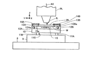
第1の実施形態で使用される露光装置を示す斜視図である。It is a perspective view which shows the exposure apparatus used in 1st Embodiment. 図1の露光装置のウエハ駆動機構を示す一部を切り欠いた図である。FIG. 2 is a partially cutaway view showing a wafer drive mechanism of the exposure apparatus of FIG. 1. 図2のウエハパック28を示す分解斜視図である。FIG. 3 is an exploded perspective view showing the wafer pack 28 of FIG. 2. 図2のウエハパック28の組立工程の一例を示す図である。FIG. 3 is a diagram illustrating an example of an assembly process of the wafer pack 28 of FIG. 2. 図5(A)は図2のウエハベース41上の磁性板62の磁化パターンの一例を示す平面図、図5(B)は磁性板62の磁化パターンの他の例の一部を示す図である。5A is a plan view showing an example of the magnetization pattern of the magnetic plate 62 on the wafer base 41 of FIG. 2, and FIG. 5B is a diagram showing a part of another example of the magnetization pattern of the magnetic plate 62. is there. 図6(A)はウエハをY方向に走査する場合のウエハパック28及びXYコイルキャリア40の動きの一例を示す平面図、図6(B)はウエハをX方向にステップ移動する場合のウエハパック28及びXYコイルキャリア40の動きの一例を示す平面図である。6A is a plan view showing an example of movement of the wafer pack 28 and the XY coil carrier 40 when the wafer is scanned in the Y direction, and FIG. 6B is a wafer pack when the wafer is stepped in the X direction. It is a top view which shows an example of a motion of 28 and XY coil carrier 40. FIG. 第1の実施形態のウエハ処理システムWTを示すブロック図である。1 is a block diagram showing a wafer processing system WT of a first embodiment. 第1の実施形態のウエハの処理方法の前半部を示すフローチャートである。It is a flowchart which shows the first half part of the processing method of the wafer of 1st Embodiment. 図8に続くウエハの処理方法を示すフローチャートである。FIG. 9 is a flowchart illustrating a wafer processing method following FIG. 8. FIG. 第1の実施形態のウエハパックの処理方法を示すフローチャートである。It is a flowchart which shows the processing method of the wafer pack of 1st Embodiment. ガラス板29とウエハWとの3つの分離方法の説明図である。It is explanatory drawing of three separation methods of the glass plate 29 and the wafer W. FIG. ガラス板29とウエハWとの別の3つの分離方法の説明図である。It is explanatory drawing of another three isolation | separation methods of the glass plate 29 and the wafer W. FIG. 第2の実施形態の露光装置の要部を示す一部を切り欠いた図である。It is the figure which notched the part which shows the principal part of the exposure apparatus of 2nd Embodiment.

符号の説明Explanation of symbols

R…レチクル、PL…投影光学系、W…ウエハ、21W…投影領域、28…ウエハパック、29…ガラス板、30…フレーム、33…ダイヤフラム、34…磁性板、35…緩衝部材、36A〜36C…Zアクチュエータ、37…静電軸受部材、64…第1平面モータ、72…第2平面モータ   R ... reticle, PL ... projection optical system, W ... wafer, 21W ... projection region, 28 ... wafer pack, 29 ... glass plate, 30 ... frame, 33 ... diaphragm, 34 ... magnetic plate, 35 ... buffer member, 36A-36C ... Z actuator, 37 ... electrostatic bearing member, 64 ... first planar motor, 72 ... second planar motor

[第1の実施形態]
以下、本発明の好ましい第1の実施形態につき図1〜図12を参照して説明する。本例は、スキャニング・ステッパよりなる走査露光型の露光装置(投影露光装置)を含むウエハ処理システム(図7参照)に本発明を適用したものである。先ず、その露光装置について説明する。
[First Embodiment]
Hereinafter, a preferred first embodiment of the present invention will be described with reference to FIGS. In this example, the present invention is applied to a wafer processing system (see FIG. 7) including a scanning exposure type exposure apparatus (projection exposure apparatus) comprising a scanning stepper. First, the exposure apparatus will be described.

図1は、本例の露光装置EXの概略構成を示す。図1において、露光装置EXは、露光光IL(露光ビーム)を用いて転写用のパターンが形成されたレチクルR(マスク)を照明する照明系20と、レチクルRを駆動するレチクルステージRSTと、レチクルRのパターンの像をウエハW(基板)上に投影する投影光学系PLと、ウエハWを駆動するウエハ駆動機構と、装置全体の動作を統括的に制御するコンピュータよりなる主制御系51と、その他の種々の制御又は演算等を行う処理系等とを備えている。露光光ILとして、本例ではArFエキシマレーザ光(波長193nm)が使用されている。なお、露光光としては、KrFエキシマレーザ光(波長248nm)、F2 レーザ光(波長157nm)などの紫外パルスレーザ光、YAGレーザの高調波、固体レーザ(半導体レーザなど)の高調波、又は水銀ランプの輝線(i線等)なども使用できる。FIG. 1 shows a schematic configuration of the exposure apparatus EX of this example. In FIG. 1, an exposure apparatus EX includes an illumination system 20 that illuminates a reticle R (mask) on which a transfer pattern is formed using exposure light IL (exposure beam), a reticle stage RST that drives the reticle R, A projection optical system PL that projects an image of the pattern of the reticle R onto a wafer W (substrate), a wafer drive mechanism that drives the wafer W, and a main control system 51 that includes a computer that comprehensively controls the operation of the entire apparatus; And a processing system for performing various other controls or calculations. In this example, ArF excimer laser light (wavelength 193 nm) is used as the exposure light IL. As the exposure light, ultraviolet pulsed laser light such as KrF excimer laser light (wavelength 248 nm), F 2 laser light (wavelength 157 nm), harmonics of YAG laser, harmonics of solid-state laser (semiconductor laser, etc.), or mercury Lamp bright lines (i-line etc.) can also be used.

照明系20は、例えば特開2001−313250号公報(対応する米国特許出願公開第2003/0025890号明細書)などに開示されるように、露光光源と、照明光学系とを含んでいる。照明光学系は、オプティカル・インテグレータ(フライアイレンズ、ロッドインテグレータ(内面反射型インテグレータ)、回折光学素子など)等を含む照度均一化光学系、及びレチクルブラインド等(いずれも不図示)を有する。照明系20は、レチクルブラインド(マスキングシステム)で規定されたレチクルR上のスリット状の照明領域21Rを露光光ILによりほぼ均一な照度分布で照明する。   The illumination system 20 includes an exposure light source and an illumination optical system as disclosed in, for example, Japanese Patent Application Laid-Open No. 2001-313250 (corresponding US Patent Application Publication No. 2003/0025890). The illumination optical system includes an illuminance uniformizing optical system including an optical integrator (a fly-eye lens, a rod integrator (an internal reflection type integrator), a diffractive optical element, etc.), a reticle blind, and the like (all not shown). The illumination system 20 illuminates the slit-shaped illumination region 21R on the reticle R defined by the reticle blind (masking system) with the exposure light IL with a substantially uniform illuminance distribution.

露光光ILのもとで、レチクルRの照明領域21R内のパターンは、両側テレセントリックの投影光学系PLを介して投影倍率β(βは例えば1/4,1/5等)で、ウエハW上の一つのショット領域上の非走査方向に細長い投影領域21W(図6(A)参照)に投影される。露光対象の基板としてのウエハWは、本例ではシリコン又はSOI(silicon on insulator)等の半導体からなる円板状の基材の表面にフォトレジスト(感光材料)を塗布したものである。また、そのウエハWを構成する円板状の基材の表面(露光面となる面)は研磨加工されて、極めて平面度の高い面とされている。この結果、ウエハWのフォトレジストが塗布されている表面も、極めて平面度の高い面である。一方、ウエハWを構成する円板状の基材の裏面、即ちウエハWの裏面の平面度は表面に比べて劣っている。   Under the exposure light IL, the pattern in the illumination area 21R of the reticle R is projected onto the wafer W at a projection magnification β (β is, for example, 1/4, 1/5, etc.) via the both-side telecentric projection optical system PL. Is projected onto a projection area 21W (see FIG. 6A) elongated in the non-scanning direction on one shot area. In this example, a wafer W as a substrate to be exposed is obtained by applying a photoresist (photosensitive material) to the surface of a disk-shaped substrate made of a semiconductor such as silicon or SOI (silicon on insulator). Further, the surface of the disk-shaped base material constituting the wafer W (the surface serving as the exposure surface) is polished to a surface with extremely high flatness. As a result, the surface of the wafer W on which the photoresist is applied is also a surface with extremely high flatness. On the other hand, the flatness of the back surface of the disk-shaped base material constituting the wafer W, that is, the back surface of the wafer W is inferior to that of the front surface.

本例の投影光学系PLは例えば屈折系であるが、反射屈折系等も使用できる。以下、図1において、投影光学系PLの光軸に平行にZ軸を取り、Z軸に垂直な平面内で走査露光時のレチクルR及びウエハWの走査方向に直交する非走査方向に沿ってX軸を取り、その走査方向に沿ってY軸を取って説明する。また、以下ではX軸、Y軸、Z軸に平行な方向をそれぞれX方向、Y方向、Z方向と呼び、X軸、Y軸、Z軸に平行な軸の周りの回転角(傾斜角)をそれぞれθX,θY,θZと呼ぶ。なお、本例では、X軸及びY軸に平行な面(XY平面)がほぼ水平面であり、−Z方向が鉛直下方である。   The projection optical system PL of this example is a refractive system, for example, but a catadioptric system or the like can also be used. Hereinafter, in FIG. 1, the Z-axis is taken in parallel to the optical axis of the projection optical system PL, and along a non-scanning direction orthogonal to the scanning direction of the reticle R and the wafer W during scanning exposure in a plane perpendicular to the Z-axis. A description will be given by taking the X axis and taking the Y axis along the scanning direction. In the following, the directions parallel to the X, Y, and Z axes are referred to as the X, Y, and Z directions, respectively, and the rotation angles (tilt angles) around the axes that are parallel to the X, Y, and Z axes. Are called θX, θY, and θZ, respectively. In this example, the plane parallel to the X axis and the Y axis (XY plane) is almost a horizontal plane, and the −Z direction is vertically downward.

先ず、レチクルRはレチクルステージRST上に吸着保持され、レチクルステージRSTはレチクルベース24上でY方向に一定速度で移動すると共に、例えば同期誤差(又はレチクルRのパターン像とウエハW上の露光中のショット領域との位置ずれ量)を補正するようにX方向、Y方向、及びZ軸周りの回転方向に微動して、レチクルRの走査を行う。レチクルステージRSTのX方向及びY方向の側面の反射面(又は移動鏡、コーナリフレクタ等)に対向するようにレーザ干渉計25X及び25Yが配置されている。レーザ干渉計25X及び25Yは、対応する反射面にレーザビーム(少なくとも一方は複数軸のレーザビーム)を照射することによって、例えば投影光学系PLを基準として少なくともレチクルステージRSTのX方向、Y方向の位置を分解能0.1nm程度で計測するとともに、回転角θZを計測し、計測値をステージ制御系53及び主制御系51に供給する。ステージ制御系53は、その計測値及び主制御系51からの制御情報に基づいて、不図示の駆動機構(リニアモータなど)を介してレチクルステージRSTの位置及び速度を制御する。   First, the reticle R is attracted and held on the reticle stage RST, and the reticle stage RST moves on the reticle base 24 at a constant speed in the Y direction. For example, a synchronization error (or a pattern image of the reticle R and the exposure on the wafer W is being exposed). The reticle R is scanned by finely moving in the X direction, the Y direction, and the rotational directions around the Z axis so as to correct the positional deviation amount from the shot area. Laser interferometers 25X and 25Y are arranged to face the reflecting surfaces (or moving mirrors, corner reflectors, etc.) on the side surfaces of reticle stage RST in the X direction and Y direction. The laser interferometers 25X and 25Y irradiate the corresponding reflecting surface with a laser beam (at least one of which is a multi-axis laser beam), for example, at least in the X direction and Y direction of the reticle stage RST with reference to the projection optical system PL. The position is measured with a resolution of about 0.1 nm, the rotation angle θZ is measured, and the measured value is supplied to the stage control system 53 and the main control system 51. The stage control system 53 controls the position and speed of the reticle stage RST via a drive mechanism (such as a linear motor) (not shown) based on the measurement value and the control information from the main control system 51.

また、レチクルRのパターン領域22をX方向に挟むように、アライメントマーク23A及び23Bが形成されている。レチクルRの上方には、光路折り曲げ用のミラーを介してアライメントマーク23A,23Bの位置を検出するためのレチクルアライメント顕微鏡26A,26Bが配置されている。レチクルアライメント顕微鏡26A,26Bの検出信号はアライメント信号処理系54に供給され、アライメント信号処理系54では画像処理方式等で検出したマーク位置の情報を主制御系51に供給する。   In addition, alignment marks 23A and 23B are formed so as to sandwich the pattern region 22 of the reticle R in the X direction. Above the reticle R, reticle alignment microscopes 26A and 26B for detecting the positions of the alignment marks 23A and 23B are arranged via optical path bending mirrors. Detection signals from the reticle alignment microscopes 26A and 26B are supplied to an alignment signal processing system 54. The alignment signal processing system 54 supplies information on mark positions detected by an image processing method or the like to the main control system 51.

また、投影光学系PLの鏡筒の下部周縁部に、ほぼ等角度間隔で3箇所にそれぞれZ方向に伸縮するZアクチュエータ36A,36B,36Cを介して環状の静電軸受部材37が設置され、静電軸受部材37にコンプレッサ38から可撓性を持つ配管39を介して露光光ILが通過する雰囲気中の気体(例えばドライエア、窒素、又はヘリウム等)と同じ種類の清浄で圧縮された気体が供給されている。そして、静電軸受部材37の底面側に所定間隔を隔てて、浅い箱状の容器であるウエハパック28内に収納されたウエハWが配置されている。ウエハパック28の上部は均一な厚さで矩形の平行平面板状のガラス板29で密閉され、ウエハWの表面(フォトレジストが塗布された露光面)の全面がガラス板29の投影光学系PLに対して反対側の面に密着するように、ウエハWはガラス板29側に付勢及び/又は吸着されている。   An annular electrostatic bearing member 37 is installed on the lower peripheral edge of the lens barrel of the projection optical system PL via Z actuators 36A, 36B, and 36C that extend and contract in the Z direction at approximately three equiangular intervals, respectively. A clean and compressed gas of the same type as the gas (for example, dry air, nitrogen, or helium) in the atmosphere through which the exposure light IL passes from the compressor 38 through the flexible pipe 39 to the electrostatic bearing member 37. Have been supplied. Wafers W housed in a wafer pack 28 which is a shallow box-like container are arranged at a predetermined interval on the bottom surface side of the electrostatic bearing member 37. The upper part of the wafer pack 28 is sealed with a rectangular parallel plane plate-like glass plate 29 having a uniform thickness, and the entire surface of the wafer W (exposure surface coated with a photoresist) is the projection optical system PL of the glass plate 29. The wafer W is biased and / or adsorbed on the glass plate 29 side so as to be in close contact with the opposite surface.

ガラス板29は、露光光ILを透過する石英又は蛍石(CaF2 )等の硝材から形成され、ガラス板29のウエハWの表面が密着している面及びこれと反対側の面の平面度は、ウエハWの表面の平面度と同等か、又はそれ以上に極めて高く加工され、ウエハWは露光光ILによってガラス板29を介して露光される。なお、投影光学系PLの先端部の光学部材とウエハWの表面との間の物体の屈折率が高い程、投影光学系PLの像の解像度を高くできるとともに、焦点深度を深くできるため、ガラス板29は露光光ILを透過するとともに、できるだけ露光光ILに対する屈折率の高い硝材から形成することが好ましい。The glass plate 29 is formed of a glass material such as quartz or fluorite (CaF 2 ) that transmits the exposure light IL, and the flatness of the surface of the glass plate 29 on which the surface of the wafer W is in close contact and the surface opposite thereto. Is processed to be equal to or higher than the flatness of the surface of the wafer W, and the wafer W is exposed through the glass plate 29 by the exposure light IL. Note that the higher the refractive index of the object between the optical member at the tip of the projection optical system PL and the surface of the wafer W, the higher the resolution of the image of the projection optical system PL and the greater the depth of focus. The plate 29 is preferably made of a glass material that transmits the exposure light IL and has a refractive index as high as possible with respect to the exposure light IL.

なお、ガラス板29の厚さは、ガラス板29が存在しないときの投影光学系PLとウエハWとの作動距離WD(投影光学系PLの先端部よりもウエハWに近い部材があるときには、この部材とウエハWとの距離)に、ほぼガラス板29の屈折率npを乗じて得られる光路長よりも所定のマージン分だけ薄いという条件下で、できるだけ厚いことが好ましい。その所定のマージンとは、後述のようにガラス板29及びウエハWを一体的にX方向、Y方向に駆動する際の、Z方向の位置の最大変動量である。一例として、ウエハWは厚さが0.75mm程度で、直径が200〜300mm程度の円板状であり、ガラス板29はそのウエハWの全面を覆うことができる矩形(正方形でもよい)で厚さが1mm程度の平板である。
なお、このようなガラス板29と略同様の機能を有しているのであれば、ガラス板29に代えて他の材料からなる部材を用いることも可能である。
The thickness of the glass plate 29 is such that the working distance WD between the projection optical system PL and the wafer W when the glass plate 29 is not present (when there is a member closer to the wafer W than the tip of the projection optical system PL). It is preferable that the thickness be as large as possible under the condition that the distance between the member and the wafer W is approximately a predetermined margin less than the optical path length obtained by multiplying the refractive index np of the glass plate 29. The predetermined margin is the maximum variation in the position in the Z direction when the glass plate 29 and the wafer W are integrally driven in the X direction and the Y direction as will be described later. As an example, the wafer W has a disk shape with a thickness of about 0.75 mm and a diameter of about 200 to 300 mm, and the glass plate 29 has a rectangular shape (which may be a square) that can cover the entire surface of the wafer W. Is a flat plate having a length of about 1 mm.
In addition, if it has a function substantially the same as such a glass plate 29, it can replace with the glass plate 29 and can also use the member which consists of another material.

図2は、図1の露光装置EXのウエハ駆動機構を示す一部を切り欠いた図である。図2において、Zアクチュエータ36Aは、静電軸受部材37に固定されたL字型の第1部材36A1と、この先端部を+Z方向に支持するように配置されて、Z方向に伸縮可能な電歪素子(ピエゾ素子等)又は磁歪素子等の駆動素子36A2と、この駆動素子36A2の底面と投影光学系PLの鏡筒とを連結するL字型の第2部材36A3とから構成されている。他のZアクチュエータ36B及び36Cも、それぞれ同様に駆動素子36B2及び36C2を備え、ステージ制御系53が駆動素子36A2〜36C2の伸縮量を制御して、静電軸受部材37の3箇所のZ方向の位置を制御することによって、投影光学系PLに対する静電軸受部材37のZ方向の位置、及び傾斜角θX,θYを微調整できる。   FIG. 2 is a partially cutaway view showing the wafer drive mechanism of the exposure apparatus EX of FIG. In FIG. 2, the Z actuator 36A includes an L-shaped first member 36A1 fixed to the electrostatic bearing member 37, and an electric electrode that is disposed so as to support the tip portion in the + Z direction and can expand and contract in the Z direction. The driving element 36A2 such as a distortion element (piezo element or the like) or a magnetostriction element, and an L-shaped second member 36A3 that connects the bottom surface of the driving element 36A2 and the lens barrel of the projection optical system PL. The other Z actuators 36B and 36C are similarly provided with drive elements 36B2 and 36C2, respectively, and the stage control system 53 controls the expansion / contraction amount of the drive elements 36A2 to 36C2, and the three Z-directions of the electrostatic bearing member 37 are arranged in the Z direction. By controlling the position, the position in the Z direction of the electrostatic bearing member 37 with respect to the projection optical system PL and the inclination angles θX and θY can be finely adjusted.

なお、図1の露光装置EXにおいて、レチクルベース24及び投影光学系PLは、一例として振動的に分離された不図示の異なるコラムに支持されている。そして、図2において、Zアクチュエータ36A〜36C中の投影光学系PLの鏡筒に固定されている第2部材(36A3等)を、投影光学系PLを支持しているコラムとは振動的に分離された別のコラムに固定してもよい。   In the exposure apparatus EX of FIG. 1, the reticle base 24 and the projection optical system PL are supported by different columns (not shown) that are separated in a vibrational manner as an example. In FIG. 2, the second member (36A3, etc.) fixed to the lens barrel of the projection optical system PL in the Z actuators 36A to 36C is vibrationally separated from the column supporting the projection optical system PL. It may be fixed to another column.

また、静電軸受部材37の底面側に環状の電極部材75が合成樹脂等の絶縁部材に埋め込まれて設置されている。電極部材75は、実際には、投影光学系PLの光軸AXの周りに等角度間隔で3分割され、分割された3個の電極部材75A,75B,75Cの電荷(又は相対的な電位)をステージ制御系53が独立に制御できるように構成されている。さらに、電極部材75を通して静電軸受部材37の底面(ウエハパック28のガラス板29に対向する面)にかけて、多数の吹き出し孔37aが形成され、これらの吹き出し孔37aは、静電軸受部材37の内部の通気孔37bに連通し、通気孔37bに配管39を介してコンプレッサ38が連結されている。この場合、ステージ制御系53が静電軸受部材37の電極部材75に電荷(例えば正電荷)を与えることによって、ガラス板29の上面に符号が逆の分極電荷(例えば負電荷)が生じて、ガラス板29は静電場によって静電軸受部材37側(+Z方向)に吸引される。また、ステージ制御系53がコンプレッサ38から静電軸受部材37の多数の吹き出し孔37aを介してガラス板29側に(−Z方向に)吹き出される気体の流量を制御することで、ガラス板29が静電軸受部材37に当接することが防止される。従って、ガラス板29を含むウエハパック28は、静電軸受部材37に対してエア予圧式の静電軸受方式によってZ方向に所定間隔を隔てて非接触状態で浮上するように保持される。   An annular electrode member 75 is embedded in an insulating member such as a synthetic resin on the bottom surface side of the electrostatic bearing member 37. The electrode member 75 is actually divided into three around the optical axis AX of the projection optical system PL at equal angular intervals, and the charges (or relative potentials) of the three divided electrode members 75A, 75B, and 75C. The stage control system 53 can be controlled independently. Further, a large number of blowing holes 37 a are formed through the electrode member 75 to the bottom surface of the electrostatic bearing member 37 (the surface facing the glass plate 29 of the wafer pack 28), and these blowing holes 37 a are formed on the electrostatic bearing member 37. The compressor 38 is connected to the vent hole 37b through a pipe 39. The compressor 38 is connected to the vent hole 37b. In this case, when the stage control system 53 gives an electric charge (for example, positive charge) to the electrode member 75 of the electrostatic bearing member 37, a polarization electric charge (for example, a negative electric charge) having a reverse sign is generated on the upper surface of the glass plate 29. The glass plate 29 is attracted to the electrostatic bearing member 37 side (+ Z direction) by an electrostatic field. Further, the stage control system 53 controls the flow rate of the gas blown from the compressor 38 to the glass plate 29 side (in the −Z direction) through the numerous blowout holes 37 a of the electrostatic bearing member 37. Is prevented from coming into contact with the electrostatic bearing member 37. Accordingly, the wafer pack 28 including the glass plate 29 is held against the electrostatic bearing member 37 so as to float in a non-contact state at a predetermined interval in the Z direction by an air preload electrostatic bearing system.

さらに、電極部材75は、実際には3つの電極部材75A〜75Cに分割されているため、ステージ制御系53はそれらの3つの電極部材75A〜75Cによるガラス板29に対する静電気による吸引力を個別に制御することによって、投影光学系PLに対するウエハパック28のZ方向の位置(フォーカス位置)、及び傾斜角θX,θY(レベリング)よりなる相対位置関係を調整する。個々の電極部材75A〜75Cによるウエハパック28のZ方向の駆動量は、例えば数nm〜数10nm程度である。このために、静電軸受部材37の内側のウエハW上の投影領域21W及び/又はこの近傍の領域の複数の計測点に所定パターンの像を投影する投光部61Aと、ウエハWで反射した検出光を受光する受光部61Bとを含み、その複数の計測点のZ方向の位置を検出するオートフォーカスセンサ(以下、AFセンサという。)61が設けられている。   Furthermore, since the electrode member 75 is actually divided into three electrode members 75A to 75C, the stage control system 53 individually applies the suction force due to static electricity to the glass plate 29 by the three electrode members 75A to 75C. By controlling, the relative positional relationship consisting of the position (focus position) of the wafer pack 28 in the Z direction with respect to the projection optical system PL and the tilt angles θX and θY (leveling) is adjusted. The driving amount of the wafer pack 28 in the Z direction by the individual electrode members 75A to 75C is, for example, about several nanometers to several tens of nanometers. For this purpose, the light projection unit 61A that projects an image of a predetermined pattern onto the projection area 21W on the wafer W inside the electrostatic bearing member 37 and / or a plurality of measurement points in the vicinity of the projection area 21W, and the light reflected by the wafer W. An autofocus sensor (hereinafter referred to as an AF sensor) 61 that includes a light receiving unit 61B that receives the detection light and detects the positions of the plurality of measurement points in the Z direction is provided.

なお、投光部61A及び受光部61Bは、それぞれ例えば検出光を折り曲げるミラー等の一部の光学系が静電軸受部材37の内側に配置されているのみで、その他の構成部材は、投影光学系PLの側面に配置されている。このAFセンサ61の計測値を処理することによって、ウエハWの表面の投影領域21Wの平均的な面のフォーカス位置及び傾斜角を求めることができ、これらの計測結果はステージ制御系53に供給される。なお、AFセンサ61としては、例えば特開平8−37149号公報に開示されているものを用いることができる。また、AFセンサ61は、ウエハWの表面の計測点の代わりに、ガラス板29の上面の計測点のZ方向の位置を計測し、この計測結果から既知のガラス板29の厚さを差し引くことで、間接的にウエハWの表面でのZ方向の位置を求めるようにしてもよい。   The light projecting unit 61A and the light receiving unit 61B are configured such that, for example, only a part of the optical system such as a mirror that bends the detection light is disposed inside the electrostatic bearing member 37. It is arranged on the side of the system PL. By processing the measurement values of the AF sensor 61, the focus position and the inclination angle of the average surface of the projection area 21W on the surface of the wafer W can be obtained, and these measurement results are supplied to the stage control system 53. The As the AF sensor 61, for example, one disclosed in JP-A-8-37149 can be used. The AF sensor 61 measures the position in the Z direction of the measurement point on the upper surface of the glass plate 29 instead of the measurement point on the surface of the wafer W, and subtracts the known thickness of the glass plate 29 from the measurement result. Thus, the position in the Z direction on the surface of the wafer W may be obtained indirectly.

この場合、一例として、予めテストプリント等によって、AFセンサ61によって計測される被検面のフォーカス位置及び傾斜角がそれぞれ0のときに、その被検面が投影光学系PLの像面に合致するようにAFセンサ61の初期のオフセット調整が行われている。そこで、ウエハWに対する露光時にステージ制御系53では、AFセンサ61によって計測されるウエハWの投影領域21Wのフォーカス位置及び傾斜角がそれぞれ0になるように、静電軸受部材37内の3個の電極部材75A〜75Cによるガラス板29に対する吸引力を制御する。これによって、ウエハWの表面が常に投影光学系PLの像面に合焦した状態で露光が行われる。   In this case, as an example, when the focus position and the tilt angle of the test surface measured by the AF sensor 61 are each 0 by test print or the like, the test surface matches the image plane of the projection optical system PL. Thus, the initial offset adjustment of the AF sensor 61 is performed. Therefore, in the stage control system 53 at the time of exposure to the wafer W, the three in the electrostatic bearing member 37 are set so that the focus position and the tilt angle of the projection area 21W of the wafer W measured by the AF sensor 61 become 0, respectively. The suction force with respect to the glass plate 29 by the electrode members 75A to 75C is controlled. As a result, exposure is performed with the surface of the wafer W always in focus on the image plane of the projection optical system PL.

さらに、例えばAFセンサ61の計測値に新たなオフセットが生じた場合には、そのオフセットを補正するように図1のZアクチュエータ36A〜36Cを駆動して、静電軸受部材37のフォーカス位置及び傾斜角を微調整してもよい。これによって、静電軸受部材37内の3個の電極部材75A〜75Cに対する制御が容易になる。なお、静電軸受部材37の吹き出し孔37aを等角度間隔で3組の吹き出し孔群に分割し、これらの3組の吹き出し孔群からウエハパック28に吹き出される気体の流量を独立に制御することによって、ウエハパック28のフォーカス位置及びレベリング角を制御してもよい。   Further, for example, when a new offset occurs in the measured value of the AF sensor 61, the Z actuators 36A to 36C in FIG. 1 are driven so as to correct the offset, and the focus position and inclination of the electrostatic bearing member 37 are corrected. The corner may be finely adjusted. This facilitates control of the three electrode members 75A to 75C in the electrostatic bearing member 37. The blowing holes 37a of the electrostatic bearing member 37 are divided into three sets of blowing hole groups at equal angular intervals, and the flow rate of the gas blown out from these three sets of blowing hole groups to the wafer pack 28 is independently controlled. Thus, the focus position and leveling angle of the wafer pack 28 may be controlled.

また、図2に示すように、ウエハパック28は、矩形の枠状の線膨張率が極めて小さい金属又はセラミックス等からなるフレーム30と、この上面に載置されるとともに、底面29aにウエハWの表面が密着しているガラス板29と、フレーム30の底面に溶接等によって固定されて、或る程度の可撓性を持つ非磁性体の金属製の薄い平板状のダイヤフラム33と、このダイヤフラム33の上面(ウエハWに対向する面)に固定されて、所定の磁化パターンが周期的に形成された矩形の平板状の磁性板34と、ウエハWの裏面と磁性板34の上面との間に介装された矩形(又はウエハWと同様の円形等でもよい)の平板状で少なくともZ方向に可撓性を持つ緩衝部材35とを備えている。緩衝部材35は、例えば合成ゴム又は合成樹脂(例えばフッ素系樹脂等)等から形成されて、磁性板34上に接着等によって固定されている。そして、ダイヤフラム33及び磁性板34側から緩衝部材35を介して、ウエハWがガラス板29側に付勢されている。   As shown in FIG. 2, the wafer pack 28 is mounted on a top surface of a frame 30 made of metal, ceramics, or the like having a rectangular frame-like linear expansion coefficient, and on the bottom surface 29a. A thin plate-like diaphragm 33 made of a non-magnetic metal plate fixed to the bottom surface of the frame 30 by welding or the like and having a certain degree of flexibility, and the diaphragm 33 A rectangular flat magnetic plate 34 fixed to the upper surface (the surface facing the wafer W) and having a predetermined magnetization pattern periodically formed between the back surface of the wafer W and the upper surface of the magnetic plate 34. A buffer member 35 having a rectangular shape (or a circular shape similar to the wafer W, etc.) and having flexibility in at least the Z direction is provided. The buffer member 35 is made of, for example, synthetic rubber or synthetic resin (for example, fluorine resin) and is fixed on the magnetic plate 34 by adhesion or the like. The wafer W is urged toward the glass plate 29 from the diaphragm 33 and the magnetic plate 34 via the buffer member 35.

さらに、図3は、図2のウエハパック28を示す分解斜視図である。図3に示すように、フレーム30の上面の周縁部にほぼ矩形の閉じた溝30aが形成され、この溝30a内に合成ゴム又は合成樹脂等の可撓性を持つオーリング32が装着されている。フレーム30の上面にガラス板29を載置すると、ガラス板29とフレーム30及びダイヤフラム33とで囲まれた空間(ウエハWが収納された空間)が、オーリング32によって気密化される。また、フレーム30の上面のオーリング32の内側からフレーム30の内面にかけて多数の吸着孔30cが形成されている。図2に示すように、フレーム30の−Y方向の側面には排気孔30dが形成され、排気孔30dに開閉用のバルブ31aを備えた排気管31が連結されている。この場合、予めバルブ31aを開いた状態で、排気管31を介してウエハパック28の内部が排気されて負圧にされ、ウエハWの表面は実質的に真空吸着によってもガラス板29の裏面29aに密着して保持される。この際に、フレーム30の多数の吸着孔30cを介してガラス板29はフレーム30に真空吸着されており、この状態でバルブ31aが閉じられている。なお、本例では、ウエハWは緩衝部材35によってもガラス板29側に付勢されているため、ウエハパック28内の真空度は、ガラス板29をフレーム30に安定に吸着できる程度であればよい。   Further, FIG. 3 is an exploded perspective view showing the wafer pack 28 of FIG. As shown in FIG. 3, a substantially rectangular closed groove 30a is formed at the periphery of the upper surface of the frame 30, and a flexible O-ring 32 such as synthetic rubber or synthetic resin is mounted in the groove 30a. Yes. When the glass plate 29 is placed on the upper surface of the frame 30, a space surrounded by the glass plate 29, the frame 30 and the diaphragm 33 (a space in which the wafer W is stored) is hermetically sealed by the O-ring 32. A number of suction holes 30 c are formed from the inside of the O-ring 32 on the upper surface of the frame 30 to the inner surface of the frame 30. As shown in FIG. 2, an exhaust hole 30d is formed on the side surface in the -Y direction of the frame 30, and an exhaust pipe 31 having an opening / closing valve 31a is connected to the exhaust hole 30d. In this case, with the valve 31a opened in advance, the inside of the wafer pack 28 is evacuated to a negative pressure through the exhaust pipe 31, and the surface of the wafer W is substantially back-surface 29a of the glass plate 29 by vacuum suction. It is held in close contact with. At this time, the glass plate 29 is vacuum-sucked to the frame 30 through the numerous suction holes 30c of the frame 30, and the valve 31a is closed in this state. In this example, since the wafer W is also urged to the glass plate 29 side by the buffer member 35, the degree of vacuum in the wafer pack 28 is as long as the glass plate 29 can be stably adsorbed to the frame 30. Good.

また、図3において、フレーム30の+X方向及び+Y方向の外側面は、互いに直交するとともに、レーザビームを反射できる高平面度の反射面に仕上げられている。なお、フレーム30の+X方向及び+Y方向の外側面に、レーザビームを反射するための薄い移動鏡を固定してもよい。さらに、フレーム30の±X方向の外側面には、複数箇所に小さい平板状の凸部30bが形成され、ウエハパック搬送用のアーム43によってそれらの凸部30bを介してフレーム30(ウエハパック28)を容易に搬送できるように構成されている。後述のようにウエハWをウエハパック28内に収納する工程では、一例としてフレーム30を反転する(ガラス板29が載置される面を鉛直下方にする)場合があるため、そのウエハパック搬送用のアーム43は、実際には凸部30bを上下に挟み込むように安定に保持する。そのアーム43によって、一例として、ウエハパック28は図1の露光装置EXの投影光学系PLの下方まで搬送される。   In FIG. 3, the outer surfaces of the frame 30 in the + X direction and the + Y direction are orthogonal to each other and finished to have a high flatness reflecting surface capable of reflecting the laser beam. A thin movable mirror for reflecting the laser beam may be fixed to the outer surface of the frame 30 in the + X direction and the + Y direction. Further, on the outer surface of the frame 30 in the ± X direction, small flat projections 30b are formed at a plurality of locations, and the frame 30 (wafer pack 28) is formed via the projections 30b by a wafer pack transfer arm 43. ) Can be transported easily. As will be described later, in the process of storing the wafer W in the wafer pack 28 as described later, the frame 30 may be reversed as an example (the surface on which the glass plate 29 is placed is vertically downward). In practice, the arm 43 stably holds the convex portion 30b so as to sandwich the convex portion 30b vertically. By way of example, the arm 43 transports the wafer pack 28 below the projection optical system PL of the exposure apparatus EX shown in FIG.

さらに、図3において、ウエハパック28の磁性板34には、一例としてX軸及びY軸に45°で交差するように放射状に磁化した4つのマグネット部MB1,MB2,MB3,MB4よりなる磁化ユニットMUBをX方向及びY方向にそれぞれ周期BX及びBYで2次元的に配置した磁化パターンが形成されている。実際には、その磁化パターンは、磁性板34の底面(ダイヤフラム33に接する面)側に所定の厚さで形成されている。なお、磁化ユニットMUBは、実際には垂直磁化(±Z方向に交互に磁化されていること)が好ましい。また、磁性板34を、マグネット部MB1〜MB4を単位とする独立の多数の永久磁石の集合体として構成してもよい。   Further, in FIG. 3, the magnetic plate 34 of the wafer pack 28 has, as an example, a magnetizing unit comprising four magnet portions MB1, MB2, MB3, MB4 that are radially magnetized so as to intersect the X axis and the Y axis at 45 °. Magnetization patterns are formed in which MUBs are two-dimensionally arranged in the X and Y directions with periods BX and BY, respectively. Actually, the magnetization pattern is formed with a predetermined thickness on the bottom surface (surface in contact with the diaphragm 33) side of the magnetic plate 34. In practice, the magnetization unit MUB is preferably perpendicularly magnetized (alternately magnetized in the ± Z directions). Moreover, you may comprise the magnetic board 34 as an aggregate | assembly of many independent permanent magnets which make magnet part MB1-MB4 a unit.

磁性板34の材料は、例えばコバルト系、ニッケル系、又はネオジウム鉄ボロン系等の強磁性体である。さらに、磁性板34は、本例の露光装置EXが設置される室温(例えば23°C)下で線膨張率が極めて小さい磁性材料、好ましくは線膨張率がほぼ0の磁性材料から形成される。線膨張率がほぼ0の材料としては、例えばスーパーインバーマグネットが挙げられる。これによって、後述のように磁力によって磁性板34(ウエハパック28)を駆動する際に、磁性板34の温度が或る程度上昇しても、ウエハパック28及びその内部のウエハWに歪が生じることがない。   The material of the magnetic plate 34 is a ferromagnetic material such as cobalt, nickel, or neodymium iron boron. Further, the magnetic plate 34 is formed of a magnetic material having an extremely small linear expansion coefficient at room temperature (for example, 23 ° C.) where the exposure apparatus EX of the present example is installed, preferably a magnetic material having a linear expansion coefficient of approximately zero. . An example of a material having a linear expansion coefficient of approximately zero is a super invar magnet. As a result, when the magnetic plate 34 (wafer pack 28) is driven by magnetic force as will be described later, even if the temperature of the magnetic plate 34 rises to some extent, the wafer pack 28 and the wafer W inside thereof are distorted. There is nothing.

ここで、例えば露光装置EXに近接して配置される作業領域で、未露光のウエハWをウエハパック28内に収納する工程の一例につき、図4を参照して説明する。
先ず、図4(A)に示すように、ガラス板29は反転されてその底面29a(ウエハWが当接する面)が鉛直上方(+Z方向)を向くように、支持部材44上に真空吸着又は静電吸着によって保持されている。次に、ウエハ搬送アーム45の先端部にウエハWの裏面が真空吸着等によって保持された状態で、ウエハWの表面Waがガラス板29の底面29aに対向した後、ウエハ搬送アーム45を降下させる。そして、図4(B)に示すように、ウエハWの表面がガラス板29の底面29aに当接した後、ウエハ搬送アーム45の真空吸着を解除して、ウエハ搬送アーム45を待避させる。
Here, an example of a process of storing the unexposed wafer W in the wafer pack 28 in a work area arranged close to the exposure apparatus EX will be described with reference to FIG.
First, as shown in FIG. 4 (A), the glass plate 29 is inverted and is vacuum-adsorbed on the support member 44 so that its bottom surface 29a (surface on which the wafer W abuts) faces vertically upward (+ Z direction). It is held by electrostatic adsorption. Next, the wafer transfer arm 45 is lowered after the front surface Wa of the wafer W faces the bottom surface 29a of the glass plate 29 with the back surface of the wafer W held by vacuum suction or the like at the tip of the wafer transfer arm 45. . 4B, after the surface of the wafer W comes into contact with the bottom surface 29a of the glass plate 29, the vacuum suction of the wafer transfer arm 45 is released, and the wafer transfer arm 45 is retracted.

その後、図4(C)に示すように、ダイヤフラム33、磁性板34、緩衝部材35、及びオーリング32が装着されたフレーム30を、ウエハパック搬送用のアーム(不図示)によって反転させた状態でウエハWの裏面上に搬送した後、そのアームを降下させて、図4(D)に示すように、フレーム30をガラス板29の底面に載置する。この状態で、主にフレーム30及び磁性板34の荷重によって、緩衝部材35を介してウエハWはガラス板29側に付勢されており、ウエハWの表面はほぼガラス板29の底面に密着している。そして、フレーム30の排気管31のバルブ31aを開いて、排気管31に可撓性を持つ配管46aを介して真空ポンプ46を連結し、真空ポンプ46によって排気孔30dを通してフレーム30、ダイヤフラム33、及びガラス板29で囲まれた空間内の気体を排気する。この結果、吸着孔30cを介してガラス板29がフレーム30に吸着されるとともに、ウエハWの表面のガラス板29の底面に対する密着度が高められる。この状態で、バルブ31aを閉じて、配管46aを排気管31から取り外すことによって、ウエハパック28内へのウエハWの収納が完了する。その後、ウエハパック搬送用のアームによってウエハパック28は反転されて、図1の露光装置EX側に搬送される。   Thereafter, as shown in FIG. 4C, the frame 30 on which the diaphragm 33, the magnetic plate 34, the buffer member 35, and the O-ring 32 are mounted is inverted by a wafer pack transfer arm (not shown). Then, the arm 30 is lowered and the frame 30 is placed on the bottom surface of the glass plate 29 as shown in FIG. In this state, the wafer W is biased toward the glass plate 29 via the buffer member 35 mainly by the load of the frame 30 and the magnetic plate 34, and the surface of the wafer W is in close contact with the bottom surface of the glass plate 29. ing. Then, the valve 31a of the exhaust pipe 31 of the frame 30 is opened, and the vacuum pump 46 is connected to the exhaust pipe 31 through a flexible pipe 46a. The vacuum pump 46 allows the frame 30, the diaphragm 33, And the gas in the space surrounded by the glass plate 29 is exhausted. As a result, the glass plate 29 is attracted to the frame 30 through the suction holes 30c, and the degree of adhesion of the surface of the wafer W to the bottom surface of the glass plate 29 is increased. In this state, the valve 31a is closed and the piping 46a is removed from the exhaust pipe 31, whereby the wafer W is completely stored in the wafer pack 28. Thereafter, the wafer pack 28 is reversed by the wafer pack transfer arm and transferred to the exposure apparatus EX side in FIG.

なお、ガラス板29とウエハWの表面との間に気泡等が残されるのを防止するために、ガラス板29にウエハWの表面を密着させる工程は、例えば高真空に設定されたチャンバ内で行ってもよい。さらに、図4(A)〜図4(D)までの作業を所定の負圧に設定されたチャンバ内で行うようにしてもよい。この場合には、排気管31のバルブ31aを閉じたままにしておくことで、フレーム30、ダイヤフラム33、及びガラス板29で囲まれた空間は、作業完了時には自動的にその負圧に設定される。   In order to prevent bubbles and the like from being left between the glass plate 29 and the surface of the wafer W, the step of bringing the surface of the wafer W into close contact with the glass plate 29 is performed, for example, in a chamber set to a high vacuum. You may go. Furthermore, the operations from FIG. 4A to FIG. 4D may be performed in a chamber set at a predetermined negative pressure. In this case, by keeping the valve 31a of the exhaust pipe 31 closed, the space surrounded by the frame 30, the diaphragm 33, and the glass plate 29 is automatically set to the negative pressure when the work is completed. The

次に、露光装置EXによって露光が行われたウエハWをウエハパック28から取り出す場合には、図4(D)の状態で(ただし、排気管31に真空ポンプ46を連結する必要はない)、バルブ31aを開いてウエハパック28の内部を大気に開放した後、図4(C)に示すように、フレーム30を上昇させる。次に、図4(B)に示すように、ガラス板29を支持部材44側に吸着保持した状態で、ウエハ搬送アーム45によってウエハWの裏面を吸着して、ウエハ搬送アーム45を上昇させることで、露光済みのウエハWを取り出すことができる。取り出されたウエハWは、例えばコータ・デベロッパに搬送されてフォトレジストの現像が行われる。   Next, when the wafer W exposed by the exposure apparatus EX is taken out from the wafer pack 28, in the state of FIG. 4D (however, it is not necessary to connect the vacuum pump 46 to the exhaust pipe 31). After opening the valve 31a to open the interior of the wafer pack 28 to the atmosphere, the frame 30 is raised as shown in FIG. Next, as shown in FIG. 4B, the wafer transfer arm 45 is lifted by sucking the back surface of the wafer W by the wafer transfer arm 45 in a state where the glass plate 29 is sucked and held on the support member 44 side. Thus, the exposed wafer W can be taken out. The taken out wafer W is transported to a coater / developer, for example, and development of the photoresist is performed.

なお、ガラス板29とウエハW(フォトレジスト層)とが密着していて、簡単には離れないような場合に、ガラス板29とウエハWとを分離する手法については後述する。
なお、図3のウエハパック28では、フレーム30にダイヤフラム33が固定されており、ガラス板29はフレーム30に着脱自在であるが、逆に、フレーム30にガラス板29を固定して、ダイヤフラム33をフレーム30に着脱自在としてもよい。
A method for separating the glass plate 29 and the wafer W when the glass plate 29 and the wafer W (photoresist layer) are in close contact and cannot be separated easily will be described later.
3, the diaphragm 33 is fixed to the frame 30, and the glass plate 29 is detachable from the frame 30, but conversely, the glass plate 29 is fixed to the frame 30 and the diaphragm 33 is fixed. May be detachable from the frame 30.

図1に戻り、ウエハパック28の下方に矩形の平板状で駆動用の種々のコイル等が設けられたXYコイルキャリア40が配置され、XYコイルキャリア40は、気体軸受方式によって非接触状態で、平板状のウエハベース41上にX方向、Y方向、及びZ軸の周りの回転方向に移動可能に載置されている。XYコイルキャリア40の底面側には、ウエハベース41に対してXYコイルキャリア40をX方向、Y方向に駆動するとともに回転角θZを制御する第1平面モータ64用の駆動コイルが設置され、XYコイルキャリア40の上面側には、XYコイルキャリア40に対してウエハパック28(図3の磁性板34)をX方向、Y方向に駆動するとともに回転角θZを制御する第2平面モータ72用の駆動コイルが設置されている。   Returning to FIG. 1, an XY coil carrier 40 is disposed below the wafer pack 28 in a rectangular flat plate shape and provided with various coils for driving. The XY coil carrier 40 is in a non-contact state by a gas bearing system, It is mounted on a flat wafer base 41 so as to be movable in the X direction, the Y direction, and the rotational direction around the Z axis. On the bottom surface side of the XY coil carrier 40, a drive coil for the first planar motor 64 that drives the XY coil carrier 40 in the X and Y directions with respect to the wafer base 41 and controls the rotation angle θZ is installed. On the upper surface side of the coil carrier 40, the wafer pack 28 (the magnetic plate 34 in FIG. 3) is driven in the X and Y directions with respect to the XY coil carrier 40, and the second planar motor 72 for controlling the rotation angle θZ is controlled. A drive coil is installed.

また、ウエハパック28(フレーム30)の+X方向及び+Y方向の側面の反射面(又は移動鏡)に対向するようにレーザ干渉計42X及び42Yが配置されている。レーザ干渉計42A及び42Yは、対応する反射面にレーザビーム(少なくとも一方は複数軸のレーザビーム)を照射することによって、例えば投影光学系PLを基準として、少なくともウエハパック28のX方向、Y方向の位置を分解能0.1nm程度で計測するとともに、回転角θZを計測し、計測値をステージ制御系53及び主制御系51に供給する。さらに、本例では、後述のように、XYコイルキャリア40に対するウエハパック28のX方向、Y方向の相対位置を分解能10μm程度で計測するとともに、回転角θZを計測するためのリニアエンコーダと、ウエハベース41に対するXYコイルキャリア40のX方向、Y方向の相対位置を分解能10μm程度で計測するとともに、回転角θZを計測するためのリニアエンコーダとが備えられている。これらのリニアエンコーダの計測値もステージ制御系53に供給されている。ステージ制御系53は、レーザ干渉計42X,42Y及びそれらのリニアエンコーダの計測値、並びに主制御系51からの制御情報に基づいて、上記の平面モータ64及び72を介してウエハパック28及びXYコイルキャリア40の位置及び速度を制御する。   Laser interferometers 42X and 42Y are arranged so as to face the reflecting surfaces (or movable mirrors) on the side surfaces of the wafer pack 28 (frame 30) in the + X direction and the + Y direction. The laser interferometers 42A and 42Y irradiate the corresponding reflecting surface with a laser beam (at least one of which is a multi-axis laser beam), for example, with reference to the projection optical system PL, at least the X direction and Y direction of the wafer pack 28 Is measured with a resolution of about 0.1 nm, the rotation angle θZ is measured, and the measured value is supplied to the stage control system 53 and the main control system 51. Furthermore, in this example, as will be described later, the relative position of the wafer pack 28 in the X and Y directions with respect to the XY coil carrier 40 is measured with a resolution of about 10 μm, and a linear encoder for measuring the rotation angle θZ, and the wafer A linear encoder for measuring the relative position of the XY coil carrier 40 with respect to the base 41 in the X direction and the Y direction with a resolution of about 10 μm and for measuring the rotation angle θZ is provided. The measurement values of these linear encoders are also supplied to the stage control system 53. The stage control system 53 receives the wafer pack 28 and the XY coil via the planar motors 64 and 72 based on the measurement values of the laser interferometers 42X and 42Y and their linear encoders and the control information from the main control system 51. The position and speed of the carrier 40 are controlled.

また、投影光学系PLの+Y方向の側面には、ウエハW上のアライメントマーク(ウエハマーク)の位置を検出するためのオフ・アクシス方式で撮像方式のアライメントセンサALGが配置されており、アライメントセンサALGの検出信号はアライメント信号処理系54に供給されている。アライメント信号処理系54は、その検出信号に基づいて例えばエンハンスド・グローバル・アライメント方式(EGA方式)でウエハW上の全部のショット領域の配列情報を求めて主制御系51に供給する。この場合、予めレチクルRのパターンの投影光学系PLを介した像の基準位置(アライメントマーク23A,23Bの像の中心等)と、アライメントセンサALGの検出位置との位置関係(ベースライン量等)の情報が計測されて、記憶されている。そのために、図3に示すように、ウエハパック28のガラス板29の底面のウエハWの近傍には、基準マークFM1等が形成されている。   Further, on the side surface in the + Y direction of the projection optical system PL, an off-axis imaging type alignment sensor ALG for detecting the position of the alignment mark (wafer mark) on the wafer W is arranged. An ALG detection signal is supplied to an alignment signal processing system 54. The alignment signal processing system 54 obtains the array information of all shot areas on the wafer W by the enhanced global alignment method (EGA method) based on the detection signal and supplies it to the main control system 51. In this case, the positional relationship (baseline amount, etc.) between the reference position of the image of the pattern of the reticle R in advance through the projection optical system PL (center of the image of the alignment marks 23A, 23B, etc.) and the detection position of the alignment sensor ALG. Is measured and stored. Therefore, as shown in FIG. 3, a reference mark FM1 and the like are formed in the vicinity of the wafer W on the bottom surface of the glass plate 29 of the wafer pack 28.

また、本例の露光装置EXは、投影光学系PLの先端の光学部材とウエハW上のガラス板29との間の局所的な領域(液浸領域)に純水等の液体を供給し、露光光ILで投影光学系PL、液体、及びガラス板29を介してウエハWを露光する液浸方式であることが好ましい。この場合、その液浸領域の広がりを抑制するために、ガラス板29の上面にその液体に対して撥液性のコーティングを施すことが好ましい。このように液浸方式とすることによって、その液体及びガラス板29の屈折率に応じて投影光学系PLの解像度及び焦点深度を向上できる。従って、その液体としては、露光光ILを透過するとともに、できるだけ屈折率の大きい液体(例えばデカリン(decalin)等)が好ましい。液浸法で露光するためには、例えば国際公開第99/49504号パンフレット又は国際公開第2005/122221号パンフレット等に開示されているように、かつ図2に示すように、その液浸領域に配管48a及びノズルを介して液体LQを供給する液体供給装置48と、その液浸領域の液体LQをノズル及び配管49aを介して回収する液体回収装置49とを設ければよい。   Further, the exposure apparatus EX of this example supplies a liquid such as pure water to a local region (immersion region) between the optical member at the tip of the projection optical system PL and the glass plate 29 on the wafer W, A liquid immersion method is preferred in which the wafer W is exposed with the exposure light IL through the projection optical system PL, the liquid, and the glass plate 29. In this case, in order to suppress the spread of the liquid immersion region, it is preferable to apply a liquid repellent coating to the liquid on the upper surface of the glass plate 29. By adopting the immersion method in this way, the resolution and depth of focus of the projection optical system PL can be improved according to the liquid and the refractive index of the glass plate 29. Accordingly, the liquid is preferably a liquid that transmits the exposure light IL and has a refractive index as large as possible (for example, decalin). In order to perform exposure by the immersion method, for example, as disclosed in WO99 / 49504 or WO2005 / 122221, and as shown in FIG. What is necessary is just to provide the liquid supply apparatus 48 which supplies the liquid LQ via the piping 48a and a nozzle, and the liquid collection | recovery apparatus 49 which collect | recovers the liquid LQ of the liquid immersion area | region via a nozzle and the piping 49a.

図1の露光装置EXを用いた露光時には、不図示のウエハローダ系によって、未露光のウエハWを収納したウエハパック28がXYコイルキャリア40上に載置された後、レチクルR及びウエハWのアライメントが行われる。その後、静電軸受部材37を介してウエハパック28を非接触に浮上させて保持した状態で、照明光学系20から露光光ILをレチクルR上の照明領域21Rに照射する。そして、照明領域21R内のパターンを投影光学系PLを介してウエハW上の一つのショット領域上の投影領域に投影した状態で、レチクルステージRST及びXYコイルキャリア40の平面モータを駆動して、レチクルRとウエハW(ウエハパック28)とをY方向に同期移動する動作と、露光光ILの照射を停止して、XYコイルキャリア40の平面モータを駆動してウエハW(ウエハパック28)をX方向及び/又はY方向にステップ移動する動作とが繰り返される。この動作の繰り返しによって、ステップ・アンド・スキャン方式でウエハW上の各ショット領域にレチクルRのパターン像が露光される。その後、不図示のウエハローダ系によって、露光済みのウエハWを収納したウエハパック28は、コータ・デベロッパ(不図示)側に搬送される。   At the time of exposure using the exposure apparatus EX of FIG. 1, the wafer pack 28 containing the unexposed wafer W is placed on the XY coil carrier 40 by a wafer loader system (not shown), and then the alignment of the reticle R and the wafer W is performed. Is done. Thereafter, the illumination light 21 is irradiated from the illumination optical system 20 onto the illumination region 21R on the reticle R in a state where the wafer pack 28 is lifted and held in a non-contact manner via the electrostatic bearing member 37. Then, in a state where the pattern in the illumination area 21R is projected onto the projection area on one shot area on the wafer W via the projection optical system PL, the plane motors of the reticle stage RST and the XY coil carrier 40 are driven, The operation of synchronously moving the reticle R and the wafer W (wafer pack 28) in the Y direction and the irradiation of the exposure light IL are stopped, and the planar motor of the XY coil carrier 40 is driven to move the wafer W (wafer pack 28). The operation of stepping in the X direction and / or the Y direction is repeated. By repeating this operation, the pattern image of the reticle R is exposed to each shot area on the wafer W by the step-and-scan method. Thereafter, the wafer pack 28 containing the exposed wafer W is transferred to a coater / developer (not shown) by a wafer loader system (not shown).

次に、本例の図1の露光装置EXのXYコイルキャリア40及びウエハパック28を駆動するための平面モータ64及び72の構成等、並びにウエハパック28及びウエハベース41とXYコイルキャリア40との2次元的な相対位置を計測するためのリニアエンコーダの構成等につき説明する。
図2に示すように、露光装置EXのウエハベース41は床FL上に設置され、ウエハベース41の上面には、所定の磁化パターンが周期的に形成された磁性板62が固定されている。磁性板62の上面は高い平面度に仕上げられており、磁性板62上に、気体を吹き出す複数(例えば4隅)のエアガイド68を介して非接触状態で、XYコイルキャリア40が載置されている。XYコイルキャリア40の底面に第1平面モータ64を構成するX軸の駆動コイル63X及びY軸の駆動コイル63Yが固定されている。
Next, the configuration of the planar motors 64 and 72 for driving the XY coil carrier 40 and the wafer pack 28 of the exposure apparatus EX of FIG. 1 of this example, and the wafer pack 28 and the wafer base 41 and the XY coil carrier 40 are arranged. A configuration of a linear encoder for measuring a two-dimensional relative position will be described.
As shown in FIG. 2, the wafer base 41 of the exposure apparatus EX is installed on the floor FL, and a magnetic plate 62 on which a predetermined magnetization pattern is periodically formed is fixed on the upper surface of the wafer base 41. The upper surface of the magnetic plate 62 is finished with high flatness, and the XY coil carrier 40 is placed on the magnetic plate 62 in a non-contact state via a plurality of (for example, four corners) air guides 68 for blowing out gas. ing. An X-axis drive coil 63X and a Y-axis drive coil 63Y constituting the first planar motor 64 are fixed to the bottom surface of the XY coil carrier 40.

図5(A)は、図1のウエハベース41を示す平面図である。図5(A)において、磁性板62の表面には所定の厚さで、X軸及びY軸に45°で交差するように放射状に磁化した4つのマグネット部MA1,MA2,MA3,MA4よりなる磁化ユニットMUAをX方向及びY方向にそれぞれ周期AX及びAYで2次元的に配置した磁化パターンが形成されている。このように、表面に磁化パターンが形成された磁性板62を用いることによって、その上の2点鎖線で示すXYコイルキャリア40を第1平面モータ64で駆動する際に、より重心に近い位置での駆動が可能になり、XYコイルキャリア40をより安定に駆動できる。   FIG. 5A is a plan view showing the wafer base 41 of FIG. In FIG. 5A, the surface of the magnetic plate 62 is composed of four magnet portions MA1, MA2, MA3, MA4 having a predetermined thickness and radially magnetized so as to intersect the X axis and the Y axis at 45 °. A magnetization pattern is formed in which the magnetization units MUA are two-dimensionally arranged in the X and Y directions with periods AX and AY, respectively. In this way, by using the magnetic plate 62 having the magnetization pattern formed on the surface, when the XY coil carrier 40 indicated by the two-dot chain line on the surface is driven by the first planar motor 64, the position is closer to the center of gravity. XY coil carrier 40 can be driven more stably.

なお、磁化ユニットMUAを用いる代わりに、図5(B)に示すように、+Z方向に磁化したマグネット部MC1,MC3と、−Z方向に磁化したマグネット部MC2,MC4とからなる垂直磁化した磁化ユニットMUCをX軸及びY軸に45°で交差する方向に所定ピッチで配列した磁化パターンを用いることが好ましい。また、磁性板62を、マグネット部MA1〜MA4を単位とする個別の多数の永久磁石の集合体として構成してもよい。磁性板62は、ウエハパック28内の磁性板34と同様に、本例の露光装置EXが設置される室温下で線膨張率が極めて小さい磁性材料、好ましくはスーパーインバーマグネット等のように線膨張率がほぼ0の磁性材料から形成される。これによって、磁性板62に対して磁力によってXYコイルキャリア40を駆動する際に、磁性板62の温度が或る程度上昇しても、ウエハベース41に歪が生じることがなく、XYコイルキャリア40を高精度に駆動できる。   Instead of using the magnetization unit MUA, as shown in FIG. 5 (B), the perpendicularly magnetized magnetization comprising the magnet parts MC1 and MC3 magnetized in the + Z direction and the magnet parts MC2 and MC4 magnetized in the −Z direction. It is preferable to use a magnetization pattern in which the units MUC are arranged at a predetermined pitch in a direction crossing the X axis and the Y axis at 45 °. The magnetic plate 62 may be configured as an assembly of a large number of individual permanent magnets having the magnet portions MA1 to MA4 as a unit. Similar to the magnetic plate 34 in the wafer pack 28, the magnetic plate 62 is a magnetic material having a very low linear expansion coefficient at room temperature where the exposure apparatus EX of this example is installed, preferably linear expansion such as a super invar magnet. It is formed from a magnetic material with a rate of approximately zero. As a result, when the XY coil carrier 40 is driven by the magnetic force with respect to the magnetic plate 62, the wafer base 41 is not distorted even if the temperature of the magnetic plate 62 rises to some extent, and the XY coil carrier 40. Can be driven with high accuracy.

また、図5(A)において、XYコイルキャリア40の底面には、磁性板62の磁化パターンの周期に応じて、XYコイルキャリア40をX方向(非走査方向)に駆動するための例えば3相のX軸の駆動コイル63Xと、XYコイルキャリア40をY方向(走査方向SD)に駆動するための例えば3相のY軸の駆動コイル63Yとが、それぞれ複数組設置されている。この場合、駆動コイル63X及び63Yと、磁性板62の磁化パターン(より正確にはX方向及びY方向に周期AX及びAYで変化する磁場分布)とから、それぞれX軸のリニアモータ64X及びY軸のリニアモータ64Yが構成され、2軸のリニアモータ64X及び64Yから第1平面モータ64が構成されている(図2参照)。ステージ制御系53の制御のもとで、リニアモータ64X及び64Yはそれぞれウエハベース41に対してXYコイルキャリア40をX方向及びY方向に非接触状態で駆動する。また、図5(A)から分かるように、リニアモータ64X及び64Yはそれぞれ複数軸であるため、一方のリニアモータ64X(又は64Y)を2軸で異なる駆動量だけ駆動することによって、XYコイルキャリア40の回転角θZを制御することも可能である。なお、平面モータ64を使用する代わりに、駆動方向が直交する2つの1次元のリニアモータ等を組み合わせた駆動機構を用いてもよい。   5A, on the bottom surface of the XY coil carrier 40, for example, three phases for driving the XY coil carrier 40 in the X direction (non-scanning direction) according to the period of the magnetization pattern of the magnetic plate 62. A plurality of sets of X-axis drive coils 63X and, for example, three-phase Y-axis drive coils 63Y for driving the XY coil carrier 40 in the Y direction (scanning direction SD) are provided. In this case, the X-axis linear motors 64X and Y-axis are respectively determined from the drive coils 63X and 63Y and the magnetization pattern of the magnetic plate 62 (more precisely, the magnetic field distribution changing with the periods AX and AY in the X and Y directions). The linear motor 64Y is configured, and the first planar motor 64 is configured by the biaxial linear motors 64X and 64Y (see FIG. 2). Under the control of the stage control system 53, the linear motors 64X and 64Y drive the XY coil carrier 40 with respect to the wafer base 41 in a non-contact state in the X direction and the Y direction, respectively. Further, as can be seen from FIG. 5A, since the linear motors 64X and 64Y each have a plurality of axes, the XY coil carrier can be obtained by driving one linear motor 64X (or 64Y) by different driving amounts on the two axes. It is also possible to control the rotation angle θZ of 40. Instead of using the planar motor 64, a driving mechanism in which two one-dimensional linear motors whose driving directions are orthogonal to each other may be used.

また、XYコイルキャリア40の底面に、ウエハベース41上の磁性板62の磁化パターンの磁場(X方向、Y方向に周期AX,AYで変化する磁場)を検出するホール素子等を含む検出器67A及び67Bが固定されている。検出器67A及び67Bはそれぞれウエハベース41(磁性板62)に対するXYコイルキャリア40のX方向、Y方向の相対位置を分解能10μm程度で検出する。これらの検出結果からXYコイルキャリア40の回転角θZも求められる。検出器67A及び67Bの検出結果は、X軸及びY軸の駆動コイル63X及び63Yの相切り換え(コミュテーション)にも使用される。   The detector 67A includes a Hall element or the like that detects a magnetic field (a magnetic field that changes in the X and Y directions with a period AX and AY) on the bottom surface of the XY coil carrier 40 on the magnetic plate 62 on the wafer base 41. And 67B are fixed. The detectors 67A and 67B detect relative positions in the X direction and Y direction of the XY coil carrier 40 with respect to the wafer base 41 (magnetic plate 62) with a resolution of about 10 μm. The rotation angle θZ of the XY coil carrier 40 is also obtained from these detection results. The detection results of the detectors 67A and 67B are also used for phase switching (commutation) of the X-axis and Y-axis drive coils 63X and 63Y.

なお、検出器67A及び67Bはインクリメンタル方式であるため、原点を設定するために、磁性板62の+Y方向の端部に、X方向に所定間隔で原点検出用のパターン65A及び65Bが埋め込まれている。これに対応して、XYコイルキャリア40の底面の+Y方向の端部には、パターン65A及び65Bと同じX方向の間隔で、パターン65A及び65BのX方向、Y方向の絶対位置を磁性板62の磁化パターンの周期AX,AYよりも狭い範囲内で検出するための、光学式又は静電容量式等の原点センサ66A及び66Bが固定されている。本例では、一例として、原点センサ66A及び66Bで同時にパターン65A及び65BのX方向、Y方向の位置を検出してから、検出器67A,67Bで検出される磁場が所定位相になるときに、検出器67A及び67BのX軸、Y軸の計測値をそれぞれリセットする。この後に検出器67A及び67Bによって検出されるXYコイルキャリア40の位置は、ウエハベース41上のパターン65A及び65Bを基準とする絶対位置とみなすことが可能である。このように、パターン65A,65B、原点センサ66A,66B、磁性板62の磁化パターン、及び検出器67A,67Bを含んで、ウエハベース41に対するXYコイルキャリア40の2次元的な相対位置を計測するための第1リニアエンコーダが構成されている。この第1リニアエンコーダの計測値はステージ制御系53に供給されている。   Since the detectors 67A and 67B are an incremental method, the origin detection patterns 65A and 65B are embedded at predetermined intervals in the X direction at the end portion in the + Y direction of the magnetic plate 62 in order to set the origin. Yes. Correspondingly, the absolute positions of the patterns 65A and 65B in the X and Y directions are set at the end of the bottom surface of the XY coil carrier 40 in the + Y direction at the same interval in the X direction as the patterns 65A and 65B. The origin sensors 66A and 66B such as an optical type or a capacitance type are fixed for detection within a range narrower than the periods AX and AY of the magnetization patterns. In this example, as an example, when the origin sensors 66A and 66B simultaneously detect the positions of the patterns 65A and 65B in the X direction and the Y direction, the magnetic fields detected by the detectors 67A and 67B become a predetermined phase. The X axis and Y axis measurement values of the detectors 67A and 67B are reset. Thereafter, the position of the XY coil carrier 40 detected by the detectors 67A and 67B can be regarded as an absolute position based on the patterns 65A and 65B on the wafer base 41. As described above, the two-dimensional relative position of the XY coil carrier 40 with respect to the wafer base 41 is measured including the patterns 65A and 65B, the origin sensors 66A and 66B, the magnetization pattern of the magnetic plate 62, and the detectors 67A and 67B. For this purpose, a first linear encoder is configured. The measurement value of the first linear encoder is supplied to the stage control system 53.

また、図6(A)は、図2のウエハパック28、XYコイルキャリア40、及びウエハベース41を示す平面図である。図6(A)に示すように、XYコイルキャリア40の上面のほぼ全面に、図3のウエハパック28内の磁性板34の磁化パターンの周期に応じて、XYコイルキャリア40に対してウエハパック28をX方向(非走査方向)及びY方向(走査方向SD)に駆動するための例えば3相のX軸の駆動コイル71X及びY軸の駆動コイル71Yが、それぞれ複数組設置されている。この場合も、駆動コイル71X及び71Yと、図3の磁性板34の磁化パターンとから、それぞれX軸のリニアモータ72X及びY軸のリニアモータ72Yが構成され、2軸のリニアモータ72X及び72Yから第2平面モータ72が構成されている(図2参照)。図2のステージ制御系53の制御のもとで、リニアモータ72X及び72YはそれぞれXYコイルキャリア40に対してウエハパック28をX方向及びY方向に非接触状態で駆動する。この際に、ウエハパック28のZ方向の位置及び傾斜角θX,θYは、図2の静電軸受部材37による静電的な吸引及び気体の吹き出しによって非接触状態で制御されている。   FIG. 6A is a plan view showing the wafer pack 28, the XY coil carrier 40, and the wafer base 41 of FIG. As shown in FIG. 6 (A), the wafer pack with respect to the XY coil carrier 40 is formed on almost the entire upper surface of the XY coil carrier 40 according to the period of the magnetization pattern of the magnetic plate 34 in the wafer pack 28 of FIG. For example, a plurality of sets of three-phase X-axis drive coils 71X and Y-axis drive coils 71Y for driving 28 in the X direction (non-scanning direction) and the Y direction (scanning direction SD) are provided. Also in this case, the drive coils 71X and 71Y and the magnetization pattern of the magnetic plate 34 in FIG. 3 constitute the X-axis linear motor 72X and the Y-axis linear motor 72Y, respectively, and the 2-axis linear motors 72X and 72Y A second planar motor 72 is configured (see FIG. 2). Under the control of the stage control system 53 in FIG. 2, the linear motors 72X and 72Y drive the wafer pack 28 in the non-contact state in the X and Y directions with respect to the XY coil carrier 40, respectively. At this time, the position of the wafer pack 28 in the Z direction and the inclination angles θX and θY are controlled in a non-contact state by electrostatic suction and gas blowing by the electrostatic bearing member 37 of FIG.

また、図6(A)から分かるように、リニアモータ72X及び72Yはそれぞれ複数軸であるため、一方のリニアモータ72X(又は72Y)を2軸で異なる駆動量だけ駆動することによって、ウエハパック28の回転角θZを制御することも可能である。なお、平面モータ64及び/又は72としては、例えば米国特許第6,437,463号明細書に開示されている平面モータを使用してもよい。   As can be seen from FIG. 6A, the linear motors 72X and 72Y each have a plurality of axes. Therefore, by driving one of the linear motors 72X (or 72Y) by different driving amounts on the two axes, the wafer pack 28 is provided. It is also possible to control the rotation angle θZ. As the planar motors 64 and / or 72, for example, a planar motor disclosed in US Pat. No. 6,437,463 may be used.

また、図2に示すように、XYコイルキャリア40の上面に、ウエハパック28内の磁性板34の磁化パターンの磁場を検出するホール素子等を含む検出器74A及び74Bが固定されている。検出器74A及び74BはそれぞれXYコイルキャリア40に対するウエハパック28(磁性板34)のX方向、Y方向の相対位置を分解能10μm程度で検出する。これらの検出結果からウエハパック28のXYコイルキャリア40に対する回転角θZも求められる。検出器74A及び74Bの検出結果は、駆動コイル71X及び71Yの相切り換え(コミュテーション)にも使用される。   As shown in FIG. 2, detectors 74 </ b> A and 74 </ b> B including Hall elements that detect the magnetic field of the magnetization pattern of the magnetic plate 34 in the wafer pack 28 are fixed on the upper surface of the XY coil carrier 40. The detectors 74A and 74B detect relative positions of the wafer pack 28 (magnetic plate 34) with respect to the XY coil carrier 40 in the X direction and Y direction with a resolution of about 10 μm. From these detection results, the rotation angle θZ of the wafer pack 28 with respect to the XY coil carrier 40 is also obtained. The detection results of the detectors 74A and 74B are also used for phase switching (commutation) of the drive coils 71X and 71Y.

検出器74A及び74Bについても、原点を設定するために、ダイヤフラム33の底面中央部に原点検出用のパターン73Bが固定されている。XYコイルキャリア40の上面中央部には、パターン73BのX方向、Y方向の位置を図3の磁性板34の磁化パターンの周期BX,BYよりも狭い範囲内で検出するための、光学式又は静電容量式等の原点センサ73Aが固定されている。なお、原点センサ73A及びパターン73Bも実際には2組設けられている。一例として、原点センサ73Aでパターン73BのX方向、Y方向の位置を検出してから、検出器74A,74Bで検出される磁場が所定位相になるときに、検出器74A,74BのX軸、Y軸の計測値をそれぞれリセットする。この後に検出器74A,74Bによって検出されるウエハパック28の位置は、パターン73Bが検出器74Bによって検出される位置を基準とする絶対位置とみなすことが可能である。このように、原点センサ73A、パターン73B、磁性板34の磁化パターン、及び検出器74A,74Bを含んで、XYコイルキャリア40に対するウエハパック28の2次元的な相対位置を計測するための第2リニアエンコーダが構成されている。この第2リニアエンコーダの計測値もステージ制御系53に供給されている。   For the detectors 74A and 74B, an origin detection pattern 73B is fixed at the center of the bottom surface of the diaphragm 33 in order to set the origin. In the center of the upper surface of the XY coil carrier 40, an optical type for detecting the position of the pattern 73B in the X direction and the Y direction within a range narrower than the period BX, BY of the magnetization pattern of the magnetic plate 34 in FIG. An origin sensor 73A such as a capacitance type is fixed. Note that two sets of the origin sensor 73A and the pattern 73B are actually provided. As an example, when the magnetic field detected by the detectors 74A and 74B has a predetermined phase after the position of the pattern 73B is detected by the origin sensor 73A and the X-axis of the detectors 74A and 74B, Reset the Y axis measurement values. Thereafter, the position of the wafer pack 28 detected by the detectors 74A and 74B can be regarded as an absolute position based on the position where the pattern 73B is detected by the detector 74B. Thus, the second sensor for measuring the two-dimensional relative position of the wafer pack 28 with respect to the XY coil carrier 40 includes the origin sensor 73A, the pattern 73B, the magnetization pattern of the magnetic plate 34, and the detectors 74A and 74B. A linear encoder is configured. The measurement value of the second linear encoder is also supplied to the stage control system 53.

ただし、本例では、ウエハパック28のX方向、Y方向の位置、及び回転角θZは、図1のレーザ干渉計42X,42Yによっても計測されている。そこで、予めウエハベース41とウエハパック28とが所定の位置関係の状態でレーザ干渉計42X,42Yの計測値をリセット又はプリセットしておくことで、その後は、レーザ干渉計42X,42Yの計測値(ウエハベース41に対するウエハパック28の相対位置)から図5(A)の検出器67A,67Bを含む第1リニアエンコーダの計測値(ウエハベース41に対するXYコイルキャリア40の相対位置)を差し引くことで、XYコイルキャリア40に対するウエハパック28の相対位置を求めるようにしてもよい。この場合には、図2のXYコイルキャリア40の上面側の原点センサ73A及びパターン74B等を省略することが可能である。   However, in this example, the position of the wafer pack 28 in the X and Y directions and the rotation angle θZ are also measured by the laser interferometers 42X and 42Y in FIG. Therefore, by resetting or presetting the measurement values of the laser interferometers 42X and 42Y in a state where the wafer base 41 and the wafer pack 28 are in a predetermined positional relationship, the measurement values of the laser interferometers 42X and 42Y are thereafter obtained. By subtracting the measurement value (relative position of the XY coil carrier 40 with respect to the wafer base 41) of the first linear encoder including the detectors 67A and 67B of FIG. 5A from the (relative position of the wafer pack 28 with respect to the wafer base 41). The relative position of the wafer pack 28 with respect to the XY coil carrier 40 may be obtained. In this case, the origin sensor 73A and the pattern 74B on the upper surface side of the XY coil carrier 40 of FIG. 2 can be omitted.

図1のステージ制御系53では、レーザ干渉計42X,42Y、図5(A)の検出器67A,67Bを含む第1リニアエンコーダ、及び図2の検出器74A,74Bを含む第2リニアエンコーダの計測値、並びに主制御系51からの制御情報に基づいて、図2の第1平面モータ64及び第2平面モータ72を駆動する。この場合、図1のレチクルRの位置と対応するウエハパック28(ウエハW)の位置関係は、レーザ干渉計42X,42Yの計測値に基づいて制御され、XYコイルキャリア40の位置は、一例として、できるだけウエハパック28がXYコイルキャリア40の中央部に位置するように制御される。   In the stage control system 53 of FIG. 1, the laser interferometers 42X and 42Y, the first linear encoder including the detectors 67A and 67B of FIG. 5A, and the second linear encoder including the detectors 74A and 74B of FIG. Based on the measured value and the control information from the main control system 51, the first planar motor 64 and the second planar motor 72 in FIG. 2 are driven. In this case, the positional relationship of the wafer pack 28 (wafer W) corresponding to the position of the reticle R in FIG. 1 is controlled based on the measured values of the laser interferometers 42X and 42Y, and the position of the XY coil carrier 40 is taken as an example. The wafer pack 28 is controlled so as to be positioned at the center of the XY coil carrier 40 as much as possible.

次に、走査露光時及びステップ移動時の第1平面モータ64及び第2平面モータ72の駆動方法の一例につき説明する。
先ず、図6(A)に示すように、ウエハパック28内のウエハWの一つのショット領域SA1を投影光学系PLの投影領域21Wに対して+Y方向に移動してショット領域SA1を露光する走査露光時には、図2の第2平面モータ72を駆動して、XYコイルキャリア40に対してウエハパック28を矢印A1で示す+Y方向に移動する。ステージ制御系53は、その動作と並行して、図2の第1平面モータ64を駆動して、ウエハパック28の+Y方向への移動によるXYコイルキャリア40に対する逆方向への反力を相殺するように、ウエハベース41に対してXYコイルキャリア40を矢印A2で示す−Y方向に移動する。このカウンターバランス方式の駆動によって、ウエハパック28を走査する際に発生する振動量を極めて小さくでき、その結果として重ね合わせ精度等を向上できる。
Next, an example of a method for driving the first planar motor 64 and the second planar motor 72 during scanning exposure and step movement will be described.
First, as shown in FIG. 6A, scanning is performed in which one shot area SA1 of the wafer W in the wafer pack 28 is moved in the + Y direction with respect to the projection area 21W of the projection optical system PL to expose the shot area SA1. At the time of exposure, the second planar motor 72 of FIG. 2 is driven to move the wafer pack 28 in the + Y direction indicated by the arrow A1 with respect to the XY coil carrier 40. In parallel with the operation, the stage control system 53 drives the first planar motor 64 of FIG. 2 to cancel the reaction force in the reverse direction against the XY coil carrier 40 due to the movement of the wafer pack 28 in the + Y direction. As described above, the XY coil carrier 40 is moved with respect to the wafer base 41 in the −Y direction indicated by the arrow A2. By this counter balance driving, the amount of vibration generated when scanning the wafer pack 28 can be made extremely small, and as a result, the overlay accuracy and the like can be improved.

なお、ウエハW上の一連のショット領域に露光する際には、通常はウエハWの走査方向は±Y方向に交互に反転する。そのため、そのカウンターバランス方式の駆動を行っても、ウエハパック28とXYコイルキャリア40との位置関係が次第に大きくずれていくことはない。
次に、図6(B)に示すように、ウエハW上のショット領域SA1の露光後にそれに−X方向に隣接するショット領域SA2に露光する場合、露光光ILの照射を停止して、ウエハWを1つのショット領域の幅分だけ+X方向にステップ移動する必要がある。このために、図2の第2平面モータ72を駆動して、XYコイルキャリア40に対してウエハパック28を矢印B1で示す+X方向に移動する。ステージ制御系53では、その動作に僅かに先行して、図2の第1平面モータ64を駆動して、ウエハパック28の+X方向への移動によるXYコイルキャリア40に対する逆方向への反力を上回る駆動力を発生して、ウエハベース41に対してXYコイルキャリア40を矢印B2で示す+X方向に移動する。このときの投影光学系PLに対するウエハパック28の+X方向への移動量と、投影光学系PLに対するXYコイルキャリア40の+X方向への移動量とはほぼ同じとする。
When exposing a series of shot areas on the wafer W, the scanning direction of the wafer W is normally reversed alternately in the ± Y direction. For this reason, even if the counter balance driving is performed, the positional relationship between the wafer pack 28 and the XY coil carrier 40 does not gradually shift greatly.
Next, as shown in FIG. 6B, when the shot area SA2 on the wafer W is exposed to the shot area SA2 adjacent to the −X direction after the exposure, the irradiation of the exposure light IL is stopped and the wafer W is stopped. Must be stepped in the + X direction by the width of one shot area. For this purpose, the second planar motor 72 of FIG. 2 is driven to move the wafer pack 28 in the + X direction indicated by the arrow B1 with respect to the XY coil carrier 40. In the stage control system 53, slightly before the operation, the first planar motor 64 in FIG. 2 is driven, and the reaction force in the reverse direction against the XY coil carrier 40 due to the movement of the wafer pack 28 in the + X direction is generated. By generating a driving force exceeding that, the XY coil carrier 40 is moved relative to the wafer base 41 in the + X direction indicated by the arrow B2. At this time, the amount of movement of the wafer pack 28 in the + X direction with respect to the projection optical system PL is substantially the same as the amount of movement of the XY coil carrier 40 in the + X direction with respect to the projection optical system PL.

同様に、ウエハWをY方向にステップ移動する場合にも、ウエハパック28を駆動する際に、ステージ制御系53はXYコイルキャリア40を同じ方向に駆動する。ステップ移動中には、このようなXYコイルキャリア40の駆動によって多少の振動が発生しても、露光精度には影響しない。さらに、このようにウエハパック28とXYコイルキャリア40とを同じ方向に駆動することによって、ステップ移動前後でウエハパック28とXYコイルキャリア40との相対位置が変化しないため、その後のウエハWのショット領域SA2の走査露光動作に円滑に移行することができ、露光工程のスループットを高めることができる。   Similarly, when stepping the wafer W in the Y direction, the stage control system 53 drives the XY coil carrier 40 in the same direction when driving the wafer pack 28. During step movement, even if some vibration is generated by driving the XY coil carrier 40, exposure accuracy is not affected. Further, by driving the wafer pack 28 and the XY coil carrier 40 in the same direction in this way, the relative position between the wafer pack 28 and the XY coil carrier 40 does not change before and after the step movement. It is possible to smoothly shift to the scanning exposure operation of the area SA2, and to increase the throughput of the exposure process.

次に、本例の図1の露光装置EXに対してウエハパック28の搬入及び搬出を行うためのウエハ処理システムにつき説明する。
図7は本例のウエハ処理システムWTの概略構成を示す図である。図7において、ウエハ処理システムWTは、ウエハの処理を行うカセットステーション80と、図3のウエハパック28の処理を行う部分とに分かれている。
Next, a wafer processing system for carrying in and out the wafer pack 28 with respect to the exposure apparatus EX of FIG.
FIG. 7 is a diagram showing a schematic configuration of the wafer processing system WT of this example. In FIG. 7, the wafer processing system WT is divided into a cassette station 80 for processing wafers and a portion for processing the wafer pack 28 of FIG.

カセットステーション80は、ウエハ用のカセット82と、カセット載置台81と、ウエハの温度調整を行う温調ユニット83と、ウエハに反射防止膜のコーティングを行うボトムコーティングユニット84と、ウエハの加熱を行う加熱ユニット85と、ウエハの高温処理を行う高温度熱処理ユニット86と、ウエハの高精度の温度調整を行う高精度温調ユニット89と、レジスト塗布ユニット90と、プリベーキングユニット91と、レジスト膜厚の検査を行う膜厚検査ユニット94と、ウエハの周辺露光を行う周辺露光ユニット95と、ウエハの高精度の温度調整を行う高精度温調ユニット96と、例えば図4(A)〜図4(D)の順序でウエハWのウエハパック28への収納を行うウエハ収納装置500(高真空の真空チャンバ及び所定の負圧のチャンバを備えている)と、ウエハW又はウエハWが収納されたウエハパック28を一時保管するためのバッファカセット97とを備えている。高温度熱処理ユニット86は、高温度熱処理装置87と温調装置88とを備え、プリベーキングユニット91は、温調・搬送プレート92と、ホットプレート93とを備えている。   The cassette station 80 performs wafer heating, a cassette 82 for wafers, a cassette mounting table 81, a temperature control unit 83 for adjusting the temperature of the wafer, a bottom coating unit 84 for coating the wafer with an antireflection film, and the wafer. A heating unit 85, a high temperature heat treatment unit 86 for performing high temperature processing of the wafer, a high accuracy temperature adjusting unit 89 for performing high temperature adjustment of the wafer, a resist coating unit 90, a pre-baking unit 91, and a resist film thickness 4A to FIG. 4A, for example, a film thickness inspection unit 94 that performs the above-described inspection, a peripheral exposure unit 95 that performs peripheral exposure of the wafer, and a high-precision temperature adjustment unit 96 that performs high-precision temperature adjustment of the wafer. D) Wafer storage device 500 (high vacuum chamber and place for storing wafers W in wafer pack 28 in the order of D). A negative pressure includes a chamber) of the wafer W or wafer W is provided with a buffer cassette 97 for temporarily storing wafers pack 28 housed. The high temperature heat treatment unit 86 includes a high temperature heat treatment apparatus 87 and a temperature adjustment apparatus 88, and the pre-baking unit 91 includes a temperature adjustment / conveyance plate 92 and a hot plate 93.

カセットステーション80は、さらに、露光装置EXから搬出されたウエハパック28又はウエハWを一時保管するためのバッファカセット98と、例えば図4(D)〜図4(A)の順序で、ウエハパック28からウエハWの取り出しを行うウエハ取り出し装置520と、ポストエクスポージャーベーキングユニット99と、高精度温調ユニット102と、現像ユニット103と、温調・搬送ユニット104と、熱処理装置105とを備えている。ポストエクスポージャーベーキングユニット99は、温調・搬送装置100と、熱処理装置101とを備えている。   The cassette station 80 further includes the wafer pack 28 or the buffer cassette 98 for temporarily storing the wafer W carried out from the exposure apparatus EX, and the wafer pack 28 in the order of FIGS. 4D to 4A, for example. A wafer take-out device 520 that takes out the wafer W from the post-exposure baking unit 99, a high-precision temperature control unit 102, a developing unit 103, a temperature control / conveyance unit 104, and a heat treatment device 105. The post-exposure baking unit 99 includes a temperature control / conveyance device 100 and a heat treatment device 101.

また、ウエハパックの処理を行う部分は、ウエハパック28(ここではウエハが収納されていない)を保管するウエハパック保管用カセット530と、ウエハパック28の気密性、ウエハパック28の構成部材の平面度、異物の有無等を検査する第1ウエハパック検査ステーション540と、ウエハパック28の温度をウエハの温度に合わせるためのウエハパック温調装置550と、ウエハ取り出し装置520からウエハパック28の構成部材を搬出する搬送アームを含む搬送系600と、ウエハパック28の構成部材を洗浄するウエハパック洗浄機560と、ウエハパック28の構成部材の平面度、異物の有無等を検査する第2ウエハパック検査ステーション570とを備えている。   Further, the wafer pack processing part includes a wafer pack storage cassette 530 for storing the wafer pack 28 (where no wafer is stored), the airtightness of the wafer pack 28, and the plane of the constituent members of the wafer pack 28. The first wafer pack inspection station 540 for inspecting the presence or absence of foreign matter, the wafer pack temperature adjusting device 550 for adjusting the temperature of the wafer pack 28 to the temperature of the wafer, and the components of the wafer pack 28 from the wafer take-out device 520 A transfer system 600 including a transfer arm for unloading the wafer, a wafer pack cleaning machine 560 for cleaning the constituent members of the wafer pack 28, and a second wafer pack inspection for inspecting the flatness of the constituent members of the wafer pack 28 and the presence or absence of foreign matter. Station 570.

なお、図3のウエハパック28中で特に高い清浄度が要求されるのはガラス板29(平板ガラス)であるため、ガラス板29とそれ以外の部材(フレーム30及びダイヤフラム33等)とを分けて処理してもよい。この場合、ウエハパック洗浄機560からウエハパック保管用カセット530及びウエハパック温調装置550までの処理系でガラス板29の処理を行い、それ以外の部材は、搬送アームを含む搬送系610と、それ以外の部材のドライ環境下でのクリーニングを行うクリーニング装置580と、保管用カセット590とを含む別の処理系で処理してもよい。   In the wafer pack 28 of FIG. 3, the glass plate 29 (flat glass) is required to have a particularly high cleanliness, so the glass plate 29 and other members (frame 30 and diaphragm 33, etc.) are separated. May be processed. In this case, the glass plate 29 is processed in a processing system from the wafer pack cleaning machine 560 to the wafer pack storage cassette 530 and the wafer pack temperature control device 550, and other members include a transfer system 610 including a transfer arm, Other members may be processed by another processing system including a cleaning device 580 that performs cleaning in a dry environment and a storage cassette 590.

次に、図8〜図10のフローチャートを参照して本例のウエハ及びウエハパック28の全体の処理の流れにつき説明する。この処理は、例えば不図示のホストコンピュータによって制御される。
先ず、図8のステップ202において、図7のカセットステーション80において、ウエハ搬送系(図示せず)がカセット載置台81にあるカセット82にアクセスし、カセット82から1枚の処理前の半導体ウエハ(以下、ウエハWという。)を取り出す。カセット82は処理前及び処理後の半導体ウエハを収容している。次のステップ204において、温調ユニット83のシャッタ部が開き、ウエハWは、前記ウエハ搬送系によって温調ユニット83の筐体内に収容され、筐体内部にある温調プレート(図示せず)上に載置される。この後、ウエハWに対して例えば冷却処理等の所定の第1温調処理が行われる。
Next, the overall processing flow of the wafer and wafer pack 28 of this example will be described with reference to the flowcharts of FIGS. This process is controlled by a host computer (not shown), for example.
First, in step 202 of FIG. 8, in the cassette station 80 of FIG. 7, a wafer transfer system (not shown) accesses the cassette 82 on the cassette mounting table 81, and one unprocessed semiconductor wafer (from the cassette 82 ( Hereinafter, the wafer W is taken out. The cassette 82 contains semiconductor wafers before and after processing. In the next step 204, the shutter portion of the temperature control unit 83 is opened, and the wafer W is accommodated in the case of the temperature control unit 83 by the wafer transfer system, and on a temperature control plate (not shown) inside the case. Placed on. Thereafter, a predetermined first temperature adjustment process such as a cooling process is performed on the wafer W.

次のステップ206において、ウエハWは温調ユニット83から搬出されてボトムコーティングユニット84内に収容される。ここで、ウエハWに対する反射防止膜の形成(成膜処理)が行われる。次のステップ208において、ウエハWはボトムコーティングユニット84から搬出されて加熱ユニット85内に収容される。そして、ウエハWに対し、第1の加熱処理の前段階としての加熱処理が行われる。その後、ステップ210において、ウエハWは加熱ユニット85から搬出されて高温度熱処理ユニット86内に収容される。そして、高温度熱処理ユニット86内に設けられた高温度熱処理装置87によって、ウエハWに対する第1の加熱処理の後段階としての加熱処理が所定時間だけ行われる。この第1の加熱処理の後段階での加熱処理の温度は、第1の加熱処理の前段階での温度よりも高く設定されている。   In the next step 206, the wafer W is unloaded from the temperature control unit 83 and accommodated in the bottom coating unit 84. Here, an antireflection film is formed on the wafer W (film formation process). In the next step 208, the wafer W is unloaded from the bottom coating unit 84 and accommodated in the heating unit 85. Then, the wafer W is subjected to heat treatment as a pre-stage of the first heat treatment. Thereafter, in step 210, the wafer W is unloaded from the heating unit 85 and accommodated in the high temperature heat treatment unit 86. Then, the high-temperature heat treatment apparatus 87 provided in the high-temperature heat treatment unit 86 performs the heat treatment as a subsequent stage of the first heat treatment on the wafer W for a predetermined time. The temperature of the heat treatment at the later stage of the first heat treatment is set higher than the temperature at the earlier stage of the first heat treatment.

次のステップ212において、ウエハWは高温度熱処理装置87から温調装置88に移動する。そして、この温調装置88によって、ウエハWに対して所定の温度への温度調整が行われる。次のステップ214において、ウエハWは高温度熱処理ユニット86から搬出されて、高精度温調ユニット89に収容される。そして、ウエハWに対し、所定の温度(例えば、23°C)での第2の温調処理が行われる。次のステップ216において、ウエハWは、高精度温調ユニット89から搬出されてレジスト塗布ユニット90に収容される。そして、ウエハWに対する所望のレジスト液の塗布処理が行われる。これにより、ウエハW表面にレジスト膜が形成される。   In the next step 212, the wafer W moves from the high temperature heat treatment apparatus 87 to the temperature adjustment apparatus 88. The temperature adjustment device 88 adjusts the temperature of the wafer W to a predetermined temperature. In the next step 214, the wafer W is unloaded from the high temperature heat treatment unit 86 and accommodated in the high accuracy temperature control unit 89. Then, a second temperature adjustment process is performed on the wafer W at a predetermined temperature (for example, 23 ° C.). In the next step 216, the wafer W is unloaded from the high precision temperature control unit 89 and accommodated in the resist coating unit 90. Then, a desired resist solution is applied to the wafer W. As a result, a resist film is formed on the surface of the wafer W.

次のステップ218において、ウエハWは、レジスト塗布ユニット90から搬出されてプリベーキングユニット91に収容される。そして、ウエハWはプリベーキングユニット91内に設けられた温調・搬送プレート92内に載置される。そして、ウエハWは温調・搬送プレート92で温調されつつ搬送され、プリベーキングユニット80内に設けられたホットプレート93に移される。そして、ステップ220において、ウエハWに対し、所定の温度、時間により第2の加熱処理が行われる。この加熱処理により、レジスト液の塗布処理で残っていた残存溶剤がウエハW塗布膜から蒸発除去される。   In the next step 218, the wafer W is unloaded from the resist coating unit 90 and accommodated in the pre-baking unit 91. Then, the wafer W is placed in a temperature control / transfer plate 92 provided in the pre-baking unit 91. Then, the wafer W is transferred while being controlled by the temperature control / transfer plate 92 and transferred to a hot plate 93 provided in the pre-baking unit 80. In step 220, the second heat treatment is performed on the wafer W at a predetermined temperature and time. By this heat treatment, the residual solvent remaining in the resist solution coating process is removed by evaporation from the wafer W coating film.

次のステップ222において、ウエハWはホットプレート93から温調・搬送プレート92に移される。そして、温調・搬送プレート92は、ウエハWに対して温度調整を行いながら、これを搬送する。温度調整における設定温度、時間は適宜設定される。例えば、このステップ222での設定温度は、ステップ220の第2の加熱処理における設定温度よりも低く設定される。   In the next step 222, the wafer W is transferred from the hot plate 93 to the temperature control / transfer plate 92. The temperature control / transfer plate 92 transfers the wafer W while adjusting the temperature. The set temperature and time for temperature adjustment are appropriately set. For example, the set temperature in step 222 is set lower than the set temperature in the second heat treatment in step 220.

この温度調整が終わると、ステップ224において、ウエハWはプリベーキングユニット91から搬出されて膜厚検査ユニット94に移動される。そして、ウエハWに形成されたレジストの膜厚が検査される。また、例えば、パーティクル等の異物の有無やウエハ表面の状態を検査するようにしてもよい。次のステップ226において、ウエハWは膜厚検査ユニット94から周辺露光ユニット95に移動される。そして、ウエハWに対して周辺部の露光処理が行われる。次のステップ228において、ウエハWは高精度温調ユニット96に移され、ここでウエハWの温度を露光時の温度に高精度に制御するための第3の温調処理が行われる。   When this temperature adjustment is completed, in step 224, the wafer W is unloaded from the pre-baking unit 91 and moved to the film thickness inspection unit 94. Then, the film thickness of the resist formed on the wafer W is inspected. Further, for example, the presence or absence of foreign matters such as particles and the state of the wafer surface may be inspected. In the next step 226, the wafer W is moved from the film thickness inspection unit 94 to the peripheral exposure unit 95. Then, peripheral portion exposure processing is performed on the wafer W. In the next step 228, the wafer W is transferred to the high-precision temperature control unit 96, where a third temperature control process for controlling the temperature of the wafer W to the temperature at the time of exposure with high accuracy is performed.

次のステップ230において、ウエハWは図7のウエハ収納装置500に搬送される。この際に、後述の図10のステップ306でウエハWと同じ温度に制御されたウエハパック28の構成部材もウエハ収納装置500に搬送される。そして、ウエハWは図4(A)〜図4(D)の順序でウエハパック28内に収納される。この際に、ウエハパック28内の空間は、上述のように所定の負圧に設定される。なお、ウエハパック28内にウエハWを収納した後、ウエハWとウエハパック28(特にガラス板29)とを温度的に馴染ませるために、次の露光処理まで所定時間放置しておいてもよい。   In the next step 230, the wafer W is transferred to the wafer storage device 500 of FIG. At this time, the constituent members of the wafer pack 28 controlled to the same temperature as the wafer W in step 306 of FIG. Then, the wafers W are stored in the wafer pack 28 in the order of FIGS. 4 (A) to 4 (D). At this time, the space in the wafer pack 28 is set to a predetermined negative pressure as described above. After the wafer W is stored in the wafer pack 28, the wafer W and the wafer pack 28 (especially the glass plate 29) may be left for a predetermined time until the next exposure process in order to acclimatize the wafer W and the wafer pack 28 (particularly the glass plate 29). .

次の図8のステップ232において、ウエハWを収納したウエハパック28は、図1の露光装置EXに搬送されて露光処理が行われる。なお、ウエハパック28を露光装置EXに受け渡す前に、ウエハW(ウエハパック28)を一時的にバッファカセット97に格納する場合もある。ウエハパック28内のウエハWへの露光処理が終わると、ステップ234に移行して、ウエハパック28は露光装置EXからウエハ取り出し装置520に搬出される。そして、図4(D)から図4(A)の順序でウエハパック28からのウエハWの取り出しが行われる。なお、ガラス板29とウエハWとの分離が容易ではない場合には、さらにステップ236において、ガラス板29(平板ガラス)とウエハWとの分離が行われる。ステップ234又は236でウエハWから分離されたウエハパック28の構成部材は、後述の図10のステップ308に移行して洗浄処理が行われる。   In the next step 232 in FIG. 8, the wafer pack 28 containing the wafer W is transported to the exposure apparatus EX in FIG. 1 for exposure processing. Note that the wafer W (wafer pack 28) may be temporarily stored in the buffer cassette 97 before the wafer pack 28 is delivered to the exposure apparatus EX. When the exposure process on the wafer W in the wafer pack 28 is completed, the process proceeds to step 234, and the wafer pack 28 is carried out from the exposure apparatus EX to the wafer take-out apparatus 520. Then, the wafer W is taken out from the wafer pack 28 in the order shown in FIGS. 4D to 4A. If it is not easy to separate the glass plate 29 and the wafer W, the glass plate 29 (flat glass) and the wafer W are further separated in step 236. The components of the wafer pack 28 separated from the wafer W in step 234 or 236 are transferred to step 308 in FIG.

そして、ステップ234又は236でウエハパック28から取り出された(ガラス板29から分離された)ウエハWは、図9のステップ238に移行して、ウエハ取り出し装置520からポストエクスポージャーベーキングユニット99に搬送される。なお、露光処理が終了した後、ウエハW又はウエハWを収納したウエハパック28を一時的にバッファカセット97に格納しておいてもよい。   Then, the wafer W taken out from the wafer pack 28 in step 234 or 236 (separated from the glass plate 29) is transferred to the post-exposure baking unit 99 from the wafer take-out device 520 in step 238 in FIG. The Note that the wafer W or the wafer pack 28 containing the wafer W may be temporarily stored in the buffer cassette 97 after the exposure processing is completed.

そして、ウエハWは、ポストエクスポージャーベーキングユニット99内に設けられた温調・搬送装置100に載置される。次のステップ240において、ウエハWは、温調・搬送装置100で温調されつつ搬送され、ポストエクスポージャーベーキングユニット99内の熱処理処置101に移される。そして、この熱処理装置101によって、ウエハWに対する第3の加熱処理が行われる。   The wafer W is then placed on a temperature control / transfer apparatus 100 provided in the post-exposure baking unit 99. In the next step 240, the wafer W is transferred while being controlled in temperature by the temperature control / transfer apparatus 100, and is transferred to the heat treatment procedure 101 in the post-exposure baking unit 99. The heat treatment apparatus 101 performs a third heat treatment on the wafer W.

次のステップ242において、ウエハWは熱処理装置101から温調・搬送装置100に戻され、所定の温度に調整されながら高精度温調ユニット102に搬送される。そして、ステップ244において、高精度温調ユニット102においては、ウエハWに対し、所定の温度(例えば、23°C)での温調処理である第4温調処理が行われる。
次のステップ246において、ウエハWは、高精度温調ユニット102から現像ユニット103に搬送され、現像ユニット102において、ウエハWには現像液の塗布が行われ、所定時間放置することにより現像処理が進行する。この後、ウエハW上にリンス液を供給して前記現像液を洗い流し、ウエハWを乾燥させておく。次のステップ248において、ウエハWは現像ユニット103から温調・搬送装置104に渡される。そして、ウエハWに対する温調処理が行われる。
In the next step 242, the wafer W is returned from the heat treatment apparatus 101 to the temperature control / transfer apparatus 100 and transferred to the high-precision temperature control unit 102 while being adjusted to a predetermined temperature. In step 244, the high-precision temperature control unit 102 performs a fourth temperature control process, which is a temperature control process at a predetermined temperature (for example, 23 ° C.), on the wafer W.
In the next step 246, the wafer W is transferred from the high-precision temperature control unit 102 to the developing unit 103. In the developing unit 102, a developing solution is applied to the wafer W, and the developing process is performed by leaving the wafer W for a predetermined time. proceed. Thereafter, a rinse solution is supplied onto the wafer W to wash away the developer, and the wafer W is dried. In the next step 248, the wafer W is transferred from the developing unit 103 to the temperature adjustment / conveyance device 104. And the temperature control process with respect to the wafer W is performed.

次のステップ250において、ウエハWは温調・搬送装置102から熱処理装置105に移され、この熱処理装置105によって、ウエハWに対する第4の加熱処理が行われる。その後、ステップ252において、ウエハWは熱処理装置105から温調・搬送装置104に戻され、所定の温度に調整されながら搬送される。前述の第4の加熱処理も含めて、これらの処理により現像で膨張したレジストが硬化するので薬品に対する耐性が向上する。その後、ステップ254において、ウエハWは温調・搬送装置104からカセットステーション80のカセット82に戻されて、次の工程に進む。なお、ウエハWがカセット82に戻される前に、マクロ検査器等でウエハW上の処理ムラ等を検査するようにしてもよい。また、検査の他に、現像後のパターン欠陥、線幅、重ね合わせ、オーバーレイ精度等の検査を行うようにしてもよい。さらに、所定の条件でエッチング装置によりエッチング処理まで行うようにしてもよい。   In the next step 250, the wafer W is transferred from the temperature adjustment / transfer apparatus 102 to the heat treatment apparatus 105, and the fourth heat treatment is performed on the wafer W by the heat treatment apparatus 105. Thereafter, in step 252, the wafer W is returned from the heat treatment apparatus 105 to the temperature adjustment / transfer apparatus 104 and transferred while being adjusted to a predetermined temperature. Including the aforementioned fourth heat treatment, the resist expanded by development is cured by these treatments, so that the resistance to chemicals is improved. Thereafter, in step 254, the wafer W is returned from the temperature control / conveyance device 104 to the cassette 82 of the cassette station 80, and proceeds to the next step. It should be noted that before the wafer W is returned to the cassette 82, processing irregularities or the like on the wafer W may be inspected by a macro inspection device or the like. In addition to inspection, inspections such as pattern defects after development, line width, overlay, and overlay accuracy may be performed. Furthermore, the etching process may be performed by an etching apparatus under predetermined conditions.

次に、図10を参照して、ウエハパック28の構成部材の処理の流れにつき説明する。先ず、図10のステップ302において、図7のウエハパック保管用カセット530から1個のウエハパック28(ただし、ウエハWは収容されていない)を取り出す。ウエハパック保管用カセット530は複数のウエハパック28を収容している。次のステップ304において、取り出されたウエハパック28は、第1ウエハパック検査ステーション540に搬送される。第1ウエハパック検査ステーション540では、ウエハパック28の密閉度(気密性)、ウエハWの露光面と接触することになるガラス板29(平板ガラス)の平面度が検査される。また、ガラス板29にレジスト残滓、塵等の異物が付着していないか否かも検査される。これは、ガラス板29にレーザビームを走査して、反射光が散乱光になる部分を検出する等の検査装置によって検査可能である。   Next, with reference to FIG. 10, the flow of processing of the constituent members of the wafer pack 28 will be described. First, in step 302 of FIG. 10, one wafer pack 28 (however, the wafer W is not accommodated) is taken out from the wafer pack storage cassette 530 of FIG. Wafer pack storage cassette 530 accommodates a plurality of wafer packs 28. In the next step 304, the taken wafer pack 28 is transferred to the first wafer pack inspection station 540. In the first wafer pack inspection station 540, the sealing degree (air tightness) of the wafer pack 28 and the flatness of the glass plate 29 (flat glass) that comes into contact with the exposure surface of the wafer W are inspected. In addition, it is also inspected whether or not foreign substances such as resist residues and dust adhere to the glass plate 29. This can be inspected by an inspection device such as scanning the glass plate 29 with a laser beam and detecting a portion where the reflected light becomes scattered light.

許容範囲を超える異物が検出された場合には、ウエハパック28(又はガラス板29単体)は、一例として搬送系600を介して後述のウエハパック洗浄機560に移送されて洗浄される。さらに、ウエハパック28の気密性又はガラス板29の平面度等が許容範囲を超えた場合には、別のウエハパック又はガラス板との交換等が行われる。
次のステップ306において、ウエハパック28は、ウエハパック温調装置550に搬送され、ウエハパック温調装置550において、ウエハパック28の温度、特にガラス板29の温度は、収納するウエハWの温度(図8のステップ228で設定される温度)と略等しくなるように設定される。つまり、ウエハパック28の温度は、図7の高精度温調ユニット96で所定の第3温調処理が行われたウエハWと同じ温度になるように温調処理される。
When foreign matter exceeding the allowable range is detected, the wafer pack 28 (or the glass plate 29 alone) is transferred to a wafer pack cleaning machine 560, which will be described later, via the transfer system 600 as an example, and cleaned. Furthermore, when the airtightness of the wafer pack 28 or the flatness of the glass plate 29 exceeds an allowable range, replacement with another wafer pack or glass plate is performed.
In the next step 306, the wafer pack 28 is transferred to the wafer pack temperature adjustment device 550, where the temperature of the wafer pack 28, particularly the temperature of the glass plate 29, is the temperature of the wafer W to be stored ( The temperature is set to be substantially equal to the temperature set in step 228 in FIG. That is, the temperature of the wafer pack 28 is adjusted so as to be the same temperature as the wafer W on which the predetermined third temperature adjustment process has been performed by the high-precision temperature adjustment unit 96 of FIG.

次に、処理は図8のステップ230に移行して、ウエハパック28は図7のウエハ収納装置500に搬送されて、ウエハパック28内へのウエハWの収納が行われる。そして、上述のようにウエハWの露光(ステップ232)、ウエハパック28からのウエハWの取り出し(ステップ234,236)が行われた後、ウエハWと分離されたウエハパック28の構成部材は、図10のステップ308に移行して、ウエハパック洗浄機560に搬送される。そして、ウエハパック洗浄機560は、ウエハパック28を所定の液体で洗浄し、乾燥させる。液体を使わないようにして乾燥処理を省くようにしてもよい。また、ウエハパック28のガラス板29(平板ガラス)は、ウエハWのレジスト塗布面と接触していたので、レジスト残滓等の異物が付着している可能性がある。   Next, the process proceeds to step 230 in FIG. 8, and the wafer pack 28 is transferred to the wafer storage device 500 in FIG. 7, and the wafer W is stored in the wafer pack 28. After the wafer W is exposed (step 232) and the wafer W is taken out from the wafer pack 28 (steps 234 and 236) as described above, the constituent members of the wafer pack 28 separated from the wafer W are: The process proceeds to step 308 in FIG. 10 and is transferred to the wafer pack cleaning machine 560. Then, the wafer pack cleaner 560 cleans the wafer pack 28 with a predetermined liquid and dries it. The drying process may be omitted without using liquid. Further, since the glass plate 29 (flat glass) of the wafer pack 28 is in contact with the resist coating surface of the wafer W, there is a possibility that foreign matters such as resist residues are attached.

そこで、ガラス板29だけは有機溶剤等を用いて高度の洗浄を行い、それ以外の図3のウエハパック28のフレーム30等はエアーシャワー等による洗浄のみを行うようにしてもよい。この洗浄処理によって、ガラス板29も必要な洗浄度に維持することができる。次のステップ310において、ウエハパック28の構成部材は、第2ウエハパック検査ステーション570に搬送され、第2ウエハパック検査ステーション570では、ウエハパック28の密閉度(気密性)、ウエハWの露光面と接触することになるガラス板29の平面度が検査される。また、ガラス板29にレジスト残滓、塵等の異物が付着していないか否かも検査される。許容範囲を超える異物が検出された場合には、ウエハパック28(又はガラス板29単体)はウエハパック洗浄機560に戻されて再び洗浄される。さらに、ウエハパック28の気密性又はガラス板29の平面度等が許容範囲を超えた場合には、別のウエハパック28等との交換等が行われる。   Therefore, only the glass plate 29 may be subjected to high-level cleaning using an organic solvent or the like, and the other frames 30 and the like of the wafer pack 28 in FIG. 3 may be cleaned only by air shower or the like. By this cleaning process, the glass plate 29 can also be maintained at a required degree of cleaning. In the next step 310, the components of the wafer pack 28 are transported to the second wafer pack inspection station 570, where the sealing degree (air tightness) of the wafer pack 28 and the exposure surface of the wafer W are exposed. The flatness of the glass plate 29 that will come into contact with is inspected. In addition, it is also inspected whether or not foreign substances such as resist residues and dust adhere to the glass plate 29. When foreign matter exceeding the allowable range is detected, the wafer pack 28 (or the glass plate 29 alone) is returned to the wafer pack cleaning machine 560 and cleaned again. Further, when the airtightness of the wafer pack 28 or the flatness of the glass plate 29 exceeds an allowable range, replacement with another wafer pack 28 or the like is performed.

なお、第2ウエハパック検査ステーション570における処理は、第1ウエハパック検査ステーション540での検査処理と同様であるため、第1ウエハパック検査ステーション540と第2ウエハパック検査ステーション570とを同一の検査ステーションとしてもよい。
次のステップ312において、第2ウエハパック検査ステーション570での検査処理が終わり、異常の無かったウエハパック28は、ウエハパック保管用カセット530に戻され、ステップ314において、次の露光処理で使われるよう保管される。すなわち、本例のウエハパック28の構成部材は、複数のウエハに対して繰り返して使用される。
Note that the processing at the second wafer pack inspection station 570 is the same as the inspection processing at the first wafer pack inspection station 540, and therefore the same inspection is performed at the first wafer pack inspection station 540 and the second wafer pack inspection station 570. It may be a station.
In the next step 312, the inspection process at the second wafer pack inspection station 570 is completed, and the wafer pack 28 having no abnormality is returned to the wafer pack storage cassette 530 and used in the next exposure process in step 314. Stored. That is, the constituent members of the wafer pack 28 of this example are repeatedly used for a plurality of wafers.

次に、図8のステップ236におけるウエハパック28のガラス板29(平板ガラス)とウエハWとの種々の分離方法につき説明する。
先ず、第1の分離方法は、図11(A)に示すように、ガラス板29及びウエハWを真空吸着を行うための真空パッド110及び111で吸着して、真空パッド110及び111に離れる方向の力を加えた状態で、加熱装置130から温風を吹き出してガラス板29及びウエハWを全体として温めるものである。本例ではガラス板29の線膨張率はウエハWよりも小さいため、同じ温度に加熱されると、ウエハWの方が長く伸びて、ガラス板29とウエハWとの界面が剥がれ易くなる。そのため、真空パッド110及び111によってガラス板29とウエハWとを分離できる。
Next, various methods for separating the glass plate 29 (flat plate glass) of the wafer pack 28 and the wafer W in step 236 of FIG. 8 will be described.
First, as shown in FIG. 11A, the first separation method is a direction in which the glass plate 29 and the wafer W are sucked by the vacuum pads 110 and 111 for performing vacuum suction and separated from the vacuum pads 110 and 111. With the above force applied, warm air is blown from the heating device 130 to warm the glass plate 29 and the wafer W as a whole. In this example, since the linear expansion coefficient of the glass plate 29 is smaller than that of the wafer W, when heated to the same temperature, the wafer W is elongated longer and the interface between the glass plate 29 and the wafer W is easily peeled off. Therefore, the glass plate 29 and the wafer W can be separated by the vacuum pads 110 and 111.

次に、図11(A)は全体を温めるのに対して、図11(B)に示す第2の分離方法は、ウエハW側の真空パッド111に加温プレート112A,112Bを装着して、ウエハW側のみを温めている。これによって、ウエハWが伸びて界面が剥がれ易くなるため、ガラス板29とウエハWとを容易に分離できる。この方式は、ガラス板29とウエハWとの線膨張率が同じ(ただし、ある程度は熱膨張する必要がある)であっても適用できる。さらに、図11(B)の場合には、ウエハWのみの温度が上昇するが、ウエハWの場合には分離後に図7のポストエクスポージャーベーキングユニット99において熱処理が行われるため、ある程度の温度上昇は差し支えがないという利点がある。   Next, while FIG. 11A warms the whole, the second separation method shown in FIG. 11B attaches the heating plates 112A and 112B to the vacuum pad 111 on the wafer W side, Only the wafer W side is heated. Accordingly, the wafer W is stretched and the interface is easily peeled off, so that the glass plate 29 and the wafer W can be easily separated. This method can be applied even if the glass plate 29 and the wafer W have the same linear expansion coefficient (however, they need to be thermally expanded to some extent). Further, in the case of FIG. 11B, the temperature of only the wafer W rises. However, in the case of the wafer W, heat treatment is performed in the post-exposure baking unit 99 of FIG. There is an advantage that there is no problem.

次に、第3の分離方法は、図11(C)に示すように、ウエハWの裏面に可撓性を持つ真空パッド113を吸着させた状態で、その真空パッド113の裏面の複数箇所を独立に上下方向に駆動される真空パッド111A,111Bで吸着し、真空パッド111A,111Bを上下方向に異なる量だけ僅かに変位又は振動させるものである。これによって、ウエハWが微妙に折れ曲がり、界面が伸びてガラス板29からウエハWが剥がれ易くなる。   Next, as shown in FIG. 11C, in the third separation method, a plurality of locations on the back surface of the vacuum pad 113 are obtained with the vacuum pad 113 having flexibility attached to the back surface of the wafer W. The vacuum pads 111A and 111B that are independently driven in the vertical direction are attracted and the vacuum pads 111A and 111B are slightly displaced or vibrated by different amounts in the vertical direction. As a result, the wafer W is bent slightly, the interface is extended, and the wafer W is easily peeled off from the glass plate 29.

次に、第4の分離方法は、図12(A)に示すように、ガラス板29及びウエハWを真空吸着を行うための真空パッド110及び111で吸着して、ガラス板29とウエハWとの界面にコンプレッサ114からノズル115を介して清浄なエアー116を吹き込むものである。ウエハWには、通常、切り欠き部であるノッチ部Waがあるため、そのノッチ部Waにエアー116を吹き込むことによって、界面が剥がれ易くなり、ガラス板29からウエハWを容易に分離できるようになる。   Next, in the fourth separation method, as shown in FIG. 12A, the glass plate 29 and the wafer W are adsorbed by the vacuum pads 110 and 111 for performing vacuum adsorption, and the glass plate 29 and the wafer W are separated. Clean air 116 is blown from the compressor 114 through the nozzle 115 into the interface. Since the wafer W usually has a notch Wa that is a notch, the air 116 is blown into the notch Wa so that the interface is easily peeled off and the wafer W can be easily separated from the glass plate 29. Become.

なお、その界面にエアーを吹き込む代わりに、例えばレジストの特性に影響を与えない液体(純水等)を噴き付けてもよく、液体と気体との混合物を噴き付けてもよい。さらに、レジストの現像液を噴き付けることも可能である。
次に、第5の分離方法は、図12(B)に示すように、ガラス板29及びウエハWを真空吸着を行うための真空パッド110及び111で吸着して、真空パッド110及び111にそれぞれ例えば超音波振動子120A,120B及び120C,120Dを装着して、超音波振動子120A〜120Dからガラス板29及びウエハWに振動を与える方法である。この際に、ガラス板29及びウエハWの固有振動数(モード共振点)で加振することによって、両者は剥がれ易くなる。
Instead of blowing air to the interface, for example, a liquid (pure water or the like) that does not affect the resist characteristics may be sprayed, or a mixture of liquid and gas may be sprayed. It is also possible to spray a resist developer.
Next, as shown in FIG. 12B, the fifth separation method is to suck the glass plate 29 and the wafer W with the vacuum pads 110 and 111 for performing vacuum suction, and place them on the vacuum pads 110 and 111, respectively. For example, the ultrasonic transducers 120A, 120B and 120C, 120D are attached, and the glass plate 29 and the wafer W are vibrated from the ultrasonic transducers 120A to 120D. At this time, by vibrating at the natural frequency (mode resonance point) of the glass plate 29 and the wafer W, both are easily peeled off.

次に、第6の分離方法は、図12(C)に示すように、ガラス板29及びウエハWに静電吸着を行うための電極部材121及び122を密着させて、電極部材121及び122に互いに反発する静電位(例えば両方とも+又は−)を印加する方法である。これによって、ガラス板29とウエハWとの間には反発力が作用するため、容易に引き剥すことが可能である。   Next, as shown in FIG. 12C, the sixth separation method is such that the electrode members 121 and 122 for electrostatic adsorption are brought into close contact with the glass plate 29 and the wafer W, and the electrode members 121 and 122 are brought into contact with each other. In this method, electrostatic potentials that repel each other (for example, both + or-) are applied. As a result, a repulsive force acts between the glass plate 29 and the wafer W and can be easily peeled off.

なお、上記の第1〜第6の分離方法のうちの複数の方法を組み合わせて使用してもよく、これによってさらに容易にガラス板29とウエハWとを分離できる。
本実施形態の作用効果は以下の通りである。
(1)図7のウエハ処理システムWTは、露光光を透過するガラス板29(平板状部材)が表面に密着した状態で露光が行われるウエハの処理システムであって、ガラス板29をウエハWの表面に密着させて組立を行うウエハ収納装置500と、露光光でガラス板29を介してウエハWを露光する露光装置EXと、ウエハWとガラス板29とを分離するウエハ取り出し装置520とを備えている。
In addition, you may use combining the several method of said 1st-6th isolation | separation methods, By this, the glass plate 29 and the wafer W can be isolate | separated further easily.
The effect of this embodiment is as follows.
(1) The wafer processing system WT of FIG. 7 is a wafer processing system in which exposure is performed in a state where a glass plate 29 (flat plate member) that transmits exposure light is in close contact with the surface. A wafer storage device 500 that is assembled in close contact with the surface of the wafer, an exposure device EX that exposes the wafer W with exposure light through the glass plate 29, and a wafer take-out device 520 that separates the wafer W and the glass plate 29. I have.

また、ウエハ処理システムWTによる処理方法は、ガラス板29が表面に密着した状態で露光が行われるウエハの処理方法であって、ガラス板29をウエハの表面に密着させるステップ230(組立工程)と、露光光でガラス板29を介してウエハを露光するステップ232(露光工程)と、ウエハとガラス板29とを分離するステップ236(分離工程)と、を有する。
従って、露光対象のウエハWの露光中における平面度を高く維持できるため、ウエハW上の各ショット領域にレチクルRのパターンの像を高精度に露光できる。また、露光装置EXに対するウエハWの搬入の直前にガラス板29とウエハWとを組み合わせ、露光装置EXからガラス板29及びウエハWが搬出された直後にガラス板29とウエハWとを分離することによって、露光装置EXと他のレジスト塗布装置90及び現像ユニット103等との間のウエハWの受け渡しを円滑に行うことができる。
The processing method by the wafer processing system WT is a wafer processing method in which exposure is performed in a state where the glass plate 29 is in close contact with the surface. And step 232 (exposure process) for exposing the wafer through the glass plate 29 with exposure light, and step 236 (separation process) for separating the wafer and the glass plate 29.
Accordingly, since the flatness during exposure of the wafer W to be exposed can be maintained high, the pattern image of the reticle R can be exposed to each shot area on the wafer W with high accuracy. Further, the glass plate 29 and the wafer W are combined immediately before the wafer W is loaded into the exposure apparatus EX, and the glass plate 29 and the wafer W are separated immediately after the exposure of the exposure apparatus EX. Thus, the wafer W can be smoothly transferred between the exposure apparatus EX and the other resist coating apparatus 90, the developing unit 103, and the like.

(2)また、ガラス板29を搬送する搬送系600等を備え、例えばステップ304の一部(搬送工程)においてガラス板29がウエハパック洗浄機560に搬送される。これにより、露光対象の別のウエハに対してガラス板29を繰り返して使用することができる。従って、基板処理システムの運用コストを低減できる。
(3)また、ガラス板29とウエハWとの温度を合わせるために、ウエハWの温度を制御する高精度温調ユニット96及びガラス板29(ウエハパック28)の温度を制御するウエハパック温調装置550を備えている。従って、ウエハWの温度を目標とする温度に維持できる。なお、ウエハWは様々な熱処理を受けるために温度が変動するのに対して、ガラス板29は熱処理は殆ど受けない。従って、ガラス板29を例えば露光装置EXにおける露光時の温度に制御された環境下に設置しておく場合には、特にガラス板29用の温度調整装置を設ける必要はない。
(2) Further, a transport system 600 or the like for transporting the glass plate 29 is provided. For example, the glass plate 29 is transported to the wafer pack cleaning machine 560 in a part of step 304 (transport process). Thereby, the glass plate 29 can be repeatedly used with respect to another wafer of exposure object. Therefore, the operation cost of the substrate processing system can be reduced.
(3) Further, in order to match the temperatures of the glass plate 29 and the wafer W, the high-precision temperature control unit 96 that controls the temperature of the wafer W and the wafer pack temperature control that controls the temperature of the glass plate 29 (wafer pack 28). A device 550 is provided. Therefore, the temperature of the wafer W can be maintained at the target temperature. The wafer W undergoes various heat treatments, so that the temperature fluctuates, whereas the glass plate 29 undergoes little heat treatment. Therefore, when the glass plate 29 is installed in an environment controlled to the temperature at the time of exposure in the exposure apparatus EX, for example, it is not necessary to provide a temperature adjusting device for the glass plate 29 in particular.

(4)また、ガラス板29及びウエハパック28の他の構成部材を洗浄するウエハパック洗浄機560を備えている。従って、ガラス板29にレジスト残滓等が付着しても、それを洗浄することによって、ガラス板29を繰り返して使用できる。
(5)また、ガラス板29に付着している異物の有無を検査する検査装置(第1ウエハパック検査ステーション540の一部)を備えている。従って、異物が検出された場合に、その洗浄等を行うことによって、ウエハWに不要なパターンが転写することを防止できる。
(4) Further, a wafer pack cleaning machine 560 for cleaning the glass plate 29 and other components of the wafer pack 28 is provided. Therefore, even if resist residue or the like adheres to the glass plate 29, the glass plate 29 can be used repeatedly by washing it.
(5) In addition, an inspection device (a part of the first wafer pack inspection station 540) for inspecting the presence or absence of foreign matter adhering to the glass plate 29 is provided. Therefore, when a foreign object is detected, it is possible to prevent unnecessary patterns from being transferred to the wafer W by performing cleaning or the like.

(6)また、ガラス板29の平面度を検査する検査装置(第1ウエハパック検査ステーション540の一部)を備えている。従って、露光中のウエハWの露光面が許用範囲を超えて撓むことが防止できる。
(7)また、図7のウエハ収納装置500は、例えば図4(A)〜図4(D)に示すように、ガラス板29をウエハWの表面に密着させるウエハ搬送アーム45と、フレーム30及びダイヤフラム33(箱状部材)を用いてウエハWをガラス板29に付勢する搬送アーム43(図3参照)と、フレーム30、ガラス板29、及びウエハWが収納された空間を負圧に設定するチャンバ(気密室)とを含み、図7のウエハ取り出し装置520は、ガラス板29を吸着保持する支持部材44と、その箱状部材の内部に気体を導入するための排気管31のバルブ31aと、気体を供給するための配管(排気管31)と、ガラス板29からその箱状部材を離すために、その箱状部材を保持する搬送アーム43(図3参照)と、ガラス板29からウエハWを分離するために、ウエハWを吸着保持するウエハ搬送アーム45とを含んでいる。
(6) Further, an inspection device (a part of the first wafer pack inspection station 540) for inspecting the flatness of the glass plate 29 is provided. Therefore, it is possible to prevent the exposed surface of the wafer W being exposed from being bent beyond the allowable range.
(7) Further, the wafer storage device 500 of FIG. 7 includes, for example, a wafer transfer arm 45 for bringing the glass plate 29 into close contact with the surface of the wafer W and the frame 30 as shown in FIGS. 4 (A) to 4 (D). And the transfer arm 43 (see FIG. 3) for biasing the wafer W to the glass plate 29 using the diaphragm 33 (box-shaped member), and the space in which the frame 30, the glass plate 29, and the wafer W are stored is set to a negative pressure. The wafer take-out apparatus 520 shown in FIG. 7 includes a support member 44 that sucks and holds the glass plate 29 and a valve of the exhaust pipe 31 for introducing gas into the box-like member. 31a, a pipe for supplying gas (exhaust pipe 31), a transfer arm 43 (see FIG. 3) for holding the box-shaped member in order to separate the box-shaped member from the glass plate 29, and the glass plate 29 From wafer W To separate, and a wafer transfer arm 45 for attracting and holding the wafer W.

従って、図3に示すフレーム30及びダイヤフラム33を備えて、ガラス板29、フレーム30、及びダイヤフラム33で囲まれた密閉空間内にウエハWを収納できるウエハパック28の組立及び分解を容易に行うことができる。
(8)また、図7において、ウエハパック28の搬送系は、ガラス板29を搬送する搬送系600と、ガラス板29以外のウエハパック28の構成部材を、ガラス板29とは異なる経路で搬送する搬送系610とを備えることができる。ガラス板29とそれ以外の構成部材とは形状が異なるとともに、異物の付着量が異なるため、両者を別の経路で処理することによって、処理のスループットを向上できる。
Therefore, the frame 30 and the diaphragm 33 shown in FIG. 3 are provided, and the wafer pack 28 that can store the wafer W in the sealed space surrounded by the glass plate 29, the frame 30, and the diaphragm 33 is easily assembled and disassembled. Can do.
(8) In FIG. 7, the transport system of the wafer pack 28 transports the transport system 600 for transporting the glass plate 29 and the constituent members of the wafer pack 28 other than the glass plate 29 through a path different from that of the glass plate 29. And a transport system 610 to be provided. Since the glass plate 29 and the other constituent members have different shapes and different amounts of foreign matter, the processing throughput can be improved by processing the two through different paths.

(9)また、図3のウエハパック28は、ダイヤフラム33に磁性板34を儲け、露光装置EXにおいては、その磁性板34を介してウエハWを駆動する平面モータ72を備えている。従って、ウエハパック28を駆動することができる。
[第2の実施形態]
次に、本発明の第2の実施形態につき図13を参照して説明する。図13は、ウエハWが密着するガラス板29をステージに直接固定した露光装置の要部を示す。図13において、投影光学系PLの下方の平板状の定盤8上に気体軸受を介してX方向、Y方向に移動可能にXYステージ9が載置され、XYステージ9上に、例えばボイスコイルモータ方式等でZ方向に駆動される3箇所のZ駆動部11A,11B,11Cを介してZステージ10が支持されている。XYステージ9は、例えば不図示のガイド機構に沿って2組のリニアモータによって直交するX方向、Y方向に駆動される。Zステージ10のX方向、Y方向の側面の反射面(又は移動鏡)に不図示のレーザ干渉計からレーザビームが照射され、そのレーザ干渉計によって少なくともZステージ10のX方向、Y方向の位置、及び回転角θZ等が計測されている。
(9) The wafer pack 28 in FIG. 3 has a magnetic plate 34 on the diaphragm 33, and the exposure apparatus EX includes a planar motor 72 that drives the wafer W through the magnetic plate 34. Therefore, the wafer pack 28 can be driven.
[Second Embodiment]
Next, a second embodiment of the present invention will be described with reference to FIG. FIG. 13 shows the main part of the exposure apparatus in which the glass plate 29 to which the wafer W is in close contact is directly fixed to the stage. In FIG. 13, an XY stage 9 is mounted on a flat plate 8 below the projection optical system PL so as to be movable in the X and Y directions via a gas bearing. On the XY stage 9, for example, a voice coil The Z stage 10 is supported via three Z drive units 11A, 11B, and 11C driven in the Z direction by a motor system or the like. The XY stage 9 is driven in the X and Y directions orthogonal to each other by two sets of linear motors, for example, along a guide mechanism (not shown). A laser beam is irradiated from a laser interferometer (not shown) to the reflecting surface (or moving mirror) on the side surface in the X direction and Y direction of the Z stage 10, and at least the position of the Z stage 10 in the X direction and Y direction is irradiated by the laser interferometer. , Rotation angle θZ, and the like are measured.

そして、Zステージ10の上面にY方向に離れた2箇所の支持部材12A及び12Bを介してガラス板29が着脱可能に保持され、ガラス板29の底面29aにウエハWの表面(フォトレジストが塗布された露光面)の全面が密着している。この場合、支持部材12A,12Bに不図示の真空ポンプに連結される吸着孔12Aa,12Ba等が形成され、これらの吸着孔12Aa,12Ba等によって支持部材12A,12B上にガラス板29が真空吸着方式で保持されている。   Then, the glass plate 29 is detachably held on the upper surface of the Z stage 10 via two support members 12A and 12B separated in the Y direction, and the surface of the wafer W (a photoresist is applied) on the bottom surface 29a of the glass plate 29. The entire exposed surface) is in close contact. In this case, suction holes 12Aa, 12Ba and the like connected to a vacuum pump (not shown) are formed in the support members 12A and 12B, and the glass plate 29 is vacuum-sucked on the support members 12A and 12B by the suction holes 12Aa and 12Ba. Is held in a manner.

また、支持部材12A,12Bの上部に、連結部材13A,13Bを介して、ガラス板29の上面に所定間隔を開けて、平板状の電極板14A,14Bが待避可能に配置され、電極板14A,14Bに不図示の制御装置から所定の電荷(又は電位)を与えることによって、ガラス板29の底面にウエハWを静電吸着によって保持できるように構成されている。さらに、不図示のAFセンサを介して計測されるウエハWの表面のフォーカス位置等に基づいて、Z駆動部11A,11B,11Cを介してZステージ10のフォーカス位置等を制御することによって、ウエハWの表面を投影光学系PLの像面に合焦させることができる。   In addition, flat electrode plates 14A and 14B are disposed at upper portions of the support members 12A and 12B via the connecting members 13A and 13B at predetermined intervals on the upper surface of the glass plate 29 so as to be retractable. , 14B is configured to be able to hold the wafer W on the bottom surface of the glass plate 29 by electrostatic attraction by applying a predetermined charge (or potential) from a control device (not shown). Further, by controlling the focus position and the like of the Z stage 10 via the Z drive units 11A, 11B, and 11C based on the focus position and the like of the surface of the wafer W measured via an AF sensor (not shown), the wafer The surface of W can be focused on the image plane of the projection optical system PL.

この例では、未露光のウエハW及びガラス板29は、図7のウエハ収納装置500で密着させられる。その後、ガラス板29及びウエハWは、一例としてウエハ搬送アーム15に載置された状態で、図13の支持部材12A,12Bの間まで搬送される。電極板14A,14Bは待避している。次に、ウエハ搬送アーム15を次第に下降させて、ガラス板29の底面を支持部材12A,12Bの上面に載置して、電極板14A,14Bを戻して正又は負の電荷を帯電させることによって、ウエハWがガラス板29に安定に吸着保持される。その後、Zステージ10(ウエハW)の位置を不図示のレーザ干渉計によって計測し、この計測値に基づいてXYステージ9を駆動することによって、投影光学系PLからの露光光ILでガラス板29を介してウエハWを露光する。その後、ウエハWの裏面にウエハ搬送アーム15を配置して、例えば電極板14A,14Bの帯電を解除して、待避させてから、支持部材12A,12Bの真空吸着を解除して、ウエハ搬送アーム15を上昇させることによって、ガラス板29及びウエハWを搬出できる。搬出されたガラス板29及びウエハWは、例えば図7のウエハ取り出し装置520で分離される。   In this example, the unexposed wafer W and the glass plate 29 are brought into close contact with the wafer storage device 500 of FIG. Thereafter, the glass plate 29 and the wafer W are transferred between the support members 12A and 12B in FIG. 13 while being placed on the wafer transfer arm 15 as an example. The electrode plates 14A and 14B are retracted. Next, the wafer transfer arm 15 is gradually lowered, the bottom surface of the glass plate 29 is placed on the upper surface of the support members 12A and 12B, and the electrode plates 14A and 14B are returned to charge positive or negative charges. The wafer W is attracted and held stably on the glass plate 29. Thereafter, the position of the Z stage 10 (wafer W) is measured by a laser interferometer (not shown), and the XY stage 9 is driven based on the measured value, whereby the glass plate 29 is exposed with the exposure light IL from the projection optical system PL. The wafer W is exposed via Thereafter, the wafer transfer arm 15 is disposed on the back surface of the wafer W, for example, the charging of the electrode plates 14A and 14B is released and retracted, and then the vacuum suction of the support members 12A and 12B is released, and the wafer transfer arm is released. By raising 15, the glass plate 29 and the wafer W can be carried out. The unloaded glass plate 29 and the wafer W are separated by, for example, the wafer take-out device 520 in FIG.

この図13の露光装置においても、ウエハWの表面がガラス板29の底面に密着するようにウエハWが保持されるため、Zステージ10の構造が簡素化できるとともに、ウエハWの裏面の平面度に影響されることなく、ウエハWの表面を高い平面度に維持した状態でウエハWを露光することができる。従って、不図示のレチクルのパターンが投影光学系PLを介してウエハWの各ショット領域に高精度に露光される。また、図7のウエハ処理システムWTを使用することによって、ウエハWとガラス板29との処理を効率的に行うことができる。   In the exposure apparatus of FIG. 13 as well, since the wafer W is held such that the surface of the wafer W is in close contact with the bottom surface of the glass plate 29, the structure of the Z stage 10 can be simplified and the flatness of the back surface of the wafer W can be simplified. The wafer W can be exposed in a state where the surface of the wafer W is maintained at a high flatness without being affected by the above. Accordingly, a reticle pattern (not shown) is exposed to each shot area of the wafer W with high accuracy via the projection optical system PL. Further, by using the wafer processing system WT shown in FIG. 7, the wafer W and the glass plate 29 can be processed efficiently.

なお、上記の実施の形態の露光装置は、複数のレンズから構成される照明光学系、投影光学系を露光装置本体に組み込み光学調整をして、多数の機械部品からなるレチクルステージやウエハ駆動装置を露光装置本体に取り付けて配線や配管を接続し、更に総合調整(電気調整、動作確認等)をすることにより製造することができる。なお、その露光装置の製造は温度及びクリーン度等が管理されたクリーンルームで行うことが望ましい。
また、その露光装置、及びその他の本願請求の範囲に挙げられた各構成要素を含む各種サブシステムを用いて、上記の実施の形態のウエハ処理システムを組み立てることができる。
The exposure apparatus of the above-described embodiment includes an illumination optical system and a projection optical system that are composed of a plurality of lenses, and a reticle stage or wafer drive apparatus that includes a large number of mechanical parts by incorporating optical adjustment into the exposure apparatus body. Is attached to the exposure apparatus main body, wiring and piping are connected, and further comprehensive adjustment (electrical adjustment, operation check, etc.) is performed. The exposure apparatus is preferably manufactured in a clean room where the temperature, cleanliness, etc. are controlled.
In addition, the wafer processing system of the above-described embodiment can be assembled using the exposure apparatus and various subsystems including the other constituent elements recited in the claims of the present application.

なお、本発明は、走査露光型の投影露光装置のみならず、一括露光型の投影露光装置で露光する場合にも同様に適用することができる。
また、上述の実施形態においては、光透過性の基材上に所定の遮光パターン(又は位相パターン・減光パターン)を形成した光透過型レチクルを用いているが、このレチクルに替えて、例えば米国特許第6,778,257 号公報に開示されているように、露光すべきパターンの電子データに基づいて透過パターン又は反射パターン、あるいは発光パターンを形成する電子マスクを用いてもよい。
The present invention can be similarly applied not only to exposure with a scanning exposure type projection exposure apparatus but also with a batch exposure type projection exposure apparatus.
In the above-described embodiment, a light-transmitting reticle in which a predetermined light-shielding pattern (or phase pattern / dimming pattern) is formed on a light-transmitting substrate is used, but instead of this reticle, for example, As disclosed in US Pat. No. 6,778,257, an electronic mask that forms a transmissive pattern, a reflective pattern, or a light emitting pattern based on electronic data of a pattern to be exposed may be used.

また、上述の実施形態においては、投影光学系PLを使ってパターン像をウエハW上に投影することによって基板を露光しているが、国際公開第2001/035168号パンフレットに開示されているように、干渉縞をウエハW上に形成することによって、ウエハW上にライン・アンド・スペースを露光する露光装置(リソグラフィシステム)にも本発明を適用することができる。この場合、投影光学系PLを使わなくても良く、干渉縞を形成するための回折格子を光学部材とみなすことができる。   In the above-described embodiment, the substrate is exposed by projecting a pattern image onto the wafer W using the projection optical system PL. However, as disclosed in International Publication No. 2001/035168 pamphlet. The present invention can also be applied to an exposure apparatus (lithography system) that exposes lines and spaces on the wafer W by forming interference fringes on the wafer W. In this case, the projection optical system PL need not be used, and the diffraction grating for forming the interference fringes can be regarded as an optical member.

また、上記の実施形態の露光装置を用いて半導体デバイスを製造する場合、この半導体デバイスは、デバイスの機能・性能設計を行うステップ、このステップに基づいてレチクルを製造するステップ、シリコン材料からウエハを形成するステップ、上記の実施形態の露光装置によりレチクルのパターンを基板(ウエハ)に露光する工程、露光した基板を現像する工程、現像した基板の加熱(キュア)及びエッチング工程などを含む基板処理ステップ、デバイス組み立てステップ(ダイシング工程、ボンディング工程、パッケージ工程を含む)、並びに検査ステップ等を経て製造される。   Further, when a semiconductor device is manufactured using the exposure apparatus of the above-described embodiment, the semiconductor device includes a step of designing a function and performance of the device, a step of manufacturing a reticle based on this step, and a wafer from a silicon material. A substrate processing step including a step of forming, a step of exposing a reticle pattern to the substrate (wafer) by the exposure apparatus of the above-described embodiment, a step of developing the exposed substrate, a heating (curing) of the developed substrate, and an etching step The device is manufactured through a device assembly step (including a dicing process, a bonding process, and a packaging process) and an inspection step.

また、本発明は、半導体デバイスの製造プロセスへの適用に限定されることなく、例えば、角型のガラスプレート等に形成される液晶表示素子、若しくはプラズマディスプレイ等のディスプレイ装置の製造プロセスや、撮像素子(CCD等)、マイクロマシーン、MEMS(Microelectromechanical Systems:微小電気機械システム)、セラミックスウエハ等を基板として用いる薄膜磁気ヘッド、及びDNAチップ等の各種デバイスの製造プロセスにも広く適用できる。更に、本発明は、各種デバイスのマスクパターンが形成されたマスク(フォトマスク、レチクル等)をフォトリソグラフィ工程を用いて製造する際の、製造工程にも適用することができる。   Further, the present invention is not limited to application to a semiconductor device manufacturing process, for example, a manufacturing process of a display device such as a liquid crystal display element formed on a rectangular glass plate or a plasma display or an imaging The present invention can be widely applied to manufacturing processes of various devices such as devices (CCD, etc.), micromachines, MEMS (Microelectromechanical Systems), ceramic wafers, etc. as thin film magnetic heads and DNA chips. Furthermore, the present invention can also be applied to a manufacturing process when manufacturing a mask (photomask, reticle, etc.) on which mask patterns of various devices are formed using a photolithography process.

本願明細書に掲げた種々の米国特許及び米国特許出願公開については、特に援用表示をしたもの以外についても、指定国または選択国の法令が許す範囲においてそれらの開示を援用して本文の一部とする。
なお、本発明は上述の実施の形態に限定されず、本発明の要旨を逸脱しない範囲で種々の構成を取り得ることは勿論である。また、明細書、特許請求の範囲、図面、及び要約を含む2007年4月19日付け提出の日本国特願2007−110180の全ての開示内容は、そっくりそのまま引用して本願に組み込まれている。
The various U.S. patents and US patent application publications listed in this specification are part of the text, with the exception of those that are specifically indicated for use, with the disclosure of those to the extent permitted by the laws of the designated or selected countries. And
In addition, this invention is not limited to the above-mentioned embodiment, Of course, a various structure can be taken in the range which does not deviate from the summary of this invention. In addition, the entire disclosure of Japanese Patent Application No. 2007-110180 filed on April 19, 2007, including the specification, claims, drawings, and abstract, is incorporated herein by reference in its entirety. .

Claims (32)

露光光を透過する平板状部材が表面に密着した状態で露光が行われる基板の処理方法であって、
前記平板状部材を露光対象の基板の表面に密着させる組立工程と、
露光光で前記平板状部材を介して前記基板を露光する露光工程と、
前記基板と前記平板状部材とを分離する分離工程と、
を備える基板処理方法。
A substrate processing method in which exposure is performed in a state where a flat plate member that transmits exposure light is in close contact with the surface,
An assembly step of bringing the flat plate member into close contact with the surface of the substrate to be exposed;
An exposure step of exposing the substrate through the flat plate member with exposure light;
A separation step of separating the substrate and the flat plate member;
A substrate processing method comprising:
露光対象の別の基板に対して前記平板状部材を繰り返して使用するために、前記平板状部材を搬送する搬送工程をさらに備える請求項1に記載の基板処理方法。   The substrate processing method according to claim 1, further comprising a transporting step of transporting the flat plate member in order to repeatedly use the flat plate member on another substrate to be exposed. 前記平板状部材を前記基板の表面に密着させる前に、前記平板状部材と前記基板との温度を合わせる工程をさらに備える請求項1又は2に記載の基板処理方法。   The substrate processing method according to claim 1, further comprising a step of adjusting a temperature of the flat plate member and the substrate before the flat plate member is brought into close contact with the surface of the substrate. 前記平板状部材を洗浄する工程をさらに備える請求項1から3のいずれか一項に記載の基板処理方法。   The substrate processing method according to claim 1, further comprising a step of cleaning the flat plate member. 前記平板状部材に付着している異物の有無を検査する工程をさらに備える請求項1から6のいずれか一項に記載の基板処理方法。   The substrate processing method as described in any one of Claim 1 to 6 further equipped with the process of test | inspecting the presence or absence of the foreign material adhering to the said flat member. 前記平板状部材の平面度に関する情報を検査する工程をさらに備える請求項1から5のいずれか一項に記載の基板処理方法。   The substrate processing method as described in any one of Claim 1 to 5 further equipped with the process of test | inspecting the information regarding the flatness of the said flat member. 前記基板と前記平板状部材との間には所定の線膨張率差があり、
前記分離工程は、熱膨張によって前記基板と前記平板状部材とを相対変位させるために、前記基板と前記平板状部材とを同時に加熱する工程を含む請求項1から6のいずれか一項に記載の基板処理方法。
There is a predetermined linear expansion coefficient difference between the substrate and the flat plate member,
The said isolation | separation process includes the process of heating the said board | substrate and the said flat plate member simultaneously in order to displace the said board | substrate and the said flat plate member relatively by thermal expansion. Substrate processing method.
前記分離工程は、熱膨張によって前記基板と前記平板状部材とを相対変位させるために、前記基板及び前記平板状部材の少なくとも一方を部分的に加熱する工程を含む請求項1から6のいずれか一項に記載の基板処理方法。   The separation step includes a step of partially heating at least one of the substrate and the flat plate member in order to relatively displace the substrate and the flat plate member by thermal expansion. The substrate processing method according to one item. 前記分離工程は、前記基板の裏面を真空吸着した状態で、前記基板に撓みを与える工程を含む請求項1から6のいずれか一項に記載の基板処理方法。   The substrate separation method according to claim 1, wherein the separation step includes a step of bending the substrate in a state where the back surface of the substrate is vacuum-sucked. 前記分離工程は、前記基板の裏面を吸着した状態で、前記平板状部材と前記基板との境界部に気体、液体、又は気体と液体との混合物を注入する工程を含む請求項1から6のいずれか一項に記載の基板処理方法。   The separation step includes a step of injecting a gas, a liquid, or a mixture of a gas and a liquid into a boundary portion between the flat plate member and the substrate in a state where the back surface of the substrate is adsorbed. The substrate processing method as described in any one of Claims. 前記分離工程は、前記平板状部材及び前記基板の少なくとも一方を振動させる工程を含む請求項1から6のいずれか一項に記載の基板処理方法。   The substrate separation method according to claim 1, wherein the separation step includes a step of vibrating at least one of the flat plate member and the substrate. 前記分離工程は、前記平板状部材と前記基板とに互いに反発するように静電位を与える工程を含む請求項1から6のいずれか一項に記載の基板処理方法。   7. The substrate processing method according to claim 1, wherein the separating step includes a step of imparting an electrostatic potential to the flat plate member and the substrate so as to repel each other. 前記組立工程は、
前記平板状部材を前記基板の表面に密着させる工程と、
箱状部材を用いて前記基板を前記平板状部材に付勢する工程と、
前記箱状部材の内部を気密化する工程とを含み、
前記分離工程は、
前記箱状部材の内部に気体を導入する工程と、
前記平板状部材から前記箱状部材を離す工程と、
前記平板状部材から前記基板を分離する工程とを含む請求項1から12のいずれか一項に記載の基板処理方法。
The assembly process includes
Adhering the flat plate member to the surface of the substrate;
Urging the substrate against the flat plate member using a box-shaped member;
Including air-tightening the inside of the box-shaped member,
The separation step includes
Introducing a gas into the box-shaped member;
Separating the box-shaped member from the plate-shaped member;
The substrate processing method as described in any one of Claim 1 to 12 including the process of isolate | separating the said board | substrate from the said flat member.
前記搬送工程は、
前記平板状部材を搬送する工程と、
露光対象のさらに別の基板に対して前記箱状部材を繰り返して使用するために、前記平板状部材とは異なる経路で前記箱状部材を搬送する工程とを含む請求項2に記載の基板処理方法。
The conveying step is
Conveying the flat plate member;
The substrate processing according to claim 2, further comprising a step of transporting the box-shaped member through a path different from the flat plate-like member in order to repeatedly use the box-shaped member with respect to another substrate to be exposed. Method.
前記箱状部材の底部に所定の極性分布の磁性体を設け、
前記露光工程は、前記磁性体を介して前記基板を駆動する工程を含む請求項13又は14に記載の基板処理方法。
A magnetic body having a predetermined polarity distribution is provided at the bottom of the box-shaped member,
15. The substrate processing method according to claim 13, wherein the exposure step includes a step of driving the substrate through the magnetic body.
露光光を透過する平板状部材が表面に密着した状態で露光が行われる基板の処理システムであって、
前記平板状部材を露光対象の基板の表面に密着させる組立部と、
露光光で前記平板状部材を介して前記基板を露光する露光部と、
前記基板と前記平板状部材とを分離する分離部と、
を備えた基板処理システム。
A substrate processing system in which exposure is performed in a state where a flat plate member that transmits exposure light is in close contact with the surface,
An assembly part for bringing the flat plate member into close contact with the surface of the substrate to be exposed;
An exposure unit that exposes the substrate through the flat plate member with exposure light;
A separation portion for separating the substrate and the flat plate member;
A substrate processing system comprising:
前記平板状部材を搬送する搬送部をさらに備え、露光対象の別の基板に対して前記平板状部材を繰り返して使用する請求項16に記載の基板処理システム。   The substrate processing system according to claim 16, further comprising a transport unit configured to transport the flat plate member, wherein the flat plate member is repeatedly used with respect to another substrate to be exposed. 前記平板状部材と前記基板との温度を合わせるために、前記基板の温度を制御する第1温度制御部及び前記平板状部材の温度を制御する第2温度制御部の少なくとも一方を含む請求項16又は17に記載の基板処理システム。   17. At least one of a first temperature control unit that controls the temperature of the substrate and a second temperature control unit that controls the temperature of the plate member to match the temperatures of the plate member and the substrate is included. Or the substrate processing system according to 17. 前記平板状部材を洗浄する洗浄部をさらに備える請求項16から18のいずれか一項に記載の基板処理システム。   The substrate processing system according to claim 16, further comprising a cleaning unit that cleans the flat plate member. 前記平板状部材に付着している異物の有無を検査する第1の検査部をさらに備える請求項16から19のいずれか一項に記載の基板処理システム。   The substrate processing system according to any one of claims 16 to 19, further comprising a first inspection unit that inspects for the presence or absence of foreign matter adhering to the flat plate member. 前記平板状部材の平面度に関する情報を検査する第2の検査部をさらに備える請求項16から20のいずれか一項に記載の基板処理システム。   21. The substrate processing system according to any one of claims 16 to 20, further comprising a second inspection unit that inspects information relating to flatness of the flat plate member. 前記基板と前記平板状部材との間には所定の線膨張率差があり、
前記分離部は、熱膨張によって前記基板と前記平板状部材とを相対変位させるために、前記基板と前記平板状部材とを同時に加熱する加熱部を含む請求項16から21のいずれか一項に記載の基板処理システム。
There is a predetermined linear expansion coefficient difference between the substrate and the flat plate member,
The separation part includes a heating part that simultaneously heats the substrate and the flat plate member to relatively displace the substrate and the flat plate member by thermal expansion. The substrate processing system as described.
前記分離部は、熱膨張によって前記基板と前記平板状部材とを相対変位させるために、前記基板及び前記平板状部材の少なくとも一方を部分的に加熱する加熱部を含む請求項16から21のいずれか一項に記載の基板処理システム。   The separation unit includes a heating unit that partially heats at least one of the substrate and the flat plate member in order to relatively displace the substrate and the flat plate member by thermal expansion. The substrate processing system according to claim 1. 前記分離部は、前記基板の裏面を真空吸着する吸着部と、前記基板に撓みを与える駆動部とを含む請求項16から21のいずれか一項に記載の基板処理システム。   The substrate processing system according to any one of claims 16 to 21, wherein the separation unit includes a suction unit that vacuum-sucks the back surface of the substrate, and a drive unit that deflects the substrate. 前記分離部は、前記基板の裏面を吸着する吸着部と、前記平板状部材と前記基板との境界部に気体、液体、又は気体と液体との混合物を注入する注入部とを含む請求項16から21のいずれか一項に記載の基板処理システム。   The separation unit includes an adsorption unit that adsorbs the back surface of the substrate, and an injection unit that injects gas, liquid, or a mixture of gas and liquid into a boundary portion between the flat plate member and the substrate. The substrate processing system as described in any one of 21. 前記分離部は、前記平板状部材及び前記基板の少なくとも一方を振動させる振動部を含む請求項16から21のいずれか一項に記載の基板処理システム。   The substrate processing system according to any one of claims 16 to 21, wherein the separation unit includes a vibration unit that vibrates at least one of the flat plate member and the substrate. 前記分離部は、前記平板状部材と前記基板とに互いに反発するように静電位を与える静電制御部を含む請求項16から21のいずれか一項に記載の基板処理システム。   The substrate processing system according to any one of claims 16 to 21, wherein the separation unit includes an electrostatic control unit that applies an electrostatic potential to the flat plate member and the substrate so as to repel each other. 前記組立部は、
前記平板状部材を前記基板の表面に密着させる基板保持部と、
箱状部材を用いて前記基板を前記平板状部材に付勢する箱状部材保持部と、
前記箱状部材、前記平板状部材、及び前記基板が収納された空間を負圧に設定する気密室とを含み、
前記分離部は、
前記平板状部材を吸着保持する第1保持部と、
前記箱状部材の内部に気体を導入する気体供給部と、
前記平板状部材から前記箱状部材を離すために、前記箱状部材を保持する第2保持部と、
前記平板状部材から前記基板を分離するために、前記基板を吸着保持する第3保持部とを含む請求項16から27のいずれか一項に記載の基板処理システム。
The assembly part is
A substrate holding part for bringing the flat plate member into close contact with the surface of the substrate;
A box-shaped member holding portion for biasing the substrate to the flat plate-shaped member using a box-shaped member;
The box-shaped member, the flat plate-shaped member, and an airtight chamber that sets a space in which the substrate is stored to a negative pressure,
The separation unit is
A first holding part for sucking and holding the flat plate member;
A gas supply unit for introducing gas into the box-shaped member;
A second holding portion for holding the box-shaped member in order to separate the box-shaped member from the flat plate-shaped member;
The substrate processing system according to any one of claims 16 to 27, further comprising a third holding unit that holds the substrate by suction in order to separate the substrate from the flat plate member.
前記搬送部は、
前記平板状部材を搬送する第1搬送部と、
露光対象のさらに別の基板に対して前記箱状部材を繰り返して使用するために、前記平板状部材とは異なる経路で前記箱状部材を搬送する第2搬送部とを含む請求項17に記載の基板処理システム。
The transport unit is
A first transport unit for transporting the flat plate member;
18. A second transport unit that transports the box-shaped member along a path different from the flat plate-shaped member in order to repeatedly use the box-shaped member for another substrate to be exposed. Substrate processing system.
前記箱状部材の底部に所定の極性分布の磁性体を設け、
前記露光部は、前記磁性体を介して前記基板を駆動する駆動機構を含む請求項28又は29に記載の基板処理システム。
A magnetic body having a predetermined polarity distribution is provided at the bottom of the box-shaped member,
30. The substrate processing system according to claim 28, wherein the exposure unit includes a drive mechanism that drives the substrate via the magnetic body.
リソグラフィ工程を含むデバイス製造方法において、
前記リソグラフィ工程で請求項1から15のいずれか一項に記載の基板処理方法を用いるデバイス製造方法。
In a device manufacturing method including a lithography process,
A device manufacturing method using the substrate processing method according to claim 1 in the lithography process.
リソグラフィ工程を含むデバイス製造方法において、
前記リソグラフィ工程で請求項16から30のいずれか一項に記載の基板処理システムを用いるデバイス製造方法。
In a device manufacturing method including a lithography process,
31. A device manufacturing method using the substrate processing system according to any one of claims 16 to 30 in the lithography process.
JP2009510843A 2007-04-19 2008-04-15 Substrate processing method and system, and device manufacturing method Withdrawn JPWO2008129982A1 (en)

Applications Claiming Priority (3)

Application Number Priority Date Filing Date Title
JP2007110180 2007-04-19
PCT/JP2008/057337 WO2008129982A1 (en) 2007-04-19 2008-04-15 Substrate processing method and system, and device manufacturing method

Publications (1)

Publication Number Publication Date
JPWO2008129982A1 true JPWO2008129982A1 (en) 2010-07-22

Family

ID=39875510

Family Applications (1)

Application Number Title Priority Date Filing Date
JP2009510843A Withdrawn JPWO2008129982A1 (en) 2007-04-19 2008-04-15 Substrate processing method and system, and device manufacturing method

Country Status (2)

Country Link
JP (1) JPWO2008129982A1 (en)
WO (1) WO2008129982A1 (en)

Families Citing this family (7)

* Cited by examiner, † Cited by third party
Publication number Priority date Publication date Assignee Title
JP5929683B2 (en) * 2012-10-09 2016-06-08 信越化学工業株式会社 Semiconductor substrate separation / transfer method and semiconductor substrate separation / transfer apparatus
JP6399093B2 (en) * 2014-08-01 2018-10-03 株式会社村田製作所 Direct drawing type exposure system
JP6773539B2 (en) * 2016-12-06 2020-10-21 株式会社ディスコ Wafer generation method
JP6858587B2 (en) * 2017-02-16 2021-04-14 株式会社ディスコ Wafer generation method
JP6858586B2 (en) * 2017-02-16 2021-04-14 株式会社ディスコ Wafer generation method
JP7442332B2 (en) * 2020-02-07 2024-03-04 株式会社ディスコ How to generate wafers
CN116930071A (en) * 2022-04-06 2023-10-24 致茂电子(苏州)有限公司 Wafer carrying disc and wafer detection method

Family Cites Families (8)

* Cited by examiner, † Cited by third party
Publication number Priority date Publication date Assignee Title
JP2854921B2 (en) * 1990-04-06 1999-02-10 キヤノン株式会社 Method for manufacturing semiconductor device
JPH11316452A (en) * 1998-04-30 1999-11-16 Ebara Corp Duplicated mask for light transfer and its production
JP4308351B2 (en) * 1998-12-14 2009-08-05 株式会社アドテックエンジニアリング Exposure apparatus and exposure method
JP2004342826A (en) * 2003-05-15 2004-12-02 Canon Inc Near-field light exposure system
JP3903031B2 (en) * 2003-09-24 2007-04-11 キヤノン株式会社 Near-field exposure method
JP3903032B2 (en) * 2003-09-24 2007-04-11 キヤノン株式会社 Near-field exposure method
JP2006093622A (en) * 2004-09-27 2006-04-06 Canon Inc Near-field exposure method and near-field exposure apparatus
JP4358189B2 (en) * 2006-01-17 2009-11-04 Tdk株式会社 Substrate processing method

Also Published As

Publication number Publication date
WO2008129982A1 (en) 2008-10-30

Similar Documents

Publication Publication Date Title
TWI480709B (en) Object exchange method, exposure method, transport system and exposure apparatus, and component manufacturing method
KR102744481B1 (en) Transfer system, exposure apparatus, transfer method, exposure method, device manufacturing method, and suction apparatus
TWI448826B (en) Method for mounting substrate on substrate table, device manufacturing method, computer program, data carrier and device
TWI506378B (en) An exposure apparatus, an exposure method, an element manufacturing method, and a transport method
KR102307023B1 (en) A substrate, a substrate holder, a substrate coating apparatus, a method for coating the substrate and a method for removing the coating
CN110268334B (en) Exposure equipment
KR101539153B1 (en) Exposure method, exposure apparatus, and device manufacturing method
CN101082779B (en) Lithographic apparatus and device manufacturing method
CN103135361B (en) Support member, lithographic equipment and device making method
WO2010134645A2 (en) Exposure apparatus, exposure method, and device manufacturing method
CN112965341B (en) Lithographic apparatus and method of operating a lithographic apparatus
JPWO2008129982A1 (en) Substrate processing method and system, and device manufacturing method
JP2010153407A (en) Cleaning method and device, and exposure method and device
NL2009874A (en) Support, lithographic apparatus and device manufacturing method.
KR100592577B1 (en) Supporting Structure for Lithographic Apparatus
JP4348734B2 (en) Substrate holding apparatus, exposure apparatus, and device manufacturing method
JP6485687B2 (en) Holding apparatus, object support apparatus, exposure apparatus, and device manufacturing method
WO2008075749A1 (en) Exposure method and apparatus and substrate holding apparatus
JP4418790B2 (en) Method for bonding a pellicle to a patterning device
JP2006146234A5 (en)
JP2009212132A (en) Substrate, method and apparatus of treating substrate, substrate treatment system, method and apparatus of lithography, and device manufacturing method
JPWO2008139913A1 (en) Exposure method and exposure flat plate
JP2010141210A (en) Cleaning tool, cleaning method, and manufacturing method for device
JP4669833B2 (en) Lithographic apparatus
JP2010109270A (en) Confirmation method, maintenance method, and method of manufacturing device

Legal Events

Date Code Title Description
A300 Application deemed to be withdrawn because no request for examination was validly filed

Free format text: JAPANESE INTERMEDIATE CODE: A300

Effective date: 20110705