JPWO2007074640A1 - Pattern forming apparatus and pattern forming method - Google Patents
Pattern forming apparatus and pattern forming method Download PDFInfo
- Publication number
- JPWO2007074640A1 JPWO2007074640A1 JP2007551891A JP2007551891A JPWO2007074640A1 JP WO2007074640 A1 JPWO2007074640 A1 JP WO2007074640A1 JP 2007551891 A JP2007551891 A JP 2007551891A JP 2007551891 A JP2007551891 A JP 2007551891A JP WO2007074640 A1 JPWO2007074640 A1 JP WO2007074640A1
- Authority
- JP
- Japan
- Prior art keywords
- developer
- transfer medium
- high resistance
- resistance layer
- pattern
- Prior art date
- Legal status (The legal status is an assumption and is not a legal conclusion. Google has not performed a legal analysis and makes no representation as to the accuracy of the status listed.)
- Pending
Links
Images


Classifications
-
- G—PHYSICS
- G03—PHOTOGRAPHY; CINEMATOGRAPHY; ANALOGOUS TECHNIQUES USING WAVES OTHER THAN OPTICAL WAVES; ELECTROGRAPHY; HOLOGRAPHY
- G03G—ELECTROGRAPHY; ELECTROPHOTOGRAPHY; MAGNETOGRAPHY
- G03G15/00—Apparatus for electrographic processes using a charge pattern
- G03G15/06—Apparatus for electrographic processes using a charge pattern for developing
- G03G15/10—Apparatus for electrographic processes using a charge pattern for developing using a liquid developer
-
- B—PERFORMING OPERATIONS; TRANSPORTING
- B41—PRINTING; LINING MACHINES; TYPEWRITERS; STAMPS
- B41M—PRINTING, DUPLICATING, MARKING, OR COPYING PROCESSES; COLOUR PRINTING
- B41M1/00—Inking and printing with a printer's forme
- B41M1/10—Intaglio printing ; Gravure printing
-
- G—PHYSICS
- G03—PHOTOGRAPHY; CINEMATOGRAPHY; ANALOGOUS TECHNIQUES USING WAVES OTHER THAN OPTICAL WAVES; ELECTROGRAPHY; HOLOGRAPHY
- G03F—PHOTOMECHANICAL PRODUCTION OF TEXTURED OR PATTERNED SURFACES, e.g. FOR PRINTING, FOR PROCESSING OF SEMICONDUCTOR DEVICES; MATERIALS THEREFOR; ORIGINALS THEREFOR; APPARATUS SPECIALLY ADAPTED THEREFOR
- G03F7/00—Photomechanical, e.g. photolithographic, production of textured or patterned surfaces, e.g. printing surfaces; Materials therefor, e.g. comprising photoresists; Apparatus specially adapted therefor
- G03F7/0002—Lithographic processes using patterning methods other than those involving the exposure to radiation, e.g. by stamping
-
- G—PHYSICS
- G03—PHOTOGRAPHY; CINEMATOGRAPHY; ANALOGOUS TECHNIQUES USING WAVES OTHER THAN OPTICAL WAVES; ELECTROGRAPHY; HOLOGRAPHY
- G03G—ELECTROGRAPHY; ELECTROPHOTOGRAPHY; MAGNETOGRAPHY
- G03G15/00—Apparatus for electrographic processes using a charge pattern
- G03G15/65—Apparatus which relate to the handling of copy material
- G03G15/6588—Apparatus which relate to the handling of copy material characterised by the copy material, e.g. postcards, large copies, multi-layered materials, coloured sheet material
- G03G15/6591—Apparatus which relate to the handling of copy material characterised by the copy material, e.g. postcards, large copies, multi-layered materials, coloured sheet material characterised by the recording material, e.g. plastic material, OHP, ceramics, tiles, textiles
-
- G—PHYSICS
- G03—PHOTOGRAPHY; CINEMATOGRAPHY; ANALOGOUS TECHNIQUES USING WAVES OTHER THAN OPTICAL WAVES; ELECTROGRAPHY; HOLOGRAPHY
- G03G—ELECTROGRAPHY; ELECTROPHOTOGRAPHY; MAGNETOGRAPHY
- G03G2215/00—Apparatus for electrophotographic processes
- G03G2215/00362—Apparatus for electrophotographic processes relating to the copy medium handling
- G03G2215/00443—Copy medium
- G03G2215/00523—Other special types, e.g. tabbed
Landscapes
- Physics & Mathematics (AREA)
- General Physics & Mathematics (AREA)
- Engineering & Computer Science (AREA)
- Ceramic Engineering (AREA)
- Textile Engineering (AREA)
- Wet Developing In Electrophotography (AREA)
- Printing Methods (AREA)
- Rotary Presses (AREA)
- Combination Of More Than One Step In Electrophotography (AREA)
Abstract
パターン形成装置10は、凹部によるパターンを有する凹版1と、該凹版との間に第1の電位差を形成し、帯電した蛍光体粒子を含む液体現像剤を前記パターンへ供給して、前記凹部に蛍光体粒子を凝集させて現像する現像装置2r、2g、2bと、現像された前記凹版とガラス板Mとを対向させた状態で、第2の電位差を形成し、前記凹部に凝集させた蛍光体粒子をガラス板Mに順次転写する転写ローラ3と、を有する。The pattern forming apparatus 10 forms a first potential difference between the intaglio 1 having a pattern by a recess and the intaglio and supplies a liquid developer containing charged phosphor particles to the pattern. The developing devices 2r, 2g, and 2b that agglomerate and develop the phosphor particles, and the developed intaglio and the glass plate M face each other, a second potential difference is formed, and the agglomerated fluorescence in the recesses A transfer roller 3 that sequentially transfers the body particles to the glass plate M.
Description
この発明は、例えば、フラットパネルディスプレイ、配線基板、ICタグなどの製造に用いるパターン形成装置、およびパターン形成方法に関する。 The present invention relates to a pattern forming apparatus and a pattern forming method used for manufacturing, for example, a flat panel display, a wiring board, and an IC tag.
従来、基材の表面に微細なパターンを形成する技術として、フォトリソグラフィー技術が中心的な役割を果たしてきている。しかし、このフォトリソグラフィー技術は、その解像度やパフォーマンスをますます高めつつある反面、巨大で高額な製造設備を必要とし、製造コストも解像度に応じて高くなりつつある。 Conventionally, a photolithography technique has played a central role as a technique for forming a fine pattern on the surface of a substrate. However, while this photolithography technology is increasing its resolution and performance, it requires huge and expensive manufacturing equipment, and the manufacturing cost is also increasing according to the resolution.
一方、半導体デバイスはもとより、画像表示装置などの製造分野においては、性能の改良とともに低価格化の要求が高まりつつあり、上記のフォトリソグラフィー技術ではこのような要求を十分に満足できなくなってきている。このような状況下で、デジタル印刷技術を用いたパターン形成技術が注目されつつある。 On the other hand, in the manufacturing field of image display devices and the like as well as semiconductor devices, there is an increasing demand for cost reduction as well as performance improvement, and the above-described photolithography technology cannot sufficiently satisfy such demand. . Under such circumstances, a pattern forming technique using a digital printing technique is attracting attention.
また、一方で、インクジェット技術は、装置の簡便さや非接触パターニングといった特徴を生かしたパターニング技術として実用化され始めているが、高解像度化や高生産性には限界があると言わざるを得ない。つまり、この点においても、電子写真技術、とりわけ液体トナーを用いた電子写真技術は、優れた可能性を有している。 On the other hand, inkjet technology has begun to be put into practical use as a patterning technology that makes use of features such as simplicity of the apparatus and non-contact patterning, but it must be said that there is a limit to high resolution and high productivity. That is, also in this respect, the electrophotographic technology, in particular, the electrophotographic technology using the liquid toner has an excellent possibility.
このような電子写真技術を用いて、フラットパネルディスプレイ用の前面基板の蛍光体層やブラックマトリックス、カラーフィルタなどを形成する方法が提案されている(例えば、特許文献1、2参照)。
A method for forming a phosphor layer, a black matrix, a color filter, or the like on a front substrate for a flat panel display using such an electrophotographic technique has been proposed (for example, see
フラットパネルディスプレイの分野においては、高解像度化の要求は益々高まりつつあり、より高い位置精度で高解像度のパターンを形成することが要請されている。しかし、上述した電子写真技術では、この課題に答えることは困難である。何故ならば、書き込み光学系の解像度は高々1200[dpi]程度であり、解像度や位置合せにおいて不十分であるからである。また、近年の大画面化に対応できる広幅の書き込み光学系を実現できていないという課題もある。 In the field of flat panel displays, the demand for higher resolution is increasing, and there is a demand for forming high resolution patterns with higher positional accuracy. However, it is difficult to answer this problem with the above-described electrophotographic technology. This is because the resolution of the writing optical system is at most about 1200 [dpi], which is insufficient in resolution and alignment. In addition, there is a problem that a wide writing optical system that can cope with a large screen in recent years has not been realized.
これに対し、感光体の代わりに表面に予め電気抵抗の異なるパターンを形成した静電印刷プレートを用いて、このプレートに液体トナーを作用させてパターンを現像し、このパターン像をガラス板に転写することで、ディスプレイ用フロントガラスに蛍光体などのパターンを形成する方法が提案されている(例えば、特許文献3参照)。 On the other hand, instead of the photoconductor, an electrostatic printing plate in which a pattern with different electrical resistance is formed on the surface in advance is used to develop the pattern by applying liquid toner to this plate, and this pattern image is transferred to the glass plate. Thus, a method of forming a pattern such as a phosphor on a display windshield has been proposed (see, for example, Patent Document 3).
しかし、本願発明者らが鋭意実験検討を行った結果、この方法においても、以下のような本質的な問題点が見出された。 However, as a result of diligent experiments by the inventors of the present application, the following essential problems were found in this method as well.
まず、液体トナーによるパターン像は一般にその層厚が1[μm]以下である場合が多く、ディスプレイ装置の蛍光体やカラーフィルタなどの厚膜の形成には適しておらず、高精細の厚膜形成にはさらに新規なアイデアが必要となる。 First, a pattern image using liquid toner generally has a layer thickness of 1 [μm] or less, and is not suitable for forming a thick film such as a phosphor or a color filter of a display device. A new idea is needed for formation.
また、パターン像をガラス板に転写する際にコロナ帯電器を用いるとコロナ電荷がガラス表面を伝ってリークしてしまい、転写特性が不安定になりやすい。また、ガラスの内部には空間電荷が蓄積しやすく、コロナ転写ではこの空間電荷に打ち勝つ転写電界を形成することは困難であった。さらに、1色の現像像を転写すると、この問題はさらに助長され、2色目、3色目の現像像をガラス板に転写することは極めて困難であった。 If a corona charger is used when transferring a pattern image to a glass plate, the corona charge leaks along the glass surface, and the transfer characteristics tend to become unstable. In addition, space charges are likely to accumulate inside the glass, and it has been difficult to form a transfer electric field that overcomes the space charges by corona transfer. Furthermore, this problem is further promoted when a developed image of one color is transferred, and it is extremely difficult to transfer the developed images of the second and third colors to the glass plate.
この他のパターン形成装置として、ガラス基板の設置ステージを定置し、ドラム状の版(版胴)がステージ両側に施設した直線軌道上を回転しながら往復移動する構成をとることによって、設置スペースや移動スペースの低減を図るとともに、版胴とガラス基板の相対移動を高精度に制御するようにしたフレキソ印刷装置(例えば、特許文献4参照)が知られている。この装置では、ガラス基板を移動させないため、装置の設置スペースを小さくできる。 As another pattern forming apparatus, the installation stage of the glass substrate is fixed, and the drum-shaped plate (plate cylinder) reciprocates while rotating on the linear track provided on both sides of the stage. There is known a flexographic printing apparatus (see, for example, Patent Document 4) in which a moving space is reduced and a relative movement between a plate cylinder and a glass substrate is controlled with high accuracy. In this apparatus, since the glass substrate is not moved, the installation space of the apparatus can be reduced.
一般に、このようなフレキソ印刷では、ゴム凸版をドラム周囲に巻付けたフレキソ版にインクを供給し、このフレキソ版を被転写媒体に圧接することによってインクを転写するため、被転写媒体がガラス板である場合であっても、版の押圧による破損を回避することができる。しかし、このようなフレキソ印刷では、版が弾性変形するため、基板上に転写されるパターンの解像度は40[μm]程度が限界で、インク層の厚さも0.8〜2.5[μm]程度に限られ、その応用範囲には限界があった。また、同じ理由から、パターン形成の位置精度にも限度があり、±5[μm]といった位置精度の要求を満たすことは困難であった。
この発明の目的は、厚膜のパターンを高い解像度で高精度に形成できるパターン形成装置、およびパターン形成方法を提供することにある。 An object of the present invention is to provide a pattern forming apparatus and a pattern forming method capable of forming a thick film pattern with high resolution and high accuracy.
上記目的を達成するため、この発明の実施の形態に係るパターン形成装置は、導電性を有する基体の表面に高抵抗層を有しこの高抵抗層の表面から上記基体に向けて凹んだ凹部によるパターンを有する凹版と、絶縁性液体中に帯電した現像剤粒子を分散させた液体現像剤を、上記高抵抗層の表面に対向せしめた供給部材を介して供給するとともに、この供給部材と上記基体との間に第1の電位差を形成し、上記液体現像剤中の上記現像剤粒子を上記凹部内に集めて現像する現像装置と、上記凹部内に上記現像剤粒子を集められた上記高抵抗層の表面に被転写媒体を近接対向させた状態で、この被転写媒体と上記基体との間に第2の電位差を形成し、上記凹部内に集められた上記現像剤粒子を当該被転写媒体へ転写する転写装置と、を有する。 In order to achieve the above object, a pattern forming apparatus according to an embodiment of the present invention has a high resistance layer on the surface of a conductive substrate and has a recess recessed from the surface of the high resistance layer toward the substrate. An intaglio having a pattern and a liquid developer in which charged developer particles are dispersed in an insulating liquid are supplied through a supply member opposed to the surface of the high resistance layer, and the supply member and the substrate A developing device that collects and develops the developer particles in the liquid developer in the recess, and the high resistance in which the developer particles are collected in the recess. A second potential difference is formed between the transfer medium and the substrate with the transfer medium in close proximity to the surface of the layer, and the developer particles collected in the recesses are transferred to the transfer medium. And a transfer device for transferring to
また、この発明の実施の形態に係るパターン形成装置は、導電性を有する基体の表面に高抵抗層を有しこの高抵抗層の表面から上記基体に向けて凹んだ凹部によるパターンを有する凹版と、絶縁性液体中に帯電した第1の現像剤粒子を分散させた第1の液体現像剤を、上記高抵抗層の表面に対向せしめた第1の供給部材を介して供給するとともに、この第1の供給部材と上記基体との間に第1の電位差を形成し、上記第1の液体現像剤中の上記第1の現像剤粒子を上記凹部内に集めて現像する第1の現像装置と、上記凹部内に上記第1の現像剤粒子を集められた状態の上記高抵抗層の表面に被転写媒体を近接対向させた状態で、この被転写媒体と上記基体との間に第2の電位差を形成し、上記凹部内に集められた上記第1の現像剤粒子を当該被転写媒体へ転写する第1の転写装置と、絶縁性液体中に帯電した第2の現像剤粒子を分散させた第2の液体現像剤を、上記高抵抗層の表面に対向せしめた第2の供給部材を介して供給するとともに、この第2の供給部材と上記基体との間に第3の電位差を形成し、上記第2の液体現像剤中の上記第2の現像剤粒子を上記凹部内に集めて現像する第2の現像装置と、上記凹部内に上記第2の現像剤粒子を集められた上記高抵抗層の表面に上記第1の現像剤粒子が転写された上記被転写媒体を近接対向させた状態で、この被転写媒体と上記基体との間に第4の電位差を形成し、上記凹部内に集められた上記第2の現像剤粒子を当該被転写媒体へ転写する第2の転写装置と、を有する。 Further, the pattern forming apparatus according to the embodiment of the present invention includes an intaglio plate having a high resistance layer on the surface of a conductive substrate and a pattern formed by recesses recessed from the surface of the high resistance layer toward the substrate. The first liquid developer, in which the first developer particles charged in the insulating liquid are dispersed, is supplied through the first supply member facing the surface of the high resistance layer. A first developing device that forms a first potential difference between one supply member and the substrate, collects the first developer particles in the first liquid developer in the recess, and develops the first developer particles; In a state where the transfer medium is brought close to and opposed to the surface of the high resistance layer in which the first developer particles are collected in the recess, the second medium is placed between the transfer medium and the substrate. Forming a potential difference, and collecting the first developer particles collected in the recesses; A first transfer device for transferring to a transfer medium and a second liquid developer in which a second developer particle charged in an insulating liquid is dispersed are opposed to the surface of the high resistance layer. While supplying through the supply member, a third potential difference is formed between the second supply member and the substrate, and the second developer particles in the second liquid developer are placed in the recess. And a second developing device that collects and develops the recording medium, and the transfer medium on which the first developer particles are transferred onto the surface of the high-resistance layer in which the second developer particles are collected in the recess. A second potential is formed by forming a fourth potential difference between the transfer medium and the substrate in a state of being opposed to each other, and transferring the second developer particles collected in the recesses to the transfer medium. A transfer device.
また、この発明の実施の形態に係るパターン形成装置は、高抵抗層に形成した第1の凹部による第1のパターンおよび第2の凹部による第2のパターンを有するとともに、これら第1および第2のパターンの上記凹部の底にそれぞれ独立して設けられた第1および第2の電極を有する凹版と、絶縁性液体中に帯電した第1の現像剤粒子を分散させた第1の液体現像剤を、上記高抵抗層の表面に対向せしめた第1の供給部材を介して供給するとともに、この第1の供給部材と上記第1の電極との間に第1の電位差を形成し、上記第1の液体現像剤中の上記第1の現像剤粒子を上記第1の凹部内に集めて現像する第1の現像装置と、絶縁性液体中に帯電した第2の現像剤粒子を分散させた第2の液体現像剤を、上記高抵抗層の表面に対向せしめた第2の供給部材を介して供給するとともに、この第2の供給部材と上記第2の電極との間に第3の電位差を形成し、上記第2の液体現像剤中の上記第2の現像剤粒子を上記第2の凹部内に集めて現像する第2の現像装置と、上記第1の凹部内に上記第1の現像剤粒子を集められ且つ上記第2の凹部内に上記第2の現像剤粒子を集められた状態の上記高抵抗層の表面に被転写媒体を近接対向させた状態で、この被転写媒体と上記第1および第2の電極との間に第2の電位差を形成し、上記第1および第2の凹部内に集められた上記第1および第2の現像剤粒子を当該被転写媒体へ一括して転写する転写装置と、を有する。 In addition, the pattern forming apparatus according to the embodiment of the present invention has the first pattern formed by the first recesses and the second pattern formed by the second recesses formed in the high resistance layer, and the first and second patterns. An intaglio having first and second electrodes independently provided on the bottom of the recess of the pattern, and a first liquid developer in which charged first developer particles are dispersed in an insulating liquid Is supplied through a first supply member facing the surface of the high resistance layer, and a first potential difference is formed between the first supply member and the first electrode. A first developing device that collects and develops the first developer particles in one liquid developer in the first recess, and a second developer particle that is charged in an insulating liquid is dispersed. The second liquid developer was made to face the surface of the high resistance layer. The second developer in the second liquid developer is supplied through the second supply member, and a third potential difference is formed between the second supply member and the second electrode. A second developing device that collects and develops particles in the second recess, and the second developer in which the first developer particles are collected in the first recess and in the second recess. A second potential difference is formed between the medium to be transferred and the first and second electrodes in a state where the medium to be transferred is closely opposed to the surface of the high resistance layer in which the agent particles are collected. A transfer device that collectively transfers the first and second developer particles collected in the first and second recesses to the transfer medium.
また、この発明の実施の形態に係るパターン形成装置は、導電性を有する基体の表面に高抵抗層を有しこの高抵抗層の表面から上記基体に向けて凹んだ凹部によるパターンを有する凹版と、絶縁性液体中に帯電した第1の現像剤粒子を分散させた第1の液体現像剤を、上記高抵抗層の表面に対向せしめた第1の供給部材を介して供給するとともに、この第1の供給部材と上記基体との間に第1の電位差を形成し、上記第1の液体現像剤中の上記第1の現像剤粒子を上記凹部内に集めて現像する第1の現像装置と、上記凹版の上記高抵抗層の表面に対向する中間転写体と、上記第1の現像装置で現像した上記第1の現像剤粒子を上記凹部から上記中間転写体へ転写する第1の転写装置と、絶縁性液体中に帯電した第2の現像剤粒子を分散させた第2の液体現像剤を、上記凹版の上記高抵抗層の表面に対向せしめた第2の供給部材を介して供給するとともに、この第2の供給部材と上記基体との間に第3の電位差を形成し、上記第2の液体現像剤中の上記第2の現像剤粒子を上記凹部内に集めて現像する第2の現像装置と、この第2の現像装置で現像した上記第2の現像剤粒子を上記凹部から上記第1の現像剤粒子が転写された上記中間転写体へ転写する第2の転写装置と、上記第1および第2の現像剤粒子が転写された上記中間転写体に被転写媒体を近接対向させた状態で、この被転写媒体と上記中間転写体との間に第2の電位差を形成し、上記第1および第2の現像剤粒子を当該被転写媒体へ一括して転写する第3の転写装置と、を有する。 Further, the pattern forming apparatus according to the embodiment of the present invention includes an intaglio plate having a high resistance layer on the surface of a conductive substrate and a pattern formed by recesses recessed from the surface of the high resistance layer toward the substrate. The first liquid developer, in which the first developer particles charged in the insulating liquid are dispersed, is supplied through the first supply member facing the surface of the high resistance layer. A first developing device that forms a first potential difference between one supply member and the substrate, collects the first developer particles in the first liquid developer in the recess, and develops the first developer particles; An intermediate transfer member facing the surface of the high resistance layer of the intaglio and a first transfer device for transferring the first developer particles developed by the first developing device from the recesses to the intermediate transfer member. And second charged developer particles dispersed in the insulating liquid. The second liquid developer is supplied through a second supply member facing the surface of the high resistance layer of the intaglio, and a third potential difference is applied between the second supply member and the substrate. And a second developing device that collects and develops the second developer particles in the second liquid developer in the recess, and the second developer developed by the second developing device. A second transfer device that transfers the particles from the recesses to the intermediate transfer member to which the first developer particles have been transferred; and the intermediate transfer member to which the first and second developer particles have been transferred. A second potential difference is formed between the transfer medium and the intermediate transfer member in a state where the transfer medium is closely opposed, and the first and second developer particles are collectively applied to the transfer medium. And a third transfer device for transferring.
また、この発明の実施の形態に係るパターン形成方法は、導電性を有する基体の表面に高抵抗層を有しこの高抵抗層の表面から上記基体に向けて凹んだ凹部によるパターンを有する凹版を用意する工程と、絶縁性液体中に帯電した現像剤粒子を分散させた液体現像剤を、上記高抵抗層の表面に対向せしめた供給部材を介して供給するとともに、この供給部材と上記基体との間に第1の電位差を形成し、上記液体現像剤中の上記現像剤粒子を上記凹部内に集めて現像する現像工程と、上記凹部内に上記現像剤粒子を集められた上記高抵抗層の表面に被転写媒体を近接対向させた状態で、この被転写媒体と上記基体との間に第2の電位差を形成し、上記凹部内に集められた上記現像剤粒子を当該被転写媒体へ転写する転写工程と、を有する。 Further, the pattern forming method according to the embodiment of the present invention is a method for forming an intaglio plate having a high resistance layer on the surface of a conductive substrate and having a pattern formed by recesses recessed from the surface of the high resistance layer toward the substrate. A step of preparing, and supplying a liquid developer in which charged developer particles are dispersed in an insulating liquid via a supply member facing the surface of the high resistance layer. A developing step in which a first potential difference is formed between the liquid developer and the developer particles in the liquid developer are collected in the recess and developed; and the high resistance layer in which the developer particles are collected in the recess A second potential difference is formed between the transfer medium and the substrate with the transfer medium in close proximity to the surface of the substrate, and the developer particles collected in the recesses are transferred to the transfer medium. And a transfer step for transferring.
また、この発明の実施の形態に係るパターン形成方法は、導電性を有する基体の表面に高抵抗層を有しこの高抵抗層の表面から上記基体に向けて凹んだ凹部によるパターンを有する凹版を用意する工程と、絶縁性液体中に帯電した第1の現像剤粒子を分散させた第1の液体現像剤を、上記高抵抗層の表面に対向せしめた第1の供給部材を介して供給するとともに、この第1の供給部材と上記基体との間に第1の電位差を形成し、上記第1の液体現像剤中の上記第1の現像剤粒子を上記凹部内に集めて現像する第1の現像工程と、上記凹部内に上記第1の現像剤粒子を集められた状態の上記高抵抗層の表面に被転写媒体を近接対向させた状態で、この被転写媒体と上記基体との間に第2の電位差を形成し、上記凹部内に集められた上記第1の現像剤粒子を当該被転写媒体へ転写する第1の転写工程と、絶縁性液体中に帯電した第2の現像剤粒子を分散させた第2の液体現像剤を、上記高抵抗層の表面に対向せしめた第2の供給部材を介して供給するとともに、この第2の供給部材と上記基体との間に第3の電位差を形成し、上記第2の液体現像剤中の上記第2の現像剤粒子を上記凹部内に集めて現像する第2の現像工程と、上記凹部内に上記第2の現像剤粒子を集められた上記高抵抗層の表面に上記第1の現像剤粒子が転写された上記被転写媒体を近接対向させた状態で、この被転写媒体と上記基体との間に第4の電位差を形成し、上記凹部内に集められた上記第2の現像剤粒子を当該被転写媒体へ転写する第2の転写工程と、を有する。 Further, the pattern forming method according to the embodiment of the present invention is a method for forming an intaglio plate having a high resistance layer on the surface of a conductive substrate and having a pattern formed by recesses recessed from the surface of the high resistance layer toward the substrate. A step of preparing and supplying a first liquid developer in which charged first developer particles are dispersed in an insulating liquid is supplied via a first supply member facing the surface of the high resistance layer. At the same time, a first potential difference is formed between the first supply member and the substrate, and the first developer particles in the first liquid developer are collected in the recess and developed. Between the medium to be transferred and the substrate in a state where the medium to be transferred is in close proximity to the surface of the high resistance layer in which the first developer particles are collected in the recess. Forming a second potential difference and collecting the first current collected in the recess. A first transfer step for transferring the agent particles to the transfer medium and a second liquid developer in which the second developer particles charged in an insulating liquid are dispersed opposite the surface of the high resistance layer. The second developer in the second liquid developer is supplied through the second supply member, and a third potential difference is formed between the second supply member and the substrate. A second developing step for collecting and developing the particles in the recess, and the first developer particles are transferred to the surface of the high resistance layer in which the second developer particles are collected in the recess. A fourth potential difference is formed between the transfer medium and the substrate in a state where the transfer medium is closely opposed, and the second developer particles collected in the recesses are transferred to the transfer medium. A second transfer step of transferring to the second transfer step.
また、この発明の実施の形態に係るパターン形成方法は、高抵抗層に形成した第1の凹部による第1のパターンおよび第2の凹部による第2のパターンを有するとともに、これら第1および第2のパターンの上記凹部の底にそれぞれ独立して設けられた第1および第2の電極を有する凹版を用意する工程と、絶縁性液体中に帯電した第1の現像剤粒子を分散させた第1の液体現像剤を、上記高抵抗層の表面に対向せしめた第1の供給部材を介して供給するとともに、この第1の供給部材と上記第1の電極との間に第1の電位差を形成し、上記第1の液体現像剤中の上記第1の現像剤粒子を上記第1の凹部内に集めて現像する第1の現像工程と、絶縁性液体中に帯電した第2の現像剤粒子を分散させた第2の液体現像剤を、上記高抵抗層の表面に対向せしめた第2の供給部材を介して供給するとともに、この第2の供給部材と上記第2の電極との間に第3の電位差を形成し、上記第2の液体現像剤中の上記第2の現像剤粒子を上記第2の凹部内に集めて現像する第2の現像工程と、上記第1の凹部内に上記第1の現像剤粒子を集められ且つ上記第2の凹部内に上記第2の現像剤粒子を集められた状態の上記高抵抗層の表面に被転写媒体を近接対向させた状態で、この被転写媒体と上記第1および第2の電極との間に第2の電位差を形成し、上記第1および第2の凹部内に集められた上記第1および第2の現像剤粒子を当該被転写媒体へ一括して転写する転写工程と、を有する。 In addition, the pattern forming method according to the embodiment of the present invention includes the first pattern formed by the first recesses and the second pattern formed by the second recesses formed in the high resistance layer, and the first and second patterns. A step of preparing an intaglio having first and second electrodes independently provided on the bottom of the concave portion of the pattern, and a first developer particle dispersed in an insulating liquid. Is supplied through a first supply member facing the surface of the high-resistance layer, and a first potential difference is formed between the first supply member and the first electrode. A first developing step of collecting and developing the first developer particles in the first liquid developer in the first recess, and a second developer particle charged in the insulating liquid. The second liquid developer in which the liquid is dispersed is applied to the surface of the high resistance layer. While supplying through the 2nd supply member made to oppose, a 3rd electric potential difference is formed between this 2nd supply member and the said 2nd electrode, The said 2nd liquid developer in the said 2nd liquid developer is formed. A second developing step of collecting and developing the two developer particles in the second recess, the first developer particles being collected in the first recess, and the above in the second recess In a state where the transfer medium is close to and opposed to the surface of the high resistance layer in a state where the second developer particles are collected, a second gap is formed between the transfer medium and the first and second electrodes. A transfer step of forming a potential difference and transferring the first and second developer particles collected in the first and second recesses collectively to the transfer medium.
また、この発明の実施の形態に係るパターン形成方法は、導電性を有する基体の表面に高抵抗層を有しこの高抵抗層の表面から上記基体に向けて凹んだ凹部によるパターンを有する凹版を用意する工程と、絶縁性液体中に帯電した第1の現像剤粒子を分散させた第1の液体現像剤を、上記高抵抗層の表面に対向せしめた第1の供給部材を介して供給するとともに、この第1の供給部材と上記基体との間に第1の電位差を形成し、上記第1の液体現像剤中の上記第1の現像剤粒子を上記凹部内に集めて現像する第1の現像工程と、上記凹版の上記高抵抗層の表面に対向する中間転写体へ、上記第1の現像装置で現像した上記第1の現像剤粒子を、上記凹部から、転写する第1の転写工程と、絶縁性液体中に帯電した第2の現像剤粒子を分散させた第2の液体現像剤を、上記凹版の上記高抵抗層の表面に対向せしめた第2の供給部材を介して供給するとともに、この第2の供給部材と上記基体との間に第3の電位差を形成し、上記第2の液体現像剤中の上記第2の現像剤粒子を上記凹部内に集めて現像する第2の現像工程と、この第2の現像装置で現像した上記第2の現像剤粒子を上記凹部から上記第1の現像剤粒子が転写された上記中間転写体へ転写する第2の転写工程と、上記第1および第2の現像剤粒子が転写された上記中間転写体に被転写媒体を近接対向させた状態で、この被転写媒体と上記中間転写体との間に第2の電位差を形成し、上記第1および第2の現像剤粒子を当該被転写媒体へ一括して転写する第3の転写工程と、を有する。 Further, the pattern forming method according to the embodiment of the present invention is a method for forming an intaglio plate having a high resistance layer on the surface of a conductive substrate and having a pattern formed by recesses recessed from the surface of the high resistance layer toward the substrate. A step of preparing and supplying a first liquid developer in which charged first developer particles are dispersed in an insulating liquid is supplied via a first supply member facing the surface of the high resistance layer. At the same time, a first potential difference is formed between the first supply member and the substrate, and the first developer particles in the first liquid developer are collected in the recess and developed. And a first transfer for transferring the first developer particles developed by the first developing device from the concave portion to an intermediate transfer body facing the surface of the high resistance layer of the intaglio. And the step of dispersing the charged second developer particles in the insulating liquid The second liquid developer is supplied through a second supply member facing the surface of the high resistance layer of the intaglio, and a third potential difference is provided between the second supply member and the substrate. And developing the second developer particles in the second liquid developer by collecting the second developer particles in the recesses and developing the second developer particles, and developing the second developer developed by the second developing device. A second transfer step of transferring the developer particles from the recesses to the intermediate transfer member to which the first developer particles have been transferred; and the intermediate transfer member to which the first and second developer particles have been transferred. A second potential difference is formed between the transfer medium and the intermediate transfer body in a state where the transfer medium is closely opposed, and the first and second developer particles are collectively put on the transfer medium. And a third transfer step for transferring.
また、この発明の実施の形態に係るパターン形成装置は、平板状の被転写媒体を保持した保持機構と、ドラム状の像保持体と、この像保持体を上記保持機構によって保持された平板状の被転写媒体に沿って転動させる転動機構と、上記像保持体の周面上に帯電した現像剤によるパターン像を形成する現像装置と、上記転動する像保持体と上記被転写媒体との間に電界を形成して上記周面上のパターン像を上記被転写媒体へ転写する転写装置と、を有する。 A pattern forming apparatus according to an embodiment of the present invention includes a holding mechanism that holds a flat plate-shaped transfer medium, a drum-shaped image holding member, and a flat plate shape that holds the image holding member by the holding mechanism. A rolling mechanism that rolls along the transferred medium, a developing device that forms a pattern image with a charged developer on the peripheral surface of the image holding body, the rolling image holding body, and the transferred medium A transfer device that forms an electric field between them and transfers the pattern image on the peripheral surface to the transfer medium.
さらに、この発明の実施の形態に係るパターン形成方法は、ドラム状の像保持体の周面に帯電した現像剤によるパターン像を形成する現像工程と、この現像工程で上記周面にパターン像を形成された上記像保持体を定位置に保持された平板状の被転写媒体に沿って転動させる転動工程と、上記転動する像保持体と上記被転写媒体との間に電界を形成して上記周面上のパターン像を上記被転写媒体へ転写する転写工程と、を有する。 Furthermore, the pattern forming method according to the embodiment of the present invention includes a developing step of forming a pattern image with a charged developer on the peripheral surface of the drum-shaped image carrier, and a pattern image on the peripheral surface in this developing step. A rolling step for rolling the formed image carrier along a flat plate-like transfer medium held at a fixed position, and an electric field is formed between the rolling image carrier and the transfer medium And a transfer step of transferring the pattern image on the peripheral surface to the transfer medium.
以下、図面を参照しながら、この発明の実施の形態について詳細に説明する。
まず、この発明の第1の実施の形態に係るパターン形成装置10について、図1乃至図13を参照しつつ説明する。Hereinafter, embodiments of the present invention will be described in detail with reference to the drawings.
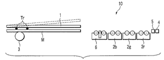
First, a
図1に示すように、パターン形成装置10は、図中矢印T方向に搬送される平板状の凹版1、この凹版1の搬送経路の下方に対向して配置され、凹版1に各色(r:赤、g:緑、b:青)の液体現像剤を供給して現像する複数の現像装置2r、2g、2b(以下、総称して現像装置2と称する場合もある)、および凹版1に保持せしめた現像剤粒子を図中左側に待機している平板状の被転写媒体Mに転写する転写ローラ3(転写装置)を有する。
As shown in FIG. 1, the
また、このパターン形成装置10は、凹版1の後述する高抵抗層13の表面13aを除電する交流コロナ帯電器4、高抵抗層13の表面13aを例えば+400[V]に帯電させる直流コロナ帯電器5(帯電装置)、および転写後の凹版1を次の転写のためにクリーニングするクリーナ6を有する。
The
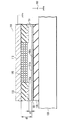
図2Aに平面図を示すように、本実施の形態の凹版1は、矩形平板状に形成されている。この凹版1は、図2Bに断面図を示すように、矩形のガラス板11の表面に例えばアルミニウムなどの導電性の金属層12(基体)を蒸着により形成し、その表面に高抵抗層13を形成して構成されている。高抵抗層13は、例えば、ポリイミド、アクリル、ポリエステル、ウレタン、エポキシ、テフロン(登録商標)、ナイロンなどの体積抵抗率が1010[Ωcm]以上の材料(絶縁体を含む)により形成され、その膜厚は、10[μm]〜40[μm]、好ましくは20[μm]±5[μm]に形成されている。As shown in a plan view in FIG. 2A, the
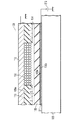
また、この高抵抗層13の表面13aには、図3に部分的に拡大して示すような矩形の凹部14aを多数整列配置したパターン14が形成されている。本実施の形態では、例えば平面型画像表示装置の前面基板に形成する蛍光体スクリーンを製造する版として、1色分の画素に相当する凹部14aだけを高抵抗層13の表面13aから凹ませて形成し、図中破線で示す他の2色分の領域14bには凹部を形成しないでスペースだけを確保してある。図4には、1つの凹部14aを拡大した断面図を示してある。凹部14aの底は、金属層12の表面12aに露出しており、その深さは高抵抗層13の層厚に概ね相当する。
In addition, a
図5には、現像装置2の概略構造を拡大して示してある。上述した各色の現像装置2r、2g、2bは、使用する液体現像剤が異なる以外、同じ構造を有するため、ここでは、現像装置2として説明する。
FIG. 5 shows an enlarged schematic structure of the developing
現像装置2は、凹版1の搬送方向Tに沿って並んだ2つの筐体21、22を有する。凹版1は、そのパターン14が下方に配置された現像装置2に対向する姿勢で搬送される。上流側の筐体21内には、現像ローラ23(供給部材)が設けられている。現像ローラ23は、搬送される凹版1の高抵抗層13の表面13aに対して150±50[μm]程度のギャップを介してその周面が対向する位置に配置され、凹版1の搬送方向と同じ方向(図中時計回り方向)に1.2倍ないし4倍、より好ましくは1.5倍ないし2.5倍の速度で回転する。
The developing
現像ローラ23の凹版1から離間した下方には、現像ローラ23と逆方向に回転するスポンジローラ24が接触配置されている。このスポンジローラ24は、凹版1との対向位置を通過した現像ローラ23の周面に付着している液体現像剤をクリーニングする。また、筐体21の内側面には、現像ローラ23の周面に液体現像剤を供給するためのノズル25が設けられている。
A
液体現像剤は、図示しない現像剤タンクに収容されており、図示しないポンプ等によりノズル25を介して筐体21内に供給される。スポンジローラ24によって回収された余剰の液体現像剤は、筐体21の下端底部に設けられた排出口26を介して現像剤タンクへ回収される。液体現像剤は、絶縁性液体中に帯電した各色の蛍光体粒子(現像剤粒子)を分散させて構成されている。各色の蛍光体粒子は、正に帯電するように金属石鹸などが添加されている。
The liquid developer is accommodated in a developer tank (not shown), and is supplied into the
凹版1の搬送方向に沿って下流側の筐体22内には、スクイズローラ27(除去装置)が設けられている。スクイズローラ27は、その周面が現像ローラ23より凹版1に近接して対向する位置、すなわち、本実施の形態では、高抵抗層13の表面13aから25ないし75[μm]、より好ましくは30ないし50[μm]離間した距離に配置され、凹版1の搬送方向Tと逆方向に回転する。スクイズローラ27は、現像ローラ23によって凹版1に供給された液体現像剤を部分的に除去し、凹版1に残留する液体現像剤の膜厚が1〜30[μm]程度になるようにコントロールする。
A squeeze roller 27 (removal device) is provided in the
スクイズローラ27の周面には、ゴム片により形成されたクリーニングブレード28が接触配置されている。クリーニングブレード28によってスクイズローラ27の周面から回収された余剰の液体現像剤は、筐体22の底部に設けられた排出口29を介して図示しない現像剤タンクへ回収される。
A
図6には、上述したパターン形成装置10の動作を制御する制御系のブロック図を示してある。パターン形成装置10の制御部30には、凹版1を図1(または図5)の矢印T方向に搬送する搬送装置31が接続されている。この搬送装置31は、後述するように、凹版1を逆方向にも搬送する。また、制御部30には、各色の現像装置2r、2g、2bを、それぞれ図5に示す動作位置と凹版1の搬送経路から下方に離間した待機位置との間で移動させる移動機構32が接続されている。また、制御部30には、被転写媒体Mとしてのガラス板Mの図中上方に搬送された凹版1をガラス板Mに対して離接させる離接装置33が接続されている。この離接装置33は、後述するように、凹版1をガラス板Mに傾斜させた状態で近接させ、且つ凹版1をガラス板Mに対して傾斜させた状態で離間させる。さらに、制御部30には、上述した離接装置33によってガラス板Mに対向配置された凹版1をガラス板Mに対して位置決めする位置決め機構34が接続されている。
FIG. 6 is a block diagram of a control system that controls the operation of the
また、制御部30には、各色の現像装置2の現像ローラ23に給電する電源装置35、各色の現像装置2のスクイズローラ27に給電する電源装置36、転写ローラ3に給電する電源装置37、交流コロナ帯電器4に給電する電源装置38、および直流コロナ帯電器5に給電する電源装置39が接続されている。さらに、制御部30には、後述するように各色の蛍光体層をガラス板Mに転写した後、次の色の蛍光体層の転写のために、ガラス板Mに不所望に残留した電荷を除去する電荷除去装置40が接続されている。
Further, the
次に、上述したパターン形成装置10の動作について、図1とともに図7乃至図13を参照して説明する。なお、ここでは、平面型画像表示装置の前面基板の内面に各色の蛍光体層を形成する場合を例にとって説明する。
Next, the operation of the
まず、制御部30は、搬送装置31を制御して、図1に示すように、凹版1を図示矢印T方向に一定速度で搬送する。このとき、交流コロナ帯電器4が、図示しないコロナワイヤーに交流の高電圧を印加し、凹版1の高抵抗層13の表面13aを除電する。また、その直後に、直流コロナ帯電器5は、コロナワイヤーに正極性の高電圧を印加し、正コロナを発生し、凹版1の高抵抗層13の表面13aを例えば+400[V]に帯電する。
First, the
また、制御部30は、上記のように凹版1を搬送して高抵抗層13の表面13aを帯電させるとともに、移動機構32を制御して1色目の赤色現像を実行する現像装置2rを動作位置(図5に図示した位置)へ配置する。そして、制御部30は、現像装置2rを介して赤色の蛍光体粒子を含む液体現像剤を凹版1の高抵抗層13の表面13aへ供給する。このとき、液体現像剤は、図5で反時計回り方向に回転する現像ローラ23の周面によって厚さ数百[μm]程度の液膜として搬送され、この液膜が凹版1の高抵抗層13の表面13aに接触して供給される。なお、この際、高抵抗層13の表面13aに形成されたパターン14の凹部14a内にも液体現像剤が供給される。
Further, the
また、このとき、制御部30は、図13に示すように、電源装置35を介して現像ローラ23に+200[V]の電圧を印加して、例えば接地されている凹版1の金属層12と現像ローラ23との間に第1の電位差を形成する。すると、現像ローラ23と凹版1との間に接触して介在された液体現像剤中の正帯電された蛍光体粒子は、この第1の電界によって、+400[V]に帯電された高抵抗層13の表面13aから反発されるとともに、接地電位の金属層12が凹部14aの底に露出した表面12aに電位差200[V]の作用によって引き付けられ、両者の作用によって蛍光体粒子が凹部14a内に凝集される。これにより、パターン14の各凹部14a内に所望する厚さ(例えば15[μm])の蛍光体層が形成される。
At this time, as shown in FIG. 13, the
このように、赤色現像剤による現像が終了すると、現像ローラ23の周面がスポンジローラ24によってクリーニングされて、凹版1に供給されなかった液体現像剤が排出口26を介して図示しないタンクへ回収される。
As described above, when the development with the red developer is completed, the peripheral surface of the developing
上述した赤色現像剤の現像の直後には、凹版1の高抵抗層13の表面13aに厚さ100[μm]程度の液膜が付着しており、その内部にはパターン14の凹部14a内に凝集されなかった蛍光体粒子が浮遊している。すなわち、この液膜は、理想的には、その殆どを絶縁性液体が占めていることになる。つまり、凹版1のパターン14以外に蛍光体粒子が浮遊しているとカブリの原因になるため、スクイズローラ27によってこの液膜を絞ると同時に、浮遊している蛍光体粒子をスクイズローラ27の表面に付着させて回収する必要がある。
Immediately after the development of the red developer described above, a liquid film having a thickness of about 100 [μm] adheres to the
このとき、スクイズローラ27には、電源装置36を介して200[V]±50[V]程度の電圧が印加され、この電圧により、液膜内に浮遊している蛍光体粒子がスクイズローラ27に引き付けられる。スクイズローラ27による絞り工程を通過した凹版1の高抵抗層13の表面13aには、この時点で、厚さ1〜30[μm]程度の液膜が残留している。言い換えると、この程度の液膜が凹版1の表面に残留するようにスクイズローラ27による液膜の除去量がコントロールされる。すなわち、1色目の現像が終了した凹版1は、濡れた状態を維持したまま次の転写工程へ搬送される。
At this time, a voltage of about 200 [V] ± 50 [V] is applied to the
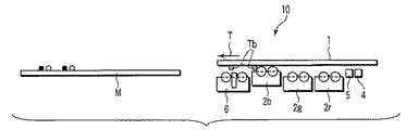
このようにして搬送装置31によって転写工程へ搬送された凹版1は、図1の左側に待機しているガラス板Mの上方に離間して対向配置される。この状態で、凹版1の高抵抗層13の表面13aを濡らした液体現像剤にガラス板Mが接触しない程度に凹版1がガラス板Mから上方に離間している。なお、この状態で、位置決め機構34によって、凹版1がガラス板Mに対して大まかに位置合わせされても良い。
The
この後、離接装置33が動作されて凹版1が図7に破線で示す姿勢に傾斜され、傾斜方向下端となる凹版1の図中左端がガラス板Mに近付けられる。このとき、凹版1に付着した液体現像剤のうち凹版1の図中左端に付着した液体現像剤が先にガラス板Mに接触する。そして、離接装置33によって、傾斜した凹版1が図中実線で示すガラス板Mと平行な姿勢になるまでガラス板Mに徐々に近付けられる。これにより、凹版1を濡らした液体現像剤は、ガラス板Mに対する接触領域が図中右側に徐々に広くなり、最終的にはガラス板Mと凹版1が液膜を介して全面で接触する。このときの凹版1の姿勢を図7に実線で示してある。
Thereafter, the separating / connecting
以上のように、液体現像剤を保持した凹版1をガラス板Mに近付ける際に、両者の間に介在される液体現像剤の液膜がガラス板Mに徐々に接触するように近接させることにより、液膜に過度の乱流が生じることを防止できる。これにより、液膜に過度の乱流が生じてパターン14の凹部14a内に凝集された蛍光体粒子が流出してしまうような不具合を抑制することができる。同様の理由により、後述するように凹版1をガラス板Mから離間させる場合にも、凹版1を傾斜させてガラス板Mに対して徐々に引き剥がすことが望ましい。
As described above, when the
この後、上述したように液膜を介して凹版1とガラス板Mを接触させた状態で、位置決め機構34によって凹版1とガラス板Mを位置合わせする。このとき、位置決め機構34は、凹版1とガラス板Mの双方に予め刻印した位置合わせマークを光学的な手段を用いて読み取って、両者間のズレを検出して、このズレを補正するように凹版1とガラス板Mを相対的に移動させる。移動の際には、両者の間に介在された液体現像剤に乱流を生じることのないように、ゆっくりとした速度で移動させることが望ましい。
Thereafter, the
以上のように、凹版1とガラス板Mを高精度に位置合わせした後、ガラス板Mの凹版1から離間した背面(図中下面)に接触配置した転写ローラ3を介して、負の高電圧を印加する。より具体的には、図14に示すように、ガラス板Mの背面に押圧配置された導電性弾性ローラ3に、電源装置37を介して、例えば、−7[KV]程度の負の高電圧を印加して、ガラス板Mと凹版1の金属層12との間に第2の電位差を形成し、凹部14a内に凝集された正帯電の蛍光体粒子をクーロン力でガラス板Mの表面に転写する。これにより、パターン14と同じ形の赤色の蛍光体層Trがガラス板Mの表面に転写される。
As described above, after aligning the
本実施の形態の装置では、従来のコロナ転写器を用いる場合に比べ、転写ローラ3を介してより強力な転写電界を形成でき、転写特性を大幅に向上させることができる。また、転写時の電界が凹版1からガラス板Mに向かう方向に形成されるため、パターン14の凹部14a内に凝集されていた蛍光体粒子が真っ直ぐガラス板Mに向かって泳動し、パターン14がそのままの形状を保ってガラス板Mに転写される。
In the apparatus of the present embodiment, a stronger transfer electric field can be formed via the
このように、蛍光体粒子がガラス板Mに転写された後、上述したように離接装置33が動作されて、凹版1が徐々に傾斜されてガラス板Mから徐々に離間され、凹版1がガラス板Mの上方に剥離される。つまり、凹版1とガラス板Mとの間に濡れた液膜に過度の乱流を生じないように両者を剥離することで、ガラス板Mに転写された不安定な(定着されていない)蛍光体粒子がガラス板Mから離れしまう不具合を抑制でき、転写済の蛍光体層Trを保護できる。
As described above, after the phosphor particles are transferred to the glass plate M, the separation /
この様にしてガラス板Mから剥離された凹版1は、図8に示すように搬送装置31によって図中右方に搬送される。このとき、クリーナ6が図示しない昇降機構によって図示の動作位置へ上昇され、凹版1の高抵抗層13の表面13aに残留した液体現像剤がクリーニングされる。
The
なお、この後、次の色の蛍光体粒子の転写に備え、転写済の赤色の蛍光体層Trに含まれる樹脂成分を溶融させてガラス板Mにある程度定着させても良い。これにより、次の色の蛍光体粒子を転写した際に2色の蛍光体粒子が混ざってしまう不具合を防止できる。しかし、前の色の蛍光体層をガラス板Mに定着させなくとも、次の色の転写時においても転写ローラ3を介して比較的強い転写電界を付与できるため、ガラス板Mに転写された蛍光体粒子が剥離する方向の電界が作用することはなく、上述したような混色の問題もほとんど心配はない。
Thereafter, the resin component contained in the transferred red phosphor layer Tr may be melted and fixed to the glass plate M to some extent in preparation for the transfer of the phosphor particles of the next color. Thereby, when transferring the phosphor particles of the next color, it is possible to prevent a problem that the phosphor particles of two colors are mixed. However, a relatively strong transfer electric field can be applied through the
また、赤色の蛍光体層の転写が終了した後、電荷除去装置40を動作させてガラス板Mに残留した不所望な電荷を除去する。この際、コロナ帯電やエックス線などによってガラス板Mの表面に残留した電荷を除去する方法や、ガラス板Mを100[℃]〜200[℃]程度の高温で3分から30分程度加熱してガラス板Mの内部に残留した電荷を除去する方法などがある。これにより、次の色の蛍光体層をガラス板Mに転写する際に、残留した電荷が転写電界を打ち消す方向に作用することを防止でき、2色目以降の転写特性を劣化させる不具合を防止できる。以上の処理動作によって、赤色の現像動作が終了する。
In addition, after the transfer of the red phosphor layer is completed, the
この後、上述した赤色現像と同様に、クリーニングされてイニシャライズされた凹版1が再び図中左方に搬送されて、凹版1の表面13aが+400[V]の正電荷に帯電され、図9に示すように、緑色の現像装置2gが動作位置へ上昇されて緑色の蛍光体粒子を含む液体現像剤によってパターン14が現像される。このとき、現像ローラ23と金属層12との間に付与される電位差は、上述した赤色現像のときの電位差と必ずしも同じに設定するものとは限らず、各色の現像剤の特性に合わせて適宜設定される。
Thereafter, in the same manner as in the red development described above, the cleaned and initialized
そして、このように緑色の蛍光体粒子による現像がなされた凹版1は、図中左方に待機しているガラス板Mの上方に再び搬送されて、液体現像剤を介してガラス板Mに接触した後、緑色の蛍光体層Tgが赤色の蛍光体層Trに並んでガラス板Mの表面に転写される。
Then, the
このとき、凹版1は、位置決め機構34によって、図10に示すように、1画素分だけ位置をずらしてガラス板Mに対して位置決め配置され、ガラス板Mの表面上で、緑色の蛍光体粒子Tgが赤色の蛍光体粒子Trのパターンの隣に高精度に位置合わせした状態で転写される。
At this time, as shown in FIG. 10, the
同様にして、青色の蛍光体層Tbが緑色の蛍光体層Tgの隣の所定の位置に転写され(図11、12)、フラットパネルディスプレイ用前面パネルの3色蛍光体パターンの転写が完了する。この後、3色の蛍光体層Tr、Tg、Tbを例えば100[℃]程度の高温に加熱してその樹脂成分を溶融し、ガラス板Mの表面に定着しても良いし、300ないし600[℃]程度の温度で加熱して樹脂成分を蒸発させても良い。 Similarly, the blue phosphor layer Tb is transferred to a predetermined position next to the green phosphor layer Tg (FIGS. 11 and 12), and the transfer of the three-color phosphor pattern on the front panel for a flat panel display is completed. . Thereafter, the phosphor layers Tr, Tg, and Tb of the three colors may be heated to a high temperature of, for example, about 100 [° C.] to melt their resin components and fixed on the surface of the glass plate M, or 300 to 600 The resin component may be evaporated by heating at a temperature of about [° C.].
以上のように、本実施の形態によると、各色の蛍光体粒子の転写時において、液膜を介して凹版1とガラス板Mを対向配置した状態で、位置決め機構34によって両者を高精度に位置合わせするようにしたため、各色の蛍光体パターンの位置合せ精度が極めて高く、例えば±5[μm]程度の位置精度をキープできる。また、各色の蛍光体層Tr、Tg、Tbは、深さ20[μm]前後の凹部14a内から転写されるため、従来のように平坦なプレートから転写する場合に比べ、著しく形状の乱れが少ない厚膜の高品位のパターンを形成できる。
As described above, according to the present embodiment, at the time of transferring the phosphor particles of each color, the
また、本実施の形態によると、1色の蛍光体層のガラス板Mへの転写が終了した後、ガラス板Mに不所望に残留した電荷を電荷除去装置40によって除去するようにしたため、次の色の蛍光体層を転写する際の転写特性が劣化することを防止でき、各色の蛍光体層Tr、Tg、Tbを略同じ転写条件で安定してガラス板Mへ転写することができる。
In addition, according to the present embodiment, after the transfer of the phosphor layer of one color to the glass plate M is completed, the charge remaining undesirably on the glass plate M is removed by the
なお、上述した実施の形態では、3色の蛍光体層Tr、Tg、Tbをガラス板Mの表面上に規則的に並べてパターニングする場合について説明したが、例えば、本実施の形態のパターン形成装置10を用いて3色のカラーフィルタ層をガラス板Mの表面上に形成し、その上に各色の蛍光体層Tr、Tg、Tbを重ねて転写することもできる。
In the above-described embodiment, the case where the three color phosphor layers Tr, Tg, and Tb are regularly arranged and patterned on the surface of the glass plate M has been described. For example, the pattern forming apparatus according to the
また、上述した実施の形態では、平板状の凹版1と平板状のガラス板Mを用いてパターンを形成する場合について説明したが、これに限らず、凹版1またはガラス板M(被転写媒体)の少なくとも一方を円筒形状にすることもできる。この場合、上述した第1の実施の形態のように離接装置33によって凹版1を傾斜させつつガラス板Mに対して離接させる必要はなく、両者の間に介在される液膜に過度の乱流を生じる心配がない。
In the embodiment described above, the case where the pattern is formed using the
次に、この発明の第2の実施の形態に係るパターン形成装置50について図15を参照して説明する。なお、以下の説明では、上述した第1の実施の形態と同様に機能する構成要素には同一符号を付してその詳細な説明を省略する。
Next, a
図15に示すように、パターン形成装置50は、円筒形のドラム状に形成された凹版51を有する。この凹版51は、ここでは図示しないが、例えば、厚さ3[mm]のアルミニウムの円筒(金属層12に相当)の周面に厚さ20[μm]の高抵抗層13を設け、この高抵抗層13に例えばレーザーアブレーションによって凹部14aを設けて形成されている。
As shown in FIG. 15, the
この凹版51を用いてガラス板Mに3色の蛍光体パターンを形成する場合、まず、交流コロナ帯電器4によって凹版51の周面を除電し、直流コロナ帯電器5によって凹版51の高抵抗層13の表面13aを正に帯電する。そして、現像装置2rで赤色の蛍光体粒子を凹版51の凹部14aに凝集させて赤色のパターン14を現像する。
When a three-color phosphor pattern is formed on the glass plate M using the
一方、ガラス板Mは、搬送装置31によって図中右方から左方に向かって一定速度で搬送され、転写ローラ3と凹版51の間に進入する。転写ローラ3は、例えばゴム硬度40度の導電性ゴムローラにより形成され、電源装置37を介して−7[KV]の電圧が印加されている。また、転写ローラ3と凹版51の間に進入されるガラス板Mには、例えば転写ローラ3の長手方向あたり1[Kg/cm]の加重が加えられる。この条件下で、ガラス板Mに赤色の蛍光体層Trが転写される。転写にあたっては、ガラス板Mと凹版51に刻印された位置合わせマークを位置決め機構34で検知し、両者の相対移動を高精度に制御しつつ転写を行う。
On the other hand, the glass plate M is conveyed at a constant speed from the right to the left in the drawing by the conveying
この後、凹版51の高抵抗層13の表面13aは、クリーナ6でクリーニングされ、次の色の蛍光体層の現像および転写のため除電および帯電がなされる。また、ガラス板Mは、搬送装置31によって逆方向に搬送されて初期位置へ戻され、電荷除去装置40によって不所望な残留電荷が除去される。
Thereafter, the
さらにこの後、上述した現像および転写工程を繰り返し、ガラス板M上に3色の蛍光体層Tr、Tg、Tbを転写する。そして、最後に、転写した3色の蛍光体層を溶融してガラス板Mに定着する。 Thereafter, the development and transfer steps described above are repeated to transfer the three color phosphor layers Tr, Tg, and Tb onto the glass plate M. Finally, the transferred three-color phosphor layers are melted and fixed on the glass plate M.
以上のように、本実施の形態によると、凹版51を円筒形にしたため、装置構成を小型化でき、省スペース化を図ることができる。また、本実施の形態では、凹版51を円筒形に形成したことで、平板状のガラス板Mに対して凹版51を徐々に離接させることができ、両者の間に介在する液膜に乱流を生じることを抑制でき、ガラス板Mに転写した蛍光体層が剥離してしまう不具合を防止できる。
As described above, according to the present embodiment, since the
また、本実施の形態のパターン形成装置50を用いて、ガラス板M上にブラックマトリックスをまず転写し、引き続いてカラーフィルタを転写し、最後に蛍光体層を転写することも、装置構成をアレンジすることで可能になる。
In addition, using the
なお、上述した第1および第2の実施の形態では、1色分の凹部14aによるパターン14を有する凹版1、51を用いて、ガラス板Mの表面に各色の蛍光体層Tr、Tg、Tbを3回転写する場合について説明したが、これに限らず、3色分の凹部14aを有する単一の凹版を用いて3色の蛍光体層Tr、Tg、Tbをガラス板Mに一括して転写するようにしても良い。この場合、例えば、図3で説明した1色分の凹部14aの他に破線で示したスペース14bにも凹部14aを形成し、各色用の凹部14aをそれぞれ独立して接続する図16および図17に示すような電極を金属層12の代りに設ければ良い。
In the first and second embodiments described above, each color phosphor layer Tr, Tg, Tb is formed on the surface of the glass plate M by using the
例えば、上述した第2の実施の形態の円筒形の凹版51を改良する場合、図16に示すように、アルミニウムのドラム素管52の表面に例えば厚さ30[μm]の絶縁層53を形成し、その上に画素電極としての銅電極54と保護層としてのニッケル電極55(以下、総称して画素電極56と称する)を設け、さらにその上に高抵抗層13を設けて、最後に、画素電極56に対向する位置の高抵抗層13をエッチング等で除去して凹部14aを形成する。
For example, when the
図17に示すように、各色の画素電極56は、同じ色の画素電極56同士が接続されて異なる色の画素電極56と電気的に分離され、各色毎に異なる電圧を印加できるようになっている。例えば2つの赤色の画素電極56rは、電源ライン57rと58rを介して、不図示の赤用電源に接続されている。同様にして緑色の画素電極56gは、電源ライン57gと58gを介して図示しない緑用電源に接続され、青色の画素電極56bは、電源ライン57b、58bを介して図示しない青用電源に接続されている。
As shown in FIG. 17, the
このように各色の画素電極56を独立して配線することで、単一の凹版を用いて3色の蛍光体パターンを現像できる。例えば、赤色の蛍光体パターンを現像する場合、赤色の画素電極56rのみを接地電位にして、緑色と青色の画素電極56g、56bを+400[V]とすることにより、正帯電した赤色の蛍光体粒子が赤色の画素電極56rにのみ引き付けられて現像される。同様にして、緑色の蛍光体パターンを現像する場合、緑色の画素電極56gのみを接地電位にして、赤色と青色の画素電極56r、56bを+400[v]とすることにより、緑色の蛍光体粒子が緑色の画素電極56gにのみ引き付けられて現像される。さらに、青色の蛍光体パターンを現像する場合、青色の画素電極56bのみを接地電位にして、赤色と緑色の画素電極56r、56gを+400[v]とすることにより、青色の蛍光体粒子が青色の画素電極56bにのみ引き付けられて現像される。このようにして、3色の蛍光体パターンが単一の凹版に現像される。
Thus, by independently wiring the
この後、3色の蛍光体パターンは、ガラス板Mに一括転写される。つまり、3色の蛍光体パターンを同時に保持可能な凹版を使用することで、ガラス板Mへの転写を一括して実施でき、ガラス板Mの内部電荷による2回目以降の転写不良を回避でき、且つ高精度の位置あわせも1回のみで良くなる。 Thereafter, the three-color phosphor patterns are collectively transferred to the glass plate M. In other words, by using an intaglio that can simultaneously hold the three-color phosphor patterns, transfer to the glass plate M can be performed in a lump, and second and subsequent transfer failures due to internal charges of the glass plate M can be avoided, In addition, high-precision positioning only needs to be performed once.
次に、この発明の第3の実施の形態に係るパターン形成装置60について図18を参照して説明する。このパターン形成装置60は、凹版1とガラス板Mとの間に中間転写体61を配置した以外、上述した第1の実施の形態のパターン形成装置10と同じ構造を有する。なお、以下に説明する各実施の形態における中間転写体は、本発明の被転写媒体として機能する場合もある。
Next, a pattern forming apparatus 60 according to a third embodiment of the present invention will be described with reference to FIG. The pattern forming apparatus 60 has the same structure as the
このパターン形成装置60を用いてガラス板Mの表面に3色の蛍光体層Tr、Tg、Tbを形成する場合、一旦、中間転写体61の周面上に各色の蛍光体層Tr、Tg、Tbを転写した後、これら3色の蛍光体層Tr、Tg、Tbを一括してガラス板Mに転写する。
When the three color phosphor layers Tr, Tg, and Tb are formed on the surface of the glass plate M using the pattern forming device 60, the phosphor layers Tr, Tg, and Tb of the respective colors are temporarily formed on the peripheral surface of the
すなわち、凹版1に対して現像装置2rを介して赤色の蛍光体粒子を現像し、凹版1の凹部14aに凝集されている赤色の蛍光体パターンを導電性を有する中間転写体61の周面に電界の作用で転写する。この際、例えば上述した第1の実施の形態のようにガラス板Mの背面側から高電圧を印加する場合と異なり、中間転写体61は表面もしくは表面近傍に導電性電極が存在するため、−200[V]程度の転写電圧でも極めて良好な形状の蛍光体層を高効率で転写することができる。
That is, red phosphor particles are developed on the
同様にして、緑色の蛍光体パターンおよび青色の蛍光体パターンを中間転写体61の周面上に並べて転写する。このように、繰り返し3色の蛍光体パターンを中間転写体61に転写する際にも、例えば上述した第1の実施の形態のガラス板Mのときのように転写特性が劣化することはない。
Similarly, the green phosphor pattern and the blue phosphor pattern are transferred side by side on the peripheral surface of the
また、中間転写体61に2色目以降の蛍光体パターンを転写する際には、前に転写済の蛍光体パターンが潰れる可能性も考えられる。このため、中間転写体61の周面に図示しないスペーサなどを設けてこの周面と凹版1との間に物理的なギャップを確保するようにしても良い。
Further, when transferring the second and subsequent phosphor patterns to the
上記のように中間転写体61の周面に転写された3色の蛍光体層Tr、Tg、Tbは、中間転写体61の回転によって搬送され、ガラス板Mに一括して転写される。なお、このように中間転写体61を用いて3色の蛍光体層Tr、Tg、Tbをガラス板Mに転写する場合、特に、中間転写体61からガラス板Mに蛍光体層を転写するときに蛍光体層が絶縁性液体によって濡れていることが望ましい。
The three-color phosphor layers Tr, Tg, and Tb transferred to the peripheral surface of the
以上のように、本実施の形態によると、中間転写体61上に3色の蛍光体層Tr、Tg、Tbを転写した後、これら3色の蛍光体層Tr、Tg、Tbを一括してガラス板Mに転写するようにしたため、ガラス板Mへの転写を1回で済ませることができる。これにより、上述した第1の実施の形態で説明したようなガラス板M内部に電荷が蓄積する問題も生じない。
As described above, according to the present embodiment, after the three color phosphor layers Tr, Tg, and Tb are transferred onto the
次に、この発明の第4の実施の形態に係るパターン形成装置70について図19を参照して説明する。このパターン形成装置70は、各色用の凹版1r、1g、1bを有し、平板状の中間転写体71を有する点において、上述した実施の形態と異なる。つまり、このパターン形成装置70は、平板状の複数の凹版を用いたいわゆるタンデム方式を採用したものとなっている。
Next, a
このパターン形成装置70を用いて3色の蛍光体層Tr、Tg、Tbをガラス板Mに転写する場合、まず、中間転写体71の搬送経路から外れた位置で、赤色用の凹版1rに現像装置2rを介して赤色の蛍光体粒子が供給されて赤色の蛍光体パターンが現像される。このように、赤色の蛍光体パターンが現像された凹版1rは、中間転写体71の搬送経路上へ移動されて中間転写体71に対向配置され、保持している赤色の蛍光体パターンが中間転写体71へ転写される。
When transferring the three-color phosphor layers Tr, Tg, and Tb to the glass plate M using the
同様にして、緑色の蛍光体パターンが中間転写体71に赤色の蛍光体パターンに並べて転写され、青色の蛍光体パターンが中間転写体71に赤色および緑色の蛍光体パターンに並べて転写される。 Similarly, the green phosphor pattern is transferred to the intermediate transfer body 71 along with the red phosphor pattern, and the blue phosphor pattern is transferred onto the intermediate transfer body 71 along with the red and green phosphor patterns.
そして、中間転写体71の搬送経路の終点に待機しているガラス板Mに3色の蛍光体パターンを保持した中間転写体71が対向配置され、3色の蛍光体層Tr、Tg、Tbが一括してガラス板Mへ転写される。 Then, the intermediate transfer body 71 holding the three-color phosphor patterns is disposed opposite to the glass plate M waiting at the end point of the conveyance path of the intermediate transfer body 71, and the three-color phosphor layers Tr, Tg, Tb are arranged. It is transferred to the glass plate M at once.
以上のように、本実施の形態においても、上述した第3の実施の形態と同様に、ガラス板Mへの転写を1回にすることができ、その上、平板同士の転写なので高い位置合せ精度を実現できる。また、本実施の形態によると、各色の転写ステーションを通して中間転写体71を高速に移動させてガラス板Mへ蛍光体層を転写できるため、他の実施の形態の装置と比較してより高速な処理が可能となる。 As described above, also in this embodiment, as in the third embodiment described above, transfer to the glass plate M can be performed once, and furthermore, since the transfer between the flat plates, high alignment is achieved. Accuracy can be achieved. In addition, according to the present embodiment, the phosphor layer can be transferred to the glass plate M by moving the intermediate transfer body 71 at high speed through each color transfer station, so that it is faster than the apparatus of the other embodiments. Processing is possible.
次に、この発明の第5の実施の形態に係るパターン形成装置80について図20を参照して説明する。このパターン形成装置80は、上述した第2の実施の形態で説明した円筒状の凹版51と、上述した第3の実施の形態で説明した円筒状の中間転写体61と、を組み合わせたことを特徴としている。
Next, a
このパターン形成装置80を用いて3色の蛍光体層Tr、Tg、Tbをガラス板Mに転写する場合、まず、凹版51に現像装置2rを介して赤色の蛍光体粒子を供給して赤色の蛍光体パターンを現像し、この赤色の蛍光体パターンを中間転写体61に転写する。同様にして、緑色の蛍光体パターン、および青色の蛍光体パターンを順次中間転写体61に転写し、最後に3色の蛍光体パターンを一括して中間転写体61からガラス板Mへ転写する。
When transferring the three color phosphor layers Tr, Tg, and Tb to the glass plate M using the
以上のように、本実施の形態によると、凹版51および中間転写体61をそれぞれ円筒形としたため、装置構成を小型化でき、省スペース化を図ることができる。また、円筒形の凹版51から円筒形の中間転写体61へ蛍光体パターンを転写する際には、両者の間に介在される液体現像剤の乱流が殆ど生じることがなく、蛍光体粒子が飛散してしまうこともない。また、中間転写体61からガラス板Mへ蛍光体パターンを転写する際にも同様の効果を奏することができる。
As described above, according to the present embodiment, since the
また、本実施の形態のように円筒形の中間転写体61に平板状のガラス板Mを殆ど接触させた状態で対向させる場合には、ガラス板Mのたわみを利用して中間転写体61の周面とガラス板Mとの間のギャップを適切な値に保持できる。
Further, when the flat glass plate M is opposed to the cylindrical
図21には、この発明の第6の実施の形態に係るパターン形成装置100の概略斜視図を示してある。
このパターン形成装置100は、図中時計回り方向(矢印R方向)に回転するドラム素管(後述する)の周面に巻かれた原版101(像保持体)、この原版101の後述する高抵抗層に電荷を与えて帯電させる帯電器102、原版101に各色(r:赤、g:緑、b:青)の液体現像剤を供給して現像する複数の現像装置103r、103g、103b(以下、総称して現像装置103と称する場合もある)、現像によって原版101に付着した液体現像剤の溶媒成分をエアブローによって気化して乾燥させる乾燥器104(乾燥装置)、原版101に付着した現像剤粒子を転写してパターンを形成する被転写媒体となるガラス板105を定位置で保持するステージ106(保持機構)、転写に先立ってガラス板105の表面に高抵抗もしくは絶縁性の溶媒を塗布する塗布装置107(濡らし装置)、転写を終えた原版101をクリーニングするクリーナ108、および原版101の電荷を除去する除電器109を有する。FIG. 21 is a schematic perspective view of a
The
各色の現像装置103r、103g、103bに収納される液体現像剤は、炭化水素系やシリコーン系などの絶縁性溶媒中に帯電した微粒子(現像剤粒子)を分散したもので、この微粒子が電界で電気泳動することによって現像が行われる。微粒子としては、例えば平均粒径4[μm]程度の各色の蛍光体粒子をこれよりも平均粒径が小さい樹脂粒子が取り囲み、樹脂粒子がイオン性帯電サイトを有していて電界中でイオン解離することで電荷を帯びる構成や、樹脂粒子の内部に各色の顔料微粒子を内包する構成、もしくは樹脂粒子の表面に各色の顔料微粒子を担持する構成などが実施可能である。
The liquid developer accommodated in each
図22Aに平面図を示すように、原版101は、矩形の薄板状に形成されている。この原版101は、図22Bに断面図を示すように、厚さ0.05[mm]ないし0.4[mm]、より好ましくは厚さ0.1[mm]ないし0.2[mm]の矩形の金属フィルム112の表面に高抵抗層113を形成して構成されている。金属フィルム112は可撓性を有し、アルミニウム、ステンレス、チタン、アンバーなどの素材で構成可能であるほかに、ポリイミドやPETなどの表面に金属を蒸着したものなどでも良いが、転写パターンを高い位置精度で形成するためには、熱膨張や応力による伸びなどが生じにくい素材で構成することが望ましい。また、高抵抗層113は、例えば、ポリイミド、アクリル、ポリエステル、ウレタン、エポキシ、テフロン(登録商標)、ナイロンなどの体積抵抗率が1010[Ωcm]以上の材料(絶縁体を含む)により形成され、その膜厚は、10[μm]〜40[μm]、より好ましくは20[μm]±5[μm]に形成されている。As shown in the plan view of FIG. 22A, the
また、原版101の高抵抗層113の表面113aには、図23に部分的に拡大して示すような矩形の凹部114aを多数整列配置したパターン114が形成されている。本実施の形態では、例えば平面型画像表示装置の前面基板に形成する蛍光体スクリーンを製造する凹版として、1色分の画素に相当する凹部114aだけを高抵抗層113の表面113aから凹ませて形成し、図23中に破線で示す他の2色分の領域114bには凹部を形成しないでスペースだけを確保してある。
Further, a
図24には、1つの凹部114aを拡大した原版101の断面図を示してある。本実施の形態では、凹部114aの底には金属フィルム112の表面112aが露出しており、この金属フィルム112の露出した表面112aがこの発明のパターン状の電極層として機能する。凹部114aの深さは、高抵抗層113の層厚に概ね相当する。凹部114aの底に露出した金属フィルム112の表面112a、および高抵抗層113の表面113aを含む原版101の表面全体に、厚さ0.5[μm]ないし3[μm]程度の表面離型層をコーティングすれば、転写特性が向上しより好ましい特性が得られる。
FIG. 24 shows a cross-sectional view of the original 101 in which one
図25には、上記構造のフィルム状の原版101をドラム素管131に巻きつける様子を描いた概略断面図を示してある。ドラム素管131の図中上部の切り込み部131aには、原版101の一端を固定するクランプ132と他端を固定するクランプ133が設けられている。原版101をドラム素管131の周面上に巻き付ける場合、まず、原版101の一端をクランプ132に固定し、その後、原版101を架張しつつその他端134をクランプ133で固定する。これにより、たるみ無く原版101をドラム素管131周面の規定位置に巻き付けることができる。
FIG. 25 is a schematic cross-sectional view illustrating a state where the film-shaped
図26は、このようにしてドラム素管131に巻きつけられた原版101の高抵抗層113の表面113aを帯電器104によって帯電する工程を説明するための部分構成図である。帯電器104は、周知のコロナ帯電器であり、コロナワイヤー142とシールドケース143で基本的に構成されているが、メッシュ状のグリッド144を設けることで帯電の均一性を向上できる。例えば、原版101の金属フィルム112とシールドケース143を接地し、コロナワイヤー142に不図示の電源装置によって+5.5[kV]の電圧を印加し、更にグリッド144に+500[V]の電圧を印加して原版101を図中矢印R方向に移動させると、高抵抗層113の表面113aは略+500[V]に均一に帯電される。
FIG. 26 is a partial configuration diagram for explaining a process of charging the
同図に示した除電器109は、帯電器104とほぼ同様の構造であるが、コロナワイヤー146に例えば実効電圧6[kV]、周波数50[Hz]の交流電圧を印加すべく不図示の交流電源に接続し、シールドケース147とグリッド148を設置すると、帯電器104による帯電に先立って原版101の高抵抗層113の表面113aを略0[V]となるよう除電することが可能で、高抵抗層113の繰り返し帯電特性を安定化させることができる。
The
図27には、上記のように帯電された原版101に対する現像動作を説明するための図を示してある。現像時には、現像する色の現像器103を原板101に対向させて、その現像ローラ151(供給部材)とスクイズローラ152を原版101に近接させ、原版101に上述した液体現像剤を供給する。現像ローラ151は、搬送される原版101の高抵抗層113の表面113aに対して100〜150[μm]程度のギャップを介してその周面が対向する位置に配置され、原版101の回転方向と同じ方向(図中反時計回り方向)に1.5倍ないし4倍程度の速度で回転する。
FIG. 27 is a diagram for explaining the developing operation for the
不図示の供給系によって現像ローラ151周面に供給される液体現像剤153は、絶縁性液体としての溶媒154に現像剤粒子としての帯電したトナー粒子155を分散させて構成されており、現像ローラ151の回転に伴って原版101の周面に供給される。ここで、現像ローラ151に図示しない電源装置によって例えば+250[V]の電圧を印加すると、正に帯電しているトナー粒子155は、接地電位の金属フィルム112に向かって溶媒154中を泳動し、原版101の凹部114a内に集められる。このとき、高抵抗層113の表面113aは、+500[V]程度に帯電されているので正帯電したトナー粒子155は表面113aから反発されて付着しない。
The
このようにして原版101の凹部114a内にトナー粒子155が集められた後、トナー粒子155の濃度が薄くなった液体現像剤153が引き続いてスクイズローラ152と原版101が対向するギャップに進入する。ここでは、ギャップ(絶縁層113の表面113aとスクイズローラ152表面の間の距離)が30[μm]ないし50[μm]、スクイズローラ152の電位が+250[V]で、スクイズローラ152は原版101とは逆向きに原版101の速度の3倍から5倍程度の速度で移動するように設定されているため、現像をさらに促進しつつ、同時に原版101に付着している溶媒156の一部を絞り取る効果を奏する。このようにして、原版101の凹部114aにトナーによるパターン157が形成される。
After the
ところで、ガラス板105上に3色の蛍光体のパターンを形成する場合、図28に示すように、まず、青色蛍光体粒子を含む液体現像剤を収納する現像器103bが原版101の直下に移動し、ここで図示しない昇降機構によって現像器103bが上昇して原版101に近接させる。この状態で、原板101が矢印R方向に回転して凹部114aによるパターンが現像される。青色パターンの現像が終了すると、現像器103bが下降して原版101から離間する。
By the way, when forming a three-color phosphor pattern on the
この青色現像プロセスの間に、図示しない搬送装置によって予め搬送されてステージ106上に保持されているガラス板105のステージ106から離間した表面に沿って塗布装置107が図中の破線矢印T1方向に移動し、ガラス板105の表面に溶媒(絶縁性液体)が塗布される。この溶媒の役割と材料組成については後述する。
During this blue developing process, the
しかる後に、青色のパターンを周面に担持した原版101が回転しつつ図中の破線矢印T2に沿って移動(この動作を転動と称する)し、青色のパターン像がガラス板105の表面に転写される。転写の詳細についても後述する。青パターンの転写を終えた原版101は図中左方に平行移動し、現像時の初期位置に戻る。このとき、ガラス板105を保持したステージ106が下降して初期位置に戻る原版101との接触が避けられる。
After that, the
次に、3色の現像器103r、103g、103bが図中左方に移動し、緑色の現像器103gが原版101の直下に位置するところで停止し、青色の現像のときと同様にして現像器103gの上昇、現像、下降が行われる。引き続いて上記と同様の操作で緑パターンが原版101からガラス板105の表面に転写される。このとき、緑色のパターンのガラス板105表面上の転写位置は、上述した青色のパターンから1色分ずらされることは言うまでもない。
Next, the three-
そして、上記の動作を赤色の現像についても繰り返し、ガラス板105の表面上に3色パターンを並べて転写して3色のパターン像をガラス板105の表面に形成する。このように、ガラス板105を定位置に保持して固定し、原版101をガラス板105に対して移動させることで、ガラス板105の往復移動が不要になり、大きな移動スペースの確保や装置の大型化を抑制できる。
The above operation is repeated for red development, and three-color patterns are arranged and transferred on the surface of the
図29には、上述した原版101をガラス板105に沿って転動させるための転動機構の要部の構造を示してある。原版101を周面上に巻き付けたドラム素管131の軸方向両端には、ピニオンと呼ばれる歯車171が取り付けられている。原版101は、この歯車171とモーター172の駆動歯車173のかみ合わせによって回転するとともに、ステージ106の両端に設置されている直線軌道のラック174とピニオン(歯車171)の噛み合わせによって図中右方向に並進する。このとき、ステージ106上に保持されたガラス板105の表面と原版101の表面との間に相対的なズレを生じることのないように、転動機構の各部の構造が設計されている。特許請求の範囲では、このように回転しながらガラス板105に沿って平行に移動する動作を転動と称している。
FIG. 29 shows a structure of a main part of a rolling mechanism for rolling the above-described
このようなラック・アンド・ピニオン機構によれば、駆動伝達用のアイドラが無いため、バックラッシュの無い高精度の回転・並進駆動を実現でき、ガラス板105上に例えば±5[μm]といった位置精度の高い高精細パターンを転写することが可能となる。
According to such a rack and pinion mechanism, since there is no drive transmission idler, high-accuracy rotation / translation drive without backlash can be realized, and the position on the
一方、ガラス板105(図29では図示していない)は、図28に示すように、ステージ106の平らな接触面106aに対してその裏面105b(原版101から離間した側の面)の略全面を面接させるようにステージ106上に配置される。その上、ガラス板105には、ステージ106を貫通して接触面106aまで延びた吸気口176に、接続パイプ175から主パイプ177を経由して不図示の真空ポンプを接続することによって、吸気口176の接触面106aに開口した図示しない吸着孔を介して負圧が作用され、ステージ106の接触面106a上に吸着される。この吸着機構によって、ガラス板105は、高い平面度を持った接触面106aにその裏面105bの略全面を押圧させて密着され、平面性が高い状態でステージ106上に保持される。このように平らな接触面106aにガラス板105を押し付けることにより、ガラス板105の歪み等をも矯正でき、後述する原版101との間の転写ギャップを高精度に維持できる。
On the other hand, the glass plate 105 (not shown in FIG. 29) is, as shown in FIG. 28, substantially the
図30は、原版101からガラス板105にトナー粒子155を転写する際の様子を説明する要部断面図である。ガラス板105の表面105aには、例えば導電性高分子などで構成される導電層181が塗布されており、この導電層181の表面181aと原版101の高抵抗層113の表面113aとは、ギャップd2を介して非接触状態に設置される。d2は例えば10[μm]ないし40[μm]の範囲の値に設定される。高抵抗層113の厚さが例えば20[μm]の場合は、金属フィルム112と導電層181表面181aとの間の距離は、30[μm]ないし60[μm]となる。
FIG. 30 is a cross-sectional view of a main part for explaining a state when the
この状態で、電源装置182(転写装置)を介して導電層181に例えば−500[V]の電圧を印加すると、接地電位の金属フィルム112との間に500[V]の電位差が形成され、その電界によってトナー粒子155が溶媒154中を電気泳動して導電層181の表面181aに転写される。このように、トナー粒子155は非接触状態でも転写が可能なので、オフセット印刷やフレキソ印刷の場合のように、ブランケットやフレキソ版といった弾性体を介在させる必要がなく、常に位置精度の高い転写を実現することが可能となる。導電層181は、トナー粒子155の転写後、ガラス板105を図示しないベーク炉へ投入して焼成することで消失させる。
In this state, when a voltage of, for example, −500 [V] is applied to the
なお、上記のように、電界を用いてトナー粒子をガラス板105に転写する場合、転写ギャップに溶媒が存在してガラス板105側の導電層181と原版101との間を濡らすことが必須条件となるため、転写に先立ってガラス板105の表面105aを溶媒でプリウェットしておくことが有効である。プリウェット溶媒としては絶縁性もしくは高抵抗であれば良いが、液体現像剤に用いられている溶媒と同一の溶媒、もしくはこれに帯電制御剤などが添加されたものであればなお好適である。プリウェット溶媒は、図28を用いて説明したように、塗布装置107によって適切なタイミングで適当な塗布量でガラス板105の表面105a上に塗布される。
As described above, when toner particles are transferred to the
以上のように、上述した実施の形態によると、定位置に配置したガラス板105に対して原版101を転動させて現像したトナー粒子155をガラス板105の表面105aに転写するようにしたため、原版101を転動させる転動機構の構成を小型化でき、装置の設置スペースを小さくできる。また、上述した実施の形態によると、非接触状態で対向配置した原版101からガラス板105へ電界を用いてトナー粒子155を転写するようにしたため、従来のようにフレキソ版を用いた転写方式と比較して、転写像の解像度を高めることができ、高精細なパターンを形成できる。
As described above, according to the above-described embodiment, the developed
また、上述した実施の形態では、原版101の凹部114aに集めた(現像した)トナー粒子155を乾燥器104からのエアブローによって一旦適度に乾燥させた後、ガラス板105の表面105aを溶媒によって濡らして(プリウェットして)トナー粒子155を転写するようにしたため、ガラス板105の表面105aに転写されるトナー像の形状を安定させることができ、パターンの輪郭を鮮明にできる。
In the above-described embodiment, the
ここで、上述した第6の実施の形態のいくつかの変形例について図31乃至図33を参照しつつ説明する。なお、ここでは、上述した第6の実施の形態のパターン形成装置100と同様に機能する構成要素については同一符号を付してその詳細な説明を省略するとともに、説明に関係のない構成については図示を省略する。
Here, some modifications of the above-described sixth embodiment will be described with reference to FIGS. 31 to 33. Here, components that function in the same manner as the
図31には、原版101の高抵抗層113の表面113aをガラス板105の表面105a上に設けた導電層181の表面181aに接触させた状態でトナー粒子155を転写する例を示してある。実際のガラス板105は、位置によって厚さのばらつきがあり、ばらつきの大きさが30[μm]に達する場合もあるため、図30のように原版101との間にギャップd2を20[μm]に設定した場合であっても、位置によっては導電層181の表面が図31に示すように高抵抗層113の表面113aに接触することも考えられる。いずれにしても、原版101の凹部114a内に集められたトナー粒子155は、導電層181に対して非接触もしくは軽い接触となるため、電気泳動によって良好な転写が可能となる。
FIG. 31 shows an example in which the
しかしながら、ステージ106の接触面106a上にそのままガラス板105を載置して原版101を導電層181に接触させると、ガラス板105の厚さのばらつき等、両者の間のギャップが変動した場合、その部位で応力が集中して不具合を生じる。このため、原版101とガラス板105を接触させる場合には、図31に示すように、ステージ106の接触面106a上に厚さが高精度に制御された板状の弾性部材191(例えば硬度60度で厚さ1[mm]のウレタンゴムなど)を設け、その上にガラス板105を設置するなどの対策を施すことが有効である。これにより、例えば、ガラス板105に厚さのばらつきがあっても、そのばらつきを弾性部材191が吸収でき、良好な転写特性を維持できる。なお、この場合、原版101とガラス板105との間のギャップを高精度にコントロールする必要がないため、装置構成を簡略化でき安価に製造できる。なお、弾性部材191は必ずしも板状である必要はなく、例えばゴム製の吸盤状の弾性部材をステージ106上に複数設置しこの吸盤でガラス板105を保持する構成であっても良い。この場合には、ゴム製吸盤の応力変形によって、接触状態を制御することができる。
However, when the
図32には、ガラス板105の表面105a上にブラックマトリックスや抵抗層といった構造物201を形成した後、原版101に現像されたトナー粒子155をガラス板105の表面105a上に転写する例を示してある。この例では、高抵抗層113に凹部114aを持たない原版101’を用いた。この場合においても、原版101のトナー粒子155に電界を作用させることで、ガラス板105にトナー粒子155を良好に転写できる。
FIG. 32 shows an example in which the
つまり、この場合、原版101は必ずしも凹版である必要は無く、金属フィルム112の表面と高抵抗層113の表面が同一平面上に存在するいわゆる平版であっても良い。例えば、原版101とガラス板105との間に一定のギャップを設けた場合、高抵抗層113の無い金属フィルム112が露出した表面に集められたトナー粒子155は、導電層181に対して非接触状態となるため良好な電界転写が行われる。また、この場合、ガラス板105上の構造物201がトナー粒子155を区画する隔壁として機能するため、転写するパターンの輪郭をはっきりさせることができる。
That is, in this case, the
図33には、原版101の金属フィルム112とガラス板105との間に転写のための電界を形成するための導電層211(対向電極)を、ガラス板105がステージ106の接触面106aに対面する裏面105b側に設けた例を示してある。この場合であっても、原版101の金属フィルム112とガラス板105の表面105aとの間に十分な電界強度が得られるよう、電源装置212を介して導電層211に印加する電圧を設定すれば、良好な転写を行うことができる。
FIG. 33 shows a conductive layer 211 (counter electrode) for forming an electric field for transfer between the
例えば、ガラス板105の厚さが1.8[mm]の場合には、導電層211には−5[kV]から−7[kV]程度の高電圧を印加すれば十分な電界強度が得られる。この構成であれば、事前にガラス板105の表面105aに導電層181を塗布する必要がなく、ステージ106の接触面106a上に導電層211を予め設置しておくといった簡素な構成が可能となる。また、転写後、不必要な表面側の導電層181を消失させる工程も不要となる。
For example, when the thickness of the
なお、この発明は、上述した実施の形態そのままに限定されるものではなく、実施段階ではその要旨を逸脱しない範囲で構成要素を変形して具体化できる。また、上述した実施の形態に開示されている複数の構成要素の適宜な組み合わせにより種々の発明を形成できる。例えば、上述した実施の形態に示される全構成要素から幾つかの構成要素を削除しても良い。更に、異なる実施の形態に亘る構成要素を適宜組み合わせても良い。 Note that the present invention is not limited to the above-described embodiment as it is, and can be embodied by modifying the constituent elements without departing from the scope of the invention in the implementation stage. Various inventions can be formed by appropriately combining a plurality of constituent elements disclosed in the above-described embodiments. For example, you may delete some components from all the components shown by embodiment mentioned above. Furthermore, you may combine the component covering different embodiment suitably.
例えば、上述した第1乃至第5の実施の形態では、凹版、中間転写体、およびガラス板をいずれか一方のみを他方に対して移動させる場合について説明したが、これに限らず、対向する2つの部材は相対的に移動すれば良い。 For example, in the above-described first to fifth embodiments, the case where only one of the intaglio, the intermediate transfer member, and the glass plate is moved with respect to the other has been described. The two members may move relatively.
また、上述した実施の形態では、蛍光体粒子を正に帯電させてパターン形成装置を動作させる場合について説明したが、これに限らず、全ての構成を逆極性に帯電させて動作させても良い。 In the above-described embodiment, the case where the phosphor particles are positively charged and the pattern forming apparatus is operated has been described. However, the present invention is not limited to this, and all the components may be operated with a reverse polarity. .
また、上述した実施の形態では、平面型画像表示装置の前面基板に蛍光体層やカラーフィルタを形成する装置に本発明を適用した場合についてのみ説明したが、本発明は、他の技術分野における製造装置として広く利用できる。 Further, in the above-described embodiments, only the case where the present invention is applied to an apparatus for forming a phosphor layer or a color filter on a front substrate of a flat-type image display apparatus has been described. However, the present invention is not limited to other technical fields. Can be widely used as manufacturing equipment.
例えば、液体現像剤の組成を変更すれば回路基板やICタグなどにおける導電パターンを形成する装置に本発明を適用することも可能である。この場合には、液体現像剤を、例えば、平均粒径0.3[μm]の樹脂粒子と、その表面に付着している平均粒径0.02[μm]の金属微粒子(例えば銅、パラジウム、銀など)と、金属石鹸のような電荷制御剤から構成すれば、上述した実施の形態と同様の手法により、例えばシリコンウェハー上に現像剤による配線パターンを形成することもできる。一般に、このような現像剤のみで十分な導電性を有する回路パターンを形成することは容易ではないので、パターン形成後に上記の金属微粒子を核としてメッキを施すことが望ましい。このようにして、導電性回路や、コンデンサー、抵抗などのパターニングを行うことも可能である。 For example, if the composition of the liquid developer is changed, the present invention can be applied to an apparatus for forming a conductive pattern on a circuit board or an IC tag. In this case, the liquid developer is, for example, resin particles having an average particle size of 0.3 [μm] and metal fine particles having an average particle size of 0.02 [μm] attached to the surface (for example, copper, palladium, etc.). , Silver, etc.) and a charge control agent such as a metal soap, a wiring pattern made of a developer can be formed on a silicon wafer, for example, by the same method as in the above-described embodiment. In general, it is not easy to form a circuit pattern having sufficient conductivity only with such a developer. Therefore, it is desirable to perform plating using the metal fine particles as a nucleus after pattern formation. In this manner, patterning of a conductive circuit, a capacitor, a resistor, and the like can be performed.
また、上述した実施の形態では、凹部によるパターンが形成されている版を用いた装置について説明したが、これに限らず、例えば、周知の電子写真法によって、感光体表面に静電潜像を形成し、これを液体現像剤で現像して転写する装置にも本発明を適用することができる。 In the above-described embodiment, the apparatus using the plate on which the pattern by the concave portion is formed has been described. However, the present invention is not limited to this. For example, an electrostatic latent image is formed on the surface of the photoreceptor by a known electrophotographic method. The present invention can also be applied to an apparatus for forming, developing this with a liquid developer, and transferring it.
この発明のパターン形成装置は、上記のような構成および作用を有しているので、厚膜のパターンを高い解像度で高精度に形成できる。 Since the pattern forming apparatus of the present invention has the above-described configuration and operation, a thick film pattern can be formed with high resolution and high accuracy.
Claims (38)
絶縁性液体中に帯電した現像剤粒子を分散させた液体現像剤を、上記高抵抗層の表面に対向せしめた供給部材を介して供給するとともに、この供給部材と上記基体との間に第1の電位差を形成し、上記液体現像剤中の上記現像剤粒子を上記凹部内に集めて現像する現像装置と、
上記凹部内に上記現像剤粒子を集められた上記高抵抗層の表面に被転写媒体を近接対向させた状態で、この被転写媒体と上記基体との間に第2の電位差を形成し、上記凹部内に集められた上記現像剤粒子を当該被転写媒体へ転写する転写装置と、
を有することを特徴とするパターン形成装置。An intaglio plate having a high resistance layer on the surface of the conductive substrate and having a pattern formed by a recess recessed from the surface of the high resistance layer toward the substrate;
A liquid developer in which charged developer particles are dispersed in an insulating liquid is supplied through a supply member opposed to the surface of the high resistance layer, and a first member is provided between the supply member and the substrate. A developing device that collects the developer particles in the liquid developer in the recesses and develops them,
A second potential difference is formed between the transfer medium and the substrate in a state where the transfer medium is closely opposed to the surface of the high resistance layer in which the developer particles are collected in the recess. A transfer device for transferring the developer particles collected in the recesses to the transfer medium;
A pattern forming apparatus comprising:
絶縁性液体中に帯電した第1の現像剤粒子を分散させた第1の液体現像剤を、上記高抵抗層の表面に対向せしめた第1の供給部材を介して供給するとともに、この第1の供給部材と上記基体との間に第1の電位差を形成し、上記第1の液体現像剤中の上記第1の現像剤粒子を上記凹部内に集めて現像する第1の現像装置と、
上記凹部内に上記第1の現像剤粒子を集められた状態の上記高抵抗層の表面に被転写媒体を近接対向させた状態で、この被転写媒体と上記基体との間に第2の電位差を形成し、上記凹部内に集められた上記第1の現像剤粒子を当該被転写媒体へ転写する第1の転写装置と、
絶縁性液体中に帯電した第2の現像剤粒子を分散させた第2の液体現像剤を、上記高抵抗層の表面に対向せしめた第2の供給部材を介して供給するとともに、この第2の供給部材と上記基体との間に第3の電位差を形成し、上記第2の液体現像剤中の上記第2の現像剤粒子を上記凹部内に集めて現像する第2の現像装置と、
上記凹部内に上記第2の現像剤粒子を集められた上記高抵抗層の表面に上記第1の現像剤粒子が転写された上記被転写媒体を近接対向させた状態で、この被転写媒体と上記基体との間に第4の電位差を形成し、上記凹部内に集められた上記第2の現像剤粒子を当該被転写媒体へ転写する第2の転写装置と、
を有することを特徴とするパターン形成装置。An intaglio plate having a high resistance layer on the surface of the conductive substrate and having a pattern formed by a recess recessed from the surface of the high resistance layer toward the substrate;
The first liquid developer, in which the first developer particles charged in the insulating liquid are dispersed, is supplied through the first supply member facing the surface of the high resistance layer. A first developing device that forms a first potential difference between the supply member and the substrate, collects the first developer particles in the first liquid developer in the recess, and develops the first developer particles;
A second potential difference between the transfer medium and the substrate with the transfer medium in close proximity to the surface of the high resistance layer in which the first developer particles are collected in the recess. A first transfer device that transfers the first developer particles collected in the recess to the transfer medium;
A second liquid developer in which charged second developer particles are dispersed in an insulating liquid is supplied through a second supply member facing the surface of the high resistance layer, and the second liquid developer is supplied. A second developing device that forms a third potential difference between the supply member and the substrate, collects the second developer particles in the second liquid developer in the recess, and develops the second developer particles;
In a state where the transfer medium on which the first developer particles are transferred is closely opposed to the surface of the high resistance layer in which the second developer particles are collected in the recess, A second transfer device that forms a fourth potential difference with the substrate and transfers the second developer particles collected in the recess to the transfer medium;
A pattern forming apparatus comprising:
絶縁性液体中に帯電した第1の現像剤粒子を分散させた第1の液体現像剤を、上記高抵抗層の表面に対向せしめた第1の供給部材を介して供給するとともに、この第1の供給部材と上記第1の電極との間に第1の電位差を形成し、上記第1の液体現像剤中の上記第1の現像剤粒子を上記第1の凹部内に集めて現像する第1の現像装置と、
絶縁性液体中に帯電した第2の現像剤粒子を分散させた第2の液体現像剤を、上記高抵抗層の表面に対向せしめた第2の供給部材を介して供給するとともに、この第2の供給部材と上記第2の電極との間に第3の電位差を形成し、上記第2の液体現像剤中の上記第2の現像剤粒子を上記第2の凹部内に集めて現像する第2の現像装置と、
上記第1の凹部内に上記第1の現像剤粒子を集められ且つ上記第2の凹部内に上記第2の現像剤粒子を集められた状態の上記高抵抗層の表面に被転写媒体を近接対向させた状態で、この被転写媒体と上記第1および第2の電極との間に第2の電位差を形成し、上記第1および第2の凹部内に集められた上記第1および第2の現像剤粒子を当該被転写媒体へ一括して転写する転写装置と、
を有することを特徴とするパターン形成装置。It has the 1st pattern by the 1st crevice formed in the high resistance layer, and the 2nd pattern by the 2nd crevice, and was provided independently in the bottom of the above-mentioned crevice of these 1st and 2nd patterns, respectively An intaglio having first and second electrodes;
The first liquid developer, in which the first developer particles charged in the insulating liquid are dispersed, is supplied through the first supply member facing the surface of the high resistance layer. A first potential difference is formed between the supply member and the first electrode, and the first developer particles in the first liquid developer are collected in the first recess and developed. 1 developing device;
A second liquid developer in which charged second developer particles are dispersed in an insulating liquid is supplied through a second supply member facing the surface of the high resistance layer, and the second liquid developer is supplied. A third potential difference is formed between the second supply member and the second electrode, and the second developer particles in the second liquid developer are collected in the second recess and developed. Two developing devices;
The transfer medium is brought close to the surface of the high resistance layer in a state where the first developer particles are collected in the first recess and the second developer particles are collected in the second recess. In a state of being opposed to each other, a second potential difference is formed between the transferred medium and the first and second electrodes, and the first and second collected in the first and second recesses. A transfer device that collectively transfers the developer particles to the transfer medium;
A pattern forming apparatus comprising:
絶縁性液体中に帯電した第1の現像剤粒子を分散させた第1の液体現像剤を、上記高抵抗層の表面に対向せしめた第1の供給部材を介して供給するとともに、この第1の供給部材と上記基体との間に第1の電位差を形成し、上記第1の液体現像剤中の上記第1の現像剤粒子を上記凹部内に集めて現像する第1の現像装置と、
上記凹版の上記高抵抗層の表面に対向する中間転写体と、
上記第1の現像装置で現像した上記第1の現像剤粒子を上記凹部から上記中間転写体へ転写する第1の転写装置と、
絶縁性液体中に帯電した第2の現像剤粒子を分散させた第2の液体現像剤を、上記凹版の上記高抵抗層の表面に対向せしめた第2の供給部材を介して供給するとともに、この第2の供給部材と上記基体との間に第3の電位差を形成し、上記第2の液体現像剤中の上記第2の現像剤粒子を上記凹部内に集めて現像する第2の現像装置と、
この第2の現像装置で現像した上記第2の現像剤粒子を上記凹部から上記第1の現像剤粒子が転写された上記中間転写体へ転写する第2の転写装置と、
上記第1および第2の現像剤粒子が転写された上記中間転写体に被転写媒体を近接対向させた状態で、この被転写媒体と上記中間転写体との間に第2の電位差を形成し、上記第1および第2の現像剤粒子を当該被転写媒体へ一括して転写する第3の転写装置と、
を有することを特徴とするパターン形成装置。An intaglio plate having a high resistance layer on the surface of the conductive substrate and having a pattern formed by a recess recessed from the surface of the high resistance layer toward the substrate;
The first liquid developer, in which the first developer particles charged in the insulating liquid are dispersed, is supplied through the first supply member facing the surface of the high resistance layer. A first developing device that forms a first potential difference between the supply member and the substrate, collects the first developer particles in the first liquid developer in the recess, and develops the first developer particles;
An intermediate transfer member facing the surface of the high resistance layer of the intaglio,
A first transfer device for transferring the first developer particles developed by the first developing device from the recess to the intermediate transfer member;
Supplying a second liquid developer in which charged second developer particles are dispersed in an insulating liquid through a second supply member facing the surface of the high resistance layer of the intaglio; A second development in which a third potential difference is formed between the second supply member and the substrate, and the second developer particles in the second liquid developer are collected in the recess and developed. Equipment,
A second transfer device for transferring the second developer particles developed by the second development device from the recesses to the intermediate transfer body onto which the first developer particles have been transferred;
A second potential difference is formed between the transfer medium and the intermediate transfer body with the transfer medium in close proximity to the intermediate transfer body to which the first and second developer particles have been transferred. A third transfer device that collectively transfers the first and second developer particles to the transfer medium;
A pattern forming apparatus comprising:
絶縁性液体中に帯電した現像剤粒子を分散させた液体現像剤を、上記高抵抗層の表面に対向せしめた供給部材を介して供給するとともに、この供給部材と上記基体との間に第1の電位差を形成し、上記液体現像剤中の上記現像剤粒子を上記凹部内に集めて現像する現像工程と、
上記凹部内に上記現像剤粒子を集められた上記高抵抗層の表面に被転写媒体を近接対向させた状態で、この被転写媒体と上記基体との間に第2の電位差を形成し、上記凹部内に集められた上記現像剤粒子を当該被転写媒体へ転写する転写工程と、
を有することを特徴とするパターン形成方法。A step of preparing an intaglio having a high resistance layer on the surface of a conductive substrate and having a pattern formed by recesses recessed from the surface of the high resistance layer toward the substrate;
A liquid developer in which charged developer particles are dispersed in an insulating liquid is supplied through a supply member opposed to the surface of the high resistance layer, and a first member is provided between the supply member and the substrate. A development step of collecting the developer particles in the liquid developer in the recesses and developing them,
A second potential difference is formed between the transfer medium and the substrate in a state where the transfer medium is closely opposed to the surface of the high resistance layer in which the developer particles are collected in the recess. A transfer step of transferring the developer particles collected in the recesses to the transfer medium;
The pattern formation method characterized by having.
絶縁性液体中に帯電した第1の現像剤粒子を分散させた第1の液体現像剤を、上記高抵抗層の表面に対向せしめた第1の供給部材を介して供給するとともに、この第1の供給部材と上記基体との間に第1の電位差を形成し、上記第1の液体現像剤中の上記第1の現像剤粒子を上記凹部内に集めて現像する第1の現像工程と、
上記凹部内に上記第1の現像剤粒子を集められた状態の上記高抵抗層の表面に被転写媒体を近接対向させた状態で、この被転写媒体と上記基体との間に第2の電位差を形成し、上記凹部内に集められた上記第1の現像剤粒子を当該被転写媒体へ転写する第1の転写工程と、
絶縁性液体中に帯電した第2の現像剤粒子を分散させた第2の液体現像剤を、上記高抵抗層の表面に対向せしめた第2の供給部材を介して供給するとともに、この第2の供給部材と上記基体との間に第3の電位差を形成し、上記第2の液体現像剤中の上記第2の現像剤粒子を上記凹部内に集めて現像する第2の現像工程と、
上記凹部内に上記第2の現像剤粒子を集められた上記高抵抗層の表面に上記第1の現像剤粒子が転写された上記被転写媒体を近接対向させた状態で、この被転写媒体と上記基体との間に第4の電位差を形成し、上記凹部内に集められた上記第2の現像剤粒子を当該被転写媒体へ転写する第2の転写工程と、
を有することを特徴とするパターン形成方法。A step of preparing an intaglio having a high resistance layer on the surface of a conductive substrate and having a pattern formed by recesses recessed from the surface of the high resistance layer toward the substrate;
The first liquid developer, in which the first developer particles charged in the insulating liquid are dispersed, is supplied through the first supply member facing the surface of the high resistance layer. A first developing step of forming a first potential difference between the supply member and the substrate, collecting the first developer particles in the first liquid developer in the recess, and developing the first developer particles;
A second potential difference between the transfer medium and the substrate with the transfer medium in close proximity to the surface of the high resistance layer in which the first developer particles are collected in the recess. A first transfer step of transferring the first developer particles collected in the recess to the transfer medium;
A second liquid developer in which charged second developer particles are dispersed in an insulating liquid is supplied through a second supply member facing the surface of the high resistance layer, and the second liquid developer is supplied. A second development step of forming a third potential difference between the supply member and the substrate, collecting the second developer particles in the second liquid developer in the recess, and developing the second developer particles;
In a state where the transfer medium on which the first developer particles are transferred is closely opposed to the surface of the high resistance layer in which the second developer particles are collected in the recess, A second transfer step of forming a fourth potential difference with the substrate and transferring the second developer particles collected in the recesses to the transfer medium;
The pattern formation method characterized by having.
絶縁性液体中に帯電した第1の現像剤粒子を分散させた第1の液体現像剤を、上記高抵抗層の表面に対向せしめた第1の供給部材を介して供給するとともに、この第1の供給部材と上記第1の電極との間に第1の電位差を形成し、上記第1の液体現像剤中の上記第1の現像剤粒子を上記第1の凹部内に集めて現像する第1の現像工程と、
絶縁性液体中に帯電した第2の現像剤粒子を分散させた第2の液体現像剤を、上記高抵抗層の表面に対向せしめた第2の供給部材を介して供給するとともに、この第2の供給部材と上記第2の電極との間に第3の電位差を形成し、上記第2の液体現像剤中の上記第2の現像剤粒子を上記第2の凹部内に集めて現像する第2の現像工程と、
上記第1の凹部内に上記第1の現像剤粒子を集められ且つ上記第2の凹部内に上記第2の現像剤粒子を集められた状態の上記高抵抗層の表面に被転写媒体を近接対向させた状態で、この被転写媒体と上記第1および第2の電極との間に第2の電位差を形成し、上記第1および第2の凹部内に集められた上記第1および第2の現像剤粒子を当該被転写媒体へ一括して転写する転写工程と、
を有することを特徴とするパターン形成方法。It has the 1st pattern by the 1st crevice formed in the high resistance layer, and the 2nd pattern by the 2nd crevice, and was provided independently in the bottom of the above-mentioned crevice of these 1st and 2nd patterns, respectively Providing an intaglio having first and second electrodes;
The first liquid developer, in which the first developer particles charged in the insulating liquid are dispersed, is supplied through the first supply member facing the surface of the high resistance layer. A first potential difference is formed between the supply member and the first electrode, and the first developer particles in the first liquid developer are collected in the first recess and developed. 1 development process;
A second liquid developer in which charged second developer particles are dispersed in an insulating liquid is supplied through a second supply member facing the surface of the high resistance layer, and the second liquid developer is supplied. A third potential difference is formed between the second supply member and the second electrode, and the second developer particles in the second liquid developer are collected in the second recess and developed. Two development steps;
The transfer medium is brought close to the surface of the high resistance layer in a state where the first developer particles are collected in the first recess and the second developer particles are collected in the second recess. In a state of being opposed to each other, a second potential difference is formed between the transferred medium and the first and second electrodes, and the first and second collected in the first and second recesses. A transfer step of transferring the developer particles in a batch to the transfer medium;
The pattern formation method characterized by having.
絶縁性液体中に帯電した第1の現像剤粒子を分散させた第1の液体現像剤を、上記高抵抗層の表面に対向せしめた第1の供給部材を介して供給するとともに、この第1の供給部材と上記基体との間に第1の電位差を形成し、上記第1の液体現像剤中の上記第1の現像剤粒子を上記凹部内に集めて現像する第1の現像工程と、
上記凹版の上記高抵抗層の表面に対向する中間転写体へ、上記第1の現像装置で現像した上記第1の現像剤粒子を、上記凹部から、転写する第1の転写工程と、
絶縁性液体中に帯電した第2の現像剤粒子を分散させた第2の液体現像剤を、上記凹版の上記高抵抗層の表面に対向せしめた第2の供給部材を介して供給するとともに、この第2の供給部材と上記基体との間に第3の電位差を形成し、上記第2の液体現像剤中の上記第2の現像剤粒子を上記凹部内に集めて現像する第2の現像工程と、
この第2の現像装置で現像した上記第2の現像剤粒子を上記凹部から上記第1の現像剤粒子が転写された上記中間転写体へ転写する第2の転写工程と、
上記第1および第2の現像剤粒子が転写された上記中間転写体に被転写媒体を近接対向させた状態で、この被転写媒体と上記中間転写体との間に第2の電位差を形成し、上記第1および第2の現像剤粒子を当該被転写媒体へ一括して転写する第3の転写工程と、
を有することを特徴とするパターン形成方法。A step of preparing an intaglio having a high resistance layer on the surface of a conductive substrate and having a pattern formed by recesses recessed from the surface of the high resistance layer toward the substrate;
The first liquid developer, in which the first developer particles charged in the insulating liquid are dispersed, is supplied through the first supply member facing the surface of the high resistance layer. A first developing step of forming a first potential difference between the supply member and the substrate, collecting the first developer particles in the first liquid developer in the recess, and developing the first developer particles;
A first transfer step of transferring the first developer particles developed by the first developing device from the concave portion to an intermediate transfer body facing the surface of the high resistance layer of the intaglio;
Supplying a second liquid developer in which charged second developer particles are dispersed in an insulating liquid through a second supply member facing the surface of the high resistance layer of the intaglio; A second development in which a third potential difference is formed between the second supply member and the substrate, and the second developer particles in the second liquid developer are collected in the recess and developed. Process,
A second transfer step of transferring the second developer particles developed by the second developing device from the recesses to the intermediate transfer body onto which the first developer particles have been transferred;
A second potential difference is formed between the transfer medium and the intermediate transfer body with the transfer medium in close proximity to the intermediate transfer body to which the first and second developer particles have been transferred. A third transfer step in which the first and second developer particles are collectively transferred to the transfer medium;
The pattern formation method characterized by having.
ドラム状の像保持体と、
この像保持体を上記保持機構によって保持された平板状の被転写媒体に沿って転動させる転動機構と、
上記像保持体の周面上に帯電した現像剤によるパターン像を形成する現像装置と、
上記転動する像保持体と上記被転写媒体との間に電界を形成して上記周面上のパターン像を上記被転写媒体へ転写する転写装置と、
を有することを特徴とするパターン形成装置。A holding mechanism for holding a flat transfer medium;
A drum-shaped image carrier;
A rolling mechanism that rolls the image carrier along a plate-shaped transfer medium held by the holding mechanism;
A developing device that forms a pattern image with a charged developer on the peripheral surface of the image carrier;
A transfer device that forms an electric field between the rolling image carrier and the transfer medium to transfer the pattern image on the peripheral surface to the transfer medium;
A pattern forming apparatus comprising:
上記現像装置は、絶縁性液体中に帯電した現像剤粒子を分散させた液体現像剤を供給部材を介して上記像保持体の周面に供給し、上記供給部材と上記電極層との間に電界を形成して上記供給部材と周面との間に濡れた液体現像剤中の現像剤粒子を上記電極層に集めて上記パターン像を形成することを特徴とする請求項20に記載のパターン形成装置。The image carrier has a patterned electrode layer for forming the pattern image on the peripheral surface thereof,
The developing device supplies a liquid developer, in which charged developer particles are dispersed in an insulating liquid, to the peripheral surface of the image carrier through a supply member, and between the supply member and the electrode layer. 21. The pattern according to claim 20, wherein an electric field is formed to collect developer particles in the liquid developer wetted between the supply member and the peripheral surface on the electrode layer to form the pattern image. Forming equipment.
上記対向電極は、上記接触面に設けられていることを特徴とする請求項28に記載のパターン形成装置。The holding mechanism has a contact surface in contact with the back surface of the transfer medium;
29. The pattern forming apparatus according to claim 28, wherein the counter electrode is provided on the contact surface.
この現像工程で上記周面にパターン像を形成された上記像保持体を定位置に保持された平板状の被転写媒体に沿って転動させる転動工程と、
上記転動する像保持体と上記被転写媒体との間に電界を形成して上記周面上のパターン像を上記被転写媒体へ転写する転写工程と、
を有することを特徴とするパターン形成方法。A developing step of forming a pattern image with a charged developer on the peripheral surface of the drum-shaped image carrier;
A rolling step of rolling the image carrier, on which the pattern image is formed on the peripheral surface in this development step, along a flat plate-shaped transfer medium held at a fixed position;
A transfer step of forming an electric field between the rolling image carrier and the transfer medium to transfer the pattern image on the peripheral surface to the transfer medium;
The pattern formation method characterized by having.
Applications Claiming Priority (5)
| Application Number | Priority Date | Filing Date | Title |
|---|---|---|---|
| JP2005373156 | 2005-12-26 | ||
| JP2005373156 | 2005-12-26 | ||
| JP2006048808 | 2006-02-24 | ||
| JP2006048808 | 2006-02-24 | ||
| PCT/JP2006/324776 WO2007074640A1 (en) | 2005-12-26 | 2006-12-12 | Pattern forming apparatus and pattern forming method |
Publications (1)
| Publication Number | Publication Date |
|---|---|
| JPWO2007074640A1 true JPWO2007074640A1 (en) | 2009-06-04 |
Family
ID=38217861
Family Applications (1)
| Application Number | Title | Priority Date | Filing Date |
|---|---|---|---|
| JP2007551891A Pending JPWO2007074640A1 (en) | 2005-12-26 | 2006-12-12 | Pattern forming apparatus and pattern forming method |
Country Status (6)
| Country | Link |
|---|---|
| US (1) | US20090028609A1 (en) |
| EP (1) | EP1967376A4 (en) |
| JP (1) | JPWO2007074640A1 (en) |
| KR (1) | KR20080071612A (en) |
| TW (1) | TW200731036A (en) |
| WO (1) | WO2007074640A1 (en) |
Families Citing this family (2)
| Publication number | Priority date | Publication date | Assignee | Title |
|---|---|---|---|---|
| KR20090121912A (en) * | 2008-05-23 | 2009-11-26 | 삼성전자주식회사 | Image forming apparatus and color image forming method using the same |
| WO2016085086A1 (en) * | 2014-11-28 | 2016-06-02 | 서울대학교산학협력단 | Quantum dot electronic device and quantum dot transfer printing method |
Citations (7)
| Publication number | Priority date | Publication date | Assignee | Title |
|---|---|---|---|---|
| JPS4512931B1 (en) * | 1966-03-09 | 1970-05-11 | ||
| JPS62280873A (en) * | 1986-05-30 | 1987-12-05 | Canon Inc | Multiplex image forming device |
| JPH02192980A (en) * | 1988-10-04 | 1990-07-30 | Canon Inc | Image forming device and image forming method |
| JPH02272585A (en) * | 1989-04-14 | 1990-11-07 | Fuji Photo Film Co Ltd | Wet type electrophotographic transfer device |
| JPH04156556A (en) * | 1990-10-19 | 1992-05-29 | Fuji Photo Film Co Ltd | Electrophotographic engraver |
| JP2002326382A (en) * | 2001-02-28 | 2002-11-12 | Canon Inc | Image forming device |
| JP2004030980A (en) * | 2002-06-21 | 2004-01-29 | Toshiba Corp | Method of manufacturing image display device |
Family Cites Families (7)
| Publication number | Priority date | Publication date | Assignee | Title |
|---|---|---|---|---|
| US5019835A (en) * | 1988-10-04 | 1991-05-28 | Canon Kabushiki Kaisha | Image forming apparatus and image forming method using a negative image insulating pattern formed on an electroconductive substrate |
| US5053823A (en) * | 1989-04-13 | 1991-10-01 | Fuji Photo Film Co., Ltd. | Liquid electrophotographic transferring apparatus |
| JPH06265712A (en) | 1993-03-10 | 1994-09-22 | Toppan Printing Co Ltd | Production of color filter and toner used for the same and its production and developer |
| DE69939596D1 (en) | 1998-10-13 | 2008-10-30 | Electrox Corp | ELECTROSTATIC PRINTING OF FUNCTIONAL TONER MATERIALS FOR ELECTRONIC APPLICATIONS |
| WO2002063397A1 (en) | 2001-02-08 | 2002-08-15 | Electrox Corp. | An improved electrostatic printing plate possessing a tiered surface |
| JP3708889B2 (en) * | 2002-03-20 | 2005-10-19 | 株式会社東芝 | Image forming apparatus |
| JP2005014468A (en) | 2003-06-27 | 2005-01-20 | Nakan Corp | Thin film printing equipment |
-
2006
- 2006-12-12 KR KR1020087015410A patent/KR20080071612A/en not_active Ceased
- 2006-12-12 JP JP2007551891A patent/JPWO2007074640A1/en active Pending
- 2006-12-12 WO PCT/JP2006/324776 patent/WO2007074640A1/en not_active Ceased
- 2006-12-12 EP EP06834531A patent/EP1967376A4/en not_active Withdrawn
- 2006-12-21 TW TW095148221A patent/TW200731036A/en unknown
-
2008
- 2008-06-26 US US12/146,503 patent/US20090028609A1/en not_active Abandoned
Patent Citations (7)
| Publication number | Priority date | Publication date | Assignee | Title |
|---|---|---|---|---|
| JPS4512931B1 (en) * | 1966-03-09 | 1970-05-11 | ||
| JPS62280873A (en) * | 1986-05-30 | 1987-12-05 | Canon Inc | Multiplex image forming device |
| JPH02192980A (en) * | 1988-10-04 | 1990-07-30 | Canon Inc | Image forming device and image forming method |
| JPH02272585A (en) * | 1989-04-14 | 1990-11-07 | Fuji Photo Film Co Ltd | Wet type electrophotographic transfer device |
| JPH04156556A (en) * | 1990-10-19 | 1992-05-29 | Fuji Photo Film Co Ltd | Electrophotographic engraver |
| JP2002326382A (en) * | 2001-02-28 | 2002-11-12 | Canon Inc | Image forming device |
| JP2004030980A (en) * | 2002-06-21 | 2004-01-29 | Toshiba Corp | Method of manufacturing image display device |
Also Published As
| Publication number | Publication date |
|---|---|
| WO2007074640A1 (en) | 2007-07-05 |
| KR20080071612A (en) | 2008-08-04 |
| TW200731036A (en) | 2007-08-16 |
| US20090028609A1 (en) | 2009-01-29 |
| EP1967376A4 (en) | 2010-12-15 |
| EP1967376A1 (en) | 2008-09-10 |
Similar Documents
| Publication | Publication Date | Title |
|---|---|---|
| US10423094B2 (en) | Liquid electrophotography | |
| CN1213438A (en) | Electronic Printing for Display Technology | |
| CN101395652B (en) | Pattern forming device, pattern forming method | |
| JPWO2008069148A1 (en) | Pattern forming apparatus and pattern forming method | |
| JPWO2007074640A1 (en) | Pattern forming apparatus and pattern forming method | |
| KR100986516B1 (en) | Plate, pattern forming apparatus using this plate, and pattern forming method | |
| JP2008221642A (en) | Pattern forming apparatus and pattern forming method | |
| WO2007111087A1 (en) | Pattern forming apparatus and pattern forming method | |
| US7554566B2 (en) | Image development methods, hard imaging devices, and image members | |
| JP2008200896A (en) | Pattern forming apparatus and pattern forming method | |
| CN101336169A (en) | Pattern forming device and pattern forming method | |
| JP2009131957A (en) | Pattern formation method | |
| JP2009135123A (en) | Pattern forming device | |
| JP2008209629A (en) | Pattern forming apparatus and pattern forming method | |
| JP2009133882A (en) | Pattern forming method and pattern forming apparatus | |
| JP2009133881A (en) | Pattern forming apparatus and pattern forming method | |
| US20080247785A1 (en) | Pattern forming apparatus and pattern forming method | |
| JP2008197572A (en) | Pattern forming apparatus and pattern forming method |
Legal Events
| Date | Code | Title | Description |
|---|---|---|---|
| A131 | Notification of reasons for refusal |
Free format text: JAPANESE INTERMEDIATE CODE: A131 Effective date: 20110517 |
|
| A521 | Request for written amendment filed |
Free format text: JAPANESE INTERMEDIATE CODE: A523 Effective date: 20110719 |
|
| A02 | Decision of refusal |
Free format text: JAPANESE INTERMEDIATE CODE: A02 Effective date: 20110906 |