JPWO2005031882A1 - Light emitting device - Google Patents
Light emitting device Download PDFInfo
- Publication number
- JPWO2005031882A1 JPWO2005031882A1 JP2005514318A JP2005514318A JPWO2005031882A1 JP WO2005031882 A1 JPWO2005031882 A1 JP WO2005031882A1 JP 2005514318 A JP2005514318 A JP 2005514318A JP 2005514318 A JP2005514318 A JP 2005514318A JP WO2005031882 A1 JPWO2005031882 A1 JP WO2005031882A1
- Authority
- JP
- Japan
- Prior art keywords
- light emitting
- emitting element
- emitting device
- light
- aluminum nitride
- Prior art date
- Legal status (The legal status is an assumption and is not a legal conclusion. Google has not performed a legal analysis and makes no representation as to the accuracy of the status listed.)
- Granted
Links
Images


Classifications
-
- H—ELECTRICITY
- H10—SEMICONDUCTOR DEVICES; ELECTRIC SOLID-STATE DEVICES NOT OTHERWISE PROVIDED FOR
- H10H—INORGANIC LIGHT-EMITTING SEMICONDUCTOR DEVICES HAVING POTENTIAL BARRIERS
- H10H20/00—Individual inorganic light-emitting semiconductor devices having potential barriers, e.g. light-emitting diodes [LED]
- H10H20/80—Constructional details
- H10H20/85—Packages
- H10H20/8506—Containers
-
- H—ELECTRICITY
- H10—SEMICONDUCTOR DEVICES; ELECTRIC SOLID-STATE DEVICES NOT OTHERWISE PROVIDED FOR
- H10H—INORGANIC LIGHT-EMITTING SEMICONDUCTOR DEVICES HAVING POTENTIAL BARRIERS
- H10H20/00—Individual inorganic light-emitting semiconductor devices having potential barriers, e.g. light-emitting diodes [LED]
- H10H20/80—Constructional details
- H10H20/85—Packages
- H10H20/855—Optical field-shaping means, e.g. lenses
- H10H20/856—Reflecting means
-
- H—ELECTRICITY
- H10—SEMICONDUCTOR DEVICES; ELECTRIC SOLID-STATE DEVICES NOT OTHERWISE PROVIDED FOR
- H10H—INORGANIC LIGHT-EMITTING SEMICONDUCTOR DEVICES HAVING POTENTIAL BARRIERS
- H10H20/00—Individual inorganic light-emitting semiconductor devices having potential barriers, e.g. light-emitting diodes [LED]
- H10H20/80—Constructional details
- H10H20/85—Packages
- H10H20/858—Means for heat extraction or cooling
- H10H20/8581—Means for heat extraction or cooling characterised by their material
-
- H—ELECTRICITY
- H10—SEMICONDUCTOR DEVICES; ELECTRIC SOLID-STATE DEVICES NOT OTHERWISE PROVIDED FOR
- H10H—INORGANIC LIGHT-EMITTING SEMICONDUCTOR DEVICES HAVING POTENTIAL BARRIERS
- H10H20/00—Individual inorganic light-emitting semiconductor devices having potential barriers, e.g. light-emitting diodes [LED]
- H10H20/80—Constructional details
- H10H20/85—Packages
- H10H20/858—Means for heat extraction or cooling
- H10H20/8585—Means for heat extraction or cooling being an interconnection
-
- H—ELECTRICITY
- H10—SEMICONDUCTOR DEVICES; ELECTRIC SOLID-STATE DEVICES NOT OTHERWISE PROVIDED FOR
- H10W—GENERIC PACKAGES, INTERCONNECTIONS, CONNECTORS OR OTHER CONSTRUCTIONAL DETAILS OF DEVICES COVERED BY CLASS H10
- H10W72/00—Interconnections or connectors in packages
- H10W72/50—Bond wires
- H10W72/531—Shapes of wire connectors
- H10W72/5363—Shapes of wire connectors the connected ends being wedge-shaped
-
- H—ELECTRICITY
- H10—SEMICONDUCTOR DEVICES; ELECTRIC SOLID-STATE DEVICES NOT OTHERWISE PROVIDED FOR
- H10W—GENERIC PACKAGES, INTERCONNECTIONS, CONNECTORS OR OTHER CONSTRUCTIONAL DETAILS OF DEVICES COVERED BY CLASS H10
- H10W90/00—Package configurations
- H10W90/701—Package configurations characterised by the relative positions of pads or connectors relative to package parts
- H10W90/721—Package configurations characterised by the relative positions of pads or connectors relative to package parts of bump connectors
- H10W90/724—Package configurations characterised by the relative positions of pads or connectors relative to package parts of bump connectors between a chip and a stacked insulating package substrate, interposer or RDL
-
- H—ELECTRICITY
- H10—SEMICONDUCTOR DEVICES; ELECTRIC SOLID-STATE DEVICES NOT OTHERWISE PROVIDED FOR
- H10W—GENERIC PACKAGES, INTERCONNECTIONS, CONNECTORS OR OTHER CONSTRUCTIONAL DETAILS OF DEVICES COVERED BY CLASS H10
- H10W90/00—Package configurations
- H10W90/701—Package configurations characterised by the relative positions of pads or connectors relative to package parts
- H10W90/751—Package configurations characterised by the relative positions of pads or connectors relative to package parts of bond wires
- H10W90/754—Package configurations characterised by the relative positions of pads or connectors relative to package parts of bond wires between a chip and a stacked insulating package substrate, interposer or RDL
Abstract
窒化アルミニウムから成る同時焼成基板11の表面に発光素子12が搭載された発光装置10であり、上記窒化アルミニウム基板11の発光素子12が搭載される表面が0.3μmRa以下の表面粗さを有するように鏡面研摩されているとともに、上記発光素子12の周囲となる窒化アルミニウム基板11の表面に、発光素子12からの発光の反射率が90%以上である金属蒸着膜14が形成されている一方、上記発光素子12が搭載される窒化アルミニウム基板11の表面と裏面とを貫通し発光素子12に裏面から導通させるためのビアホール15が形成されていることを特徴とする発光装置10である。上記構成によれば、発光装置を小型に形成することが可能であり、また放熱性が優れ、より大きな電流を流すことができ、発光効率が高く輝度を大幅に増加させることが可能な発光装置を提供することができる。A light emitting device 10 in which a light emitting element 12 is mounted on the surface of a co-fired substrate 11 made of aluminum nitride, and the surface of the aluminum nitride substrate 11 on which the light emitting element 12 is mounted has a surface roughness of 0.3 μmRa or less. The metal vapor-deposited film 14 having a reflectance of light emission from the light-emitting element 12 of 90% or more is formed on the surface of the aluminum nitride substrate 11 around the light-emitting element 12. The light emitting device 10 is characterized in that a via hole 15 is formed through the front surface and the back surface of the aluminum nitride substrate 11 on which the light emitting element 12 is mounted, and is connected to the light emitting element 12 from the back surface. According to the above configuration, the light-emitting device can be formed in a small size, has excellent heat dissipation, can flow a larger current, has high luminous efficiency, and can greatly increase luminance. Can be provided.
Description
本発明は、発光ダイオード(LED:Light Emitting Diode)等の発光素子を絶縁基板表面に搭載した発光装置に係り、特に小型に形成することが可能であり、また放熱性が優れ、より大きな電流を流すことができ、かつ発光効率が高く輝度を大幅に増加させることが可能な発光装置に関する。 The present invention relates to a light-emitting device in which a light-emitting element such as a light-emitting diode (LED) is mounted on an insulating substrate surface, and can be particularly small-sized, has excellent heat dissipation, and has a larger current. The present invention relates to a light-emitting device that can be flowed and has high luminous efficiency and can greatly increase luminance.
発光ダイオード(以下、LEDチップともいう。)は、電圧を印加すると光源として作用する発光素子であり、二つの半導体の接触面(pn接合)付近での電子と正孔との再結合によって発光する光を利用する発光素子である。この発光素子は小型で電気エネルギーの光への変換効率が高いため、家電製品や照光式操作スイッチ、LED表示器として広く用いられている。
また、フィラメントを用いる電球とは異なり、半導体素子であるために球切れがなく、初期駆動特性に優れ、振動や繰り返しのON/OFF操作にも優れた耐久性を有するため、自動車用ダッシュボードなどの表示装置のバックライトとしても用いられる。特に、太陽光に影響されずに高彩度で鮮やかな色の発光が得られるため、屋外に設置される表示装置、交通用表示装置や信号機等にも、今後その用途が拡大される状況である。
上記のLEDチップのような発光素子を搭載した従来の発光装置としては、例えば第4図に示す発光装置が提案されている(例えば、特許文献(特開平10−215001号公報)参照。)。この発光装置1は導体配線2を内部に配し凹状開口部を有するセラミックスパッケージ3と、この凹状開口部内においてボンディングワイヤ4を介して上記導体配線2と電気的に接続された発光素子としてのLEDチップ5と、上記凹状開口部側壁に形成された第1の金属層6および第2の金属層7と、上記凹状開口部を封止する樹脂モールド8とを備えて構成されている。
上記従来の発光装置によれば、凹状開口部内に設けた第1の金属層6によってセラミックスパッケージ3との密着性が高まると共に、LEDチップ5からの光が第2の金属層7によって反射され、光損失を低減でき、ディスプレイなどのコントラストの向上が可能とされている。
しかしながら、上記従来の発光装置においては、LEDチップを搭載したセラミックスパッケージがアルミナ(Al2O3)を主体とする熱伝導率が低いセラミックス材で形成されており、またLEDチップを封止する樹脂モールドの熱伝導率も低かったために、放熱性が極めて悪い致命的な欠点があった。そのため、高電圧・高電流を印加すると、発熱によりLEDチップが破壊されてしまうことになる。したがって、LEDチップに印加できる電圧が低く、電流値も数十mA程度に制限されるため、発光輝度が低い問題点があった。
なお従来のLEDチップを使用した発光装置では、要求される発光輝度も小さかったため、上記従来の発光装置における通電量でも実用上は大きな障害もなく用いられていた。しかしながら、近年においてLED発光装置の具体的な応用範囲が拡大されるにしたがって、より高出力で通電量が数A程度までに高めることが可能であり、発光輝度を大きくできる構造を実現することが技術上の課題となっている。
また、第4図に示すような従来の発光装置では、ワイヤボンディング法を使用してLEDチップと導体配線とを電気的に接合していたために、ボンディングワイヤが立ち上がった部分が厚さ方向に突出することになり、またボンディングワイヤの端部を接続するための大きな電極領域が必要となるため、配線構造も含めたLEDパッケージが大型化する難点があった。
さらに、上記ボンディングワイヤが厚さ方向に突出する影響を回避するために、第4図に示すように、凹状開口部内にLEDチップを収容するように構成すると、LEDチップからの発光が凹状開口部内壁に吸収されて光の損失が増加して発光効率が低下してしまう問題点もあった。そのために、前記公知例では凹状開口部内壁に、光を反射する金属層を形成し光の吸収損失を低減している。しかしながら、曲面状の内壁を有する凹状開口部内に反射用金属層を均一に形成することは極めて困難であり、部分的に発光が内壁に吸収されて光の損失が生じることになり、また凹状開口部内壁自体が光の進行を妨げる構造であるために、発光輝度が低下する問題点があった。
本発明は上記従来の問題点を解決するためになされたものであり、小型に形成することが可能であり、また放熱性が優れ、より大きな電流を流すことができ、発光効率が高く輝度を大幅に増加させることが可能な発光装置を提供することを目的とする。A light emitting diode (hereinafter also referred to as an LED chip) is a light emitting element that acts as a light source when a voltage is applied, and emits light by recombination of electrons and holes near the contact surface (pn junction) of two semiconductors. It is a light emitting element utilizing light. Since this light-emitting element is small and has high conversion efficiency of electric energy into light, it is widely used as home appliances, illuminated operation switches, and LED displays.
Also, unlike light bulbs using filaments, because they are semiconductor elements, they do not break the bulbs, have excellent initial drive characteristics, and have excellent durability for vibration and repeated ON / OFF operations, such as dashboards for automobiles, etc. It is also used as a backlight of the display device. In particular, since bright light emission with high saturation can be obtained without being affected by sunlight, the use is expanded to display devices, traffic display devices, traffic lights and the like installed outdoors.
For example, a light-emitting device shown in FIG. 4 has been proposed as a conventional light-emitting device on which a light-emitting element such as the above-described LED chip is mounted (see, for example, Japanese Patent Application Laid-Open No. 10-215001). The
According to the conventional light emitting device, the
However, in the above conventional light emitting device, the ceramic package on which the LED chip is mounted is formed of a ceramic material having a low thermal conductivity mainly composed of alumina (Al 2 O 3 ), and a resin for sealing the LED chip. Since the heat conductivity of the mold was low, there was a fatal defect that the heat dissipation was extremely poor. Therefore, when a high voltage / high current is applied, the LED chip is destroyed due to heat generation. Therefore, since the voltage that can be applied to the LED chip is low and the current value is limited to about several tens of mA, there is a problem that the light emission luminance is low.
In addition, in the light emitting device using the conventional LED chip, the required light emission luminance is small, and therefore, the amount of energization in the conventional light emitting device is used without any major obstacle in practical use. However, as the specific application range of LED light emitting devices is expanded in recent years, it is possible to increase the energization amount to about several A with higher output and to realize a structure that can increase the light emission luminance. It has become a technical issue.
Further, in the conventional light emitting device as shown in FIG. 4, since the LED chip and the conductor wiring are electrically bonded using the wire bonding method, the portion where the bonding wire rises protrudes in the thickness direction. In addition, since a large electrode area for connecting the ends of the bonding wires is required, the LED package including the wiring structure is difficult to enlarge.
Further, in order to avoid the influence of the bonding wire protruding in the thickness direction, as shown in FIG. 4, when the LED chip is accommodated in the concave opening, the light emission from the LED chip emits the concave opening. There is also a problem that the light emission efficiency is lowered due to an increase in light loss due to absorption by the inner wall. Therefore, in the known example, a metal layer that reflects light is formed on the inner wall of the concave opening to reduce light absorption loss. However, it is extremely difficult to uniformly form a reflective metal layer in a concave opening having a curved inner wall, and light emission is partially absorbed by the inner wall, resulting in loss of light. Since the inner wall itself has a structure that prevents the light from proceeding, there is a problem in that the light emission luminance decreases.
The present invention has been made to solve the above-described conventional problems, and can be formed in a small size, has excellent heat dissipation, can flow a larger current, has high luminous efficiency, and high luminance. An object of the present invention is to provide a light-emitting device that can be significantly increased.
上記目的を達成するために本発明は、窒化アルミニウムから成る同時焼成基板の表面に発光素子が搭載された発光装置であり、上記窒化アルミニウム基板の発光素子が搭載される表面が0.3μmRa以下の表面粗さを有するように鏡面研摩されているとともに、上記発光素子の周囲となる窒化アルミニウム基板表面に、発光素子からの発光の反射率が90%以上である金属蒸着膜が形成されている一方、上記発光素子が搭載される窒化アルミニウム基板の表面と裏面とを貫通し発光素子に裏面から導通させるためのビアホールが形成されていることを特徴とする。
また、上記発光装置において、前記金属蒸着膜がアルミニウムまたは銀から成ることが好ましい。さらに、前記発光素子としてLEDチップが搭載されている他に逆電流防止用のダイオード、抵抗、サーミスタの少なくとも1種の周辺部品が窒化アルミニウム基板に搭載されていることが好ましい。
また、上記発光装置において、前記発光素子が搭載される窒化アルミニウム基板の表面粗さが0.1μmRa以下であることが、さらに好ましい。
さらに、上記発光装置において、前記発光素子が、フリップチップ法により窒化アルミニウム基板に実装されていることが好ましい。
すなわち、本発明に係る発光装置おいては、LEDチップを搭載するセラミックス基板(LED用パッケージ)として、熱伝導率が高い窒化アルミニウム(AlN)のコファイア基板(同時焼成基板)を使用する。特に、熱伝導率が高い窒化アルミニウム基板を使用しているため、発光装置の放熱性が大幅に高まり、通電限界量が増大し大電流を流すことが可能になるために、発光輝度を大幅に高めることが可能になる。
また、発光素子が搭載される基板表面が鏡面研摩されているために、研摩面での反射率が高くなり発光素子の接合面側からの発光が効果的に基板表面側に反射され、発光強度(輝度)を実質的に上昇させることができる。なお、鏡面研摩面の表面粗さは、日本工業規格(JIS B0601)で規定される算術平均粗さ(Ra)基準で0.3μmRa以下とされる。この表面粗さが0.3μmRaを超えるように粗くなると、上記研摩面での発光の乱反射や吸収が起こり易く、発光強度が低下し易くなる。そのため、上記鏡面研摩面の表面粗さは0.3μmRa以下とされるが、0.1μmRa以下とすることにより、さらに発光の反射率を高めることができる。
さらに、発光素子の周囲となる窒化アルミニウム基板表面に、発光素子からの発光の反射率が90%以上である金属蒸着膜を形成することにより、発光素子の裏面側からの発光が効果的に金属蒸着膜によって反射され基板表面側に反転されるため、基板表面側への発光強度(輝度)をさらに高めることができる。なお、反射率が90%以上である金属蒸着膜としては、アルミニウムまたは銀から構成することが好ましい。この金属蒸着膜は化学的蒸着法(CVD法)やスパッタリング法によって、厚さが1〜5μm程度となるように形成する。なお、上記反射率は、入射光の発光強度に対する反射光の発光強度の比で与えられる。
また、発光素子が搭載される窒化アルミニウム基板の表面と裏面とを貫通し発光素子に裏面から導通させるためのビアホールが形成されているため、発光素子への通電は窒化アルミニウム基板の裏面からこのビアホールを介して表面側の発光素子になされる。そのため、基板の表面側においてワイヤボンディング法によって配線を接続する必要がなく、配線構造が簡素化される上に、ボンディングワイヤの厚さ方向への突出がないため、発光装置を薄く小型に形成できる。
さらに、窒化アルミニウム基板に、発光素子としてLEDチップを搭載する他に逆電流防止用のダイオード、抵抗、サーミスタの少なくとも1種の周辺部品を搭載するように構成することにより、基板表面における部品実装密度を高めることも可能であり、発光装置を、より小型に形成できる。
また、上記発光装置において、発光素子が搭載される窒化アルミニウム基板の表面と裏面とを貫通し発光素子に裏面から導通させるためのビアホールが形成されているため、発光素子をフリップチップ法により窒化アルミニウム基板に実装することが可能になる。すなわち、LEDチップなどの発光素子の接続端部にソルダバンプなどの金属バンプを形成し、このバンプをビアホールおよび配線導体端部に設けたランドを介して、基板の裏面に配置した通電配線と接続するフェイスダウン方式による配線が可能になる。このフェイスダウン方式による配線構造によれば、発光素子表面の任意の位置から電極を取り出すことが可能であるため、発光素子と配線導体とが最短距離で接続可能である上に、電極数が増加しても発光素子としてのLEDチップのサイズが大型化せず、しかも超薄型実装も可能になる。
また、上記発光装置において、前記金属蒸着膜が形成されている領域以外で窒化アルミニウム基板の表面が露出している部位に白色のレジスト膜が塗布されていることが望ましい。
金属蒸着膜は発光素子からの発光を効果的に反射する機能を発揮すると共に、発光素子に給電する導電層としても機能する。したがって、+−の導電層を区分けするために発光素子の直下部において導電層パターン間に金属蒸着膜が形成されない隙間が必然的に形成される。また通常、窒化アルミニウム基板の表面積より金属蒸着膜の形成領域の面積が小さいために、必然的に窒化アルミニウム基板の周縁部に金属蒸着膜が形成されない領域、すなわち窒化アルミニウム基板が露出した領域が形成される。この状態で発光素子を発光させると、放出された光が上記金属蒸着膜が形成されない領域や隙間から窒化アルミニウム基板を経て背面側に逸散する割合が増加してしまうために、正面側に放出される光の強度が低下してしまう。この傾向は、窒化アルミニウム基板の熱伝導率を高めるべく高純度化を図るに伴ってAlN基板の透明度が高まるので顕著になる。
しかるに、上記金属蒸着膜が形成されている領域以外で窒化アルミニウム基板の表面が露出している部位に白色のレジスト膜を塗布することにより、発光素子から放出された光が窒化アルミニウム基板を通り逸散することが効果的に防止でき、発光輝度を向上させることが可能になる。特に放出される光の反射率を高めるために、レジスト膜の色は白色であることが必要である。
さらに、上記発光装置において、前記レジスト膜がソルダーレジストインクから成り、スクリーン印刷法で形成されていることが好ましい。このソルダーレジストインクは、プリント配線板等の特定領域に施す耐熱性被覆部材であり、半田バンプ等を形成する領域以外に半田が付着しないようにする被覆材である。したがって、レジスト膜をソルダーレジストインクから構成することにより、フリップチップを接続するバンプが滲んで前記前期導電層パターン間を短絡させることが効果的に防止できる上に、レジスト膜をスクリーン印刷法で効率的に形成することができる。To achieve the above object, the present invention is a light emitting device in which a light emitting element is mounted on the surface of a co-fired substrate made of aluminum nitride, and the surface on which the light emitting element of the aluminum nitride substrate is mounted is 0.3 μmRa or less. While being mirror-polished to have a surface roughness, a metal vapor deposition film having a reflectance of light emission from the light emitting element of 90% or more is formed on the surface of the aluminum nitride substrate around the light emitting element. A via hole is formed to penetrate the front and back surfaces of the aluminum nitride substrate on which the light emitting element is mounted, and to conduct the light emitting element from the back surface.
In the light emitting device, the metal vapor deposition film is preferably made of aluminum or silver. In addition to the LED chip mounted as the light emitting element, it is preferable that at least one peripheral component of a reverse current prevention diode, resistor, and thermistor is mounted on the aluminum nitride substrate.
In the light emitting device, it is more preferable that the surface roughness of the aluminum nitride substrate on which the light emitting element is mounted is 0.1 μmRa or less.
Furthermore, in the light emitting device, the light emitting element is preferably mounted on an aluminum nitride substrate by a flip chip method.
That is, in the light emitting device according to the present invention, an aluminum nitride (AlN) cofire substrate (co-fired substrate) having high thermal conductivity is used as a ceramic substrate (LED package) on which LED chips are mounted. In particular, since an aluminum nitride substrate having a high thermal conductivity is used, the heat dissipation of the light-emitting device is greatly increased, the current-carrying limit is increased, and a large current can flow, so that the emission luminance is greatly increased. It becomes possible to increase.
In addition, since the surface of the substrate on which the light emitting element is mounted is mirror-polished, the reflectance on the polished surface is increased, and light emitted from the bonding surface side of the light emitting element is effectively reflected to the substrate surface side, and the light emission intensity. (Luminance) can be substantially increased. The surface roughness of the mirror polished surface is 0.3 μmRa or less on the basis of the arithmetic average roughness (Ra) defined by the Japanese Industrial Standard (JIS B0601). When this surface roughness is roughened to exceed 0.3 μmRa, light emission is irregularly reflected and absorbed on the polished surface, and the light emission intensity is likely to be lowered. Therefore, the surface roughness of the mirror polished surface is set to 0.3 μmRa or less. However, by setting the surface roughness to 0.1 μmRa or less, the reflectance of light emission can be further increased.
Furthermore, by forming a metal vapor deposition film having a reflectance of light emission from the light emitting element of 90% or more on the surface of the aluminum nitride substrate around the light emitting element, light emission from the back side of the light emitting element can be effectively performed. Since it is reflected by the deposited film and inverted to the substrate surface side, the emission intensity (luminance) toward the substrate surface side can be further increased. Note that the metal vapor deposition film having a reflectance of 90% or more is preferably made of aluminum or silver. This metal vapor deposition film is formed by chemical vapor deposition (CVD) or sputtering so as to have a thickness of about 1 to 5 μm. The reflectance is given by the ratio of the emission intensity of reflected light to the emission intensity of incident light.
In addition, since a via hole is formed through the front surface and the back surface of the aluminum nitride substrate on which the light emitting element is mounted, and the light emitting element is electrically connected to the light emitting element from the back surface. The light emitting element on the surface side is formed through Therefore, it is not necessary to connect the wiring by the wire bonding method on the surface side of the substrate, the wiring structure is simplified, and the bonding wire does not protrude in the thickness direction, so that the light emitting device can be formed thin and small. .
In addition to mounting an LED chip as a light emitting element on an aluminum nitride substrate, at least one peripheral component such as a diode for preventing reverse current, a resistor, and a thermistor is mounted. The light emitting device can be made more compact.
Further, in the light emitting device, since the via hole is formed through the front surface and the back surface of the aluminum nitride substrate on which the light emitting element is mounted so as to be electrically connected to the light emitting element from the back surface, the light emitting element is made of aluminum nitride by a flip chip method. It can be mounted on a substrate. That is, a metal bump such as a solder bump is formed at a connection end portion of a light emitting element such as an LED chip, and this bump is connected to a current-carrying wiring disposed on the back surface of the substrate through a land provided at a via hole and a wiring conductor end portion. Wiring by face-down method becomes possible. According to this face-down wiring structure, the electrodes can be taken out from any position on the surface of the light emitting element, so that the light emitting element and the wiring conductor can be connected at the shortest distance, and the number of electrodes increases. Even so, the size of the LED chip as the light emitting element does not increase, and ultra-thin mounting is possible.
In the light emitting device, it is preferable that a white resist film is applied to a portion where the surface of the aluminum nitride substrate is exposed except in the region where the metal vapor deposition film is formed.
The metal vapor deposition film exhibits a function of effectively reflecting light emitted from the light emitting element, and also functions as a conductive layer that supplies power to the light emitting element. Therefore, a gap in which a metal vapor deposition film is not formed is inevitably formed between the conductive layer patterns immediately below the light emitting element in order to separate the + − conductive layers. In addition, since the area of the metal vapor deposition film formation region is usually smaller than the surface area of the aluminum nitride substrate, a region where the metal vapor deposition film is not formed on the peripheral portion of the aluminum nitride substrate, that is, a region where the aluminum nitride substrate is exposed is inevitably formed. Is done. When the light emitting element emits light in this state, the ratio of the emitted light radiating from the region or gap where the metal vapor deposition film is not formed to the back side through the aluminum nitride substrate increases, so that it is emitted to the front side. The intensity of the emitted light will decrease. This tendency becomes prominent because the transparency of the AlN substrate increases as the purity increases to increase the thermal conductivity of the aluminum nitride substrate.
However, by applying a white resist film to a portion where the surface of the aluminum nitride substrate is exposed in a region other than the region where the metal deposition film is formed, light emitted from the light emitting element passes through the aluminum nitride substrate. Scattering can be effectively prevented, and the emission luminance can be improved. In particular, in order to increase the reflectance of emitted light, the color of the resist film needs to be white.
Furthermore, in the light emitting device, it is preferable that the resist film is made of a solder resist ink and is formed by a screen printing method. This solder resist ink is a heat-resistant covering member applied to a specific area such as a printed wiring board, and is a covering material that prevents solder from adhering to areas other than areas where solder bumps are formed. Therefore, by configuring the resist film from solder resist ink, it is possible to effectively prevent the bumps connecting the flip chip from spreading and short-circuiting the conductive layer patterns, and the resist film is efficiently printed by the screen printing method. Can be formed.
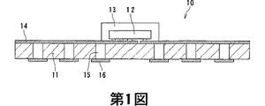
第1図は、本発明に係る発光装置の一実施例を示す断面図である。
第2図は、第1図に示す発光装置の平面図である。
第3図は、実施例1および比較例1〜2に係る発光装置における通電電流値と発光光度との関係を示すグラフである。
第4図は、従来の発光装置の構成例を示す断面図である。
第5図(a)、(b)はそれぞれレジスト膜を形成した発光装置の構成例を示す平面図および断面図である。
第6図(a)、(b)はそれぞれレジスト膜を形成しない発光装置の構成例を示す平面図および断面図である。
第7図は、第5図および第6図に示す発光装置における通電電流値と発光光度との関係を示すグラフである。FIG. 1 is a sectional view showing an embodiment of a light emitting device according to the present invention.
FIG. 2 is a plan view of the light emitting device shown in FIG.
FIG. 3 is a graph showing the relationship between the energization current value and the luminous intensity in the light emitting devices according to Example 1 and Comparative Examples 1 and 2.
FIG. 4 is a cross-sectional view showing a configuration example of a conventional light emitting device.
FIGS. 5A and 5B are a plan view and a cross-sectional view showing a configuration example of a light emitting device in which a resist film is formed.
FIGS. 6A and 6B are a plan view and a cross-sectional view, respectively, showing a configuration example of a light emitting device in which a resist film is not formed.
FIG. 7 is a graph showing the relationship between the energization current value and the luminous intensity in the light emitting device shown in FIGS. 5 and 6.
次に本発明に係る発光装置の実施形態について添付図面を参照してより具体的に説明する。
[実施例1〜24および比較例1〜11]
各実施例用および比較例用の基板として、表1に示すような厚さおよび熱伝導率を有する窒化アルミニウム(AlN)基板,エポキシ樹脂基板およびアルミナ(Al2O3)基板を多数用意した。各実施例用の窒化アルミニウム(AlN)基板および比較例用のアルミナ(Al2O3)基板は、同時焼成法によって製造されたものであり、基板の厚さ方向に貫通するビアホールが形成されていると共に、ビアホールの基板裏面側の端部には部品のリードを接合するための端子導体部分としてのランドが形成されている。
次に、窒化アルミニウム(AlN)基板およびアルミナ(Al2O3)基板の発光素子としてのLEDチップが搭載される表面が表1に示すように0.1〜0.3μmRaの表面粗さを有するように鏡面研摩した。さらに、発光素子としてのLEDチップの周囲となる基板表面に、表1に示す厚さで銀(Ag)またはアルミニウム(Al)から成る金属蒸着膜を化学蒸着法によって形成した。
一方、比較例1においては、エポキシ樹脂基板を使用し金属蒸着膜は形成していない。また、比較例2〜3においては、熱伝導率が低いアルミナ(Al2O3)基板のチップ搭載部周辺の基板表面にAgまたはAlから成る金属蒸着膜を形成したものである。さらに、比較例4〜11は、焼結後に基板表面に残る付着物を除去する程度に軽く研摩することによりLEDチップ搭載面の表面粗さを、本発明で規定する値よりも過大に調整した以外は実施例1と同様の工程で調製したものである。
さらに、上記各基板表面に同一仕様の青色発光LEDチップを搭載し、基板背面(裏面)側のランドに通電端子を接合し、ビアホールを介してLEDチップに通電するように配線を接続した。最後に、搭載したLEDチップを覆うように黄色発光蛍光体(YAG)を装着することにより、白色光を発する各実施例および比較例に係る発光装置を製造した。
こうして調製された各実施例に係る発光装置10は、第1図および第2図に示すように、熱伝導率が高い窒化アルミニウム(AlN)基板11と、このAlN基板11の表面に搭載された青色発光LEDチップ12と、このLEDチップ12表面を覆うように装着された黄色発光蛍光体13と、上記AlN基板11の表面に形成された金属蒸着膜14と、AlN基板11を厚さ方向に貫通するように形成されたビアホール15と、このビアホール15の、基板背面側の端部に形成されたランド16とを備え、AlN基板11の背面(裏面)側のランド16に通電端子を接合し、ビアホール15を介してLEDチップ12に通電するように配線を接続した構造を有する。
上記のように調製した各実施例および比較例に係る発光装置について、各基板の仕様(材料種類、厚さ、熱伝導率)、LEDチップ搭載面の表面粗さ、金属蒸着膜の仕様(種類、厚さ、光反射率)をまとめるとともに、各LEDチップへの通電量を徐々に増加せしめ、LEDチップが破壊されずに安定的に発光する範囲で最大の電流値を測定した。また、各発光装置における最大の発光強度を測定して表1に示す結果を得た。なお、発光強度はアルミナ(Al2O3)基板を使用した比較例2に係る発光装置の発光強度を100%(基準値)として相対的に表示した。

一方、LEDチップ12の搭載基板として、熱伝導率が低いエポキシ樹脂基板やアルミナ(Al2O3)基板を使用した比較例1〜3に係る発光装置においては、放熱性が低いために通電可能な電力が制限されるため、最大電流値は相対的に低く発光強度についての改善も期待できないことが再確認できた。また、AlN基板を用いてもLEDチップ搭載面の表面粗さが過大である比較例4〜11においては、通電可能な電流値は高いが、チップの接合面における光の乱反射・吸収が多くなり、発光がAlN基板へ吸収される割合が増加するため発光強度が低下した。
第3図は実施例1および比較例1〜2に係る発光装置における通電電流値と発光光度関係を示すグラフである。LEDチップ12の搭載基板として、窒化アルミニウム(AlN)基板11を使用した実施例1に係る発光装置は、樹脂基板やアルミナ(Al2O3)基板を使用した比較例1,2に係る発光装置と比較して、通電可能な最大電流値を大幅に増加させることができ、発光光度を飛躍的に高めることが可能になった。
上記各実施例に係る発光装置10によれば、青色発光LEDチップ12を搭載する基板(LED用パッケージ)として、熱伝導率が高い窒化アルミニウム(AlN)のコファイア基板(同時焼成基板)11を使用しているため、発光装置10の放熱性が大幅に高まり、通電限界量が増大し大電流を流すことが可能になるために、発光輝度を大幅に高くすることが可能になる。
また、発光素子としての青色発光LEDチップ12が搭載されるAlN基板11の表面が鏡面研摩されているために、研摩面での反射率が高くなりLEDチップ12の接合面側からの発光が効果的に基板表面側に反射され、発光強度(輝度)を実質的に上昇させることができる。
さらに、LEDチップ12が搭載される窒化アルミニウム基板11の表面と裏面とを貫通しLEDチップ12に裏面から導通させるためのビアホール15が形成され、LEDチップ12への通電は窒化アルミニウム基板11の裏面からこのビアホール15を介して表面側のLEDチップ12になされるため、基板11の表面側においてワイヤボンディング法によって配線を接続する必要がなく、配線構造が簡素化される上に、ボンディングワイヤの厚さ方向への突出がないため、発光装置10を薄く小型に形成できる。
また、窒化アルミニウム基板11の表面と裏面とを貫通しLEDチップ12に裏面から導通させるためのビアホール15が形成されているため、LEDチップ12をフリップチップ法によりフェイスダウン方式による配線が可能になる。このフェイスダウン方式による配線構造によれば、LEDチップ12表面の任意の位置から電極を取り出すことが可能であるため、LEDチップ12と配線導体とが最短距離で接続可能である上に、電極数が増加しても発光素子としてのLEDチップのサイズが大型化せず、しかも超薄型実装も可能になる。
次に、導電層パターン間など、金属蒸着膜が形成されている領域以外で窒化アルミニウム基板の表面が露出している部位に白色のレジスト膜を塗布した発光装置の実施形態について説明する。Next, an embodiment of a light emitting device according to the present invention will be described more specifically with reference to the accompanying drawings.
[Examples 1 to 24 and Comparative Examples 1 to 11]
A large number of aluminum nitride (AlN) substrates, epoxy resin substrates, and alumina (Al 2 O 3 ) substrates having thicknesses and thermal conductivities as shown in Table 1 were prepared as substrates for the examples and comparative examples. The aluminum nitride (AlN) substrate for each example and the alumina (Al 2 O 3 ) substrate for comparative example are manufactured by a co-firing method, and a via hole penetrating in the thickness direction of the substrate is formed. In addition, a land as a terminal conductor portion for joining component leads is formed at the end of the via hole on the back side of the substrate.
Next, as shown in Table 1, the surface on which the LED chips as the light emitting elements of the aluminum nitride (AlN) substrate and the alumina (Al 2 O 3 ) substrate are mounted has a surface roughness of 0.1 to 0.3 μmRa. Mirror surface was polished as follows. Further, a metal vapor deposition film made of silver (Ag) or aluminum (Al) with a thickness shown in Table 1 was formed on the substrate surface around the LED chip as the light emitting element by a chemical vapor deposition method.
On the other hand, in Comparative Example 1, an epoxy resin substrate is used and a metal vapor deposition film is not formed. In Comparative Examples 2 to 3, a metal vapor deposition film made of Ag or Al is formed on the surface of the substrate around the chip mounting portion of the alumina (Al 2 O 3 ) substrate having low thermal conductivity. Further, in Comparative Examples 4 to 11, the surface roughness of the LED chip mounting surface was adjusted to be larger than the value specified in the present invention by lightly polishing to such an extent that the deposits remaining on the substrate surface after sintering were removed. Other than that, it was prepared in the same process as in Example 1.
Furthermore, the blue light emitting LED chip of the same specification was mounted on the surface of each said board | substrate, the electricity supply terminal was joined to the land of the board back surface (back surface) side, and the wiring was connected so that it might supply with electricity to a LED chip through a via hole. Finally, by attaching a yellow light emitting phosphor (YAG) so as to cover the mounted LED chip, the light emitting devices according to the respective examples and comparative examples emitting white light were manufactured.
As shown in FIGS. 1 and 2, the
About the light emitting device according to each of the examples and comparative examples prepared as described above, the specifications of each substrate (material type, thickness, thermal conductivity), the surface roughness of the LED chip mounting surface, the specifications of the metal vapor deposition film (type) , Thickness, and light reflectance), the amount of current supplied to each LED chip was gradually increased, and the maximum current value was measured in a range in which the LED chip could stably emit light without being destroyed. Moreover, the maximum light emission intensity in each light-emitting device was measured, and the results shown in Table 1 were obtained. The light emission intensity was relatively displayed with the light emission intensity of the light emitting device according to Comparative Example 2 using an alumina (Al 2 O 3 ) substrate as 100% (reference value).
On the other hand, in the light emitting devices according to Comparative Examples 1 to 3 using an epoxy resin substrate or an alumina (Al 2 O 3 ) substrate having a low thermal conductivity as a mounting substrate for the
FIG. 3 is a graph showing the relationship between the current value and the luminous intensity in the light emitting devices according to Example 1 and Comparative Examples 1 and 2. The light emitting device according to Example 1 using the aluminum nitride (AlN)
According to the
Further, since the surface of the
Furthermore, a via
Further, since the via
Next, an embodiment of a light emitting device in which a white resist film is applied to a portion where the surface of the aluminum nitride substrate is exposed in a region other than the region where the metal vapor deposition film is formed, such as between conductive layer patterns, will be described.
第5図(a)、(b)で示すように、実施例1で調製した発光装置で導電層となる金属蒸着膜14、14間に形成される隙間(パターン間ギャップ)17に、白色のソルダーレジストインクをスクリーン印刷によって塗布印刷して白色レジスト膜18を形成した。しかる後に、フリップチップ用バンプ19を介して発光素子としてのLEDチップ12を金属蒸着膜14上に搭載固定することにより、実施例25に係る発光装置を製造した。
[比較例12]
一方、第6図(a)、(b)で示すように、金属蒸着膜14、14間に形成される隙間17に、白色レジスト膜を形成しない点以外は、上記実施例25と同様に処理し、フリップチップ用バンプ19を介してLEDチップ12を金属蒸着膜14上に搭載固定することにより、比較例12に係る発光装置を製造した。
こうして調製した実施例25および比較例12に係る発光装置に通電量を徐々に増加させた時の発光光度の経時変化を測定し第7図に示す結果を得た。
第7図に示す結果から明らかなように、金属蒸着膜14、14間に形成される隙間17に白色レジスト膜18を形成した実施例25に係る発光装置においては、白色レジスト膜18の反射・遮蔽効果によりAlN基板の裏面方向への光の逸散が効果的に抑制されており、定格電流範囲における発光強度を、比較例12と比較して28〜32%程度も向上できることが実証された。
一方、白色レジスト膜を形成しない比較例12に係る発光装置においては、第6図(b)に示すように、LEDチップ12からの発光が隙間17から矢印で示すようにAlN基板11の背面側に逸散するために、発光光度が相対的に低下した。As shown in FIGS. 5 (a) and 5 (b), the gap (interpattern gap) 17 formed between the metal vapor-deposited
[Comparative Example 12]
On the other hand, as shown in FIGS. 6 (a) and 6 (b), the same treatment as in Example 25 was performed except that a white resist film was not formed in the
The time-dependent change of the luminous intensity when the energization amount was gradually increased in the light emitting devices according to Example 25 and Comparative Example 12 thus prepared was measured, and the results shown in FIG. 7 were obtained.
As is apparent from the results shown in FIG. 7, in the light emitting device according to Example 25 in which the white resist
On the other hand, in the light emitting device according to Comparative Example 12 in which the white resist film is not formed, as shown in FIG. 6 (b), the light emission from the
上記構成に係る発光装置によれば、LEDチップを搭載する基板(LED用パッケージ)として、熱伝導率が高い窒化アルミニウム(AlN)のコファイア(co−fire)基板(同時焼成基板)を使用しているため、発光装置の放熱性が大幅に高まり、通電限界量が増大し大電流を流すことが可能になるために、発光輝度を大幅に高くすることが可能になる。
また、発光素子が搭載される基板表面が鏡面研摩されているために、研摩面での反射率が高くなり発光素子の接合面側からの発光が効果的に基板表面側に反射され、発光強度(輝度)を実質的に上昇させることができる。
さらに、窒化アルミニウム基板表面の発光素子の搭載部に、発光素子からの発光の反射率が90%以上である金属蒸着膜が形成されているために、光の反射強度を高めることができる。
さらに、発光素子が搭載される窒化アルミニウム基板の表面と裏面とを貫通し発光素子に裏面から導通させるためのビアホールが形成され、発光素子への通電は窒化アルミニウム基板の裏面からこのビアホールを介して表面側の発光素子になされるため、基板の表面側においてワイヤボンディング法によって配線を接続する必要がなく、配線構造が簡素化される上に、ボンディングワイヤの厚さ方向への突出がないため、発光装置を薄く小型に形成できる。
また、窒化アルミニウム基板の表面と裏面とを貫通し発光素子に裏面から導通させるためのビアホールが形成されているため、発光素子をフリップチップ法によりフェイスダウン方式による配線が可能になる。このフェイスダウン方式による配線構造によれば、発光素子表面の任意の位置から電極を取り出すことが可能であるため、発光素子と配線導体とが最短距離で接続可能である上に、電極数が増加しても発光素子としてのLEDチップのサイズが大型化せず、しかも超薄型実装も可能になる。
さらに、導電層パターン間など、金属蒸着膜が形成されている領域以外で窒化アルミニウム基板の表面が露出している部位に白色のレジスト膜を塗布することにより、光の反射強度をさらに高めることが可能になる。According to the light emitting device according to the above configuration, an aluminum nitride (AlN) co-fire substrate (co-fired substrate) with high thermal conductivity is used as a substrate (LED package) on which an LED chip is mounted. Therefore, the heat dissipation of the light-emitting device is significantly increased, the amount of energization is increased, and a large current can be passed, so that the light emission luminance can be significantly increased.
In addition, since the surface of the substrate on which the light emitting element is mounted is mirror-polished, the reflectance on the polished surface is increased, and light emitted from the bonding surface side of the light emitting element is effectively reflected to the substrate surface side, and the light emission intensity. (Luminance) can be substantially increased.
Furthermore, since a metal vapor deposition film having a reflectance of light emission from the light emitting element of 90% or more is formed on the mounting portion of the light emitting element on the surface of the aluminum nitride substrate, the light reflection intensity can be increased.
Furthermore, a via hole is formed through the front and back surfaces of the aluminum nitride substrate on which the light-emitting element is mounted, and the light-emitting element is electrically connected to the light-emitting element from the back surface. Because it is a light emitting element on the surface side, it is not necessary to connect wiring by the wire bonding method on the surface side of the substrate, the wiring structure is simplified, and there is no protrusion in the thickness direction of the bonding wire, The light emitting device can be formed thin and small.
In addition, since a via hole is formed through the front and back surfaces of the aluminum nitride substrate to allow the light emitting element to conduct from the back surface, the light emitting element can be wired in a face-down manner by a flip chip method. According to this face-down wiring structure, the electrodes can be taken out from any position on the surface of the light emitting element, so that the light emitting element and the wiring conductor can be connected at the shortest distance, and the number of electrodes increases. Even so, the size of the LED chip as the light emitting element does not increase, and ultra-thin mounting is possible.
Furthermore, by applying a white resist film on the exposed portion of the surface of the aluminum nitride substrate other than the region where the metal deposition film is formed, such as between conductive layer patterns, the light reflection intensity can be further increased. It becomes possible.
Claims (7)
Priority Applications (1)
| Application Number | Priority Date | Filing Date | Title |
|---|---|---|---|
| JP2005514318A JP4817845B2 (en) | 2003-09-30 | 2004-09-29 | Method for manufacturing light emitting device |
Applications Claiming Priority (4)
| Application Number | Priority Date | Filing Date | Title |
|---|---|---|---|
| JP2003341016 | 2003-09-30 | ||
| JP2003341016 | 2003-09-30 | ||
| JP2005514318A JP4817845B2 (en) | 2003-09-30 | 2004-09-29 | Method for manufacturing light emitting device |
| PCT/JP2004/014686 WO2005031882A1 (en) | 2003-09-30 | 2004-09-29 | Light emitting device |
Related Child Applications (1)
| Application Number | Title | Priority Date | Filing Date |
|---|---|---|---|
| JP2007189139A Division JP4818215B2 (en) | 2003-09-30 | 2007-07-20 | Light emitting device |
Publications (2)
| Publication Number | Publication Date |
|---|---|
| JPWO2005031882A1 true JPWO2005031882A1 (en) | 2006-12-07 |
| JP4817845B2 JP4817845B2 (en) | 2011-11-16 |
Family
ID=34386216
Family Applications (2)
| Application Number | Title | Priority Date | Filing Date |
|---|---|---|---|
| JP2005514318A Expired - Lifetime JP4817845B2 (en) | 2003-09-30 | 2004-09-29 | Method for manufacturing light emitting device |
| JP2007189139A Expired - Fee Related JP4818215B2 (en) | 2003-09-30 | 2007-07-20 | Light emitting device |
Family Applications After (1)
| Application Number | Title | Priority Date | Filing Date |
|---|---|---|---|
| JP2007189139A Expired - Fee Related JP4818215B2 (en) | 2003-09-30 | 2007-07-20 | Light emitting device |
Country Status (7)
| Country | Link |
|---|---|
| US (1) | US8610145B2 (en) |
| EP (1) | EP1670073B1 (en) |
| JP (2) | JP4817845B2 (en) |
| KR (1) | KR100808705B1 (en) |
| CN (1) | CN100442551C (en) |
| TW (1) | TWI253767B (en) |
| WO (1) | WO2005031882A1 (en) |
Cited By (2)
| Publication number | Priority date | Publication date | Assignee | Title |
|---|---|---|---|---|
| JP2008219333A (en) * | 2007-03-02 | 2008-09-18 | Rohm Co Ltd | Linear light source device |
| JP2013041867A (en) * | 2011-08-11 | 2013-02-28 | Citizen Electronics Co Ltd | Light emitting diode |
Families Citing this family (68)
| Publication number | Priority date | Publication date | Assignee | Title |
|---|---|---|---|---|
| US9142734B2 (en) | 2003-02-26 | 2015-09-22 | Cree, Inc. | Composite white light source and method for fabricating |
| CN100502062C (en) | 2003-04-30 | 2009-06-17 | 美商克立股份有限公司 | High power light emitter package with compact optical element |
| US7915085B2 (en) | 2003-09-18 | 2011-03-29 | Cree, Inc. | Molded chip fabrication method |
| US7812360B2 (en) | 2004-10-04 | 2010-10-12 | Kabushiki Kaisha Toshiba | Light emitting device, lighting equipment or liquid crystal display device using such light emitting device |
| JP4835917B2 (en) * | 2005-10-25 | 2011-12-14 | 日立化成工業株式会社 | WIRING BOARD FOR LIGHT EMITTING ELEMENT AND LIGHT EMITTING DEVICE USING THE SAME |
| JP5073946B2 (en) * | 2005-12-27 | 2012-11-14 | 新光電気工業株式会社 | Semiconductor device and manufacturing method of semiconductor device |
| JP4049186B2 (en) | 2006-01-26 | 2008-02-20 | ソニー株式会社 | Light source device |
| JP2007234968A (en) * | 2006-03-02 | 2007-09-13 | Nichia Chem Ind Ltd | LIGHT EMITTING DEVICE MANUFACTURING METHOD AND LIGHT EMITTING DEVICE |
| KR100791594B1 (en) | 2006-08-31 | 2008-01-03 | 원광대학교산학협력단 | Lighting device with a heat radiating part |
| JP2010512662A (en) | 2006-12-11 | 2010-04-22 | ザ リージェンツ オブ ザ ユニバーシティ オブ カリフォルニア | Transparent light emitting diode |
| KR100845856B1 (en) * | 2006-12-21 | 2008-07-14 | 엘지전자 주식회사 | Light emitting device package and its manufacturing method |
| US9159888B2 (en) | 2007-01-22 | 2015-10-13 | Cree, Inc. | Wafer level phosphor coating method and devices fabricated utilizing method |
| TWI338387B (en) * | 2007-05-28 | 2011-03-01 | Delta Electronics Inc | Current spreading layer with micro/nano structure, light-emitting diode apparatus and its manufacturing method |
| US8441018B2 (en) | 2007-08-16 | 2013-05-14 | The Trustees Of Columbia University In The City Of New York | Direct bandgap substrates and methods of making and using |
| US9660153B2 (en) | 2007-11-14 | 2017-05-23 | Cree, Inc. | Gap engineering for flip-chip mounted horizontal LEDs |
| US9754926B2 (en) | 2011-01-31 | 2017-09-05 | Cree, Inc. | Light emitting diode (LED) arrays including direct die attach and related assemblies |
| US9640737B2 (en) | 2011-01-31 | 2017-05-02 | Cree, Inc. | Horizontal light emitting diodes including phosphor particles |
| CN101459211B (en) * | 2007-12-11 | 2011-03-02 | 富士迈半导体精密工业(上海)有限公司 | Solid illuminating device |
| US9431589B2 (en) | 2007-12-14 | 2016-08-30 | Cree, Inc. | Textured encapsulant surface in LED packages |
| US9041285B2 (en) | 2007-12-14 | 2015-05-26 | Cree, Inc. | Phosphor distribution in LED lamps using centrifugal force |
| US8878219B2 (en) * | 2008-01-11 | 2014-11-04 | Cree, Inc. | Flip-chip phosphor coating method and devices fabricated utilizing method |
| US9035253B2 (en) | 2008-06-27 | 2015-05-19 | Panasonic Intellectual Property Managment Co., Ltd. | Infrared sensor element |
| CN102077376B (en) * | 2008-06-27 | 2015-04-22 | 松下电器产业株式会社 | Piezoelectric element and its manufacturing method |
| JP5334483B2 (en) * | 2008-07-24 | 2013-11-06 | 京セラ株式会社 | LIGHT EMITTING DEVICE AND LIGHTING DEVICE USING LIGHT EMITTING DEVICE |
| TW201011936A (en) * | 2008-09-05 | 2010-03-16 | Advanced Optoelectronic Tech | Light emitting device and fabrication thereof |
| US8567988B2 (en) * | 2008-09-29 | 2013-10-29 | Bridgelux, Inc. | Efficient LED array |
| JP2011165833A (en) | 2010-02-08 | 2011-08-25 | Toshiba Corp | Led module |
| US10546846B2 (en) | 2010-07-23 | 2020-01-28 | Cree, Inc. | Light transmission control for masking appearance of solid state light sources |
| CN102054914B (en) * | 2010-11-09 | 2013-09-04 | 映瑞光电科技(上海)有限公司 | Light emitting diode and manufacturing method thereof and light emitting device |
| CN102054913B (en) | 2010-11-09 | 2013-07-10 | 映瑞光电科技(上海)有限公司 | LED as well as manufacturing method and light-emitting device thereof |
| US9300062B2 (en) | 2010-11-22 | 2016-03-29 | Cree, Inc. | Attachment devices and methods for light emitting devices |
| US9490235B2 (en) | 2010-11-22 | 2016-11-08 | Cree, Inc. | Light emitting devices, systems, and methods |
| JP2012134471A (en) * | 2010-11-30 | 2012-07-12 | Fujifilm Corp | Insulating substrate and manufacturing method thereof |
| JP2014041851A (en) * | 2010-12-24 | 2014-03-06 | Asahi Glass Co Ltd | Coupling substrate and method for manufacturing the same, element substrate and light emitting device |
| JP2012151191A (en) * | 2011-01-17 | 2012-08-09 | Ibiden Co Ltd | Wiring board for led, light emitting module, manufacturing method of the wiring board for the led, and manufacturing method of the light emitting module |
| US20120188738A1 (en) * | 2011-01-25 | 2012-07-26 | Conexant Systems, Inc. | Integrated led in system-in-package module |
| US9673363B2 (en) * | 2011-01-31 | 2017-06-06 | Cree, Inc. | Reflective mounting substrates for flip-chip mounted horizontal LEDs |
| US9166126B2 (en) | 2011-01-31 | 2015-10-20 | Cree, Inc. | Conformally coated light emitting devices and methods for providing the same |
| US9831220B2 (en) | 2011-01-31 | 2017-11-28 | Cree, Inc. | Light emitting diode (LED) arrays including direct die attach and related assemblies |
| US9053958B2 (en) * | 2011-01-31 | 2015-06-09 | Cree, Inc. | Light emitting diode (LED) arrays including direct die attach and related assemblies |
| US9401103B2 (en) | 2011-02-04 | 2016-07-26 | Cree, Inc. | LED-array light source with aspect ratio greater than 1 |
| KR20140097284A (en) | 2011-11-07 | 2014-08-06 | 크리,인코포레이티드 | High voltage array light emitting diode(led) devices, fixtures and methods |
| US10043960B2 (en) | 2011-11-15 | 2018-08-07 | Cree, Inc. | Light emitting diode (LED) packages and related methods |
| US10134961B2 (en) | 2012-03-30 | 2018-11-20 | Cree, Inc. | Submount based surface mount device (SMD) light emitter components and methods |
| US9735198B2 (en) | 2012-03-30 | 2017-08-15 | Cree, Inc. | Substrate based light emitter devices, components, and related methods |
| US10439112B2 (en) * | 2012-05-31 | 2019-10-08 | Cree, Inc. | Light emitter packages, systems, and methods having improved performance |
| US9349929B2 (en) | 2012-05-31 | 2016-05-24 | Cree, Inc. | Light emitter packages, systems, and methods |
| USD749051S1 (en) | 2012-05-31 | 2016-02-09 | Cree, Inc. | Light emitting diode (LED) package |
| JP5835133B2 (en) | 2012-07-10 | 2015-12-24 | 豊田合成株式会社 | LED mounting substrate and manufacturing method thereof |
| KR101382363B1 (en) * | 2012-08-28 | 2014-04-08 | 주식회사 아모센스 | Method for manufacturing led package having varistor substrate and led package having varistor substrate thereby |
| KR101428774B1 (en) * | 2013-04-30 | 2014-08-12 | 주식회사 세미콘라이트 | Semiconductor light emitting device and manufacturing method of the same |
| CN104241262B (en) | 2013-06-14 | 2020-11-06 | 惠州科锐半导体照明有限公司 | Light emitting device and display device |
| JP6181492B2 (en) * | 2013-09-20 | 2017-08-16 | 京セラ株式会社 | Light emitting device |
| CN204717393U (en) * | 2014-11-19 | 2015-10-21 | 魏晓敏 | LED modules and LED equipment |
| CN104600047B (en) * | 2014-12-26 | 2017-11-14 | 珠海格力电器股份有限公司 | Power module and packaging method thereof |
| CN105280797A (en) * | 2015-05-28 | 2016-01-27 | 江苏欧密格光电科技股份有限公司 | LED bonding pad conversion module |
| JP6771180B2 (en) * | 2016-05-27 | 2020-10-21 | パナソニックIpマネジメント株式会社 | Light source module and lighting device |
| USD823492S1 (en) | 2016-10-04 | 2018-07-17 | Cree, Inc. | Light emitting device |
| CN106324946A (en) * | 2016-10-31 | 2017-01-11 | 维沃移动通信有限公司 | Heat dissipation device for flash lamp |
| JP6798455B2 (en) | 2017-08-31 | 2020-12-09 | 豊田合成株式会社 | Manufacturing method of light emitting device |
| US20190267525A1 (en) * | 2018-02-26 | 2019-08-29 | Semicon Light Co., Ltd. | Semiconductor Light Emitting Devices And Method Of Manufacturing The Same |
| TWI684293B (en) * | 2018-06-29 | 2020-02-01 | 同泰電子科技股份有限公司 | Backlight circuit board structure with high reflectivity and method for making thereof |
| US10683988B2 (en) | 2018-10-04 | 2020-06-16 | Elemental LED, Inc. | Mirrored LED lighting |
| TWM579383U (en) | 2018-12-25 | 2019-06-11 | 同泰電子科技股份有限公司 | Substrate structure with high reflectivity |
| US11592166B2 (en) | 2020-05-12 | 2023-02-28 | Feit Electric Company, Inc. | Light emitting device having improved illumination and manufacturing flexibility |
| US11876042B2 (en) | 2020-08-03 | 2024-01-16 | Feit Electric Company, Inc. | Omnidirectional flexible light emitting device |
| CN113880044A (en) * | 2021-08-20 | 2022-01-04 | 北京强度环境研究所 | Thin film sensor lead connecting method |
| CN114334927B (en) * | 2021-12-29 | 2025-05-02 | 华引芯(武汉)科技有限公司 | Light emitting device and light emitting apparatus |
Citations (6)
| Publication number | Priority date | Publication date | Assignee | Title |
|---|---|---|---|---|
| JPH02190859A (en) * | 1989-01-20 | 1990-07-26 | Fuji Photo Film Co Ltd | Liquid photosensitive resin composition |
| JPH09293904A (en) * | 1996-04-26 | 1997-11-11 | Nichia Chem Ind Ltd | LED package |
| JPH10279377A (en) * | 1997-04-04 | 1998-10-20 | Tokuyama Corp | Metallized composition and method for manufacturing aluminum nitride substrate using the same |
| EP1059667A2 (en) * | 1999-06-09 | 2000-12-13 | Sanyo Electric Co., Ltd. | Hybrid integrated circuit device |
| JP2001338505A (en) * | 2000-05-26 | 2001-12-07 | Matsushita Electric Works Ltd | Lighting equipment |
| JP2003023183A (en) * | 2001-07-06 | 2003-01-24 | Stanley Electric Co Ltd | Surface mount type LED lamp |
Family Cites Families (20)
| Publication number | Priority date | Publication date | Assignee | Title |
|---|---|---|---|---|
| JPS54158661A (en) * | 1978-06-01 | 1979-12-14 | Tokyo Purinto Kougiyou Kk | Printed circuit board |
| JPS62128576A (en) | 1985-11-29 | 1987-06-10 | Hamamatsu Photonics Kk | Light emitting diode |
| US5124234A (en) * | 1989-01-20 | 1992-06-23 | Fuji Photo Film Co., Ltd. | Liquid light-sensitive resin composition |
| JPH0617226A (en) * | 1992-05-07 | 1994-01-25 | Nkk Corp | Mirror reflector with excellent workability and scratch resistance |
| JP3165779B2 (en) * | 1995-07-18 | 2001-05-14 | 株式会社トクヤマ | Submount |
| TW383508B (en) * | 1996-07-29 | 2000-03-01 | Nichia Kagaku Kogyo Kk | Light emitting device and display |
| JP3316838B2 (en) * | 1997-01-31 | 2002-08-19 | 日亜化学工業株式会社 | Light emitting device |
| US5886401A (en) * | 1997-09-02 | 1999-03-23 | General Electric Company | Structure and fabrication method for interconnecting light emitting diodes with metallization extending through vias in a polymer film overlying the light emitting diodes |
| JPH11220178A (en) * | 1998-01-30 | 1999-08-10 | Rohm Co Ltd | Semiconductor light-emitting device |
| US6184544B1 (en) * | 1998-01-29 | 2001-02-06 | Rohm Co., Ltd. | Semiconductor light emitting device with light reflective current diffusion layer |
| TW456004B (en) * | 1998-02-10 | 2001-09-21 | Nissha Printing | Substrate sheet for semiconductor module, method and apparatus for manufacturing the same |
| US6274924B1 (en) * | 1998-11-05 | 2001-08-14 | Lumileds Lighting, U.S. Llc | Surface mountable LED package |
| US6614103B1 (en) * | 2000-09-01 | 2003-09-02 | General Electric Company | Plastic packaging of LED arrays |
| JP4248173B2 (en) * | 2000-12-04 | 2009-04-02 | 株式会社東芝 | Aluminum nitride substrate and thin film substrate using the same |
| JP5110744B2 (en) | 2000-12-21 | 2012-12-26 | フィリップス ルミレッズ ライティング カンパニー リミテッド ライアビリティ カンパニー | Light emitting device and manufacturing method thereof |
| US6758607B2 (en) * | 2001-03-09 | 2004-07-06 | Sumitomo Electric Industries, Ltd. | Optical communication module and optical communication module product |
| JP2002335020A (en) * | 2001-05-10 | 2002-11-22 | Nichia Chem Ind Ltd | Light emitting device |
| JP2003100921A (en) * | 2001-09-25 | 2003-04-04 | Kyocera Corp | Container for storing optical semiconductor elements |
| US20040188696A1 (en) * | 2003-03-28 | 2004-09-30 | Gelcore, Llc | LED power package |
| US7256486B2 (en) * | 2003-06-27 | 2007-08-14 | Avago Technologies Ecbu Ip (Singapore) Pte. Ltd. | Packaging device for semiconductor die, semiconductor device incorporating same and method of making same |
-
2004
- 2004-09-29 US US10/572,595 patent/US8610145B2/en active Active
- 2004-09-29 WO PCT/JP2004/014686 patent/WO2005031882A1/en not_active Ceased
- 2004-09-29 CN CNB2004800282708A patent/CN100442551C/en not_active Expired - Lifetime
- 2004-09-29 JP JP2005514318A patent/JP4817845B2/en not_active Expired - Lifetime
- 2004-09-29 EP EP04773617.8A patent/EP1670073B1/en not_active Expired - Lifetime
- 2004-09-29 KR KR1020067006183A patent/KR100808705B1/en not_active Expired - Lifetime
- 2004-09-30 TW TW093129685A patent/TWI253767B/en not_active IP Right Cessation
-
2007
- 2007-07-20 JP JP2007189139A patent/JP4818215B2/en not_active Expired - Fee Related
Patent Citations (6)
| Publication number | Priority date | Publication date | Assignee | Title |
|---|---|---|---|---|
| JPH02190859A (en) * | 1989-01-20 | 1990-07-26 | Fuji Photo Film Co Ltd | Liquid photosensitive resin composition |
| JPH09293904A (en) * | 1996-04-26 | 1997-11-11 | Nichia Chem Ind Ltd | LED package |
| JPH10279377A (en) * | 1997-04-04 | 1998-10-20 | Tokuyama Corp | Metallized composition and method for manufacturing aluminum nitride substrate using the same |
| EP1059667A2 (en) * | 1999-06-09 | 2000-12-13 | Sanyo Electric Co., Ltd. | Hybrid integrated circuit device |
| JP2001338505A (en) * | 2000-05-26 | 2001-12-07 | Matsushita Electric Works Ltd | Lighting equipment |
| JP2003023183A (en) * | 2001-07-06 | 2003-01-24 | Stanley Electric Co Ltd | Surface mount type LED lamp |
Cited By (2)
| Publication number | Priority date | Publication date | Assignee | Title |
|---|---|---|---|---|
| JP2008219333A (en) * | 2007-03-02 | 2008-09-18 | Rohm Co Ltd | Linear light source device |
| JP2013041867A (en) * | 2011-08-11 | 2013-02-28 | Citizen Electronics Co Ltd | Light emitting diode |
Also Published As
| Publication number | Publication date |
|---|---|
| EP1670073B1 (en) | 2014-07-02 |
| KR20060083984A (en) | 2006-07-21 |
| JP2007266647A (en) | 2007-10-11 |
| CN1860620A (en) | 2006-11-08 |
| EP1670073A4 (en) | 2008-07-02 |
| TW200522394A (en) | 2005-07-01 |
| JP4817845B2 (en) | 2011-11-16 |
| EP1670073A1 (en) | 2006-06-14 |
| US20070200128A1 (en) | 2007-08-30 |
| US8610145B2 (en) | 2013-12-17 |
| CN100442551C (en) | 2008-12-10 |
| WO2005031882A1 (en) | 2005-04-07 |
| JP4818215B2 (en) | 2011-11-16 |
| KR100808705B1 (en) | 2008-02-29 |
| TWI253767B (en) | 2006-04-21 |
Similar Documents
| Publication | Publication Date | Title |
|---|---|---|
| JP4818215B2 (en) | Light emitting device | |
| JP4960099B2 (en) | Light emitting device and lighting apparatus or liquid crystal display device using the same | |
| JP4675906B2 (en) | Light-emitting element mounting substrate, light-emitting element storage package, light-emitting device, and lighting device | |
| CN100448037C (en) | Semiconductor light emitting device | |
| KR100620844B1 (en) | Light-emitting apparatus and illuminating apparatus | |
| TWI389295B (en) | Light-emitting diode light source module | |
| CN100539134C (en) | Lighting device | |
| CN105103313B (en) | Light-emitting element package | |
| WO2002089221A1 (en) | Light emitting device comprising led chip | |
| JP2008251663A (en) | Light emitting device and lighting device | |
| KR100851183B1 (en) | Semiconductor light emitting device package | |
| JP2005039194A (en) | Light emitting element storage package, light emitting device, and lighting device | |
| JP2008091459A (en) | Led illumination apparatus and manufacturing method thereof | |
| US9897298B2 (en) | Light emitting module and light unit having the same | |
| JP2005150408A (en) | Light emitting device mounting package and light source device | |
| KR100645657B1 (en) | White light emitting diode module with flip chip printed circuit board and flip chip printed circuit board | |
| JP2007208292A (en) | Light emitting device | |
| TW201133960A (en) | Light-emitting module and method for manufacturing same | |
| JP2005039193A (en) | Light emitting element storage package, light emitting device, and lighting device | |
| JP4480736B2 (en) | Light emitting device | |
| KR102024296B1 (en) | Light emitting device package |
Legal Events
| Date | Code | Title | Description |
|---|---|---|---|
| A621 | Written request for application examination |
Free format text: JAPANESE INTERMEDIATE CODE: A621 Effective date: 20070914 |
|
| A131 | Notification of reasons for refusal |
Free format text: JAPANESE INTERMEDIATE CODE: A131 Effective date: 20101109 |
|
| A521 | Request for written amendment filed |
Free format text: JAPANESE INTERMEDIATE CODE: A523 Effective date: 20110111 |
|
| A02 | Decision of refusal |
Free format text: JAPANESE INTERMEDIATE CODE: A02 Effective date: 20110329 |
|
| A521 | Request for written amendment filed |
Free format text: JAPANESE INTERMEDIATE CODE: A523 Effective date: 20110628 |
|
| A911 | Transfer to examiner for re-examination before appeal (zenchi) |
Free format text: JAPANESE INTERMEDIATE CODE: A911 Effective date: 20110704 |
|
| TRDD | Decision of grant or rejection written | ||
| A01 | Written decision to grant a patent or to grant a registration (utility model) |
Free format text: JAPANESE INTERMEDIATE CODE: A01 Effective date: 20110802 |
|
| A01 | Written decision to grant a patent or to grant a registration (utility model) |
Free format text: JAPANESE INTERMEDIATE CODE: A01 |
|
| A61 | First payment of annual fees (during grant procedure) |
Free format text: JAPANESE INTERMEDIATE CODE: A61 Effective date: 20110830 |
|
| FPAY | Renewal fee payment (event date is renewal date of database) |
Free format text: PAYMENT UNTIL: 20140909 Year of fee payment: 3 |
|
| R150 | Certificate of patent or registration of utility model |
Ref document number: 4817845 Country of ref document: JP Free format text: JAPANESE INTERMEDIATE CODE: R150 Free format text: JAPANESE INTERMEDIATE CODE: R150 |
|
| EXPY | Cancellation because of completion of term |