JPWO2004030148A1 - RFID tag and manufacturing method thereof - Google Patents
RFID tag and manufacturing method thereof Download PDFInfo
- Publication number
- JPWO2004030148A1 JPWO2004030148A1 JP2004539592A JP2004539592A JPWO2004030148A1 JP WO2004030148 A1 JPWO2004030148 A1 JP WO2004030148A1 JP 2004539592 A JP2004539592 A JP 2004539592A JP 2004539592 A JP2004539592 A JP 2004539592A JP WO2004030148 A1 JPWO2004030148 A1 JP WO2004030148A1
- Authority
- JP
- Japan
- Prior art keywords
- fpc
- rfid tag
- conductor pattern
- core material
- magnetic core
- Prior art date
- Legal status (The legal status is an assumption and is not a legal conclusion. Google has not performed a legal analysis and makes no representation as to the accuracy of the status listed.)
- Granted
Links
Images


Classifications
-
- H—ELECTRICITY
- H01—ELECTRIC ELEMENTS
- H01Q—ANTENNAS, i.e. RADIO AERIALS
- H01Q1/00—Details of, or arrangements associated with, antennas
- H01Q1/12—Supports; Mounting means
- H01Q1/22—Supports; Mounting means by structural association with other equipment or articles
- H01Q1/2208—Supports; Mounting means by structural association with other equipment or articles associated with components used in interrogation type services, i.e. in systems for information exchange between an interrogator/reader and a tag/transponder, e.g. in Radio Frequency Identification [RFID] systems
- H01Q1/2225—Supports; Mounting means by structural association with other equipment or articles associated with components used in interrogation type services, i.e. in systems for information exchange between an interrogator/reader and a tag/transponder, e.g. in Radio Frequency Identification [RFID] systems used in active tags, i.e. provided with its own power source or in passive tags, i.e. deriving power from RF signal
-
- G—PHYSICS
- G06—COMPUTING OR CALCULATING; COUNTING
- G06K—GRAPHICAL DATA READING; PRESENTATION OF DATA; RECORD CARRIERS; HANDLING RECORD CARRIERS
- G06K19/00—Record carriers for use with machines and with at least a part designed to carry digital markings
- G06K19/04—Record carriers for use with machines and with at least a part designed to carry digital markings characterised by the shape
- G06K19/041—Constructional details
-
- G—PHYSICS
- G06—COMPUTING OR CALCULATING; COUNTING
- G06K—GRAPHICAL DATA READING; PRESENTATION OF DATA; RECORD CARRIERS; HANDLING RECORD CARRIERS
- G06K19/00—Record carriers for use with machines and with at least a part designed to carry digital markings
- G06K19/06—Record carriers for use with machines and with at least a part designed to carry digital markings characterised by the kind of the digital marking, e.g. shape, nature, code
- G06K19/067—Record carriers with conductive marks, printed circuits or semiconductor circuit elements, e.g. credit or identity cards also with resonating or responding marks without active components
- G06K19/07—Record carriers with conductive marks, printed circuits or semiconductor circuit elements, e.g. credit or identity cards also with resonating or responding marks without active components with integrated circuit chips
- G06K19/0723—Record carriers with conductive marks, printed circuits or semiconductor circuit elements, e.g. credit or identity cards also with resonating or responding marks without active components with integrated circuit chips the record carrier comprising an arrangement for non-contact communication, e.g. wireless communication circuits on transponder cards, non-contact smart cards or RFIDs
- G06K19/0726—Record carriers with conductive marks, printed circuits or semiconductor circuit elements, e.g. credit or identity cards also with resonating or responding marks without active components with integrated circuit chips the record carrier comprising an arrangement for non-contact communication, e.g. wireless communication circuits on transponder cards, non-contact smart cards or RFIDs the arrangement including a circuit for tuning the resonance frequency of an antenna on the record carrier
-
- G—PHYSICS
- G06—COMPUTING OR CALCULATING; COUNTING
- G06K—GRAPHICAL DATA READING; PRESENTATION OF DATA; RECORD CARRIERS; HANDLING RECORD CARRIERS
- G06K19/00—Record carriers for use with machines and with at least a part designed to carry digital markings
- G06K19/06—Record carriers for use with machines and with at least a part designed to carry digital markings characterised by the kind of the digital marking, e.g. shape, nature, code
- G06K19/067—Record carriers with conductive marks, printed circuits or semiconductor circuit elements, e.g. credit or identity cards also with resonating or responding marks without active components
- G06K19/07—Record carriers with conductive marks, printed circuits or semiconductor circuit elements, e.g. credit or identity cards also with resonating or responding marks without active components with integrated circuit chips
- G06K19/077—Constructional details, e.g. mounting of circuits in the carrier
- G06K19/07749—Constructional details, e.g. mounting of circuits in the carrier the record carrier being capable of non-contact communication, e.g. constructional details of the antenna of a non-contact smart card
- G06K19/07758—Constructional details, e.g. mounting of circuits in the carrier the record carrier being capable of non-contact communication, e.g. constructional details of the antenna of a non-contact smart card arrangements for adhering the record carrier to further objects or living beings, functioning as an identification tag
-
- G—PHYSICS
- G06—COMPUTING OR CALCULATING; COUNTING
- G06K—GRAPHICAL DATA READING; PRESENTATION OF DATA; RECORD CARRIERS; HANDLING RECORD CARRIERS
- G06K19/00—Record carriers for use with machines and with at least a part designed to carry digital markings
- G06K19/06—Record carriers for use with machines and with at least a part designed to carry digital markings characterised by the kind of the digital marking, e.g. shape, nature, code
- G06K19/067—Record carriers with conductive marks, printed circuits or semiconductor circuit elements, e.g. credit or identity cards also with resonating or responding marks without active components
- G06K19/07—Record carriers with conductive marks, printed circuits or semiconductor circuit elements, e.g. credit or identity cards also with resonating or responding marks without active components with integrated circuit chips
- G06K19/077—Constructional details, e.g. mounting of circuits in the carrier
- G06K19/07749—Constructional details, e.g. mounting of circuits in the carrier the record carrier being capable of non-contact communication, e.g. constructional details of the antenna of a non-contact smart card
- G06K19/07771—Constructional details, e.g. mounting of circuits in the carrier the record carrier being capable of non-contact communication, e.g. constructional details of the antenna of a non-contact smart card the record carrier comprising means for minimising adverse effects on the data communication capability of the record carrier, e.g. minimising Eddy currents induced in a proximate metal or otherwise electromagnetically interfering object
-
- G—PHYSICS
- G06—COMPUTING OR CALCULATING; COUNTING
- G06K—GRAPHICAL DATA READING; PRESENTATION OF DATA; RECORD CARRIERS; HANDLING RECORD CARRIERS
- G06K19/00—Record carriers for use with machines and with at least a part designed to carry digital markings
- G06K19/06—Record carriers for use with machines and with at least a part designed to carry digital markings characterised by the kind of the digital marking, e.g. shape, nature, code
- G06K19/067—Record carriers with conductive marks, printed circuits or semiconductor circuit elements, e.g. credit or identity cards also with resonating or responding marks without active components
- G06K19/07—Record carriers with conductive marks, printed circuits or semiconductor circuit elements, e.g. credit or identity cards also with resonating or responding marks without active components with integrated circuit chips
- G06K19/077—Constructional details, e.g. mounting of circuits in the carrier
- G06K19/07749—Constructional details, e.g. mounting of circuits in the carrier the record carrier being capable of non-contact communication, e.g. constructional details of the antenna of a non-contact smart card
- G06K19/07773—Antenna details
- G06K19/07777—Antenna details the antenna being of the inductive type
- G06K19/07779—Antenna details the antenna being of the inductive type the inductive antenna being a coil
- G06K19/07781—Antenna details the antenna being of the inductive type the inductive antenna being a coil the coil being fabricated in a winding process
-
- H—ELECTRICITY
- H01—ELECTRIC ELEMENTS
- H01Q—ANTENNAS, i.e. RADIO AERIALS
- H01Q7/00—Loop antennas with a substantially uniform current distribution around the loop and having a directional radiation pattern in a plane perpendicular to the plane of the loop
-
- H—ELECTRICITY
- H01—ELECTRIC ELEMENTS
- H01Q—ANTENNAS, i.e. RADIO AERIALS
- H01Q7/00—Loop antennas with a substantially uniform current distribution around the loop and having a directional radiation pattern in a plane perpendicular to the plane of the loop
- H01Q7/06—Loop antennas with a substantially uniform current distribution around the loop and having a directional radiation pattern in a plane perpendicular to the plane of the loop with core of ferromagnetic material
-
- H—ELECTRICITY
- H05—ELECTRIC TECHNIQUES NOT OTHERWISE PROVIDED FOR
- H05K—PRINTED CIRCUITS; CASINGS OR CONSTRUCTIONAL DETAILS OF ELECTRIC APPARATUS; MANUFACTURE OF ASSEMBLAGES OF ELECTRICAL COMPONENTS
- H05K1/00—Printed circuits
- H05K1/02—Details
- H05K1/03—Use of materials for the substrate
- H05K1/0393—Flexible materials
-
- H—ELECTRICITY
- H05—ELECTRIC TECHNIQUES NOT OTHERWISE PROVIDED FOR
- H05K—PRINTED CIRCUITS; CASINGS OR CONSTRUCTIONAL DETAILS OF ELECTRIC APPARATUS; MANUFACTURE OF ASSEMBLAGES OF ELECTRICAL COMPONENTS
- H05K1/00—Printed circuits
- H05K1/16—Printed circuits incorporating printed electric components, e.g. printed resistors, capacitors or inductors
- H05K1/165—Printed circuits incorporating printed electric components, e.g. printed resistors, capacitors or inductors incorporating printed inductors
-
- Y—GENERAL TAGGING OF NEW TECHNOLOGICAL DEVELOPMENTS; GENERAL TAGGING OF CROSS-SECTIONAL TECHNOLOGIES SPANNING OVER SEVERAL SECTIONS OF THE IPC; TECHNICAL SUBJECTS COVERED BY FORMER USPC CROSS-REFERENCE ART COLLECTIONS [XRACs] AND DIGESTS
- Y10—TECHNICAL SUBJECTS COVERED BY FORMER USPC
- Y10T—TECHNICAL SUBJECTS COVERED BY FORMER US CLASSIFICATION
- Y10T29/00—Metal working
- Y10T29/49—Method of mechanical manufacture
- Y10T29/49002—Electrical device making
- Y10T29/49117—Conductor or circuit manufacturing
Landscapes
- Engineering & Computer Science (AREA)
- Physics & Mathematics (AREA)
- General Physics & Mathematics (AREA)
- Theoretical Computer Science (AREA)
- Computer Hardware Design (AREA)
- Microelectronics & Electronic Packaging (AREA)
- Computer Networks & Wireless Communication (AREA)
- Electromagnetism (AREA)
- Credit Cards Or The Like (AREA)
- Details Of Aerials (AREA)
- Near-Field Transmission Systems (AREA)
Abstract
磁性コア材の周囲に導体を配したコイル状アンテナを備えるRFIDタグであって、磁性コア材と、磁性コア材の周囲に巻き付けられたFPCと、FPC上に互いに並列して形成された2以上の線状導体パターンと、線状導体パターンに接続されFPC上に配置されたICと、互いに並列して形成された線状導体パターンのうち最も外側に位置する線状導体パターンの一端と他端を電気的に接続するクロスオーバーパターンとを備え、2以上の線状導体パターンは巻き付けられたFPCの接合部で隣接する線状導体パターンをそれらの始端と終端で電気的に接続したことを特徴とするRFIDタグ。An RFID tag including a coiled antenna having a conductor arranged around a magnetic core material, the magnetic core material, an FPC wound around the magnetic core material, and two or more formed in parallel on the FPC One end and the other end of the outermost linear conductor pattern among the linear conductor pattern, the IC connected to the linear conductor pattern and disposed on the FPC, and the linear conductor patterns formed in parallel to each other A crossover pattern for electrically connecting the two or more linear conductor patterns, wherein the adjacent linear conductor patterns are electrically connected at the start and end of the wound FPC joints. RFID tag.
Description
本発明は、物品管理等に用いるタグに送受信用のアンテナ及び信号読み書き用のICチップを備えたRFID(無線周波数識別:Radio Frequency Identification)タグ及びその製造方法に関する。 The present invention relates to an RFID (Radio Frequency Identification) tag including a tag used for article management and the like and an IC chip for signal reading and writing, and a method for manufacturing the RFID tag.
従来から物品管理などにおいてRFIDタグが用いられている。RFIDタグは、アンテナコイルとアンテナコイルに接続したIC等の素子を備え、質問器から送信される所定の周波数をアンテナコイルで受信しRFIDタグが活性化することによりIC等の素子を駆動し、質問器との間で電波による通信を行い、IC素子に記憶されたデータを読み出したり、新たなデータをIC素子に書き込んだりして物品の管理などを行うものである。これらのRFIDタグは通常、物品の表面に貼り付けられて用いられるが、物品が金属製であった場合などの周波数特性を安定させるためアンテナコイルの構造として磁芯部材の外周面にコイル本体を巻回した構造のものが提案されている(例えば、特開2000−101471号公報図5及び図6参照)。
また、上述した磁芯部材の外周面にコイル本体を巻回した場合にアンテナ全体が比較的厚くなってしまう問題点を解決するため、FPC上に蛇行する導電体を形成し、導電体の間にスリットを設け、平板上の磁芯部材をスリットに表裏交互に挿入してアンテナコイルを形成したRFIDタグも提案されている(例えば、特開2002−117383号公報参照)。
しかしながら、上述した従来のRFIDタグは効率的な製造という観点から以下の問題を有していた。即ち、特許文献1に記載のRFIDは磁芯部材に導体を巻回する際に、磁芯部材が平板上の場合には巻回スピードが上げられず生産性の向上に限界があった。このことは、RFIDタグの薄型化が要請されている昨今の状況下では低価格化を図るに際して障害となっていた。
また、特開2002−117383号公報に記載のRFIDにおいては、平板状の磁芯部材をFPCのスリットに挿入する際にFPCを真空吸引装置で吸引してスリットを開く必要があり、その製造には大掛かりな装置を必要とするため製造の効率化に限界があった。
さらに、RFIDタグを金属物品に取り付けて使用する場合、金属物品とアンテナコイルとの相互作用で周波数特性が変動する問題があった。このような周波数特性の変動に対する対策として、RFIDタグの内部に遮蔽用の金属板を設置することも考えられるが、RFIDタグのサイズが大きくなるとともにコスト増加につながる点で不利益が大きかった。Conventionally, RFID tags have been used in article management and the like. The RFID tag includes an antenna coil and an element such as an IC connected to the antenna coil, receives a predetermined frequency transmitted from the interrogator by the antenna coil, and activates the RFID tag to drive the element such as an IC. Communication with an interrogator is performed by radio waves, data stored in the IC element is read, new data is written to the IC element, and the article is managed. These RFID tags are usually used by being affixed to the surface of an article, but in order to stabilize the frequency characteristics when the article is made of metal, a coil body is provided on the outer peripheral surface of the magnetic core member as the structure of the antenna coil. A wound structure has been proposed (see, for example, FIGS. 5 and 6 of JP-A-2000-101471).
Further, in order to solve the problem that the entire antenna becomes relatively thick when the coil body is wound around the outer peripheral surface of the magnetic core member described above, a meandering conductor is formed on the FPC, There has also been proposed an RFID tag in which an antenna coil is formed by providing a slit in the plate and alternately inserting a magnetic core member on a flat surface into the slit (see, for example, JP-A-2002-117383).
However, the above-described conventional RFID tag has the following problems from the viewpoint of efficient manufacturing. That is, in the RFID described in Patent Document 1, when a conductor is wound around a magnetic core member, if the magnetic core member is on a flat plate, the winding speed cannot be increased and the improvement in productivity is limited. This has been an obstacle in reducing the price under the current situation where the RFID tag is required to be thin.
In addition, in the RFID described in Japanese Patent Laid-Open No. 2002-117383, when a flat magnetic core member is inserted into the slit of the FPC, it is necessary to suck the FPC with a vacuum suction device and open the slit. However, there is a limit to the efficiency of manufacturing because large-scale equipment is required.
Further, when the RFID tag is used by being attached to a metal article, there has been a problem that the frequency characteristics fluctuate due to the interaction between the metal article and the antenna coil. As a countermeasure against such fluctuations in frequency characteristics, it is conceivable to install a shielding metal plate inside the RFID tag. However, there is a great disadvantage in that the size of the RFID tag increases and the cost increases.
本発明は、効率的に製造可能なRFIDタグを提供すること、及びRFIDタグの効率的な製造方法を提供するとともに、周波数特性の変動に対してコスト増加とサイズの大型化を招くことなく有効な対策を施すことが可能なRFIDタグを提供することを目的とする。
本発明の第1の態様は、磁性コア材の周囲に導体を配したコイル状アンテナを備えるRFIDタグであって、磁性コア材と、前記磁性コア材の周囲に巻き付けられたFPCと、前記FPC上に互いに並列して形成された2以上の線状導体パターンと、前記線状導体パターンに接続され前記FPC上に配置されたICと、互いに並列して形成された前記線状導体パターンのうち最も外側に位置する線状導体パターンの一端と他端を電気的に接続するクロスオーバーパターンとを備え、前記2以上の線状導体パターンは巻き付けられたFPCの接合部で隣接する線状導体パターンをそれらの始端と終端で電気的に接続したことを特徴としている。
かかる構成によれば、導体パターンが形成されたFPCを磁性コア材に巻き付けるのみでよく、構造が簡単で薄型化に好適なRFIDを実現することができる。また、RFIDタグに必要な線状導体パターン、IC、クロスオーバーパターン等の構成要素は予め平面であるFPC上に配置でき、磁性コア材にFPCを巻き付けて立体的な構造となった後は新たな構成要素を付加する必要がないため製造効率を高めて低価格化が可能なRFIDを実現することができる。
本発明のRFIDタグの第2の態様は、少なくとも一つの磁性材を含む磁性コア材と、前記磁性コア材の周囲に螺旋状に導体を配したコイル状アンテナと、ICを備えたRFIDタグにおいて、互いに並列して形成された2以上の線状導体パターンが一面に形成されたFPCを前記磁性コア材に巻き付け、隣接した前記線状導体パターンを電気的に接続することにより、前記磁性コア材の周囲に螺旋状の電流流路を形成し、且つ前記電流流路の一端と他端を電気的に接続することにより、前記コイル状アンテナとしたことを特徴としている。
かかる構成によれば、2以上の線状導体パターンが形成されたFPCを磁性コア材に巻き付けて接続すれば、螺旋状の電流流路からなるコイル状アンテナとして機能させることができるので、簡単な構成で製造が容易なRFIDタグを実現することができる。
本発明のRFIDタグの第3の態様は、前記電流流路の一端と他端を電気的に接続するクロスオーバーパターンを、前記FPCの前記線状導体を形成した面とは異なる面に形成したことを特徴している。
かかる構成によれば、FPCの線状導体を形成した面と異なる面にクロスオーバーパターンを形成したので、線状導体パターンをFPCの裏側で容易に接続することができる。
本発明のRFIDタグの第4の態様は、前記線状導体パターンおよびICは前記磁性コア材に巻き付けられた前記FPCの内側の面に形成されていることを特徴としている。
かかる構成によれば、線状導体パターン、ICが内側に巻き込まれ露出していないので、搬送中の衝撃などの外力から保護することが可能である。また、FPCを磁性コア材に巻き付ける際にICが配置された内側の面は外側の面に比べ張力がかからず、巻き付け張力による特にIC端子部分などの破損を防止することができる。
本発明のRFIDタグの第5の態様は、前記磁性コア材には前記ICを収納できる凹部が設けられていることを特徴としている。
かかる構成によれば、ICは磁性コア材の凹部に収納されるので、その部分が出っ張らずRFIDタグの薄型化が可能である。
本発明のRFIDタグの第6の態様は、前記FPC上に形成され、前記ICに接続された容量性負荷部をさらに備えたことを特徴としている。
かかる構成によれば、FPCを磁性コア材に巻き付ける際や接合部で線状導体パターンを接続する際に生じるバラツキをRFIDタグ一品ごとに容量性負荷部(コンデンサ等)により補償し、特性の安定したRFIDタグを出荷することができる。
本発明のRFIDタグの第7の態様は、前記容量性負荷部は前記FPCの一つの面に形成されたくし型状の導体パターンと、前記FPCの他の面の前記くし型状の導体パターンと対向する位置に設けられた導体パターンを有することを特徴としている。
かかる構成によれば、くし型状の導体パターンを切除するなど簡単な作業でコンデンサ等の容量性負荷部の対向面積を変えて特性を調整することが可能となる。
本発明のRFIDタグの第8の態様は、前記磁性コア材に巻き付けられた前記FPCの内側の面には、前記2以上の線状導体パターンが形成され、前記磁性コア材に巻き付けられた前記FPCの外側の面には、前記コイル状アンテナとは電気的に接続されない遮蔽導体パターンが形成されることを特徴としている。
かかる構成によれば、磁性コア材に巻き付けた状態でコイル状アンテナの外側に遮蔽導体パターンが配置されるので、外部の金属からコイル状アンテナが受ける影響を軽減し、RFIDタグの周波数特性を安定化することができる。
本発明のRFIDタグの第9の態様は、前記磁性コア材に巻き付けた前記FPCにおいて、少なくともRFIDタグの取り付け対象物に対向する面に前記遮蔽導体パターンが配置されることを特徴としている。
かかる構成によれば、磁性コア材に巻き付けたコイル状アンテナとRFIDタグの取り付け対象物との間に遮蔽導体パターンが介在することになるので、取り付け対象物である金属からの影響を確実に軽減することができ、RFIDタグの周波数特性を安定化することができる。
本発明のRFIDタグの第10の態様は、前記FPCは、前記磁性コア材の角部付近にて接合されていることを特徴としている。
かかる構成によれば、FPCの接合時に、前記磁性コア材に巻き付けたFPCに弛みが生じにくく、RFIDタグの特性が安定する。
本発明のRFIDタグの第11の態様は、前記磁性コア材に巻き付けた前記FPCの外側の面に形成された前記遮蔽導体パターンは、前記線状導体パターンと対向しない領域に配置されていることを特徴としている。
かかる構成によれば、コア材に巻き付けた状態で、FPCの内側の面で線状導体パターンが形成されない領域と対向するように遮蔽導体パターンが配置されるので、外部の金属の影響を軽減しつつコイル状アンテナと遮蔽導体パターンの容量結合を抑えて周波数のずれを小さくすることができる。
本発明のRFIDタグの製造方法の第1の態様は、FPC上に2以上の線状導体パターン及びクロスオーバーパターンを形成する工程と、前記FPC上にICを配置する工程と、コア材の周囲に前記FPCを巻き付ける工程と、隣接する前記線状導体パターンをそれらの始端と終端を電気的に接続する工程を少なくとも有することを特徴としている。また、FPCを前記磁性コア材に巻き付けるに際して、両面テープ等を用いて予めFPCを磁性コア材に固定してから接合しても良い。
かかる製造方法によれば、導体パターンが形成されたFPCを磁性コア材に巻き付けるのみで、導体を磁性コア材に巻回する工程を必要としないため、巻回スピードが問題となることはない。また、RFIDタグに必要な線状導体パターン、IC、クロスオーバーパターン等の構成要素は予め平面であるFPC上に配置でき、コア材にFPCを巻き付けて立体的な構造となった後は新たな構成要素を付加する必要がないため効率的な製造が可能である。
本発明のRFIDタグの製造方法の第2の態様は、FPCの一面に2以上の線状導体パターンを形成する工程と、前記FPCを前記磁性コア材に巻き付ける工程と、隣接する前記線状パターンを電気的に接続し前記磁性コア材の周囲に螺旋状の電流流路を形成する工程と、前記螺旋状の電流流路の一端と他端を電気的に接続する工程を含むことを特徴としている。
かかる製造方法によれば、2以上の線状導体パターンが形成されたFPCにコア材を巻き付け、電気的な接続によって螺旋状の電流流路を形成するようにしたので、複雑な工程を経ることなく効率的にRFIDタグを製造することができる。
本発明のRFIDタグの製造方法の第3の態様は、FPCの一面に2以上の線状導体パターンを形成する工程と、前記FPCの前記線状導体パターンが形成された面とは異なる面に前記螺旋状の電流流路の一端と他端を電気的に接続するクロスオーバーパターンを形成する工程と、前記FPCを前記磁性コア材に巻き付ける工程と、隣接する前記線状パターンを電気的に接続し前記磁性コア材の周囲に螺旋状の電流流路を形成する工程と、前記螺旋状の電流流路の一端と他端を電気的に接続する工程を含むことを特徴としている。
かかる構成によれば、上述の線状導体パターンに加えて、それと異なるFPCの面にクロスクロスオーバーパターンを形成するようにしたので、単純な接続作業のみで容易にFPC上にコイル状アンテナを構成することができる。
本発明のRFIDタグの製造方法の第4の態様は、前記線状導体パターンは隣接する線状導体パターンと始端あるいは終端で接続されるダミー接続部を有しミアンダ状の電流流路を形成しており、前記接続する工程以前に動作確認を行う工程と、前記接続する工程以前または以降に前記ダミー接続部を切除する工程をさらに有することを特徴としている。
かかる製造方法によれば、FPC単体の電気的な動作確認が容易となるとともに、FPCをコア材に巻き付けた後にダミー接続部を切除することにより、FPC上のコイル状アンテナの構成が一層容易になる。
本発明のRFIDタグの製造方法の第5の態様は、前記容量性負荷部を前記FPC上に形成する工程をさらに有することを特徴としている。
本発明のRFIDタグの製造方法の第6の態様は、前記容量性負荷部は前記FPCの一つの面に形成されたくし型状の導体パターンと、前記FPCの他の面の前記くし型状の導体パターンと対向する位置に設けられた導体パターンを有することを特徴としている。
本発明のRFIDタグの製造方法の第7の態様は、前記FPCによるコイル形成後、前記コイルの共振周波数を測定し、所望の共振周波数からの偏差に応じ、前記容量性負荷部の静電容量を調整する工程を有することを特徴としている。
本発明のRFIDタグの製造方法の第8の態様は、前記コンデンサを調整する工程は、前記FPCの一つの面に形成されたくし型状の導体パターンあるいは前記FPCの他の面の前記くし型状の導体パターンと対向する位置に設けられた導体パターンの少なくとも一部分を切除することにより行うことを特徴としている。
上記第5〜第8の態様の製造方法によれば、FPC上の形成された導体パターンを部分的に切除するなど、自在にRFIDタグの特性を調整可能となり、特性バラツキが小さく信頼性の高いRFIDタグを出荷することができる。また、調整作業は、導体パターンの切除など簡単な作業を行えばよいため、効率的にRFIDタグの特性を調整することができる。
本発明のRFIDタグの製造方法の第9の態様は、前記FPCの一つの面には前記2以上の線状導体パターンが形成され、前記FPCの他の面には遮蔽導体パターンが形成され、前記磁性コア材の周囲に前記FPCを巻き付ける工程において、前記FPCの前記線状導体パターンが形成された面が前記磁性コア材に巻き付けられる内側の面となり、前記FPCの遮蔽導体パターンが形成された面が前記磁性コア材に巻き付けられる外側の面となることを特徴としている。
かかる製造方法によれば、FPCをコア材に巻き付け、コイル状アンテナの外側に遮蔽導体パターンを配置するので、RFIDタグの内部に金属板を別途設けることなく、安定な特性を有するRFIDタグを製造することができる。
本発明のRFIDタグの製造方法の第10の態様は、前記遮断導体パターンは前記FPCの前記遮断導体パターンが形成された面の一部に形成され、前記磁性コア材の周囲に前記FPCを巻き付ける工程において、少なくともRFIDタグの取り付け対象物に対向する領域に前記遮蔽導体パターンが配置されるように前記FPCを巻き付けることを特徴としている。
かかる製造方法によれば、FPCをコア材に巻き付け、コイル状アンテナの取り付け対象物との間に遮蔽導体パターンを配置するので、取り付け対象物との間に介在する金属板を別途設けることなく、安定な特性を有するRFIDタグを製造することができる。
本発明のRFIDタグの製造方法の第11の態様は前記螺旋状の電流流路を形成する工程において、前記巻き付けられたFPCを接合することにより前記隣接する線状導体パターンを接続することにより、螺旋状の電流流路を形成する特徴としている。
本発明のRFIDタグの製造方法の第12の態様は、前記巻き付けられたFPCを接合する接合部は、前記磁性コア材の角部付近に配置されることを特徴としている。The present invention provides an RFID tag that can be efficiently manufactured and an efficient manufacturing method of the RFID tag, and is effective without causing an increase in cost and an increase in size with respect to fluctuations in frequency characteristics. An object is to provide an RFID tag capable of taking various measures.
A first aspect of the present invention is an RFID tag including a coiled antenna in which a conductor is arranged around a magnetic core material, the magnetic core material, an FPC wound around the magnetic core material, and the FPC Among the two or more linear conductor patterns formed in parallel with each other, the IC connected to the linear conductor pattern and disposed on the FPC, and the linear conductor patterns formed in parallel with each other And a crossover pattern that electrically connects one end and the other end of the outermost linear conductor pattern, and the two or more linear conductor patterns are adjacent to each other at a joint portion of the wound FPC. Are electrically connected at their start and end.
According to such a configuration, it is only necessary to wrap the FPC on which the conductor pattern is formed around the magnetic core material, and an RFID having a simple structure and suitable for thinning can be realized. In addition, components such as the linear conductor pattern, IC, and crossover pattern necessary for the RFID tag can be placed on a flat FPC in advance, and after the FPC is wrapped around the magnetic core material, it becomes a new structure. Since it is not necessary to add additional components, it is possible to realize an RFID that can be manufactured at low cost by increasing manufacturing efficiency.
A second aspect of the RFID tag of the present invention is an RFID tag including a magnetic core material including at least one magnetic material, a coiled antenna in which a conductor is spirally disposed around the magnetic core material, and an IC. The magnetic core material is formed by winding an FPC having two or more linear conductor patterns formed in parallel to each other around the magnetic core material and electrically connecting the adjacent linear conductor patterns to each other. The coiled antenna is characterized in that a spiral current flow path is formed around and the one end and the other end of the current flow path are electrically connected.
According to such a configuration, if an FPC in which two or more linear conductor patterns are formed is wound around and connected to the magnetic core material, it can function as a coiled antenna including a spiral current flow path. An RFID tag that is easy to manufacture with the configuration can be realized.
In the third aspect of the RFID tag of the present invention, a crossover pattern for electrically connecting one end and the other end of the current flow path is formed on a surface different from the surface on which the linear conductor of the FPC is formed. It is characterized by that.
According to this configuration, since the crossover pattern is formed on a surface different from the surface on which the linear conductor of the FPC is formed, the linear conductor pattern can be easily connected on the back side of the FPC.
According to a fourth aspect of the RFID tag of the present invention, the linear conductor pattern and the IC are formed on an inner surface of the FPC wound around the magnetic core material.
According to such a configuration, since the linear conductor pattern and the IC are wound inside and are not exposed, it is possible to protect from external forces such as an impact during conveyance. Further, when the FPC is wound around the magnetic core material, the inner surface on which the IC is disposed is not tensioned as compared with the outer surface, and damage to the IC terminal portion or the like due to the winding tension can be prevented.
According to a fifth aspect of the RFID tag of the present invention, the magnetic core material is provided with a recess capable of accommodating the IC.
According to such a configuration, since the IC is housed in the concave portion of the magnetic core material, the RFID tag can be thinned without protruding that portion.
The sixth aspect of the RFID tag of the present invention is characterized by further comprising a capacitive load portion formed on the FPC and connected to the IC.
According to such a configuration, the variation generated when the FPC is wound around the magnetic core material or when the linear conductor pattern is connected at the joint is compensated by the capacitive load section (capacitor, etc.) for each RFID tag, and the characteristics are stabilized. RFID tags can be shipped.
According to a seventh aspect of the RFID tag of the present invention, the capacitive load portion includes a comb-shaped conductor pattern formed on one surface of the FPC, and the comb-shaped conductor pattern on the other surface of the FPC. It has the characteristic that it has the conductor pattern provided in the position which opposes.
According to such a configuration, it is possible to adjust the characteristics by changing the facing area of the capacitive load portion such as a capacitor by a simple operation such as cutting a comb-shaped conductor pattern.
In an eighth aspect of the RFID tag of the present invention, the two or more linear conductor patterns are formed on the inner surface of the FPC wound around the magnetic core material, and the wound around the magnetic core material. A shielding conductor pattern that is not electrically connected to the coiled antenna is formed on the outer surface of the FPC.
According to this configuration, since the shielding conductor pattern is arranged outside the coiled antenna while being wound around the magnetic core material, the influence of the coiled antenna from an external metal is reduced, and the frequency characteristics of the RFID tag are stabilized. Can be
A ninth aspect of the RFID tag according to the present invention is characterized in that, in the FPC wound around the magnetic core material, the shielding conductor pattern is arranged on at least a surface facing an object to be attached with the RFID tag.
According to such a configuration, since the shielding conductor pattern is interposed between the coiled antenna wound around the magnetic core material and the RFID tag attachment target, the influence from the metal that is the attachment target is reliably reduced. The frequency characteristics of the RFID tag can be stabilized.
A tenth aspect of the RFID tag according to the present invention is characterized in that the FPC is joined in the vicinity of a corner of the magnetic core material.
According to such a configuration, when the FPC is joined, the FPC wound around the magnetic core material is hardly loosened, and the characteristics of the RFID tag are stabilized.
In an eleventh aspect of the RFID tag of the present invention, the shielding conductor pattern formed on the outer surface of the FPC wound around the magnetic core material is disposed in a region not facing the linear conductor pattern. It is characterized by.
According to such a configuration, the shielding conductor pattern is arranged so as to face the region where the linear conductor pattern is not formed on the inner surface of the FPC in a state of being wound around the core material, thereby reducing the influence of external metal. However, it is possible to reduce the frequency deviation by suppressing the capacitive coupling between the coiled antenna and the shield conductor pattern.
The first aspect of the RFID tag manufacturing method of the present invention includes a step of forming two or more linear conductor patterns and a crossover pattern on the FPC, a step of placing an IC on the FPC, and a periphery of the core material. At least a step of winding the FPC and a step of electrically connecting the start and end of the adjacent linear conductor patterns to each other. Further, when the FPC is wound around the magnetic core material, the FPC may be fixed to the magnetic core material in advance using a double-sided tape or the like and then joined.
According to this manufacturing method, the winding speed does not become a problem because only the FPC with the conductor pattern formed is wound around the magnetic core material, and the step of winding the conductor around the magnetic core material is not required. In addition, components such as the linear conductor pattern, IC, and crossover pattern necessary for the RFID tag can be placed on a flat FPC in advance, and after the FPC is wound around the core material to form a three-dimensional structure, a new structure is created. Since there is no need to add components, efficient manufacturing is possible.
According to a second aspect of the RFID tag manufacturing method of the present invention, the step of forming two or more linear conductor patterns on one surface of the FPC, the step of winding the FPC around the magnetic core material, and the adjacent linear pattern And a step of forming a spiral current channel around the magnetic core material, and a step of electrically connecting one end and the other end of the spiral current channel. Yes.
According to this manufacturing method, since the core material is wound around the FPC in which two or more linear conductor patterns are formed, and the spiral current flow path is formed by electrical connection, a complicated process is performed. RFID tags can be manufactured efficiently without any problems.
According to a third aspect of the RFID tag manufacturing method of the present invention, the step of forming two or more linear conductor patterns on one surface of the FPC and a surface different from the surface on which the linear conductor pattern of the FPC is formed. Forming a crossover pattern for electrically connecting one end and the other end of the spiral current flow path; wrapping the FPC around the magnetic core material; and electrically connecting the adjacent linear patterns And a step of forming a spiral current channel around the magnetic core material, and a step of electrically connecting one end and the other end of the spiral current channel.
According to such a configuration, in addition to the above-described linear conductor pattern, a cross-crossover pattern is formed on the surface of the FPC different from that, so that a coiled antenna can be easily formed on the FPC only by a simple connection operation. can do.
According to a fourth aspect of the RFID tag manufacturing method of the present invention, the linear conductor pattern has a dummy connection portion connected to an adjacent linear conductor pattern at the start or end to form a meander-shaped current flow path. The method further includes a step of confirming an operation before the connecting step and a step of cutting the dummy connection portion before or after the connecting step.
According to this manufacturing method, it is easy to confirm the electrical operation of the FPC alone, and the structure of the coiled antenna on the FPC is further facilitated by cutting the dummy connection portion after the FPC is wound around the core material. Become.
According to a fifth aspect of the RFID tag manufacturing method of the present invention, the method further includes the step of forming the capacitive load portion on the FPC.
According to a sixth aspect of the RFID tag manufacturing method of the present invention, the capacitive load section has a comb-shaped conductor pattern formed on one surface of the FPC, and the comb-shaped conductor pattern on the other surface of the FPC. It has the conductor pattern provided in the position facing a conductor pattern.
According to a seventh aspect of the RFID tag manufacturing method of the present invention, after the coil is formed by the FPC, the resonance frequency of the coil is measured, and the capacitance of the capacitive load unit is determined according to a deviation from a desired resonance frequency. It has the process of adjusting this.
According to an eighth aspect of the RFID tag manufacturing method of the present invention, in the step of adjusting the capacitor, the comb-shaped conductor pattern formed on one surface of the FPC or the comb-shaped shape on the other surface of the FPC. It is characterized in that it is performed by cutting out at least a part of the conductor pattern provided at a position facing the conductor pattern.
According to the manufacturing method of the said 5th-8th aspect, it becomes possible to adjust the characteristic of RFID tag freely, such as partially excising the conductor pattern formed on FPC, and its characteristic variation is small and its reliability is high. RFID tags can be shipped. Further, since the adjustment work may be a simple work such as excision of the conductor pattern, the characteristics of the RFID tag can be adjusted efficiently.
In a ninth aspect of the RFID tag manufacturing method of the present invention, the two or more linear conductor patterns are formed on one surface of the FPC, and a shielding conductor pattern is formed on the other surface of the FPC. In the step of winding the FPC around the magnetic core material, the surface on which the linear conductor pattern of the FPC is formed becomes the inner surface wound on the magnetic core material, and the shielding conductor pattern of the FPC is formed. The surface is an outer surface wound around the magnetic core material.
According to this manufacturing method, since the FPC is wound around the core material and the shielding conductor pattern is disposed outside the coiled antenna, an RFID tag having stable characteristics can be manufactured without separately providing a metal plate inside the RFID tag. can do.
According to a tenth aspect of the RFID tag manufacturing method of the present invention, the blocking conductor pattern is formed on a part of the surface of the FPC on which the blocking conductor pattern is formed, and the FPC is wound around the magnetic core material. In the process, the FPC is wound so that the shielding conductor pattern is arranged at least in a region facing an attachment target of the RFID tag.
According to such a manufacturing method, the FPC is wound around the core material, and the shielding conductor pattern is disposed between the coiled antenna and the attachment target object, so that a metal plate interposed between the attachment target object is not separately provided. An RFID tag having stable characteristics can be manufactured.
In an eleventh aspect of the RFID tag manufacturing method of the present invention, in the step of forming the spiral current flow path, by connecting the adjacent linear conductor patterns by joining the wound FPCs, A feature is that a spiral current flow path is formed.
A twelfth aspect of the RFID tag manufacturing method of the present invention is characterized in that a joint for joining the wound FPC is disposed near a corner of the magnetic core material.
図1は、第1実施形態のRFIDタグを表す図である。
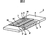
図2は、第1実施形態のRFIDタグの送受信部の構造を示す図である。
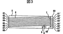
図3は、第1実施形態において磁性コア材に巻き付ける前の平面状のFPCを示す図である。
図4は、第1実施形態のRFIDタグの送受信部の断面構造図である。
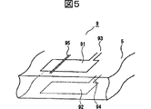
図5は、第1実施形態のRFIDタグのコンデンサ部を表す図である。
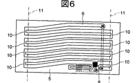
図6は、第1実施形態のRFIDタグの線状導体パターンの接続を表す図である。
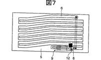
図7は、第1実施形態のRFIDタグにおけるコンデンサの好適な形態を示す図である。
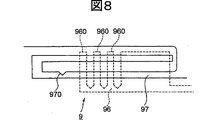
図8は、図7のコンデンサの部分の拡大図である。
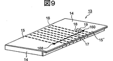
図9は、第2実施形態のRFIDタグの送受信部の構造を表す図である。
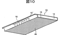
図10は、図9に示す送受信部を下側から見た図である。
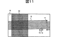
図11は、第2実施形態において磁性コア材に巻き付ける前の平面状のFPCを示す図である。
図12は、第2実施形態のRFIDタグの送受信部の断面構造図である。
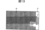
図13は、第2実施形態の第1の変形例において磁性コア材に巻き付ける前の平面状のFPCを示す図である。
図14は、第2実施形態の第1の変形例におけるRFIDタグの送受信部の断面構造図である。
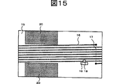
図15は、第2実施形態の第2の変形例において磁性コア材に巻き付ける前の平面状のFPCを示す図である。FIG. 1 is a diagram illustrating an RFID tag according to the first embodiment.
FIG. 2 is a diagram illustrating a structure of a transmission / reception unit of the RFID tag according to the first embodiment.
FIG. 3 is a diagram showing a planar FPC before being wound around the magnetic core material in the first embodiment.
FIG. 4 is a cross-sectional structure diagram of a transmission / reception unit of the RFID tag according to the first embodiment.
FIG. 5 is a diagram illustrating a capacitor unit of the RFID tag according to the first embodiment.
FIG. 6 is a diagram illustrating connection of linear conductor patterns of the RFID tag according to the first embodiment.
FIG. 7 is a diagram illustrating a preferred form of the capacitor in the RFID tag according to the first embodiment.
FIG. 8 is an enlarged view of the capacitor portion of FIG.
FIG. 9 is a diagram illustrating the structure of the transmission / reception unit of the RFID tag according to the second embodiment.
FIG. 10 is a diagram of the transmission / reception unit illustrated in FIG. 9 as viewed from below.
FIG. 11 is a diagram illustrating a planar FPC before being wound around a magnetic core material in the second embodiment.
FIG. 12 is a cross-sectional structure diagram of a transmission / reception unit of the RFID tag according to the second embodiment.
FIG. 13 is a diagram illustrating a planar FPC before being wound around a magnetic core material in the first modification of the second embodiment.
FIG. 14 is a cross-sectional structure diagram of a transmission / reception unit of an RFID tag according to a first modification of the second embodiment.
FIG. 15 is a diagram illustrating a planar FPC before being wound around a magnetic core material in the second modification of the second embodiment.
(第1実施形態)
以下、本発明の第1実施形態について、図1〜図8を参照しつつ説明する。図1は、本発明の第1実施形態に係るRFIDタグを表した図である。図1において、RFIDタグ1は、ABSなどの樹脂ケース2内に送受信部3を組み込みカード状に形成されている。
図2は、第1実施形態に係るRFIDタグ1の送受信部3の構造を示す図である。送受信部3は、図2に示すように、フェライト、フェライト混練樹脂、アモルファスシートなどの磁性コア材4の周囲にFPC5が巻き付けられた構造を備えている。なお、磁性コア材4としては、外力により割れることの無いようフェライト混練樹脂やアモルファスシートなどの可撓性を有する材料を用いることが望ましい。
FPC5は、例えばPET、PI、PEN、液晶ポリマーなどの樹脂を厚さ30μm程度に形成したものである。FPC5上の一方の面には線状導体パターン6及びコンデンサ9が形成され、線状導体パターン6にはFPC5上にエポキシ系接着剤等により接着されたIC8が接続されている。また、FPC5の他方の面には、両端に位置する線状導体パターン6の端部60、69に接続されたクロスオーバーパターン7が形成されている。
ここで、線状導体パターン6やクロスオーパーバターン7は例えば、銅やアルミのエッチングあるいは銀ペーストによる印刷等により形成される。また、コンデンサ9は、図5に示すようにFPC5を介して上面導体91と下面導体92を対向させて形成し接続導体93、94をIC8に接続して形成される。これらの上面導体91、下面導体92、接続導体93、94は上述した線状導体パターン6等と同様にエッチングや印刷等により形成される。
磁性コア材4に巻き付けられたFPC5は、接合部5´で線状導体パターン6の対応部分(61と61´、62と62´など)が半田付け、超音波溶接などで電気的に接続される。こうして磁性コア材4の周囲に導体を配したコイル状アンテナを含む送受信部3を構成することができる。なお、図3は、磁性コア材4に巻き付ける前の平面状のFPC5を示している。
この際には図4に示すように、磁性コア材4にIC収納凹部8´を予め設けておき、FPCの線状導体パターン6及びIC8が設けられた面を内側に巻き込むのが好ましい。この場合には送受信部3は線状導体パターン6、IC8が露出することなく構成され、搬送中の衝撃など外力から保護できる。さらに、FPC5を巻き付ける際の張力は外側の面が強くなるが、破損しやすいIC端子部は比較的張力の低い内側にあるため巻き付け張力により破損することを防止することができる。
また、FPC5は、図6に示すように線状導体パターン6を、隣接する線状導体パターン6と始端同士あるいは終端同士でダミー接続部10により接続しておいてもよい。この場合にはFPC5を巻き付けて線状導体6の一端と他端をクロスオーバーパターン7を介して接続する以前においても、回路が形成されコイル状アンテナとして機能しうるため、RFIDタグ製造工程の初期においてFPC5単体の状態でもIC8の動作確認や導体抵抗、静電容量の確認など各種の動作確認が可能であり、品質の安定した製造を効率的に行うことが可能である。
なお、ダミー接続部10はFPC5を磁性コア材4に巻き付けた後などの適宜の時点に切除線11で切除することにより、結果的には図2に示すような送受信部3を構成することができる。
上述のように得られた送受信部3は、FPC5を磁性コア材4に巻き付ける際や、線状導体パターン6の対応部分(61と61´、62と62´など)が接続される際にその特性にバラツキを生じる場合がある。かかる場合には図5に示すように、例えば、コンデンサ9の上面導体91にレーザー等を使用して切り込み95を入れ、導体の対向面積を減らして容量を減少させることにより特性を補償することができる。この場合に導体をカッターで切断したり、あるいは剥がすことも可能であるが、レーザーを使用する場合はある程度の幅で切り込み95を入れることができ便利である。
次に、コンデンサ9のさらなる好適な形態を図7、8により説明する。
図7は、RFIDタグ1におけるコンデンサ9の好適な形態を示す図であり、図8は、図7に示すコンデンサ9の部分の拡大図である。コンデンサ9はFPC5の一方の面に形成された複数のくし960を有するくし型状導体パターン96と、FPC5の他方の面に形成された例えばミアンダ状の導体パターン97を有している。くし型状導体パターン96と導体パターン97はFPC5を介して互いにその一部が対向するよう配置されている。なお、例えば線状導体パターン6の裏面に形成されるくし型状導体パターン96はFPC5を貫通する接続部12を介してIC8と並列となるよう線状導体パターン6に接続されている。
FPC5のIC8及び線状導体パターン6を内側にして巻き付ける場合には、巻き付け工程前に導体パターン97の一部を切除して粗調整を行うことができる。この際にダミー接続部10を設けておくことにより、粗調整時にもある程度特性を確認しながら行うことが可能である。また、導体パターン97には粗調整用の切除マーク970を設けておき、例えばRFIDタグ1が金属物品上で使用されるか否かにより切除マーク970より先の部分を切除するか否かを選択するなどすると便利である。
次に、FPC5を磁性コア材4に巻き付け、線状導体パターン6の所定の始端、終端を接続し、ダミー接続部10を切除して送受信部3として構成した後、特性を測定しながらFPC5上外側の面に露出しているコンデンサ9のくし状導体パターン96のくし960を一つずつあるいは複数個ずつ切除しながらコンデンサ9の容量ひいては送受信部3の特性の特性を調整することができる。なお、くし状導体パターン96や導体パターン97の切除はパターンをカッターナイフで切断しFPC5から剥がすなどの簡単な作業で行うことができる。
このように形成された送受信部3は樹脂ケースに組み込まれてRFIDタグ1が完成する。
(第2実施形態)
以下、本発明の第2実施形態について、図9〜図15を参照しつつ説明する。第2実施形態においては、RFIDに組み込まれた送受信部の構成が第1実施形態の場合と異なっている。
図9は、第2実施形態に係るRFIDタグ1の送受信部13の構造を示す図である。図9に示す送受信部13は、磁性コア材14の周囲に図2に比べてサイズの大きいFPC15が巻き付けられた構造を備えている。そして、この状態でFPC15には、磁性コア材14に対して内側の面に線状導体パターン16が配置され、外側の面にクロスオーバーパターン17が配置され、線状導体パターン16の端部160、169とクロスオーバーパターン17が接続されている。また、磁性コア材14の角部付近に接合部15´が設けられている。なお、磁性コア材14の材料やFPC15の材料、あるいは各導体パターン形成方法等については、第1実施形態の場合と同様でよい。
一方、図10は、図9に示す送受信部13を下側から見た図である。図10に示すように、磁性コア材14にFPC15を巻き付けた状態で送受信部13の下側には磁性コア材14に対して外側の面に遮蔽導体パターン20が配置されている。この遮蔽導体パターン20は、RFIDタグ1の取り付け対象物である金属物品が接近した際にコイル状アンテナに与える影響を防止するために設けた金属板としての役割を担う。
図9及び図10において、磁性コア材14に巻き付けられたFPC15は、磁性コア材14の角部付近にある接合部15´で、第1実施形態と同様に線状導体パターン16の対応部分が電気的に接続される。なお、接合部15´におけるFPC15の接合には、半田付けや超音波溶接などを用いることができる。
なお、接合部15´が磁性コア材14の角部付近に位置する場合を示したが、これに限らず、遮蔽導体パターン20が配置されない磁性コア材14の上面にて接合してもよい。ただし、磁性コア材14の角部付近でFPC15を接合することにより、RFIDタグ1の製造時にFPC15を磁性コア材14に巻き付けたときに内側に面に配置される線状導体パターン16の接続作業が行いやすくなり、作業性を向上させることができる。
図11は、磁性コア材14に巻き付ける前の平面状のFPC15を示す図であり、一方の面と他方の面の構成を重ねて示している。図11においてFPC15の一方の面には、第1実施形態と同様に、線状導体パターン16及びコンデンサ19が形成され、IC18が接着されて接続される。また、FPC15の他方の面には、第1実施形態と同様のクロスオーバーパターン17に加えて、遮蔽導体パターン20が形成されている。
図11に示すように、FPC15の一方の面に形成された複数の線状導体パターン16は、上述の接合部15´にて電気的に接続したときにコイル状アンテナを構成できる位置関係で構成されている。なお、第1実施形態と同様に線状導体パターン16の始端同士又は終端同士を接続するダミー部を設けてもよい。また、線状導体パターン16の所定箇所には、IC18とコンデンサ19が接続されている。
また、FPC15の他方の面には、図11の右側の領域にクロスオーバーパターン17が形成され、図11の左側の領域に遮蔽導体パターン20が形成されている。この場合、図11の左側の領域にのみ遮蔽導体パターン20が形成されたFPC15を磁性コア材14に巻き付けて接合部15´で接合した場合、図10に示すように、遮蔽導体パターン20を磁性コア材14の下部領域に配置することができる。
後述するように、遮蔽導体パターン20は、図12の形状に限られることなく、多様な形状を持たせて形成することができるが、第2実施形態においては、FPC15において線状導体パターン16が形成された面と異なる面(裏面)に遮蔽導体パターン20を形成する点を特徴としている。上述したように、遮蔽導体パターン20は、外部の取り付け対象物が近接したときにコイル状アンテナが受ける影響を軽減するために設けられるので、コイル状アンテナを構成する線状導体パターン16、クロスオーバーパターン17、IC18、コンデンサ19と遮蔽導体パターン20との間では電気的な接続を持たせないようにする必要がある。
ここで、図12に、図11のFPC15を磁性コア材14に巻き付けた状態の送受信部13の断面構造図を示す。図12においては、中心に磁性コア材14が配置され、その外側にFPC15に形成された線状導体パターン16が配置され、更にその外側にFPC15の樹脂部15aが配置され,また、磁性コア材14の下部領域におけるFPC15に外部には、遮蔽導体パターン20が配置される。この場合、磁性コア材14の周囲には、第1実施形態と同様に線状導体パターン16によって螺旋状の電流流路が形成され、これがコイル状アンテナとして機能する。なお、図12においては、RFIDタグ1の取り付け対象物は、磁性コア材14の下側領域に置かれることを前提とする。
RFIDタグ1を実際に使用する際に上述のような構成されたRFIDタグ1の取り付け対象物である金属物品に取り付けたとき、線状導体パターン16によるコイル状アンテナは、金属物品との間に遮蔽導体パターン20が介在して対向する位置関係が保たれる。よって、金属物品がコイル状アンテナの周波数特性に与える影響を十分に抑えることができる。
一方、線状導体パターン16と遮蔽導体パターン20との間の距離はFPC15の樹脂部15aの厚さにより定まるが、FPC15は、例えば30μm程度の厚さで樹脂部15aが形成されることが一般的である。そして、樹脂部15aは常に一定の厚さを安定に保つことができるので、線状導体パターン16と遮蔽導体パターン20の間隔が変動することに起因する周波数特性の変動を避けることができ、安定な周波数特性を有するコイル状アンテナを構成することができる。
第2実施形態において、FPC15の遮蔽導体パターン20のパターン形状は様々な変更を加えることが可能であり、上述した例に限られず、以下の図13〜図15に示すような様々な変形例がある。図9〜図12に示す例では、FPC15を磁性コア材14に巻き付けたとき、遮蔽導体パターン20が磁性コア材14の下部領域に配置される構成を示したが、第1の変形例は、遮蔽導体パターン20を磁性コア材14の上部領域と下部領域の双方に配置させるような構成を備えている。
第1の変形例における遮蔽導体パターン20の構成を図13及び図14により説明する。図13に示すように、第1の変形例では、FPC15の他方の面に形成される遮蔽導体パターン20の面積を広くしたことが特徴となっている。すなわち、図11の場合は左側の領域にのみ遮蔽導体パターン20が形成されているが、図13の場合は左側と右側を含む領域全体にわたって遮蔽導体パターン20が形成されている。
そして、図14に示すように、図13の遮蔽導体パターン20が形成されたFPC15を磁性コア材14に巻き付けた状態では、磁性コア材14の上部領域と下部領域の双方に遮蔽導体パターン20が配置されることになる。このとき、FPC15の一方の面に形成された線状導体パターン16は、遮蔽導体パターン20によって周囲を取り囲まれる配置になる。
このように、第1の変形例では遮蔽導体パターン20が磁性コア材14と上部及び下部に配置され、金属物品がRFIDタグ1の上下いずれの方向に近接する場合であっても、コイル状アンテナと金属物品の間に遮蔽導体パターン20が介在する位置関係になる。すなわち、第1の変形例によれば、RFIDタグ1の取り付け方向あるいはその反対方向から金属物品が接近する場合であっても、コイル状アンテナの周波数特性に与える影響を軽減できる効果がある。ただし、遮蔽導体パターン20の面積が広くなってコイル状アンテナの間の容量結合が大きくなる結果、RFIDタグ1の共振周波数が下がるので、それを考慮した設計条件を定める必要がある。
次に、第2の変形例における遮蔽導体パターン20の構成を図15により説明する。図15に示すように、第2の変形例では、FPC15の他方の面に形成される遮蔽導体パターン20が、図11の場合と異なった分布をしている。すなわち、図15に示す遮蔽導体パターン20は、線状導体パターン16に対向する領域には遮蔽導体パターン20が形成されず、線状導体パターン16に対向しない周辺部分の領域に遮蔽導体パターン20が形成されている。
上記のように遮蔽導体パターン20を分布させたので、第2の変形例では、FPC15を磁性コア材14に巻き付けたとき、RFIDタグ1の下方に置かれた金属物品とコイル状アンテナが対向する位置関係になり、その側部に遮蔽導体パターン20が配置される状態になる。一方、線状導体パターン16と遮蔽導体パターン20も直接対向しなくなるため、両者の容量結合は小さくなる。従って、外部の金属物品が接近したときのコイル状アンテナの周波数特性に与える影響は、上述の例に比べ若干大きくなるが、ある程度は軽減できるとともに、RFIDタグ1の共振周波数が下がりにくくなる点で大きなメリットがある。
次に、第2実施形態におけるRFIDタグ1の製造工程については、第1実施形態の場合と基本的な流れは共通している。第2実施形態では、FPC15への導体パターンの形成方法と、FPC15の磁性コア材14への巻き付け方法を、図9及び図10の構成に対応させる必要がある。それ以外の点では、線状導体パターン16の切除による粗調整、コンデンサ19の容量の調整などに関して第1実施形態と同様の方法を適用することができる。(First embodiment)
Hereinafter, a first embodiment of the present invention will be described with reference to FIGS. FIG. 1 is a diagram showing an RFID tag according to the first embodiment of the present invention. In FIG. 1, an RFID tag 1 is formed in a card shape by incorporating a transmitting / receiving
FIG. 2 is a diagram illustrating a structure of the transmission /
The
Here, the
The
At this time, as shown in FIG. 4, it is preferable that an
In addition, as shown in FIG. 6, the
In addition, the
The transmitter /
Next, a further preferred form of the
FIG. 7 is a diagram showing a preferred form of the
In the case of winding with the
Next, the
The transmission /
(Second Embodiment)
Hereinafter, a second embodiment of the present invention will be described with reference to FIGS. In 2nd Embodiment, the structure of the transmission / reception part incorporated in RFID differs from the case of 1st Embodiment.
FIG. 9 is a diagram illustrating a structure of the transmission /
On the other hand, FIG. 10 is the figure which looked at the transmission /
9 and 10, the
In addition, although the case where joint part 15 'was located near the corner | angular part of the
FIG. 11 is a view showing the
As shown in FIG. 11, the plurality of
Further, on the other surface of the
As will be described later, the shielding
Here, FIG. 12 shows a cross-sectional structure diagram of the transmission /
When the RFID tag 1 is actually used and attached to a metal article which is an attachment target of the RFID tag 1 configured as described above, the coiled antenna formed by the
On the other hand, the distance between the
In the second embodiment, the pattern shape of the shielding
The configuration of the shielding
As shown in FIG. 14, when the
Thus, in the first modified example, the shielding
Next, the configuration of the shielding
Since the shielding
Next, the basic process for manufacturing the RFID tag 1 in the second embodiment is the same as that in the first embodiment. In the second embodiment, the method for forming the conductor pattern on the
以上の説明で明らかなように、本発明によれば、FPCを利用してRFIDタグにコイル状アンテナを構成したので、効率的に製造可能なRFIDタグを提供するとともに、RFIDタグの効率的な製造方法を提供することができる。
また、FPCに遮蔽導体パターンを形成して周波数特性の変動に対する対策を施したので、コスト増加とサイズの大型化を招くことなく良好な周波数特性を保持し得るRFIDタグを提供することができる。As is clear from the above description, according to the present invention, since the coiled antenna is configured on the RFID tag using FPC, an RFID tag that can be efficiently manufactured is provided, and the RFID tag can be efficiently used. A manufacturing method can be provided.
In addition, since the shield conductor pattern is formed on the FPC to take measures against fluctuations in frequency characteristics, it is possible to provide an RFID tag that can maintain good frequency characteristics without increasing costs and increasing the size.
Claims (23)
磁性コア材と、前記磁性コア材の周囲に巻き付けられたFPCと、前記FPC上に互いに並列して形成された2以上の線状導体パターンと、前記線状導体パターンに接続され前記FPC上に配置されたICと、互いに並列して形成された前記線状導体パターンのうち最も外側に位置する線状導体パターンの一端と他端を電気的に接続するクロスオーバーパターンとを備え、
前記2以上の線状導体パターンは巻き付けられたFPCの接合部で隣接する線状導体パターンをそれらの始端と終端で電気的に接続したことを特徴とするRFIDタグ。An RFID tag comprising a coiled antenna with a conductor disposed around a magnetic core material,
A magnetic core material; an FPC wound around the magnetic core material; two or more linear conductor patterns formed in parallel on the FPC; and the FPC connected to the linear conductor pattern on the FPC An IC that is arranged, and a crossover pattern that electrically connects one end and the other end of the linear conductor pattern located on the outermost side among the linear conductor patterns formed in parallel with each other,
The RFID tag, wherein the two or more linear conductor patterns are electrically connected at the start and end of adjacent linear conductor patterns at the joint portion of the wound FPC.
互いに並列して形成された2以上の線状導体パターンが一面に形成されたFPCを前記磁性コア材に巻き付け、隣接した前記線状導体パターンを電気的に接続することにより、前記磁性コア材の周囲に螺旋状の電流流路を形成し、且つ前記電流流路の一端と他端を電気的に接続することにより、前記コイル状アンテナとしたことを特徴とするRFIDタグ。In an RFID tag including a magnetic core material including at least one magnetic material, a coiled antenna in which a conductor is spirally arranged around the magnetic core material, and an IC,
An FPC having two or more linear conductor patterns formed in parallel with each other is wound around the magnetic core material, and the adjacent linear conductor patterns are electrically connected to each other, thereby An RFID tag characterized in that the coiled antenna is formed by forming a spiral current channel around and electrically connecting one end and the other end of the current channel.
前記接続する工程以前に動作確認を行う工程と、前記接続する工程以前または以降に前記ダミー接続部を切除する工程をさらに有することを特徴とする請求項12乃至14のいずれかに記載のRFIDタグの製造方法。The linear conductor pattern has a dummy connection part connected to the adjacent linear conductor pattern at the start or end, forming a meander-shaped current flow path,
15. The RFID tag according to claim 12, further comprising a step of confirming an operation before the connecting step and a step of cutting the dummy connection portion before or after the connecting step. Manufacturing method.
前記磁性コア材の周囲に前記FPCを巻き付ける工程において、前記FPCの前記線状導体パターンが形成された面が前記磁性コア材に巻き付けられる内側の面となり、前記FPCの遮蔽導体パターンが形成された面が前記磁性コア材に巻き付けられる外側の面となることを特徴とする請求項12乃至14のいずれかに記載のRFIDタグの製造方法。The two or more linear conductor patterns are formed on one surface of the FPC, and a shielding conductor pattern is formed on the other surface of the FPC.
In the step of winding the FPC around the magnetic core material, the surface on which the linear conductor pattern of the FPC is formed becomes the inner surface wound on the magnetic core material, and the shielding conductor pattern of the FPC is formed. The RFID tag manufacturing method according to claim 12, wherein the surface is an outer surface wound around the magnetic core material.
前記磁性コア材の周囲に前記FPCを巻き付ける工程において、少なくともRFIDタグの取り付け対象物に対向する領域に前記遮蔽導体パターンが配置されるように前記FPCを巻き付けることを特徴とする請求項20に記載のRFIDタグ。The interrupting conductor pattern is formed on a part of the surface of the FPC where the interrupting conductor pattern is formed,
The step of winding the FPC around the magnetic core material winds the FPC so that the shielding conductor pattern is disposed at least in a region facing an RFID tag attachment target. RFID tag.
Applications Claiming Priority (5)
| Application Number | Priority Date | Filing Date | Title |
|---|---|---|---|
| JP2002284744 | 2002-09-30 | ||
| JP2002284744 | 2002-09-30 | ||
| JP2003007938 | 2003-01-16 | ||
| JP2003007938 | 2003-01-16 | ||
| PCT/JP2003/012529 WO2004030148A1 (en) | 2002-09-30 | 2003-09-30 | Rfid tag and process for producing the same |
Publications (2)
| Publication Number | Publication Date |
|---|---|
| JPWO2004030148A1 true JPWO2004030148A1 (en) | 2006-01-26 |
| JP4330009B2 JP4330009B2 (en) | 2009-09-09 |
Family
ID=32044651
Family Applications (1)
| Application Number | Title | Priority Date | Filing Date |
|---|---|---|---|
| JP2004539592A Expired - Fee Related JP4330009B2 (en) | 2002-09-30 | 2003-09-30 | RFID tag and manufacturing method thereof |
Country Status (4)
| Country | Link |
|---|---|
| US (1) | US7126482B2 (en) |
| EP (1) | EP1585191A4 (en) |
| JP (1) | JP4330009B2 (en) |
| WO (1) | WO2004030148A1 (en) |
Families Citing this family (59)
| Publication number | Priority date | Publication date | Assignee | Title |
|---|---|---|---|---|
| US8543564B2 (en) | 2002-12-23 | 2013-09-24 | West Publishing Company | Information retrieval systems with database-selection aids |
| US7362285B2 (en) * | 2004-06-21 | 2008-04-22 | Lutron Electronics Co., Ltd. | Compact radio frequency transmitting and receiving antenna and control device employing same |
| US7307527B2 (en) | 2004-07-01 | 2007-12-11 | Avery Dennison Corporation | RFID device preparation system and method |
| US7375631B2 (en) * | 2004-07-26 | 2008-05-20 | Lenovo (Singapore) Pte. Ltd. | Enabling and disabling a wireless RFID portable transponder |
| JP4653440B2 (en) * | 2004-08-13 | 2011-03-16 | 富士通株式会社 | RFID tag and manufacturing method thereof |
| US7242359B2 (en) * | 2004-08-18 | 2007-07-10 | Microsoft Corporation | Parallel loop antennas for a mobile electronic device |
| US7158033B2 (en) | 2004-09-01 | 2007-01-02 | Avery Dennison Corporation | RFID device with combined reactive coupler |
| US7271985B1 (en) * | 2004-09-24 | 2007-09-18 | Storage Technology Corporation | System and method for crosstalk reduction in a flexible trace interconnect array |
| FR2884681B1 (en) * | 2005-04-15 | 2007-06-22 | St Microelectronics Sa | ANTENNA FOR ELECTRONIC LABEL |
| JP4750455B2 (en) | 2005-04-15 | 2011-08-17 | 富士通株式会社 | RFID tag set, RFID tag, and RFID tag component |
| JP2007041666A (en) * | 2005-08-01 | 2007-02-15 | Ricoh Co Ltd | RFID tag and manufacturing method thereof |
| EP1920391B1 (en) | 2005-08-22 | 2016-11-16 | Avery Dennison Retail Information Services, LLC | Method of making rfid devices |
| JP2007060138A (en) * | 2005-08-23 | 2007-03-08 | Nec Tokin Corp | Coil antenna |
| JP4675765B2 (en) * | 2005-12-06 | 2011-04-27 | 株式会社プリモテック | Non-contact IC card |
| US7705733B2 (en) * | 2006-01-06 | 2010-04-27 | Warsaw Orthopedic, Inc. | Coiled RFID tag |
| US20070159337A1 (en) * | 2006-01-12 | 2007-07-12 | Sdgi Holdings, Inc. | Modular RFID tag |
| JP5034371B2 (en) | 2006-02-10 | 2012-09-26 | 富士通株式会社 | RFID tag manufacturing method and RFID tag |
| JP5344267B2 (en) * | 2006-02-10 | 2013-11-20 | 富士通株式会社 | RFID tag manufacturing method and RFID tag |
| JP3933191B1 (en) * | 2006-03-13 | 2007-06-20 | 株式会社村田製作所 | Portable electronic devices |
| DE102006017992A1 (en) * | 2006-04-07 | 2007-10-18 | Balluff Gmbh | Data carrier / transmitting device and method for producing a data carrier / transmitting device |
| EP1860458A1 (en) * | 2006-05-22 | 2007-11-28 | Interuniversitair Microelektronica Centrum | Detection of resonant tags by UWB radar |
| DE102006029250A1 (en) * | 2006-06-26 | 2007-12-27 | Giesecke & Devrient Gmbh | Method for producing a transponder |
| JP3957000B1 (en) | 2006-07-07 | 2007-08-08 | 株式会社村田製作所 | Antenna coil for board mounting and antenna device |
| JP4956152B2 (en) | 2006-11-21 | 2012-06-20 | 株式会社スマート | Sensor tag multifaceted image system |
| FR2909258B1 (en) * | 2006-11-30 | 2012-08-03 | Prosonic | MINIATURE TRANSPONDER AND IDENTIFICATION SYSTEM COMPRISING SUCH A TRANSPONDER AND AN ADAPTIVE READER. |
| US7681301B2 (en) * | 2007-03-07 | 2010-03-23 | James Neil Rodgers | RFID silicon antenna |
| EP2341463A3 (en) * | 2007-04-19 | 2014-06-11 | BALLUFF GmbH | Data carrier/transmission device and method for manufacturing it |
| US8062445B2 (en) * | 2007-08-06 | 2011-11-22 | Avery Dennison Corporation | Method of making RFID devices |
| JP5260031B2 (en) * | 2007-11-20 | 2013-08-14 | 株式会社スマート | Wireless transmission / reception device, non-contact information recording medium, information reading / writing device, and management system |
| US7847697B2 (en) | 2008-02-14 | 2010-12-07 | 3M Innovative Properties Company | Radio frequency identification (RFID) tag including a three-dimensional loop antenna |
| GB0906644D0 (en) | 2009-04-17 | 2009-06-03 | Imec Inter Uni Micro Electr | Magnetic resonance imaging of single domain nano-particles |
| EP2331982B1 (en) | 2008-09-30 | 2018-11-14 | IMEC vzw | Pulsed epr detection |
| KR101035054B1 (en) * | 2008-12-24 | 2011-05-19 | 전자부품연구원 | Tag Antenna and its manufacturing method |
| EP2416446A4 (en) * | 2009-03-31 | 2013-03-13 | Toda Kogyo Corp | Composite rf tag and tool provided with the composite rf tag |
| US9136600B2 (en) | 2010-09-30 | 2015-09-15 | Murata Manufacturing Co., Ltd. | Antenna |
| JP5526726B2 (en) * | 2009-11-20 | 2014-06-18 | 富士通株式会社 | Wireless tag |
| US9160070B2 (en) * | 2010-02-16 | 2015-10-13 | William N. Carr | Radiation-hardened RFID tags |
| US9112263B2 (en) * | 2010-02-25 | 2015-08-18 | Stmicroelectronics S.R.L. | Electronic communications device with antenna and electromagnetic shield |
| JP2011238016A (en) * | 2010-05-10 | 2011-11-24 | Sony Corp | Non-contact communication medium, antenna pattern arrangement medium, communication device and antenna adjustment method |
| CN104704585B (en) | 2012-08-15 | 2019-01-04 | 诺基亚技术有限公司 | Apparatus and method for power harvesting and/or wireless communication |
| TWI478070B (en) | 2012-08-29 | 2015-03-21 | E Ink Holdings Inc | Controlling method for coexistence of radio frequency identification and display |
| JP6079248B2 (en) * | 2013-01-15 | 2017-02-15 | オムロン株式会社 | RF tag, manufacturing method thereof, and primary molded body for RF tag |
| JP2014183428A (en) * | 2013-03-19 | 2014-09-29 | Dexerials Corp | Coil module, antenna device and electronic device |
| WO2014199136A1 (en) * | 2013-06-12 | 2014-12-18 | Tyco Electronics Uk Ltd. | Flexible rfid tag assembly |
| AT514661A1 (en) * | 2013-07-25 | 2015-02-15 | Seibersdorf Labor Gmbh | container |
| TWI538294B (en) * | 2013-08-14 | 2016-06-11 | 華碩電腦股份有限公司 | Antenna device |
| CN103647143B (en) * | 2013-11-25 | 2015-11-18 | 深圳市新国都技术股份有限公司 | A kind of tubbiness antenna for POS and preparation method thereof |
| CN105811083B (en) * | 2014-12-30 | 2020-09-01 | 上海伯乐电子有限公司 | Flexible RFID antenna and POS machine device and electronic equipment applying same |
| JP6274135B2 (en) * | 2015-03-12 | 2018-02-07 | 株式会社村田製作所 | Coil module |
| CN106503779A (en) * | 2015-09-08 | 2017-03-15 | 凸版印刷株式会社 | Band IC tag paster |
| CN106022436A (en) * | 2016-05-12 | 2016-10-12 | 安徽晶太信息科技有限公司 | Butterfly transponder and production method thereof |
| SK289113B6 (en) * | 2016-09-19 | 2023-09-13 | Logomotion, S.R.O | Antenna with core, especially miniature RFID and/or NFC antenna and its mode of production |
| JP2018201165A (en) | 2017-05-29 | 2018-12-20 | 株式会社リコー | Antenna device and method for manufacturing the same |
| US11276286B2 (en) * | 2017-06-22 | 2022-03-15 | Checkpoint Systems, Inc. | Detectable folded coil |
| US11544518B2 (en) | 2017-06-22 | 2023-01-03 | Checkpoint Systems, Inc. | Deactivatable metal tag |
| WO2019146237A1 (en) * | 2018-01-23 | 2019-08-01 | 株式会社村田製作所 | Rfid tag, article provided with rfid tag, and method for manufacturing article |
| TWM573545U (en) | 2018-09-18 | 2019-01-21 | 振鋒企業股份有限公司 | Near field communication data carrier mounted on metal object |
| CN120197636A (en) * | 2018-11-15 | 2025-06-24 | 艾利丹尼森零售信息服务有限公司 | Recyclable radio frequency identification transponder part and method for producing the same |
| IT202000024067A1 (en) * | 2020-10-13 | 2022-04-13 | Easting Electronics Societa’ A Responsabilita’ Limitata | SUPPLY DEVICE FOR MEASURING EQUIPMENT OF PHYSICAL PARAMETERS OF MOVING MECHANICAL PARTS |
Family Cites Families (11)
| Publication number | Priority date | Publication date | Assignee | Title |
|---|---|---|---|---|
| EP0554486B1 (en) * | 1992-02-05 | 1998-07-22 | Texas Instruments Deutschland Gmbh | Method of producing a flexible HF antenna |
| GB9220409D0 (en) * | 1992-09-28 | 1992-11-11 | Texas Instruments Holland | Shielded transponder |
| JPH0837351A (en) * | 1994-07-21 | 1996-02-06 | Amp Japan Ltd | Flexible circuit board harness device and flexible circuit board used therefor |
| US6098271A (en) * | 1994-10-04 | 2000-08-08 | Fujitsu Limited | Method for assembling a magnetic disk drive with a relaying flexible printed circuit sheet |
| JPH08204432A (en) * | 1995-01-27 | 1996-08-09 | Citizen Watch Co Ltd | Antenna structure for portable electronic equipment |
| US6130612A (en) * | 1997-01-05 | 2000-10-10 | Intermec Ip Corp. | Antenna for RF tag with a magnetoelastic resonant core |
| JPH11328354A (en) * | 1998-05-20 | 1999-11-30 | Toppan Printing Co Ltd | Resin card and method of manufacturing the same |
| JP4117443B2 (en) * | 2000-12-21 | 2008-07-16 | 三菱マテリアル株式会社 | Method of manufacturing antenna coil for RFID |
| JP4565595B2 (en) * | 2001-02-16 | 2010-10-20 | トッパン・フォームズ株式会社 | Non-contact type antenna for data transceiver and its capacitance adjustment method |
| JP4168597B2 (en) * | 2001-03-13 | 2008-10-22 | 三菱マテリアル株式会社 | Transponder antenna |
| US6549176B2 (en) * | 2001-08-15 | 2003-04-15 | Moore North America, Inc. | RFID tag having integral electrical bridge and method of assembling the same |
-
2003
- 2003-09-30 WO PCT/JP2003/012529 patent/WO2004030148A1/en not_active Ceased
- 2003-09-30 EP EP03798564A patent/EP1585191A4/en not_active Withdrawn
- 2003-09-30 JP JP2004539592A patent/JP4330009B2/en not_active Expired - Fee Related
-
2005
- 2005-03-30 US US11/092,906 patent/US7126482B2/en not_active Expired - Fee Related
Also Published As
| Publication number | Publication date |
|---|---|
| WO2004030148A1 (en) | 2004-04-08 |
| US7126482B2 (en) | 2006-10-24 |
| EP1585191A4 (en) | 2007-03-14 |
| US20050179552A1 (en) | 2005-08-18 |
| EP1585191A1 (en) | 2005-10-12 |
| JP4330009B2 (en) | 2009-09-09 |
Similar Documents
| Publication | Publication Date | Title |
|---|---|---|
| JP4330009B2 (en) | RFID tag and manufacturing method thereof | |
| CN101213567B (en) | Antenna coil and antenna device for substrate mounting | |
| JP4893631B2 (en) | Antenna device | |
| KR100960210B1 (en) | RDF tag and its manufacturing method | |
| KR101850806B1 (en) | Antenna | |
| US8031127B2 (en) | Semiconductor memory module incorporating antenna | |
| CN101233533B (en) | Storage medium with built-in antenna | |
| CN101346852B (en) | Wireless IC device | |
| JP5099846B2 (en) | Electromagnetic induction module | |
| KR100970072B1 (en) | Tag antenna, and tag | |
| JP5260031B2 (en) | Wireless transmission / reception device, non-contact information recording medium, information reading / writing device, and management system | |
| EP2413424B1 (en) | Antenna device and communication apparatus including the same | |
| WO2014038209A1 (en) | Antenna device and communications device | |
| CN103620868A (en) | Antenna device and communication terminal device | |
| CN101366148A (en) | RFID tag, method for manufacturing RFID tag, and method for installing RFID tag | |
| CN101208827A (en) | radio frequency identification tag | |
| JP5199259B2 (en) | Tag antenna for tag and RFID tag using the same | |
| JP2019004266A (en) | Antenna device and electronic apparatus | |
| JP2006164083A (en) | Non-contact communication antenna module and portable information terminal having the same | |
| JP4608258B2 (en) | Smart label and manufacturing method thereof | |
| JP2006262054A (en) | Antenna module and portable information terminal having the same | |
| CN105531722A (en) | Non-contact ic label | |
| JP4775292B2 (en) | Wireless IC device and manufacturing method thereof | |
| CN120237429A (en) | Antenna device and IC card having the same | |
| JP2008040862A (en) | Rfid reader/writer |
Legal Events
| Date | Code | Title | Description |
|---|---|---|---|
| A621 | Written request for application examination |
Free format text: JAPANESE INTERMEDIATE CODE: A621 Effective date: 20060901 |
|
| RD03 | Notification of appointment of power of attorney |
Free format text: JAPANESE INTERMEDIATE CODE: A7423 Effective date: 20081027 |
|
| A131 | Notification of reasons for refusal |
Free format text: JAPANESE INTERMEDIATE CODE: A131 Effective date: 20081028 |
|
| A02 | Decision of refusal |
Free format text: JAPANESE INTERMEDIATE CODE: A02 Effective date: 20090303 |
|
| RD05 | Notification of revocation of power of attorney |
Free format text: JAPANESE INTERMEDIATE CODE: A7425 Effective date: 20090401 |
|
| A521 | Request for written amendment filed |
Free format text: JAPANESE INTERMEDIATE CODE: A523 Effective date: 20090429 |
|
| A911 | Transfer to examiner for re-examination before appeal (zenchi) |
Free format text: JAPANESE INTERMEDIATE CODE: A911 Effective date: 20090520 |
|
| TRDD | Decision of grant or rejection written | ||
| A01 | Written decision to grant a patent or to grant a registration (utility model) |
Free format text: JAPANESE INTERMEDIATE CODE: A01 Effective date: 20090609 |
|
| A01 | Written decision to grant a patent or to grant a registration (utility model) |
Free format text: JAPANESE INTERMEDIATE CODE: A01 |
|
| A61 | First payment of annual fees (during grant procedure) |
Free format text: JAPANESE INTERMEDIATE CODE: A61 Effective date: 20090611 |
|
| FPAY | Renewal fee payment (event date is renewal date of database) |
Free format text: PAYMENT UNTIL: 20120626 Year of fee payment: 3 |
|
| FPAY | Renewal fee payment (event date is renewal date of database) |
Free format text: PAYMENT UNTIL: 20120626 Year of fee payment: 3 |
|
| FPAY | Renewal fee payment (event date is renewal date of database) |
Free format text: PAYMENT UNTIL: 20130626 Year of fee payment: 4 |
|
| LAPS | Cancellation because of no payment of annual fees |