JPWO2003079429A1 - Manufacturing method of semiconductor integrated circuit device - Google Patents
Manufacturing method of semiconductor integrated circuit device Download PDFInfo
- Publication number
- JPWO2003079429A1 JPWO2003079429A1 JP2003577326A JP2003577326A JPWO2003079429A1 JP WO2003079429 A1 JPWO2003079429 A1 JP WO2003079429A1 JP 2003577326 A JP2003577326 A JP 2003577326A JP 2003577326 A JP2003577326 A JP 2003577326A JP WO2003079429 A1 JPWO2003079429 A1 JP WO2003079429A1
- Authority
- JP
- Japan
- Prior art keywords
- insulating film
- integrated circuit
- wiring
- manufacturing
- circuit device
- Prior art date
- Legal status (The legal status is an assumption and is not a legal conclusion. Google has not performed a legal analysis and makes no representation as to the accuracy of the status listed.)
- Pending
Links
Images


Classifications
-
- H—ELECTRICITY
- H10—SEMICONDUCTOR DEVICES; ELECTRIC SOLID-STATE DEVICES NOT OTHERWISE PROVIDED FOR
- H10W—GENERIC PACKAGES, INTERCONNECTIONS, CONNECTORS OR OTHER CONSTRUCTIONAL DETAILS OF DEVICES COVERED BY CLASS H10
- H10W20/00—Interconnections in chips, wafers or substrates
- H10W20/01—Manufacture or treatment
- H10W20/071—Manufacture or treatment of dielectric parts thereof
- H10W20/074—Manufacture or treatment of dielectric parts thereof of dielectric parts comprising thin functional dielectric layers, e.g. dielectric etch-stop, barrier, capping or liner layers
- H10W20/077—Manufacture or treatment of dielectric parts thereof of dielectric parts comprising thin functional dielectric layers, e.g. dielectric etch-stop, barrier, capping or liner layers on sidewalls or on top surfaces of conductors
-
- H—ELECTRICITY
- H10—SEMICONDUCTOR DEVICES; ELECTRIC SOLID-STATE DEVICES NOT OTHERWISE PROVIDED FOR
- H10P—GENERIC PROCESSES OR APPARATUS FOR THE MANUFACTURE OR TREATMENT OF DEVICES COVERED BY CLASS H10
- H10P52/00—Grinding, lapping or polishing of wafers, substrates or parts of devices
- H10P52/40—Chemomechanical polishing [CMP]
- H10P52/403—Chemomechanical polishing [CMP] of conductive or resistive materials
-
- H—ELECTRICITY
- H10—SEMICONDUCTOR DEVICES; ELECTRIC SOLID-STATE DEVICES NOT OTHERWISE PROVIDED FOR
- H10P—GENERIC PROCESSES OR APPARATUS FOR THE MANUFACTURE OR TREATMENT OF DEVICES COVERED BY CLASS H10
- H10P70/00—Cleaning of wafers, substrates or parts of devices
- H10P70/20—Cleaning during device manufacture
- H10P70/27—Cleaning during device manufacture during, before or after processing of conductive materials, e.g. polysilicon or amorphous silicon layers
- H10P70/277—Cleaning during device manufacture during, before or after processing of conductive materials, e.g. polysilicon or amorphous silicon layers the processing being a planarisation of conductive layers
-
- H—ELECTRICITY
- H10—SEMICONDUCTOR DEVICES; ELECTRIC SOLID-STATE DEVICES NOT OTHERWISE PROVIDED FOR
- H10W—GENERIC PACKAGES, INTERCONNECTIONS, CONNECTORS OR OTHER CONSTRUCTIONAL DETAILS OF DEVICES COVERED BY CLASS H10
- H10W20/00—Interconnections in chips, wafers or substrates
- H10W20/40—Interconnections external to wafers or substrates, e.g. back-end-of-line [BEOL] metallisations or vias connecting to gate electrodes
- H10W20/41—Interconnections external to wafers or substrates, e.g. back-end-of-line [BEOL] metallisations or vias connecting to gate electrodes characterised by their conductive parts
- H10W20/44—Conductive materials thereof
- H10W20/4403—Conductive materials thereof based on metals, e.g. alloys, metal silicides
- H10W20/4421—Conductive materials thereof based on metals, e.g. alloys, metal silicides the principal metal being copper
-
- H—ELECTRICITY
- H10—SEMICONDUCTOR DEVICES; ELECTRIC SOLID-STATE DEVICES NOT OTHERWISE PROVIDED FOR
- H10W—GENERIC PACKAGES, INTERCONNECTIONS, CONNECTORS OR OTHER CONSTRUCTIONAL DETAILS OF DEVICES COVERED BY CLASS H10
- H10W20/00—Interconnections in chips, wafers or substrates
- H10W20/40—Interconnections external to wafers or substrates, e.g. back-end-of-line [BEOL] metallisations or vias connecting to gate electrodes
- H10W20/45—Interconnections external to wafers or substrates, e.g. back-end-of-line [BEOL] metallisations or vias connecting to gate electrodes characterised by their insulating parts
- H10W20/47—Interconnections external to wafers or substrates, e.g. back-end-of-line [BEOL] metallisations or vias connecting to gate electrodes characterised by their insulating parts comprising two or more dielectric layers having different properties, e.g. different dielectric constants
Landscapes
- Internal Circuitry In Semiconductor Integrated Circuit Devices (AREA)
Abstract
化学的機械研磨法を用いて絶縁膜の開口部内にCu配線を形成した後、Cu配線の表面をキャップ絶縁膜で覆うプロセスを含むLSIの製造ラインにおいて、Cu配線の形成からキャップ絶縁膜の堆積までを4日以内に実施する。また、後洗浄処理工程からキャップ絶縁膜の堆積工程までの期間が4日を経過した半導体基板に対して再生処理を施すことにより、TDDB寿命の劣化を最小限に止め、LSIの信頼性、製造歩留まりを確保する。In the LSI manufacturing line including the process of forming the Cu wiring in the opening of the insulating film using the chemical mechanical polishing method and then covering the surface of the Cu wiring with the cap insulating film, the deposition of the cap insulating film from the formation of the Cu wiring. To within 4 days. In addition, by performing reprocessing on a semiconductor substrate that has passed 4 days from the post-cleaning process to the cap insulating film deposition process, the degradation of the TDDB life is minimized, and the reliability and manufacturing of the LSI Ensure yield.
Description
技術分野
本発明は、半導体集積回路装置の製造技術に関し、特に、化学的機械研磨(Chemical Mechanical Polishing)法を用いて銅(Cu)を主成分とする導電膜からなる埋込み配線を形成する工程を有する半導体集積回路装置の製造に適用して有効な技術に関するものである。
背景技術
半導体基板上の埋込み配線構造は、絶縁膜に形成された配線溝や孔などの配線埋込み用開口部内に配線用金属膜を埋め込んだ後、開口部の外側の不要な金属膜を化学的機械研磨法で除去するシングルダマシン(Single−Damascene)あるいはデュアルダマシン(Dual−Damascene)と呼ばれるダマシン配線技術によって形成されている。
しかし、金属膜が銅(Cu)である場合は、アルミニウム(Al)のような他の配線用金属膜と比較して絶縁膜中に拡散され易いことから、Cu配線が絶縁膜と直接接しないように、Cu配線の底面および側面を薄いバリアメタル膜で覆うと共に、Cu配線の表面をキャップ絶縁膜で被覆することによって、Cu配線中のCu原子が周囲の絶縁膜に拡散するのを防いでいる。
Cu配線中のCu原子が周囲の絶縁膜に拡散するのを防ぐ技術については、特開平11−111843号公報や特開平10−50632号公報などに記載がある。このうち、特開平11−111843号公報は、Cu配線の上面を絶縁膜の上面よりも低く形成し、そこにバリア絶縁膜を埋め込む構造を開示している。また、特開平10−50632号公報は、Cu配線とバリアメタル膜のそれぞれの上面を絶縁膜の上面よりも低く形成し、そこにバリア絶縁膜を埋め込む構造を開示している。
発明の開示
本発明者が開発中のLSIは、概略次のようなプロセスによってCu配線を形成している。
まず、半導体基板(ウエハ)上に堆積した絶縁膜に開口部を形成した後、この開口部の内部を含む絶縁膜上に窒化チタン膜などからなるバリアメタル膜を薄く堆積し、続いてバリアメタルの上部に開口部の深さよりも厚い膜厚を有するCu膜を堆積する。次に、開口部の外側の不要なCu膜とバリアメタル膜を化学的機械研磨法で除去することにより、開口部の内部にCu配線を形成する。
次に、Cu配線が形成された半導体基板を洗浄処理部に搬送し、上記研磨処理工程で半導体基板の表面に付着したスラリなどの異物を除去するための洗浄(以下、後洗浄という)を行う。
この後洗浄処理工程は、アルカリ洗浄処理とその後の酸洗浄処理とからなる。アルカリ洗浄処理は、半導体基板の表面に付着した酸化剤を含む酸性のスラリの中和を目的とするもので、弱アルカリ薬液を供給しながら半導体基板の表面を洗浄する。また、酸洗浄処理は、残留金属の除去、絶縁膜の表面のダングリングボンドの低減および絶縁膜の表面の凹凸の除去などを目的とするもので、酸を含む薬液を供給しながら半導体基板の表面を洗浄する。
なお、上記薬液に含まれる酸が希フッ酸(DHF)のような強酸である場合は、化学的機械研磨処理で発生したCu配線の表面の薄い酸化層(CuO)が除去されるだけでなく、Cu配線それ自体もエッチングされてしまうので、Cu配線の断面積が小さくなり、電気抵抗が大きくなる虞れがある。従って、特にCu配線の線幅が微細である場合は、有機酸のような弱酸を含む薬液を使用することが望ましい。ただし、有機酸を含む薬液で洗浄を行った場合は、Cu配線の表面の酸化層(CuO)が除去されないので、洗浄後に水素アニールなどの還元処理を行って酸化層(CuO)を除去する必要がある。
次に、上記後洗浄処理が終了した半導体基板の表面にプラズマCVD法などを用いて窒化シリコン膜などからなるキャップ絶縁膜を堆積する。
ここで、本発明者は、上記後洗浄処理が終了してからキャップ絶縁膜を堆積するまでの間に、半導体基板(ウエハ)をクリーンルーム内に放置しておいた場合、一定時間経過後にCu配線のTDDB(Time Dependence on Dielectric Breakdown)寿命が急激に低下するという現象を見出した。このTDDB寿命とは、絶縁破壊の時間的依存性を客観的に計る尺度であって、所定の温度(例えば140℃)の測定条件下でCu配線間に比較的高い電圧を加え、電圧印加から絶縁破壊までの時間を印加電界に対してプロットしたグラフを作成し、このグラフから実際の使用電界強度(例えば0.2MV/cm)に外挿して求めた時間(寿命)をいう。
従って、半導体基板上にCu配線を形成する場合は、研磨後の後洗浄処理からキャップ絶縁膜を堆積するまでの間にCu配線のTDDB寿命が低下するのを防ぐ何らかの対策が必要となる。
本発明の目的は、Cu配線のTDDB寿命の低下を抑制することのできる技術を提供することにある。
本発明の前記ならびにその他の目的と新規な特徴は、本明細書の記述および添付図面から明らかになるであろう。
本願において開示される発明のうち、代表的なものの概要を簡単に説明すれば、以下の通りである。
本願の一発明による半導体集積回路装置の製造方法は、(a)半導体基板上に第1絶縁膜を堆積した後、前記第1絶縁膜に配線埋込み用の開口部を形成する工程と、(b)前記開口部内を含む前記第1絶縁膜上にCuを主成分として含む導電膜を堆積する工程と、(c)前記導電膜を化学的および機械的に研磨して前記開口部内に残すことにより、前記開口部内にCu配線を形成する工程と、(d)前記(c)工程の後、前記半導体基板の表面を洗浄する工程と、(e)前記(d)工程の後、前記半導体基板上に第2絶縁膜を堆積することによって、前記Cu配線の表面を前記第2絶縁膜で被覆する工程とを含み、前記(d)工程が終了した後、4日以内に前記(e)工程を実施するように製造ラインの管理を行うものである。
発明を実施するための最良の形態
以下、本発明の実施の形態を図面に基づいて詳細に説明する。なお、実施の形態を説明するための全図において同一機能を有するものは同一の符号を付し、その繰り返しの説明は省略する。
本実施の形態は、半導体基板に形成した相補型MISFET(Complementary Metal Insulator Semiconductor Field Effect Transistor)の上部にCu配線を形成するLSIの製造方法に適用したものである。このLSIの製造方法を図面に従って説明すれば、次の通りである。
まず、図1に示すように、単結晶シリコンからなるウエハ状の半導体基板(以下、基板というが、ウエハということもある)1を用意し、この基板1の主面に素子分離溝2、p型ウエル4およびn型ウエル5を形成した後、p型ウエル4にnチャネル型MISFETQnを形成し、n型ウエル5にpチャネル型MISFETQpを形成する。
上記素子分離溝2を形成するには、素子分離領域の基板1をエッチングして溝を形成した後、溝の内部を含む基板1上にCVD法で酸化シリコン膜3を堆積し、続いて溝の外部の酸化シリコン膜3を化学的機械研磨法によって除去する。また、p型ウエル4およびn型ウエル5を形成するには、基板1の一部にホウ素をイオン注入し、他の一部にリンをイオン注入した後、基板1を熱処理することによって、これらの不純物を基板1内に拡散させる。
nチャネル型MISFETQnおよびpチャネル型MISFETQpは、周知のプロセスのいずれを用いて形成してもよいが、例えば次のように形成する。まず、基板1をスチーム酸化することによって、p型ウエル4およびn型ウエル5のそれぞれの表面に酸化シリコン膜からなるゲート絶縁膜6を形成した後、ゲート絶縁膜6の上部にCVD法で多結晶シリコン膜を堆積し、続いてp型ウエル4の上部の多結晶シリコン膜にリンをイオン注入し、n型ウエル5の上部の多結晶シリコン膜にホウ素をイオン注入した後、フォトレジスト膜をマスクにしたドライエッチングで多結晶シリコン膜をパターニングすることにより、ゲート電極7を形成する。
次に、p型ウエル4にリンまたはヒ素をイオン注入することによって低不純物濃度のn−型半導体領域8を形成し、n型ウエル5にホウ素をイオン注入することによって低不純物濃度のp−型半導体領域9を形成した後、基板1上にCVD法で窒化シリコン膜を堆積し、続いてこの窒化シリコン膜を異方的にエッチングすることによって、ゲート電極7の側壁にサイドウォールスペーサ10を形成する。次に、p型ウエル4にリンまたはヒ素をイオン注入することによって高不純物濃度のn+型半導体領域11(ソース、ドレイン)を形成し、n型ウエル5にホウ素をイオン注入することによって高不純物濃度のp+型半導体領域12(ソース、ドレイン)を形成する。
次に、基板1の表面を洗浄した後、ゲート電極7、n+型半導体領域11(ソース、ドレイン)およびp+型半導体領域12(ソース、ドレイン)のそれぞれの表面にシリサイド層13を形成する。シリサイド層13を形成するには、基板1上にスパッタリング法でCo(コバルト)膜を堆積し、次いで窒素ガス雰囲気中で熱処理を行って基板1およびゲート電極7とCo膜とを反応させた後、未反応のCo膜をウェットエッチングで除去する。ここまでの工程で、nチャネル型MISFETQnおよびpチャネル型MISFETQpが完成する。
次に、図2に示すように、nチャネル型MISFETQnおよびpチャネル型MISFETQpの上部に第1層目のW(タングステン)配線20を形成する。
W配線20を形成するには、まず基板1上にCVD法で窒化シリコン膜15および酸化シリコン膜16を堆積し、続いてn+型半導体領域11(ソース、ドレイン)およびp+型半導体領域12(ソース、ドレイン)のそれぞれの上部の酸化シリコン膜16および窒化シリコン膜15をドライエッチングしてコンタクトホール17を形成した後、コンタクトホール17の内部にメタルプラグ18を形成する。
上記酸化シリコン膜16は、モノシラン(SiH4)をソースガスに用いた通常のCVD法で形成される酸化シリコン膜の他、BPSG(Boron−doped Phospho Silicate Glass)膜、あるいはスピン塗布法によって形成されるSOG(Spin On Glass)膜などで構成してもよい。
メタルプラグ18を形成するには、コンタクトホール17の内部を含む酸化シリコン膜16上にCVD法でTiN(窒化チタン)膜とW膜とを堆積し、続いて酸化シリコン膜16の上部の不要なTiN膜およびW膜を化学的機械研磨法によって除去する。
次に、酸化シリコン膜16の上部にスパッタリング法でW膜を堆積し、フォトレジスト膜をマスクにしたドライエッチングでこのW膜をパターニングすることにより、酸化シリコン膜16の上部に第1層目のW配線20を形成する。第1層目のW配線20は、コンタクトホール17の内部に埋め込まれたメタルプラグ18を介してnチャネル型MISFETQnのソース、ドレイン(n+型半導体領域11)またはpチャネル型MISFETQpのソース、ドレイン(p+型半導体領域12)と電気的に接続される。
次に、図3に示すように、W配線20の上部にCVD法または塗布法で2層の絶縁膜21、22を堆積し、続いてフォトレジスト膜をマスクにしたドライエッチングで絶縁膜21、22にスルーホール23を形成した後、スルーホール23の内部にメタルプラグ24を形成する。
ここで、下層の絶縁膜21は、W配線20同士の寄生容量あるいはW配線20と次の工程で形成される第2層目の配線との寄生容量を低減するために、酸化シリコンよりも誘電率が低い有機ポリマー、有機シリカガラスなどの絶縁材料で構成する。この種の有機ポリマーとしては、例えばSiLK(米The Dow Chemical Co製、比誘電率=2.7、耐熱温度=490℃以上、絶縁破壊耐圧=4.0〜5.0MV/Vm)またはポリアリルエーテル(PAE)系材料のFLARE(米Honeywell Electronic Materials製、比誘電率=2.8、耐熱温度=400℃以上)などがある。また、有機シリカガラスとしては、例えばHSG−R7(日立化成工業製、比誘電率=2.8、耐熱温度=650℃)、Black Diamond(米Applied Materials,Inc製、比誘電率=3.0〜2.4、耐熱温度=450℃)、p−MTES(日立開発製、比誘電率=3.2)、CORAL(米Novellus Systems,Inc製、比誘電率=2.7〜2.4、耐熱温度=500℃)、Aurora2.7(日本エー・エス・エム社製、比誘電率=2.7、耐熱温度=450℃)などのSiOC系材料がある。絶縁膜21は、上記した有機系絶縁材料の他、SiOF系材料、HSQ(hydrogen silsesquioxane)系材料、MSQ(methyl silsesquioxane)系材料、ポーラスHSQ系材料、ポーラスMSQ材料などで構成してもよい。
絶縁膜21の上部の絶縁膜22は、無機系絶縁材料に比べて機械的強度や耐湿性が低い絶縁膜21を保護するために形成する。絶縁膜22は、例えばCVD法で堆積した酸化シリコン膜の他、酸化シリコン膜よりも誘電率が低い炭化シリコン(SiC)膜または炭窒化シリコン(SiCN)膜などで構成する。炭化シリコン膜や炭窒化シリコン(SiCN)膜としては、例えばBLOk(AMAT社製)がある。
絶縁膜21、22に形成したスルーホール23の内部にメタルプラグ24を形成するには、絶縁膜22上にスパッタリング法でW膜を堆積した後、酸化シリコン膜22の上部の不要なW膜を化学的機械研磨法によって除去する。
次に、図4に示すように、酸化シリコン膜22の上部にCVD法で2層の絶縁膜25、26を堆積した後、フォトレジスト膜をマスクにしたドライエッチングでスルーホール23の上部の絶縁膜25、26に配線溝27を形成する。
上記2層の絶縁膜25、26のうち、上層の絶縁膜26は、例えば酸素とテトラエトキシシラン(TEOS)をソースガスに用いて堆積される酸化シリコン膜で構成する。下層の絶縁膜25は、絶縁膜26をエッチングして配線溝27を形成する際、酸化シリコン膜などからなる下層の絶縁膜22がエッチングされるのを防ぐストッパ膜となるもので、例えば窒化シリコン膜のように酸化シリコン膜に対するエッチング選択比が大きい絶縁膜で構成する。また、配線間寄生容量を低減する観点から、窒化シリコン膜よりも誘電率が低い酸窒化シリコン(SiON)膜や炭窒化シリコン(SiCN)膜などで構成してもよい。
次に、図5に示すように、配線溝27の内部を含む絶縁膜26の上部に窒化チタン膜などからなるバリアメタル膜28をスパッタリング法で堆積した後、バリアメタル膜28の上部に配線溝27の深さよりも厚い膜厚を有するCu膜30aをスパッタリング法で堆積する。
バリアメタル膜28は、配線溝27の内部に堆積したCu膜30aが周囲の絶縁膜26中に拡散したり、Cu膜30aと絶縁膜26の接着性を向上させたりするために形成する。バリアメタル膜28は、窒化チタン膜の他、窒化タングステン(WN)膜、窒化タンタル(TaN)膜、チタンタングステン(TiW)膜などの導電膜で構成することもできる。
Cu膜30aをスパッタリング法で形成する場合は、成膜後に基板1を非酸化性雰囲気(例えば水素雰囲気)中で熱処理してCu膜30aをリフローさせる。また、スパッタリング法としては、Cu膜30aを配線溝27の内部に良好に埋め込むことのできるロングスロースパッタリング法やコリメートスパッタリング法などの高指向性スパッタリング法を用いることが好ましい。Cu膜30aは、スパッタリング法の他、CVD法、電解メッキ法または無電解メッキ法で形成することもできる。電解メッキ法を用いる場合は、バリアメタル膜28の上部にスパッタリング法で薄いCuのシード層を形成した後、硫酸銅などのメッキ液を使ってシード層の表面にCu膜30aを成長させる。Cu膜30aは、単体のCuの他、Cuを主成分として含むCu合金で構成してもよい。
次に、図6に示すように、配線溝27の外側のCu膜30aおよびバリアメタル膜28を化学的機械研磨法で除去することによって、配線溝27の内部に第2層目の配線となるCu配線30を形成する。Cu配線30は、スルーホール23の内部に埋め込まれたメタルプラグ24を介して第1層目のW配線20と電気的に接続される。なお、ここでは配線溝27の内部にCu膜30aを埋め込む、いわゆるシングルダマシン法によってCu配線30を形成しているが、配線溝27とその下部のスルーホール23の内部に同時にCu膜30aを埋め込む、いわゆるデュアルダマシン法によってCu配線30を形成してもよい。
上記Cu膜30aの研磨は、例えばアルミナ、シリカなどの砥粒と過酸化水素水または硝酸第二鉄水溶液などの酸化剤とを主成分とし、これらを純水に分散または溶解させた汎用の研磨スラリを使用してもよいが、基板1の表面に発生するマイクロスクラッチを防止する観点からは、砥粒を含まないスラリ(砥粒フリースラリ)を使用することが好ましい。
砥粒フリースラリの組成は、純水に酸化剤、有機酸および防蝕剤を配合したものである。酸化剤としては、過酸化水素(H2O2)、水酸化アンモニウム、硝酸アンモニウム、塩化アンモニウムなどを例示することができ、有機酸としては、クエン酸、マロン酸、フマル酸、リンゴ酸、アジピン酸、安息香酸、フタル酸、酒石酸、乳酸、コハク酸、シュウ酸などを例示することができる。上記酸化剤のうち、過酸化水素は金属成分を含まず、かつ強酸ではないため、スラリに用いて好適な酸化剤である。また、上記有機酸のうち、クエン酸は食品添加物としても一般に使用されており、毒性が低く、廃液としての害も低く、臭いもなく、水への溶解度も高いため、研磨液に用いて好適な有機酸である。
防蝕剤としては、ベンゾトリアゾール(BTA)、BTAカルボン酸などのBTA誘導体、ドデシルメルカプタン、トリアゾール、トリルトリアゾールなどを例示することができるが、特にベンゾトリアゾールを使用した場合は、Cu配線30の表面に安定な耐蝕性保護膜を形成することができる。防蝕剤の添加量は、スラリ全量の0.001〜1重量%程度でよい。また、防蝕剤の添加による研磨速度の低下を避けるために、ポリアクリル酸、ポリメタクリル酸、これらのアンモニウム塩またはエチレンジアミン四酢酸(EDTA)などを必要に応じて添加してもよい。
上記砥粒フリースラリを用いて化学的機械研磨を行うと、まずCu膜30aの表面が酸化剤によって酸化されて薄い酸化層(CuO)が形成される。次に、酸化物を水溶性化する物質を供給すると、上記酸化層の一部が水溶液となって溶出し、その膜厚が薄くなる。そして、Cu膜30aの表面の酸化層が薄くなった部分が再度酸化性物質に曝されて酸化層の厚さが増す。Cu膜30aの化学的機械研磨は、このような一連の反応が繰り返されながら進行する。
Cu膜30aの研磨が進行してその膜厚が薄くなると、絶縁膜26上のバリアメタル膜28の表面が露出する。このバリアメタル膜28を研磨するには、アルミナ、シリカなどの砥粒を含んだ研磨スラリを使用するが、上記砥粒フリースラリに比べて酸化剤の割合を減らすと共に、防蝕剤の割合を増やしたものを使用するのがよい。このような研磨スラリを使用することにより、配線溝27の内部のCu膜30aを過剰に研磨することなく、絶縁膜26上のバリアメタル膜28を除去することができる。
次に、上記のようにして形成されたCu配線30の表面に防食処理を施す。この防食処理は、Cu配線30の表面に疎水性の保護膜を形成する処理であり、例えば前述したベンゾトリアゾール(BTA)のような防蝕剤を含んだ薬液を基板1の表面に供給することによって行われる。
次に、防食処理が終了した基板1を後洗浄処理部に搬送し、前記Cu膜30aの化学的機械研磨時に基板1の表面、すなわちCu配線30の表面や絶縁膜26の表面に付着したスラリなどの異物を除去する。
防食処理が終了した基板1は、後洗浄処理部に搬送されるまでの間、乾燥によるCu配線30の酸化の進行を防ぐために、一時的に浸漬処理部に保管される。浸漬処理部は、例えば純水をオーバーフローさせた浸漬槽(ストッカ)の中に所定枚数の基板1を浸漬させた状態で保管する構造になっている。基板1の表面の乾燥防止は、例えば純水シャワーの供給など、少なくとも基板1の表面を湿潤状態に保つことのできる方法であれば、上記した浸漬槽中で保管する方法に限定されない。また、浸漬処理部から後洗浄処理部への基板1の搬送は、基板1の表面の湿潤状態を保った状態で速やかに行う。
後洗浄処理は、アルカリ洗浄処理とその後の酸洗浄処理とからなる。アルカリ洗浄は、基板1の表面に付着した酸化剤を含む酸性のスラリを中和するために行うもので、例えばpH8程度の弱アルカリ性薬液を供給しながら基板1の表面をスクラブ洗浄またはブラシ洗浄する。弱アルカリ性薬液としては、アミノエタノールを0.01%程度含む水溶液(DAE:Diluted Amino Ethanol)を例示することができる。
アルカリ洗浄後の酸洗浄は、TDDB特性の向上、残留金属の除去、絶縁膜26の表面のダングリングボンドの低減および絶縁膜26の表面の凹凸の除去などを目的とするもので、クエン酸などの有機酸を含む薬液、例えばエレクトラクリーン(EC)(米Applied Miterials,Inc製、pH5.5)やサイレックス(CIREX、和光純薬製)などを供給しながら基板1の表面をスクラブ洗浄またはブラシ洗浄する。また、これらの洗浄方式に代えてディスク型洗浄方式やペン型洗浄方式を用いてもよい。さらに、後洗浄処理に先立って、または並行して、基板1の表面を純水スクラブ洗浄、純水超音波洗浄、純水流水洗浄または純水スピン洗浄したり、基板1の裏面を純水スクラブ洗浄したりしてもよい。
上記後洗浄処理は、水酸化アンモニウムを使ったアルカリ洗浄と希フッ酸(DHF)を使った酸洗浄を組み合わせて行うこともできる。この場合は、フッ酸が有機酸よりも強い酸であることから、前記研磨処理で発生したCu配線30の表面の薄い酸化層(CuO)が除去されるので、次の工程である水素アニール処理を簡略化または省略することができる。しかし、フッ酸を使用した場合は、Cu配線30の表面の酸化層(CuO)だけでなく、Cu配線30それ自体もエッチングされてしまうので、Cu配線30の断面積が小さくなり、電気抵抗が大きくなる虞れがある。従って、特にCu配線30の線幅が微細である場合には、有機酸を含む水溶液を使用した酸洗浄が望ましい。
一方、有機酸を含む水溶液を使って酸洗浄を行った場合は、Cu配線30の表面の酸化層(CuO)が除去されないので、その後、水素アニール処理を行って酸化層(CuO)を除去する必要がある。また、フッ酸を使って酸洗浄を行った場合であっても、Cu配線30の削れを防ぐためには、酸洗浄時に酸化層(CuO)を完全に除去することは望ましくない。従って、この場合は、酸洗浄を酸化層(CuO)が完全に除去されない程度の短時間に止め、残った酸化層(CuO)を水素アニール処理で完全に除去するとよい。
Cu配線30の表面の削れを最小限に抑えながら、Cu配線30の表面や絶縁膜26の表面に残留している異物を除去する酸洗浄用薬液として、有機酸と希フッ酸(DHF)の混合水溶液を使用することもできる。この薬液中のフッ酸濃度は、Cu配線30の削れを最小限に抑えるために、0.1〜1%程度とする。また、有機酸の濃度も0.1〜1%程度とし、pHを2〜6の範囲(好ましくは3程度)に調整する。有機酸としては、クエン酸、リンゴ酸、シュウ酸、マロン酸、ギ酸などを例示することができる。さらに、この混合水溶液に前述したベンゾトリアゾール(BTA)などの防蝕剤を添加し、Cu配線30の表面に保護膜を形成することによって、FイオンによるCu配線30のエッチングを抑制するようにしてもよい。このようにBTAを添加した場合も、pHを2〜6の範囲(好ましくは3程度)に調整する。
上記した組成の混合水溶液を使用した場合は、Cuのエッチングレートを3nm/以下に抑え、絶縁膜26を構成する酸化シリコンのエッチングレートを1nm/以上とすることができるので、Cu配線30の削れを最小限に抑えながら、絶縁膜26の表面の異物をリフトオフすることが可能となる。これにより、後述するTDDB寿命の放置時間依存性を、フッ酸を使った酸洗浄と同レベル(10日)にすることができる。
また、上記した有機酸と希フッ酸の混合水溶液にアンモニアを添加した水溶液(有機酸と希フッ酸と水酸化アンモニウムの混合水溶液)を使用することもできる。この場合、有機酸、フッ酸、水酸化アンモニウムのそれぞれの濃度は0.1〜1%程度とする。この混合水溶液は、pHが6〜8程度であることから、酸性の水溶液に比べて中性に近い水溶液であるため、酸性の水溶液を用いた場合よりもさらにCu配線30の表面の保護効果が向上する。さらに、この混合水溶液に前述したベンゾトリアゾール(BTA)などの防蝕剤を添加することにより、Cu配線30の表面の保護効果がさらに向上する。このようにBTAを添加した場合も、pHを6〜8程度に調整する。
なお、上記のフッ酸、有機酸およびアンモニアを添加した水溶液の濃度を示す%とはweight%を意味する。
上記後洗浄処理が終了した基板1を水素アニールする場合は、あらかじめスピンドライヤなどの乾燥処理によって、表面の水分を十分に除去しておく。
水素アニール処理は、例えば200℃〜475℃の水素ガス雰囲気中で基板1を0.5〜5分程度熱処理することによって、Cu配線30の表面の酸化層(CuO)を還元、除去する処理である。この水素アニール処理は、後洗浄処理が終了した後、できるだけ速やか(望ましくは半日以内)に行うことが望ましい。後洗浄処理が終了した基板1をクリーンルーム内に長時間放置しておくと、クリーンルーム内の空気と接触しているCu配線30の表面で酸化層(CuO)の成長が進行するために、その後、水素アニール処理を行っても酸化層(CuO)の除去が不完全となり、TDDB寿命の低下を招来する。
次に、図7に示すように、絶縁膜26の上部にCVD法で窒化シリコン膜からなるキャップ絶縁膜31を堆積することによって、Cu配線30の表面をキャップ絶縁膜31で覆う。キャップ絶縁膜31は、Cu配線30の表面から周囲の絶縁膜にCuが拡散することによって、絶縁膜のTDDB寿命が低下する不具合を防止するために形成する。なお、配線間の寄生容量を低減するために、キャップ絶縁膜31を窒化シリコン膜(ε=7.0)よりも誘電率が低い炭窒化シリコン(SiCN)膜(ε=4.8)、炭化シリコン(SiC)膜(ε=4.5)、酸窒化シリコン(SiON)膜(ε=4.2)などで構成することもできる。
キャップ絶縁膜31の堆積は、例えば平行平板型のプラズマCVD装置などを使って行うが、キャップ絶縁膜31の成膜に先立ってプラズマCVD装置の処理室内にアンモニア(NH3)ガスを供給し、基板1の表面にアンモニアプラズマ処理を施してもよい。また、このアンモニアプラズマ処理に代えて、あるいはアンモニアプラズマ処理の前あるいは後に処理室内に水素ガスを供給し、基板1の表面に水素プラズマ処理を施してもよい。
基板1の表面に対して上記のような還元性ガスを使ったプラズマ処理を施すことにより、先の後洗浄処理で除去できなかった基板1の表面の異物や、後洗浄(特に酸洗浄)時に基板1の表面に付着した有機物の残渣、あるいはその後の水素アニール処理で除去できなかったCu配線30の表面の酸化層(CuO)などをほぼ完全に除去することができるので、Cu配線30の表面のリーク電流を減少してTDDB寿命をさらに向上させることができる。
本発明者によって得られた知見によれば、TDDB寿命の低下を防止するためには、前述した化学的機械研磨処理後の後洗浄処理からキャップ絶縁膜31の堆積までの一連のプロセスを所定の時間内に行うことが望ましい。すなわち、Cu配線30を形成した後、その表面をキャップ絶縁膜31で被覆するまでの間に基板1の表面がクリーンルーム内の空気に長時間曝されると、TDDB寿命の低下を招来することが本発明者の検討によって明らかになった。
図8は、化学的機械研磨(CMP)後の後洗浄処理を前述したアミノエタノール水溶液(DAE)とCIREXとを用いて実施した後、窒化シリコン膜からなるキャップ絶縁膜31を堆積するまでの基板放置日数(横軸)と破壊電界強度(縦軸)との関係を実測したグラフである。図示のように、放置後5、6日目から破壊電界強度が低下し始め、その後、初期値の約半分程度まで低下することが判明した。
図9は、上記と同じサンプルのTDDB寿命の放置時間依存性を示すグラフである。図示のように、放置直後から4日目までのTDDB寿命は同じであるが、4日目から5日目の間で約3桁の低下、5日目から6日目の間で約3桁の低下、6日目から11日目の間で約3桁の低下、というように、放置後4日を過ぎるとTDDB寿命が急激に低下することが判明した。
次に、キャップ絶縁膜31の材料および後洗浄の薬液を変えて同様の測定を行った結果を図10に示す。この結果から、(1)キャップ絶縁膜31を炭窒化シリコン膜で構成した場合は、窒化シリコン膜で構成した場合に比べてTDDB寿命の劣化が少ない(約3分の1)、(2)フッ酸を使って後洗浄をした場合は、TDDB寿命の変化があまり見られないが、CIREXまたはECを使って後洗浄をした場合は、いずれも放置後10日を過ぎるとTDDB寿命が劣化することが判明した。
上記の測定結果から、本発明者が考察した放置時間によるTDDB寿命の劣化モデルを図11に示す。
後洗浄処理から4日を過ぎた基板1の表面を透過型電子顕微鏡(TEM)を使って観察すると、隣接するCu配線30との間の絶縁膜26表面に微小なCu粒が数多く発生していた。このCu粒は、クリーンルーム内の空気に曝されたCu配線30の表面に大気中の水分が付着してCuイオンが析出したものと考えられる。特に、CIREXやECなどの有機酸を使用して後洗浄を行った場合は、Cu配線30の表面の酸化層(CuO)が除去されないので、大気中の水分と反応して腐蝕した酸化層(CuO)からCuイオンが発生し易い。また、基板1上に形成されたCu配線30同士の間には、化学的機械研磨時のチャージアップなど、何らかの原因で僅かな電位差が発生していると考えられる。その結果、この電位差によって上記Cu粒が絶縁膜26の表面に流れ出し、TDDB寿命の劣化や配線間リークを引き起こすものと推定される。なお、フッ酸のような強酸を使用して後洗浄を行った場合は、酸化層(CuO)が除去されるので、Cu配線30の表面が再び酸化されて酸化層(CuO)が形成され、さらにこの酸化層(CuO)からCuイオンが発生するまでにある程度の時間を要する。従って、この場合は、有機酸を使用して後洗浄を行った場合に比べてTDDB劣化の放置時間依存性は少ないと考えられる。
以上の検討結果から、化学的機械研磨処理後の後洗浄処理からキャップ絶縁膜31を堆積するまでの時間、すなわち配線30が大気中の酸素や水分に曝されている時間を4日以内とすることが望ましい、という結論が得られた。すなわち、上記のようなCu配線形成工程を有するLSIの製造ラインにおいては、後洗浄処理工程からキャップ絶縁膜31の堆積工程までを4日以内に完了させるように、ラインの設計および管理をすることが望ましい。
また、実際のLSI製造ラインでは、装置の故障や不良の発生といった不測の事態の発生によって、製造ラインを一時的に停止しなければならない場合が生じ得る。そのため、後洗浄処理工程からキャップ絶縁膜31の堆積工程までを4日以内で完了するようにラインの管理を行っている場合であっても、上記の期間がやむを得ず4日を経過してしまうことがある。
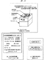
その対策としては、例えば図12に示すように、後洗浄処理が終了した基板(ウエハ)1を収納したウエハケース40を保管ボックス41内に保管し、酸素や水分との接触を避けるために、実質的に水分を含まない窒素などの非酸化性ガスを保管ボックス41内に供給しながら基板(ウエハ)1を保管する方法が考えられる。この場合、保管ボックス41の中に除湿剤42を入れたり、図13に示すように、ウエハケース40の中にも除湿剤42を入れたりすれば、Cu配線30の酸化や腐蝕の進行をさらに有効に抑制することができる。また、後洗浄処理からキャップ絶縁膜31の堆積までを4日以内に完了させる場合であっても、その間にCu配線30の表面がクリーンルーム内の空気に曝されていると、前述したCuイオンの発生を誘発するので好ましくない。従って、この場合でも、基板(ウエハ)1を収納したウエハケース40を上記のような保管ボックス41内に保管する方法は有効である。
後洗浄処理工程からキャップ絶縁膜31の堆積工程までの期間が4日を経過してしまった場合の他の対策として、基板1を後洗浄処理工程に再度搬送して表面洗浄を行った後、キャップ絶縁膜31を堆積する方法も有効である。この場合、再洗浄処理を行った基板1を長時間クリーンルーム内に放置すれば、Cu配線30の表面が再び酸化、腐蝕してしまうため、この再洗浄処理は、キャップ絶縁膜31を堆積する直前に行うことが望ましい。また、再洗浄処理の終わった基板1をやむを得ず一時的に放置する場合でも、前述した保管ボックス41内に保管しておくことによって、Cu配線30の表面の再酸化、腐蝕を最小限に止めることができる。
また、上記した再洗浄処理に代えて、前述した水素アニール処理を再度行ってCu配線30の表面を還元した後、キャップ絶縁膜31の堆積を行ってもよい。その際、基板1を放置する時間が長くなると予想される場合には、水素アニールを所定時間毎に繰り返して行うことが有効である。また、この水素アニール処理と前記の再洗浄処理や還元性プラズマ処理などを組み合わせて実施してもよい。
また、基板1を化学的機械研磨工程に再度搬送してCu配線30の表面を薄く研磨し、続いて前記の後洗浄処理および水素アニール処理を行ってからキャップ絶縁膜31の堆積を行ってもよい。あるいは、基板1をフッ酸(DHF)で洗浄して表面の酸化物やCu粒などを除去した後、キャップ絶縁膜31の堆積を行ってもよい。ただし、化学的機械研磨を再度実施する方法やフッ酸を使用する再洗浄方法を用いる場合は、Cu配線30それ自体も削るので、その断面積が小さくなり、電気抵抗が大きくなる虞れがあるため注意を要する。
後洗浄処理工程からキャップ絶縁膜31の堆積工程までの期間が4日を経過した基板1に対して、上記のような再生処理を施すことにより、TDDB寿命の劣化を最小限に止め、LSIの信頼性、製造歩留まりを確保することができる。なお、上記した再生処理は、その内のいずれか一つを単独で実施してもよいが、複数の処理を組み合わせて実施してもよい。
このように、実際のLSI製造ラインでは、後洗浄処理工程からキャップ絶縁膜31の堆積工程までの放置期間が4日以内となるような管理システムを採用すると共に、この放置期間が4日を経過した基板1に対しては、速やかに上記のような再生処理を実施するような管理システムを採用する必要がある。また、Cu配線形成工程を有するLSIの製造ラインが工場内に複数ある場合には、それぞれの製造ラインにおいて、後洗浄処理工程からキャップ絶縁膜31の堆積工程までの放置期間が4日以内となるような管理システムと、放置期間が4日を経過した基板1に対して再生処理を実施するような管理システムとを採用する必要がある。
後洗浄処理からキャップ絶縁膜31の堆積までの放置時間を管理する手法としては、例えば図14(a)、(b)に示すように、後洗浄処理が終了した基板(ウエハ)1を収納する前記のウエハケース40や保管ボックス41の表面に、通常の工程コントロールカードやロット番号表示カードなどと共に、放置時間コントロールカードを貼り付け、これに化学的機械研磨処理および後洗浄処理が完了した日時や放置可能時間などを記入して管理する方法が考えられる。
また、管理ミスや作業ミスを確実に防止するためには、上記のような放置時間コントロールカードとは別に、例えば図14(c)に示すような、放置日数や、再生処理中であるか否かが一目で分かる放置日数/再生表示カードなどを作成しておいたり、図15に示すように、ウエハケース40や保管ボックス41を保管するクリーンルーム内のウエハケース置き場に放置日数や再生処理の要否などを記載した表示カードを設置したりすることが有効である。
また、工場内の全ての製造ラインを管理するホストコンピュータには、図16に示すように、例えば化学的機械研磨処理および後洗浄処理が終了してからキャップ絶縁膜31を堆積するまでの放置時間や、再生処理の有無などのデータを入力しておき、ロットの進行を管理するコンピュータ端末に画面上にこれらのデータを表示できるような管理システムを構築する。
そして、例えば放置時間が4日を経過しているにもかかわらず再生処理が行われていない場合は、キャップ絶縁膜31の堆積を禁止する警告をコンピュータ端末に表示したり、放置時間が4日に近付くとコンピュータ端末にその旨を表示したり、警告音を発したりする機能を持たせることによって、管理ミスや作業ミスをより確実に防止することができる。
図17に示すように、上記した本実施の形態の管理手法を導入した結果、Cu配30線のTDDB寿命の劣化を有効に抑制することができた。
以上、本発明者によってなされた発明を実施の形態に基づき具体的に説明したが、本発明は前記実施の形態に限定されるものではなく、その要旨を逸脱しない範囲で種々変更可能であることはいうまでもない。
産業上の利用可能性
化学的機械研磨法を用いて絶縁膜の開口部内に銅を主成分として含む配線を形成した後、前記配線の表面をキャップ絶縁膜で覆う際、配線の形成からキャップ絶縁膜の堆積までを4日以内に実施することにより、Cu配線のTDDB寿命の低下を抑制することができる。
【図面の簡単な説明】
図1は、本発明の一実施の形態である半導体集積回路装置の製造方法を示す半導体基板の要部断面図である。
図2は、本発明の一実施の形態である半導体集積回路装置の製造方法を示す半導体基板の要部断面図である。
図3は、本発明の一実施の形態である半導体集積回路装置の製造方法を示す半導体基板の要部断面図である。
図4は、本発明の一実施の形態である半導体集積回路装置の製造方法を示す半導体基板の要部断面図である。
図5は、本発明の一実施の形態である半導体集積回路装置の製造方法を示す半導体基板の要部断面図である。
図6は、本発明の一実施の形態である半導体集積回路装置の製造方法を示す半導体基板の要部断面図である。
図7は、本発明の一実施の形態である半導体集積回路装置の製造方法を示す半導体基板の要部断面図である。
図8は、化学的機械研磨後の後洗浄処理を行った後、キャップ絶縁膜を堆積するまでの基板放置日数と破壊電界強度との関係を実測したグラフである。
図9は、図8の測定に用いたサンプルのTDDB寿命の放置時間依存性を示すグラフである。
図10は、化学的機械研磨後の後洗浄処理を行った後、キャップ絶縁膜を堆積するまでの基板放置日数と破壊電界強度との関係を2種類のキャップ絶縁膜を使って実測したグラフである。
図11は、本発明者が考察した放置時間によるTDDB寿命の劣化モデルを示す模式図である。
図12は、後洗浄処理が終了した半導体基板の保管方法の一例を示す説明図である。
図13は、後洗浄処理が終了した半導体基板の保管方法の一例を示す説明図である。
図14(a)、(b)、(c)は、後洗浄処理からキャップ絶縁膜の堆積までの基板管理方法の一例を示す説明図である。
図15は、後洗浄処理からキャップ絶縁膜の堆積までの基板管理方法の一例を示す説明図である。
図16は、後洗浄処理からキャップ絶縁膜の堆積までの基板管理方法の一例を示す説明図である。
図17は、本発明の一実施の形態である半導体基板の管理方法を導入して製造したCu配線のTDDB寿命を示すグラフである。Technical field
The present invention relates to a technology for manufacturing a semiconductor integrated circuit device, and in particular, a semiconductor having a step of forming an embedded wiring made of a conductive film containing copper (Cu) as a main component by using a chemical mechanical polishing method. The present invention relates to a technique effective when applied to the manufacture of an integrated circuit device.
Background art
The embedded wiring structure on the semiconductor substrate is obtained by embedding a wiring metal film in a wiring embedding opening such as a wiring groove or hole formed in an insulating film, and then chemically mechanically polishing an unnecessary metal film outside the opening. It is formed by a damascene wiring technique called single-damascene or dual-damascene that is removed by the method.
However, when the metal film is copper (Cu), Cu wiring is not in direct contact with the insulating film because it is more easily diffused into the insulating film than other metal films for wiring such as aluminum (Al). Thus, by covering the bottom and side surfaces of the Cu wiring with a thin barrier metal film and covering the surface of the Cu wiring with a cap insulating film, Cu atoms in the Cu wiring are prevented from diffusing into the surrounding insulating film. Yes.
Techniques for preventing Cu atoms in the Cu wiring from diffusing into the surrounding insulating film are described in Japanese Patent Application Laid-Open Nos. 11-1111843 and 10-50632. Among them, Japanese Patent Application Laid-Open No. 11-1111843 discloses a structure in which the upper surface of the Cu wiring is formed lower than the upper surface of the insulating film and the barrier insulating film is embedded therein. Japanese Patent Laid-Open No. 10-50632 discloses a structure in which the upper surfaces of the Cu wiring and the barrier metal film are formed lower than the upper surface of the insulating film, and the barrier insulating film is embedded therein.
Disclosure of the invention
In the LSI under development by the present inventor, Cu wiring is generally formed by the following process.
First, after forming an opening in an insulating film deposited on a semiconductor substrate (wafer), a barrier metal film made of a titanium nitride film or the like is thinly deposited on the insulating film including the inside of the opening, and then barrier metal A Cu film having a film thickness thicker than the depth of the opening is deposited on the upper part. Next, an unnecessary Cu film and barrier metal film outside the opening are removed by a chemical mechanical polishing method, thereby forming a Cu wiring inside the opening.
Next, the semiconductor substrate on which the Cu wiring is formed is transferred to a cleaning processing unit, and cleaning (hereinafter referred to as post-cleaning) is performed to remove foreign matters such as slurry adhering to the surface of the semiconductor substrate in the polishing process. .
The post-cleaning process includes an alkali cleaning process and a subsequent acid cleaning process. The alkali cleaning treatment is intended to neutralize an acidic slurry containing an oxidizing agent attached to the surface of the semiconductor substrate, and cleans the surface of the semiconductor substrate while supplying a weak alkaline chemical solution. The purpose of the acid cleaning treatment is to remove residual metal, reduce dangling bonds on the surface of the insulating film, and remove irregularities on the surface of the insulating film. Clean the surface.
When the acid contained in the chemical solution is a strong acid such as dilute hydrofluoric acid (DHF), not only the thin oxide layer (CuO) on the surface of the Cu wiring generated by the chemical mechanical polishing process is removed. Since the Cu wiring itself is also etched, the cross-sectional area of the Cu wiring may be reduced and the electrical resistance may be increased. Therefore, particularly when the line width of the Cu wiring is fine, it is desirable to use a chemical solution containing a weak acid such as an organic acid. However, when cleaning is performed with a chemical solution containing an organic acid, the oxide layer (CuO) on the surface of the Cu wiring is not removed. Therefore, it is necessary to perform a reduction treatment such as hydrogen annealing after the cleaning to remove the oxide layer (CuO). There is.
Next, a cap insulating film made of a silicon nitride film or the like is deposited on the surface of the semiconductor substrate after the post-cleaning process using a plasma CVD method or the like.
Here, when the semiconductor substrate (wafer) is left in the clean room between the end of the post-cleaning process and the deposition of the cap insulating film, the Cu wiring is obtained after a predetermined time has elapsed. The phenomenon that the lifetime of TDDB (Time Dependence on Dielectric Breakdown) of the present invention rapidly decreases was found. The TDDB life is a measure for objectively measuring the time dependency of dielectric breakdown, and a relatively high voltage is applied between Cu wires under a measurement condition of a predetermined temperature (for example, 140 ° C.). A time (life) obtained by creating a graph in which the time until dielectric breakdown is plotted against the applied electric field and extrapolating from this graph to the actual electric field strength (for example, 0.2 MV / cm).
Therefore, when forming the Cu wiring on the semiconductor substrate, it is necessary to take some measures to prevent the TDDB life of the Cu wiring from being reduced between the post-cleaning process after polishing and the deposition of the cap insulating film.
The objective of this invention is providing the technique which can suppress the fall of the TDDB lifetime of Cu wiring.
The above and other objects and novel features of the present invention will be apparent from the description of this specification and the accompanying drawings.
Of the inventions disclosed in this application, the outline of typical ones will be briefly described as follows.
According to another aspect of the present invention, there is provided a method for manufacturing a semiconductor integrated circuit device, comprising: (a) forming a first insulating film on a semiconductor substrate and then forming an opening for embedding a wiring in the first insulating film; ) Depositing a conductive film containing Cu as a main component on the first insulating film including the inside of the opening; and (c) chemically and mechanically polishing the conductive film and leaving it in the opening. Forming a Cu wiring in the opening; (d) cleaning the surface of the semiconductor substrate after the step (c); and (e) after the step (d), on the semiconductor substrate. Depositing a second insulating film on the surface of the Cu wiring to cover the surface of the Cu wiring with the second insulating film, and after the step (d) is completed, the step (e) is performed within 4 days. The production line is managed as implemented.
BEST MODE FOR CARRYING OUT THE INVENTION
Hereinafter, embodiments of the present invention will be described in detail with reference to the drawings. Note that components having the same function are denoted by the same reference symbols throughout the drawings for describing the embodiments, and the repetitive description thereof is omitted.
This embodiment is applied to an LSI manufacturing method in which a Cu wiring is formed on a complementary MISFET (Complementary Metal Insulator Semiconductor Field Effect Transistor) formed on a semiconductor substrate. This LSI manufacturing method will be described with reference to the drawings.
First, as shown in FIG. 1, a wafer-like semiconductor substrate (hereinafter referred to as a substrate, sometimes referred to as a wafer) 1 made of single crystal silicon is prepared, and an
In order to form the
The n-channel type MISFET Qn and the p-channel type MISFET Qp may be formed using any known process. For example, they are formed as follows. First, by subjecting the
Next, phosphorus or arsenic is ion-implanted into the p-
Next, after cleaning the surface of the
Next, as shown in FIG. 2, a first-layer W (tungsten)
In order to form the
The
In order to form the
Next, a W film is deposited on the
Next, as shown in FIG. 3, two layers of insulating
Here, the lower insulating
The insulating
In order to form the
Next, as shown in FIG. 4, two layers of insulating
Of the two insulating
Next, as shown in FIG. 5, after depositing a
The
When the
Next, as shown in FIG. 6, the
The polishing of the
The composition of the abrasive-free slurry is a mixture of pure water with an oxidizing agent, an organic acid and a corrosion inhibitor. As an oxidizing agent, hydrogen peroxide (H 2 O 2 ), Ammonium hydroxide, ammonium nitrate, ammonium chloride and the like. Examples of organic acids include citric acid, malonic acid, fumaric acid, malic acid, adipic acid, benzoic acid, phthalic acid, tartaric acid, lactic acid, succinic acid And oxalic acid. Of the above oxidizing agents, hydrogen peroxide does not contain a metal component and is not a strong acid. Of the above organic acids, citric acid is also commonly used as a food additive, has low toxicity, low harm as a waste liquid, no odor, and high solubility in water. Suitable organic acids.
Examples of the anticorrosive include BTA derivatives such as benzotriazole (BTA) and BTA carboxylic acid, dodecyl mercaptan, triazole, and tolyltriazole. Especially when benzotriazole is used, the surface of the
When chemical mechanical polishing is performed using the abrasive free slurry, the surface of the
As the polishing of the
Next, anticorrosion treatment is performed on the surface of the
Next, the
The
The post-cleaning process includes an alkali cleaning process and a subsequent acid cleaning process. The alkali cleaning is performed to neutralize an acidic slurry containing an oxidant attached to the surface of the
The acid cleaning after the alkali cleaning is intended to improve TDDB characteristics, remove residual metal, reduce dangling bonds on the surface of the insulating
The post-cleaning treatment can be performed by combining alkali cleaning using ammonium hydroxide and acid cleaning using dilute hydrofluoric acid (DHF). In this case, since the hydrofluoric acid is stronger than the organic acid, the thin oxide layer (CuO) on the surface of the
On the other hand, when acid cleaning is performed using an aqueous solution containing an organic acid, the oxide layer (CuO) on the surface of the
An organic acid and dilute hydrofluoric acid (DHF) are used as acid cleaning chemicals for removing foreign matters remaining on the surface of the
When the mixed aqueous solution having the above composition is used, the etching rate of Cu can be suppressed to 3 nm / or less and the etching rate of silicon oxide constituting the insulating
An aqueous solution (a mixed aqueous solution of organic acid, dilute hydrofluoric acid, and ammonium hydroxide) obtained by adding ammonia to the above mixed aqueous solution of organic acid and dilute hydrofluoric acid can also be used. In this case, each concentration of organic acid, hydrofluoric acid, and ammonium hydroxide is about 0.1 to 1%. Since this mixed aqueous solution has a pH of about 6 to 8, it is a neutral aqueous solution compared to an acidic aqueous solution. Therefore, the protective effect of the surface of the
In addition,% which shows the density | concentration of the aqueous solution which added said hydrofluoric acid, organic acid, and ammonia means weight%.
When hydrogen annealing is performed on the
The hydrogen annealing process is a process for reducing and removing the oxide layer (CuO) on the surface of the
Next, as shown in FIG. 7, the surface of the
The
By subjecting the surface of the
According to the knowledge obtained by the present inventor, in order to prevent a decrease in the TDDB life, a series of processes from the post-cleaning process after the chemical mechanical polishing process to the deposition of the
FIG. 8 shows a substrate after the post-cleaning process after chemical mechanical polishing (CMP) is performed using the above-mentioned aminoethanol aqueous solution (DAE) and CIREX, and then the
FIG. 9 is a graph showing the dependence of the TDDB life of the same sample on the standing time. As shown in the figure, the TDDB life from the first day to the fourth day is the same, but it decreases by about 3 digits between the 4th and 5th days, and about 3 digits between the 5th and 6th days. It has been found that the TDDB life is drastically reduced after 4 days after being left, such as a decrease of about 3 digits between the 6th and 11th days.
Next, FIG. 10 shows the result of the same measurement performed by changing the material of the
FIG. 11 shows a deterioration model of the TDDB life due to the standing time considered by the present inventors from the above measurement results.
When the surface of the
From the above examination results, the time from the post-cleaning process after the chemical mechanical polishing process to the deposition of the
Further, in an actual LSI manufacturing line, there may be a case where the manufacturing line must be temporarily stopped due to an unexpected situation such as a device failure or a failure. Therefore, even if the line is managed so that the process from the post-cleaning process to the deposition process of the
As a countermeasure, for example, as shown in FIG. 12, a
As another countermeasure when the period from the post-cleaning process to the deposition process of the
Further, instead of the re-cleaning process described above, the above-described hydrogen annealing process may be performed again to reduce the surface of the
Alternatively, the
By performing the above-described regeneration process on the
As described above, in an actual LSI manufacturing line, a management system is adopted in which the leaving period from the post-cleaning process to the deposition process of the
As a method for managing the standing time from the post-cleaning process to the deposition of the
Further, in order to surely prevent management mistakes and work mistakes, apart from the leaving time control card as described above, for example, as shown in FIG. As shown in FIG. 15, the number of days to be left / regeneration display card etc. can be prepared at a glance, or as shown in FIG. It is effective to install a display card that states whether or not.
In addition, as shown in FIG. 16, the host computer that manages all the production lines in the factory has a standing time from the completion of the chemical mechanical polishing process and the post-cleaning process until the
For example, if the regeneration process is not performed even though the leaving time has passed 4 days, a warning prohibiting the deposition of the
As shown in FIG. 17, as a result of introducing the management method of the present embodiment described above, it was possible to effectively suppress the deterioration of the TDDB life of the
As mentioned above, the invention made by the present inventor has been specifically described based on the embodiment. However, the present invention is not limited to the embodiment, and various modifications can be made without departing from the scope of the invention. Needless to say.
Industrial applicability
After the wiring containing copper as a main component is formed in the opening of the insulating film using the chemical mechanical polishing method, when covering the surface of the wiring with the cap insulating film, the process from the formation of the wiring to the deposition of the cap insulating film is 4 By carrying out within a day, the fall of the TDDB life of Cu wiring can be suppressed.
[Brief description of the drawings]
FIG. 1 is a fragmentary cross-sectional view of a semiconductor substrate showing a method of manufacturing a semiconductor integrated circuit device according to an embodiment of the present invention.
FIG. 2 is a fragmentary cross-sectional view of a semiconductor substrate showing a method for manufacturing a semiconductor integrated circuit device according to an embodiment of the present invention.
FIG. 3 is a fragmentary cross-sectional view of a semiconductor substrate showing a method of manufacturing a semiconductor integrated circuit device according to an embodiment of the present invention.
FIG. 4 is a fragmentary cross-sectional view of a semiconductor substrate showing a method of manufacturing a semiconductor integrated circuit device according to an embodiment of the present invention.
FIG. 5 is a fragmentary cross-sectional view of a semiconductor substrate showing a method for manufacturing a semiconductor integrated circuit device according to an embodiment of the present invention.
FIG. 6 is a fragmentary cross-sectional view of a semiconductor substrate showing a method for manufacturing a semiconductor integrated circuit device according to an embodiment of the present invention.
FIG. 7 is a fragmentary cross-sectional view of a semiconductor substrate showing a method for manufacturing a semiconductor integrated circuit device according to an embodiment of the present invention.
FIG. 8 is a graph obtained by actually measuring the relationship between the number of days the substrate is left until the cap insulating film is deposited after the post-cleaning process after the chemical mechanical polishing and the breakdown electric field strength.
FIG. 9 is a graph showing the dependence of the TDDB life of the sample used in the measurement of FIG. 8 on the standing time.
FIG. 10 is a graph obtained by actually measuring the relationship between the number of days the substrate is left until the cap insulating film is deposited and the breakdown electric field strength after performing the post-cleaning process after chemical mechanical polishing using two types of cap insulating films. is there.
FIG. 11 is a schematic diagram showing a deterioration model of the TDDB life due to the standing time considered by the present inventor.
FIG. 12 is an explanatory diagram showing an example of a method for storing a semiconductor substrate after the post-cleaning process.
FIG. 13 is an explanatory diagram illustrating an example of a method for storing a semiconductor substrate after the post-cleaning process.
14A, 14B, and 14C are explanatory diagrams illustrating an example of a substrate management method from post-cleaning processing to deposition of a cap insulating film.
FIG. 15 is an explanatory diagram showing an example of a substrate management method from post-cleaning processing to deposition of a cap insulating film.
FIG. 16 is an explanatory diagram showing an example of a substrate management method from post-cleaning processing to deposition of a cap insulating film.
FIG. 17 is a graph showing the TDDB life of Cu wiring manufactured by introducing the semiconductor substrate management method according to one embodiment of the present invention.
Claims (28)
(b)前記開口部内を含む前記第1絶縁膜上に銅を主成分として含む導電膜を形成する工程、
(c)前記導電膜を化学的および機械的に研磨して前記開口部内に残すことにより、前記開口部内に前記導電膜からなる配線を形成する工程、
(d)前記(c)工程の後、前記半導体基板の表面を洗浄する工程、
(e)前記(d)工程の後、前記半導体基板上に第2絶縁膜を形成することによって、前記配線の上面を前記第2絶縁膜で被覆する工程を含み、
前記(d)工程の終了後、4日以内に前記(e)工程を実施することを特徴とする半導体集積回路装置の製造方法。(A) forming an opening for embedding wiring in the first insulating film after forming the first insulating film on the semiconductor substrate;
(B) forming a conductive film containing copper as a main component on the first insulating film including the inside of the opening;
(C) forming a wiring made of the conductive film in the opening by chemically and mechanically polishing the conductive film and leaving it in the opening;
(D) a step of cleaning the surface of the semiconductor substrate after the step (c);
(E) After the step (d), including a step of covering the upper surface of the wiring with the second insulating film by forming a second insulating film on the semiconductor substrate,
A method of manufacturing a semiconductor integrated circuit device, wherein the step (e) is performed within 4 days after the completion of the step (d).
(a)半導体基板上に第1絶縁膜を形成した後、前記第1絶縁膜に配線埋込み用の開口部を形成する工程、
(b)前記開口部内を含む前記第1絶縁膜上に銅を主成分として含む導電膜を形成する工程、
(c)前記導電膜を化学的および機械的に研磨して前記開口部内に残すことにより、前記開口部内に前記導電膜からなる配線を形成する工程、
(d)前記(c)工程の後、前記半導体基板の表面を洗浄する工程、
(e)前記(d)工程の後、前記半導体基板の表面を再洗浄する工程、
(f)前記(e)工程の後、前記半導体基板上に第2絶縁膜を形成することによって、前記配線の上面を前記第2絶縁膜で被覆する工程。Manufacturing method of semiconductor integrated circuit device including the following steps (a) to (f):
(A) forming an opening for embedding wiring in the first insulating film after forming the first insulating film on the semiconductor substrate;
(B) forming a conductive film containing copper as a main component on the first insulating film including the inside of the opening;
(C) forming a wiring made of the conductive film in the opening by chemically and mechanically polishing the conductive film and leaving it in the opening;
(D) a step of cleaning the surface of the semiconductor substrate after the step (c);
(E) After the step (d), re-cleaning the surface of the semiconductor substrate;
(F) A step of coating the upper surface of the wiring with the second insulating film by forming a second insulating film on the semiconductor substrate after the step (e).
(a)半導体基板上に第1絶縁膜を堆積した後、前記第1絶縁膜に配線埋込み用の開口部を形成する工程、
(b)前記開口部内を含む前記第1絶縁膜上に銅を主成分として含む導電膜を堆積する工程、
(c)前記導電膜を化学的および機械的に研磨して前記開口部内に残すことにより、前記開口部内に前記導電膜からなる配線を形成する工程、
(d)前記(c)工程の後、前記半導体基板の表面を洗浄する工程、
(e)前記(d)工程の後、前記半導体基板の表面を水素アニール処理する工程、
(f)前記(e)工程の後、前記半導体基板上に第2絶縁膜を堆積することによって、前記配線の上面を前記第2絶縁膜で被覆する工程。Manufacturing method of semiconductor integrated circuit device including the following steps (a) to (f):
(A) after depositing a first insulating film on a semiconductor substrate, forming a wiring-embedded opening in the first insulating film;
(B) depositing a conductive film containing copper as a main component on the first insulating film including the inside of the opening;
(C) forming a wiring made of the conductive film in the opening by chemically and mechanically polishing the conductive film and leaving it in the opening;
(D) a step of cleaning the surface of the semiconductor substrate after the step (c);
(E) a step of hydrogen annealing the surface of the semiconductor substrate after the step (d);
(F) A step of coating the upper surface of the wiring with the second insulating film by depositing a second insulating film on the semiconductor substrate after the step (e).
(a)半導体基板上に第1絶縁膜を堆積した後、前記第1絶縁膜に配線埋込み用の開口部を形成する工程、
(b)前記開口部内を含む前記第1絶縁膜上に銅を主成分として含む導電膜を堆積する工程、
(c)前記導電膜を化学的および機械的に研磨して前記開口部内に残すことにより、前記開口部内に前記導電膜からなる配線を形成する工程、
(d)前記(c)工程の後、前記半導体基板の表面を洗浄する工程、
(e)前記(d)工程の後、前記半導体基板の表面を化学的および機械的に研磨する工程、
(f)前記(e)工程の後、前記半導体基板の表面を洗浄する工程、
(g)前記(f)工程の後、前記半導体基板上に第2絶縁膜を堆積することによって、前記配線の上面を前記第2絶縁膜で被覆する工程。Manufacturing method of semiconductor integrated circuit device including the following steps (a) to (g):
(A) after depositing a first insulating film on a semiconductor substrate, forming a wiring-embedded opening in the first insulating film;
(B) depositing a conductive film containing copper as a main component on the first insulating film including the inside of the opening;
(C) forming a wiring made of the conductive film in the opening by chemically and mechanically polishing the conductive film and leaving it in the opening;
(D) a step of cleaning the surface of the semiconductor substrate after the step (c);
(E) a step of chemically and mechanically polishing the surface of the semiconductor substrate after the step (d);
(F) a step of cleaning the surface of the semiconductor substrate after the step (e);
(G) A step of coating the upper surface of the wiring with the second insulating film by depositing a second insulating film on the semiconductor substrate after the step (f).
(b)前記開口部内を含む前記第1絶縁膜上に銅を主成分として含む導電膜を堆積する工程、
(c)前記導電膜を化学的および機械的に研磨して前記開口部内に残すことにより、前記開口部内に前記導電膜からなる配線を形成する工程、
(d)前記(c)工程の後、前記半導体基板の表面を洗浄する工程、
(e)前記(d)工程の後、前記半導体基板上に第2絶縁膜を堆積することによって、前記配線の上面を前記第2絶縁膜で被覆する工程を含み、
前記複数枚の半導体基板のうち、前記(d)工程の終了後、所定時間以内に前記(e)工程を実施する半導体基板と、前記(d)工程の終了後、前記(e)工程の開始までに前記所定時間が経過した半導体基板とをそれぞれ管理する工程を含むことを特徴とする半導体集積回路装置の製造方法。(A) after depositing a first insulating film on a plurality of semiconductor substrates, forming a wiring embedding opening in the first insulating film;
(B) depositing a conductive film containing copper as a main component on the first insulating film including the inside of the opening;
(C) forming a wiring made of the conductive film in the opening by chemically and mechanically polishing the conductive film and leaving it in the opening;
(D) a step of cleaning the surface of the semiconductor substrate after the step (c);
(E) After the step (d), including a step of coating the upper surface of the wiring with the second insulating film by depositing a second insulating film on the semiconductor substrate,
Among the plurality of semiconductor substrates, a semiconductor substrate that performs the step (e) within a predetermined time after the completion of the step (d), and a start of the step (e) after the completion of the step (d). A method for manufacturing a semiconductor integrated circuit device, comprising the steps of managing each of the semiconductor substrates for which the predetermined time has passed.
(b)前記開口部内を含む前記第1絶縁膜上に銅を主成分として含む導電膜を形成する工程、
(c)前記導電膜を化学的および機械的に研磨して前記開口部内に残すことにより、前記開口部内に前記導電膜からなる配線を形成する工程、
(d)前記(c)工程の後、前記半導体基板の表面を洗浄する工程、
(e)前記(d)工程の後、前記半導体基板上に第2絶縁膜を形成することによって、前記配線の上面を前記第2絶縁膜で被覆する工程を含み、
前記(d)工程の終了から前記(e)工程の開始までの間、前記半導体基板を非酸化性ガス雰囲気中で保管することを特徴とする半導体集積回路装置の製造方法。(A) forming an opening for embedding wiring in the first insulating film after forming the first insulating film on the semiconductor substrate;
(B) forming a conductive film containing copper as a main component on the first insulating film including the inside of the opening;
(C) forming a wiring made of the conductive film in the opening by chemically and mechanically polishing the conductive film and leaving it in the opening;
(D) a step of cleaning the surface of the semiconductor substrate after the step (c);
(E) After the step (d), including a step of covering the upper surface of the wiring with the second insulating film by forming a second insulating film on the semiconductor substrate,
A method of manufacturing a semiconductor integrated circuit device, wherein the semiconductor substrate is stored in a non-oxidizing gas atmosphere from the end of the step (d) to the start of the step (e).
Applications Claiming Priority (3)
| Application Number | Priority Date | Filing Date | Title |
|---|---|---|---|
| JP2002073160 | 2002-03-15 | ||
| JP2002073160 | 2002-03-15 | ||
| PCT/JP2003/001233 WO2003079429A1 (en) | 2002-03-15 | 2003-02-06 | Production method for semiconductor integrated circuit device |
Publications (1)
| Publication Number | Publication Date |
|---|---|
| JPWO2003079429A1 true JPWO2003079429A1 (en) | 2005-07-21 |
Family
ID=28035226
Family Applications (1)
| Application Number | Title | Priority Date | Filing Date |
|---|---|---|---|
| JP2003577326A Pending JPWO2003079429A1 (en) | 2002-03-15 | 2003-02-06 | Manufacturing method of semiconductor integrated circuit device |
Country Status (3)
| Country | Link |
|---|---|
| JP (1) | JPWO2003079429A1 (en) |
| TW (1) | TW200402843A (en) |
| WO (1) | WO2003079429A1 (en) |
Families Citing this family (7)
| Publication number | Priority date | Publication date | Assignee | Title |
|---|---|---|---|---|
| TWI362415B (en) * | 2003-10-27 | 2012-04-21 | Wako Pure Chem Ind Ltd | Novel detergent and method for cleaning |
| JP2005317808A (en) * | 2004-04-28 | 2005-11-10 | Nitta Haas Inc | Polishing cloth for polishing thin film and method for polishing thin film using the same |
| US9653398B1 (en) * | 2015-12-08 | 2017-05-16 | Northrop Grumman Systems Corporation | Non-oxide based dielectrics for superconductor devices |
| US10608159B2 (en) | 2016-11-15 | 2020-03-31 | Northrop Grumman Systems Corporation | Method of making a superconductor device |
| US10763419B2 (en) | 2017-06-02 | 2020-09-01 | Northrop Grumman Systems Corporation | Deposition methodology for superconductor interconnects |
| US10985059B2 (en) | 2018-11-01 | 2021-04-20 | Northrop Grumman Systems Corporation | Preclean and dielectric deposition methodology for superconductor interconnect fabrication |
| CN115483216A (en) * | 2022-08-15 | 2022-12-16 | 上海华力集成电路制造有限公司 | BEOL Process Structure and Method for Improving Device Reliability |
Family Cites Families (7)
| Publication number | Priority date | Publication date | Assignee | Title |
|---|---|---|---|---|
| JPH1034522A (en) * | 1996-07-17 | 1998-02-10 | Nikon Corp | Polishing apparatus for CMP and apparatus system for CMP |
| JP4554011B2 (en) * | 1999-08-10 | 2010-09-29 | ルネサスエレクトロニクス株式会社 | Manufacturing method of semiconductor integrated circuit device |
| US6423200B1 (en) * | 1999-09-30 | 2002-07-23 | Lam Research Corporation | Copper interconnect seed layer treatment methods and apparatuses for treating the same |
| JP3705724B2 (en) * | 1999-11-19 | 2005-10-12 | Necエレクトロニクス株式会社 | Manufacturing method of semiconductor device |
| JP3869608B2 (en) * | 2000-01-25 | 2007-01-17 | Necエレクトロニクス株式会社 | Anticorrosive |
| US20010043989A1 (en) * | 2000-05-18 | 2001-11-22 | Masami Akimoto | Film forming apparatus and film forming method |
| JP2001338927A (en) * | 2000-05-29 | 2001-12-07 | Sony Corp | Method for manufacturing semiconductor device |
-
2003
- 2003-02-06 WO PCT/JP2003/001233 patent/WO2003079429A1/en not_active Ceased
- 2003-02-06 JP JP2003577326A patent/JPWO2003079429A1/en active Pending
- 2003-03-13 TW TW092105478A patent/TW200402843A/en unknown
Also Published As
| Publication number | Publication date |
|---|---|
| WO2003079429A1 (en) | 2003-09-25 |
| TW200402843A (en) | 2004-02-16 |
Similar Documents
| Publication | Publication Date | Title |
|---|---|---|
| KR100698987B1 (en) | Manufacturing Method of Semiconductor Integrated Circuit Device | |
| US7084063B2 (en) | Fabrication method of semiconductor integrated circuit device | |
| US6730594B2 (en) | Method for manufacturing semiconductor device | |
| JP4554011B2 (en) | Manufacturing method of semiconductor integrated circuit device | |
| US6890846B2 (en) | Method for manufacturing semiconductor integrated circuit device | |
| US6383928B1 (en) | Post copper CMP clean | |
| JP2003332426A (en) | Semiconductor device manufacturing method and semiconductor device | |
| JP2003051481A (en) | Method for manufacturing semiconductor integrated circuit device | |
| JP2005333104A (en) | Semiconductor substrate cleaning liquid composition, semiconductor substrate cleaning method, and semiconductor device manufacturing method | |
| JPWO2003079429A1 (en) | Manufacturing method of semiconductor integrated circuit device | |
| JP2003347299A (en) | Method for manufacturing semiconductor integrated circuit device | |
| JP2006179948A (en) | Semiconductor device and method of manufacturing device | |
| JP2002329780A (en) | Semiconductor device manufacturing method and semiconductor device | |
| JP2008141204A (en) | Manufacturing method of semiconductor integrated circuit device | |
| US8329584B2 (en) | Method of manufacturing semiconductor device | |
| KR100746895B1 (en) | Manufacturing Method of Semiconductor Integrated Circuit Device | |
| JP4535505B2 (en) | Manufacturing method of semiconductor device | |
| JP2003124311A (en) | Semiconductor device manufacturing method and semiconductor device | |
| US20080176405A1 (en) | Method of cleaning a surface of a cobalt-containing material, method of forming an opening to a cobalt-containing material, semiconductor processing method of forming an integrated circuit comprising a copper-containing conductive line, and a cobalt-containing film cleaning solution | |
| JP2008004615A (en) | Method and apparatus for forming wiring | |
| KR20090061354A (en) | Cleaning solution for removing impurities, substrate cleaning method and manufacturing method of semiconductor device using same | |
| JP2007005840A (en) | Method of manufacturing semiconductor integrated circuit device |