JP7702194B2 - Cache-inhibited write operations - Google Patents
Cache-inhibited write operations Download PDFInfo
- Publication number
- JP7702194B2 JP7702194B2 JP2022516628A JP2022516628A JP7702194B2 JP 7702194 B2 JP7702194 B2 JP 7702194B2 JP 2022516628 A JP2022516628 A JP 2022516628A JP 2022516628 A JP2022516628 A JP 2022516628A JP 7702194 B2 JP7702194 B2 JP 7702194B2
- Authority
- JP
- Japan
- Prior art keywords
- data
- request
- interconnect
- write request
- processing unit
- Prior art date
- Legal status (The legal status is an assumption and is not a legal conclusion. Google has not performed a legal analysis and makes no representation as to the accuracy of the status listed.)
- Active
Links
Images


Classifications
-
- G—PHYSICS
- G06—COMPUTING OR CALCULATING; COUNTING
- G06F—ELECTRIC DIGITAL DATA PROCESSING
- G06F12/00—Accessing, addressing or allocating within memory systems or architectures
- G06F12/02—Addressing or allocation; Relocation
- G06F12/08—Addressing or allocation; Relocation in hierarchically structured memory systems, e.g. virtual memory systems
- G06F12/0802—Addressing of a memory level in which the access to the desired data or data block requires associative addressing means, e.g. caches
- G06F12/0806—Multiuser, multiprocessor or multiprocessing cache systems
- G06F12/0811—Multiuser, multiprocessor or multiprocessing cache systems with multilevel cache hierarchies
-
- G—PHYSICS
- G06—COMPUTING OR CALCULATING; COUNTING
- G06F—ELECTRIC DIGITAL DATA PROCESSING
- G06F12/00—Accessing, addressing or allocating within memory systems or architectures
- G06F12/02—Addressing or allocation; Relocation
- G06F12/08—Addressing or allocation; Relocation in hierarchically structured memory systems, e.g. virtual memory systems
- G06F12/0802—Addressing of a memory level in which the access to the desired data or data block requires associative addressing means, e.g. caches
- G06F12/0844—Multiple simultaneous or quasi-simultaneous cache accessing
- G06F12/0846—Cache with multiple tag or data arrays being simultaneously accessible
-
- G—PHYSICS
- G06—COMPUTING OR CALCULATING; COUNTING
- G06F—ELECTRIC DIGITAL DATA PROCESSING
- G06F12/00—Accessing, addressing or allocating within memory systems or architectures
- G06F12/02—Addressing or allocation; Relocation
- G06F12/08—Addressing or allocation; Relocation in hierarchically structured memory systems, e.g. virtual memory systems
- G06F12/0802—Addressing of a memory level in which the access to the desired data or data block requires associative addressing means, e.g. caches
- G06F12/0888—Addressing of a memory level in which the access to the desired data or data block requires associative addressing means, e.g. caches using selective caching, e.g. bypass
-
- G—PHYSICS
- G06—COMPUTING OR CALCULATING; COUNTING
- G06F—ELECTRIC DIGITAL DATA PROCESSING
- G06F13/00—Interconnection of, or transfer of information or other signals between, memories, input/output devices or central processing units
- G06F13/14—Handling requests for interconnection or transfer
- G06F13/16—Handling requests for interconnection or transfer for access to memory bus
- G06F13/1605—Handling requests for interconnection or transfer for access to memory bus based on arbitration
- G06F13/1652—Handling requests for interconnection or transfer for access to memory bus based on arbitration in a multiprocessor architecture
-
- G—PHYSICS
- G06—COMPUTING OR CALCULATING; COUNTING
- G06F—ELECTRIC DIGITAL DATA PROCESSING
- G06F13/00—Interconnection of, or transfer of information or other signals between, memories, input/output devices or central processing units
- G06F13/14—Handling requests for interconnection or transfer
- G06F13/16—Handling requests for interconnection or transfer for access to memory bus
- G06F13/1668—Details of memory controller
-
- G—PHYSICS
- G06—COMPUTING OR CALCULATING; COUNTING
- G06F—ELECTRIC DIGITAL DATA PROCESSING
- G06F9/00—Arrangements for program control, e.g. control units
- G06F9/06—Arrangements for program control, e.g. control units using stored programs, i.e. using an internal store of processing equipment to receive or retain programs
- G06F9/46—Multiprogramming arrangements
- G06F9/54—Interprogram communication
- G06F9/542—Event management; Broadcasting; Multicasting; Notifications
-
- G—PHYSICS
- G11—INFORMATION STORAGE
- G11C—STATIC STORES
- G11C11/00—Digital stores characterised by the use of particular electric or magnetic storage elements; Storage elements therefor
- G11C11/21—Digital stores characterised by the use of particular electric or magnetic storage elements; Storage elements therefor using electric elements
- G11C11/34—Digital stores characterised by the use of particular electric or magnetic storage elements; Storage elements therefor using electric elements using semiconductor devices
- G11C11/40—Digital stores characterised by the use of particular electric or magnetic storage elements; Storage elements therefor using electric elements using semiconductor devices using transistors
- G11C11/401—Digital stores characterised by the use of particular electric or magnetic storage elements; Storage elements therefor using electric elements using semiconductor devices using transistors forming cells needing refreshing or charge regeneration, i.e. dynamic cells
- G11C11/4063—Auxiliary circuits, e.g. for addressing, decoding, driving, writing, sensing or timing
- G11C11/407—Auxiliary circuits, e.g. for addressing, decoding, driving, writing, sensing or timing for memory cells of the field-effect type
- G11C11/409—Read-write [R-W] circuits
-
- G—PHYSICS
- G06—COMPUTING OR CALCULATING; COUNTING
- G06F—ELECTRIC DIGITAL DATA PROCESSING
- G06F12/00—Accessing, addressing or allocating within memory systems or architectures
- G06F12/02—Addressing or allocation; Relocation
- G06F12/08—Addressing or allocation; Relocation in hierarchically structured memory systems, e.g. virtual memory systems
- G06F12/0802—Addressing of a memory level in which the access to the desired data or data block requires associative addressing means, e.g. caches
- G06F12/0806—Multiuser, multiprocessor or multiprocessing cache systems
- G06F12/0815—Cache consistency protocols
- G06F12/0831—Cache consistency protocols using a bus scheme, e.g. with bus monitoring or watching means
Landscapes
- Engineering & Computer Science (AREA)
- Theoretical Computer Science (AREA)
- Physics & Mathematics (AREA)
- General Engineering & Computer Science (AREA)
- General Physics & Mathematics (AREA)
- Software Systems (AREA)
- Microelectronics & Electronic Packaging (AREA)
- Computer Hardware Design (AREA)
- Multimedia (AREA)
- Memory System Of A Hierarchy Structure (AREA)
Description
本発明は、一般に、データ処理システムに関し、具体的には、データ処理システムにおける書き込みオペレーションに関する。さらにより具体的には、本発明は、データ処理システムにおけるキャッシュ禁止(cache-inhibited)書き込みオペレーションに関する。 The present invention relates generally to data processing systems, and more particularly to write operations in data processing systems. Even more particularly, the present invention relates to cache-inhibited write operations in data processing systems.
共有メモリ・マルチプロセッサ(MP)データ処理システムにおいて、システム内の複数のプロセッサの各々は、一般に、共有メモリに格納されたデータにアクセスし、変更することができる。共有メモリに格納されたデータへのアクセス待ち時間を低減するために、プロセッサは、典型的には、プロセッサによりアクセスされる可能性の高い、共有メモリから取得したデータをバッファする高速のローカル・キャッシュを備える。プロセッサの様々なローカル・キャッシュに保持されるデータの一貫したビューは、一貫性プロトコルの実装によって維持される。 In a shared memory multiprocessor (MP) data processing system, each of the multiple processors in the system can generally access and modify data stored in a shared memory. To reduce the latency of accessing data stored in the shared memory, the processors typically have high speed local caches that buffer data retrieved from the shared memory that is likely to be accessed by the processor. A consistent view of the data held in the various local caches of the processors is maintained by the implementation of a consistency protocol.
このような共有メモリMPシステムでは、例えば、共有メモリ内のページ・テーブルの適切な設定により、アドレス空間における特定のアドレスをキャッシュ禁止(キャッシュ不可能(non-cacheable))と指定することは一般的である。これらのキャッシュ禁止アドレスと関連付けられたデータは、プロセッサのローカル・キャッシュにキャッシュされることはない。キャッシュ禁止アドレスに対するデータのキャッシュを制限することによって、キャッシュ禁止アドレスと関連付けられたデータを変更しても、プロセッサのローカル・キャッシュに常駐するデータのあらゆる古いコピー又は複数のコピーの無効化を必要としないという点で、対応するメモリ位置のコンテンツの単一の一貫したビューの維持管理が、大幅に簡素化される。 In such shared-memory MP systems, it is common to designate certain addresses in the address space as non-cacheable, for example by appropriate configuration of page tables in the shared memory. Data associated with these non-cacheable addresses are never cached in the processor's local cache. By restricting the caching of data for non-cacheable addresses, maintaining a single consistent view of the contents of the corresponding memory locations is greatly simplified, in that modifications to the data associated with non-cacheable addresses do not require invalidation of any stale copies or copies of the data resident in the processor's local cache.
1つ又は複数の実施形態において、データ処理システムのアドレス・インターコネクト上で、書き込みデータをブロードキャストすることにより、キャッシュ禁止アドレスへの書き込みが促進される。 In one or more embodiments, writes to cache-inhibited addresses are facilitated by broadcasting the write data on the address interconnect of the data processing system.
例えば、少なくとも一実施形態において、データ処理システムは、ブロードキャスト・アドレス・インターコネクト及びデータ・インターコネクトを含むシステム・インターコネクトに結合された複数の処理ユニットを含む。処理ユニットは、メモリ・アクセス命令を実行するプロセッサ・コアと、プロセッサ・コアに結合され、プロセッサ・コアによるアクセスのためにデータを格納するように構成された、キャッシュ・メモリとを含む。処理ユニットは、アドレス・インターコネクト上で、システム・インターコネクトに結合された宛先デバイスに対するキャッシュ禁止書き込み要求及び書き込みデータをブロードキャストするように構成される。種々の実施形態において、最初のキャッシュ禁止要求及び書き込みデータは、アドレス・インターコネクト上の同じ又は異なる要求において通信することができる。 For example, in at least one embodiment, a data processing system includes a plurality of processing units coupled to a system interconnect including a broadcast address interconnect and a data interconnect. The processing units include a processor core for executing memory access instructions and a cache memory coupled to the processor core and configured to store data for access by the processor core. The processing units are configured to broadcast, on the address interconnect, a cache inhibit write request and write data to a destination device coupled to the system interconnect. In various embodiments, the initial cache inhibit request and write data can be communicated in the same or different requests on the address interconnect.
ここで図、特に図1を参照すると、一実施形態によるデータ処理システム100の高レベル・ブロック図が示される。図示のように、データ処理システム100は、データ及び命令を処理するための(少なくとも処理ユニット102a~102bを含む)複数の処理ユニット102を含む。処理ユニット102は、取り付けられたデバイス間でアドレス、データ及び制御情報を伝達するために、システム・インターコネクト(相互接続)104に通信するように結合される。好ましい実施形態では、システム・インターコネクト104は、分岐したアドレス・インターコネクト及びデータ・インターコネクトを含む。図3を参照して以下でさらに説明するように、要求及びコヒーレンス応答を伝達する、アドレス・インターコネクトは、全ての要求及びコヒーレンス応答を、全ての取り付けられたデバイスに伝達する、アドレス・バスなどのブロードキャスト・インターコネクトである場合にさらに好ましい。それとは対照的に、データ・インターコネクトが、データのソースから宛先への直接通信をサポートする、スイッチなどのポイント・ツー・ポイント・インターコネクトである場合は好ましい。
Now referring to the figures, and in particular to FIG. 1, a high level block diagram of a
示される実施形態では、システム・インターコネクト104に結合されたデバイスは、処理ユニット102だけでなく、共有システム・メモリ108へのインターフェースを提供するメモリ・コントローラ106、及び各々がそれぞれのメザニン(Mezzanine)バス112へのインターフェースを提供する1つ又は複数のホスト・ブリッジ110も含む。メザニン・バス112はまた、ネットワーク・インターフェース・カード、I/Oアダプタ、不揮発性メモリ、不揮発性ストレージ・デバイス・アダプタ、付加的なバス・ブリッジなどを含むことができる、図示されていない付加的なデバイスを取り付けるためのスロットも提供する。
In the embodiment shown, the devices coupled to the
さらに図1に示すように、単一の集積回路として実現することができる各処理ユニット102は、命令及びデータを処理するための1つ又は複数のプロセッサ・コア120を含む(その1つのみが明示的に示される)。各プロセッサ・コア120は、実行のために命令をフェッチして指示する命令シーケンシング・ユニット(ISU)122と、ISU122からディスパッチされた命令を実行するための1つ又は複数の実行ユニット124と、データ及び制御情報を一時的にバッファするためのレジスタ123のセットとを含む。実行ユニット124により実行される命令は、キャッシュ可能なアドレス及びキャッシュ不可能なアドレスと関連付けられたデータを読み書きするロード及びストア命令などのメモリ・アクセス命令を含む。
1, each processing unit 102, which may be implemented as a single integrated circuit, includes one or more processor cores 120 (only one of which is explicitly shown) for processing instructions and data. Each
各プロセッサ・コア120は、実行されたストア及びロード命令にそれぞれ対応するストア及びロード要求の完了を管理するための、L1ストア・キュー(STQ)127及びロード・ユニット128をさらに含む。一実施形態では、L1 STQ127は、複数のキュー・エントリを含む先入れ先出し(FIFO)キューとして実装することができる。従って、ストア要求は、ターゲット・アドレスを決定するために、対応するストア命令の実行時にL1 STQ127の「上部」エントリにロードされ、ストア要求がL1 STQ127の「底部」又は「コミット」エントリに到達したときに開始される。
Each
本出願は、ロード及びストア命令などの「命令」と、「要求」とを区別することに留意することが重要である。ロード及びストア「命令」は、本明細書では、命令のタイプを識別する要求コード(オペコード)と、アクセスされるデータもしくはそのアドレス又はその両方を指定する1つ又は複数のオペランドとを含む実行ユニットへの入力として定義される。ロード及びストア「要求」は、本明細書では、アクセスされる少なくともデータのターゲット・アドレスを指定する、命令実行に続いて生成されるデータもしくは信号又はその両方として定義される。従って、ロード及びストア要求は、データ・アクセスを開始するために、プロセッサ・コア120からメモリ・システムに伝送することができるが、ロード及びストア命令は伝送することができない。
It is important to note that this application distinguishes between "instructions", such as load and store instructions, and "requests". Load and store "instructions" are defined herein as inputs to an execution unit that include a request code (opcode) that identifies the type of instruction, and one or more operands that specify the data to be accessed and/or its address. Load and store "requests" are defined herein as data and/or signals generated following instruction execution that specify at least the target address of the data to be accessed. Thus, load and store requests may be transmitted from the
プロセッサ・コア120のオペレーションは、共有システム・メモリ108をその最下位に有し、かつ、示される実施形態においてはL1キャッシュ126及びL2キャッシュ130を含むキャッシュ・メモリの2つ又はそれより多いレベルをその上位に有する、マルチ・レベル揮発性メモリ階層によってサポートされる。他の共有メモリ・マルチプロセッサ・データ処理システムにおけるように、メモリ階層のキャッシュ可能なコンテンツは、一般に、データ処理システム100の任意の処理ユニット102における任意のプロセッサ・コア120で実行される実行スレッドによりアクセスし変更することができる。
The operation of the
一実施形態によれば、L1キャッシュ126はストア・スルー・キャッシュとして実装され、このことは、他のプロセッサ・コア120に対するキャッシュ・ヒーレンシのポイントがL1キャッシュ126の下に配置され、示される実施形態においては、ストア・インL2キャッシュ130に配置されることを意味する。従って、L1キャッシュ126は、そのキャッシュ・ラインについての真のキャッシュ・コヒーレンシ状態(例えば、変更済み(Modified)、排他的(Exclusive)、共有(Shared)、無効(Invalid)など)を維持せずに、有効/無効ビットを維持するのみである。L1キャッシュ126はストア・スルー・キャッシュとして実装されるので、ストア要求は、最初に、L1キャッシュ126内の関連付けられたプロセッサ・コア120に対して完了し、次いで、示される実施形態ではL2キャッシュ130である、システム全体のコヒーレンシのポイントで、他の処理ユニット102に対して完了する。
According to one embodiment, the L1 cache 126 is implemented as a store-through cache, which means that the point of cache coherency for
さらに図1に示すように、L2キャッシュ130は、命令及びデータのキャッシュ・ラインを、それぞれのメモリ・アドレス及びコヒーレンス状態と関連付けて格納するストレージ・アレイ及びディレクトリ140を含む。またL2キャッシュ130は、関連付けられたプロセッサ・コア120から受け取ったキャッシュ可能なメモリ・アクセス要求に独立して同時にサービスする、多数の読み出しクレーム(RC)状態機械142a~142nも含む。RC機械142は、ロード・バス160、イン・オーダL2ロード・キュー(LDQ)161、及びコマンド・バス162を介して、プロセッサ・コア120内のLDユニット128からコア・ロード要求を受け取る。同様に、RC機械142は、ストア・バス164、イン・オーダL2ストア・キュー(STQ)166、及びコマンド・バス162を介して、プロセッサ・コア120内のL1 STQ127からコア・ストア要求を受け取る。
1, the L2 cache 130 includes a storage array and
L2キャッシュ130はさらに、システム・インターコネクト104及びスヌープ・バス170を介して他の処理ユニット102から受け取ったキャッシュ可能なメモリ・アクセス及び他の要求にサービスするために、幾つかのスヌープ(SN)状態機械144a~144nを含む。SN機械144及びRC機械142はそれぞれ、バック無効化(back-invalidation)バス172に接続され、それにより、いずれのSN機械144又はRC機械142も、キャッシュ・ラインの無効化をプロセッサ・コア120に信号で送ることができる。
The L2 cache 130 further includes several snoop (SN)
少なくとも1つの実施形態において、L2キャッシュ130は、RC機械142及びSN機械144のうち、最大でも1つが、任意の時間に所与のターゲット・キャッシュ・ライン・アドレスをターゲットとする要求にアクティブにサービスできるように構築される。その結果、同じキャッシュ・ラインをターゲットとする第1の要求が、アクティブなRC機械142又はSN機械144によって既にサービスされている間に、第2の要求を受け取った場合、第1の要求のサービスが完了し、アクティブな状態機械がアイドル状態に戻るまで、後の第2の要求をキューに入れるか又は拒否する必要がある。 In at least one embodiment, the L2 cache 130 is constructed such that at most one of the RC machine 142 and the SN machine 144 can be actively servicing requests targeting a given target cache line address at any given time. As a result, if a second request is received while a first request targeting the same cache line is already being serviced by the active RC machine 142 or SN machine 144, the later second request must be queued or rejected until servicing of the first request is completed and the active state machine returns to the idle state.
L2キャッシュ130はさらに、プロセッサ・コア120から受け取ったキャッシュ禁止(CI)メモリ・アクセス要求にサービスするためのキャッシュ不可能ユニット(NCU)146を含む。NCU146は、キャッシュ不可能なアドレスをターゲットとする、関連付けられたプロセッサ・コア120から受け取ったメモリ・アクセス要求に独立して同時にサービスするための多数のNCUストア(NST)状態機械150a~150nを含む。NST機械150は、ストア・バス164及びイン・オーダNCUストア・キュー(NSQ)148を介して、プロセッサ・コア120内のL1 STQ127からコアCI書き込み要求を受け取る。さらに、NCU146は、ロード・バス160を介して、プロセッサ・コア120内のLDユニット128からコアCIの読み出し要求を受け取る、多数のNCUロード(NLD)状態機械152a~152nを含む。
The L2 cache 130 further includes a non-cacheable unit (NCU) 146 for servicing cache inhibited (CI) memory access requests received from the
当業者であれば、図1のデータ処理システム100は、インターコネクト・ブリッジ、不揮発性ストレージ、ネットワークもしくは取り付けられたデバイスに接続するためのポート等のような図示されていない多くの付加的なコンポーネントを含むことができることもさらに理解するであろう。このような付加的なコンポーネントは、説明される実施形態の理解には必要ないため、図1には示されておらず、本明細書でさらに論じられてもいない。しかしながら、本明細書で説明される拡張機能は、多様なアーキテクチャのデータ処理システムに適用可能であり、図1に示される一般化されたデータ処理システムのアーキテクチャに決して限定されないことも理解されたい。例えば、図1は、キャッシュ禁止要求にサービスするための別個のNCUを含む実施形態を示すが、他のアーキテクチャは、L2キャッシュ130内のキャッシュ論理などの他の論理を使用して、CI書き込みなどのキャッシュ禁止要求にサービスすることができる。
Those skilled in the art will further appreciate that
ここで図2を参照すると、一実施形態による宛先デバイス200のより詳細な図が示される。宛先デバイス200は、CI書き込み要求の宛先(ターゲット)として機能することができるシステム・インターコネクト104に結合された任意のデバイスとすることができる。例えば、図1の実施形態では、宛先デバイス200は、ホスト・ブリッジ110又はメモリ・コントローラ106とすることができる。 Referring now to FIG. 2, a more detailed diagram of a destination device 200 is shown according to one embodiment. Destination device 200 may be any device coupled to system interconnect 104 that may act as a destination (target) for a CI write request. For example, in the embodiment of FIG. 1, destination device 200 may be host bridge 110 or memory controller 106.
示される実施形態では、宛先デバイス200は、システム・インターコネクト104を形成するアドレス・インターコネクト202及びデータ・インターコネクト204の両方に結合される。前述のように、アドレス・インターコネクト202は、取り付けられたデバイスの各々が、アドレス・インターコネクト202上で伝送される全ての要求及びコヒーレンスメッセージに対する可視性をもつことを意味する、バスなどのブロードキャスト・インターコネクトであることが好ましい。一方、データ・インターコネクト204は、データ・パケットが経路指定される間、データ・パケットは、複数の(一般的には全てではない)スヌーパを送ることができるが、オペレーションの宛先だけが、データ・インターコネクト204上で伝送されるデータ・パケットを受け取り、処理することを意味する、ポイント・ツー・ポイント・インターコネクトとして実装されることが好ましい。示される実施形態では、宛先デバイス200は、他のコンポーネントの中で、アドレス・インターコネクト202上で受け取った要求をバッファするための複数のキュー・エントリ212a~212nを有する要求キュー210を含む。各キュー・エントリ212は、少なくとも、要求の宛先(ターゲット)アドレスをバッファするためのアドレス・フィールド214と、要求タイプ(例えば、読み出し、書き込みなど)の表示をバッファするための要求フィールド216と、要求と関連付けられたデータをバッファするためのデータ・フィールド218とを含む。さらに図2に示すように、宛先デバイス200はまた、アドレス・インターコネクト202及びデータ・インターコネクト204の両方からデータ・フィールド218内に入れられた情報を選択することができる選択論理220(マルチプレクサとして表される)を含む。
In the illustrated embodiment, the destination device 200 is coupled to both an
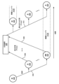
ここで図3を参照すると、一実施形態による、データ処理システム100のシステム・インターコネクト104上の例示的なオペレーションの時間空間図が示される。オペレーションは、RC機械142又はNST機械150などのマスタ300が、データ処理システム100のアドレス・インターコネクト202上で要求302を発行するときに開始する。要求302は、所望のアクセスのタイプを示すトランザクション・タイプと、要求によってアクセスされるリソースを示すリソース識別子(例えば、ターゲット実アドレス)とを含むことが好ましい。一般的なタイプの要求としては、以下の表Iに示すものを含むことが好ましい。

要求302は、宛先デバイス200(例えば、ホスト・ブリッジ110及びメモリ・コントローラ106)及びL2キャッシュ130のSN機械144などのスヌーパ304によって受け取られる。一般に、要求302は、処理ユニット102によって要求302に内部でサービスできない場合にのみ、アドレス・インターコネクト202上で伝送されるため、若干の例外はあるものの、要求302を開始するマスタと同じL2キャッシュ130内のSN機械144は、その要求302をスヌープしない(すなわち、一般に、自己スヌープはない)。
The
要求302を受け取ることに応答して、スヌーパ304は、アドレス・インターコネクト202上で、それぞれの部分応答(Presp)306を提供することができ、各Presp306は、要求302に対する少なくともそのスヌーパ304のコヒーレンス応答を表す。宛先デバイス200は、例えば、宛先デバイス200が要求アドレスをもたらすかどうか、及び宛先デバイス200が要求にサービスするために使用可能なリソースを有するかどうかに基づいて、(存在する場合には)その部分応答を決定する。L2キャッシュ130は、例えば、L2ストレージ・アレイ及びディレクトリ140の可用性、要求を処理するためのリソースの可用性(利用可能なSN機械144を含む)、L2ストレージ・アレイ及びディレクトリ140内の要求アドレスと関連付けられたキャッシュ状態に基づいて、部分応答306を決定することができる。
In response to receiving the
様々なスヌーパ304の部分応答は、応答論理308の1つ又は複数のインスタンスによって、段階的に又は一度に論理的に組み合わされ、要求302に対するシステム全体の組み合わせ応答(combined response)(Cresp)310が決定される。応答論理308は、要求302に対するシステム全体の応答(成功(Success)、再試行(Retry)など)を示すために、アドレス・インターコネクト202を介してマスタ300及びスヌーパ304に組み合わせ応答310を提供する。組み合わせ応答310が要求302の成功を示す場合、組み合わせ応答310は、例えば、書き込みデータについての宛先(該当する場合)、要求されたメモリ・ブロックがマスタ300によってキャッシュされたキャッシュ状態(該当する場合)、もしくは1つ又は複数のキャッシュ126、130内の要求されたメモリ・ブロックを無効にする「クリーンアップ(cleanup)」オペレーションが必要130とされるかどうか(該当する場合)又はそれらの組み合わせを示すことができる。
The partial responses of the
組み合わせ応答310を受け取ることに応答して、マスタ300及びスヌーパ304の1つ又は複数は、一般的には、要求302にサービスするために1つ又は複数のオペレーションを実行する。これらのオペレーションは、データをマスタ300へ供給すること、1つ又は複数のキャッシュ126、130にキャッシュされたデータを無効化する又は別の方法で更新すること、キャストアウト・オペレーションを実行すること、データをシステム・メモリ108又はI/Oデバイスへ書き込むことなどを含むことができる。さらに後述するように、応答論理210による組み合わせ応答310の生成前又は生成後に、データをマスタ300との間で伝送することができる。一般に、殆どのオペレーションでは、システム・インターコネクト104上のオペレーションと関連付けられたデータは、データ・インターコネクト204を介して伝送される。しかしながら、本明細書でさらに説明するように、少なくとも幾つかの実施形態においては、幾つかのオペレーションにおいて、データは、アドレス・インターコネクト202を介して伝送される。
In response to receiving the combined
要求に応答してスヌーパ304により提供される部分応答、及び要求に応答してスヌーパを実行したオペレーション、もしくはその組み合わせ応答又はそれらの組み合わせは、要求により指定されたターゲット・アドレスに関して、スヌーパがコヒーレンシの最高点(Highest Point of Coherency、HPC)であるか、コヒーレンシの最低点(Lowest Point of Coherency、LPC)であるか、又はそのどちらでもないかによって決まり得る。LPCは、本明細書では、メモリ・ブロックのためのリポジトリとして機能するメモリ・デバイス又はI/Oデバイスとして定義される。メモリ・ブロックのHPCが存在しない場合、LPCはメモリ・ブロックの真のイメージを保持し、メモリ・ブロックの付加的なキャッシュされたコピーを生成する要求を許可する又は拒否する権限を有する。図1及び図2のデータ処理システムにおける典型的な要求においては、LPCは、参照されるメモリ・ブロックのためのリポジトリとして機能するシステム・メモリ108のメモリ・コントローラ106、又はメモリ・マップトI/Oアドレスをもたらすホスト・ブリッジ110となる。HPCは、本明細書では、メモリ・ブロックの真のイメージをキャッシュし(LPCにおける対応するメモリ・ブロックと一致する場合又は一致しない場合もある)、メモリ・ブロックを変更する要求を許可する又は拒否する権限を有する、一意に識別されるデバイスとして定義される。記述的に、HPCは、メモリ・ブロックを変更しないオペレーションに応答して、メモリ・ブロックの共有コピーを要求側に提供することもできる。このように、図1及び図2のデータ処理システムの実施形態における典型的な要求において、HPCは、存在する場合には、L2キャッシュ230となる。他の指標を使用してメモリ・ブロックのHPCを指定することもできるが、本発明の好ましい実施形態は、L2キャッシュ130のディレクトリ内の選択されたキャッシュ状態を用いて、メモリ・ブロックのHPC(存在する場合)を指定する。
The partial response provided by the
さらに図3を参照すると、存在する場合には要求302内で参照したメモリ・ブロックに対するHPCは、又はHPCが存在しない場合にはメモリ・ブロックのLPCは、保護ウィンドウ312aの間、要求402に応答してメモリ・ブロックのコヒーレンス所有権の移転を防止する責任を有することが好ましい。図3に示す例示的なシナリオにおいては、要求302の要求アドレスが指定するメモリ・ブロックに対するHPCであるスヌーパ304は、少なくとも、スヌーパ304がその部分応答306を決定した時点からスヌーパ304が組み合わせ応答310を受け取るまで継続する保護ウィンドウ312aの間(及び場合によってはその後)、マスタ300への要求されたメモリ・ブロックの所有権の移転を必要に応じて防止する。保護ウィンドウ312aの間、スヌーパ304は、同じ要求アドレスを指定している他の要求に部分応答306(例えば、再試行Presp)を提供することによって所有権の移転を防止し、この部分応答306は、そうした所有権がマスタ300へ成功裡に移転されるまで、他のマスタがコヒーレンス所有権を取得することを防止する。マスタ300は同様に、組み合わせ応答310を受け取った後に要求302内で要求されたメモリ・ブロックの所有権を保護するために、保護ウィンドウ312bを開始する。
3, the HPC for the memory block referenced in
スヌーパ304は全て、上述のCPU及びI/Oの要求を処理するためのリソースが限られているので、幾つかの異なるレベルの部分応答及び対応する組み合わせ応答が可能である。例えば、要求されたメモリ・ブロックを担当するメモリ・コントローラ106が、要求を処理するために使用可能なキュー・エントリを有する場合には、メモリ・コントローラ106は、要求に対してLPCとして働くことができることを示す部分応答で応答することができる。一方、メモリ・コントローラ106が、要求を処理するために使用可能なキュー・エントリをもたない場合には、メモリ・コントローラ106は、メモリ・ブロックに対するLPCであることを示す部分応答で応答することができるが、現時点で要求にサービスすることはできない。同様に、L2キャッシュ130は、スヌープされた要求302を処理するために、使用可能なSN機械144を要求し、L2ストレージ・アレイ及びディレクトリ140へのアクセスすることがある。これらのリソースのいずれか(又は両方)にアクセスできない場合には、必要なリソースがないために要求にサービスできないこと(例えば、再試行)を知らせる部分応答(及び対応するCR)をもたらす。
Since all
ここで図4を参照すると、データ処理システムのシステム・インターコネクト上で、キャッシュ不可能ユニット(NCU)がキャッシュ禁止(CI)書き込み要求を発行する従来技術の方法の高レベル論理フローチャートが示される。理解を促進するために、図4の従来技術の方法は、図1の例示的なデータ処理システム100及び図3に示される例示的なオペレーションを参照して説明する。
Referring now to FIG. 4, there is shown a high level logical flow chart of a prior art method for a non-cacheable unit (NCU) to issue a cache inhibited (CI) write request on a system interconnect of a data processing system. To facilitate understanding, the prior art method of FIG. 4 will be described with reference to the exemplary
図4のプロセスは、ブロック400で開始し、次いで、NCU146のNST機械150が、ストア・バス164及びNSQ148を介して関連付けられたプロセッサ・コア120からCI書き込み要求を受け取ることを示す、ブロック402に進む。CI書き込み要求は、例えば、キャッシュ禁止メモリの領域をターゲットとするプロセッサ・コア120による対応するストア命令の実行によって生成され、少なくともターゲット・アドレス及び書き込みデータを含む。
The process of FIG. 4 begins at block 400 and then proceeds to block 402, which illustrates the NST machine 150 of the NCU 146 receiving a CI write request from an associated
CI書き込み要求を受け取ることに応答して、NST機械150は、アドレス・インターコネクト202上でCI書き込み要求を発行する(ブロック404)。図6Aに示すように、CI書き込み要求600は、少なくとも、要求をCI書き込み要求として識別する要求タイプ・フィールド602と、CI書き込み要求を発行する、処理ユニット102、NCU146、及びNST機械150を識別するマスタ・タグ・フィールド604と、関連付けられたプロセッサ・コア120によって提供されるターゲット・アドレスを指定するアドレス・フィールド606とを含む。
In response to receiving the CI write request, the NST machine 150 issues a CI write request on the address interconnect 202 (block 404). As shown in FIG. 6A, the
図3を参照して上述したように、CI書き込み要求に応答して、データ処理システム100内のスヌーパ304は、それぞれの部分応答(Presp)306を提供する。これらの部分応答306は論理的に組み合わされ、応答論理308のインスタンス(例えば、発行処理ユニット102内に常駐する)は、部分応答306に基づいて、CI書き込み要求に対する組み合わせ応答(Cresp)310を形成する。キャッシュ・スヌーパは、典型的には、キャッシュ禁止要求に対するヌル部分応答を生成し、キャッシュ禁止要求に対する付加的な処理を行わない。
As described above with reference to FIG. 3, in response to a CI write request, a
図6Bは、Presp306及びCresp310の両方に用いることができるコヒーレンス応答610の形式の一例を示す。コヒーレンス応答610は、処理ユニット102、NCU146、及びCI書き込み要求を発行するNST機械150を識別するマスタ・タグ・フィールド612を含む。さらに、コヒーレンス応答610は、CI書き込み要求のPresp306及びCresp310において、CI書き込みデータの宛先(例えば、メモリ・コントローラ106又はホスト・ブリッジ110)であるスヌーパ304(より正確には、宛先デバイス200及びキュー・エントリ212)を示す、宛先タグ・フィールド614を含む。Presp306において、宛先タグ・フィールド614は、CI書き込みデータの最終的な宛先ではないスヌーパ304によって変更されない。コヒーレンス応答610はまた、Presp306においてはスヌーパ304の蓄積されたコヒーレンス応答を示し(すなわち、要求に対するスヌーパ304の部分応答は、応答フィールド616内で互いに論理和演算することができ)、かつ、Cresp310においては、部分応答306に基づいて、CI書き込み要求に対するシステム全体のコヒーレンス応答を示す、応答フィールド616も含む。CI書き込み要求のCresp310に対する、応答フィールド616内に示される可能なコヒーレンス応答は、例えば、成功又は再試行を含む。
6B shows an example of a format of a
図4に戻ると、ブロック406において、CI書き込み要求を発行したNST機械150は、関連付けられたCresp310(コヒーレンス応答610のマスタ・タグ・フィールド612で識別される)を監視し、Cresp310の応答フィールド616がCI書き込み要求の成功を示すかどうかを判断する。示していない場合(例えば、Cresp310が応答フィールド616で再試行を示す)、プロセスは、NST機械150がアドレス・インターコネクト202上でCI書き込み要求を再発行する、ブロック404に戻る。ブロック406において、代わりにNST機械150が、Cresp310はCI書き込み要求の成功を示すと判断したことに応答して、NST機械150は、Cresp310の宛先タグ・フィールド614から、関連する宛先デバイス200及びキュー・エントリ212を識別する宛先タグを抽出する(ブロック408)。NST機械150は最初に、CI書き込み用のデータ・パケットを形成する(ブロック410)。図6Cに示すように、データ・パケット620は、Cresp310の宛先タグ・フィールド614から抽出された宛先タグ情報を含む宛先タグ・フィールド622、並びにプロセッサ・コア120から受け取った書き込みデータを含むデータ・フィールド624を含む。さらにブロック410に示すように、次いで、NST機械150は、ポイント・ツー・ポイントのデータ・インターコネクト204を介して、データ・パケットを関連する宛先デバイス200に伝送する。その後、図4のプロセスはブロック412で終了する。
Returning to FIG. 4, in
ここで図5を参照すると、宛先デバイス200(例えば、メモリ・コントローラ106又はホスト・ブリッジ110など)がCI書き込み要求にサービスする従来技術の方法の高レベル論理フローチャートが示される。図5のプロセスは、ブロック500で開始し、次いで、宛先デバイス200が、アドレス・フィールド606内で宛先デバイス200が担当するターゲット・アドレスを指定するCI書き込み要求600を受け取ることを示す、ブロック502に進む。CI書き込み要求600を受け取ることに応答して、宛先デバイス200は、要求キュー210におけるキュー・エントリ212が、CI書き込み要求への割り当てのために利用可能かどうか判断する(ブロック504)。利用可能でない場合、宛先デバイス200は、応答フィールド616において再試行を示すPresp306を提供する(ブロック506)。このPresp306は、応答論理308の関連するインスタンスに、同じく応答フィールド616における再試行を示すCresp310を生成させる。ブロック506に続いて、図5のプロセスは、ブロック520で終了する。
5, a high-level logical flow chart of a prior art method for a destination device 200 (e.g., memory controller 106 or host bridge 110, etc.) to service a CI write request is shown. The process of FIG. 5 begins at block 500 and then proceeds to block 502, which illustrates the destination device 200 receiving a
ブロック504に戻り、要求キュー210においてエントリ212がCI書き込み要求のために利用可能であるとの判断に応答して、宛先デバイス200は応答フィールド616における成功を示すPresp306を提供し、CI書き込み要求600のアドレス・フィールド606において指定されたアドレスをアドレス・フィールド214にロードし、要求タイプ・フィールド602のコンテンツの表示を要求フィールド216にロードすることによって、CI書き込み要求を要求キュー210の利用可能なエントリ212にエンキューする(ブロック510)。ブロック512に示すように、次に、宛先デバイス200は、データ・インターコネクト204を介して、CI書き込み要求のデータ・パケット620の受け取りを監視する。CI書き込み要求のデータ・パケット620を受け取ることに応答して、宛先タグ・フィールド622により識別された宛先デバイス200は、データ・フィールド624からデータを抽出し、データをデータ・フィールド218にロードする(ブロック514)。次いで、宛先デバイス200は、例えば、データをシステム・メモリ108に格納すること又はデータを取り付けられたI/Oデバイスに書き込むことによって、CI書き込み要求を処理する(ブロック516)。その後、宛先デバイス200は、キュー・エントリ212を解放し(ブロック518)、図5のプロセスはブロック520で終了する。
Returning to block 504, in response to determining that an entry 212 is available in the
本開示では、図4~図5に表されるようなCI書き込みオペレーションを実行する従来技術のプロセスは、CI書き込みオペレーションに割り当てられたキュー・エントリ212が占有されたままであるが、割り当てからその後のデータ・パケット620の受け取りまでの間に有用な作業を行わないという点で非効率であることが認識される。本開示では、キュー・エントリ212のようなシステム・リソースは必然的に限られているため、非生産的な待機によりそうしたリソースが消費される時間を削減することによって、CI書き込みオペレーションにおいて、これらの限られたリソースがより効率的に使用される場合は好ましいことが認識される。また、本開示では、キャッシュ禁止書き込みオペレーションに対するデータ配信の待ち時間が、多くの場合、例えばCI書き込みオペレーションを通じて、I/Oデバイスによる処理を開始することができるプログラムのクリティカル性能パスを決定し得ることも理解される。従って、本出願は、ブロードキャスト・アドレス・インターコネクト202を使用して、CI書き込みオペレーションを加速して、CI書き込みオペレーションの書き込みデータを通信するための複数の技術を開示する。マルチ・ビートのCI書き込み要求を用いて、アドレス・インターコネクト202を介して書き込みデータを通信する第1の実施形態が、図7、図8、及び図9A~図9Bを参照して開示される。アドレス・インターコネクト202上の別個の要求を用いて書き込みデータを通信する第2の実施形態が、図10、図11、及び図12A~図12Dを参照して開示される。
This disclosure recognizes that the prior art process of performing CI write operations as depicted in FIGS. 4-5 is inefficient in that the queue entry 212 allocated to the CI write operation remains occupied but does not perform useful work between allocation and the subsequent receipt of the
ここで図7を参照すると、第1の実施形態による、NCUが、データ処理システムのシステム・インターコネクト上で、CI書き込み要求を発行する例示的な方法の高レベル論理フローチャートが示される。理解を促進するために、図7の方法は、図1の例示的なデータ処理システム100及び図3に示される例示的なオペレーションを参照して説明される。
Referring now to FIG. 7, a high level logic flow diagram of an exemplary method for an NCU to issue a CI write request on a system interconnect of a data processing system according to a first embodiment is shown. To facilitate understanding, the method of FIG. 7 is described with reference to the exemplary
図7のプロセスは、ブロック700で開始し、次いで、NCU146のNST機械150が、ストア・バス164及びNSQ148を介して、関連付けられたプロセッサ・コア120からCI書き込み要求を受け取ることを示す、ブロック702に進む。CI書き込み要求は、例えば、キャッシュ禁止メモリの領域をターゲットとするプロセッサ・コア120による対応するストア命令の実行によって生成され、少なくともターゲット・アドレス及び書き込みデータを含む。
7 process begins at block 700 and then proceeds to block 702, which illustrates the NST machine 150 of the NCU 146 receiving a CI write request from an associated
CI書き込み要求を受け取ることに応答して、NST機械150は、アドレス・インターコネクト202を介して、CI書き込み要求を、システム・インターコネクト104に結合された全てのスヌーパ304にブロードキャストする(ブロック704)。図9Aに示すように、CI書き込み要求900は、少なくとも、要求をCI書き込み要求として識別する要求タイプ・フィールド902と、処理ユニット102、NCU146、及びCI書き込み要求を発行するNST機械150を識別するマスタ・タグ・フィールド904と、関連付けられたプロセッサ・コア120から受け取ったターゲット・アドレスを指定するアドレス・フィールド906とを含む。図6Aの先行技術のCI書き込み要求600とは異なり、図9AのCI書き込み要求900は、データ・フィールド910内にCI書き込みオペレーションのための書き込みデータをさらに含み、幾つかの実施形態では、それをブロードキャスト・アドレス・インターコネクト202上の付加的なビートで通信することができる。
In response to receiving the CI write request, the NST machine 150 broadcasts the CI write request over the
前述のように、CI書き込み要求に応答して、データ処理システム100内のスヌーパ304は、図3を参照して上述したように、それぞれの部分応答(Presp)306を提供する。次に、これらの部分応答306は、応答論理308のインスタンス(例えば、発行処理ユニット102内に常駐する)によって論理的に組み合わされ、CI書き込み要求に対する組み合わせ応答(Cresp)310を形成する。キャッシュ・スヌーパは、典型的には、キャッシュ禁止要求に対するヌル部分応答を生成し、付加的な処理は行わない。
As previously mentioned, in response to a CI write request, a
図9Bは、一実施形態による、CI書き込みオペレーションのPresp306及びCresp310の両方に用いることができるコヒーレンス応答920の形式の一例を示す。コヒーレンス応答920は、処理ユニット102、NCU146、及びCI書き込み要求を発行するNST機械150を識別するマスタ・タグ・フィールド922を含む。さらに、コヒーレンス応答920は、CI書き込み要求のPresp306及びCresp310において、CI書き込みデータの宛先(例えば、メモリ・コントローラ106又はホスト・ブリッジ110)であるスヌーパ304(より正確には、宛先デバイス200及びキュー・エントリ212)を示す宛先タグ・フィールド924を含む。Presp306において、宛先タグ・フィールド924は、CI書き込みデータの最終的な宛先ではないスヌーパ304によって変えられることはない。図7~図8では、この宛先タグ・フィールド924は、CI書き込みオペレーションの書き込みデータの配信を指示するために使用されていないことがわかる。コヒーレンス応答920はまた、Presp306において、スヌーパ304の蓄積されたコヒーレンス応答を示し(すなわち、要求に対するスヌーパ304の部分応答は応答フィールド926内で互いに論理和演算することができ)、かつ、Cresp310においては、CI書き込み要求に対するシステム全体のコヒーレンス応答を示す、応答フィールド926も含む。従来技術と同様に、CI書き込み要求のCresp310に対する応答フィールド926内に示される可能なコヒーレンス応答は、例えば、成功又は再試行を含む。
9B illustrates an example of a format for a
図7に戻ると、ブロック706において、CI書き込み要求を発行したNST機械150は、関連付けられたCresp310(コヒーレンス応答920のマスタ・タグ・フィールド922によって識別される)を監視し、Cresp310の応答フィールド926がCI書き込み要求の成功を示すかどうかを判断する。示していない場合(例えば、Cresp310が応答フィールド926で再試行を示す)、プロセスは、NST機械150がアドレス・インターコネクト202上でCI書き込み要求を再発行することを示すブロック704に戻る。ブロック706において、代わりにNST機械150が、Cresp310はCI書き込み要求の成功を示すと判断したことに応答して、NST機械150は、割り当て解除され、図7のプロセスはブロック708で終了する。従って、本実施形態においては、NST機械150は、図4において与えられた従来技術の方法のブロック408~410に対応するいずれのステップも実行しない。
Returning to FIG. 7, in block 706, the NST machine 150 that issued the CI write request monitors the associated Cresp 310 (identified by the master tag field 922 of the coherence response 920) to determine whether the response field 926 of the
ここで図8を参照すると、第1の実施形態による、宛先デバイス200(例えば、メモリ・コントローラ106又はホスト・ブリッジ110)がCI書き込み要求にサービスする例示的なの方法の高レベル論理フローチャートが示される。図8のプロセスは、ブロック800で開始し、次いで、宛先デバイス200が、アドレス・フィールド906内で宛先デバイス200が担当するターゲット・アドレスを指定するCI書き込み要求900を受け取ることを示す、ブロック802に進む。CI書き込み要求900を受け取ることに応答して、宛先デバイス200は、要求キュー210におけるキュー・エントリ212が、CI書き込み要求900への割り当てのために利用可能かどうか判断する(ブロック804)。利用可能でない場合、宛先デバイス200は、応答フィールド926において再試行を示すPresp306を提供する(ブロック806)。このPresp306は、応答論理308に、同じく応答フィールド926における再試行を示すCresp310を生成させる。ブロック806に続いて、図8のプロセスは、ブロック820で終了する。
8, a high-level logical flow chart of an exemplary method for a destination device 200 (e.g., memory controller 106 or host bridge 110) to service a CI write request according to a first embodiment is shown. The process of FIG. 8 begins at block 800 and then proceeds to block 802, which illustrates the destination device 200 receiving a
ブロック804に戻り、要求キュー210においてエントリ212がCI書き込み要求への割り当てに利用可能であるとの判断に応答して、宛先デバイス200は、応答フィールド926における成功を示すPresp306を提供し、CI書き込み要求900のアドレス・フィールド906で指定されたアドレスをアドレス・フィールド214にロードし、要求タイプ・フィールド902のコンテンツを要求フィールド216にロードし、選択論理220を介して、データ・フィールド910のコンテンツの表示をデータ・フィールド218にロードすることによって、CI書き込み要求を利用可能なエントリ212にエンキューする(ブロック810)。宛先デバイス200が別個のデータ・パケット620の受け取りを待つ必要がある図5のプロセスとは対照的に、図8のプロセスでは、宛先デバイス200は、例えば、データ・フィールド218からのデータをシステム・メモリ108に格納すること、又はデータ・フィールド218からのデータを取り付けられたI/Oデバイスに書き込むことによって、CI書き込み要求を直ちに処理することができる(ブロック812)。その後、宛先デバイス200は、CI書き込み要求に割り当てられたキュー・エントリ212を解放し(ブロック814)、図8のプロセスは、ブロック820で終了する。
Returning to block 804, in response to determining that an entry 212 is available in the
ここで図10を参照すると、第2の実施形態による、データ処理システムのシステム・インターコネクト上で、NCUがCI書き込み要求を発行する例示的な方法の高レベル論理フローチャートが示される。理解を促進するために、図10の方法は、図1の例示的なデータ処理システム100を参照して説明される。
Referring now to FIG. 10, a high level logical flow diagram of an exemplary method for an NCU to issue a CI write request on a system interconnect of a data processing system in accordance with a second embodiment is shown. To facilitate understanding, the method of FIG. 10 will be described with reference to the exemplary
図10のプロセスは、ブロック1000で開始し、次いで、NCU146のNST機械150が、ストア・バス164及びNSQ148を介して、関連付けられたプロセッサ・コア120からCI書き込み要求を受け取ることを示す、ブロック1002に進む。CI書き込み要求は、例えば、キャッシュ禁止メモリの領域をターゲットとするプロセッサ・コア120による対応するストア命令の実行によって生成され、少なくともターゲット・アドレス及び書き込みデータを含む。
The process of FIG. 10 begins at block 1000 and then proceeds to block 1002, which illustrates the NST machine 150 of the NCU 146 receiving a CI write request from an associated
CI書き込み要求を受け取ることに応答して、NST機械150は、アドレス・インターコネクト202上で第1の要求をブロードキャストする(ブロック1004)。図12Aに示すように、例示的な実施形態において、第1の要求1200は、少なくとも、要求をCI書き込み要求として識別する要求タイプ・フィールド1202と、処理ユニット102、NCU146及びCI書き込み要求を発行するNST機械150を識別するマスタ・タグ・フィールド1204と、関連付けられたプロセッサ・コア120から受け取ったターゲット・アドレスを指定するアドレス・フィールド1206とを含む。このように、本実施形態では、第1の要求1200は、図6Aの従来技術のCI書き込み要求600と同じ又は類似したものとすることができる。
In response to receiving the CI write request, the NST machine 150 broadcasts a first request on the address interconnect 202 (block 1004). As shown in FIG. 12A, in an exemplary embodiment, the
前述のように、第1の要求1200に応答して、データ処理システム100内のスヌーパ304は、図3を参照して上述したように、部分応答(Presp)306(ヌル応答の場合もある)を提供する。次いで、これらの部分応答306は、論理的に組み合わされ、応答論理308のインスタンス(例えば、発行処理ユニット102内に常駐する)は、Presp306に基づいて、CI書き込み要求に対する組み合わせ応答(Cresp)310を形成する。
As previously mentioned, in response to the
図12Bは、第1の要求1200に対して生成されたPresp306及びCresp310の両方に用いることができる第1のコヒーレンス応答1210の例示的な形式を示す。コヒーレンス応答1210は、第1の要求1200のマスタ・タグAフィールド1204のコンテンツを指定するマスタ・タグAフィールド1212を含む。さらに、第1のコヒーレンス応答1210は、第1の要求1200のPresp306及びCresp310について、CI書き込みデータの宛先(例えば、メモリ・コントローラ106又はホスト・ブリッジ110)であるスヌーパ304(より正確には、宛先デバイス200及びキュー・エントリ212)を示す、宛先タグ・フィールド1214を含む。Presp306においては、宛先タグ・フィールド1214は、CI書き込みデータの最終的な宛先ではないスヌーパ304によって変更されない。図10~図11では、この宛先タグ・フィールド1214が、CI書き込みオペレーションのためのデータ配信を指示するために使用されていないことが観察される。コヒーレンス応答1210はまた、Presp306において、スヌーパ304の蓄積されたコヒーレンス応答を示し(すなわち、要求に対するスヌーパ304の部分応答は応答フィールド1216内で互いに論理和演算することができ)、Cresp310においては、第1の要求1200に対するシステム全体のコヒーレンス応答を示す。従来技術と同様に、第1の要求1200のCresp310に対する応答フィールド1216内に示される可能なコヒーレンス応答は、例えば、成功又は再試行を含む。
12B illustrates an exemplary format of a
図10に戻ると、ブロック1006において、NST機械150は、第1の要求1200のCresp310の、NST機械150による受け取りと同期せずに、アドレス・インターコネクト202上で第2の要求をブロードキャストする。図12Cに示すように、例示的な実施形態では、第2の要求1220は、少なくとも、要求をCI書き込み要求として識別する要求タイプ・フィールド1222と、マスタ・タグA’フィールド1224と、CI書き込み要求の書き込みデータを指定するデータ・フィールド1226とを含む。好ましい実施形態では、マスタ・タグA’フィールド1224は、処理ユニット102、NCU146、及び第2の要求1220を発行するNST機械150を識別する一方で、マスタ・タグAフィールド1204のコンテンツとは異なることが好ましく、従って、関連する宛先デバイス200が、CI書き込み要求のターゲット・アドレスを提供する第1の要求1200と、CI書き込み要求の書き込みデータを提供する第2の要求1220とを区別することを可能にする。アドレス・インターコネクト202は、好ましくは、第1の要求1200と第2の要求1220が順序付けられたままにし、宛先デバイス200が、第2の要求1220の前に第1の要求1200を受け取ることを保証する。
Returning to FIG. 10, in block 1006, the NST machine 150 broadcasts a second request on the
図10のブロック1008は、NST機械150が、第1の要求1200のCresp310(コヒーレンス応答1210のマスタ・タグAフィールド1212で識別される)を監視し、Cresp310の応答フィールド1216が第1の要求1200の成功を示すどうか判断することを示す。示していない場合(例えば、Cresp310が応答フィールド1216で再試行を示す)、プロセスは、NST機械150がブロック1004において第1の要求1200を再発行する前に、第2の要求1220のCresp310を受け取るのを待つことを示す、ブロック1010に進む。しかしながら、NST機械150が、ブロック1008において、第1の要求1200のCresp310が成功を示すと判断した場合には、NST機械150は、図12Dのコヒーレンス応答1230の形をとることができる、第2の要求1220のCresp310を受け取るのを待つ(ブロック1012)。この例では、コヒーレンス応答1230は、マスタ・タグA’フィールド1232、宛先タグイールド1234、及び応答フィールド1236を含み、これらはそれぞれ上述のフィールド1212、1214及び1216に対応する。第2の要求1220のCrespを受け取ること応答して、NST機械150は割り当て解除され、図10のプロセスはブロック1020で終了する。
10, block 1008 illustrates the NST machine 150 monitoring the
ここで図11を参照すると、第2の実施形態による、宛先デバイス200(例えば、メモリ・コントローラ106又はホスト・ブリッジ110)がCI書き込み要求にサービスする例示的な方法の高レベル論理フローチャートが示される。図11のプロセスは、ブロック1100で開始し、次いで、宛先デバイス200が、アドレス・フィールド1206内で宛先デバイス200が担当するターゲット・アドレスを指定する第1の要求1200を受け取ることを示す、ブロック1102に進む。第1の要求1200を受け取ることに応答して、宛先デバイス200は、キュー・エントリ212が、CI書き込み要求への割り当てのために利用可能かどうかを判断する(ブロック1104)。利用可能でない場合、宛先デバイス200は、応答フィールド1216における再試行を示すPresp306を提供する(ブロック1106)。このPresp306は、応答論理308に、同じく応答フィールド1216における再試行を示すCresp310を生成させる。ブロック1106に続いて、図11のプロセスは、ブロック1120で終了する。
11, a high-level logical flow chart of an exemplary method for a destination device 200 (e.g., memory controller 106 or host bridge 110) to service a CI write request according to a second embodiment is shown. The process of FIG. 11 begins at block 1100 and then proceeds to block 1102, which illustrates the destination device 200 receiving a
ブロック1104に戻ると、エントリ212がCI書き込み要求のために利用可能であるとの判断に応答して、宛先デバイス200は、応答フィールド1216における成功を示すPresp306を提供し、第1の要求1200のアドレス・フィールド1206で指定されたアドレスをアドレス・フィールド214にロードし、要求タイプ・フィールド1202のコンテンツの表示を要求フィールド216にロードすることによって、CI書き込み要求を利用可能なエントリ212にエンキューする(ブロック1110)。
Returning to block 1104, in response to determining that the entry 212 is available for the CI write request, the destination device 200 enqueues the CI write request to the available entry 212 by providing a
ブロック1112に示すように、次いで、宛先デバイス200は、アドレス・インターコネクト202上で、第2の要求1220におけるCI書き込み要求の書き込みデータの受け取りを監視する。第2の要求1220を受け取ることに応答して、宛先デバイス200は、ヌルPresp306を提供し、データ・フィールド1226からデータを抽出し、選択論理220を介して、データを関連するキュー・エントリ212のデータ・フィールド218にロードする(ブロック1114)。次いで、宛先デバイス200は、例えば、データ・フィールド218からのデータをシステム・メモリ108に格納すること又はデータ・フィールド218からのデータを取り付けられたI/Oデバイスへ書き込むことによって、CI書き込み要求を処理する(ブロック1116)。その後、宛先デバイス200は、キュー・エントリ212を解放し(ブロック1118)、図11のプロセスはブロック1120で終了する。
As shown in block 1112, the destination device 200 then monitors on the
ここで図13を参照すると、例えば、半導体IC論理の設計、シミュレーション、試験、レイアウト及び製造に用いられる例示的な設計フロー1300のブロック図が示される。設計フロー1300は、上述され、本明細書に示される設計構造体(design structure)又はデバイスを処理して、上述の及び本明細書に示される設計構造もしくはデバイス又はその両方の論理的に又は別の方法で機能的に等価な表現を生成するように設計構造体又はデバイスを処理するためのプロセス、機械もしくは機構又はそれらの組み合わせを含む。設計フロー1300によって処理もしくは生成又はその両方が行われる設計構造体は、データ処理システム上で実行又は他の方法で処理されたときに、ハードウェア・コンポーネント、回路、デバイス、又はシステムの論理的、構造的、機械的、又は他の方法で機能的に等価な表現を生成するデータもしくは命令又はその両方を含むように、機械可読伝送又はストレージ媒体上でコード化することができる。機械は、これらに限定されるものではないが、回路、コンポーネント、デバイス、又はシステムを設計、製造、又はシミュレートするといった、IC設計プロセスに用いられるあらゆる機械を含む。例えば、機械は、リソグラフィ機械、マスクを生成するための機械もしくは機器又はその両方(例えば、eビーム・ライタ)、設計構造体をシミュレートするためのコンピュータ又は機器、製造プロセス又は試験プロセスに用いられるいずれかの装置、又は設計構造体の機能的に等価な表現をいずれかの媒体にプログラミングするためのあらゆる機械(例えば、プログラマブル・ゲート・アレイをプログラミングするための機械)を含むことができる。
13, a block diagram of an
設計フロー1300は、設計される表現のタイプに応じて異なり得る。例えば、特定用途向けIC(ASIC)を構築するための設計フロー1300は、標準的なコンポーネントを設計するための設計フロー1300、又はプログラマブル・ゲート・アレイ(PGA)、例えば、Altera(登録商標)Inc.又はXilinx(登録商標)Inc.から提供されているプログラマブル・ゲート・アレイ(PGA)又はフィールド・プログラマブル・ゲート・アレイ(FPGA)に設計をインスタンス化するための設計フロー1300とは異なることがある。
The
図13は、好ましくは設計プロセス1310によって処理される入力設計構造体1020を含む、複数のそのような設計構造体を示す。設計構造体1320は、設計プロセス1310によって生成及び処理され、ハードウェア・デバイスの論理的に等価な機能的表現を生じる、論理的シミュレーション設計構造体とすることができる。設計構造体1320はさらに、又は代替的に、設計プロセス1310によって処理されたときに、ハードウェア・デバイスの物理的構造の機能的表現を生成するデータもしくはプログラム命令又はその両方を含むこともできる。機能的もしくは構造的又はその両方の設計特徴のどちらを表すのであれ、設計構造体1320は、コア開発者/設計者によって実施されるような、電子コンピュータ支援設計(ECAD)を使用して生成することができる。機械可読データ伝送、ゲートアレイ、又はストレージ媒体上でコード化された場合、設計構造体1320を設計プロセス1310内の1つ又は複数のハードウェア・モジュールもしくはソフトウェア・モジュール又はその両方によってアクセス及び処理して、本明細書で示されるもののような電子コンポーネント、回路、電子もしくは論理モジュール、装置、デバイス、又はシステムをシミュレートするか、又は他の方法で機能的に表現することができる。そのため、設計構造体1320は、設計又はシミュレーション・データ処理システムによって処理されたときに回路又は他のレベルのハードウェア論理設計を機能的にシミュレートするか、又は他の方法で表現する、人間及び/又は機械可読ソース・コード、コンパイルされた構造体、及びコンピュータ実行可能コード構造体を含む、ファイル又は他のデータ構造体を含むことができる。このようなデータ構造体は、ハードウェア記述言語(HDL)設計エンティティ、又は、Verilog及びVHDLのような低レベルHDL設計言語及び/又はCもしくはC++のような高レベル設計言語に適合する及び/又はそれと互換性のある他のデータ構造体を含むことができる。
13 shows a number of such design structures, including an input design structure 1020, which is preferably processed by the
設計プロセス1310は、設計構造体1320のような設計構造体を含むことができるネットリスト1380を生成するために、本明細書に示されるコンポーネント、回路、デバイス、又は論理構造の設計/シミュレーションの機能的等価物を合成、変換、又はその他の方法で処理するためのハードウェア・モジュールもしくはソフトウェア・モジュール又はその両方を使用し、組み込むことが好ましい。ネットリスト1380は、例えば、集積回路設計内の他の素子及び回路への接続を記述する配線、個別部品、論理ゲート、制御回路、I/Oデバイス、モデル等のリストを表す、コンパイルされた又は他の方法で処理されたデータ構造体を含むことができる。ネットリスト1380は繰り返しプロセスを用いて合成することができ、このプロセスにおいて、ネットリスト1380は、デバイスの設計仕様及びパラメータに応じて1回又は複数回再合成される。本明細書で説明される他の設計構造体のタイプと同様に、ネットリスト1380を機械可読ストレージ媒体上に記録し、又はプログラマブル・ゲート・アレイにプログラムすることができる。媒体は、磁気又は光ディスク・ドライブのような不揮発性ストレージ媒体、プログラマブル・ゲート・アレイ、コンパクト・フラッシュ、又は他のフラッシュ・メモリとすることができる。それに加えて、又は代替的に、媒体は、システム又はキャッシュ・メモリ、又はバッファ領域とすることができる。
The
設計プロセス1310は、ネットリスト1380を含む様々な入力データ構造体のタイプを処理するためのハードウェア及びソフトウェア・モジュールを含むことができる。このようなデータ構造体のタイプは、例えば、ライブラリ要素1330内に常駐し、所与の製造技術(例えば、異なる技術ノード32nm、45nm、90nm等)についての、モデル、レイアウト及び記号表示を含む、一般的に用いられる要素、回路及びデバイスのセットを含むことができる。データ構造体のタイプは、設計仕様1340と、特性データ1350と、検証データ1360と、設計規則1390と、入力試験パターン、出力試験結果及び他の試験情報を含むことができる試験データ・ファイル1385とをさらに含むことができる。設計プロセス1310は、例えば、応力分析、熱分析、機械イベント・シミュレーション、鋳造、成形、ダイ・プレス形成等のような動作のためのプロセス・シミュレーションのような標準的な機械設計プロセスをさらに含むことができる。機械設計の当業者であれば、本発明の範囲から逸脱することなく、設計プロセス1310に用いられる可能な機械設計ツール及びアプリケーションの範囲を認識することができる。設計プロセス1310はまた、タイミング分析、検証、設計規則照合、場所及びルート動作等のような標準的な回路設計プロセスを実行するためのモジュールを含むこともできる。
The
設計プロセス1310は、第2の設計構造体1390を作成するために、HDLコンパイラ及びシミュレーション・モデル構築ツールのような論理的及び物理的設計ツールを使用し、組み込んで、設計構造体1320を、図示された支持データ構造体のうちの幾つか又は全てと共に、いずれかの付加的な機械設計又はデータ(該当する場合)と併せて処理する。設計構造体1390は、機械的なデバイス及び構造体のデータの交換に用いられるデータ形式(例えば、IGES、DXF、Parasolid XT、JT、DRG、又はこのような機械的設計構造体を格納又はレンダリングするのに適した他のいずれかの形式で格納される情報)でストレージ媒体又はプログラマブル・ゲート・アレイ上に存在する。設計構造体1320と同様に、設計構造体1390は、好ましくは、1つ又は複数のファイル、データ構造体、又は他のコンピュータ・コード化データ又は命令を含み、これは、伝送又はデータ・ストレージ媒体上に存在し、かつ、ECADシステムによって処理されると本明細書に示される本発明の実施形態の1つ又は複数の論理的又は他の方式で機能的に等価な形態を生成する。1つの実施形態において、設計構造体1390は、例えば、本明細書に示されるデバイスを機能的にシミュレートする、コンパイルされた実行可能なHDLシミュレーション・モデルを含むことができる。
The
設計構造体1390はまた、集積回路のレイアウト・データの交換に用いられるデータ形式もしくは記号データ形式(例えば、GDSII(GDS2)、GL1、OASIS、マップファイル、又はこのような設計データ構造体を格納するためのいずれかの他の適切な形式で格納される情報)又はその両方を使用することもできる。設計構造体1390は、例えば、記号データ、マップファイル、試験データ・ファイル、設計コンテンツ・ファイル、製造データ、レイアウト・パラメータ、配線、金属のレベル、ビア、形状、製造ラインを通じた経路指定のためのデータ、並びに、上記に説明され、本明細書に示されるようなデバイス又は構造体を製造するために製造業者又は他の設計者/開発者により要求される他のいずれかのデータといった情報を含むことができる。次に、設計構造体1390はステージ1395に進むことができ、そこで、例えば、設計構造体1390は、テープに読み出されたり、製造のためにリリースされたり、マスク会社にリリースされたり、別の設計会社に送られたり、顧客に返送されたりする。
The
既述のように、少なくとも1つの実施形態において、データ処理システムは、ブロードキャスト・アドレス・インターコネクト及びデータ・インターコネクトを含むシステム・インターコネクトに結合された複数の処理ユニットを含む。処理ユニットは、メモリ・アクセス命令を実行するプロセッサ・コアと、プロセッサ・コアに結合され、プロセッサ・コアによるアクセスのためにデータを格納するように構成されたキャッシュ・メモリとを含む。処理ユニットは、アドレス・インターコネクト上で、システム・インターコネクトに結合された宛先デバイスに対するキャッシュ禁止書き込み要求及び書き込みデータをブロードキャストするように構成される。様々な実施形態において、最初のキャッシュ禁止要求及び書き込みデータは、アドレス・インターコネクト上の同じ又は異なる要求で通信することができる。 As previously described, in at least one embodiment, a data processing system includes a plurality of processing units coupled to a system interconnect including a broadcast address interconnect and a data interconnect. The processing units include a processor core for executing memory access instructions and a cache memory coupled to the processor core and configured to store data for access by the processor core. The processing units are configured to broadcast, on the address interconnect, a cache inhibit write request and write data to a destination device coupled to the system interconnect. In various embodiments, the initial cache inhibit request and write data can be communicated in the same or different requests on the address interconnect.
種々の実施形態が具体的に示され、説明されたが、当業者であれば、添付の特許請求の範囲から逸脱することなく、形態及び細部における種々の変更を成し得ること、及びこれらの代替的な実施は全て、添付の特許請求の範囲内に入ることを理解するであろう。 While various embodiments have been specifically shown and described, those skilled in the art will recognize that various changes in form and detail may be made therein without departing from the scope of the appended claims, and that all such alternative implementations are intended to fall within the scope of the appended claims.
図面内のフローチャート及びブロック図は、本発明の種々の実施形態による、システム、方法、及びコンピュータ・プログラム製品の可能な実装の、アーキテクチャ、機能及びオペレーションを示す。この点に関して、フローチャート又はブロック図内の各ブロックは、指定された論理機能を実装するための1つ又は複数の実行可能命令を含む、モジュール、セグメント、又は命令の一部を表すことができる。幾つかの代替的な実装において、ブロック内に示される機能は、図に示される順序とは異なる順序で行われることがある。例えば、連続して示される2つのブロックは、関与する機能に応じて、実際には、実質的に同時に実行されることもあり、又はこれらのブロックはときとして逆順で実行されることもある。ブロック図もしくはフローチャート図又はその両方の各ブロック、及びブロック図もしくはフローチャート図又はその両方内のブロックの組み合わせは、指定された機能又は動作を実行する、又は専用のハードウェアとコンピュータ命令との組み合わせを実行する、専用ハードウェア・ベースのシステムによって実施できることにも留意されたい。 The flowcharts and block diagrams in the figures illustrate the architecture, functionality and operation of possible implementations of systems, methods and computer program products according to various embodiments of the present invention. In this regard, each block in a flowchart or block diagram may represent a module, segment or part of instructions, including one or more executable instructions for implementing a specified logical function. In some alternative implementations, the functions shown in the blocks may be performed in a different order than that shown in the figures. For example, two blocks shown in succession may in fact be executed substantially simultaneously, or these blocks may sometimes be executed in reverse order, depending on the functions involved. It should also be noted that each block of the block diagrams and/or flowchart diagrams, and combinations of blocks in the block diagrams and/or flowchart diagrams, may be implemented by a dedicated hardware-based system that executes the specified functions or operations, or executes a combination of dedicated hardware and computer instructions.
さらに、コンピュータ・システムに関して態様が説明されたが、本発明は、データ処理システムによって処理することができるプログラム・コードを格納するコンピュータ可読ストレージ・デバイスを含むプログラム製品として代替的に実装できることを理解されたい。コンピュータ可読ストレージ・デバイスは、揮発性もしくは不揮発性メモリ、光ディスクもしくは磁気ディスク等を含むことができる。しかしながら、本明細書で用いられる場合、「ストレージ・デバイス」は、法定製造物品のみを含み、かつ、信号媒体自体、一時的伝搬信号自体及びエネルギー自体を除外するように具体的に定められる。 Furthermore, while aspects have been described with respect to a computer system, it should be understood that the present invention may alternatively be implemented as a program product including a computer-readable storage device that stores program code that can be processed by a data processing system. The computer-readable storage device may include volatile or non-volatile memory, optical or magnetic disks, and the like. However, as used herein, "storage device" is specifically defined to include only legal articles of manufacture, and to exclude signal media per se, transitory propagating signals per se, and energy per se.
プログラム製品は、データ処理システム上で実行される又は他の方法で処理されるとき、本明細書で開示されるハードウェア・コンポーネント、回路、デバイス、又はシステムの論理的、構造的、又は他の方法で機能的に等価な表現(シミュレーション・モデルを含む)を生成する、データもしくは命令又はその両方を含むことができる。このようなデータもしくは命令又はその両方は、ハードウェア記述言語(HDL)設計エンティティ、又はVerilog及びVHDLなどの低レベルHDL設計言語、及び/又はCもしくはC++などの高レベル設計言語に適合する及び/又はそれと互換性のある他のデータ構造体を含むことができる。さらに、データもしくは命令又はその両方は、集積回路のレイアウト・データの交換に用いられるデータ形式、もしくは記号データ形式(例えば、GDSII(GDS2)、GL1、OASIS、マップファイル、又はこのような設計データ構造体を格納するための他のいずれかの適切な形式で格納される情報)又はその両方を使用することもできる。 The program product may include data and/or instructions that, when executed or otherwise processed on a data processing system, generate a logical, structural, or otherwise functionally equivalent representation (including a simulation model) of a hardware component, circuit, device, or system disclosed herein. Such data and/or instructions may include hardware description language (HDL) design entities or other data structures conforming to and/or compatible with low-level HDL design languages such as Verilog and VHDL, and/or high-level design languages such as C or C++. Additionally, the data and/or instructions may use data formats used to exchange integrated circuit layout data, or symbolic data formats (e.g., information stored in GDSII (GDS2), GL1, OASIS, map files, or any other suitable format for storing such design data structures), or both.
Claims (14)
メモリ・アクセス命令を実行するプロセッサ・コアと、
前記プロセッサ・コアに結合され、前記プロセッサ・コアによるアクセスのために、データを格納するように構成された、キャッシュ・メモリと、
を含み、
前記処理ユニットは、前記アドレス・インターコネクト上で、前記システム・インターコネクトに結合された複数のデバイスのうちの宛先デバイスに対するキャッシュ禁止書き込み要求及び前記キャッシュ禁止書き込み要求の書き込みデータをブロードキャストするように構成される、
処理ユニット。 1. A processing unit for a data processing system including a system interconnect having an address interconnect configured to broadcast requests and coherence responses to a plurality of devices, and a data interconnect, comprising:
a processor core for executing memory access instructions;
a cache memory coupled to the processor core and configured to store data for access by the processor core;
Including,
the processing unit is configured to broadcast, on the address interconnect, a cache inhibit write request and write data for the cache inhibit write request to a destination device among a plurality of devices coupled to the system interconnect;
Processing unit.
前記処理ユニットは、前記アドレス・インターコネクト上で、前記書き込みデータを、異なる第2の要求に含めてブロードキャストするように構成される、請求項1に記載の処理ユニット。 the cache inhibit write request is a first request;
2. The processing unit of claim 1, wherein the processing unit is configured to broadcast the write data in a different second request over the address interconnect.
前記宛先デバイスと、
前記宛先デバイス及び前記複数の処理ユニットを通信可能に結合する前記システム・インターコネクトと
を含む、データ処理システム。 A plurality of processing units including the processing unit according to claim 1;
the destination device; and
a system interconnect communicatively coupling said destination device and said plurality of processing units.
前記処理ユニットが、前記処理ユニットのプロセッサ・コアから、キャッシュ禁止書き込み要求及び前記キャッシュ禁止書き込み要求の書き込みデータを受け取ることと、
前記キャッシュ禁止書き込み要求を受け取ることに応答して、前記処理ユニットは、前記データ処理システムの前記アドレス・インターコネクト上で、前記システム・インターコネクトに結合された複数のデバイスのうちの宛先デバイスに対する前記キャッシュ禁止書き込み要求及び前記キャッシュ禁止書き込み要求の前記書き込みデータをブロードキャストすることと
を含む、方法。 1. A method of data processing in a processing unit of a data processing system including a plurality of processing units coupled to a system interconnect having an address interconnect configured to broadcast requests and coherence responses to a plurality of devices, and a data interconnect, comprising:
receiving, by the processing unit, a cache inhibit write request and write data for the cache inhibit write request from a processor core of the processing unit;
responsive to receiving the cache inhibit write request, the processing unit broadcasts, on the address interconnect of the data processing system, the cache inhibit write request and the write data of the cache inhibit write request to a destination device among a plurality of devices coupled to the system interconnect.
前記ブロードキャストすることは、前記処理ユニットが、前記アドレス・インターコネクト上で、前記書き込みデータを、異なる第2の要求に含めてブロードキャストすることを含む、請求項9に記載の方法。 the cache inhibit write request is a first request;
10. The method of claim 9, wherein the broadcasting comprises the processing unit broadcasting the write data in a different second request on the address interconnect.
Applications Claiming Priority (3)
| Application Number | Priority Date | Filing Date | Title |
|---|---|---|---|
| US16/588,241 | 2019-09-30 | ||
| US16/588,241 US11176038B2 (en) | 2019-09-30 | 2019-09-30 | Cache-inhibited write operations |
| PCT/IB2020/057835 WO2021064484A1 (en) | 2019-09-30 | 2020-08-20 | Cache-inhibited write operations |
Publications (2)
| Publication Number | Publication Date |
|---|---|
| JP2022549095A JP2022549095A (en) | 2022-11-24 |
| JP7702194B2 true JP7702194B2 (en) | 2025-07-03 |
Family
ID=75163444
Family Applications (1)
| Application Number | Title | Priority Date | Filing Date |
|---|---|---|---|
| JP2022516628A Active JP7702194B2 (en) | 2019-09-30 | 2020-08-20 | Cache-inhibited write operations |
Country Status (6)
| Country | Link |
|---|---|
| US (1) | US11176038B2 (en) |
| JP (1) | JP7702194B2 (en) |
| CN (1) | CN114430819B (en) |
| DE (1) | DE112020004672T5 (en) |
| GB (1) | GB2603693B (en) |
| WO (1) | WO2021064484A1 (en) |
Families Citing this family (1)
| Publication number | Priority date | Publication date | Assignee | Title |
|---|---|---|---|---|
| US11379236B2 (en) * | 2019-12-27 | 2022-07-05 | Intel Corporation | Coherency tracking apparatus and method for an attached coprocessor or accelerator |
Citations (7)
| Publication number | Priority date | Publication date | Assignee | Title |
|---|---|---|---|---|
| JP2004507800A (en) | 1999-07-30 | 2004-03-11 | サン・マイクロシステムズ・インコーポレイテッド | A mechanism for reordering transactions in a computer system with a snoop-based cache coherency protocol |
| JP2004127305A (en) | 2002-10-04 | 2004-04-22 | Samsung Electronics Co Ltd | Memory controller |
| US20070250668A1 (en) | 2006-04-25 | 2007-10-25 | Arimilli Ravi K | Data processing system, processor and method of data processing that support memory access according to diverse memory models |
| JP2008097598A (en) | 2006-10-09 | 2008-04-24 | Internatl Business Mach Corp <Ibm> | Processor, data processing system and method supporting shared global coherency state |
| JP2014112387A (en) | 2009-03-31 | 2014-06-19 | Intel Corp | Control of on-die system fabric blocks |
| US20170161220A1 (en) | 2015-12-07 | 2017-06-08 | International Business Machines Corporation | Addressing topology specific replicated bus units |
| JP2017138823A (en) | 2016-02-04 | 2017-08-10 | キヤノン株式会社 | Information processing device, information processing method and imaging device |
Family Cites Families (20)
| Publication number | Priority date | Publication date | Assignee | Title |
|---|---|---|---|---|
| US4306298A (en) | 1979-10-09 | 1981-12-15 | Texas Instruments Incorporated | Memory system for microprocessor with multiplexed address/data bus |
| US4443864A (en) | 1979-10-09 | 1984-04-17 | Texas Instruments Incorporated | Memory system for microprocessor with multiplexed address/data bus |
| JPH02309442A (en) * | 1989-05-24 | 1990-12-25 | Hitachi Ltd | Microprocessor |
| ES2109256T3 (en) | 1990-05-25 | 1998-01-16 | At & T Corp | ARRANGEMENT OF MEMORY ACCESS BUS. |
| US5191656A (en) | 1991-08-29 | 1993-03-02 | Digital Equipment Corporation | Method and apparatus for shared use of a multiplexed address/data signal bus by multiple bus masters |
| GB2285524B (en) * | 1994-01-11 | 1998-02-04 | Advanced Risc Mach Ltd | Data memory and processor bus |
| JP3691134B2 (en) * | 1995-11-15 | 2005-08-31 | 株式会社日立製作所 | Multiprocessor system |
| US5978874A (en) | 1996-07-01 | 1999-11-02 | Sun Microsystems, Inc. | Implementing snooping on a split-transaction computer system bus |
| US6209053B1 (en) | 1998-08-28 | 2001-03-27 | Intel Corporation | Method and apparatus for operating an adaptive multiplexed address and data bus within a computer system |
| US6393500B1 (en) | 1999-08-12 | 2002-05-21 | Mips Technologies, Inc. | Burst-configurable data bus |
| US6834296B2 (en) * | 2002-03-01 | 2004-12-21 | International Business Machines Corporation | Apparatus and method of multicasting or broadcasting data from one partition of a partitioned computer system to a plurality of other partitions |
| US8739274B2 (en) * | 2004-06-30 | 2014-05-27 | Citrix Systems, Inc. | Method and device for performing integrated caching in a data communication network |
| US8131951B2 (en) | 2008-05-30 | 2012-03-06 | Freescale Semiconductor, Inc. | Utilization of a store buffer for error recovery on a store allocation cache miss |
| US8131935B2 (en) | 2009-04-07 | 2012-03-06 | International Business Machines Corporation | Virtual barrier synchronization cache |
| US8095733B2 (en) | 2009-04-07 | 2012-01-10 | International Business Machines Corporation | Virtual barrier synchronization cache castout election |
| CN105183662B (en) | 2015-07-30 | 2017-12-29 | 复旦大学 | Storage architecture on a kind of Distributed sharing piece of no cache consistency protocols |
| US10126952B2 (en) * | 2015-11-05 | 2018-11-13 | International Business Machines Corporation | Memory move instruction sequence targeting a memory-mapped device |
| US10157134B2 (en) * | 2016-04-11 | 2018-12-18 | International Business Machines Corporation | Decreasing the data handoff interval for a reserved cache line based on an early indication of a systemwide coherence response |
| US10579527B2 (en) * | 2018-01-17 | 2020-03-03 | International Business Machines Corporation | Remote node broadcast of requests in a multinode data processing system |
| CN109947363B (en) | 2018-12-11 | 2022-10-14 | 深圳供电局有限公司 | Data caching method of distributed storage system |
-
2019
- 2019-09-30 US US16/588,241 patent/US11176038B2/en active Active
-
2020
- 2020-08-20 JP JP2022516628A patent/JP7702194B2/en active Active
- 2020-08-20 WO PCT/IB2020/057835 patent/WO2021064484A1/en not_active Ceased
- 2020-08-20 DE DE112020004672.9T patent/DE112020004672T5/en active Pending
- 2020-08-20 GB GB2205124.7A patent/GB2603693B/en active Active
- 2020-08-20 CN CN202080066473.5A patent/CN114430819B/en active Active
Patent Citations (7)
| Publication number | Priority date | Publication date | Assignee | Title |
|---|---|---|---|---|
| JP2004507800A (en) | 1999-07-30 | 2004-03-11 | サン・マイクロシステムズ・インコーポレイテッド | A mechanism for reordering transactions in a computer system with a snoop-based cache coherency protocol |
| JP2004127305A (en) | 2002-10-04 | 2004-04-22 | Samsung Electronics Co Ltd | Memory controller |
| US20070250668A1 (en) | 2006-04-25 | 2007-10-25 | Arimilli Ravi K | Data processing system, processor and method of data processing that support memory access according to diverse memory models |
| JP2008097598A (en) | 2006-10-09 | 2008-04-24 | Internatl Business Mach Corp <Ibm> | Processor, data processing system and method supporting shared global coherency state |
| JP2014112387A (en) | 2009-03-31 | 2014-06-19 | Intel Corp | Control of on-die system fabric blocks |
| US20170161220A1 (en) | 2015-12-07 | 2017-06-08 | International Business Machines Corporation | Addressing topology specific replicated bus units |
| JP2017138823A (en) | 2016-02-04 | 2017-08-10 | キヤノン株式会社 | Information processing device, information processing method and imaging device |
Also Published As
| Publication number | Publication date |
|---|---|
| US11176038B2 (en) | 2021-11-16 |
| DE112020004672T5 (en) | 2022-07-14 |
| GB202205124D0 (en) | 2022-05-25 |
| GB2603693B (en) | 2023-02-08 |
| JP2022549095A (en) | 2022-11-24 |
| WO2021064484A1 (en) | 2021-04-08 |
| CN114430819A (en) | 2022-05-03 |
| US20210096990A1 (en) | 2021-04-01 |
| GB2603693A (en) | 2022-08-10 |
| CN114430819B (en) | 2023-04-07 |
Similar Documents
| Publication | Publication Date | Title |
|---|---|---|
| JP6933896B2 (en) | How to invalidate translation entries in a multithreaded data processing system with multiple processor cores, processing units, data processing systems, design structures | |
| US7120755B2 (en) | Transfer of cache lines on-chip between processing cores in a multi-core system | |
| US10824567B2 (en) | Selectively preventing pre-coherence point reads in a cache hierarchy to reduce barrier overhead | |
| JP7710447B2 (en) | Cache snooping modes to extend coherency protection to specific requests | |
| KR20230151031A (en) | I/O agent | |
| JP7633756B2 (en) | Cache snooping mode to extend coherency protection to certain requests | |
| US20090112563A1 (en) | Design Structure For Maintaining Memory Data Integrity In A Processor Integrated Circuit Using Cache Coherency Protocols | |
| US10705957B1 (en) | Selectively updating a coherence state in response to a storage update | |
| WO2023010975A1 (en) | Data processing system having masters that adapt to agents with differing retry behaviors | |
| US10956070B2 (en) | Zeroing a memory block without processor caching | |
| US10733102B2 (en) | Selectively updating a coherence state in response to a storage update | |
| WO2023011583A1 (en) | Distribution of injected data among caches of data processing system | |
| JP7664927B2 (en) | Cache snooping modes to extend coherency protection for specific requests | |
| JP7702194B2 (en) | Cache-inhibited write operations | |
| US10949346B2 (en) | Data flush of a persistent memory cache or buffer | |
| US10691599B1 (en) | Selectively updating a coherence state in response to a storage update | |
| US9665297B1 (en) | Injection of at least a partial cache line in a private multilevel cache hierarchy | |
| US12001343B1 (en) | Selective distribution of translation entry invalidation requests in a multithreaded data processing system | |
| US11748280B2 (en) | Broadcast scope selection in a data processing system utilizing a memory topology data structure | |
| US20240220418A1 (en) | Selective distribution of translation entry invalidation requests in a multithreaded data processing system |
Legal Events
| Date | Code | Title | Description |
|---|---|---|---|
| A521 | Request for written amendment filed |
Free format text: JAPANESE INTERMEDIATE CODE: A523 Effective date: 20220414 Free format text: JAPANESE INTERMEDIATE CODE: A523 Effective date: 20220401 |
|
| RD04 | Notification of resignation of power of attorney |
Free format text: JAPANESE INTERMEDIATE CODE: A7424 Effective date: 20220518 |
|
| A621 | Written request for application examination |
Free format text: JAPANESE INTERMEDIATE CODE: A621 Effective date: 20230120 |
|
| A977 | Report on retrieval |
Free format text: JAPANESE INTERMEDIATE CODE: A971007 Effective date: 20231227 |
|
| A131 | Notification of reasons for refusal |
Free format text: JAPANESE INTERMEDIATE CODE: A131 Effective date: 20240123 |
|
| A601 | Written request for extension of time |
Free format text: JAPANESE INTERMEDIATE CODE: A601 Effective date: 20240423 |
|
| A521 | Request for written amendment filed |
Free format text: JAPANESE INTERMEDIATE CODE: A523 Effective date: 20240624 |
|
| A02 | Decision of refusal |
Free format text: JAPANESE INTERMEDIATE CODE: A02 Effective date: 20241001 |
|
| A521 | Request for written amendment filed |
Free format text: JAPANESE INTERMEDIATE CODE: A523 Effective date: 20241029 |
|
| A521 | Request for written amendment filed |
Free format text: JAPANESE INTERMEDIATE CODE: A821 Effective date: 20241029 |
|
| A911 | Transfer to examiner for re-examination before appeal (zenchi) |
Free format text: JAPANESE INTERMEDIATE CODE: A911 Effective date: 20241210 |
|
| A131 | Notification of reasons for refusal |
Free format text: JAPANESE INTERMEDIATE CODE: A131 Effective date: 20250325 |
|
| A521 | Request for written amendment filed |
Free format text: JAPANESE INTERMEDIATE CODE: A523 Effective date: 20250327 |
|
| TRDD | Decision of grant or rejection written | ||
| A01 | Written decision to grant a patent or to grant a registration (utility model) |
Free format text: JAPANESE INTERMEDIATE CODE: A01 Effective date: 20250527 |
|
| RD14 | Notification of resignation of power of sub attorney |
Free format text: JAPANESE INTERMEDIATE CODE: A7434 Effective date: 20250527 |
|
| A61 | First payment of annual fees (during grant procedure) |
Free format text: JAPANESE INTERMEDIATE CODE: A61 Effective date: 20250617 |
|
| R150 | Certificate of patent or registration of utility model |
Ref document number: 7702194 Country of ref document: JP Free format text: JAPANESE INTERMEDIATE CODE: R150 |