JP7601771B2 - Light Emitting Diode Package Assembly - Google Patents
Light Emitting Diode Package Assembly Download PDFInfo
- Publication number
- JP7601771B2 JP7601771B2 JP2021542363A JP2021542363A JP7601771B2 JP 7601771 B2 JP7601771 B2 JP 7601771B2 JP 2021542363 A JP2021542363 A JP 2021542363A JP 2021542363 A JP2021542363 A JP 2021542363A JP 7601771 B2 JP7601771 B2 JP 7601771B2
- Authority
- JP
- Japan
- Prior art keywords
- layer
- light
- package assembly
- emitting diode
- led chips
- Prior art date
- Legal status (The legal status is an assumption and is not a legal conclusion. Google has not performed a legal analysis and makes no representation as to the accuracy of the status listed.)
- Active
Links
Images


Classifications
-
- H—ELECTRICITY
- H10—SEMICONDUCTOR DEVICES; ELECTRIC SOLID-STATE DEVICES NOT OTHERWISE PROVIDED FOR
- H10W—GENERIC PACKAGES, INTERCONNECTIONS, CONNECTORS OR OTHER CONSTRUCTIONAL DETAILS OF DEVICES COVERED BY CLASS H10
- H10W90/00—Package configurations
-
- H—ELECTRICITY
- H10—SEMICONDUCTOR DEVICES; ELECTRIC SOLID-STATE DEVICES NOT OTHERWISE PROVIDED FOR
- H10H—INORGANIC LIGHT-EMITTING SEMICONDUCTOR DEVICES HAVING POTENTIAL BARRIERS
- H10H20/00—Individual inorganic light-emitting semiconductor devices having potential barriers, e.g. light-emitting diodes [LED]
- H10H20/80—Constructional details
- H10H20/85—Packages
- H10H20/852—Encapsulations
- H10H20/853—Encapsulations characterised by their shape
-
- H—ELECTRICITY
- H10—SEMICONDUCTOR DEVICES; ELECTRIC SOLID-STATE DEVICES NOT OTHERWISE PROVIDED FOR
- H10H—INORGANIC LIGHT-EMITTING SEMICONDUCTOR DEVICES HAVING POTENTIAL BARRIERS
- H10H20/00—Individual inorganic light-emitting semiconductor devices having potential barriers, e.g. light-emitting diodes [LED]
- H10H20/80—Constructional details
- H10H20/85—Packages
- H10H20/857—Interconnections, e.g. lead-frames, bond wires or solder balls
-
- H—ELECTRICITY
- H10—SEMICONDUCTOR DEVICES; ELECTRIC SOLID-STATE DEVICES NOT OTHERWISE PROVIDED FOR
- H10H—INORGANIC LIGHT-EMITTING SEMICONDUCTOR DEVICES HAVING POTENTIAL BARRIERS
- H10H20/00—Individual inorganic light-emitting semiconductor devices having potential barriers, e.g. light-emitting diodes [LED]
- H10H20/80—Constructional details
- H10H20/85—Packages
- H10H20/8506—Containers
Landscapes
- Led Device Packages (AREA)
- Engineering & Computer Science (AREA)
- Microelectronics & Electronic Packaging (AREA)
- Structures Or Materials For Encapsulating Or Coating Semiconductor Devices Or Solid State Devices (AREA)
- Devices For Indicating Variable Information By Combining Individual Elements (AREA)
Description
本出願は、2019年9月18日に出願された「発光ダイオードパッケージアセンブリ」と題された中国実用新案登録出願第201921554474.5号と、2019年9月18日に出願された「発光ダイオードパッケージアセンブリ」と題された中国実用新案出願第201921554475.X号と、2020年3月9日に出願された「発光ダイオードパッケージアセンブリ」と題された中国実用新案出願第202020278177.9号との優先権を主張するものであり、上記各出願の全ての内容が参照により本出願に組み込まれる。 This application claims priority to Chinese Utility Model Application No. 201921554474.5, entitled "Light Emitting Diode Package Assembly", filed on September 18, 2019, Chinese Utility Model Application No. 201921554475.X, entitled "Light Emitting Diode Package Assembly", filed on September 18, 2019, and Chinese Utility Model Application No. 202020278177.9, entitled "Light Emitting Diode Package Assembly", filed on March 9, 2020, the entire contents of which are incorporated herein by reference.
本発明はパッケージアセンブリに関し、特に、発光ダイオードパッケージアセンブリ、及び該発光ダイオードパッケージアセンブリを含む発光装置に関する。 The present invention relates to a package assembly, and in particular to a light emitting diode package assembly and a light emitting device including the light emitting diode package assembly.
発光ダイオード(ライトエミッティングダイオード、LED)は現下最も注目される光源技術の一つであり、照明装置や、各種の電子製品の光源として利用されている。LED装置のサイズを小さくすることにより、表示の解像度を向上することができ、そしてLEDを携帯電話、車用パネル、テレヴィジョン、PC、ビデオ会議などに応用できる。現在、主流のモニターに用いられるパッケージサイズは2121及び1010であるが、0808もしくはそれよりも小さいパッケージサイズも登場している。 Light-emitting diodes (LEDs) are one of the most popular light source technologies today, and are used as light sources in lighting devices and various electronic products. By reducing the size of LED devices, the display resolution can be improved, and LEDs can be applied to mobile phones, car panels, televisions, PCs, video conferencing, etc. Currently, the package sizes used for mainstream monitors are 2121 and 1010, but package sizes of 0808 or smaller are also appearing.
本発明の一つの目的は、超小ピッチの発光ダイオード(ライトエミッティングダイオード、LED)パッケージアセンブリを提供することである。該LEDパッケージアセンブリは、m×nマトリックス配置の複数個のピクセルエリアPXを有し、ここでmとnは1より大の整数であり、各ピクセルエリアPXをピクセルと呼ぶことが可能である。 One object of the present invention is to provide an ultra-fine pitch light emitting diode (LED) package assembly. The LED package assembly has a plurality of pixel areas PX arranged in an m×n matrix, where m and n are integers greater than 1, and each pixel area PX can be referred to as a pixel.
一部の実施形態において、該LEDパッケージアセンブリは、mとnが整数であり且つm×n≧4であるm×nマトリックス配置の複数個の発光ユニットと、パッケージ層と、配線層とを備えており、各前記発光ユニットはいずれも1つの第1のLEDチップと1つの第2のLEDチップと1つの第3のLEDチップとを有し、各LEDチップは、反対する第1の表面と第2の表面と、該第1の表面と第2の表面との間に接続されている側面と、前記第2の表面に形成された第1の電極と第2の電極とからなる電極セットとをそれぞれ有し、且つ、前記第1の表面を光射出面としており、前記パッケージ層は前記LEDチップの間の隙間に充填されると共に、前記LEDチップの側壁を覆っており、前記配線層は前記複数のLEDチップの第2の表面に形成されている。 In some embodiments, the LED package assembly includes a plurality of light-emitting units arranged in an m×n matrix, where m and n are integers and m×n≧4, a package layer, and a wiring layer, each of the light-emitting units having one first LED chip, one second LED chip, and one third LED chip, each of which has opposing first and second surfaces, a side surface connected between the first and second surfaces, and an electrode set consisting of a first electrode and a second electrode formed on the second surface, and the first surface is a light-emitting surface, the package layer fills the gaps between the LED chips and covers the side walls of the LED chips, and the wiring layer is formed on the second surfaces of the plurality of LED chips.
一部の実施形態において、各発光ユニットの各LEDチップは第1の方向に沿って一列に並び、各LEDチップの第1、第2の電極は第2の方向に沿って並列に配置されている。 In some embodiments, the LED chips in each light-emitting unit are aligned in a row along the first direction, and the first and second electrodes of each LED chip are arranged in parallel along the second direction.
一部の実施形態において、前記配線層は第3の方向から隣接する2つもしくは複数の発光ユニットの第1、第2、第3のLEDチップの第1の電極を並列接続し、そして第4の方向から隣接する2つもしくは複数の発光ユニットの第1、第2、第3のLEDチップの第2の電極を並列接続することにより、該複数の発光ユニットを電気的に接続して1つの複数個一体式の発光モジュールを形成し、ここにおける第3の方向は第1の方向と同一であり、第4の方向は第2の方向と同一であり、もしくは第3の方向は第2の方向と同一であり、第4の方向は第1の方向と同一である。 In some embodiments, the wiring layer connects the first electrodes of the first, second, and third LED chips of two or more adjacent light-emitting units in parallel from a third direction, and connects the second electrodes of the first, second, and third LED chips of two or more adjacent light-emitting units in parallel from a fourth direction, thereby electrically connecting the multiple light-emitting units to form one integrated multiple light-emitting module, where the third direction is the same as the first direction and the fourth direction is the same as the second direction, or the third direction is the same as the second direction and the fourth direction is the same as the first direction.
一部の実施形態において、該パッケージアセンブリは前記LEDチップを支持するためのパッケージ基板を有さずに、前記パッケージ層で前記LEDチップの位置を固定する。 In some embodiments, the package assembly does not have a package substrate to support the LED chip, but rather fixes the position of the LED chip in the package layer.
更に、該N個一体式の発光モジュールを有するパッケージアセンブリにおいて、N=m×nであり、隣接する発光ユニットの間の距離D1は0.8mm以下が好ましく、ここでNとしては4以上の整数を取ることが可能であり、例えば4、6、8、9、16、32もしくは64など、Nとして取る数値が大きければ大きいほどD1として取る数値は小さくなり、例えばNが4~9である場合、D1は0.4~0.8であることができ、そしてNが8以上である場合、Dは0.1~0.4であることができる。 Furthermore, in the package assembly having the N integrated light-emitting modules, N=m×n, and the distance D1 between adjacent light-emitting units is preferably 0.8 mm or less, where N can be an integer of 4 or more, such as 4, 6, 8, 9, 16, 32, or 64. The larger the value of N, the smaller the value of D1. For example, when N is 4 to 9, D1 can be 0.4 to 0.8, and when N is 8 or more, D can be 0.1 to 0.4.
一部の実施形態において、該パッケージアセンブリは更に外部と接続するのに用いられるパッドを備え、前記パッドの数Pはn+m×aであり、ここでのaは各前記発光ユニットにおけるLEDチップの数であり、n≧mである。このような設計により、パッドの数を最低限に減らすことができ、配線に便利であるだけでなく、クライアント側での貼り付け作業に有利となり、ショートが発生するリスクを下げることができる。 In some embodiments, the package assembly further comprises pads for connecting to the outside, the number of pads P being n+m×a, where a is the number of LED chips in each of the light-emitting units, and n≧m. This design can minimize the number of pads, which is not only convenient for wiring, but also favorable for the client's attachment work and reduces the risk of short circuits.
一部の実施形態において、該LEDパッケージアセンブリは、mとnが整数であり且つm×n≧2であるm×nマトリックス配置の複数の発光ユニットと、パッケージ層と、配線層とを備え、各該発光ユニットは1つの第1のLEDチップと1つの第2のLEDチップと1つの第3のLEDチップとを有し、各LEDチップは、反対する第1の表面と第2の表面と、該第1の表面と第2の表面との間に接続されている側面と、前記第2の表面に形成された第1の電極と第2の電極とからなる電極セットとをそれぞれ有し、且つ、前記第1の表面を光射出面としており、各発光ユニットの各LEDチップは第1の方向に沿って一列に並び、各LEDチップの第1、第2の電極は第2の方向に沿って並列に配置され、隣接する2つの列のLEDチップの第1の電極と第2の電極との位置は反対であり、前記パッケージ層は前記LEDチップの間の隙間に充填されると共に、前記LEDチップの側壁を覆っており、前記配線層は前記複数のLEDチップの第2の表面に形成されて該複数の発光ユニットを電気的に接続して1つの複数個一体式の発光モジュールを形成する。 In some embodiments, the LED package assembly includes a plurality of light-emitting units arranged in an m×n matrix, where m and n are integers and m×n≧2, a package layer, and a wiring layer, each of the light-emitting units having one first LED chip, one second LED chip, and one third LED chip, each of the LED chips having opposing first and second surfaces, a side surface connected between the first and second surfaces, and an electrode set consisting of a first electrode and a second electrode formed on the second surface, and The first surface is the light emitting surface, the LED chips of each light emitting unit are aligned in a row along the first direction, the first and second electrodes of each LED chip are arranged in parallel along the second direction, the positions of the first and second electrodes of the LED chips in two adjacent rows are opposite, the package layer fills the gaps between the LED chips and covers the side walls of the LED chips, and the wiring layer is formed on the second surface of the LED chips to electrically connect the light emitting units to form one integrated light emitting module.
一部の実施形態において、前記配線層は第1の方向から隣接する2つもしくは複数の発光ユニットの第1、第2、第3のLEDチップの第1の電極を並列接続し、第2の方向から隣接する2つもしくは複数の発光ユニットの第1、第2、第3のLEDチップの第2の電極を並列接続して該複数の発光ユニットを電気的に接続して1つの複数個一体式の発光モジュールを形成する。 In some embodiments, the wiring layer connects in parallel the first electrodes of the first, second, and third LED chips of two or more adjacent light-emitting units from a first direction, and connects in parallel the second electrodes of the first, second, and third LED chips of two or more adjacent light-emitting units from a second direction, electrically connecting the multiple light-emitting units to form one integrated multiple light-emitting module.
本発明の効果は、本発明は基板なしのパッケージ形式を採用し、パッケージ層により複数の発光ユニット的LEDチップを固定し、且つ、該多層発光ユニットの背面に多層配線層を形成して該複数の発光ユニットのLEDチップを直並列に接続し、ここでの第1の配線層は複数のピクセルエリアのLEDチップを直並列に接続し、且つ、スルーホール層及び第2の配線層を介して、再配線し、集積式の薄型小ピッチ発光ダイオードパッケージアセンブリを形成する。また、合理的な配線層の設計により、パッケージアセンブリの外部接続パッドの数量を減らし、これによりクライアント側での貼り付け難易度を下げ、また製品の信頼性を高めることができる。更に、配線層の層数を4セット以下にすることで、製品の薄型化が保証でき、最終製品の薄型化に寄与する。 The effect of the present invention is that the present invention adopts a package format without a substrate, fixes a plurality of light-emitting unit LED chips by a package layer, and forms a multi-layer wiring layer on the back of the multi-layer light-emitting unit to connect the LED chips of the plurality of light-emitting units in series and parallel, where the first wiring layer connects the LED chips of the plurality of pixel areas in series and parallel, and rewires them via a through-hole layer and a second wiring layer to form an integrated thin and small-pitch light-emitting diode package assembly. In addition, the rational design of the wiring layer reduces the number of external connection pads of the package assembly, thereby reducing the difficulty of application on the client side and improving the reliability of the product. Furthermore, by limiting the number of wiring layers to four sets or less, the thinness of the product can be guaranteed, which contributes to the thinness of the final product.
本発明の更にもう1つの目的は、高い信頼性の小ピッチ発光ダイオードパッケージアセンブリを提供することにある。 Yet another object of the present invention is to provide a highly reliable small pitch light emitting diode package assembly.
前記発光ダイオードパッケージアセンブリは、互いに間を開けて配置され、いずれも反対する第1の表面と第2の表面と、該第1の表面と第2の表面との間に接続されている側面と、前記第2の表面に形成された第1の電極と第2の電極とからなる電極セットとをそれぞれ有し、且つ、前記第1の表面を光射出面とする複数のLEDチップと、前記LEDチップの間の隙間に充填されて前記LEDチップの側壁を覆うと共に、前記LEDチップの第1の電極と第2の電極を露出させる光吸収層であるパッケージ層と、前記LEDチップの第2の表面に形成される配線層と、を備える。 The light-emitting diode package assembly includes a plurality of LED chips arranged with a gap between them, each having a first surface and a second surface that are opposite each other, a side surface connected between the first surface and the second surface, and an electrode set consisting of a first electrode and a second electrode formed on the second surface, and the first surface being the light emission surface; a package layer that is a light absorbing layer that fills the gaps between the LED chips to cover the side walls of the LED chips and exposes the first electrode and the second electrode of the LED chip; and a wiring layer that is formed on the second surface of the LED chip.
前記配線層は複数層のリードラインを有し、ここで第1の層のリードラインは前記LEDチップの電極セットに接続され、各層のラインの最小のライン幅Wと該層の厚さTとの関係はW≦T≦2Wである。 The wiring layer has multiple layers of lead lines, where the lead lines of a first layer are connected to the electrode set of the LED chip, and the relationship between the minimum line width W of the lines of each layer and the thickness T of the layer is W≦T≦2W.
上記発光ダイオードパッケージアセンブリにおいて、該パッケージアセンブリは前記LEDチップを支持するのに用いられるパッケージ基板を有しないため、前記LEDチップの位置は前記パッケージ層により固定され、且つ、前記配線層とパッケージ層により十分な強度の物理的支持が提供されるので、前記配線層の各層のリードラインの厚さTと最小ライン幅Wの設計は該パッケージアセンブリの信頼性を直接的に決定する。ここでパッケージアセンブリのサイズ及びチップの間の距離はリードラインの最小ライン幅Wを決定し、通常各層のリードラインの最小ライン幅Wは完全に一致しないため、各層のラインの最小ライン幅Wと該層の厚さTの関係をW≦T≦2Wに設計することにより、パッケージ全体が要求するライン厚さを満足してデバイスに十分な機械的強度を提供すると共に、リードラインの露出及び厚い電極メッキ膜の歩留まりを確保する。 In the above light-emitting diode package assembly, since the package assembly does not have a package substrate used to support the LED chip, the position of the LED chip is fixed by the package layer, and the wiring layer and package layer provide sufficient physical support, so the design of the thickness T and minimum line width W of the lead line of each layer of the wiring layer directly determines the reliability of the package assembly. Here, the size of the package assembly and the distance between the chips determine the minimum line width W of the lead line, and since the minimum line width W of the lead line of each layer is usually not completely the same, by designing the relationship between the minimum line width W of the line of each layer and the thickness T of the layer to be W≦T≦2W, the line thickness required by the entire package is satisfied, sufficient mechanical strength is provided to the device, and the exposure of the lead line and the yield of the thick electrode plating film are ensured.
前記複数層のリードラインの各層の厚さが異なることが好ましい。一部の実施形態において、該複数層のリードラインの少なくとも1層の厚さは50μm以下であり、少なくとも1層の厚さは60μm以上である。 It is preferable that the thickness of each layer of the multi-layer lead line is different. In some embodiments, at least one layer of the multi-layer lead line has a thickness of 50 μm or less, and at least one layer has a thickness of 60 μm or more.
前記複数層のリードラインの融点は400℃以上が好ましい。該複数層のリードラインに導電性の優れた単一の金属材、例えばAg、Cu、Ni、Alなどの材料を採用することが更に好ましい。一部の実施形態では前記金属材料は電気めっき、化学めっき、印刷などの技術でLEDチップの電極と金属結合を形成することができる。 The melting point of the multi-layered lead lines is preferably 400°C or higher. It is more preferable to use a single metal material with excellent conductivity, such as Ag, Cu, Ni, or Al, for the multi-layered lead lines. In some embodiments, the metal material can form a metallic bond with the electrodes of the LED chip by techniques such as electroplating, chemical plating, and printing.
一部の実施形態において、前記複数層のリードラインにおける少なくとも1層の表面に保護層を有する。該保護層は一つのとても薄くて且つ高温において安定性が優れた材料であり、エレクトロマイグレーションへの対抗性、腐食への対抗性、そして酸化への対抗性を持つ材料を採用することが好ましく、前記保護層の厚さは50~200nmである。 In some embodiments, at least one of the layers of the multi-layer lead line has a protective layer on its surface. The protective layer is preferably a very thin material that is highly stable at high temperatures and has resistance to electromigration, corrosion, and oxidation, and the thickness of the protective layer is 50 to 200 nm.
前記複数層のリードラインの各層の最小ライン幅Wは10μm以上であり、例えば10~60μmとすることができる。 The minimum line width W of each layer of the multiple lead lines is 10 μm or more, and can be, for example, 10 to 60 μm.
一部の実施形態において、前記パッケージ層として有色材料層を採用し、その透過率は30%未満が好ましく、前記複数のLEDチップの間の隙間に充填されて前記LEDチップの側壁を覆うことにより、LEDチップの間の光学的干渉を防止することができる。更に、該複数のLEDチップの光射出面に透明もしくは半透明の光透過層を形成することにより、LEDチップの光射出面を保護できると共に、光散乱効果を生成してLEDパッケージアセンブリが最終的にディスプレイパネルに応用される際、グレア感を効果的に抑えることができる。更に、前記光透過層の中に光散乱粒子などの光散乱材料を有することができる。異なる需要に応じて光透過層の透過率を調整して表示効果を最適化することができる。例えば、室内における表示に応用される場合、半透明材料を光透過層として選択することができ、その透過率を40%~80%にすることにより更にグレア感を抑えてることができて好ましく、そして室外における表示に応用される場合、光透過層として透過率が70%以上の透明層を選択することが好ましい。該光透過層の厚さは20μm以下が好ましく、そして10μm以下が更に好ましく、例えば10μmにして、各LEDチップの光射出面を基本的に同一の高さ(高低差が10μm以下)にすることと合わせることで該パッケージアセンブリのピクセルエリアを大幅に増やす際においても、光射出面の統一に有利で、側壁の間の光干渉の影響を抑えることができる。 In some embodiments, a colored material layer is used as the package layer, and the transmittance thereof is preferably less than 30%, and the gaps between the LED chips are filled to cover the side walls of the LED chips, thereby preventing optical interference between the LED chips. Furthermore, a transparent or translucent light-transmitting layer is formed on the light-emitting surfaces of the LED chips, which can protect the light-emitting surfaces of the LED chips and generate a light-scattering effect to effectively suppress glare when the LED package assembly is finally applied to a display panel. Furthermore, the light-transmitting layer can have a light-scattering material such as light-scattering particles. The transmittance of the light-transmitting layer can be adjusted according to different demands to optimize the display effect. For example, when applied to indoor display, a translucent material can be selected as the light-transmitting layer, and the transmittance can be set to 40% to 80%, which can further suppress glare, and when applied to outdoor display, a transparent layer with a transmittance of 70% or more can be selected as the light-transmitting layer. The thickness of the light-transmitting layer is preferably 20 μm or less, and more preferably 10 μm or less. For example, if the thickness is set to 10 μm, and the light exit surface of each LED chip is basically at the same height (height difference is 10 μm or less), this is advantageous for unifying the light exit surface even when the pixel area of the package assembly is significantly increased, and the effects of optical interference between the side walls can be suppressed.
更に、該パッケージアセンブリは前記パッケージ層上に形成されて前記配線層の1層もしくは複数層のリードラインを覆う絶縁層を有することができる。前記絶縁層は1層もしくは複数層を有することが好ましく、その内少なくとも1層の硬度は前記リードラインの硬度より大である。 Furthermore, the package assembly may have an insulating layer formed on the package layer and covering one or more lead lines of the wiring layer. The insulating layer preferably has one or more layers, at least one of which has a hardness greater than the hardness of the lead lines.
一部の実施形態では、前記複数のLEDチップは、m×nマトリックス配置の複数の発光ユニットにより形成される1つのN個一体式の発光モジュールを構成し、その内n、mは1より大きい整数であり、各該発光ユニットはいずれも1つの第1のLEDチップと1つの第2のLEDチップと1つの第3のLEDチップとを有し、各発光ユニットの間の距離は1mm以下である。隣接する発光ユニットの間の距離D1は更に0.8mm以下であることが好ましく、ここでNとしては4以上の整数を取ることが可能であり、例えば4、6、8、9、16、32もしくは64など、Nとして取る数値が大きければ大きいほどD1として取る数値は小さくなり、例えばNが4~9である場合、D1は0.4~0.8であることができ、そしてNが8以上である場合、Dは0.1~0.4であることができる。 In some embodiments, the LED chips constitute an N-piece integrated light-emitting module formed by a plurality of light-emitting units arranged in an m×n matrix, where n and m are integers greater than 1, each light-emitting unit has one first LED chip, one second LED chip, and one third LED chip, and the distance between each light-emitting unit is 1 mm or less. The distance D1 between adjacent light-emitting units is further preferably 0.8 mm or less, where N can be an integer of 4 or more, such as 4, 6, 8, 9, 16, 32, or 64, and the larger the value of N, the smaller the value of D1, for example, when N is 4 to 9, D1 can be 0.4 to 0.8, and when N is 8 or more, D can be 0.1 to 0.4.
該パッケージアセンブリは更に外部と接続するのに用いられるパッドを備え、前記パッドの数Pはn+m×aであり、ここでのaは各前記発光ユニットにおけるLEDチップの数であり、n≧mである。このような設計により、パッドの数を最低限に減らすことができ、配線に便利でありパッケージアセンブリの厚みを減らせるだけでなく、クライアント側での貼り付け作業に有利となり、製品の信頼性を向上することができる。 The package assembly further includes pads used for connecting to the outside, and the number of pads P is n+m×a, where a is the number of LED chips in each of the light-emitting units, and n≧m. With this design, the number of pads can be reduced to a minimum, which is not only convenient for wiring and reduces the thickness of the package assembly, but also advantageous for the client's application work and improves the reliability of the product.
本発明の他の特徴及び利点は、以下の説明において説明され、部分的には説明から明らかとなるか、又は本発明を実施することによって理解される。本発明の目的及び他の利点は、明細書、特許請求の範囲及び図面に具体的に指摘された構造によって実現及び達成することができる。 Additional features and advantages of the invention will be set forth in the description which follows, and in part will be obvious from the description, or may be learned by the practice of the invention. The objectives and other advantages of the invention will be realized and attained by the structure particularly pointed out in the written description, claims and drawings.
本願発明の技術手段の実施形態をより明確に説明するために、以下では、本願発明の実施形態に使用する添付図面について簡単に説明する。
以下、本発明を詳細に説明するにあたって、類似の構成要件は同じ符号で表示されることに留意されたい。 In the following detailed description of the present invention, please note that similar components are indicated with the same reference numerals.
図1と図2に示されるように、本発明の発光ダイオード(LED)パッケージアセンブリのこの実施形態は、基板を有しないLEDパッケージアセンブリであり、該LEDパッケージアセンブリは複数のLEDチップによりm×nマトリックスを有する複数の発光ユニットを備えることができる。ここで、mとnはいずれも1より大である整数である。各発光ユニットはいずれも波長が異なる複数のLEDチップを有し、例えば、それぞれ赤色光(R)、緑色光(G)、青色光(B)を発する少なくとも3つのLEDチップを有する上、更に白色光(W)を発するLEDチップ(波長変換層を含む)を有することによりRGBWの組み合わせを構成することができ、このようにすればスクリーンの輝度を上げることができるため、室外での表示に適していて好ましい。また、各発光ユニットはそれぞれ1つのピクセルエリアPxに該当し、ピクセルと呼ばれることもある。1つの実施形態において、該LEDパッケージアセンブリは2×2のピクセルエリアを有する。各ピクセルエリアPxは互いに間を開けて配置された複数のLEDチップ100を備え、各LEDチップ100はいずれも光射出面S21を有する。該パッケージアセンブリは更に複数のLEDチップ100の間の隙間に充填されるパッケージ層200と、該パッケージ層の上にある多層配線層と、を備える。該多層配線層は第1の配線層310と、スルーホール層320と、第2の配線層330とを有し、各層はそれらの間にある絶縁層500により互いに電気的に絶縁している。そのうち、第1の配線層310は前記複数のLEDチップの下表面に形成されると共に、複数のLEDチップを直列的もしくは並列的に接続しており、該スルーホール層320は前記第1の配線層310上に形成され、前記第1の配線層310に電気的に接続し、第2の配線層330は前記スルーホール層320上に形成され、前記スルーホール層320に電気的に接続する。
As shown in FIG. 1 and FIG. 2, this embodiment of the light emitting diode (LED) package assembly of the present invention is a substrateless LED package assembly, and the LED package assembly can include a plurality of light emitting units having an m×n matrix of a plurality of LED chips. Here, m and n are integers greater than 1. Each light emitting unit has a plurality of LED chips with different wavelengths, for example, at least three LED chips emitting red light (R), green light (G), and blue light (B), and further an LED chip (including a wavelength conversion layer) emitting white light (W) to form an RGBW combination, which can increase the brightness of the screen and is suitable for outdoor display. Each light emitting unit corresponds to one pixel area Px, which may be called a pixel. In one embodiment, the LED package assembly has a pixel area of 2×2. Each pixel area Px includes a plurality of
図3に該パッケージアセンブリのLEDチップ配列状態が簡単に示されている。図3に示されるように、該パッケージアセンブリは4つのピクセルエリアPx1~Px4を有し、各ピクセルエリアPxはそれぞれ例えば、第1のLEDチップ100L1と第2のLEDチップ100L2と第3のLEDチップ100L3とを含む複数のLEDチップ100を有する。他の実施形態では、各ピクセルエリアがそれぞれ2つだけ、もしくは3つ以上のLEDチップ、例えば4つのLEDチップを有することもできる。該3つのLEDチップ100L1、100L2、100L3は波長の異なる光を発することができ、例えばそれぞれ赤色光、緑色光、青色光を発することができる。
Figure 3 shows a simplified diagram of the LED chip arrangement in the package assembly. As shown in Figure 3, the package assembly has four pixel areas Px1 to Px4, and each pixel area Px has a plurality of
更に図4に示されるように、1つの上記LEDチップ100L1~100L3において、各上記LEDチップ100L1~100L3は同じ側にある一対の電極を有し、反対する第1の表面S21と第2の表面S22と、該第1の表面S21と第2の表面S22との間にある側表面S24と、電極表面S23とを有する。この中で、該第1の表面S21は光射出面S21であり、該第2の表面S22の上に該一対の電極110が配置されている。更に、該LEDチップは基板101と、第1のタイプの半導体層121と、発光層122と、第2のタイプの半導体層123と、を有する。該第1のタイプの半導体層121と該第2のタイプの半導体層123はpタイプの半導体層とnタイプの半導体層とに分けることができる。該LEDチップは更に該第1のタイプの半導体層121に配置される透明基板101を有する。該LEDチップの電極セット110は該第1のタイプの半導体層121に電気的に接続する第1の電極111と、該第2のタイプの半導体層123に電気的に接続する第2の電極112とからなる。他の一部の実施形態では、各LEDチップの電極セット110は更に導電材料により構成された厚さ増加層を有することができる。これら厚さ増加層は該第1の電極111と第1の配線層との間、及び該第2の電極112と該第1の配線層310との間にそれぞれ配置され、電気メッキ、化学メッキ、またはプリントなどの方法で形成することができ、その材料としては、Cu、CuxW、もしくは他の導電材料を使用することができる。電極の厚さを増大することにより、前記LEDチップの側面S24の該パッケージ層200と接触する面積を増やすことができ、これにより前記LEDチップの該パッケージ層200との接着力を高めることができる。各LEDチップの電極セットの厚さとしては5~200μmが好ましく、例えば5μm~30μm、30μm~50μm、もしくは80μm~120μmなど、需要に応じて選択することができる。前記LEDチップ100は通常サイズのLEDチップ(通常ではチップの1辺のサイズが200μmを超えるものを指す)もしくはミニLEDチップ(通常ではチップサイズが100~200μmのものを指す)、もしくはマイクロLEDチップ(通常ではチップサイズが100μm未満のものを指す)であることができ、この実施形態ではミニLEDチップもしくはマイクロLEDチップを選択することが好ましい。
As further shown in FIG. 4, in one of the LED chips 100L1 to 100L3, each of the LED chips 100L1 to 100L3 has a pair of electrodes on the same side, has a first surface S21 and a second surface S22 that are opposite to each other, a side surface S24 between the first surface S21 and the second surface S22, and an electrode surface S23. Among them, the first surface S21 is the light emitting surface S21, and the pair of
更に図3を参照し、該パッケージアセンブリにおける各ピクセルエリアPxにおける第1、第2、第3のLEDチップ100L1~100L3は「一」の字状に並べられており、具体的に言うと、各発光ユニットにおける各LEDチップは、第1の方向に沿って一列に並べられ、各LEDチップにおける第1の電極と第2の電極は第2の方向に沿って並べられており、そして第1の方向と第2の方向とは基本的に直交している。この実施形態において、第1の電極111と第2の電極112とは左右に配置され、隣接する2列のLEDチップの電極の極性は相反しており、すなわち、隣接する列のチップの電極は対称性を呈し、これにより配線が便利になり、そしてチップの間の間隔を短くすることができる。図3に示されるパッケージアセンブリを例として、1つ目のピクセルエリアPx1における3つのLEDチップ100L1~100L3の電極の極性は、2つ目のピクセルエリアPx2の3つのLEDチップ100L1~L3の電極の極性と相反している。各ピクセルエリアを1つのピクセルと見なすと、各ピクセルのドットピッチD1は1mmが好ましく、そして0.8mm以下であると更に好ましく、例えば、0.1~0.3mm、0.3~0.5mm、もしくは0.5~0.8mmなどであり得る。同一のピクセルエリアPxにおいて、チップの間の間隔D2は100μm以下が好ましく、例えば、50~100μm、もしくは50μm以下などである。一部のディスプレイパネルの応用において、同一のピクセルエリアにおけるLEDチップの間の間隔は50μm以下であることが好ましく、例えば40~50μm、もしくは30~40μm、もしくは20~30μm、もしくは10~20μmなどである。この間隔が小さければ小さいほど、該LEDパッケージアセンブリのサイズの小型化に有利となり、ディスプレイパネルの解像度を高くすることができる。
Referring further to FIG. 3, the first, second and third LED chips 100L1-100L3 in each pixel area Px in the package assembly are arranged in a "1" shape, specifically, each LED chip in each light-emitting unit is arranged in a row along a first direction, the first electrode and the second electrode in each LED chip are arranged along a second direction, and the first direction and the second direction are basically perpendicular to each other. In this embodiment, the
更に図2を参照し、該複数の第1、第2、第3のLEDチップ100L1~L3の周囲に第1のパッケージ層200が充填され、該パッケージ層200は透過率が30%未満が好ましく、該パッケージ層200の透過率が5%~20%の範囲内にあると更に好ましく、そして該パッケージ層200は不透明で光が通過できないものを選択することができ、具体的には光吸収成分(図示せず)を有し、光吸収成分は少なくともLEDチップの側壁周辺もしくは隣接するLEDチップの間に配置され、もしくは更に少なくともLED半導体の発光積層の周囲もしくは隣接する半導体の発光積層の周囲に配置される。光吸収成分に関して具体的にはパッケージ層に用いられるエポキシ樹脂もしくはシリコーン内に散布された光吸収粒子、例えば黒い粉末、カーボン粉末、もしくは前記光吸収成分として黒色の樹脂を使用することもできる。該パッケージ層200の光吸収成分が少なくともLED側壁の周囲に配置されることで光がLEDチップの側面から射出することを防止し、これによりLEDチップの発光の大部分もしくは全部をLEDチップの光射出面から射出することを実現し、異なるLEDチップの光の側面方向におけるクロストークや混合現象を抑えることができる。一つの具体的な実施形態では、該パッケージ層200は黒色着色剤が添加されたエポキシ樹脂もしくはシリコーンであり、これにより全部のLEDパッケージアセンブリではLEDチップ100の光射出面S21を除いて他のエリアはすべて黒色となるので、ディスプレイパネルのコントラストを高めることができると共に、各LEDチップ100の間を該黒色パッケージ材料により仕切るので各LEDチップの間の光学的干渉を抑えることができる。一部の実施形態では、該パッケージ層200の硬度はD60以上が好ましく、そしてD85以上であると更に好ましい。
2, the
更に、パッケージ層200上に、透明または半透明の材料の層を形成して別のパッケージ層400として、複数の第1、第2、第3のLEDチップの第1の面S21を覆うようにすることができ、これによりLEDチップが露出しないようにすることができる。パッケージ層400は、光散乱レンズとして光散乱効果をもたらすことができ、これにより、最終的にLEDパッケージアセンブリがディスプレイパネルに応用された際にグレア感を効果的に低減することができる。また、パッケージ層400は、散乱g粒子などの光散乱材料を含むことができる。パッケージ層400の厚さは、5μm~20μmであることが好ましく、例えば10μmである。これにより、LEDチップの光射出面を保護することができるだけでなく、パッケージ層200に光吸収材料を用いることと合わせて、各LEDチップ間の光学的干渉を低減することができる。光透過率は40%以上であることが好ましい。一部の実施形態では、LEDパッケージアセンブリは、屋内ディスプレイに応用され、その際、パッケージ層400は半透明層であるとよく、好ましくは40%~80%、より好ましくは70%~80%の透過率を有し、これによりLEDチップの輝度を低下させることができ、したがって、光射出のグレアを低減することができる。一部の実施形態では、該パッケージアセンブリは屋外ディスプレイに応用され、この場合、パッケージ層400は透明層であるとよく、透過率が80%以上が好ましく、80%がより好ましい。
Furthermore, a layer of a transparent or translucent material can be formed on the
この実施形態において、該複数の第1、第2、第3のLEDチップ100L1~L3はまずLEDチップ100の光射出面S21をチップ固定面として、例えばテープなどのサポート手段600に一時的に接着しておいてから、電極面S24を上向きにしてチップの間に流動性のある絶縁材料をパッケージ層200として充填して硬化させると共に、LEDチップの電極面S23を図5に示されるように露出させる。この実施形態において、テープ600の厚さを5~20μmに制御することが好ましく、これによりパッケージ層が充填される際にLEDチップが移動しないことを確保できると共に、第1、第2、第3のLEDチップ100L1~L3の第1の表面S21を基本的に同一の水平面に確保することで、それらの高低差を基本的に10μm以下に維持し、これにより該パッケージアセンブリにおいてピクセルエリアを大幅に増やす場合においても、光射出面を統一して側壁の間の光干渉による影響を抑えることができる。
In this embodiment, the first, second, and third LED chips 100L1-L3 are first temporarily attached to a support means 600 such as a tape with the light emission surface S21 of the
配線層は該複数のLEDチップ100の第2の表面に形成され、複数層のリードラインを有する。この実施形態において、該複数層のリードラインは具体的には第1の配線層310と、スルーホール層320と、第2の配線層330と、を有し、第1の配線層310はLEDチップの電極110に接続し、スルーホール層320は該第1の配線層310上に形成され、第2の配線層330はスルーホール層320上に形成されると共にスルーホール層320を経由して第1の配線層310に接続される。該複数層のリードラインとしては融点が400℃を超える金属材料、例えばAg、Cu、Ni、Alなどを選択することが好ましく、そして各層の材料は同一でもいいし、異なっても構わない。電気メッキ、化学メッキ、またはプリントなどの方法で形成することができる。各層の厚さとしては100μm以下が好ましく、例えば20~80μmであることができる。この実施形態において、該LEDパッケージアセンブリは前記LEDチップを支持するためのパッケージ基板を有さずに、パッケージ層200でLEDチップ100の位置を固定し、配線層300とパッケージ層とにより十分な物理的支持を提供するので、配線層300には機械的強度を提供するのに十分な厚さが必要となる。いずれか1層のリードラインの厚さを増やすことにより、該配線層の機械強度を上げることができるが、リードラインの露出及び厚い電極メッキ膜の歩留まりを考えると、各層リードラインの厚さは大きくすべきではない。この本実施形態においては、配線層の各層のリードラインの厚さTと該層のリードラインの最小ライン幅Wとの関係を設定することにより、該配線層の信頼性を確保することができる。ここでの最小ライン幅Wはパッケージアセンブリのサイズ及びチップの間の距離により決められるが、30μm以上が好ましい。各層のラインの最小ライン幅Wと該層の厚さTとの関係をW≦T≦2Wに設計することにより、各リードラインの厚さは該層の最小ライン幅未満にならずに、該配線層300はデバイスに機械的強度を提供するのに必要な厚さを有することができると共に、各層のリードラインの厚さT≦2Wにすることで、各層のリードラインの厚さが過大であることにより引き起こされる歩留まりの低下を回避できる。
The wiring layer is formed on the second surface of the
図6を参照されたい。第1の配線層310は、パッケージ層200の表面に形成され、各LEDチップの電極110と電気的に接続されている。第1の配線層310のライン間の隙間には絶縁層510が充填され、第1の配線層310のLEDチップから離れた表面は露出している。なお、絶縁層510の材料は、パッケージ層200の材料と同じであってもよいし、異なっていてもよい。同じ材料を使用した場合、絶縁層510とパッケージ層200は一体になり、区別しがたい。例えば、LEDパッケージアセンブリがディスプレイ装置に使用される実施形態において、絶縁層510およびパッケージ層200はいずれも、着色剤が添加されたエポキシ樹脂またはシリコーンである。一部の実施形態において、絶縁層510は、第1の配線層310の表面S310を露出させるための研削が容易になるように、第1の配線層310の硬度よりも低くない硬度、例えばD60以上を有し、より好ましくはD85以上である。
See FIG. 6. The
第1の配線層310は複数の第1の配線と少なくとも2つの共有配線を有し、これにより複数のピクセルエリアPxにおけるLEDチップを電気的に接続してn個一体式のピクセルエリアを構成する。図7を参照されたい。図7には4個一体式のパッケージアセンブリが示され、すなわち、4個のピクセルエリアのLEDチップに対して直列並列接続する。他の実施形態では、4個一体式の構成に限らず、9個一体式、16個一体式なども可能である。図7に示されるパッケージアセンブリでは、該第1の配線層310は2つの共有配線314a、314dと10個の第1の配線とを有し、その中で第1の配線311a~311dはそれぞれ各ピクセルエリアPxの第1のチップ100-L1の第1の電極111に接続され、配線313a~313dはそれぞれ各Pxの第3のチップ100-L3の第1の電極111に接続され、配線312aはPx1とPx4の第2のLEDチップ100-L2の第1の電極に接続され、配線312bはPx2とPx3の第2のLEDチップ100-L2の第1の電極に接続され、共有配線314aはPx1とPx2の第1、第2、第3のLEDチップの第2の電極112に接続され、共有配線314dはPx3とPx4の第1、第2、第3のLEDチップの第2の電極112に接続される。該第1の配線層310の厚さT310は該第1の配線層の最小ライン幅W1の1~2倍であることが好ましく、そして1.2~1.8倍の範囲内であることが更に好ましい。
The
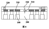
図8及び図9を参照されたい。スルーホール層320は、第1の配線層310の表面S310上に位置し、絶縁層520に一連のスルーホール320を形成するものであり、スルーホールの数や位置は第1の配線層の各配線に対応しており、図9において実線の斜線で塗りつぶされたパターンが即ちスルーホールであり、各LEDチップからできるだけ引き離されている。ここで、スルーホール層520の材料としては絶縁層510の材料を参考にできる。また、スルーホール層520の厚さT320は、好ましくは100μm以下であり、該スルーホール層の最少ライン幅W2の1~2倍とすることが好ましく、例えば需要に応じて1~1.2倍、1.2~1.5倍とすることができ、本実施例において、該層のスルーホールの直径は該層の最少ライン幅W2であり、該スルーホールの直径は20μm~60μmであるとよい。実施形態によっては、パッケージアセンブリはより薄型構造を有し、この場合にはスルーホール層の厚さが20μm~50μmであるとよく、例えば25μm~30μmとすることができる。このようにすれば、スルーホール層が厚すぎて応力や熱抵抗が過大になることを避けることができ、パッケージ構造体の強度を確保しながらも、パッケージ構造体の総厚さを低く抑えることができ、ひいてはこれが応用される製品の厚さをより薄くすることができるようになる。他の実施形態としては、スルーホール層の厚さは50μm~80μmであってもよく、例えば60μmとすることができ、これによりパッケージアセンブリの厚みを適度に増やし、デバイスの側壁からのピックアップを容易にすることができる。
Please refer to Figures 8 and 9. The through-
図10を参照されたい。第2の配線層330は、スルーホール層320上に位置し、スルーホール層320の各スルーホールを介して第1の配線層310と電気的に接続されている。第3の配線層330の各ライン間の隙間には絶縁層530が充填され、第3の配線層330のLEDチップから離れた表面は露出しており、また絶縁層530の材料は、絶縁層510の材料を参考にして設計することができる。
Please refer to FIG. 10. The
図11を参照されたい。第3の配線層330の回路は、複数のライン331ac、331bd、333ac、333bdと、複数の接続部331a、331b、332a、332b、333c、333d、334a、334dと、を有している。この中で、ラインは同じタイプのLEDチップの同じ極性の電極の接続に用いられ、例えば、ライン331acはPx1とPx3の第1のLEDチップ100-L1の第1の電極111を接続し、ライン333acは、Px1とPx3の第3のLEDチップ100-L3の第1の電極111を接続する。接続部は外部に接続する電極パッドとして用いられて電源と接続する。好ましい実施形態では、接続部に対応するエリアにパッドを作成する上、パッド以外のエリアをインク、もしくはエポキシ樹脂もしくは他の絶縁材料で覆うことにより、第2の配線層330のラインを保護する。1つの好ましい実施形態では、該第2の配線層330の接続部はスルーホール層の各スルーホールを完全にカバーすることで、第2の配線層のスルーホールと接触する面積を増やすと共に、製作する過程においては、スルーホール層と第2の配線層を同一のプロセスで電気伝導材料により作成できるので、電気伝導材料の形成及び研磨するプロセスを省くことにより、コストを節約すると共に、製品の安定性を高めることができる。該第3の配線層330の厚さT330は該第3の配線層の最小ライン幅W3の1~2倍であることが好ましく、そして1.2~1.8倍の範囲内であることが更に好ましい。
Please refer to FIG. 11. The circuit of the
絶縁層510~530としては同一の材料を選択することができ、異なる材料を選択することも可能であり、具体的には、エポキシ樹脂、シリコーン、ポリイミド、ベンゾシクロブテンもしくはPBO(ポリパラフェニレンベンゾビスオキサゾール)を選択できる。同一の材料で作成する場合、該絶縁層510~530は一つの層体500を構成するので、区別しにくい。一部の具体的実施形態では、絶縁層510~530として光が通過しないもしくは通過しにくい材料を選択し、例えば黒色の着色剤が添加されたエポキシ樹脂もしくはシリコーンを選択することにより、LEDチップからの光が配線層から射出して干渉を引き起こす状況を回避もしくは抑えることができる。光が通過しないもしくは通過しにくい材料を絶縁層とする場合、まずは配線層における金属ラインのパターンを形成してから絶縁層を充填し、最後に研磨により配線層における金属ラインの表面を露出させる。他の一部の実施形態では、パッケージ層200として光が通過しないもしくは通過しにくい材料を採用する場合、絶縁層510~530は部分的もしくは全体的に光透過性材料を採用することができ、これにより絶縁層の透過率がパッケージ層200の透過率より高くなる。該光透過層としては例えばカーボン粉末や染料などの着色剤が添加されていない材料もしくは光吸収材料、を使用する必要はなく、例えばシリコーンやエポキシ樹脂が好ましく、特に、マイクロメートルレベルの粒子(通常では粒子の直径が1マイクロメートル以上の粒子を指し、例えばカーボン粉末粒子)が含まれていないので、着色剤の添加による不均一や界面の欠陥による信頼性の低下(例えば絶縁性能の低下)の可能性を回避し、絶縁層の配線層に対するカバーの信頼性を確保できる。他の一部の実施形態では、感光性材料により硬化されて絶縁層を形成することにより、制作の工程数を簡単化すると共に、チップ周辺及び電極面の非金属部分が光吸収材料からなるパッケージ層200により覆われるので、チップの側面における光の干渉を回避できる。
The insulating layers 510-530 can be made of the same material or different materials, specifically, epoxy resin, silicone, polyimide, benzocyclobutene, or PBO (polyparaphenylene benzobisoxazole). When made of the same material, the insulating layers 510-530 constitute one
図12と図13を参照されたい。図12には3層の配線層の接続関係が示されており、図13は該4個一体式の発光ユニットの等価回路図である。該4個一体式発光ユニットは接続部331a、331b、332a、332b、333c、333d、334a、334dとの8つの接続部から出力し、その中で第1のLEDチップ100-L1の第1の電極は接続部331a、331bから出力し、第2のLEDチップ100-L2の第1の電極は接続部332a、332bから出力し、第3のLEDチップ100-L2の第1の電極は接続部333c、333dから出力し、接続部334aと334dは共有電極として、それぞれPX1~PX4のすべてのLEDチップの第2の電極112に接続している。
Please refer to Figures 12 and 13. Figure 12 shows the connection relationship of the three wiring layers, and Figure 13 is an equivalent circuit diagram of the four-piece integrated light-emitting unit. The four-piece integrated light-emitting unit outputs from eight connection parts, namely,
この実施形態において、まずはLEDチップの配置に対し、すべてのPxにおけるLEDチップを「一」の字に沿って配列し、具体的には、すべての発光ユニットの各LEDチップを第1の方向に沿って一列に配列し、すべてのLEDチップの第1、第2の電極を第2の方向に沿って並列に配列し、そして第1の方向と第2の方向は基本的に直交するので、隣接する2列のLEDチップの電極の極性は相反する。第1の配線層310において、左右に隣接するPxのLEDチップの共有電極は1つの共有電極として接続するようになり、上下に隣接する2つのPxの第2のLEDチップ100-L2(3つのチップの中間に位置する)は並列接続し(すなわち、Px1とPx3の第2のLEDチップの第1の電極は並列接続、Px1とPx4の第2のLEDチップの第1の電極は並列接続)、Px1~Px4の第1のLEDチップ100-L1、第3のLEDチップ100-L3はそれぞれ個別にワイヤリングすることにより、該4個一体式の発光ユニットの電極端子を10個に減らし、第2の配線層では、上下に隣接する2つのPxの第1、第2のLEDチップはそれぞれ更にラインにより並列(すなわち、Px1とPx3の第1のLEDチップの第1の電極は並列接続して1つの電極端子331aを形成し、Px2とPx4の第1のLEDチップの第1の電極は並列接続して1つの電極端子331bを形成し、Px1のPx3の第3のLEDチップの第1の電極は並列接続して1つの電極端子334cを形成し、Px2とPx4の第3のLEDチップの第1の電極は並列接続して1つの電極端子334dを形成する)、となって合わせて8つの電極端子(即ち8個の接続部)を出力することにより、該パッケージアセンブリの電極パッドの数を効果的に減らして貼り付けが便利になる。
In this embodiment, first, the LED chips in all Px are arranged along the shape of the character "一"; specifically, the LED chips in all light-emitting units are arranged in a row along the first direction, and the first and second electrodes of all LED chips are arranged in parallel along the second direction; and since the first and second directions are basically perpendicular to each other, the polarities of the electrodes of the LED chips in two adjacent rows are opposite. In the
以上に示される実施形態のパッケージアセンブリは、前記LEDチップを載せるパッケージ基板もしくはフレームを使用せず、該m×nマトリックス配置の発光ユニットは主に絶縁材料層(200、400、500を含む)及び配線層により固定、支持されるようになり、該パッケージアセンブリの厚さTはほぼLEDチップの厚さTAと配線層の厚さTCにより決められる。一部の具体的実施形態では、ミニLEDチップを採用し、チップ厚さTAは40~150μm、多層配線層の厚さTCは20~200μm、そして更に好ましくは前記配線層の厚さTCを50~150μmの間にあるように選択することにより、TとTAは1.4≦T/TA≦10の数式を満足し、これにより厚すぎた回路層による応力の過大及び熱抵抗の過大を回避でき、パッケージの構造的強度を確保すると共に、パッケージ構造全体の厚さを減らすことができる。例えば、1つの実施形態では、LEDチップの厚さTAは約80μm、前記パッケージアセンブリの厚さは120μm~500μm、例えば120~200μmであることができ、この際すべての配線層のサブ層の厚さは10~50μmであることができ、例えば40μmである。例えば、他の1つの実施形態では、該パッケージアセンブリのサイズが比較的に小さい場合(例えば0.4mm×0.4mmもしくはもっと小さいサイズ)、パッケージアセンブリの上表面からピックアップしにくいので、パッケージアセンブリの厚さTを適切に増やすことにより、パッケージアセンブリの側壁の面積を比較に広くしてピックアップ設備がピックアップしやすいようにすることができ、この際、パッケージアセンブリの厚さは150~500μmであることができ、例えば180~360μmであり、LEDチップの厚さ及び/または配線層の厚さを増大させることによりパッケージアセンブリの厚さを増大させることができ、例えばLEDチップの電極の厚さを増やすと共に、すべての配線層の厚さを適切に増やし、この際スルーホール層の厚さは30~80μmが好ましく、他の配線層の厚さは50~100μmが好ましい。一部の具体的な実施形態において、マイクロLEDチップを採用し、チップ厚さTAは5~10μm、多層配線層の厚さTCは20~200μmであり、更に好ましくは前記配線層の厚さTCを50~150μmに選択することにより、前記TとTAは10≦T/TA≦60の数式を満足し、例えばパッケージアセンブリの厚さは50~100μm、もしくは100~200μmになり得る。 The package assembly of the above embodiment does not use a package substrate or frame for carrying the LED chip, and the m×n matrix-arranged light-emitting units are mainly fixed and supported by the insulating material layer (including 200, 400, 500) and the wiring layer, and the thickness T of the package assembly is determined approximately by the thickness T A of the LED chip and the thickness T C of the wiring layer. In some specific embodiments, a mini LED chip is used, and the chip thickness T A is 40-150 μm, the thickness T C of the multi-layer wiring layer is 20-200 μm, and more preferably, the thickness T C of the wiring layer is selected to be between 50-150 μm, so that T and T A satisfy the formula 1.4≦T/T A ≦10, thereby avoiding excessive stress and excessive thermal resistance caused by a too thick circuit layer, ensuring the structural strength of the package, and reducing the thickness of the entire package structure. For example, in one embodiment, the thickness T of the LED chip is about 80 μm, the thickness of the package assembly may be 120 μm to 500 μm, for example 120 to 200 μm, and the thickness of all the wiring sub-layers may be 10 to 50 μm, for example 40 μm. For example, in another embodiment, when the size of the package assembly is relatively small (e.g., 0.4 mm×0.4 mm or smaller), it is difficult to pick up the package assembly from the upper surface. Therefore, by appropriately increasing the thickness T of the package assembly, the area of the sidewall of the package assembly can be made relatively large to make it easier for the pick-up equipment to pick it up. In this case, the thickness of the package assembly can be 150 to 500 μm, for example, 180 to 360 μm. The thickness of the package assembly can be increased by increasing the thickness of the LED chip and/or the thickness of the wiring layer, for example by increasing the thickness of the electrode of the LED chip and appropriately increasing the thickness of all the wiring layers, in which case the thickness of the through-hole layer is preferably 30 to 80 μm and the thickness of the other wiring layers is preferably 50 to 100 μm. In some specific embodiments, a micro LED chip is used, the chip thickness T A is 5-10 μm, the multi-layer wiring layer thickness T C is 20-200 μm, and more preferably the wiring layer thickness T C is selected to be 50-150 μm, so that T and T A satisfy the formula 10≦T/T A ≦60, and the thickness of the package assembly can be, for example, 50-100 μm, or 100-200 μm.
図14~図17に本発明のLEDパッケージアセンブリの他の1つの実施形態が示されている。図14を参照されたい。該パッケージアセンブリは同じくm×nマトリックス配置の複数のピクセルエリアPx1~Px4を有し、図3に示されるパッケージアセンブリとの相違点は、すべてのピクセルエリアのLEDチップの電極の方向がすべて同一であり、これによりチップ配列の効率及び精度を高めるのに有利である。この実施形態において、第1の配線層は第1の配線311a、313cと共有配線314a、314dとを有し、この中で311aは横方向に隣接する2つのピクセルエリアPx1とPx2の第1のLEDチップ100-L1を接続し、313cは横方向に隣接する2つのピクセルエリアPx3とPx4の第3のLEDチップ100-L3を接続し、314aは縦方向に隣接するピクセルエリアPx1とPx4のすべてのLEDチップを共有的に接続し、314dは縦方向に隣接するピクセルエリアPx2とPx3のすべてのLEDチップを共有的に接続する。図15と16を参照されたい。第2の配線層は接続部331a、331c、332b、332c、333b、333c、334a、334dと、ライン331cd、332ab、332cd、333abと、を有し、この中で331cdは横方向に隣接するピクセルエリアPx3とPx4の第1のLEDチップ100-L1を接続し、332abは横方向に隣接するピクセルエリアPx1とPx2の第2のLEDチップ100-L2を接続し、332abは横方向に隣接するピクセルエリアPx1とPx2の第2のLEDチップ100-L2を接続し、333cdは横方向に隣接するピクセルエリアPx3とPx4の第3のLEDチップ100-L3を接続する。図17に4個一体式のパッケージアセンブリの等価回路図が示されており、この中で334aと334dはそれぞれ同一の列に位置する発光ユニットのすべてのLEDチップに縦方向に接続し、331a、331c、332b、332c、333b、333cはそれぞれ同一の行に位置する発光ユニットの同一のタイプのLEDチップに横方向に接続する。
Figures 14 to 17 show another embodiment of the LED package assembly of the present invention. Please refer to Figure 14. This package assembly also has a plurality of pixel areas Px1 to Px4 arranged in an m x n matrix, and the difference from the package assembly shown in Figure 3 is that the directions of the electrodes of the LED chips in all pixel areas are all the same, which is advantageous for improving the efficiency and accuracy of the chip arrangement. In this embodiment, the first wiring layer has
図18に本発明のLEDパッケージアセンブリの更に他の1つの実施形態が示されている。該LEDデバイスは同じく2×2マトリックス配置の4つのピクセルエリアPx1~Px4を有し、すべてのピクセルエリアはそれぞれ1つの発光ユニットに対応し、すべてのピクセルエリアのLEDチップは同じ電極方向に沿って配列されている。図14~17に示されるLEDパッケージアセンブリとの異なる点として、第1の配線層330が有する電気伝導路線314aと314bは、それぞれ同一の列にあるすべてのLEDチップの第2の電極112に接続し、第2の配線層が有する電気伝導路線331a~333a、331b~333b、は、それぞれ同一の行に位置する同じタイプのLEDチップの第1の電極111に接続している。例えば、ライン331aは第1の行の第1のタイプのLEDチップの第1の電極111―L1に接続し、ライン332aは第1の行の第2のタイプのLEDチップの第1の電極111―L2に接続し、ライン331bは第2の行的第1のタイプのLEDチップの第1の電極111―L1に接続する。第1の配線層と第2の配線層とはそれらの間にある絶縁層により仕切られ、且つスルーホール層により電気的に接続されている。第1の配線層と第2の配線層との路線の接続方法は、入れ替えることができる。
Figure 18 shows another embodiment of the LED package assembly of the present invention. The LED device also has four pixel areas Px1 to Px4 arranged in a 2x2 matrix, each of which corresponds to one light-emitting unit, and the LED chips in all of the pixel areas are arranged along the same electrode direction. The difference from the LED package assemblies shown in Figures 14 to 17 is that the electrical
図19に本発明のLEDパッケージアセンブリの更に1つの実施形態が示されている。該LEDデバイスは同じく4つのピクセルエリアPx1~Px4を有し、4×1のマトリックス配置となっている。まず、該LEDパッケージアセンブリは長方形もしくは長方形に類する形状になっているので、ディスプレイデバイスに応用される際の組み込みは簡単である上、配線のデザインにより外接パッドの数を最小にすることができる。具体的には、第1の配線層が有するライン314a~314dは、それぞれ縦方向からピクセルエリアPx1~Px4の各発光ユニットの第2の電極に並列接続して4つの外部接続電極端子を形成し、第2の配線層が有する331a~333aはそれぞれピクセルエリアPx1~Px4における同じの第1、第2と第3のLEDチップに接続して3つの外部接続電極子を形成し、これにより該ピクセルエリアPx1~Px4を1つの4個一体式発光モジュールに形成することができる。
Figure 19 shows another embodiment of the LED package assembly of the present invention. The LED device also has four pixel areas Px1-Px4, arranged in a 4x1 matrix. First, the LED package assembly has a rectangular or rectangular-like shape, which makes it easy to install when applied to a display device, and the number of external pads can be minimized by the wiring design. Specifically, the
この実施形態において、該4個一体式のLEDパッケージアセンブリは発光ユニットの配列方法を変更して4×1のマトリックス配置にすることにより、外部接続パッドの数P=4+aとなり、ここでaは1つの発光ユニットにおけるチップの数である。1つの具体的な実施形態において、すべての発光ユニットは赤色光LEDチップ100-L1と、緑色光LEDチップ100-L2と、青色光LEDチップ100-L3との3個のチップを有するので、必要なパッドの数は僅か7となり、パッドの数を最小化してパッケージアセンブリのサイズを小さくすることができる上、配線にも有利で応用側の貼り付けも便利となり、ショートが発生するリスクをも抑える。 In this embodiment, the four-integrated LED package assembly changes the arrangement of the light-emitting units to a 4x1 matrix arrangement, so that the number of external connection pads P = 4 + a, where a is the number of chips in one light-emitting unit. In one specific embodiment, every light-emitting unit has three chips, a red LED chip 100-L1, a green LED chip 100-L2, and a blue LED chip 100-L3, so that only seven pads are required, minimizing the number of pads and reducing the size of the package assembly, which is also advantageous for wiring and convenient for application side attachment, and reduces the risk of short circuits.
図20~22に本発明のLEDパッケージアセンブリの更にもう1つの実施形態が示されている。図20には該LEDパッケージアセンブリのLEDチップの配列状態及び第1の配線層が示されており、該LEDデバイスは同じく16のピクセルエリアPx1~Px4を有し、4×4のマトリックス配置となっている。該16個一体式のLEDパッケージアセンブリにおいて、各発光ユニット間の間隔D1は0.1~0.5mmが好ましく、例えば0.2~0.5mmであることができる。まずは各発光ユニットの各LEDチップを第1の方向に沿って一列に配置し、すべてのLEDチップの第1、第2の電極を第2の方向に沿って並列に配置し、この中で第1の方向と第2の方向とは基本的に直交し、第1の方向において、同一の列に位置するすべてのLEDチップの第2の電極を並列接続し、第2の方向において、同一の行に位置する同一タイプのLEDチップの第1の電極を並列接続し、更に、隣接する列のLEDチップの第1の電極と第2の電極の位置を相反にすることで、同一の行に位置する同一のLEDチップの第1の電極に対する並列接続がしやすくなり、これにより配線層のラインを単純化することができる。具体的には、第1の配線層が有する共有配線314a~314dは、それぞれ共有的にNX1~NX4の列の発光ユニットのLEDチップの第2の電極に接続し、第1のラインが有する311~313において、311はNX2とNX3の列において同一の行に位置する第1のLEDチップL1の第1の電極を接続し、312はNX2とNX3の列において同一の行に位置する第2のLEDチップL2の第1の電極を接続し、313はNX2とNX3の列において同一の行にある第3のLEDチップL3に位置する第1の電極を接続する。第1のラインは更にライン311a~313aを有し、311a~313aはそれぞれNX1とNX4の行にある第1、第2、第3のLEDチップの第1の電極に接続する。図21にスルーホール層のパターンが示され、この一連のスルーホールにおいて、スルーホール324は第1の配線層の共有配線314a~dに接続し、スルーホール321~323はそれぞれ第1の配線層の第1のラインに接続する。図22に第2の配線層のパターンが示され、第2の配線層はライン331~333と接続部331a~333、334とを有し、この中でライン331は同一の行に位置する第1のLEDチップの第1の電極を並列接続し、ライン332は同一の行(例えばNY1~NY4の行)に位置する第2のLEDチップの第1の電極を並列接続し、ライン333は同一の行に位置する第3のLEDチップの第1の電極を並列接続し、接続部は外部接続端子として、その中の331a~333aはそれぞれライン331~333に接続し、334は324と接続する。1つの好ましい実施形態において、接続部に対応するエリアにパッドを作成する上、パッド以外のエリアをインク、もしくはエポキシ樹脂もしくは他の絶縁材料で覆うことにより、第2の配線層のラインを保護する。
20 to 22 show yet another embodiment of the LED package assembly of the present invention. FIG. 20 shows the arrangement of the LED chips and the first wiring layer of the LED package assembly, and the LED device also has 16 pixel areas Px1 to Px4 in a 4x4 matrix arrangement. In the 16-integrated LED package assembly, the distance D1 between each light-emitting unit is preferably 0.1 to 0.5 mm, and can be, for example, 0.2 to 0.5 mm. First, the LED chips of each light-emitting unit are arranged in a row along a first direction, and the first and second electrodes of all of the LED chips are arranged in parallel along a second direction, wherein the first and second directions are basically perpendicular to each other. In the first direction, the second electrodes of all LED chips located in the same column are connected in parallel, and in the second direction, the first electrodes of LED chips of the same type located in the same row are connected in parallel. Furthermore, by reversing the positions of the first and second electrodes of LED chips in adjacent columns, it becomes easier to connect the first electrodes of the same LED chips located in the same row in parallel, and thus the lines of the wiring layer can be simplified. Specifically, the shared
この実施形態において、LEDチップの配列及び配線層の設計を合理化することにより、配線層のラインの接続を簡単化できる上、製品の信頼性を向上し、更に、配線層の層数(外部接続パッド層を含む)を4層以下にすることにより、製品の厚さの薄型化を確保し、最終製品の薄型化にも寄与する。 In this embodiment, by streamlining the arrangement of the LED chips and the design of the wiring layer, the connection of the lines in the wiring layer can be simplified and the reliability of the product can be improved. Furthermore, by limiting the number of wiring layers (including the external connection pad layer) to four or less, the thickness of the product can be reduced, which also contributes to a thinner final product.
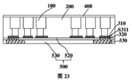
図23は基板を有しないLEDパッケージアセンブリである。パッケージ層200がLEDチップの側壁と第1の配線層310の側壁S311を同時に覆う点において、図2に示されるパッケージアセンブリと異なる。このパッケージ層200としては、光が通過しないもしくは通過しにくい材料が好ましく、例えば透過率30%未満、例えば5~20%が好ましく、更に、該パッケージ層として黒色の材料を選択し、例えば黒色の着色剤が添加されたエポキシ樹脂もしくはシリコーンを選択することが好ましい。絶縁層520と530としては、光が通過するもしくは通過しない材料を選択できる。
Figure 23 shows an LED package assembly without a substrate. It differs from the package assembly shown in Figure 2 in that the
上記のように、本発明のLEDパッケージアセンブリは、該パッケージ層を用いてマトリックス配置のピクセルドットを固定し、且つ、多層配線層を設計して各ピクセルのLEDチップを直列に接続する。従って、本発明にはワイヤボンディングや精密配線を有する回路板を必要としないので、信頼性及びコントラストを向上している。この他、前記LEDチップの電極セットは該回路板に半田付けする必要はなく、チップの半田不良の問題を回避する上、LEDの電子装置の整合性を改善するので、本願発明の目的を確実に達成している。 As described above, the LED package assembly of the present invention uses the package layer to fix the pixel dots in a matrix arrangement, and a multi-layer wiring layer is designed to connect the LED chips of each pixel in series. Therefore, the present invention does not require wire bonding or a circuit board with precision wiring, improving reliability and contrast. In addition, the electrode set of the LED chip does not need to be soldered to the circuit board, which avoids the problem of poor soldering of the chip and improves the integrity of the electronic device of the LED, thereby certainly achieving the objective of the present invention.
図24に本発明の他の1つの実施形態のLEDパッケージアセンブリの構造が示されている。図2に示されるパッケージアセンブリとの相違点については、この実施形態において、配線層における1つもしくは複数の層のリードラインの表面に金属保護層700が形成され、これによりリードラインの金属が拡散することを防止できると共に、腐食や酸化に対抗する効果を発揮することもできる。該保護層の厚さについては20~500nmが好ましく、その材料についてはチタン(Ti)、窒化チタン(TiN)、タングステン(W)、タンタル(Ta)、窒化タンタル(TaN)、モリブデン(Mo)、コバルト(Co)、そしてプラチナ(Pt)などから選択できる。
Figure 24 shows the structure of an LED package assembly according to another embodiment of the present invention. The difference from the package assembly shown in Figure 2 is that in this embodiment, a metal
図25に本発明の更に他の1つの実施形態のLEDパッケージアセンブリの構造が示されている。図14に示されるパッケージアセンブリとの相違点については、この実施形態に示されるパッケージデバイスにおいて、保護層700はリードラインの表面及及び側壁の両方を覆っているところにある。この本実施形態において、該保護層はリードラインを更に良好に保護できる上、配線層と絶縁層500との接着力を向上させることもできる。
Figure 25 shows the structure of an LED package assembly according to yet another embodiment of the present invention. The difference from the package assembly shown in Figure 14 is that in the package device shown in this embodiment, the
以上、本発明の好ましい実施形態を説明したが、本発明はこれらに限定されるものではなく、最も広い解釈の精神および範囲内に含まれる様々な構成として、全ての修飾および均等な構成を包含するものとする。 Although the preferred embodiments of the present invention have been described above, the present invention is not limited to these, and encompasses all modifications and equivalent configurations as various configurations that fall within the spirit and scope of the broadest interpretation.
Claims (28)
各前記発光ユニットは、いずれも1つの第1のLEDチップと1つの第2のLEDチップと1つの第3のLEDチップとを有し、各LEDチップは、反対する第1の表面と第2の表面と、該第1の表面と第2の表面との間に接続されている側面と、前記第2の表面に形成された第1の電極と第2の電極とからなる電極セットとをそれぞれ有し、且つ、前記第1の表面を光射出面とし、各発光ユニットの各LEDチップは第1の方向に沿って一列に並び、各LEDチップの第1、第2の電極は第2の方向に沿って並列に配置されており、
前記パッケージ層は前記LEDチップの間の隙間に充填されると共に、前記LEDチップの側壁を覆っており、
前記配線層は前記複数のLEDチップの第2の表面に形成され、第3の方向において隣接する2つもしくは複数の発光ユニットの第1のLEDチップの第1の電極同士、第2のLEDチップの第1の電極同士、第3のLEDチップの第1の電極同士を接続することにより、該複数の発光ユニットを電気的に接続して1つの複数個一体式の発光モジュールを形成し、第3の方向は第2の方向と同一であり、
前記配線層は複数層のリードラインを有し、各層のリードラインの最小のライン幅Wと該層の厚さTとの関係はW≦T≦2Wである、ことを特徴とする発光ダイオードパッケージアセンブリ。 The light emitting device includes a plurality of light emitting units arranged in an m×n matrix, where m and n are integers and m×n≧4, a package layer, and a wiring layer;
Each of the light-emitting units has one first LED chip, one second LED chip and one third LED chip, each LED chip has a first surface and a second surface opposite to each other, a side surface connected between the first surface and the second surface, and an electrode set consisting of a first electrode and a second electrode formed on the second surface, and the first surface is a light-emitting surface, the LED chips of each light-emitting unit are aligned in a line along a first direction, and the first and second electrodes of each LED chip are arranged in parallel along the second direction,
the package layer fills gaps between the LED chips and covers sidewalls of the LED chips;
the wiring layer is formed on the second surfaces of the plurality of LED chips, and connects first electrodes of first LED chips , first electrodes of second LED chips , and first electrodes of third LED chips of two or more adjacent light emitting units in a third direction, thereby electrically connecting the plurality of light emitting units to form one integrated light emitting module, the third direction being the same as the second direction;
a wiring layer having a plurality of layers of lead lines, and a relationship between a minimum line width W of the lead line of each layer and a thickness T of the layer is W≦T≦2W.
TB/TA≧1
10≧T/TA≧1.4
120μm≧TA≧50μm
の条件を満たすことを特徴とする請求項1に記載の発光ダイオードパッケージアセンブリ。 If the thickness of the LED chip is defined as TA , the thickness of the package layer is defined as TB , and the thickness of the entire package assembly is defined as T, T, TA , and TB can be expressed as:
TB / TA ≧1
10≧T/T A ≧1.4
120μm≧ TA ≧50μm
2. The light emitting diode package assembly according to claim 1, wherein the above condition is satisfied.
TB/TA≧1
60≧T/TA≧10
10μm≧TA≧5μm
の条件に満たすことを特徴とする請求項1に記載の発光ダイオードパッケージアセンブリ。 If the thickness of the LED chip is defined as TA , the thickness of the package layer is defined as TB , and the thickness of the entire package assembly is defined as T, T, TA , and TB can be expressed as:
TB / TA ≧1
60≧T/T A ≧10
10μm≧ TA ≧5μm
2. The light emitting diode package assembly according to claim 1, wherein the above condition is satisfied.
Applications Claiming Priority (7)
| Application Number | Priority Date | Filing Date | Title |
|---|---|---|---|
| CN201921554474.5 | 2019-09-18 | ||
| CN201921554474.5U CN210403768U (en) | 2019-09-18 | 2019-09-18 | Light emitting diode packaging assembly |
| CN201921554475.X | 2019-09-18 | ||
| CN201921554475.XU CN210403726U (en) | 2019-09-18 | 2019-09-18 | Light Emitting Diode Package |
| CN202020278177.9U CN211743151U (en) | 2020-03-09 | 2020-03-09 | Light Emitting Diode Package |
| CN202020278177.9 | 2020-03-09 | ||
| PCT/CN2020/098502 WO2021051924A1 (en) | 2019-09-18 | 2020-06-28 | Light-emitting diode package assembly |
Publications (2)
| Publication Number | Publication Date |
|---|---|
| JP2022536436A JP2022536436A (en) | 2022-08-17 |
| JP7601771B2 true JP7601771B2 (en) | 2024-12-17 |
Family
ID=74883938
Family Applications (1)
| Application Number | Title | Priority Date | Filing Date |
|---|---|---|---|
| JP2021542363A Active JP7601771B2 (en) | 2019-09-18 | 2020-06-28 | Light Emitting Diode Package Assembly |
Country Status (5)
| Country | Link |
|---|---|
| US (1) | US12230612B2 (en) |
| EP (1) | EP4033547A4 (en) |
| JP (1) | JP7601771B2 (en) |
| KR (1) | KR102694716B1 (en) |
| WO (1) | WO2021051924A1 (en) |
Families Citing this family (9)
| Publication number | Priority date | Publication date | Assignee | Title |
|---|---|---|---|---|
| CN115956299A (en) | 2020-10-23 | 2023-04-11 | 东丽株式会社 | Display device and method for manufacturing display device |
| CN113597256A (en) * | 2021-07-29 | 2021-11-02 | 业成科技(成都)有限公司 | Display module and manufacturing method thereof |
| KR102759226B1 (en) * | 2022-08-01 | 2025-01-23 | 한국광기술원 | Micro LED package and Display having the same |
| DE112021007529T5 (en) * | 2021-12-30 | 2024-02-29 | Hubei San'an Optoelectronics Co., Ltd. | Light-emitting module, method for producing a light-emitting module and display device |
| TWI866601B (en) * | 2022-08-29 | 2024-12-11 | 錼創顯示科技股份有限公司 | Light emitting unit |
| TWI835265B (en) * | 2022-08-29 | 2024-03-11 | 錼創顯示科技股份有限公司 | Light emitting unit and display apparatus |
| CN116885084B (en) * | 2023-09-07 | 2023-12-15 | 元旭半导体科技(无锡)有限公司 | An LED chip with its own packaging substrate and its preparation method |
| KR102895485B1 (en) * | 2024-05-27 | 2025-12-12 | 주식회사 글로벌테크놀로지 | Wide coverage light emitting and driving device package, back light unit and display apparatus |
| DE102024121537A1 (en) * | 2024-07-29 | 2026-01-29 | Starlight Display Corporation | Mini-LED light panel used as a display and filled with reflective colloid to increase light brightness, and its mini-LED display |
Citations (3)
| Publication number | Priority date | Publication date | Assignee | Title |
|---|---|---|---|---|
| JP2010171170A (en) | 2009-01-22 | 2010-08-05 | Hitachi Cable Ltd | Copper circuit wiring board and method for manufacturing the same |
| WO2019066491A1 (en) | 2017-09-29 | 2019-04-04 | 서울반도체 주식회사 | Light emitting device and display device having same |
| CN109952641A (en) | 2019-01-15 | 2019-06-28 | 泉州三安半导体科技有限公司 | Light emitting diode package device and light emitting apparatus |
Family Cites Families (16)
| Publication number | Priority date | Publication date | Assignee | Title |
|---|---|---|---|---|
| JP2009054913A (en) * | 2007-08-29 | 2009-03-12 | Seiko Epson Corp | Illumination device and liquid crystal display device |
| KR101926358B1 (en) * | 2012-02-17 | 2018-12-07 | 삼성전자주식회사 | Semiconductor light emitting device and illumination apparatus |
| CN206558500U (en) * | 2016-09-30 | 2017-10-13 | 深圳市玲涛光电科技有限公司 | Light-emitting component, backlight source module and electronic equipment |
| KR102701861B1 (en) * | 2016-11-15 | 2024-09-04 | 삼성디스플레이 주식회사 | Light emitting device and fabricating method thereof |
| CN109216525B (en) * | 2017-07-04 | 2021-08-10 | 英属开曼群岛商錼创科技股份有限公司 | Light emitting module and display device |
| FR3069378B1 (en) * | 2017-07-21 | 2019-08-23 | Aledia | OPTOELECTRONIC DEVICE |
| CN111048656B (en) * | 2017-09-04 | 2024-06-14 | 首尔半导体株式会社 | Display device and method for manufacturing the same |
| KR102536305B1 (en) * | 2018-01-05 | 2023-05-24 | (주)포인트엔지니어링 | Micro led structure and manufactureing method of the same |
| JP6799627B2 (en) * | 2018-02-26 | 2020-12-16 | 山東捷潤弘光電科技有限公司 | RGB-LED package module and its display |
| CN108807356B (en) * | 2018-06-05 | 2020-10-27 | 深圳市智讯达光电科技有限公司 | Four-in-one mini-LED module, display screen and manufacturing method |
| KR102620829B1 (en) * | 2019-08-27 | 2024-01-03 | 삼성전자주식회사 | Light emitting device package and display apparatus including the same |
| CN210403726U (en) * | 2019-09-18 | 2020-04-24 | 厦门三安光电有限公司 | Light Emitting Diode Package |
| CN210607242U (en) * | 2019-09-18 | 2020-05-22 | 厦门三安光电有限公司 | Light Emitting Diode Package |
| CN210403768U (en) * | 2019-09-18 | 2020-04-24 | 厦门三安光电有限公司 | Light emitting diode packaging assembly |
| CN210403724U (en) * | 2019-09-18 | 2020-04-24 | 厦门三安光电有限公司 | Light emitting diode packaging assembly |
| US11695102B2 (en) * | 2020-06-19 | 2023-07-04 | Creeled, Inc. | Active electrical elements with light-emitting diodes |
-
2020
- 2020-06-28 JP JP2021542363A patent/JP7601771B2/en active Active
- 2020-06-28 EP EP20866760.0A patent/EP4033547A4/en active Pending
- 2020-06-28 KR KR1020217021342A patent/KR102694716B1/en active Active
- 2020-06-28 WO PCT/CN2020/098502 patent/WO2021051924A1/en not_active Ceased
-
2022
- 2022-03-10 US US17/691,638 patent/US12230612B2/en active Active
Patent Citations (3)
| Publication number | Priority date | Publication date | Assignee | Title |
|---|---|---|---|---|
| JP2010171170A (en) | 2009-01-22 | 2010-08-05 | Hitachi Cable Ltd | Copper circuit wiring board and method for manufacturing the same |
| WO2019066491A1 (en) | 2017-09-29 | 2019-04-04 | 서울반도체 주식회사 | Light emitting device and display device having same |
| CN109952641A (en) | 2019-01-15 | 2019-06-28 | 泉州三安半导体科技有限公司 | Light emitting diode package device and light emitting apparatus |
Also Published As
| Publication number | Publication date |
|---|---|
| KR20210096270A (en) | 2021-08-04 |
| US20220199592A1 (en) | 2022-06-23 |
| EP4033547A1 (en) | 2022-07-27 |
| WO2021051924A1 (en) | 2021-03-25 |
| EP4033547A4 (en) | 2023-10-25 |
| US12230612B2 (en) | 2025-02-18 |
| JP2022536436A (en) | 2022-08-17 |
| KR102694716B1 (en) | 2024-08-12 |
Similar Documents
| Publication | Publication Date | Title |
|---|---|---|
| JP7601771B2 (en) | Light Emitting Diode Package Assembly | |
| CN210403726U (en) | Light Emitting Diode Package | |
| CN210403768U (en) | Light emitting diode packaging assembly | |
| US8780023B2 (en) | Pixel chip, display panel, lighting panel, display unit, and lighting unit | |
| KR102605973B1 (en) | Pixel module and display apparatus having thereof | |
| CN210403724U (en) | Light emitting diode packaging assembly | |
| KR102708127B1 (en) | Luminescent package assembly, luminescent module and display screen | |
| CN118263235A (en) | Light-emitting device | |
| US12020630B1 (en) | Stacked structure, display screen, and display apparatus | |
| JP7474770B2 (en) | Light Emitting Diode Package Assembly | |
| US11444228B2 (en) | Light emitting device and display apparatus | |
| CN210607242U (en) | Light Emitting Diode Package | |
| CN210403725U (en) | Light emitting diode packaging assembly | |
| CN111162157A (en) | A LED display module | |
| CN211743151U (en) | Light Emitting Diode Package | |
| US9006968B2 (en) | Mounting substrate and optical unit | |
| CN116364739A (en) | Driver panel and display device | |
| CN222762973U (en) | LED display device array | |
| US20250143055A1 (en) | Light-Emitting Device And Display Apparatus | |
| JP2025179035A (en) | Wide-range light-emitting drive package, backlight unit and display device | |
| WO2024190226A1 (en) | Laminated structure and semiconductor device | |
| JP2024092521A (en) | Light emitting device |
Legal Events
| Date | Code | Title | Description |
|---|---|---|---|
| A621 | Written request for application examination |
Free format text: JAPANESE INTERMEDIATE CODE: A621 Effective date: 20210927 |
|
| A131 | Notification of reasons for refusal |
Free format text: JAPANESE INTERMEDIATE CODE: A131 Effective date: 20221004 |
|
| A521 | Request for written amendment filed |
Free format text: JAPANESE INTERMEDIATE CODE: A523 Effective date: 20221220 |
|
| A131 | Notification of reasons for refusal |
Free format text: JAPANESE INTERMEDIATE CODE: A131 Effective date: 20230207 |
|
| A601 | Written request for extension of time |
Free format text: JAPANESE INTERMEDIATE CODE: A601 Effective date: 20230428 |
|
| A521 | Request for written amendment filed |
Free format text: JAPANESE INTERMEDIATE CODE: A523 Effective date: 20230605 |
|
| A02 | Decision of refusal |
Free format text: JAPANESE INTERMEDIATE CODE: A02 Effective date: 20230801 |
|
| A521 | Request for written amendment filed |
Free format text: JAPANESE INTERMEDIATE CODE: A523 Effective date: 20231107 |
|
| A521 | Request for written amendment filed |
Free format text: JAPANESE INTERMEDIATE CODE: A821 Effective date: 20231107 |
|
| A911 | Transfer to examiner for re-examination before appeal (zenchi) |
Free format text: JAPANESE INTERMEDIATE CODE: A911 Effective date: 20231204 |
|
| A912 | Re-examination (zenchi) completed and case transferred to appeal board |
Free format text: JAPANESE INTERMEDIATE CODE: A912 Effective date: 20231222 |
|
| A521 | Request for written amendment filed |
Free format text: JAPANESE INTERMEDIATE CODE: A523 Effective date: 20241009 |
|
| A61 | First payment of annual fees (during grant procedure) |
Free format text: JAPANESE INTERMEDIATE CODE: A61 Effective date: 20241205 |
|
| R150 | Certificate of patent or registration of utility model |
Ref document number: 7601771 Country of ref document: JP Free format text: JAPANESE INTERMEDIATE CODE: R150 |