JP7594696B2 - Semiconductor Device - Google Patents
Semiconductor Device Download PDFInfo
- Publication number
- JP7594696B2 JP7594696B2 JP2024006507A JP2024006507A JP7594696B2 JP 7594696 B2 JP7594696 B2 JP 7594696B2 JP 2024006507 A JP2024006507 A JP 2024006507A JP 2024006507 A JP2024006507 A JP 2024006507A JP 7594696 B2 JP7594696 B2 JP 7594696B2
- Authority
- JP
- Japan
- Prior art keywords
- transistor
- layer
- conductive layer
- region
- oxide semiconductor
- Prior art date
- Legal status (The legal status is an assumption and is not a legal conclusion. Google has not performed a legal analysis and makes no representation as to the accuracy of the status listed.)
- Active
Links
- 239000004065 semiconductor Substances 0.000 title claims description 278
- 230000006870 function Effects 0.000 claims description 81
- 230000015572 biosynthetic process Effects 0.000 claims description 32
- 229910052710 silicon Inorganic materials 0.000 claims description 24
- 239000010703 silicon Substances 0.000 claims description 23
- 239000010410 layer Substances 0.000 description 291
- 239000010408 film Substances 0.000 description 96
- 239000013078 crystal Substances 0.000 description 55
- 238000000034 method Methods 0.000 description 45
- 239000011701 zinc Substances 0.000 description 42
- 239000012535 impurity Substances 0.000 description 38
- 239000007789 gas Substances 0.000 description 33
- 229910052760 oxygen Inorganic materials 0.000 description 31
- QVGXLLKOCUKJST-UHFFFAOYSA-N atomic oxygen Chemical group [O] QVGXLLKOCUKJST-UHFFFAOYSA-N 0.000 description 29
- 239000001301 oxygen Substances 0.000 description 29
- 125000004429 atom Chemical group 0.000 description 20
- 238000010586 diagram Methods 0.000 description 20
- 229910052739 hydrogen Inorganic materials 0.000 description 20
- 239000001257 hydrogen Substances 0.000 description 20
- 239000000758 substrate Substances 0.000 description 20
- XUIMIQQOPSSXEZ-UHFFFAOYSA-N Silicon Chemical compound [Si] XUIMIQQOPSSXEZ-UHFFFAOYSA-N 0.000 description 19
- 229910052751 metal Inorganic materials 0.000 description 17
- 230000008569 process Effects 0.000 description 17
- IJGRMHOSHXDMSA-UHFFFAOYSA-N Atomic nitrogen Chemical compound N#N IJGRMHOSHXDMSA-UHFFFAOYSA-N 0.000 description 14
- 230000000694 effects Effects 0.000 description 14
- VYPSYNLAJGMNEJ-UHFFFAOYSA-N Silicium dioxide Chemical compound O=[Si]=O VYPSYNLAJGMNEJ-UHFFFAOYSA-N 0.000 description 13
- 239000000463 material Substances 0.000 description 12
- 239000010949 copper Substances 0.000 description 11
- 229910000449 hafnium oxide Inorganic materials 0.000 description 11
- WIHZLLGSGQNAGK-UHFFFAOYSA-N hafnium(4+);oxygen(2-) Chemical compound [O-2].[O-2].[Hf+4] WIHZLLGSGQNAGK-UHFFFAOYSA-N 0.000 description 11
- 238000002173 high-resolution transmission electron microscopy Methods 0.000 description 11
- 239000000203 mixture Substances 0.000 description 11
- 102100030393 G-patch domain and KOW motifs-containing protein Human genes 0.000 description 10
- UFHFLCQGNIYNRP-UHFFFAOYSA-N Hydrogen Chemical compound [H][H] UFHFLCQGNIYNRP-UHFFFAOYSA-N 0.000 description 10
- PXHVJJICTQNCMI-UHFFFAOYSA-N Nickel Chemical compound [Ni] PXHVJJICTQNCMI-UHFFFAOYSA-N 0.000 description 10
- 229910052581 Si3N4 Inorganic materials 0.000 description 10
- 229910045601 alloy Inorganic materials 0.000 description 10
- 239000000956 alloy Substances 0.000 description 10
- 150000002431 hydrogen Chemical class 0.000 description 10
- 238000012545 processing Methods 0.000 description 10
- HQVNEWCFYHHQES-UHFFFAOYSA-N silicon nitride Chemical compound N12[Si]34N5[Si]62N3[Si]51N64 HQVNEWCFYHHQES-UHFFFAOYSA-N 0.000 description 10
- 229910052782 aluminium Inorganic materials 0.000 description 9
- XAGFODPZIPBFFR-UHFFFAOYSA-N aluminium Chemical compound [Al] XAGFODPZIPBFFR-UHFFFAOYSA-N 0.000 description 9
- 238000004458 analytical method Methods 0.000 description 9
- 230000007547 defect Effects 0.000 description 9
- 238000004519 manufacturing process Methods 0.000 description 9
- 239000002184 metal Substances 0.000 description 9
- 230000004048 modification Effects 0.000 description 9
- 238000012986 modification Methods 0.000 description 9
- TWNQGVIAIRXVLR-UHFFFAOYSA-N oxo(oxoalumanyloxy)alumane Chemical compound O=[Al]O[Al]=O TWNQGVIAIRXVLR-UHFFFAOYSA-N 0.000 description 9
- 229910052721 tungsten Inorganic materials 0.000 description 9
- 239000010937 tungsten Substances 0.000 description 9
- 238000005520 cutting process Methods 0.000 description 8
- AMWRITDGCCNYAT-UHFFFAOYSA-L hydroxy(oxo)manganese;manganese Chemical compound [Mn].O[Mn]=O.O[Mn]=O AMWRITDGCCNYAT-UHFFFAOYSA-L 0.000 description 8
- MRELNEQAGSRDBK-UHFFFAOYSA-N lanthanum(3+);oxygen(2-) Chemical compound [O-2].[O-2].[O-2].[La+3].[La+3] MRELNEQAGSRDBK-UHFFFAOYSA-N 0.000 description 8
- PLDDOISOJJCEMH-UHFFFAOYSA-N neodymium(3+);oxygen(2-) Chemical compound [O-2].[O-2].[O-2].[Nd+3].[Nd+3] PLDDOISOJJCEMH-UHFFFAOYSA-N 0.000 description 8
- 229910052814 silicon oxide Inorganic materials 0.000 description 8
- 239000002356 single layer Substances 0.000 description 8
- 239000010936 titanium Substances 0.000 description 8
- WFKWXMTUELFFGS-UHFFFAOYSA-N tungsten Chemical compound [W] WFKWXMTUELFFGS-UHFFFAOYSA-N 0.000 description 8
- 229910017566 Cu-Mn Inorganic materials 0.000 description 7
- 229910017871 Cu—Mn Inorganic materials 0.000 description 7
- 238000004891 communication Methods 0.000 description 7
- 239000004020 conductor Substances 0.000 description 7
- 239000002159 nanocrystal Substances 0.000 description 7
- 229910052757 nitrogen Inorganic materials 0.000 description 7
- 238000005477 sputtering target Methods 0.000 description 7
- XKRFYHLGVUSROY-UHFFFAOYSA-N Argon Chemical compound [Ar] XKRFYHLGVUSROY-UHFFFAOYSA-N 0.000 description 6
- XEEYBQQBJWHFJM-UHFFFAOYSA-N Iron Chemical compound [Fe] XEEYBQQBJWHFJM-UHFFFAOYSA-N 0.000 description 6
- RTAQQCXQSZGOHL-UHFFFAOYSA-N Titanium Chemical compound [Ti] RTAQQCXQSZGOHL-UHFFFAOYSA-N 0.000 description 6
- 230000000903 blocking effect Effects 0.000 description 6
- 238000009792 diffusion process Methods 0.000 description 6
- AJNVQOSZGJRYEI-UHFFFAOYSA-N digallium;oxygen(2-) Chemical compound [O-2].[O-2].[O-2].[Ga+3].[Ga+3] AJNVQOSZGJRYEI-UHFFFAOYSA-N 0.000 description 6
- 230000005684 electric field Effects 0.000 description 6
- 238000002003 electron diffraction Methods 0.000 description 6
- 229910001195 gallium oxide Inorganic materials 0.000 description 6
- 239000011261 inert gas Substances 0.000 description 6
- SIWVEOZUMHYXCS-UHFFFAOYSA-N oxo(oxoyttriooxy)yttrium Chemical compound O=[Y]O[Y]=O SIWVEOZUMHYXCS-UHFFFAOYSA-N 0.000 description 6
- BASFCYQUMIYNBI-UHFFFAOYSA-N platinum Chemical compound [Pt] BASFCYQUMIYNBI-UHFFFAOYSA-N 0.000 description 6
- 239000000523 sample Substances 0.000 description 6
- 239000000126 substance Substances 0.000 description 6
- 229910052719 titanium Inorganic materials 0.000 description 6
- 229910001868 water Inorganic materials 0.000 description 6
- OKTJSMMVPCPJKN-UHFFFAOYSA-N Carbon Chemical compound [C] OKTJSMMVPCPJKN-UHFFFAOYSA-N 0.000 description 5
- 238000002441 X-ray diffraction Methods 0.000 description 5
- 229910052799 carbon Inorganic materials 0.000 description 5
- 238000006243 chemical reaction Methods 0.000 description 5
- 230000007423 decrease Effects 0.000 description 5
- 238000005516 engineering process Methods 0.000 description 5
- 239000010931 gold Substances 0.000 description 5
- 150000004767 nitrides Chemical class 0.000 description 5
- 238000002230 thermal chemical vapour deposition Methods 0.000 description 5
- XLYOFNOQVPJJNP-UHFFFAOYSA-N water Substances O XLYOFNOQVPJJNP-UHFFFAOYSA-N 0.000 description 5
- CURLTUGMZLYLDI-UHFFFAOYSA-N Carbon dioxide Chemical compound O=C=O CURLTUGMZLYLDI-UHFFFAOYSA-N 0.000 description 4
- 230000008859 change Effects 0.000 description 4
- 239000011651 chromium Substances 0.000 description 4
- PMHQVHHXPFUNSP-UHFFFAOYSA-M copper(1+);methylsulfanylmethane;bromide Chemical compound Br[Cu].CSC PMHQVHHXPFUNSP-UHFFFAOYSA-M 0.000 description 4
- YBMRDBCBODYGJE-UHFFFAOYSA-N germanium oxide Inorganic materials O=[Ge]=O YBMRDBCBODYGJE-UHFFFAOYSA-N 0.000 description 4
- 229910052738 indium Inorganic materials 0.000 description 4
- 239000012212 insulator Substances 0.000 description 4
- 229910052746 lanthanum Inorganic materials 0.000 description 4
- CPLXHLVBOLITMK-UHFFFAOYSA-N magnesium oxide Inorganic materials [Mg]=O CPLXHLVBOLITMK-UHFFFAOYSA-N 0.000 description 4
- 239000000395 magnesium oxide Substances 0.000 description 4
- AXZKOIWUVFPNLO-UHFFFAOYSA-N magnesium;oxygen(2-) Chemical compound [O-2].[Mg+2] AXZKOIWUVFPNLO-UHFFFAOYSA-N 0.000 description 4
- 230000014759 maintenance of location Effects 0.000 description 4
- 239000011572 manganese Substances 0.000 description 4
- 229910052759 nickel Inorganic materials 0.000 description 4
- PVADDRMAFCOOPC-UHFFFAOYSA-N oxogermanium Chemical compound [Ge]=O PVADDRMAFCOOPC-UHFFFAOYSA-N 0.000 description 4
- BPUBBGLMJRNUCC-UHFFFAOYSA-N oxygen(2-);tantalum(5+) Chemical compound [O-2].[O-2].[O-2].[O-2].[O-2].[Ta+5].[Ta+5] BPUBBGLMJRNUCC-UHFFFAOYSA-N 0.000 description 4
- RVTZCBVAJQQJTK-UHFFFAOYSA-N oxygen(2-);zirconium(4+) Chemical compound [O-2].[O-2].[Zr+4] RVTZCBVAJQQJTK-UHFFFAOYSA-N 0.000 description 4
- 239000011347 resin Substances 0.000 description 4
- 229920005989 resin Polymers 0.000 description 4
- 229910001936 tantalum oxide Inorganic materials 0.000 description 4
- 229910001928 zirconium oxide Inorganic materials 0.000 description 4
- 229910052684 Cerium Inorganic materials 0.000 description 3
- 101100508840 Daucus carota INV3 gene Proteins 0.000 description 3
- ZOKXTWBITQBERF-UHFFFAOYSA-N Molybdenum Chemical compound [Mo] ZOKXTWBITQBERF-UHFFFAOYSA-N 0.000 description 3
- 229910007541 Zn O Inorganic materials 0.000 description 3
- 229910052786 argon Inorganic materials 0.000 description 3
- 238000005229 chemical vapour deposition Methods 0.000 description 3
- 150000001875 compounds Chemical class 0.000 description 3
- AXAZMDOAUQTMOW-UHFFFAOYSA-N dimethylzinc Chemical compound C[Zn]C AXAZMDOAUQTMOW-UHFFFAOYSA-N 0.000 description 3
- 230000005669 field effect Effects 0.000 description 3
- 230000014509 gene expression Effects 0.000 description 3
- PCHJSUWPFVWCPO-UHFFFAOYSA-N gold Chemical compound [Au] PCHJSUWPFVWCPO-UHFFFAOYSA-N 0.000 description 3
- 229910052737 gold Inorganic materials 0.000 description 3
- 229910052735 hafnium Inorganic materials 0.000 description 3
- VBJZVLUMGGDVMO-UHFFFAOYSA-N hafnium atom Chemical compound [Hf] VBJZVLUMGGDVMO-UHFFFAOYSA-N 0.000 description 3
- 125000005843 halogen group Chemical group 0.000 description 3
- AMGQUBHHOARCQH-UHFFFAOYSA-N indium;oxotin Chemical compound [In].[Sn]=O AMGQUBHHOARCQH-UHFFFAOYSA-N 0.000 description 3
- 229910052750 molybdenum Inorganic materials 0.000 description 3
- 239000011733 molybdenum Substances 0.000 description 3
- 229910021421 monocrystalline silicon Inorganic materials 0.000 description 3
- 230000002093 peripheral effect Effects 0.000 description 3
- 235000012239 silicon dioxide Nutrition 0.000 description 3
- 239000010409 thin film Substances 0.000 description 3
- XCZXGTMEAKBVPV-UHFFFAOYSA-N trimethylgallium Chemical compound C[Ga](C)C XCZXGTMEAKBVPV-UHFFFAOYSA-N 0.000 description 3
- 229910052727 yttrium Inorganic materials 0.000 description 3
- 229910052725 zinc Inorganic materials 0.000 description 3
- 229910052726 zirconium Inorganic materials 0.000 description 3
- VYZAMTAEIAYCRO-UHFFFAOYSA-N Chromium Chemical compound [Cr] VYZAMTAEIAYCRO-UHFFFAOYSA-N 0.000 description 2
- RYGMFSIKBFXOCR-UHFFFAOYSA-N Copper Chemical compound [Cu] RYGMFSIKBFXOCR-UHFFFAOYSA-N 0.000 description 2
- 229910005555 GaZnO Inorganic materials 0.000 description 2
- GYHNNYVSQQEPJS-UHFFFAOYSA-N Gallium Chemical compound [Ga] GYHNNYVSQQEPJS-UHFFFAOYSA-N 0.000 description 2
- PWHULOQIROXLJO-UHFFFAOYSA-N Manganese Chemical compound [Mn] PWHULOQIROXLJO-UHFFFAOYSA-N 0.000 description 2
- KJTLSVCANCCWHF-UHFFFAOYSA-N Ruthenium Chemical compound [Ru] KJTLSVCANCCWHF-UHFFFAOYSA-N 0.000 description 2
- ATJFFYVFTNAWJD-UHFFFAOYSA-N Tin Chemical compound [Sn] ATJFFYVFTNAWJD-UHFFFAOYSA-N 0.000 description 2
- GWEVSGVZZGPLCZ-UHFFFAOYSA-N Titan oxide Chemical compound O=[Ti]=O GWEVSGVZZGPLCZ-UHFFFAOYSA-N 0.000 description 2
- NRTOMJZYCJJWKI-UHFFFAOYSA-N Titanium nitride Chemical compound [Ti]#N NRTOMJZYCJJWKI-UHFFFAOYSA-N 0.000 description 2
- 230000004913 activation Effects 0.000 description 2
- 229910052783 alkali metal Inorganic materials 0.000 description 2
- 150000001340 alkali metals Chemical class 0.000 description 2
- 229910052784 alkaline earth metal Inorganic materials 0.000 description 2
- 150000001342 alkaline earth metals Chemical class 0.000 description 2
- 230000005540 biological transmission Effects 0.000 description 2
- 229910002092 carbon dioxide Inorganic materials 0.000 description 2
- 239000001569 carbon dioxide Substances 0.000 description 2
- 229910052804 chromium Inorganic materials 0.000 description 2
- 229910017052 cobalt Inorganic materials 0.000 description 2
- 239000010941 cobalt Substances 0.000 description 2
- GUTLYIVDDKVIGB-UHFFFAOYSA-N cobalt atom Chemical compound [Co] GUTLYIVDDKVIGB-UHFFFAOYSA-N 0.000 description 2
- 229910052802 copper Inorganic materials 0.000 description 2
- 238000002425 crystallisation Methods 0.000 description 2
- 230000008025 crystallization Effects 0.000 description 2
- 238000003795 desorption Methods 0.000 description 2
- 238000010894 electron beam technology Methods 0.000 description 2
- 239000003822 epoxy resin Substances 0.000 description 2
- 229910052733 gallium Inorganic materials 0.000 description 2
- 229910001385 heavy metal Inorganic materials 0.000 description 2
- APFVFJFRJDLVQX-UHFFFAOYSA-N indium atom Chemical compound [In] APFVFJFRJDLVQX-UHFFFAOYSA-N 0.000 description 2
- 229910003437 indium oxide Inorganic materials 0.000 description 2
- PJXISJQVUVHSOJ-UHFFFAOYSA-N indium(iii) oxide Chemical compound [O-2].[O-2].[O-2].[In+3].[In+3] PJXISJQVUVHSOJ-UHFFFAOYSA-N 0.000 description 2
- 229910052741 iridium Inorganic materials 0.000 description 2
- GKOZUEZYRPOHIO-UHFFFAOYSA-N iridium atom Chemical compound [Ir] GKOZUEZYRPOHIO-UHFFFAOYSA-N 0.000 description 2
- 229910052742 iron Inorganic materials 0.000 description 2
- 230000007257 malfunction Effects 0.000 description 2
- 229910052748 manganese Inorganic materials 0.000 description 2
- 238000000465 moulding Methods 0.000 description 2
- QGLKJKCYBOYXKC-UHFFFAOYSA-N nonaoxidotritungsten Chemical compound O=[W]1(=O)O[W](=O)(=O)O[W](=O)(=O)O1 QGLKJKCYBOYXKC-UHFFFAOYSA-N 0.000 description 2
- 239000007800 oxidant agent Substances 0.000 description 2
- 239000008188 pellet Substances 0.000 description 2
- 230000000737 periodic effect Effects 0.000 description 2
- 229910052697 platinum Inorganic materials 0.000 description 2
- 238000005498 polishing Methods 0.000 description 2
- 229920000647 polyepoxide Polymers 0.000 description 2
- 230000001681 protective effect Effects 0.000 description 2
- 229910052707 ruthenium Inorganic materials 0.000 description 2
- 239000000377 silicon dioxide Substances 0.000 description 2
- 238000004544 sputter deposition Methods 0.000 description 2
- 230000003068 static effect Effects 0.000 description 2
- 229910052712 strontium Inorganic materials 0.000 description 2
- CIOAGBVUUVVLOB-UHFFFAOYSA-N strontium atom Chemical compound [Sr] CIOAGBVUUVVLOB-UHFFFAOYSA-N 0.000 description 2
- 229910052715 tantalum Inorganic materials 0.000 description 2
- GUVRBAGPIYLISA-UHFFFAOYSA-N tantalum atom Chemical compound [Ta] GUVRBAGPIYLISA-UHFFFAOYSA-N 0.000 description 2
- OGIDPMRJRNCKJF-UHFFFAOYSA-N titanium oxide Inorganic materials [Ti]=O OGIDPMRJRNCKJF-UHFFFAOYSA-N 0.000 description 2
- 229910052723 transition metal Inorganic materials 0.000 description 2
- IBEFSUTVZWZJEL-UHFFFAOYSA-N trimethylindium Chemical compound C[In](C)C IBEFSUTVZWZJEL-UHFFFAOYSA-N 0.000 description 2
- 229910001930 tungsten oxide Inorganic materials 0.000 description 2
- 229910001233 yttria-stabilized zirconia Inorganic materials 0.000 description 2
- VWQVUPCCIRVNHF-UHFFFAOYSA-N yttrium atom Chemical compound [Y] VWQVUPCCIRVNHF-UHFFFAOYSA-N 0.000 description 2
- YVTHLONGBIQYBO-UHFFFAOYSA-N zinc indium(3+) oxygen(2-) Chemical compound [O--].[Zn++].[In+3] YVTHLONGBIQYBO-UHFFFAOYSA-N 0.000 description 2
- VZSRBBMJRBPUNF-UHFFFAOYSA-N 2-(2,3-dihydro-1H-inden-2-ylamino)-N-[3-oxo-3-(2,4,6,7-tetrahydrotriazolo[4,5-c]pyridin-5-yl)propyl]pyrimidine-5-carboxamide Chemical compound C1C(CC2=CC=CC=C12)NC1=NC=C(C=N1)C(=O)NCCC(N1CC2=C(CC1)NN=N2)=O VZSRBBMJRBPUNF-UHFFFAOYSA-N 0.000 description 1
- 229920000178 Acrylic resin Polymers 0.000 description 1
- 239000004925 Acrylic resin Substances 0.000 description 1
- 101100462325 Arabidopsis thaliana OSB1 gene Proteins 0.000 description 1
- 101100462329 Arabidopsis thaliana OSB3 gene Proteins 0.000 description 1
- 229910002601 GaN Inorganic materials 0.000 description 1
- 229910005534 GaO2 Inorganic materials 0.000 description 1
- JMASRVWKEDWRBT-UHFFFAOYSA-N Gallium nitride Chemical compound [Ga]#N JMASRVWKEDWRBT-UHFFFAOYSA-N 0.000 description 1
- 229910000914 Mn alloy Inorganic materials 0.000 description 1
- MKYBYDHXWVHEJW-UHFFFAOYSA-N N-[1-oxo-1-(2,4,6,7-tetrahydrotriazolo[4,5-c]pyridin-5-yl)propan-2-yl]-2-[[3-(trifluoromethoxy)phenyl]methylamino]pyrimidine-5-carboxamide Chemical compound O=C(C(C)NC(=O)C=1C=NC(=NC=1)NCC1=CC(=CC=C1)OC(F)(F)F)N1CC2=C(CC1)NN=N2 MKYBYDHXWVHEJW-UHFFFAOYSA-N 0.000 description 1
- NIPNSKYNPDTRPC-UHFFFAOYSA-N N-[2-oxo-2-(2,4,6,7-tetrahydrotriazolo[4,5-c]pyridin-5-yl)ethyl]-2-[[3-(trifluoromethoxy)phenyl]methylamino]pyrimidine-5-carboxamide Chemical compound O=C(CNC(=O)C=1C=NC(=NC=1)NCC1=CC(=CC=C1)OC(F)(F)F)N1CC2=C(CC1)NN=N2 NIPNSKYNPDTRPC-UHFFFAOYSA-N 0.000 description 1
- AFCARXCZXQIEQB-UHFFFAOYSA-N N-[3-oxo-3-(2,4,6,7-tetrahydrotriazolo[4,5-c]pyridin-5-yl)propyl]-2-[[3-(trifluoromethoxy)phenyl]methylamino]pyrimidine-5-carboxamide Chemical compound O=C(CCNC(=O)C=1C=NC(=NC=1)NCC1=CC(=CC=C1)OC(F)(F)F)N1CC2=C(CC1)NN=N2 AFCARXCZXQIEQB-UHFFFAOYSA-N 0.000 description 1
- BKAYIFDRRZZKNF-VIFPVBQESA-N N-acetylcarnosine Chemical compound CC(=O)NCCC(=O)N[C@H](C(O)=O)CC1=CN=CN1 BKAYIFDRRZZKNF-VIFPVBQESA-N 0.000 description 1
- BQCADISMDOOEFD-UHFFFAOYSA-N Silver Chemical compound [Ag] BQCADISMDOOEFD-UHFFFAOYSA-N 0.000 description 1
- 238000003917 TEM image Methods 0.000 description 1
- HCHKCACWOHOZIP-UHFFFAOYSA-N Zinc Chemical compound [Zn] HCHKCACWOHOZIP-UHFFFAOYSA-N 0.000 description 1
- JAWMENYCRQKKJY-UHFFFAOYSA-N [3-(2,4,6,7-tetrahydrotriazolo[4,5-c]pyridin-5-ylmethyl)-1-oxa-2,8-diazaspiro[4.5]dec-2-en-8-yl]-[2-[[3-(trifluoromethoxy)phenyl]methylamino]pyrimidin-5-yl]methanone Chemical compound N1N=NC=2CN(CCC=21)CC1=NOC2(C1)CCN(CC2)C(=O)C=1C=NC(=NC=1)NCC1=CC(=CC=C1)OC(F)(F)F JAWMENYCRQKKJY-UHFFFAOYSA-N 0.000 description 1
- 230000008901 benefit Effects 0.000 description 1
- 230000005587 bubbling Effects 0.000 description 1
- 239000003990 capacitor Substances 0.000 description 1
- 229910052800 carbon group element Inorganic materials 0.000 description 1
- 239000000969 carrier Substances 0.000 description 1
- 239000012159 carrier gas Substances 0.000 description 1
- 229910052681 coesite Inorganic materials 0.000 description 1
- 239000002131 composite material Substances 0.000 description 1
- 238000012937 correction Methods 0.000 description 1
- 229910052906 cristobalite Inorganic materials 0.000 description 1
- 238000000151 deposition Methods 0.000 description 1
- 230000006866 deterioration Effects 0.000 description 1
- HQWPLXHWEZZGKY-UHFFFAOYSA-N diethylzinc Chemical compound CC[Zn]CC HQWPLXHWEZZGKY-UHFFFAOYSA-N 0.000 description 1
- KPUWHANPEXNPJT-UHFFFAOYSA-N disiloxane Chemical class [SiH3]O[SiH3] KPUWHANPEXNPJT-UHFFFAOYSA-N 0.000 description 1
- 239000000428 dust Substances 0.000 description 1
- 238000000605 extraction Methods 0.000 description 1
- 230000002349 favourable effect Effects 0.000 description 1
- 229910052732 germanium Inorganic materials 0.000 description 1
- 238000007689 inspection Methods 0.000 description 1
- 239000011810 insulating material Substances 0.000 description 1
- 239000011229 interlayer Substances 0.000 description 1
- 230000001788 irregular Effects 0.000 description 1
- FZLIPJUXYLNCLC-UHFFFAOYSA-N lanthanum atom Chemical compound [La] FZLIPJUXYLNCLC-UHFFFAOYSA-N 0.000 description 1
- 238000005259 measurement Methods 0.000 description 1
- 238000002844 melting Methods 0.000 description 1
- 239000013081 microcrystal Substances 0.000 description 1
- 230000001151 other effect Effects 0.000 description 1
- 239000005011 phenolic resin Substances 0.000 description 1
- 238000001420 photoelectron spectroscopy Methods 0.000 description 1
- 230000000704 physical effect Effects 0.000 description 1
- 238000005268 plasma chemical vapour deposition Methods 0.000 description 1
- 238000007747 plating Methods 0.000 description 1
- 229920006122 polyamide resin Polymers 0.000 description 1
- 229920001721 polyimide Polymers 0.000 description 1
- 239000009719 polyimide resin Substances 0.000 description 1
- 238000007639 printing Methods 0.000 description 1
- 239000010453 quartz Substances 0.000 description 1
- 239000002994 raw material Substances 0.000 description 1
- 230000009467 reduction Effects 0.000 description 1
- 238000011160 research Methods 0.000 description 1
- 238000001004 secondary ion mass spectrometry Methods 0.000 description 1
- VSZWPYCFIRKVQL-UHFFFAOYSA-N selanylidenegallium;selenium Chemical compound [Se].[Se]=[Ga].[Se]=[Ga] VSZWPYCFIRKVQL-UHFFFAOYSA-N 0.000 description 1
- 238000004098 selected area electron diffraction Methods 0.000 description 1
- 229910052709 silver Inorganic materials 0.000 description 1
- 239000004332 silver Substances 0.000 description 1
- 238000004611 spectroscopical analysis Methods 0.000 description 1
- 229910052682 stishovite Inorganic materials 0.000 description 1
- 238000003860 storage Methods 0.000 description 1
- 238000012916 structural analysis Methods 0.000 description 1
- 230000001360 synchronised effect Effects 0.000 description 1
- MZLGASXMSKOWSE-UHFFFAOYSA-N tantalum nitride Chemical compound [Ta]#N MZLGASXMSKOWSE-UHFFFAOYSA-N 0.000 description 1
- 238000012546 transfer Methods 0.000 description 1
- 229910052905 tridymite Inorganic materials 0.000 description 1
- RGGPNXQUMRMPRA-UHFFFAOYSA-N triethylgallium Chemical compound CC[Ga](CC)CC RGGPNXQUMRMPRA-UHFFFAOYSA-N 0.000 description 1
- -1 tungsten nitride Chemical class 0.000 description 1
- 238000004402 ultra-violet photoelectron spectroscopy Methods 0.000 description 1
- XLOMVQKBTHCTTD-UHFFFAOYSA-N zinc oxide Inorganic materials [Zn]=O XLOMVQKBTHCTTD-UHFFFAOYSA-N 0.000 description 1
- 239000011787 zinc oxide Substances 0.000 description 1
Images




Classifications
-
- H—ELECTRICITY
- H03—ELECTRONIC CIRCUITRY
- H03K—PULSE TECHNIQUE
- H03K19/00—Logic circuits, i.e. having at least two inputs acting on one output; Inverting circuits
- H03K19/0175—Coupling arrangements; Interface arrangements
- H03K19/0185—Coupling arrangements; Interface arrangements using field effect transistors only
- H03K19/018507—Interface arrangements
- H03K19/018521—Interface arrangements of complementary type, e.g. CMOS
-
- H—ELECTRICITY
- H03—ELECTRONIC CIRCUITRY
- H03K—PULSE TECHNIQUE
- H03K19/00—Logic circuits, i.e. having at least two inputs acting on one output; Inverting circuits
- H03K19/02—Logic circuits, i.e. having at least two inputs acting on one output; Inverting circuits using specified components
- H03K19/08—Logic circuits, i.e. having at least two inputs acting on one output; Inverting circuits using specified components using semiconductor devices
- H03K19/094—Logic circuits, i.e. having at least two inputs acting on one output; Inverting circuits using specified components using semiconductor devices using field-effect transistors
- H03K19/0944—Logic circuits, i.e. having at least two inputs acting on one output; Inverting circuits using specified components using semiconductor devices using field-effect transistors using MOSFET or insulated gate field-effect transistors, i.e. IGFET
-
- H—ELECTRICITY
- H03—ELECTRONIC CIRCUITRY
- H03K—PULSE TECHNIQUE
- H03K19/00—Logic circuits, i.e. having at least two inputs acting on one output; Inverting circuits
- H03K19/0008—Arrangements for reducing power consumption
-
- H—ELECTRICITY
- H03—ELECTRONIC CIRCUITRY
- H03K—PULSE TECHNIQUE
- H03K19/00—Logic circuits, i.e. having at least two inputs acting on one output; Inverting circuits
- H03K19/0008—Arrangements for reducing power consumption
- H03K19/0013—Arrangements for reducing power consumption in field effect transistor circuits
-
- H—ELECTRICITY
- H03—ELECTRONIC CIRCUITRY
- H03K—PULSE TECHNIQUE
- H03K19/00—Logic circuits, i.e. having at least two inputs acting on one output; Inverting circuits
- H03K19/0008—Arrangements for reducing power consumption
- H03K19/0016—Arrangements for reducing power consumption by using a control or a clock signal, e.g. in order to apply power supply
-
- H—ELECTRICITY
- H03—ELECTRONIC CIRCUITRY
- H03K—PULSE TECHNIQUE
- H03K19/00—Logic circuits, i.e. having at least two inputs acting on one output; Inverting circuits
- H03K19/02—Logic circuits, i.e. having at least two inputs acting on one output; Inverting circuits using specified components
- H03K19/08—Logic circuits, i.e. having at least two inputs acting on one output; Inverting circuits using specified components using semiconductor devices
- H03K19/094—Logic circuits, i.e. having at least two inputs acting on one output; Inverting circuits using specified components using semiconductor devices using field-effect transistors
- H03K19/096—Synchronous circuits, i.e. using clock signals
-
- H—ELECTRICITY
- H03—ELECTRONIC CIRCUITRY
- H03K—PULSE TECHNIQUE
- H03K3/00—Circuits for generating electric pulses; Monostable, bistable or multistable circuits
- H03K3/01—Details
- H03K3/012—Modifications of generator to improve response time or to decrease power consumption
-
- H—ELECTRICITY
- H10—SEMICONDUCTOR DEVICES; ELECTRIC SOLID-STATE DEVICES NOT OTHERWISE PROVIDED FOR
- H10D—INORGANIC ELECTRIC SEMICONDUCTOR DEVICES
- H10D62/00—Semiconductor bodies, or regions thereof, of devices having potential barriers
- H10D62/40—Crystalline structures
- H10D62/405—Orientations of crystalline planes
-
- H—ELECTRICITY
- H10—SEMICONDUCTOR DEVICES; ELECTRIC SOLID-STATE DEVICES NOT OTHERWISE PROVIDED FOR
- H10D—INORGANIC ELECTRIC SEMICONDUCTOR DEVICES
- H10D62/00—Semiconductor bodies, or regions thereof, of devices having potential barriers
- H10D62/80—Semiconductor bodies, or regions thereof, of devices having potential barriers characterised by the materials
-
- H—ELECTRICITY
- H10—SEMICONDUCTOR DEVICES; ELECTRIC SOLID-STATE DEVICES NOT OTHERWISE PROVIDED FOR
- H10D—INORGANIC ELECTRIC SEMICONDUCTOR DEVICES
- H10D84/00—Integrated devices formed in or on semiconductor substrates that comprise only semiconducting layers, e.g. on Si wafers or on GaAs-on-Si wafers
-
- H—ELECTRICITY
- H10—SEMICONDUCTOR DEVICES; ELECTRIC SOLID-STATE DEVICES NOT OTHERWISE PROVIDED FOR
- H10D—INORGANIC ELECTRIC SEMICONDUCTOR DEVICES
- H10D84/00—Integrated devices formed in or on semiconductor substrates that comprise only semiconducting layers, e.g. on Si wafers or on GaAs-on-Si wafers
- H10D84/01—Manufacture or treatment
- H10D84/02—Manufacture or treatment characterised by using material-based technologies
- H10D84/03—Manufacture or treatment characterised by using material-based technologies using Group IV technology, e.g. silicon technology or silicon-carbide [SiC] technology
- H10D84/038—Manufacture or treatment characterised by using material-based technologies using Group IV technology, e.g. silicon technology or silicon-carbide [SiC] technology using silicon technology, e.g. SiGe
-
- H—ELECTRICITY
- H10—SEMICONDUCTOR DEVICES; ELECTRIC SOLID-STATE DEVICES NOT OTHERWISE PROVIDED FOR
- H10D—INORGANIC ELECTRIC SEMICONDUCTOR DEVICES
- H10D84/00—Integrated devices formed in or on semiconductor substrates that comprise only semiconducting layers, e.g. on Si wafers or on GaAs-on-Si wafers
- H10D84/80—Integrated devices formed in or on semiconductor substrates that comprise only semiconducting layers, e.g. on Si wafers or on GaAs-on-Si wafers characterised by the integration of at least one component covered by groups H10D12/00 or H10D30/00, e.g. integration of IGFETs
- H10D84/811—Combinations of field-effect devices and one or more diodes, capacitors or resistors
-
- H—ELECTRICITY
- H10—SEMICONDUCTOR DEVICES; ELECTRIC SOLID-STATE DEVICES NOT OTHERWISE PROVIDED FOR
- H10D—INORGANIC ELECTRIC SEMICONDUCTOR DEVICES
- H10D86/00—Integrated devices formed in or on insulating or conducting substrates, e.g. formed in silicon-on-insulator [SOI] substrates or on stainless steel or glass substrates
- H10D86/40—Integrated devices formed in or on insulating or conducting substrates, e.g. formed in silicon-on-insulator [SOI] substrates or on stainless steel or glass substrates characterised by multiple TFTs
- H10D86/421—Integrated devices formed in or on insulating or conducting substrates, e.g. formed in silicon-on-insulator [SOI] substrates or on stainless steel or glass substrates characterised by multiple TFTs having a particular composition, shape or crystalline structure of the active layer
- H10D86/423—Integrated devices formed in or on insulating or conducting substrates, e.g. formed in silicon-on-insulator [SOI] substrates or on stainless steel or glass substrates characterised by multiple TFTs having a particular composition, shape or crystalline structure of the active layer comprising semiconductor materials not belonging to the Group IV, e.g. InGaZnO
-
- H—ELECTRICITY
- H10—SEMICONDUCTOR DEVICES; ELECTRIC SOLID-STATE DEVICES NOT OTHERWISE PROVIDED FOR
- H10D—INORGANIC ELECTRIC SEMICONDUCTOR DEVICES
- H10D86/00—Integrated devices formed in or on insulating or conducting substrates, e.g. formed in silicon-on-insulator [SOI] substrates or on stainless steel or glass substrates
- H10D86/40—Integrated devices formed in or on insulating or conducting substrates, e.g. formed in silicon-on-insulator [SOI] substrates or on stainless steel or glass substrates characterised by multiple TFTs
- H10D86/60—Integrated devices formed in or on insulating or conducting substrates, e.g. formed in silicon-on-insulator [SOI] substrates or on stainless steel or glass substrates characterised by multiple TFTs wherein the TFTs are in active matrices
-
- Y—GENERAL TAGGING OF NEW TECHNOLOGICAL DEVELOPMENTS; GENERAL TAGGING OF CROSS-SECTIONAL TECHNOLOGIES SPANNING OVER SEVERAL SECTIONS OF THE IPC; TECHNICAL SUBJECTS COVERED BY FORMER USPC CROSS-REFERENCE ART COLLECTIONS [XRACs] AND DIGESTS
- Y02—TECHNOLOGIES OR APPLICATIONS FOR MITIGATION OR ADAPTATION AGAINST CLIMATE CHANGE
- Y02D—CLIMATE CHANGE MITIGATION TECHNOLOGIES IN INFORMATION AND COMMUNICATION TECHNOLOGIES [ICT], I.E. INFORMATION AND COMMUNICATION TECHNOLOGIES AIMING AT THE REDUCTION OF THEIR OWN ENERGY USE
- Y02D10/00—Energy efficient computing, e.g. low power processors, power management or thermal management
Landscapes
- Engineering & Computer Science (AREA)
- Computer Hardware Design (AREA)
- Physics & Mathematics (AREA)
- Computing Systems (AREA)
- General Engineering & Computer Science (AREA)
- Mathematical Physics (AREA)
- Power Engineering (AREA)
- Metal-Oxide And Bipolar Metal-Oxide Semiconductor Integrated Circuits (AREA)
- Semiconductor Integrated Circuits (AREA)
- Logic Circuits (AREA)
- Thin Film Transistor (AREA)
- Manipulation Of Pulses (AREA)
Description
本発明の一態様は半導体装置およびその駆動方法等に関する。 One aspect of the present invention relates to a semiconductor device and a method for driving the same.
本出願の明細書、図面、及び特許請求の範囲(以下、本明細書等と呼ぶ。)で開示する発
明の一態様は上記の技術分野に限定されない。本発明の一態様は物、方法、または製造方
法に関する。または、本発明の一態様はプロセス、マシン、マニュファクチャ、または組
成物(コンポジション・オブ・マター)に関する。本発明の一態様の技術分野は、半導体
装置、表示装置、発光装置、照明装置、蓄電装置および記憶装置などの装置、同装置の駆
動方法、および、同装置の作製方法を一例として挙げることができる。
An embodiment of the invention disclosed in the specification, drawings, and claims of this application (hereinafter referred to as the present specification, etc.) is not limited to the above technical field. An embodiment of the present invention relates to an object, a method, or a manufacturing method. Alternatively, an embodiment of the present invention relates to a process, a machine, a manufacture, or a composition of matter. Examples of the technical field of an embodiment of the present invention include devices such as a semiconductor device, a display device, a light-emitting device, a lighting device, a power storage device, and a memory device, a driving method of the device, and a manufacturing method of the device.
半導体装置のトランジスタの微細化により、リーク電流により静的消費電力が増加すると
いう問題がある。半導体装置の消費電力削減技術として、動作に不要な回路へのクロック
信号の入力を停止するクロックゲーティング技術と、電源供給を遮断するパワーゲーティ
ング技術が知られている。クロックゲーティングでは、動的消費電力を削減できるが、静
的消費電力を十分に削減できない。
As transistors in semiconductor devices are miniaturized, there is a problem that static power consumption increases due to leakage current. Known power consumption reduction technologies for semiconductor devices include clock gating technology, which stops the input of clock signals to circuits that are not required for operation, and power gating technology, which cuts off the power supply. Clock gating can reduce dynamic power consumption, but cannot sufficiently reduce static power consumption.
一のクロック信号を複数の回路に供給するためクロックツリーが用いられている。例えば
、クロックツリーを構成する論理ゲート回路の電源電位の供給を制御することで、クロッ
クツリーのリーク電流を小さくすることが提案されている(例えば、特許文献1―3参照
)。
A clock tree is used to supply one clock signal to multiple circuits. For example, it has been proposed to reduce the leakage current of the clock tree by controlling the supply of power supply potential to logic gate circuits that constitute the clock tree (see, for example,
半導体領域が酸化物半導体で形成されているトランジスタ(以下、”OSトランジスタ”
と呼ぶ。)が適用されている様々な半導体装置が提案されている。例えば、待機状態でオ
フ状態にされるトランジスタをOSトランジスタとすることで、論理回路の待機電力を低
減することが可能であるとされている(例えば、特許文献4参照)。
A transistor in which a semiconductor region is formed using an oxide semiconductor (hereinafter referred to as an “OS transistor”)
For example, it has been proposed that a transistor that is turned off in a standby state is an OS transistor, thereby making it possible to reduce standby power consumption of a logic circuit (see, for example, Patent Document 4).
本発明の一態様は、新規な半導体装置、または同駆動方法、または、同作製方法を提供す
ることを課題の一とする。例えば、本発明の一態様の課題は、消費電力を低減することが
可能な半導体装置を提供すること、または、面積オーバーヘッドを抑えることが可能な半
導体装置を提供することである。
An object of one embodiment of the present invention is to provide a novel semiconductor device, a driving method thereof, or a manufacturing method thereof. For example, an object of one embodiment of the present invention is to provide a semiconductor device capable of reducing power consumption or a semiconductor device capable of suppressing area overhead.
本明細書等の記載から、列記された課題以外の課題も自ずと明らかとなるものであり、ま
た、本発明の各形態について、これら以外の課題を抽出することが可能である。複数の課
題の記載は、互いの課題の存在を妨げるものではなく、また、本発明の一態様は、これら
の課題の全てを解決する必要はない。
From the description of this specification and the like, problems other than those listed will become apparent, and problems other than these can be extracted for each embodiment of the present invention. The description of multiple problems does not preclude the existence of each problem, and one embodiment of the present invention does not need to solve all of these problems.
本発明の一態様は、出力ノードと、第1、および第2ノードと、第1乃至第3トランジス
タと、を有し、1または複数の第1信号を演算処理して、第2信号を出力ノードから出力
することができる機能を有し、第1ノードには、第1電源電位が入力され、第2ノードに
は、第2電源電位が入力され、第1電源電位は第2電源電位よりも高く、第1トランジス
タはp型トランジスタであり、第2および第3トランジスタはn型トランジスタであり、
第2および第3トランジスタの半導体領域は酸化物半導体層を有し、第1トランジスタ、
第3トランジスタ、第2トランジスタの順に直列に電気的に接続され、第1トランジスタ
のソースは第1ノードに電気的に接続され、第2トランジスタのドレインは出力ノードに
電気的に接続され、第2トランジスタのソースは第2ノードに電気的に接続され、第1、
および第2トランジスタのゲートの電位は1または複数の第1信号により制御され、第3
トランジスタのゲートには第3信号が入力される回路である。
One embodiment of the present invention has an output node, first and second nodes, and first to third transistors, and has a function of performing arithmetic processing on one or a plurality of first signals and outputting a second signal from the output node, a first power supply potential is input to the first node, a second power supply potential is input to the second node, the first power supply potential is higher than the second power supply potential, the first transistor is a p-type transistor, and the second and third transistors are n-type transistors,
The semiconductor regions of the second and third transistors have oxide semiconductor layers.
The third transistor and the second transistor are electrically connected in series in this order, the source of the first transistor is electrically connected to a first node, the drain of the second transistor is electrically connected to an output node, and the source of the second transistor is electrically connected to a second node.
and the potential of the gate of the second transistor is controlled by one or more first signals;
A third signal is input to the gate of the transistor.
上記態様において、第3トランジスタに換えて、p型トランジスタを設けることができる
。また、回路は、否定、否定論理積、否定論理和等の論理演算を行う回路とすることがで
きる。
In the above-described embodiment, a p-type transistor may be provided in place of the third transistor. Also, the circuit may be a circuit that performs logical operations such as negation, NAND, and NOR.
本明細書等において、”第1”、”第2”、”第3”という序数詞は構成要素の混同を避
けるために付す場合があり、その場合は数的に限定するものではなく、また順序を限定す
るものでもない。
In this specification, the ordinal numbers "first,""second," and "third" may be used to avoid confusion of components, and in such cases, they do not limit the number or the order.
本明細書等において、半導体装置とは、半導体特性を利用した装置であり、半導体素子(
トランジスタ、ダイオード等)を含む回路、同回路を有する装置等をいう。また、半導体
特性を利用することで機能しうる装置全般をいう。例えば、集積回路、集積回路を備えた
チップは、半導体装置の一例である。また、記憶装置、表示装置、発光装置、照明装置及
び電子機器等は、それ自体が半導体装置であり、半導体装置を有している場合がある。
In this specification, a semiconductor device is a device that utilizes semiconductor characteristics and is a semiconductor element (
A semiconductor device refers to a circuit including a semiconductor device (such as a transistor or a diode) and a device having such a circuit. It also refers to any device that can function by utilizing semiconductor characteristics. For example, an integrated circuit and a chip including an integrated circuit are examples of a semiconductor device. Furthermore, a memory device, a display device, a light-emitting device, a lighting device, an electronic device, and the like are themselves semiconductor devices and may include a semiconductor device.
トランジスタは、ゲート、ソース、およびドレインと呼ばれる3つのノード(端子)を有
する。ゲートは、トランジスタの導通状態を制御する制御ノードとして機能するノードで
ある。ソースまたはドレインとして機能する一対の入出力ノードは、トランジスタの型及
び各ノード(端子)に与えられる電位の高低によって、一方がソースとなり他方がドレイ
ンとなる。一般的に、n型トランジスタでは、低い電位が与えられるノードがソースと呼
ばれ、高い電位が与えられるノードがドレインと呼ばれる。逆に、p型トランジスタでは
、低い電位が与えられるノードがドレインと呼ばれ、高い電位が与えられるノードがソー
スと呼ばれる。
A transistor has three nodes (terminals) called a gate, a source, and a drain. The gate is a node that functions as a control node that controls the conductive state of the transistor. A pair of input/output nodes that function as a source or a drain will be one source and the other drain depending on the type of transistor and the level of the potential applied to each node (terminal). Generally, in an n-type transistor, the node to which a low potential is applied is called the source, and the node to which a high potential is applied is called the drain. Conversely, in a p-type transistor, the node to which a low potential is applied is called the drain, and the node to which a high potential is applied is called the source.
本明細書では、回路構成やその動作の理解を容易にするため、トランジスタの2つの入出
力ノードの一方をソースに、他方をドレインに限定して説明する場合がある。もちろん、
駆動方法によっては、トランジスタの3つの端子に印加される電位の大小関係が変化し、
ソースとドレインが入れ替わる場合がある。したがって、本発明の一態様において、トラ
ンジスタのソースとドレインの区別は、明細書および図面での記載に限定されるものでは
ない。
In this specification, in order to facilitate understanding of the circuit configuration and its operation, there are cases where the description is limited to one of two input/output nodes of a transistor being the source and the other being the drain.
Depending on the driving method, the magnitude relationship of the potentials applied to the three terminals of the transistor changes.
The source and the drain may be interchanged. Therefore, in one embodiment of the present invention, the distinction between the source and the drain of a transistor is not limited to the description in the specification and drawings.
また、本明細書等において、XとYとが接続されている、と明示的に記載する場合は、X
とYとが電気的に接続されている場合と、XとYとが機能的に接続されている場合と、X
とYとが直接接続されている場合とを含むものとする。したがって、所定の接続関係、例
えば、本明細書等に記載されている接続関係に限定されず、本明細書等に示された接続関
係以外のものも含むものとする。ここで、X、Yは、対象物(例えば、装置、素子、回路
、配線、電極、端子、導電膜、層、など)であるとする。
In addition, in the present specification and the like, when it is explicitly stated that X and Y are connected, X
When X and Y are electrically connected, when X and Y are functionally connected, and when X and Y are electrically connected,
and Y are directly connected. Therefore, it is not limited to a specific connection relationship, for example, a connection relationship described in this specification, but also includes connection relationships other than those shown in this specification. Here, X and Y are objects (for example, a device, an element, a circuit, a wiring, an electrode, a terminal, a conductive film, a layer, etc.).
XとYとが電気的に接続されている接続関係の一例としては、XとYとの電気的な接続を
可能とする素子(例えば、スイッチ、トランジスタ、容量素子、インダクタ、抵抗素子、
ダイオード、表示素子、発光素子、負荷など)が、XとYとの間に1個以上接続されるこ
とが可能である。なお、スイッチは、オンオフが制御される機能を有している。つまり、
スイッチは、導通状態(オン状態)、または、非導通状態(オフ状態)になり、電流を流
すか流さないかを制御する機能を有している。または、スイッチは、電流を流す経路を選
択して切り替える機能を有している。
An example of a connection relationship in which X and Y are electrically connected is an element that enables electrical connection between X and Y (for example, a switch, a transistor, a capacitance element, an inductor, a resistance element,
One or more elements (diode, display element, light-emitting element, load, etc.) can be connected between X and Y. The switch has a function of being controlled to be on and off. That is,
A switch has a function of being in a conductive state (on state) or a non-conductive state (off state) to control whether a current flows or not, or a function of selecting and switching a path through which a current flows.
XとYとが機能的に接続されている場合の一例としては、XとYとの機能的な接続を可能
とする回路(例えば、論理回路(インバータ、NAND回路、NOR回路など)、信号変
換回路(DA変換回路、AD変換回路、ガンマ補正回路など)、電位レベル変換回路(電
源回路(昇圧回路、降圧回路など)、信号の電位レベルを変えるレベルシフタ回路など)
、電圧源、電流源、切り替え回路、増幅回路(信号振幅または電流量などを大きく出来る
回路、オペアンプ、差動増幅回路、ソースフォロワ回路、バッファ回路など)、信号生成
回路、記憶回路、制御回路など)が、XとYとの間に1個以上接続されることが可能であ
る。なお、一例として、XとYとの間に別の回路を挟んでいても、Xから出力された信号
がYへ伝達される場合は、XとYとは機能的に接続されているものとする。
An example of a case where X and Y are functionally connected is a circuit that enables the functional connection between X and Y (for example, a logic circuit (an inverter, a NAND circuit, a NOR circuit, etc.), a signal conversion circuit (a DA conversion circuit, an AD conversion circuit, a gamma correction circuit, etc.), a potential level conversion circuit (a power supply circuit (a step-up circuit, a step-down circuit, etc.), a level shifter circuit that changes the potential level of a signal, etc.)
, a voltage source, a current source, a switching circuit, an amplifier circuit (a circuit that can increase the signal amplitude or the amount of current, an operational amplifier, a differential amplifier circuit, a source follower circuit, a buffer circuit, etc.), a signal generating circuit, a memory circuit, a control circuit, etc.) can be connected between X and Y. As an example, even if another circuit is sandwiched between X and Y, if a signal output from X is transmitted to Y, X and Y are considered to be functionally connected.
なお、XとYとが接続されている、と明示的に記載する場合は、XとYとが電気的に接続
されている場合(つまり、XとYとの間に別の素子又は別の回路を挟んで接続されている
場合)と、XとYとが機能的に接続されている場合(つまり、XとYとの間に別の回路を
挟んで機能的に接続されている場合)と、XとYとが直接接続されている場合(つまり、
XとYとの間に別の素子又は別の回路を挟まずに接続されている場合)とを含むものとす
る。つまり、電気的に接続されている、と明示的に記載する場合は、単に、接続されてい
る、とのみ明示的に記載されている場合と同じであるとする。
In addition, when it is explicitly stated that X and Y are connected, it means that X and Y are electrically connected (i.e., X and Y are connected with another element or another circuit between them), X and Y are functionally connected (i.e., X and Y are functionally connected with another circuit between them), and X and Y are directly connected (i.e.,
This includes cases where X and Y are connected without any other element or circuit between them. In other words, when it is explicitly stated that they are electrically connected, it is the same as when it is explicitly stated that they are simply connected.
なお、例えば、トランジスタのソース(又は第1の端子など)が、Z1を介して(又は介
さず)、Xと電気的に接続され、トランジスタのドレイン(又は第2の端子など)が、Z
2を介して(又は介さず)、Yと電気的に接続されている場合や、トランジスタのソース
(又は第1の端子など)が、Z1の一部と直接的に接続され、Z1の別の一部がXと直接
的に接続され、トランジスタのドレイン(又は第2の端子など)が、Z2の一部と直接的
に接続され、Z2の別の一部がYと直接的に接続されている場合では、以下のように表現
することが出来る。
For example, the source (or the first terminal, etc.) of the transistor is electrically connected to X through (or without) Z1, and the drain (or the second terminal, etc.) of the transistor is electrically connected to Z
In the case where a transistor is electrically connected to Y through (or without) Z1, or where a source (or a first terminal, etc.) of the transistor is directly connected to a part of Z1, another part of Z1 is directly connected to X, and a drain (or a second terminal, etc.) of the transistor is directly connected to a part of Z2, and another part of Z2 is directly connected to Y, the above can be expressed as follows:
例えば、「XとYとトランジスタのソース(又は第1の端子など)とドレイン(又は第2
の端子など)とは、互いに電気的に接続されており、X、トランジスタのソース(又は第
1の端子など)、トランジスタのドレイン(又は第2の端子など)、Yの順序で電気的に
接続されている。」と表現することができる。または、「トランジスタのソース(又は第
1の端子など)は、Xと電気的に接続され、トランジスタのドレイン(又は第2の端子な
ど)はYと電気的に接続され、X、トランジスタのソース(又は第1の端子など)、トラ
ンジスタのドレイン(又は第2の端子など)、Yは、この順序で電気的に接続されている
」と表現することができる。または、「Xは、トランジスタのソース(又は第1の端子な
ど)とドレイン(又は第2の端子など)とを介して、Yと電気的に接続され、X、トラン
ジスタのソース(又は第1の端子など)、トランジスタのドレイン(又は第2の端子など
)、Yは、この接続順序で設けられている」と表現することができる。これらの例と同様
な表現方法を用いて、回路構成における接続の順序について規定することにより、トラン
ジスタのソース(又は第1の端子など)と、ドレイン(又は第2の端子など)とを、区別
して、技術的範囲を決定することができる。なお、これらの表現方法は、一例であり、こ
れらの表現方法に限定されない。ここで、X、Y、Z1、Z2は、対象物(例えば、装置
、素子、回路、配線、電極、端子、導電膜、層、など)であるとする。
For example, "X and Y and the source (or first terminal, etc.) and drain (or second terminal, etc.) of a transistor"
The transistor terminals (e.g., terminals) are electrically connected to each other, and are electrically connected in the order of X, the source (or first terminal, etc.) of the transistor, the drain (or second terminal, etc.) of the transistor, and Y. " Alternatively, it can be expressed as "The source (or first terminal, etc.) of the transistor is electrically connected to X, the drain (or second terminal, etc.) of the transistor is electrically connected to Y, and X, the source (or first terminal, etc.) of the transistor, the drain (or second terminal, etc.) of the transistor, and Y are electrically connected in this order." Alternatively, it can be expressed as "X is electrically connected to Y through the source (or first terminal, etc.) and drain (or second terminal, etc.) of the transistor, and X, the source (or first terminal, etc.) of the transistor, the drain (or second terminal, etc.) of the transistor, and Y are provided in this connection order." By using expressions similar to these examples to define the order of connections in a circuit configuration, the source (or first terminal, etc.) and the drain (or second terminal, etc.) of a transistor can be distinguished to determine the technical scope. Note that these expressions are merely examples, and the present invention is not limited to these expressions. Here, X, Y, Z1, and Z2 are objects (e.g., a device, an element, a circuit, a wiring, an electrode, a terminal, a conductive film, a layer, etc.).
本明細書等において、能動素子(例えば、トランジスタ、ダイオードなど)、受動素子(
例えば、容量素子、抵抗素子など)などが有するすべての端子について、その接続先を特
定しなくても、当業者であれば、発明の一態様を構成することは可能な場合がある。つま
り、接続先を特定しなくても、発明の一態様が明確であると言える。そして、接続先が特
定された内容が、本明細書等に記載されている場合、接続先を特定しない発明の一態様が
、本明細書等に記載されていると判断することが可能な場合がある。特に、端子の接続先
が複数のケース考えられる場合には、その端子の接続先を特定の箇所に限定する必要はな
い。したがって、能動素子(トランジスタ、ダイオードなど)、受動素子(容量素子、抵
抗素子など)などが有する一部の端子についてのみ、その接続先を特定することによって
、発明の一態様を構成することが可能な場合がある。
In this specification, the term "active element" refers to an active element (e.g., a transistor, a diode, etc.), a passive element (
For example, even if the connection destinations of all terminals of active elements (e.g., capacitance elements, resistance elements, etc.) are not specified, a person skilled in the art may be able to configure an embodiment of the invention. In other words, an embodiment of the invention can be said to be clear even if the connection destinations are not specified. When the contents in which the connection destinations are specified are described in this specification, etc., it may be possible to determine that an embodiment of the invention in which the connection destinations are not specified is described in this specification. In particular, when there are multiple possible cases in which the connection destinations of a terminal are to be multiple, it is not necessary to limit the connection destination of the terminal to a specific location. Therefore, it may be possible to configure an embodiment of the invention by specifying the connection destinations of only some terminals of active elements (e.g., transistors, diodes, etc.), passive elements (e.g., capacitance elements, resistance elements, etc.).
本明細書等において、ある回路について、少なくとも接続先を特定すれば、当業者であれ
ば、発明を特定することが可能な場合がある。または、ある回路について、少なくとも機
能を特定すれば、当業者であれば、発明を特定することが可能な場合がある。つまり、機
能が特定できれば、発明の態様が明確であると言える。そして、機能が特定された発明の
一態様が、本明細書等に記載されていると判断することが可能な場合がある。したがって
、ある回路について、機能を特定しなくても接続先を特定すれば、発明の一態様が開示さ
れているものであり、発明の一態様を構成することが可能である。または、ある回路につ
いて、接続先を特定しなくても、機能を特定することで、発明の一態様が開示されている
ものであり、発明の一態様を構成することが可能である。
In this specification, etc., if at least the connection destination of a certain circuit is specified, a person skilled in the art may be able to specify the invention. Alternatively, if at least the function of a certain circuit is specified, a person skilled in the art may be able to specify the invention. In other words, if the function can be specified, it can be said that the aspect of the invention is clear. Then, it may be possible to determine that one aspect of the invention in which the function is specified is described in this specification, etc. Therefore, if the connection destination of a certain circuit is specified even if the function is not specified, one aspect of the invention is disclosed and one aspect of the invention can be configured. Alternatively, if the connection destination of a certain circuit is specified even if the connection destination is not specified, one aspect of the invention is disclosed and one aspect of the invention can be configured.
本発明の一態様は、新規な半導体装置、または同駆動方法、または、同作製方法を提供す
ることが可能である。例えば、本発明の一態様により、半導体装置の消費電力を低減する
ことが可能になる、または面積オーバーヘッドを抑えることが可能になる。
According to one embodiment of the present invention, it is possible to provide a novel semiconductor device, a driving method thereof, or a manufacturing method thereof. For example, according to one embodiment of the present invention, it is possible to reduce power consumption of a semiconductor device or suppress area overhead.
これらの効果の記載は、他の効果の存在を妨げるものではない。また、本発明の一態様は
、必ずしも、これらの効果の全てを有する必要はない。また、本発明の一態様はこれらの
効果に限定されるものではない。例えば、場合によって、または、状況に応じて、本発明
の一態様はこれらの効果以外の効果を有する場合もあり、あるいは、これらの効果を有さ
ない場合もある。本発明の一態様について、上記以外の課題、効果、および新規な構成に
ついては、本明細書等の記載から自ずと明らかになるものである。
The description of these effects does not preclude the existence of other effects. Moreover, one embodiment of the present invention does not necessarily have all of these effects. Moreover, one embodiment of the present invention is not limited to these effects. For example, depending on the case or the situation, one embodiment of the present invention may have effects other than these effects, or may not have these effects. Problems, effects, and novel configurations other than those described above regarding one embodiment of the present invention will become apparent from the description in this specification, etc.
図面を用いて、本発明の実施の形態について詳細に説明する。ただし、本発明の一態様は
以下の説明に限定されず、本発明の一態様の趣旨およびその範囲から逸脱することなくそ
の形態および詳細を様々に変更し得ることは、当業者であれば容易に理解される。したが
って、本発明の一態様は、以下に示す実施の形態の記載内容に限定して解釈されるもので
はない。
The embodiments of the present invention will be described in detail with reference to the drawings. However, one aspect of the present invention is not limited to the following description, and it is easily understood by those skilled in the art that the form and details of one aspect of the present invention can be modified in various ways without departing from the spirit and scope of the present invention. Therefore, one aspect of the present invention should not be interpreted as being limited to the description of the embodiments shown below.
以下に、いくつかの実施の形態を示す。1つの実施の形態に記載された構成は他の実施の
形態に記載された構成と適宜組み合わせることが可能である。また、1つの実施の形態に
いくつかの構成例が示される場合は、互い構成例を適宜組み合わせることが可能である。
Several embodiments are described below. A configuration described in one embodiment can be appropriately combined with a configuration described in another embodiment. In addition, when several configuration examples are shown in one embodiment, the configuration examples can be appropriately combined with each other.
また、発明の実施の形態の説明に用いられる図面において、同一部分または同様な機能を
有する部分には同一の符号を付し、その繰り返しの説明は省略する場合がある。また、本
明細書において、例えば、クロック信号CLKを、単に信号CLK、CLK等と省略して
記載する場合がある。これは、他の構成要素(例えば、信号、電圧、電位、回路、素子、
電極、配線等)についても同様である。
In addition, in the drawings used to explain the embodiments of the invention, the same parts or parts having similar functions are given the same reference numerals, and repeated explanations thereof may be omitted. In addition, in this specification, for example, a clock signal CLK may be simply referred to as a signal CLK, CLK, etc. This is because the clock signal CLK may be abbreviated to other components (for example, signals, voltages, potentials, circuits, elements,
The same applies to other components (electrodes, wiring, etc.).
なお、本明細書等では、信号が高レベル電位であることを”H”と記載し、低レベル電位
であることを”L”と記載する場合がある。
In this specification and the like, a high level potential of a signal may be referred to as "H" and a low level potential may be referred to as "L".
(実施の形態1)
<<半導体装置の構成例>>
パワーゲーティングが可能な半導体装置について説明する。図1、図2は半導体装置の構
成例を説明するための図である。図1、図2に示す半導体装置は、出力ノードへの高電源
電位VDDの供給を遮断できるスイッチを設けることで、待機状態でのリーク電流を削減
することを可能にしたものである。本明細書では、回路への電源電位の供給を制御するこ
とができる機能を有するスイッチを”パワースイッチ”と呼ぶ。
(Embodiment 1)
<<Configuration example of semiconductor device>>
A semiconductor device capable of power gating will be described. Figures 1 and 2 are diagrams for explaining a configuration example of the semiconductor device. The semiconductor device shown in Figures 1 and 2 is provided with a switch that can cut off the supply of a high power supply potential VDD to an output node, thereby making it possible to reduce leakage current in a standby state. In this specification, a switch having a function of controlling the supply of a power supply potential to a circuit is called a "power switch."
<構成例1>
図1Aに示す回路21には、高電源電位VDDおよび低電源電位VSSが供給される。回
路21は、n型トランジスタおよびp型トランジスタ双方を含むCMOS回路であり、少
なくとも、2つのn型トランジスタ(トランジスタQn1、トランジスタQn2)、およ
び1つのp型トランジスタ(トランジスタQp1)を有する。トランジスタQn2は、回
路21のパワーゲーティングを制御するパワースイッチとして機能することができる。
<Configuration Example 1>
1A is supplied with a high power supply potential VDD and a low power supply potential VSS. The
つまり回路21は、パワースイッチを備えた機能回路である。機能回路には、基本論理演
算を行うことが可能な論理ゲート回路を適用することができる。例えば、回路21に適用
される論理ゲート回路には、インバータ回路(NOTゲート回路)、NANDゲート回路
、NORゲート回路、ANDゲート回路、ORゲート回路、およびバッファ回路などがあ
る。
That is, the
図1Aの例では、回路21は、1入力1出力の論理回路として機能することが可能であり
、入力ノードa1から入力される信号A1を処理して、信号B1を出力ノードb1から出
力する。回路21の入力ノードの数は1よりも多くてもよい。回路21はノードp1、ノ
ードp2を有する。ノードp1にはVDDが入力され、ノードp2にはVSSが入力され
る。
1A, the
トランジスタQp1とトランジスタQn1は、回路21の論理回路部を構成するトランジ
スタであり、トランジスタQp1とトランジスタQn1は互いのドレインが電気的に接続
され、かつ、これらのドレインは出力ノードb1に電気的に接続されている。トランジス
タQn1のソースはノードp2に電気的に接続されている。トランジスタQn1のソース
とノードp2の電気的な接続は、直接的でもよいし、トランジスタなどの他の素子を介す
る間接的な接続でもよい。トランジスタQp1およびトランジスタQn1のゲートの電位
は信号A1により決定され、トランジスタQp1およびトランジスタQn1のゲートの電
位に応じて、ノードb1の論理レベルが決定される。
The transistors Qp1 and Qn1 are transistors that constitute the logic circuit section of the
トランジスタQn2は、トランジスタQp1のソースへのVDDの供給を遮断できるよう
に設けられている。トランジスタQn2はトランジスタQp1のソースへのVDDの供給
を制御するパワースイッチとして機能することができる。トランジスタQn2のドレイン
はノードp1と電気的に接続されている。トランジスタQn2のソースはトランジスタQ
p1のソースと電気的に接続されている。トランジスタQn1のソースとトランジスタQ
p1のソース間の電気的な接続は、直接的でもよいし、トランジスタなどの他の素子を介
する間接的な接続でもよい。信号SLPはトランジスタQn2の導通状態を制御する制御
信号である。
The transistor Qn2 is provided so as to be able to cut off the supply of VDD to the source of the transistor Qp1. The transistor Qn2 can function as a power switch that controls the supply of VDD to the source of the transistor Qp1. The drain of the transistor Qn2 is electrically connected to the node p1. The source of the transistor Qn2 is connected to the node p2 of the transistor Qp1.
The source of the transistor Qn1 and the source of the transistor Qp1 are electrically connected to each other.
The electrical connection between the sources of p1 may be direct, or may be indirect via another element such as a transistor. A signal SLP is a control signal that controls the conductive state of the transistor Qn2.
また、トランジスタQn2は、VDDを供給するための配線と回路21との電気的な接続
を制御するパワースイッチとして機能させることもできる。
The transistor Qn2 can also function as a power switch that controls the electrical connection between the wiring for supplying VDD and the
回路21が通常動作しているときは、信号SLPを高レベル電位(”H”)にしてトラン
ジスタQn2を導通状態にする。回路21では論理演算が実行される。回路21を待機状
態にするときは、信号SLPを低レベル電位(”L”)にしてトランジスタQn2を非導
通状態にする。トランジスタQp1のゲートが”H”であり、トランジスタQp1が非導
通状態であるときに待機状態になる場合、トランジスタQp1のソースへの高レベル電位
の供給が遮断されているので、トランジスタQp1のソースードレイン間のリーク電流を
無くすまたは削減することができる。
When
トランジスタQn1のゲートが”L”のときに回路21が待機状態になる場合、トランジ
スタQn1のソースードレイン間のリーク電流を無くすまたは低減するため、トランジス
タQn1には、オフ電流が極めて小さなトランジスタが用いられる。オフ電流とは、非導
通状態でのドレイン電流のことをいう。
When the gate of the transistor Qn1 is at "L" and the
トランジスタのオフ電流を下げるには、例えば、半導体領域をエネルギーキャップが広い
半導体で形成すればよい。この場合、半導体のエネルギーギャップは、2.5eV以上、
または2.7eV以上、または3eV以上であることが好ましい。このような半導体とし
て酸化物半導体が挙げられる。例えば、チャネル幅で規格化したOSトランジスタのオフ
電流は、ソースードレイン間電圧が10V、室温(25℃程度)の状態で10×10-2
1A/μm(10ゼプトA/μm)以下とすることが可能である。
In order to reduce the off-state current of a transistor, for example, a semiconductor region may be formed using a semiconductor having a wide energy gap.
An example of such a semiconductor is an oxide semiconductor. For example, the off-state current of an OS transistor normalized by the channel width is 10×10 −2 or more when the source-drain voltage is 10 V and the temperature is at room temperature (about 25° C.).
It is possible to achieve a value of 1 A/μm (10 zeptoA/μm) or less.
我々の研究において、現状、半導体領域が酸化物半導体で形成されたOSトランジスタで
、Siトランジスタと共に同一の回路に組み込むことができる実用的な特性を有するもの
は、n型トランジスタのみである。そこで、トランジスタQn1およびトランジスタQn
2をOSトランジスタとする。また、回路21のリーク電流をより効果的に低減するには
、回路21が有する全てのn型トランジスタがOSトランジスタであることが好ましい。
回路21が有するOSトランジスタのリーク電流は85℃にて1×10-15A以下、ま
たは1×10-18A以下、または1×10-21A以下であることが好ましい。
In our research, at present, among OS transistors whose semiconductor regions are formed using an oxide semiconductor, only n-channel transistors have practical characteristics that allow them to be incorporated into the same circuit together with Si transistors.
In order to more effectively reduce leakage current of the
The leakage current of the OS transistor included in the
回路21が有するp型トランジスタの半導体領域の材料に特段の制約はない。例えば、回
路21が有するp型トランジスタの半導体領域は、Si、Ge、C等の第14族元素を1
つまたは複数含む半導体で形成されていてもよいし、窒化ガリウムなどの窒化物半導体で
形成されていてもよい。代表的には、p型トランジスタは、シリコンでなる半導体領域を
有するSiトランジスタとすればよい。
There is no particular restriction on the material of the semiconductor region of the p-type transistor in the
The p-type transistor may be formed of a semiconductor containing one or more of these elements, or may be formed of a nitride semiconductor such as gallium nitride. Typically, the p-type transistor may be a Si transistor having a semiconductor region made of silicon.
トランジスタQn2が導通状態であるとき、トランジスタQn2のしきい値電圧の影響に
より、トランジスタQp1のソースの状態が、”H”と”L”の中間状態となる場合は、
信号SLPの高レベルの電位をVDDよりも高くすることが好ましい。これにより、回路
21が通常動作モードである期間、トランジスタQp1のソースを確実に”H”にするこ
とができるため、回路21の誤動作を防止できる。
When the transistor Qn2 is in a conductive state, if the state of the source of the transistor Qp1 becomes an intermediate state between “H” and “L” due to the influence of the threshold voltage of the transistor Qn2,
It is preferable that the high-level potential of the signal SLP is set higher than VDD, so that the source of the transistor Qp1 can be reliably set to “H” while the
<構成例2>
図1Bに示す回路22は、回路21の変形例である。パワーゲーティング用のスイッチ回
路として、トランジスタQn2に換えて、トランジスタQn3を設けている。トランジス
タQn3もトランジスタQn2と同様、n型トランジスタであり、かつOSトランジスタ
である。
<Configuration Example 2>
1B is a modification of the
トランジスタQp1のソースはノードp1に電気的に接続されている。トランジスタQp
1のソースとノードp1の電気的な接続は、直接的でもよいし、トランジスタなどの他の
素子を介する間接的な接続でもよい。
The source of the transistor Qp1 is electrically connected to the node p1.
The electrical connection between the source of node p1 and node p1 may be direct, or may be indirect via another element such as a transistor.
トランジスタQn3のゲートには信号SLPが入力される。トランジスタQn3は、トラ
ンジスタQn1のドレインとトランジスタQp1のドレイン間の導通状態を制御するスイ
ッチとして機能する。トランジスタQn3のドレインはトランジスタQp1のドレインと
電気的に接続され、同ソースはトランジスタQn1のドレインと電気的に接続されている
。
A signal SLP is input to the gate of the transistor Qn3. The transistor Qn3 functions as a switch that controls the conduction state between the drain of the transistor Qn1 and the drain of the transistor Qp1. The drain of the transistor Qn3 is electrically connected to the drain of the transistor Qp1, and the source of the transistor Qn3 is electrically connected to the drain of the transistor Qn1.
回路22は、トランジスタQn1のゲートの状態が”H”である時に、待機状態にするこ
とで、回路22の消費電力を効果的に削減できる。トランジスタQn1のゲートが”H”
のときに待機状態になるため、待機状態の間ノードb1の”L”が維持される。そのため
、回路22が通常動作の再開時にノードb1の状態を復帰させるための電力が不要になる
。
The
Since the standby state is entered when the node b1 is turned off, the node b1 is maintained at "L" during the standby state. Therefore, power is not required for restoring the state of the node b1 when the
ノードb1の状態が”H”であるべきときに、トランジスタQn3のしきい値電圧の影響
により、ノードb1の状態が”H”と”L”の中間状態となる場合は、信号SLPの高レ
ベルの電位をVDDよりも高くするとよい。これにより、回路22が通常動作モードのと
き、回路22の出力信号B1が入力される回路の誤動作を防止できる。
When the state of node b1 should be "H", if the threshold voltage of transistor Qn3 causes the state of node b1 to be intermediate between "H" and "L", it is advisable to set the high-level potential of signal SLP higher than VDD. This makes it possible to prevent malfunction of a circuit to which output signal B1 of
<構成例3、4>
図2Aは回路21の変形例である。図2Aに示す回路23は、トランジスタQn2に換え
てp型トランジスタ(トランジスタQp2)が設けられている。図2Bに示す回路24は
回路22の変形例であり、トランジスタQn3に換えてp型トランジスタ(トランジスタ
Qp3)が設けられている。
<Configuration Examples 3 and 4>
Fig. 2A is a modification of the
また、回路22、24には出力ノードb1とトランジスタQp1のドレインとの間にパワ
ースイッチを設けているため、待機状態でトランジスタQp1にゲートリークが生じた場
合でも、出力ノードb1の電位は影響を受けにくい。
Furthermore, since the
OSトランジスタは非導通状態でのリーク電流をほぼゼロとみなすことができるため、O
Sトランジスタが、パワースイッチに適用されている回路21、22の方が、回路23、
24よりも待機状態でのリーク電流をより削減することが可能である。
Since the leakage current of an OS transistor in a non-conducting state can be considered to be almost zero,
The
It is possible to reduce the leakage current in the standby state more than with the conventional MOSFET.
<構成例5>
回路21において、パワースイッチとして機能するトランジスタQn2にバックゲートを
設けてもよい。例えば、トランジスタQn2のゲート(フロントゲート)と独立して、バ
ックゲートの電位を制御できるようにするとよい。また、回路21において、その他のO
Sトランジスタも同様である。OSトランジスタが導通状態と、非導通状態とでバックゲ
ートの電位を異ならせて、導通状態では適切な大きさのドレイン電流が流れ、非導通状態
ではリーク電流を非常に小さくすることが可能となる。なお、導通状態でのドレイン電流
をオン電流と呼ぶ場合がある。
<Configuration Example 5>
In the
The same applies to an S transistor. By making the potential of the backgate of an OS transistor different between the conductive state and the non-conductive state, an appropriate amount of drain current flows in the conductive state and a leakage current can be made very small in the non-conductive state. Note that the drain current in the conductive state may be referred to as an on-current.
回路21の動的消費電力を削減するにはVDDを下げることが効果的である。そのため、
低いVDDでも回路21が所定の処理を実行できるように、OSトランジスタは十分なオ
ン電流特性を備えていることが好ましい。そのようなオン電流特性を持つOSトランジス
タでは、ゲートの電位をVSSにしてもリーク電流が大きくなる場合がある。このような
場合、待機モードでは、バックゲートの電位を制御してOSトランジスタのリーク電流が
小さくなるようにすればよい。また、通常動作モードでは、OSトランジスタのオン電流
が大きくなるようにバックゲートの電位を制御してもよい。以上のことは、回路22-回
路24に含まれるOSトランジスタについても同様である。
In order to reduce the dynamic power consumption of the
It is preferable that the OS transistor has sufficient on-current characteristics so that the
上掲したように、演算処理を行う回路にVDDの遮断を制御するパワースイッチを設ける
ことで、待機状態で非導通状態となるp型トランジスタのリーク電流を削減することがで
きる。また、n型トランジスタにOSトランジスタを適用することで、待機状態で非導通
状態となるn型トランジスタのリーク電流を削減することができる。また、VSSを遮断
するためのパワースイッチを設ける必要がないため、このVSS遮断用のパワースイッチ
の追加による回路面積の増加が抑制されたり、このパワースイッチを制御するため電力が
不要となる。
As described above, by providing a power switch for controlling the cutoff of VDD in a circuit that performs arithmetic processing, the leakage current of a p-type transistor that is in a non-conducting state in a standby state can be reduced. In addition, by applying an OS transistor to an n-type transistor, the leakage current of an n-type transistor that is in a non-conducting state in a standby state can be reduced. In addition, since there is no need to provide a power switch for cutting off VSS, an increase in the circuit area due to the addition of a power switch for cutting off VSS is suppressed, and power for controlling the power switch is not required.
以上述べたように、上掲した構成例では、パワーゲーティング機能を回路に追加すること
による面積オーバーヘッドを抑えつつ、待機状態での電力消費を効果的に削減することが
可能である。
As described above, in the configuration example given above, it is possible to effectively reduce power consumption in the standby state while suppressing area overhead caused by adding a power gating function to the circuit.
<<回路構成例>>
以下、上掲した構成例のより具体的な回路構成を説明する。図3は1入力1出力回路の具
体例であり、インバータ回路が示されている。図4、図5は2入力1出力回路の具体例で
あり、それぞれ、NANDゲート回路、NORゲート回路が示されている。以下では、イ
ンバータ回路、NANDゲート回路およびNORゲート回路を、それぞれ、INV、NA
ND、NORと呼ぶ場合がある。
<<Circuit configuration example>>
More specific circuit configurations of the above-mentioned configuration examples will be described below. Fig. 3 is a specific example of a one-input, one-output circuit, and shows an inverter circuit. Figs. 4 and 5 are specific examples of a two-input, one-output circuit, and show a NAND gate circuit and a NOR gate circuit, respectively. In the following, the inverter circuit, NAND gate circuit, and NOR gate circuit will be referred to as INV, NA, respectively.
Sometimes called ND or NOR.
<インバータ回路>
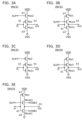
図3Aは回路21の具体例である。図3Aに示すINV31は、p型トランジスタMp1
、n型トランジスタMos1、およびn型トランジスタMos2を有する。トランジスタ
Mos1、Mos2はOSトランジスタである。トランジスタMp1とトランジスタMo
s1により、CMOS型のインバータ回路が構成されている。トランジスタMos2が図
1AのトランジスタQn2に相当するトランジスタである。
<Inverter circuit>
FIG. 3A is a specific example of the
, an n-type transistor Mos1, and an n-type transistor Mos2. The transistors Mos1 and Mos2 are OS transistors.
A CMOS inverter circuit is configured by transistor s1. Transistor Mos2 is a transistor corresponding to transistor Qn2 in FIG.
図3Bは回路22の具体例である。図3Bに示すINV32は、トランジスタMp1、ト
ランジスタMos1、およびトランジスタMos3を有する。トランジスタMp1はp型
であり、トランジスタMos1、Mos3はn型であり、またOSトランジスタである。
トランジスタMos3が図1BのトランジスタQn3に相当するトランジスタである。
3B is a specific example of the
The transistor Mos3 corresponds to the transistor Qn3 in FIG. 1B.
図3Cは回路23の具体例である。図3Cに示すINV33は、トランジスタMp1、ト
ランジスタMp2,およびトランジスタMos1を有する。トランジスタMp2が図2A
のトランジスタQp2に相当するトランジスタである。
3C is a specific example of the
This transistor corresponds to the transistor Qp2.
図3Dは回路24の具体例である。図3Dに示すINV34は、トランジスタMp1、ト
ランジスタMp3、トランジスタMos1を有する。トランジスタMp3が図2Bのトラ
ンジスタQp3に相当するトランジスタである。
Fig. 3D is a specific example of the
図3Eに示すINV35は、上掲の構成例5に対応する回路であり、INV32の変形例
である。トランジスタMos1、Mos3に換えて、バックゲートを有するトランジスタ
Mosb1、Mosb3が設けられている。トランジスタMosb1のバックゲートには
信号OSB1が入力され、トランジスタMosb3のバックゲートには信号OSB3が入
力される。トランジスタMosb1、Mosb3のそれぞれのバックゲートに共通の制御
信号を入力してもよい。
3E is a circuit corresponding to the above-mentioned configuration example 5, and is a modified example of INV32. Transistors Mosb1 and Mosb3 having back gates are provided instead of the transistors Mos1 and Mos3. A signal OSB1 is input to the back gate of the transistor Mosb1, and a signal OSB3 is input to the back gate of the transistor Mosb3. A common control signal may be input to the back gates of the transistors Mosb1 and Mosb3.
<NANDゲート回路>
図4Aは回路21の具体例である。図4Aに示すNAND41は2つの入力ノードa1、
a2を有する。NAND41は、2つのp型トランジスタ(Mp11、Mp12)および
2つのn型トランジスタ(Mos11、Mos12)で構成されるNANDゲート回路に
、トランジスタMos2を追加したものである。NAND41が有するn型トランジスタ
(Mos2、Mos11、Mos12)は、OSトランジスタである。トランジスタMo
s2は、ノードp1とトランジスタMp11、Mp12のソースとの間の電気的な接続を
制御するスイッチとして機能し、またNAND41へのVDDの供給を遮断できるスイッ
チとしても機能する。
<NAND gate circuit>
4A is a specific example of the
The NAND 41 includes a transistor Mos2 in addition to a NAND gate circuit including two p-type transistors (Mp11, Mp12) and two n-type transistors (Mos11, Mos12). The n-type transistors (Mos2, Mos11, Mos12) included in the NAND 41 are OS transistors.
s2 functions as a switch that controls the electrical connection between node p1 and the sources of transistors Mp11 and Mp12, and also functions as a switch that can cut off the supply of VDD to NAND41.
図4Bは回路22の具体例である。図4Bに示すNAND42は、2つのp型トランジス
タ(Mp11、Mp12)および2つのn型トランジスタ(Mos11、Mos12)で
構成されるNANDゲート回路に、トランジスタMos3およびトランジスタMos4を
追加したものである。トランジスタMos3は、トランジスタMp11のドレインとノー
ドb1との電気的な接続を制御するスイッチとして機能する。トランジスタMos4は、
トランジスタMp12のドレインとノードb1との間の電気的な接続を制御するスイッチ
として機能する。トランジスタMos3およびトランジスタMos4のゲートには信号S
LPが入力されている。つまり、トランジスタMos3、Mos4は、ノードb1へのV
DDの供給を遮断することができるパワースイッチの機能を有している。
4B is a specific example of the
The transistor Mp12 functions as a switch that controls the electrical connection between the drain of the transistor Mp12 and the node b1. The transistor Mos3 and the transistor Mos4 have their gates connected to a signal S
LP is input to the node b1. That is, the transistors Mos3 and Mos4
It has a function of a power switch that can cut off the DD supply.
図4Cは回路23の具体例であり、NAND41の変形例である。図4Cに示すNAND
43は、トランジスタMos2に換えて、トランジスタMp2を有する。
FIG. 4C is a specific example of the
43 has a transistor Mp2 instead of the transistor Mos2.
図4Dは回路24の具体例であり、NAND42の変形例である。図4Dに示すNAND
44は、トランジスタMos3、Mos4に換えて、トランジスタMp3、Mp4を有す
る。
FIG. 4D is a specific example of
44 has transistors Mp3 and Mp4 instead of the transistors Mos3 and Mos4.
NAND41-44が有するOSトランジスタの全てまたは一部を、図3Eのトランジス
タMosb1のようなバックゲートを有するトランジスタとしてもよい。
Some or all of the OS transistors included in the NANDs 41 to 44 may be transistors having a back gate, such as the transistor Mosb1 in FIG. 3E.
<NORゲート回路>
図5Aは回路21の具体例である。図5Aに示すNOR51は、2つのp型トランジスタ
(Mp21、Mp22)および2つのn型トランジスタ(Mos21、Mos22)で構
成されるNORゲート回路にn型トランジスタMos2を追加したものである。NOR5
1が有するn型トランジスタ(Mos2、Mos21、Mos22)は、OSトランジス
タである。トランジスタMos2は、ノードp1とトランジスタMp22のソースとの間
の電気的な接続を制御するスイッチとして機能する。
<NOR gate circuit>
5A is a specific example of the
The n-channel transistors (Mos2, Mos21, and Mos22) included in the node p1 are OS transistors. The transistor Mos2 functions as a switch that controls the electrical connection between the node p1 and the source of the transistor Mp22.
図5Bは回路22の具体例である。図5Bに示すNOR52は、2つのp型トランジスタ
(Mp21、Mp22)および2つのn型トランジスタ(Mos21、Mos22)で構
成されるNORゲート回路にトランジスタMos3が追加されたものである。トランジス
タMos3は、トランジスタMp21のドレインとトランジスタMos21のドレインと
の間の電気的な接続を制御するスイッチとして機能する。
Fig. 5B is a specific example of the
図5Cは回路23の具体例であり、NOR51の変形例である。図5Cに示すNOR53
は、トランジスタMos2に換えて、トランジスタMp2を有する。
FIG. 5C shows a specific example of the
has a transistor Mp2 instead of the transistor Mos2.
図5Dは回路24の具体例であり、NOR52の変形例である。図5Dに示すNOR54
は、トランジスタMos3に換えて、トランジスタMp3を有する。
FIG. 5D is a specific example of
has a transistor Mp3 instead of the transistor Mos3.
NOR51-54が有するOSトランジスタの全てまたは一部を、図3Eのトランジスタ
Mosb1のようなバックゲートを有するトランジスタとしてもよい。
Some or all of the OS transistors included in NOR51 to NOR54 may be transistors having a backgate like the transistor Mosb1 in FIG. 3E.
図3-図5に示す基本論理ゲート回路のように論理セル(スタンダードセルとも呼ばれる
)にパワーゲーティング機能を付加することで、細粒度のパワーゲーティングが可能とな
る。また、論理セルのn型トランジスタをOSトランジスタとすることで、VSS遮断用
のパワースイッチを設けなくても、待機状態の論理セルのリーク電流を効果的に削減する
ことができる。
Fine-grained power gating is possible by adding a power gating function to a logic cell (also called a standard cell) like the basic logic gate circuits shown in Figures 3 to 5. In addition, by using an OS transistor as the n-type transistor of the logic cell, the leakage current of the logic cell in the standby state can be effectively reduced without providing a power switch for blocking VSS.
集積回路のような半導体装置には、複数の論理セルが組み込まれている。以下に、図1、
図2に示す回路21-24を適用することで、半導体装置の消費電力を効果的に削減し、
かつ回路面積の増大を抑えることが可能な半導体装置の構成例、および動作例を説明する
。具体的には、カスケード接続された2段の回路のうち、一方にVDD遮断用パワースイ
ッチを設け、他方の回路にはパワースイッチを設けない。また、2段の回路が有するn型
トランジスタをOSトランジスタとする。このような回路構成とすることで、半導体装置
にパワーゲーティング機能を組み込むことで生じる面積オーバーヘッドを低減できること
、待機状態での消費電力を効果的に削減することを可能としている。以下、図面を参照し
て、これらを説明する。
A semiconductor device such as an integrated circuit incorporates a plurality of logic cells.
By applying the circuits 21-24 shown in FIG. 2, the power consumption of the semiconductor device is effectively reduced.
A configuration example and an operation example of a semiconductor device capable of suppressing an increase in the circuit area will be described. Specifically, one of two cascade-connected circuits is provided with a power switch for cutting off VDD, and the other circuit is not provided with a power switch. In addition, n-type transistors in the two-stage circuits are OS transistors. By configuring the circuit in this way, it is possible to reduce the area overhead caused by incorporating a power gating function in the semiconductor device, and to effectively reduce power consumption in a standby state. These will be described below with reference to the drawings.
<<半導体装置の構成例>>
<構成例1-1>
図6に、半導体装置の一例として、カスケード接続されている2段のインバータ回路の例
を示す。
<<Configuration example of semiconductor device>>
<Configuration Example 1-1>
FIG. 6 shows an example of a semiconductor device, in which two inverter circuits are cascaded.
図6Aに示す半導体装置101は、INV31とINV30を有する。半導体装置101
には、高電源電位VDDおよび低電源電位VSSが供給される。
The
A high power supply potential VDD and a low power supply potential VSS are supplied to the.
INV30は、VDDおよびVSSの遮断機能を有していない、通常のCMOS型インバ
ータ回路である。半導体装置101が待機状態となっても、トランジスタMp5のソース
にはVDDが供給され、トランジスタMos5のソースにはVSSが供給される。INV
30は、入力ノードa11、出力ノードb11、p型トランジスタMp5、およびn型ト
ランジスタMos5を有する。n型トランジスタMos5もOSトランジスタである。こ
れにより、VSS遮断用のパワースイッチを設けていなくても、待機状態で、ゲートが”
L”であれば、n型トランジスタMos5のリーク電流をほぼ0にすることができる。
INV30 is a normal CMOS inverter circuit that does not have a function of cutting off VDD and VSS. Even when the
30 has an input node a11, an output node b11, a p-type transistor Mp5, and an n-type transistor Mos5. The n-type transistor Mos5 is also an OS transistor. As a result, even if a power switch for cutting off VSS is not provided, the gate can be turned on and off in the standby state.
If it is L'', the leakage current of the n-type transistor Mos5 can be reduced to almost zero.
ノードa1が”H”であるときに待機状態になる場合の動作例を説明する。信号SLPを
”H”から”L”にする直前では、ノードa1が”H”であり、ノードb1が”L”であ
り、ノードb11が”H”である。よって、INV30では、トランジスタMp5は導通
状態であり、トランジスタMos5は非導通状態であるので、待機状態ではINV30で
はリーク電流が殆ど流れない。他方、INV31では、トランジスタMp1が非導通状態
であり、トランジスタMos1が導通状態である。信号SLPを”L”とすることで、ト
ランジスタMp1のリーク電流を低減することができる。これにより、トランジスタMp
1のリーク電流による出力ノードb1の電位が上昇することが抑えることができるため、
後段のINV30でリーク電流や貫通電流が発生することが抑えられる。よって、待機状
態での半導体装置101全体の消費電力を低減することができる。
An example of operation when the standby state is entered when node a1 is at "H" will be described. Immediately before signal SLP is changed from "H" to "L", node a1 is at "H", node b1 is at "L", and node b11 is at "H". Thus, in INV30, transistor Mp5 is in a conductive state and transistor Mos5 is in a non-conductive state, so that in the standby state, almost no leakage current flows in INV30. On the other hand, in INV31, transistor Mp1 is in a non-conductive state and transistor Mos1 is in a conductive state. By setting signal SLP to "L", the leakage current of transistor Mp1 can be reduced. As a result,
Since the potential of the output node b1 can be prevented from increasing due to the leakage current of
This can prevent leakage current and shoot-through current from occurring in the downstream INV 30. This can reduce the power consumption of the
また、この場合は、半導体装置101は、待機状態において、ノードb11の状態”H”
を記憶していることになる。よって、半導体装置101が通常動作に復帰する際に、ノー
ドb11を充電するための電力が不要であるため、半導体装置101の消費電力の削減に
なる。
In this case, in the standby state, the
Therefore, when the
ノードa1が”L”であるときに待機状態になる場合の動作例を説明する。INV31で
は、トランジスタMos1が非導通状態であるため、INV31ではリーク電流をほぼゼ
ロとすることが可能である。他方、INV30のノードa11には”H”が入力されるた
め、トランジスタMp5にリーク電流が流れ、出力ノードb11の電位が上昇してしまう
恐れがある。例えば、出力ノードb11にインバータ回路が接続されている場合は、その
インバータ回路に貫通電流が流れてしまう。
An example of operation in the case where the standby state is entered when node a1 is "L" will be described. In INV31, since transistor Mos1 is in a non-conductive state, it is possible to reduce the leakage current in INV31 to almost zero. On the other hand, since "H" is input to node a11 of INV30, a leakage current flows in transistor Mp5, and there is a risk that the potential of output node b11 will rise. For example, if an inverter circuit is connected to output node b11, a through current will flow in the inverter circuit.
このように、半導体装置101では、2つのインバータ回路のうち、1つのインバータ回
路のみにパワースイッチを設けているため、ノードa1が”H”と”L”の場合で待機状
態でのリーク電流の削減効果が異なり、ノードa1が”L”の場合はその効果は低くなっ
てしまう。その一方で、半導体装置101は2段のCMOS型インバータ回路の一方に対
してVDD遮断用の1つのスイッチを設けることで、ノードa1が”H”のときに待機状
態にすることで、リーク電流の低減と共に、状態の記憶という新規な性能を発現すること
ができる。図6Aの半導体装置101は、2段のCMOSインバータ回路に、1個のパワ
ースイッチ用トランジスタを追加した回路構成を有することで、上記のような優れた効果
を奏することができる。つまり、本実施の形態は、素子や制御信号の数を可能な限り少な
くして、消費電力を効果的に削減することを可能にするものである。
In this way, in the
一般なクロックゲーティングでは、待機状態になるとき論理回路の入力ノードの状態は不
定になる。そのため、半導体装置101の性能を最大限に利用するには、待機状態になる
ときに、ノードa1が”H”となるように動作させればよい。このような半導体装置10
1の態様には、複数のインバータ回路でなるクロックツリーが挙げられる。クロックツリ
ーについては、後述する。
In general clock gating, the state of the input node of the logic circuit becomes undefined when the device is in a standby state. Therefore, in order to maximize the performance of the
One embodiment is a clock tree made up of multiple inverter circuits, which will be described later.
<構成例1-2>
図6Aの例では、VDD用のパワースイッチを有するインバータ回路として、INV31
を適用しているが、実施の形態1に示す他の構成例のインバータ回路(例えば、INV3
2-35)を適用することができる。また、入力側にINV30を設け、出力側にINV
31等のVDD用のパワースイッチを有するインバータ回路を設けてもよい。図6Bに半
導体装置101の変形例を示す。図6Bに示す半導体装置102は、INV32とINV
30を有している。半導体装置102も半導体装置101と同様に動作する。
<Configuration Example 1-2>
In the example of FIG. 6A, INV31 is an inverter circuit having a power switch for VDD.
However, the inverter circuit of the other configuration example shown in the embodiment 1 (for example, INV3
2-35) can be applied. Also, INV30 is provided on the input side and INV
6B shows a modification of the
The
図6は2段のインバータ回路の一例であり、本発明の態様はこれに限定されない。インバ
ータ回路の他に、NANDゲート回路、NORゲート回路など他の論理セルを適用するこ
とができる。図7、図8に他の構成例を示す。
6 shows an example of a two-stage inverter circuit, but the present invention is not limited to this. In addition to the inverter circuit, other logic cells such as a NAND gate circuit and a NOR gate circuit can be applied. Other configuration examples are shown in FIGS. 7 and 8.
<構成例1-3>
図7Aに示す半導体装置103は、NAND40とINV33を有し、ANDゲート回路
として機能する。NAND40はVDDおよびVSSの遮断機能を有していない、通常の
NANDゲート回路である。NAND40は、2つのp型トランジスタ(Mp15、Mp
16)および2つのn型トランジスタ(Mos15、Mos16)を有する。トランジス
タMos15、Mos16はOSトランジスタである。NAND40の出力ノードb1に
、INV33の入力ノードa11が電気的に接続されている。INV33の代わりに、図
3に示すINV31、INV32、またはINV34を設けることもできる。
<Configuration Example 1-3>
The
The
ノードa1およびノードa2双方とも”L”であるときに待機状態にすることで、半導体
装置103のパワーゲーティング機能を効果的に利用できる。NAND40では、トラン
ジスタMos15、Mos16が非導通状態であるため、リーク電流が殆ど流れない。I
NV33では、入力ノードa11が”H”であるためトランジスタMp1が非導通状態で
あるが、トランジスタMp2を非導通状態することで、トランジスタMp1のリーク電流
を低減することができる。
By putting the
In the NV33, since the input node a11 is "H", the transistor Mp1 is in a non-conductive state, but by making the transistor Mp2 non-conductive, the leakage current of the transistor Mp1 can be reduced.
<構成例1-4>
図7Bに示す半導体装置104は半導体装置103の変形例であり、半導体装置104は
、半導体装置103と同様にNANDゲート回路およびインバータ回路を有する。半導体
装置104は、VDD用のパワースイッチを備えたNAND43、および、パワースイッ
チを有していないINV30を有する。NAND43の代わりに、図4に示すNAND4
1、NAND42、またはNAND44を設けてもよい。
<Configuration Example 1-4>
The
1, NAND42, or NAND44 may be provided.
ノードa1およびノードa2双方とも”H”であるときに待機状態にすることで、半導体
装置104のパワーゲーティング機能を効果的に利用できる。NAND43では、トラン
ジスタMp2により、トランジスタMp11のソースへのVDDの供給が遮断されるため
、トランジスタMp11およびMp12のリーク電流を低減することができる。入力ノー
ドa11は”L”であるため、INV30のリーク電流はほぼゼロとすることができる。
また、出力ノードb1を”L”に維持できるため、出力ノードb11を”H”の状態に維
持することもできる。そのため、待機状態から通常動作状態に短時間で復帰させることが
可能である。
By putting the
In addition, since the output node b1 can be maintained at "L", the output node b11 can also be maintained at "H". Therefore, it is possible to return from the standby state to the normal operation state in a short time.
<構成例1-5>
図8Aに示す半導体装置105は、NOR50とINV34を有し、ORゲート回路とし
て機能する。NOR50は、VDDおよびVSSの遮断機能を有していない、通常のNO
Rゲート回路である。NOR50は、2つのp型トランジスタ(Mp17、Mp18)お
よび2つのn型トランジスタ(Mos17、Mos18)を有する。トランジスタMos
17、Mos18はOSトランジスタである。NOR50の出力ノードb1にINV34
の入力ノードa11が電気的に接続されている。INV34の代わりに、図3に示すIN
V31、INV32、またはINV33を設けることもできる。
<Configuration Example 1-5>
The
R gate circuit. NOR50 has two p-type transistors (Mp17, Mp18) and two n-type transistors (Mos17, Mos18). Transistor Mos
17 and Mos18 are OS transistors. INV34 is connected to the output node b1 of NOR50.
The input node a11 of the INV34 shown in FIG.
V31, INV32, or INV33 may also be provided.
ノードa1およびノードa2が”L”であるときに待機状態にすることで、半導体装置1
05のパワーゲーティング機能を効果的に利用できる。NOR50では、トランジスタM
os17、Mos18が非導通状態であるため、リーク電流が殆ど流れない。INV34
では、入力ノードa11が”H”であり、トランジスタMp3を非導通状態にすることで
、トランジスタMp1のリーク電流を低減することができる。そのため、待機状態におい
て、出力ノードb11の状態を”L”に維持することができる。
When the nodes a1 and a2 are at "L", the
The power gating function of the NOR50 can be effectively used.
Since os17 and Mos18 are in a non-conductive state, almost no leakage current flows.
In this case, the input node a11 is at "H" and the transistor Mp3 is turned off, thereby reducing the leakage current of the transistor Mp1. Therefore, in the standby state, the state of the output node b11 can be maintained at "L".
<構成例1-6>
図8Bに示す半導体装置106は半導体装置105の変形例であり、半導体装置105と
同様にNORゲート回路およびインバータ回路を有する。半導体装置106において、N
ORゲート回路は、VDD用のパワースイッチを備えたNOR52であり、インバータ回
路はパワースイッチを有していないINV30である。NOR52の代わりに、図5のN
OR51、NOR53またはNOR54を設けてもよい。
<Configuration Example 1-6>
The
The OR gate circuit is a NOR52 with a power switch for VDD, and the inverter circuit is an INV30 without a power switch.
OR51, NOR53 or NOR54 may be provided.
ノードa1およびノードa2が”H”であるときに待機状態にすることで、半導体装置1
06のパワーゲーティング機能を効果的に利用できる。NOR52では、トランジスタM
os3を非導通状態にすることで、トランジスタMp21、トランジスタMp22のリー
ク電流を削減できる。INV30では、入力ノードa11が”L”であるため、リーク電
流をほぼゼロに抑えることができる。また、出力ノードb1を”L”に維持できるため、
出力ノードb11を”H”に維持できる。
When the nodes a1 and a2 are at "H", the
The power gating function of the NOR52 transistor M
By making os3 non-conductive, the leakage current of the transistors Mp21 and Mp22 can be reduced. In INV30, since the input node a11 is at "L", the leakage current can be suppressed to almost zero. In addition, since the output node b1 is maintained at "L",
The output node b11 can be maintained at "H".
<構成例1-7>
図9Aに示す半導体装置107は、半導体装置103の変形例であり、入力側にINV3
3が設けられ、出力側にNAND40が設けられている。ここでは、INV33の出力ノ
ードb1とNAND40の入力ノードa11とを電気的に接続している。INV33の代
わりに、INV31、INV32またはINV34を設けることができる。
<Configuration Example 1-7>
The
An INV33 is provided on the output side, and a
ノードa1が”H”であり、ノードa12が”L”であるときに待機状態にすることで、
半導体装置107のパワーゲーティング機能を効果的に利用できる。INV33では、ト
ランジスタMp2を非導通状態にすることで、トランジスタMp1のリーク電流を削減で
きる。NAND40では、トランジスタMos15およびトランジスタMos16が非導
通状態となるため、リーク電流をほぼゼロに抑えることができる。
When node a1 is at "H" and node a12 is at "L", the standby state is established.
This makes it possible to effectively utilize the power gating function of the
<構成例1-8>
図9Bに示す半導体装置108は、半導体装置105の変形例であり、入力側にINV3
2が設けられ、出力側にNOR50が設けられている。ここでは、INV32の出力ノー
ドb1とNOR50の入力ノードa11とを電気的に接続している。INV32の代わり
に、INV31、INV33またはINV34を設けることができる。
<Configuration Example 1-8>
The semiconductor device 108 shown in FIG. 9B is a modified example of the
2 is provided on the output side, and NOR50 is provided on the output side. Here, the output node b1 of INV32 and the input node a11 of NOR50 are electrically connected. INV31, INV33 or INV34 can be provided in place of INV32.
ノードa1が”H”であり、ノードa12が”L”であるときに待機状態にすることで、
半導体装置108のパワーゲーティング機能を効果的に利用できる。INV32では、ト
ランジスタMos3を非導通状態にすることで、トランジスタMp1のリーク電流を削減
できる。NOR50では、トランジスタMos17およびトランジスタMos18が非導
通状態となるため、リーク電流をほぼゼロに抑えることができる。
When node a1 is at "H" and node a12 is at "L", the standby state is established.
This makes it possible to effectively utilize the power gating function of the semiconductor device 108. In the INV32, the transistor Mos3 is turned off to reduce the leakage current of the transistor Mp1. In the NOR50, the transistors Mos17 and Mos18 are turned off to reduce the leakage current to almost zero.
<<半導体装置の構成例2>>
ここでは、半導体装置の一例としてクロックツリーについて説明する。
<<Configuration Example 2 of Semiconductor Device>>
Here, a clock tree will be described as an example of a semiconductor device.
<クロックツリーの構成例>
図10Aは、クロックツリーを有する半導体装置の一例を示す。図10Aに示すクロック
ツリー120はインバータ回路で構成される二分木のツリー構造を有し、深さ(段数)が
6段であり、出力数は6である。クロックツリー120の初段には、回路CGBの出力が
接続されている。6つの出力端子(出力ノード)には、それぞれ、フリップフロップ回路
(以下、FFと呼ぶ場合がある。)141-146が電気的に接続されている。
<Clock tree configuration example>
Fig. 10A shows an example of a semiconductor device having a clock tree. The
回路CGBはクロックゲーテッド回路として機能することができる。回路CGBは、信号
ENがアクティブである期間、クロック信号CLKに同期するゲーテッドクロック信号C
LKGを生成する。図10Aの例では、回路CGBはFF131とNAND132を有す
る。FF131は、信号ENを保持する記憶回路として機能する。NAND132は、信
号ENと信号CLKの否定論理積を演算することで信号CLKGを生成し、出力する。図
10Aの例では、回路CGBは、FF131の出力が”H”である期間、信号CLKと同
期して電位レベルが変化する信号CLKGをクロックツリー120に出力する。信号EN
が”L”である場合、信号CLKGの電位レベルは”H”となる。
The circuit CGB can function as a clock-gated circuit. The circuit CGB outputs a gated clock signal C that is synchronized with the clock signal CLK during the period when the signal EN is active.
In the example of FIG. 10A, the circuit CGB has a
When is "L", the potential level of the signal CLKG becomes "H".
クロックツリー120において、奇数段のインバータ回路は、INV90であり、偶数段
のインバータ回路はINV91である。INV90は、パワースイッチにより、出力ノー
ドへのVDD供給を遮断することが可能となっている。このようなインバータ回路の回路
記号に図10Bに示す回路記号を使用することとする。図10Bの回路記号は、信号SL
PによりVDDの供給を制御できることを表している。
In the
This indicates that the supply of VDD can be controlled by P.
INV90には、図3に示すINV31-34を適用することができる。INV91は、
INV30と同様に、VDDおよびVSSを遮断するためのパワースイッチを備えていな
い、通常のCMOS型インバータ回路である。INV90にINV31またはINV33
に適用する場合、VDD遮断用のパワースイッチを複数のINV90で共有することがで
きる。そのような例を図11に示す。
INV31-34 shown in FIG. 3 can be applied to INV90.
Like INV30, this is a normal CMOS inverter circuit that does not have a power switch for cutting off VDD and VSS.
When the present invention is applied to the above, a power switch for cutting off VDD can be shared by a plurality of INVs 90. Such an example is shown in FIG.
図11Aに示すクロックツリー121には、奇数段のINV93に対して、共通のパワー
スイッチ150が設けられている。INV93もINV91と同様に、n型トランジスタ
とp型トランジスタでなる通常のCMOS型インバータ回路である。ここでは、パワース
イッチ150をn型トランジスタMos50で構成している。トランジスタMos50は
OSトランジスタである。トランジスタMos50のチャネル幅や、信号SLPの高レベ
ルの電位等はパワースイッチ150で制御されるINV93の数等で決定される。
11A, a
図11Aにおいて、配線160は電源電位VSSを供給する電源線として機能する。配線
161は電源電位VDDを供給する電源線として機能する。配線162は、仮想電源電位
VVDDを供給する仮想電源線として機能する。パワースイッチ150は、配線161と
配線162間の導通状態を制御する機能を有する。INV91およびINV93のn型ト
ランジスタのソースは配線160と電気的に接続されている。INV91のp型トランジ
スタのソースは配線161と電気的に接続されている。INV93のp型トランジスタの
ソースは配線162と電気的に接続されている。
11A, the
図11Bに、同じ段に設けられているインバータ回路を共通のパワースイッチで制御する
例を示す。図11Bに示すクロックツリー122は、第1段、第3段、第5段に、それぞ
れパワースイッチ151、パワースイッチ152、パワースイッチ153が設けられてい
る。パワースイッチ151、パワースイッチ152、パワースイッチ153、それぞれ、
トランジスタMos51、Mos52、Mos53で構成されている。トランジスタMo
s51、Mos52、Mos53はOSトランジスタとすればよい。パワースイッチ15
1-153をp型トランジスタで構成してもよい。図11Bにおいて配線163、配線1
64、配線165は、それぞれ、仮想電源電位VVDDを供給する仮想電源線として機能
する。
11B shows an example in which inverter circuits provided in the same stage are controlled by a common power switch. In the
It is composed of transistors Mos51, Mos52, and Mos53.
The power switch 15 may be an OS transistor.
11B, the
The wiring 64 and the
パワースイッチ151は、配線161と配線163間の導通状態を制御する。第1段のイ
ンバータ回路93のp型トランジスタのソースが配線163と電気的に接続されている。
パワースイッチ152は、配線161と配線164間の導通状態を制御する。第3段のイ
ンバータ回路93のp型トランジスタのソースが配線164と電気的に接続されている。
パワースイッチ153は、配線161と配線165間の導通状態を制御する。第5段のイ
ンバータ回路93のp型トランジスタのソースが配線165と電気的に接続されている。
The
The
The
トランジスタMos51-Mos53のゲートには信号SLPが入力される。トランジス
タMos51-Mos53のゲートに、同じタイミングで信号SLPが入力されるように
してもよいし、異なるタイミングで信号SLPが入力されるようにしてもよい。
A signal SLP is input to the gates of the transistors Mos51 to Mos53. The signal SLP may be input to the gates of the transistors Mos51 to Mos53 at the same timing, or may be input to the gates of the transistors Mos51 to Mos53 at different timings.
また、図10Aに示すクロックツリー120において、INV90をINV32で構成す
る場合、クロックツリー120に設けられている全てのINV32に同じタイミングで信
号SLPが入力されるようにしてもよいし、クロックツリー120の段(深さ)ごとに、
信号SLPの入力タイミングを異ならせてもよい。これは、INV90をINV34で構
成する場合も同様である。
In addition, in the
The input timing of the signal SLP may be changed. This also applies when INV90 is replaced with INV34.
<動作例>
図10Aに示す半導体装置の動作例を説明する。ここでは、クロックツリー120に図1
1Aのクロックツリー121が適用されているとする。
<Example of operation>
An operation example of the semiconductor device shown in FIG. 10A will be described. Here, the
Assume that
信号ENが”H”である期間にFF141-146に信号CLKGが供給される。この期
間、信号SLPが”H”であり、トランジスタMos50が導通状態であり、INV91
およびINV93にVDDが供給されている。
During the period when the signal EN is "H", the signal CLKG is supplied to the
And VDD is supplied to INV93.
FF141-146に対して信号CLKGを遮断するには、信号ENを”L”にする。こ
れにより、回路CGBの出力が”H”に固定される。よって、奇数段のINV93の出力
は”L”に固定され、偶数段のINV91の出力は”H”に固定される。クロックツリー
121を待機状態にするため、信号ENを”L”にした後、信号SLPを”L”にして、
トランジスタMos50を非導通状態にする。これにより、奇数段のINV93へのVD
Dの供給が遮断される。INV93のn型トランジスタはOSトランジスタで構成されて
いるため、リーク電流はほぼゼロとみなすことができるので、INV93の出力を”L”
に維持することができる。これに伴い、偶数段のINV91の出力を”H”に維持するこ
とができる。したがって、待機状態においてクロックツリー121の6つの出力ノードは
、待機状態直前の状態を維持することができる。
To cut off the signal CLKG to the FFs 141-146, the signal EN is set to "L". This fixes the output of the circuit CGB to "H". Therefore, the output of INV93 in the odd-numbered stage is fixed to "L", and the output of INV91 in the even-numbered stage is fixed to "H". To put the
The transistor Mos50 is turned off. This causes the VD
The supply of D is cut off. Since the n-type transistor of INV93 is an OS transistor, the leakage current can be considered to be almost zero. Therefore, the output of INV93 is set to “L”.
Accordingly, the outputs of the
よって、クロックツリー121を通常動作の状態に復帰させる際、クロックツリー121
の偶数段のINV91の出力を”H”にするための電力が不要である。また、待機状態か
ら通常状態に復帰するのに要するオーバーヘッド時間を短くすることができる。クロック
ツリー121を通常動作状態に復帰する場合、SLPを”H”にして、信号ENを”H”
にすればよい。
Therefore, when the
In this case, no power is required to set the output of the INV91 in the even-numbered stages to "H". In addition, the overhead time required to return to the normal state from the standby state can be shortened. When returning the
It would be better to change it to:
(実施の形態2)
本実施の形態では、OSトランジスタ、およびOSトランジスタを有する半導体装置につ
いて説明する。
(Embodiment 2)
In this embodiment, an OS transistor and a semiconductor device including the OS transistor will be described.
<<OSトランジスタ構成例1>>
図12にOSトランジスタの構成の一例を示す。図12AはOSトランジスタの構成の一
例を示す上面図である。図12Bは、y1-y2線断面図であり、図12Cはx1-x2
線断面図であり、図12Dはx3-x4線断面図である。ここでは、y1-y2線の方向
をチャネル長方向と、x1-x2線方向をチャネル幅方向と呼称する場合がある。よって
、図12Bは、OSトランジスタのチャネル長方向の断面構造を示す図になり、図12C
および図12Dは、OSトランジスタのチャネル幅方向の断面構造を示す図になる。なお
、デバイス構造を明確にするため、図12Aでは、一部の構成要素が省略されている。
<<OS Transistor Configuration Example 1>>
12A and 12B show an example of the structure of an OS transistor. FIG. 12A is a top view showing an example of the structure of an OS transistor. FIG. 12B is a cross-sectional view taken along line y1-y2, and FIG. 12C is a cross-sectional view taken along line x1-x2.
12B is a cross-sectional view taken along the line x3-x4, and FIG. 12D is a cross-sectional view taken along the line x3-x4. Here, the direction of line y1-y2 may be referred to as the channel length direction, and the direction of line x1-x2 may be referred to as the channel width direction. Thus, FIG. 12B shows a cross-sectional structure of an OS transistor taken along the channel length direction, and FIG.
12A and 12D are cross-sectional views of an OS transistor taken in a channel width direction, in which some components are omitted in order to clarify the device structure.
図12に示すOSトランジスタ501は、バックゲートを有する。OSトランジスタ50
1は絶縁表面に形成される。ここでは、絶縁層511上に形成されている。絶縁層511
は基板510表面に形成されている。OSトランジスタ501は、絶縁層514および絶
縁層515に覆われている。なお、絶縁層514および515をOSトランジスタ501
の構成要素とみなすこともできる。OSトランジスタは、絶縁層512、絶縁層513、
酸化物半導体(OS)層521-523、導電層530、導電層531、導電層541、
および導電層542、を有する。ここでは、OS層521、OS層522およびOS層5
23をまとめて、OS層520と呼称する。
The
1 is formed on an insulating surface. In this example, it is formed on an insulating
The
The OS transistor can be regarded as a component of the insulating
Oxide semiconductor (OS) layers 521 to 523, a
In this embodiment, the
23 are collectively referred to as an
絶縁層513はゲート絶縁層として機能する領域を有する。導電層530はゲート電極と
して機能する。導電層531はバックゲート電極として機能する。導電層531に、一定
の電位を供給してもよいし、導電層530と同じ電位や同じ信号を供給してもよいし、異
なる電位や異なる信号を供給してもよい。導電層541および導電層542は、それぞれ
、ソース電極またはドレイン電極として機能する。
The insulating
図12B-Cに示すように、OS層520は、OS層521、OS層522、OS層52
3の順に積層している部分を有する。絶縁層513はこの積層部分を覆っている。導電層
531は、絶縁層512を介して、積層部分と重なる。導電層541および導電層542
は、OS層521およびOS層522とでなる積層膜上に設けられており、これらは、こ
の積層膜上面、および積層膜のチャネル長方向の側面に接している。また図12の例では
、導電層541、542は、絶縁層512とも接している。OS層523は、OS層52
1、522、および導電層541、542を覆うように形成されている。OS層523の
下面はOS層522の上面と接している。
As shown in FIG. 12B-C, the
3 are laminated in this order. The insulating
12, the
The
導電層530をマスクに、OS層523および絶縁層513をエッチングしてもよい。こ
の場合、OS層523および絶縁層513の端部は導電層530の端部とほぼ一致するこ
とになる。
The
OS層520において、絶縁層513を介して、OS層521-523の積層部分のチャ
ネル幅方向を取り囲むように、導電層530が形成されている(図12C参照)。このた
め、この積層部分には、垂直方向からのゲート電界と、側面方向からのゲート電界も印加
される。OSトランジスタ501において、ゲート電界とは、導電層531(ゲート電極
層)に印加される電圧により形成される電界のことをいう。よって、ゲート電界によって
、OS層521-523の積層部分全体を電気的に取り囲むことができるので、OS層5
22の全体に(バルク)にチャネルが形成される場合がある。そのため、OSトランジス
タ501は高いオン電流特性を有することができる。
In the
In some cases, a channel is formed in the entire region (bulk) of the
本明細書では、このようにゲート電界によって半導体を電気的に取り囲むことができるト
ランジスタの構造を”surrounded channel(s-channel)”
構造と呼ぶ。OSトランジスタ501は、s-channel構造である。s-chan
nel構造では、トランジスタのソース-ドレイン間に大電流を流すことができ、導通状
態でのドレイン電流を高くすることができる。
In this specification, the structure of a transistor in which the semiconductor can be electrically surrounded by the gate electric field is called a "surrounded channel (s-channel)."
The
In the nel structure, a large current can be passed between the source and drain of the transistor, and the drain current can be increased in the conductive state.
OSトランジスタ501をs-channel構造とすることで、OS層522の側面に
対してゲート電界によるチャネル形成領域の制御がしやすくなる。導電層530がOS層
522の下方まで伸び、OS層521の側面と対向している構造では、さらに制御性が優
れ、好ましい。その結果、OSトランジスタ501のサブスレッショルドスイング値(S
値ともいう。)を小さくすることができ、短チャネル効果を抑制することができる。従っ
て、微細化に適した構造である。
The
This structure is suitable for miniaturization because it can reduce the short channel effect.
図12に示すOSトランジスタ501のように、OSトランジスタを立体的なデバイス構
造とすることで、チャネル長を100nm未満にすることができる。OSトランジスタを
微細化することで、回路面積が小さくできる。OSトランジスタのチャネル長は、65n
m未満とすることが好ましく、30nm以下または20nm以下がより好ましい。
By forming an OS transistor into a three-dimensional device structure like the
It is preferable that the thickness is less than m, and more preferably 30 nm or less or 20 nm or less.
トランジスタのゲートとして機能する導電体をゲート電極、トランジスタのソースとして
機能する導電体をソース電極、トランジスタのドレインとして機能する導電体をドレイン
電極、トランジスタのソースとして機能する領域をソース領域、トランジスタのドレイン
として機能する領域をドレイン領域、と呼ぶ。本明細書では、ゲート電極をゲート、ドレ
イン電極またはドレイン領域をドレイン、ソース電極またはソース領域をソース、と記す
場合がある。
A conductor that functions as the gate of a transistor is called a gate electrode, a conductor that functions as the source of a transistor is called a source electrode, a conductor that functions as the drain of a transistor is called a drain electrode, a region that functions as the source of a transistor is called a source region, and a region that functions as the drain of a transistor is called a drain region. In this specification, a gate electrode may be referred to as a gate, a drain electrode or a drain region as a drain, and a source electrode or a source region as a source.
チャネル長とは、例えば、トランジスタの上面図において、半導体(またはトランジスタ
がオン状態のときに半導体の中で電流の流れる部分)とゲートとが重なる領域、またはチ
ャネルが形成される領域における、ソースとドレインとの間の距離をいう。なお、一つの
トランジスタにおいて、チャネル長が全ての領域で同じ値をとるとは限らない。即ち、一
つのトランジスタのチャネル長は、一つの値に定まらない場合がある。そのため、本明細
書では、チャネル長は、チャネルの形成される領域における、いずれか一の値、最大値、
最小値または平均値とする。
The channel length refers to, for example, in a top view of a transistor, a region where a semiconductor (or a portion of the semiconductor through which current flows when the transistor is on) and a gate overlap, or the distance between the source and drain in a region where a channel is formed. Note that the channel length of one transistor does not necessarily have the same value in all regions. That is, the channel length of one transistor may not be determined to a single value. For this reason, in this specification, the channel length refers to any one value, maximum value, or the like in the region where a channel is formed.
The minimum or average value.
チャネル幅とは、例えば、半導体(またはトランジスタがオン状態のときに半導体の中で
電流の流れる部分)とゲートとが重なる領域、またはチャネルが形成される領域における
、ソースとドレインとが向かい合っている部分の長さをいう。なお、一つのトランジスタ
において、チャネル幅がすべての領域で同じ値をとるとは限らない。即ち、一つのトラン
ジスタのチャネル幅は、一つの値に定まらない場合がある。そのため、本明細書では、チ
ャネル幅は、チャネルの形成される領域における、いずれか一の値、最大値、最小値また
は平均値とする。
The channel width refers to, for example, the length of the region where the semiconductor (or the portion in the semiconductor through which current flows when the transistor is on) and the gate overlap, or the length of the portion where the source and drain face each other in the region where the channel is formed. Note that the channel width of one transistor does not necessarily have the same value in all regions. That is, the channel width of one transistor may not be determined to one value. Therefore, in this specification, the channel width is defined as any one value, maximum value, minimum value, or average value in the region where the channel is formed.
なお、トランジスタの構造によっては、実際にチャネルの形成される領域におけるチャネ
ル幅(以下、実効的なチャネル幅と呼ぶ。)と、トランジスタの上面図において示される
チャネル幅(以下、見かけ上のチャネル幅と呼ぶ。)と、が異なる場合がある。例えば、
立体的な構造を有するトランジスタでは、実効的なチャネル幅が、トランジスタの上面図
において示される見かけ上のチャネル幅よりも大きくなり、その影響が無視できなくなる
場合がある。例えば、微細かつ立体的な構造を有するトランジスタでは、半導体の上面に
形成されるチャネル領域の割合に対して、半導体の側面に形成されるチャネル領域の割合
が大きくなる場合がある。その場合は、上面図において示される見かけ上のチャネル幅よ
りも、実際にチャネルの形成される実効的なチャネル幅の方が大きくなる。
Depending on the structure of a transistor, the channel width in a region where a channel is actually formed (hereinafter referred to as an effective channel width) may differ from the channel width shown in a top view of the transistor (hereinafter referred to as an apparent channel width).
In a transistor having a three-dimensional structure, the effective channel width may be larger than the apparent channel width shown in a top view of the transistor, and the influence of this may not be negligible. For example, in a transistor having a fine and three-dimensional structure, the proportion of the channel region formed on the side of the semiconductor may be larger than the proportion of the channel region formed on the top surface of the semiconductor. In this case, the effective channel width where the channel is actually formed is larger than the apparent channel width shown in the top view.
本明細書では、単にチャネル幅と記載した場合には、見かけ上のチャネル幅を指す場合が
ある。または、本明細書では、単にチャネル幅と記載した場合には、実効的なチャネル幅
を指す場合がある。なお、チャネル長、チャネル幅、実効的なチャネル幅、見かけ上のチ
ャネル幅、囲い込みチャネル幅などは、断面TEM像などを取得して、その画像を解析す
ることなどによって、値を決定することができる。
In this specification, when simply referred to as a channel width, it may refer to an apparent channel width. Alternatively, when simply referred to as a channel width, it may refer to an effective channel width. Note that the values of the channel length, channel width, effective channel width, apparent channel width, enclosed channel width, etc. can be determined by acquiring a cross-sectional TEM image, etc., and analyzing the image.
<<OSトランジスタの構成例2>>
図13に示すOSトランジスタ502は、OSトランジスタ501の変形例である。図1
3AはOSトランジスタ502の上面図である。図13Bは、y1-y2線断面図であり
、図13Cは、x1-x2線断面図であり、図13Dは、x3-x4線断面図である。な
お、デバイス構造を明確にするため、図13Aでは、一部の構成要素が省略されている。
<<Configuration Example 2 of OS Transistor>>
An
3A is a top view of the
図13に示すOSトランジスタ502も、OSトランジスタ501と同様に、s-cha
nnel構造である。OSトランジスタ502は、導電層531を有していない。導電層
541および導電層542の形状がOSトランジスタ501と異なる。OSトランジスタ
502の導電層541および導電層542は、OS層521とOS層522の積層膜を形
成するために使用されるハードマスクから作製されている。そのため、導電層541およ
び導電層542は、OS層521およびOS層522の側面に接していない(図13D)
。
The
The
.
次のような工程を経て、OS層521、522、導電層541、542を作製することが
できる。OS層521、522を構成する2層の酸化物半導体膜を形成する。酸化物半導
体膜上に、単層または積層の導電膜を形成する。この導電膜をエッチングしてハードマス
クを形成する。このハードマスクを用いて、2層の酸化物半導体膜をエッチングして、O
S層521とOS層522の積層膜を形成する。次に、ハードマスクをエッチングして、
導電層541および導電層542を形成する。
Through the following steps, the OS layers 521 and 522 and the
A stack of an
A
以下、OSトランジスタ501、502の構成要素について説明する。
The components of
<酸化物半導体層>
OS層521-523の半導体材料としては、代表的には、In-Ga酸化物、In-Z
n酸化物、In-M-Zn酸化物(Mは、Ga、Y、Zr、La、Ce、またはNd)が
ある。また、OS層521-523は、インジウムを含む酸化物層に限定されない。OS
層521-523は、例えば、Zn-Sn酸化物層、Ga-Sn酸化物層で形成すること
ができる。OS層522は、In-M-Zn酸化物層で形成することが好ましい。
<Oxide Semiconductor Layer>
The semiconductor material of the OS layers 521 to 523 is typically In—Ga oxide, In—Z
In-M-Zn oxide (M is Ga, Y, Zr, La, Ce, or Nd). The OS layers 521 to 523 are not limited to oxide layers containing indium.
The
OS層521-523をスパッタリング法で成膜されたIn-M-Zn酸化物層で形成す
る場合について説明する。OS層522の形成に用いられるIn-M-Zn酸化物の成膜
用のターゲットの金属元素の原子数比をIn:M:Zn=x1:y1:z1とし、OS層
521、OS層523の形成に用いられるターゲットの金属元素の原子数比をIn:M:
Zn=x2:y2:z2とする。
The case where the OS layers 521 to 523 are formed using In-M-Zn oxide layers formed by a sputtering method will be described below. The atomic ratio of metal elements in a target for forming the In-M-Zn oxide used to form the
Let Zn = x2 : y2 : z2 .
OS層522の形成には、x1/y1は、1/3以上6以下、さらには1以上6以下であ
って、z1/y1は、1/3以上6以下、さらには1以上6以下のIn-M-Zn酸化物
の多結晶ターゲットを用いることが好ましい。z1/y1を1以上6以下とすることで、
CAAC-OS膜が形成されやすくなる。ターゲットの金属元素の原子数比の代表例は、
In:M:Zn=1:1:1、In:M:Zn=3:1:2等がある。なお、CAAC-
OSとは、c軸に配向する結晶部を有する酸化物半導体のことであり、これについては後
述する。
For the formation of the
A typical example of the atomic ratio of metal elements in the target is as follows:
Examples include In:M:Zn = 1:1:1, In:M:Zn = 3:1:2, etc.
OS refers to an oxide semiconductor having crystal parts aligned along the c-axis, which will be described later.
OS層521、OS層523の形成に用いられるターゲットは、x2/y2<x1/y1
であって、z2/y2は、1/3以上6以下、さらには1以上6以下であることが好まし
い。z2/y2を1以上6以下とすることで、CAAC-OS膜が形成されやすくなる。
ターゲットの金属元素の原子数比の代表例は、In:M:Zn=1:3:2、In:M:
Zn=1:3:4、In:M:Zn=1:3:6、In:M:Zn=1:3:8等がある
。
The targets used for forming the OS layers 521 and 523 have a ratio of x 2 /y 2 <x 1 /y 1
In this case, z 2 /y 2 is preferably ⅓ to 6, more preferably 1 to 6. When z 2 /y 2 is 1 to 6, a CAAC-OS film is easily formed.
Representative examples of the atomic ratio of the metal elements in the target are In:M:Zn=1:3:2, In:M:
Examples include Zn=1:3:4, In:M:Zn=1:3:6, In:M:Zn=1:3:8, etc.
(エネルギーバンド構造)
次に、OS層521、OS層522、およびOS層523の積層により構成されるOS層
520の機能およびその効果について、図14Bに示すエネルギーバンド構造図を用いて
説明する。図14Aは、OSトランジスタ502のチャネル領域を拡大した図であり、図
13Bの部分拡大図である。図14Bに、図14Aで線z1-z2で示した部位(OSト
ランジスタ502のチャネル形成領域)のエネルギーバンド構造を示す。以下、OSトラ
ンジスタ502を例に説明するが、OSトランジスタ501でも同様である。
(Energy band structure)
Next, functions and effects of the
図14B中、Ec512、Ec521、Ec522、Ec523、Ec513は、それぞ
れ、絶縁層512、OS層521、OS層522、OS層523、絶縁層513の伝導帯
下端のエネルギーを示している。
In FIG. 14B, Ec512, Ec521, Ec522, Ec523, and Ec513 represent the energies of the conduction band bottoms of the insulating
ここで、真空準位と伝導帯下端のエネルギーとの差(「電子親和力」ともいう。)は、真
空準位と価電子帯上端のエネルギーとの差(イオン化ポテンシャルともいう。)からエネ
ルギーギャップを引いた値となる。なお、エネルギーギャップは、分光エリプソメータ(
HORIBA JOBIN YVON社 UT-300)を用いて測定できる。また、真
空準位と価電子帯上端のエネルギー差は、紫外線光電子分光分析(UPS:Ultrav
iolet Photoelectron Spectroscopy)装置(PHI社
VersaProbe)を用いて測定できる。
Here, the difference between the vacuum level and the energy at the bottom of the conduction band (also called "electron affinity") is the difference between the vacuum level and the energy at the top of the valence band (also called "ionization potential") minus the energy gap. The energy gap is measured using a spectroscopic ellipsometer (
The energy difference between the vacuum level and the top of the valence band can be measured using ultraviolet photoelectron spectroscopy (UPS: Ultraviolet
The measurement can be performed using a iontophoretic photoelectron spectroscopy (VersaProbe, manufactured by PHI).
なお、原子数比がIn:Ga:Zn=1:3:2のスパッタリングターゲットを用いて形
成したIn-Ga-Zn酸化物のエネルギーギャップは約3.5eV、電子親和力は約4
.5eVである。また、原子数比がIn:Ga:Zn=1:3:4のスパッタリングター
ゲットを用いて形成したIn-Ga-Zn酸化物のエネルギーギャップは約3.4eV、
電子親和力は約4.5eVである。また、原子数比がIn:Ga:Zn=1:3:6のス
パッタリングターゲットを用いて形成したIn-Ga-Zn酸化物のエネルギーギャップ
は約3.3eV、電子親和力は約4.5eVである。また、原子数比がIn:Ga:Zn
=1:6:2のスパッタリングターゲットを用いて形成したIn-Ga-Zn酸化物のエ
ネルギーギャップは約3.9eV、電子親和力は約4.3eVである。また、原子数比が
In:Ga:Zn=1:6:8のスパッタリングターゲットを用いて形成したIn-Ga
-Zn酸化物のエネルギーギャップは約3.5eV、電子親和力は約4.4eVである。
また、原子数比がIn:Ga:Zn=1:6:10のスパッタリングターゲットを用いて
形成したIn-Ga-Zn酸化物のエネルギーギャップは約3.5eV、電子親和力は約
4.5eVである。また、原子数比がIn:Ga:Zn=1:1:1のスパッタリングタ
ーゲットを用いて形成したIn-Ga-Zn酸化物のエネルギーギャップは約3.2eV
、電子親和力は約4.7eVである。また、原子数比がIn:Ga:Zn=3:1:2の
スパッタリングターゲットを用いて形成したIn-Ga-Zn酸化物のエネルギーギャッ
プは約2.8eV、電子親和力は約5.0eVである。
The energy gap of the In-Ga-Zn oxide formed using a sputtering target with an atomic ratio of In:Ga:Zn=1:3:2 is about 3.5 eV, and the electron affinity is about 4.
The energy gap of the In-Ga-Zn oxide formed using a sputtering target with an atomic ratio of In:Ga:Zn=1:3:4 is about 3.4 eV,
The electron affinity is about 4.5 eV. The energy gap of the In-Ga-Zn oxide formed using a sputtering target with an atomic ratio of In:Ga:Zn=1:3:6 is about 3.3 eV and the electron affinity is about 4.5 eV.
The energy gap of the In-Ga-Zn oxide formed using a sputtering target with an atomic ratio of In:Ga:Zn=1:6:2 is about 3.9 eV, and the electron affinity is about 4.3 eV.
The energy gap of the -Zn oxide is about 3.5 eV, and the electron affinity is about 4.4 eV.
The energy gap of the In-Ga-Zn oxide formed using a sputtering target with an atomic ratio of In:Ga:Zn=1:6:10 is about 3.5 eV and the electron affinity is about 4.5 eV. The energy gap of the In-Ga-Zn oxide formed using a sputtering target with an atomic ratio of In:Ga:Zn=1:1:1 is about 3.2 eV.
The energy gap of In-Ga-Zn oxide formed using a sputtering target with an atomic ratio of In:Ga:Zn=3:1:2 is about 2.8 eV and the electron affinity is about 5.0 eV.
絶縁層512と絶縁層513は絶縁体であるため、Ec513とEc512は、Ec52
1、Ec522、およびEc523よりも真空準位に近い(電子親和力が小さい)。
Since the insulating
1, Ec522, and Ec523 are closer to the vacuum level (have smaller electron affinity).
また、Ec521は、Ec522よりも真空準位に近い。具体的には、Ec521は、E
c522よりも0.05eV以上、0.07eV以上、0.1eV以上または0.15e
V以上、かつ2eV以下、1eV以下、0.5eV以下または0.4eV以下真空準位に
近いことが好ましい。
Also, Ec521 is closer to the vacuum level than Ec522.
0.05 eV or more, 0.07 eV or more, 0.1 eV or more, or 0.15 eV or more than C522
It is preferable that the electron concentration is 0.5 eV or more and 2 eV or less, 1 eV or less, 0.5 eV or less, or 0.4 eV or less, which is close to the vacuum level.
また、Ec523は、Ec522よりも真空準位に近い。具体的には、Ec523は、E
c522よりも0.05eV以上、0.07eV以上、0.1eV以上または0.15e
V以上、かつ2eV以下、1eV以下、0.5eV以下または0.4eV以下真空準位に
近いことが好ましい。
Also, Ec523 is closer to the vacuum level than Ec522.
0.05 eV or more, 0.07 eV or more, 0.1 eV or more, or 0.15 eV or more than C522
It is preferable that the electron concentration is 0.5 eV or more and 2 eV or less, 1 eV or less, 0.5 eV or less, or 0.4 eV or less, which is close to the vacuum level.
また、OS層521とOS層522との界面近傍、および、OS層522とOS層523
との界面近傍では、混合領域が形成されるため、伝導帯下端のエネルギーは連続的に変化
する。即ち、これらの界面において、準位は存在しないか、ほとんどない。
In addition, the vicinity of the interface between the
In the vicinity of the interface with the SiO2 interface, a mixed region is formed, so the energy of the conduction band minimum changes continuously. That is, there are no or almost no levels at these interfaces.
従って、当該エネルギーバンド構造を有する積層構造において、電子はOS層522を主
として移動することになる。そのため、OS層521と絶縁層512との界面、または、
OS層523と絶縁層513との界面に準位が存在したとしても、当該準位は電子の移動
にほとんど影響しない。また、OS層521とOS層522との界面、およびOS層52
3とOS層522との界面に準位が存在しないか、ほとんどないため、当該領域において
電子の移動を阻害することもない。従って、上記酸化物半導体の積層構造を有するOSト
ランジスタ502は、高い電界効果移動度を有することができる。
Therefore, in the stacked layer structure having the above energy band structure, electrons move mainly through the
Even if a level exists at the interface between the
Since there is no or almost no state at the interface between the
なお、図14Bに示すように、OS層521と絶縁層512の界面、およびOS層523
と絶縁層513の界面近傍には、不純物や欠陥に起因したトラップ準位Et502が形成
され得るものの、OS層521、およびOS層523があることにより、OS層522と
当該トラップ準位とを遠ざけることができる。
As shown in FIG. 14B, the interface between the
Although a
OSトランジスタ502は、チャネル幅方向において、OS層522の上面と側面がOS
層523と接し、OS層522の下面がOS層521と接して形成されている(図13C
参照)。このように、OS層522をOS層521とOS層523で覆う構成とすること
で、上記トラップ準位の影響をさらに低減することができる。
In the
The bottom surface of the
In this manner, by covering the
ただし、Ec521またはEc523と、Ec522とのエネルギー差が小さい場合、O
S層522の電子が該エネルギー差を越えてトラップ準位に達することがある。トラップ
準位に電子が捕獲されることで、絶縁膜の界面にマイナスの固定電荷が生じ、トランジス
タのしきい値電圧はプラス方向にシフトしてしまう。
However, when the energy difference between Ec521 or Ec523 and Ec522 is small, O
Electrons in the
従って、Ec521、およびEc523と、Ec522とのエネルギー差を、それぞれ0
.1eV以上、好ましくは0.15eV以上とすると、トランジスタのしきい値電圧の変
動が低減され、トランジスタの電気特性を良好なものとすることができるため、好ましい
。
Therefore, the energy difference between Ec521 and Ec523 and Ec522 is 0
A bias voltage of 0.1 eV or more, preferably 0.15 eV or more, is preferable because a change in the threshold voltage of the transistor can be reduced and the electrical characteristics of the transistor can be favorable.
また、OS層521、およびOS層523のバンドギャップは、OS層522のバンドギ
ャップよりも広いほうが好ましい。
The band gaps of the OS layers 521 and 523 are preferably wider than the band gap of the
OS層521およびOS層523には、例えば、Y、Zr、La、Ce、またはNdをO
S層522よりも高い原子数比で含む材料を用いることができる。具体的には、当該原子
数比を1.5倍以上、好ましくは2倍以上、さらに好ましくは3倍以上とする。前述の元
素は酸素と強く結合するため、酸素欠損が酸化物半導体に生じることを抑制する機能を有
する。すなわち、OS層521およびOS層523は、OS層522よりも酸素欠損が生
じにくいということができる。
The
A material containing the element at a higher atomic ratio than that of the
OS層521、OS層522、OS層523が、少なくともインジウム、亜鉛およびM(
Mは、Ga、Y、Zr、La、Ce、またはNd)を含むIn-M-Zn酸化物である場
合、OS層521をIn:M:Zn=x1:y1:z1[原子数比]、OS層522をI
n:M:Zn=x2:y2:z2[原子数比]、OS層523をIn:M:Zn=x3:
y3:z3[原子数比]とすると、y1/x1およびy3/x3がy2/x2よりも大き
くなることが好ましい。y1/x1およびy3/x3はy2/x2よりも1.5倍以上、
好ましくは2倍以上、さらに好ましくは3倍以上とする。このとき、OS層522におい
て、y2がx2以上であるとトランジスタの電気特性を安定させることができる。ただし
、y2がx2の3倍以上になると、トランジスタの電界効果移動度が低下してしまうため
、y2はx2の3倍未満であることが好ましい。
The
In the case of an In-M-Zn oxide containing Ga, Y, Zr, La, Ce, or Nd, the
The
In the case of y3 : z3 [atomic ratio], it is preferable that y1 / x1 and y3 / x3 are larger than y2/ x2 . y1 / x1 and y3 / x3 are 1.5 times or more larger than y2 / x2 .
The ratio is preferably 2 times or more, and more preferably 3 times or more. In this case, when y2 is equal to or greater than x2 in the
このような条件を満たすIn-M-Zn酸化物膜は、上述した金属元素の原子数比を満た
すIn-M-Zn酸化物のターゲットを用いることで形成することができる。
An In-M-Zn oxide film that satisfies such conditions can be formed by using an In-M-Zn oxide target that satisfies the atomic ratio of the metal elements described above.
OS層521およびOS層523のZnおよびOを除いてのInおよびMの原子数比率は
、好ましくはInが50atomic%未満、Mが50atomic%よりも高く、さら
に好ましくはInが25atomic%未満、Mが75atomic%よりも高くする。
また、OS層522のZnおよびOを除いてのInおよびMの原子数比率は、好ましくは
Inが25atomic%よりも高く、Mが75atomic%未満、さらに好ましくは
Inが34atomic%よりも高く、Mが66atomic%未満とする。
The atomic ratio of In and M excluding Zn and O in the OS layers 521 and 523 is preferably less than 50 atomic % In and more preferably more than 50 atomic % M, and more preferably less than 25 atomic % In and more preferably more than 75 atomic % M.
The atomic ratio of In and M excluding Zn and O in the
OS層521およびOS層523の厚さは、3nm以上100nm以下、好ましくは3n
m以上50nm以下とする。また、OS層522の厚さは、3nm以上200nm以下、
好ましくは3nm以上100nm以下、さらに好ましくは3nm以上50nm以下とする
。また、OS層523は、OS層521およびOS層522より薄い方が好ましい。
The thickness of the
The thickness of the
The thickness of the
なお、酸化物半導体をチャネルとするOSトランジスタに安定した電気特性を付与するに
は、酸化物半導体中の不純物濃度を低減し、酸化物半導体を真性または実質的に真性にす
ることが有効である。ここで、実質的に真性とは、酸化物半導体のキャリア密度が、1×
1017/cm3未満であること、好ましくは1×1015/cm3未満であること、さ
らに好ましくは1×10¹³/cm3未満であることを指す。
In order to provide stable electrical characteristics to an OS transistor using an oxide semiconductor as a channel, it is effective to reduce the impurity concentration in the oxide semiconductor so that the oxide semiconductor is intrinsic or substantially intrinsic.
It means that the concentration is less than 1×10 17 /cm 3 , preferably less than 1×10 15 /cm 3 , and more preferably less than 1×10 13 /cm 3 .
また、酸化物半導体において、水素、窒素、炭素、シリコン、および主成分以外の金属元
素は不純物となる。例えば、水素および窒素はドナー準位の形成に寄与し、キャリア密度
を増大させてしまう。また、シリコンは酸化物半導体中で不純物準位の形成に寄与する。
当該不純物準位はトラップとなり、トランジスタの電気特性を劣化させることがある。し
たがって、OS層521、OS層522およびOS層523の層中や、それぞれの界面に
おいて不純物濃度を低減させることが好ましい。
In an oxide semiconductor, hydrogen, nitrogen, carbon, silicon, and metal elements other than the main components act as impurities. For example, hydrogen and nitrogen contribute to the formation of donor levels and increase the carrier density. Silicon contributes to the formation of impurity levels in an oxide semiconductor.
The impurity levels become traps and may degrade the electrical characteristics of the transistors. Therefore, it is preferable to reduce the impurity concentrations in the OS layers 521, 522, and 523 and at their interfaces.
酸化物半導体を真性または実質的に真性とするためには、二次イオン質量分析(SIMS
)において、例えば、酸化物半導体のある深さにおいて、または、酸化物半導体のある領
域において、シリコン濃度を1×10¹⁹atoms/cm3未満、好ましくは5×10
18atoms/cm3未満、さらに好ましくは1×1018atoms/cm3未満と
する。また、水素濃度は、例えば、酸化物半導体のある深さにおいて、または、酸化物半
導体のある領域において、2×10²⁰atoms/cm3以下、好ましくは5×101
9atoms/cm3以下、より好ましくは1×1019atoms/cm3以下、さら
に好ましくは5×10¹⁸atoms/cm3以下とする。また、窒素濃度は、例えば、
酸化物半導体のある深さにおいて、または、酸化物半導体のある領域において、5×10
19atoms/cm3未満、好ましくは5×1018atoms/cm3以下、より好
ましくは1×10¹⁸atoms/cm3以下、さらに好ましくは5×1017atom
s/cm3以下とする。
In order to make the oxide semiconductor intrinsic or substantially intrinsic, secondary ion mass spectrometry (SIMS) is used.
) In the oxide semiconductor, for example, at a certain depth or in a certain region of the oxide semiconductor, the silicon concentration is set to less than 1×10 19 atoms/cm 3 , preferably less than 5×10
The hydrogen concentration is, for example, 2×10 20 atoms/cm 3 or less, preferably 5×10 18 atoms/cm 3 or less at a certain depth in the oxide semiconductor or in a certain region in the oxide semiconductor .
9 atoms/cm 3 or less, more preferably 1×10 19 atoms/cm 3 or less, and further preferably 5×10 18 atoms/cm 3 or less.
At a certain depth in the oxide semiconductor or in a certain region in the oxide semiconductor,
Less than 19 atoms/cm 3 , preferably 5×10 18 atoms/cm 3 or less, more preferably 1×10 18 atoms/cm 3 or less, and even more preferably 5×10 17 atoms/
s/ cm3 or less.
また、酸化物半導体が結晶を含む場合、シリコンや炭素が高濃度で含まれると、酸化物半
導体の結晶性を低下させることがある。酸化物半導体の結晶性を低下させないためには、
例えば、酸化物半導体のある深さにおいて、または、酸化物半導体のある領域において、
シリコン濃度を1×10¹⁹atoms/cm3未満、好ましくは5×1018atom
s/cm3未満、さらに好ましくは1×1018atoms/cm3未満とする部分を有
していればよい。また、例えば、酸化物半導体のある深さにおいて、または、酸化物半導
体のある領域において、炭素濃度を1×10¹⁹atoms/cm3未満、好ましくは5
×1018atoms/cm3未満、さらに好ましくは1×1018atoms/cm3
未満とする部分を有していればよい。
In addition, when an oxide semiconductor contains crystals, the crystallinity of the oxide semiconductor may be reduced if the oxide semiconductor contains silicon or carbon at a high concentration.
For example, at a certain depth in the oxide semiconductor or in a certain region in the oxide semiconductor,
The silicon concentration is set to less than 1×10 19 atoms/cm 3 , preferably less than 5×10 18 atoms/
For example, at a certain depth in the oxide semiconductor or in a certain region in the oxide semiconductor, the carbon concentration may be less than 1×10 19 atoms/cm 3 , preferably less than 5×10 18 atoms/cm 3 .
x 1018 atoms/ cm3 or less, more preferably 1 x 10¹⁸ atoms/ cm3
It is sufficient that the part is less than
また、上述のように高純度化された酸化物半導体をチャネル形成領域に用いたトランジス
タのオフ電流は極めて小さい。例えば、ソースとドレインとの間の電圧を0.1V、5V
、または、10V程度とした場合に、トランジスタのチャネル幅で規格化したオフ電流を
数yA/μmから数zA/μmにまで低減することが可能となる。
In addition, the off-state current of a transistor in which a highly purified oxide semiconductor is used for a channel formation region as described above is extremely small.
, or about 10 V, the off-state current normalized by the channel width of the transistor can be reduced from several yA/μm to several zA/μm.
<酸化物半導体の結晶構造>
以下に、OS層520を構成する酸化物半導体膜の構造について説明する。
<Crystal structure of oxide semiconductor>
The structure of the oxide semiconductor film which constitutes the
本明細書において、”平行”とは、二つの直線が-10°以上10°以下の角度で配置さ
れている状態をいう。したがって、-5°以上5°以下の場合も含まれる。また、”略平
行”とは、二つの直線が-30°以上30°以下の角度で配置されている状態をいう。ま
た、”垂直”とは、二つの直線が80°以上100°以下の角度で配置されている状態を
いう。したがって、85°以上95°以下の場合も含まれる。また、”略垂直”とは、二
つの直線が60°以上120°以下の角度で配置されている状態をいう。
In this specification, "parallel" refers to a state in which two straight lines are arranged at an angle of -10° or more and 10° or less. Therefore, the case of -5° or more and 5° or less is also included. Furthermore, "substantially parallel" refers to a state in which two straight lines are arranged at an angle of -30° or more and 30° or less. Furthermore, "perpendicular" refers to a state in which two straight lines are arranged at an angle of 80° or more and 100° or less. Therefore, the case of 85° or more and 95° or less is also included. Furthermore, "substantially perpendicular" refers to a state in which two straight lines are arranged at an angle of 60° or more and 120° or less.
また、本明細書において、結晶が三方晶または菱面体晶である場合、六方晶系として表す
。
In addition, in this specification, when the crystal is a trigonal or rhombohedral crystal, it is referred to as a hexagonal crystal system.
酸化物半導体は、非単結晶酸化物半導体と単結晶酸化物半導体とに大別される。非単結晶
酸化物半導体としては、CAAC-OS(C Axis Aligned Crysta
lline Oxide Semiconductor)、多結晶酸化物半導体、微結晶
酸化物半導体、nc-OS(nanocrystalline Oxide Semic
onductor)、擬似非晶質酸化物半導体(a-like OS:amorphou
s like Oxide Semiconductor)、非晶質酸化物半導体などを
いう。
Oxide semiconductors are roughly classified into non-single-crystal oxide semiconductors and single-crystal oxide semiconductors.
Linear oxide semiconductor, polycrystalline oxide semiconductor, microcrystalline oxide semiconductor, nc-OS (nanocrystalline line oxide semiconductor)
conductor), pseudo amorphous oxide semiconductor (a-like OS: amorphous
The term "crystalline oxide semiconductor" refers to a crystalline oxide semiconductor, a crystalline oxide semiconductor, or the like.
また別の観点では、酸化物半導体は、非晶質酸化物半導体と、それ以外の結晶性酸化物半
導体とに分けられる。結晶性酸化物半導体としては、単結晶酸化物半導体、CAAC-O
S、多結晶酸化物半導体、nc-OSなどがある。
From another point of view, oxide semiconductors are classified into amorphous oxide semiconductors and other crystalline oxide semiconductors. Crystalline oxide semiconductors include single crystal oxide semiconductors, CAAC-O
Examples of such oxide semiconductors include silicon dioxide (S), polycrystalline oxide semiconductors, and nc-OS.
非晶質構造の定義としては、一般に、準安定状態で固定化していないこと、等方的であっ
て不均質構造を持たないことなどが知られている。また、結合角度が柔軟であり、短距離
秩序性は有するが、長距離秩序性を有さない構造と言い換えることもできる。
The definition of an amorphous structure is generally known as being in a metastable state, not fixed, isotropic, and not having a heterogeneous structure, etc. It can also be described as a structure in which the bond angle is flexible and there is short-range order, but no long-range order.
逆の見方をすると、本質的に安定な酸化物半導体の場合、完全な非晶質(complet
ely amorphous)酸化物半導体と呼ぶことはできない。また、等方的でない
(例えば、微小な領域において周期構造を有する)酸化物半導体を、完全な非晶質酸化物
半導体と呼ぶことはできない。ただし、a-like OSは、微小な領域において周期
構造を有するものの、鬆(ボイドともいう。)を有し、不安定な構造である。そのため、
物性的には非晶質酸化物半導体に近いといえる。
On the other hand, in the case of an essentially stable oxide semiconductor,
An oxide semiconductor that is not isotropic (for example, has a periodic structure in a microscopic region) cannot be called a completely amorphous oxide semiconductor. However, although an a-like OS has a periodic structure in a microscopic region, it has voids and is an unstable structure.
Its physical properties are similar to those of an amorphous oxide semiconductor.
(CAAC-OS)
CAAC-OSは、c軸配向した複数の結晶部(ペレットともいう。)を有する酸化物半
導体の一つである。CAAC-OSの結晶部は、ナノ結晶(nc:nanocrysta
l)と呼ぶこともできる。CAAC-OSを、CANC(C-Axis Aligned
nanocrystals)を有する酸化物半導体と呼ぶこともできる。
(CAAC-OS)
The CAAC-OS is one of oxide semiconductors having a plurality of crystal parts (also referred to as pellets) that are c-axis aligned.
CAAC-OS can also be called CANC (C-Axis Aligned
The oxide semiconductor having nanocrystals may also be referred to as an oxide semiconductor having nanocrystals.
透過型電子顕微鏡(TEM:Transmission Electron Micro
scope)によって、CAAC-OSの明視野像および回折パターンの複合解析像(高
分解能TEM像ともいう。)を観察することで複数の結晶部を確認することができる。一
方、高分解能TEM像によっても明確な結晶部同士の境界、即ち結晶粒界(グレインバウ
ンダリーともいう。)を確認することができない。そのため、CAAC-OSは、結晶粒
界に起因する電子移動度の低下が起こりにくいといえる。
Transmission Electron Microscope (TEM)
By observing a composite analysis image (also referred to as a high-resolution TEM image) of a bright-field image and a diffraction pattern of the CAAC-OS using a TEM (transmission electron microscope) scope, multiple crystalline parts can be confirmed. On the other hand, even in a high-resolution TEM image, clear boundaries between crystalline parts, that is, grain boundaries, cannot be confirmed. Therefore, it can be said that the decrease in electron mobility due to grain boundaries is unlikely to occur in the CAAC-OS.
試料面と略平行な方向から、CAAC-OSの断面の高分解能TEM像を観察すると、結
晶部において、金属原子が層状に配列していることを確認できる。金属原子の各層の配列
は、CAAC-OSの膜を形成する面(被形成面ともいう。)または上面の凹凸を反映し
た形状であり、CAAC-OSの被形成面または上面と平行に配列する。
When a high-resolution TEM image of a cross section of CAAC-OS is observed from a direction approximately parallel to the sample surface, it can be seen that metal atoms are arranged in layers in the crystal part. The arrangement of each layer of metal atoms reflects the unevenness of the surface (also referred to as the surface on which the CAAC-OS film is formed) or the top surface of the CAAC-OS film, and the layers are arranged parallel to the surface on which the CAAC-OS film is formed or the top surface.
一方、試料面と略垂直な方向から、CAAC-OSの平面の高分解能TEM像を観察する
と、結晶部において、金属原子が三角形状または六角形状に配列していることを確認でき
る。しかしながら、異なる結晶部間で、金属原子の配列に規則性は見られない。
On the other hand, when a high-resolution TEM image of a CAAC-OS plane is observed from a direction substantially perpendicular to the sample surface, it can be seen that metal atoms are arranged in a triangular or hexagonal shape in the crystal parts, but no regularity is observed in the arrangement of metal atoms between different crystal parts.
X線回折(XRD:X-Ray Diffraction)によって解析したCAAC-
OSについて説明する。例えばInGaZnO4の結晶を有するCAAC-OSに対し、
out-of-plane法による構造解析を行うと、回折角(2θ)が31°近傍にピ
ークが現れる場合がある。このピークは、InGaZnO4の結晶の(009)面に帰属
されることから、CAAC-OSの結晶がc軸配向性を有し、c軸が被形成面または上面
に略垂直な方向を向いていることが確認できる。
CAAC- analyzed by X-ray diffraction (XRD)
For example, for CAAC-OS having InGaZnO 4 crystals,
When a structural analysis is performed by an out-of-plane method, a peak may appear at a diffraction angle (2θ) of approximately 31°. This peak is attributed to the (009) plane of the InGaZnO 4 crystal, and therefore it can be confirmed that the CAAC-OS crystal has c-axis orientation, with the c-axis pointing in a direction approximately perpendicular to the surface on which the CAAC-OS is formed or the top surface.
なお、CAAC-OSのout-of-plane法による構造解析では、2θが31°
近傍のピークの他に、2θが36°近傍にもピークが現れる場合がある。2θが36°近
傍のピークは、CAAC-OS中の一部に、c軸配向性を有さない結晶が含まれることを
示している。CAAC-OSは、2θが31°近傍にピークを示し、2θが36°近傍に
ピークを示さないことが好ましい。
In addition, in the structure analysis of CAAC-OS by the out-of-plane method, 2θ is 31°
In addition to the peaks around 2θ of 31°, a peak may also appear at 2θ of 36°. The peak at 2θ of 36° indicates that the CAAC-OS contains crystals that do not have c-axis orientation. It is preferable that the CAAC-OS shows a peak at 2θ of 31° and does not show a peak at 2θ of 36°.
CAAC-OSは、不純物濃度の低い酸化物半導体である。不純物は、水素、炭素、シリ
コン、遷移金属元素などの酸化物半導体の主成分以外の元素である。特に、シリコンなど
の、酸化物半導体を構成する金属元素よりも酸素との結合力の強い元素は、酸化物半導体
から酸素を奪うことで酸化物半導体の原子配列を乱し、結晶性を低下させる要因となる。
また、鉄やニッケルなどの重金属、アルゴン、二酸化炭素などは、原子半径(または分子
半径)が大きいため、酸化物半導体内部に含まれると、酸化物半導体の原子配列を乱し、
結晶性を低下させる要因となる。なお、酸化物半導体に含まれる不純物は、キャリアトラ
ップやキャリア発生源となる場合がある。
CAAC-OS is an oxide semiconductor with a low concentration of impurities. The impurities are elements other than the main components of the oxide semiconductor, such as hydrogen, carbon, silicon, and transition metal elements. In particular, elements such as silicon that bond stronger to oxygen than metal elements constituting the oxide semiconductor remove oxygen from the oxide semiconductor, thereby disrupting the atomic arrangement of the oxide semiconductor and causing a decrease in crystallinity.
In addition, heavy metals such as iron and nickel, argon, and carbon dioxide have large atomic (or molecular) radii, so when they are contained inside an oxide semiconductor, they disrupt the atomic arrangement of the oxide semiconductor,
Impurities contained in an oxide semiconductor may function as a carrier trap or a carrier generation source.
一方、CAAC-OSに対し、c軸に略垂直な方向からX線を入射させるin-plan
e法による構造解析を行うと、2θが56°近傍にピークが現れる。このピークは、In
GaZnO4の結晶の(110)面に帰属される。CAAC-OSの場合は、2θを56
°近傍に固定し、試料面の法線ベクトルを軸(φ軸)として試料を回転させながら分析(
φスキャン)を行っても、明瞭なピークは現れない。これに対し、InGaZnO4の単
結晶酸化物半導体であれば、2θを56°近傍に固定してφスキャンした場合、(110
)面と等価な結晶面に帰属されるピークが6本観察される。したがって、XRDを用いた
構造解析から、CAAC-OSは、a軸およびb軸の配向が不規則であることが確認でき
る。
On the other hand, in-plan X-ray irradiation is performed on CAAC-OS from a direction substantially perpendicular to the c-axis.
When the structure is analyzed by the .DELTA. method, a peak appears at 2.theta. of about 56 degrees. This peak is due to In
This is attributed to the (110) plane of the GaZnO 4 crystal. In the case of CAAC-OS, 2θ is set to 56
The sample was rotated around the normal vector of the sample surface as the axis (φ axis) while performing the analysis (
In contrast, in the case of a single crystal oxide semiconductor of InGaZnO 4 , when 2θ is fixed at about 56° and φ scanning is performed, a clear peak does not appear.
) plane are observed. Therefore, the structure analysis using XRD confirms that the orientation of the a-axis and b-axis of CAAC-OS is irregular.
上述したように、CAAC-OSは結晶性の高い酸化物半導体である。酸化物半導体の結
晶性は不純物の混入や欠陥の生成などによって低下する場合があるため、逆の見方をする
とCAAC-OSは不純物や欠陥(酸素欠損など)の少ない酸化物半導体ともいえる。
As described above, the CAAC-OS is an oxide semiconductor with high crystallinity. The crystallinity of an oxide semiconductor can be reduced by the inclusion of impurities, the generation of defects, or the like. From the other perspective, the CAAC-OS can also be said to be an oxide semiconductor with few impurities and defects (such as oxygen vacancies).
なお、不純物は、酸化物半導体の主成分以外の元素で、水素、炭素、シリコン、遷移金属
元素などがある。例えば、シリコンなどの、酸化物半導体を構成する金属元素よりも酸素
との結合力の強い元素は、酸化物半導体から酸素を奪うことで酸化物半導体の原子配列を
乱し、結晶性を低下させる要因となる。また、鉄やニッケルなどの重金属、アルゴン、二
酸化炭素などは、原子半径(または分子半径)が大きいため、酸化物半導体の原子配列を
乱し、結晶性を低下させる要因となる。
Impurities are elements other than the main components of an oxide semiconductor, such as hydrogen, carbon, silicon, and transition metal elements. For example, elements such as silicon that bond more strongly with oxygen than metal elements constituting an oxide semiconductor remove oxygen from the oxide semiconductor, thereby disrupting the atomic arrangement of the oxide semiconductor and causing a decrease in crystallinity. Heavy metals such as iron and nickel, argon, and carbon dioxide have a large atomic radius (or molecular radius), and therefore disrupt the atomic arrangement of an oxide semiconductor and cause a decrease in crystallinity.
酸化物半導体が不純物や欠陥を有する場合、光や熱などによって特性が変動する場合があ
る。例えば、酸化物半導体に含まれる不純物は、キャリアトラップとなる場合や、キャリ
ア発生源となる場合がある。また、酸化物半導体中の酸素欠損は、キャリアトラップとな
る場合や、水素を捕獲することによってキャリア発生源となる場合がある。
When an oxide semiconductor has impurities or defects, its characteristics may change due to light, heat, or the like. For example, impurities contained in the oxide semiconductor may become a carrier trap or a carrier generation source. Furthermore, oxygen vacancies in the oxide semiconductor may become a carrier trap or a carrier generation source by capturing hydrogen.
CAAC-OSは、欠陥準位密度の低い酸化物半導体である。例えば、酸化物半導体中の
酸素欠損は、キャリアトラップとなることや、水素を捕獲することによってキャリア発生
源となることがある。
The CAAC-OS is an oxide semiconductor with a low density of defect states. For example, oxygen vacancies in an oxide semiconductor can serve as carrier traps or as a carrier generation source by capturing hydrogen.
高純度真性または実質的に高純度真性である酸化物半導体は、キャリア発生源が少ないた
め、キャリア密度を低くすることができる。したがって、当該酸化物半導体を用いたトラ
ンジスタは、しきい値電圧がマイナスとなる電気特性(ノーマリーオンともいう。)にな
ることが少ない。また、高純度真性または実質的に高純度真性である酸化物半導体は、キ
ャリアトラップが少ない。そのため、当該酸化物半導体を用いたトランジスタは、電気特
性の変動が小さく、信頼性の高いトランジスタとなる。なお、酸化物半導体のキャリアト
ラップに捕獲された電荷は、放出するまでに要する時間が長く、あたかも固定電荷のよう
に振る舞うことがある。そのため、不純物濃度が高く、欠陥準位密度が高い酸化物半導体
を用いたトランジスタは、電気特性が不安定となる場合がある。
A highly-purified intrinsic or substantially highly-purified intrinsic oxide semiconductor has a small number of carrier generation sources, and therefore the carrier density can be reduced. Therefore, a transistor using the oxide semiconductor rarely has electrical characteristics in which the threshold voltage is negative (also referred to as normally-on). Furthermore, a highly-purified intrinsic or substantially highly-purified intrinsic oxide semiconductor has a small number of carrier traps. Therefore, a transistor using the oxide semiconductor has small fluctuations in its electrical characteristics and is highly reliable. Note that charges trapped in carrier traps in the oxide semiconductor take a long time to be released and may behave as if they are fixed charges. Therefore, a transistor using an oxide semiconductor with a high impurity concentration and a high density of defect states may have unstable electrical characteristics.
CAAC-OSを用いたOSトランジスタは、可視光や紫外光の照射による電気特性の変
動が小さい。
In an OS transistor using a CAAC-OS, change in electrical characteristics due to irradiation with visible light or ultraviolet light is small.
(nc-OS、微結晶酸化物半導体)
微結晶酸化物半導体は、高分解能TEM像において、結晶部を確認することのできる領域
と、明確な結晶部を確認することのできない領域と、を有する。微結晶酸化物半導体膜に
含まれる結晶部は、1nm以上100nm以下、または1nm以上10nm以下の大きさ
であることが多い。特に、1nm以上10nm以下、または1nm以上3nm以下の微結
晶であるナノ結晶(nc:nanocrystal)を有する酸化物半導体を、nc-O
S(nanocrystalline Oxide Semiconductor)と呼
ぶ。また、nc-OSは、例えば、高分解能TEM像では、結晶粒界を明確に確認できな
い場合がある。
(nc-OS, microcrystalline oxide semiconductor)
A microcrystalline oxide semiconductor has a region where a crystal part can be confirmed in a high-resolution TEM image and a region where a clear crystal part cannot be confirmed. The crystal parts contained in a microcrystalline oxide semiconductor film often have a size of 1 nm to 100 nm, or 1 nm to 10 nm. In particular, an oxide semiconductor having nanocrystals (nc), which are microcrystals having a size of 1 nm to 10 nm, or 1 nm to 3 nm, is referred to as nc-O.
In the nc-OS, the crystal grain boundaries may not be clearly observed in a high-resolution TEM image, for example.
nc-OSは、微小な領域(例えば、1nm以上10nm以下の領域、特に1nm以上3
nm以下の領域)において原子配列に周期性を有する。また、nc-OSは、異なる結晶
部間で結晶方位に規則性が見られない。そのため、膜全体で配向性が見られない。したが
って、nc-OSは、分析方法によっては、非晶質酸化物半導体と区別が付かない場合が
ある。例えば、nc-OSに対し、結晶部よりも大きい径のX線を用いるXRD装置を用
いて構造解析を行うと、out-of-plane法による解析では、結晶面を示すピー
クが検出されない。また、nc-OSに対し、結晶部よりも大きいプローブ径(例えば5
0nm以上)の電子線を用いる電子回折(制限視野電子回折ともいう。)を行うと、ハロ
ーパターンのような回折パターンが観測される。一方、nc-OSに対し、結晶部の大き
さと近いか結晶部より小さいプローブ径の電子線を用いるナノビーム電子回折を行うと、
スポットが観測される。また、nc-OSに対しナノビーム電子回折を行うと、円を描く
ように(リング状に)輝度の高い領域が観測される場合がある。また、nc-OSに対し
ナノビーム電子回折を行うと、リング状の領域内に複数のスポットが観測される場合があ
る。
The nc-OS is a microscopic region (for example, a region of 1 nm to 10 nm, particularly 1 nm to 3
The atomic arrangement has periodicity in the region of 5 nm or less. In addition, the nc-OS has no regularity in the crystal orientation between different crystal parts. Therefore, no orientation is observed throughout the film. Therefore, the nc-OS may be indistinguishable from an amorphous oxide semiconductor depending on the analysis method. For example, when the structure of the nc-OS is analyzed using an XRD apparatus that uses X-rays with a diameter larger than that of the crystal parts, no peak indicating a crystal plane is detected in the analysis by the out-of-plane method. In addition, when the nc-OS is analyzed using an XRD apparatus that uses X-rays with a diameter larger than that of the crystal parts (for example, 5 nm or less), no peak indicating a crystal plane is detected.
When electron diffraction (also called selected area electron diffraction) is performed using an electron beam with a probe diameter of 1.0 nm or more, a diffraction pattern resembling a halo pattern is observed. On the other hand, when nanobeam electron diffraction is performed on nc-OS using an electron beam with a probe diameter close to or smaller than the size of the crystal part,
When nanobeam electron diffraction is performed on the nc-OS, a region with high brightness that draws a circle (ring shape) may be observed. When nanobeam electron diffraction is performed on the nc-OS, a plurality of spots may be observed within the ring shape region.
このように、ペレット(ナノ結晶)間では結晶方位が規則性を有さないことから、nc-
OSを、RANC(Random Aligned nanocrystals)を有す
る酸化物半導体、またはNANC(Non-Aligned nanocrystals
)を有する酸化物半導体と呼ぶこともできる。
In this way, since the crystal orientation between the pellets (nanocrystals) is not regular, nc-
The OS is formed of an oxide semiconductor having random aligned nanocrystals (RANC) or non-aligned nanocrystals (NANC).
) can also be referred to as an oxide semiconductor.
nc-OSは、非晶質酸化物半導体よりも規則性の高い酸化物半導体である。そのため、
nc-OSは、非晶質酸化物半導体よりも欠陥準位密度が低くなる。ただし、nc-OS
は、異なる結晶部間で結晶方位に規則性が見られない。そのため、nc-OSは、CAA
C-OSと比べて欠陥準位密度が高くなる。
The nc-OS is an oxide semiconductor that has higher order than an amorphous oxide semiconductor.
The nc-OS has a lower density of defect states than an amorphous oxide semiconductor.
In the case of nc-OS, there is no regularity in the crystal orientation between different crystal parts.
The density of defect states is higher than that of C-OS.
(a-like OS、非晶質酸化物半導体膜)
非晶質酸化物半導体は、中における原子配列が不規則であり、結晶部を有さない酸化物半
導体である。石英のような無定形状態を有する酸化物半導体が一例である。
(a-like OS, amorphous oxide semiconductor film)
An amorphous oxide semiconductor is an oxide semiconductor in which the atomic arrangement is disordered and which does not have crystal parts, such as an amorphous oxide semiconductor like quartz.
非晶質酸化物半導体は、高分解能TEM像において結晶部を確認することができない。非
晶質酸化物半導体に対し、XRD装置を用いた構造解析を行うと、out-of-pla
ne法による解析では、結晶面を示すピークが検出されない。また、非晶質酸化物半導体
に対し、電子回折を行うと、ハローパターンが観測される。また、非晶質酸化物半導体に
対し、ナノビーム電子回折を行うと、スポットが観測されず、ハローパターンが観測され
る。
In the case of an amorphous oxide semiconductor, no crystalline parts can be confirmed in a high-resolution TEM image. When a structure analysis is performed on an amorphous oxide semiconductor using an XRD apparatus, out-of-plane
In the analysis by the NE method, no peaks indicating crystal planes are detected. In addition, when electron diffraction is performed on the amorphous oxide semiconductor, a halo pattern is observed. In addition, when nanobeam electron diffraction is performed on the amorphous oxide semiconductor, no spots are observed, but a halo pattern is observed.
a-like OSは、nc-OSと非晶質酸化物半導体との間の構造を有する酸化物半
導体である。a-like OSは、高分解能TEM像において鬆(ボイドともいう。)
が観察される場合がある。また、高分解能TEM像において、明確に結晶部を確認するこ
とのできる領域と、結晶部を確認することのできない領域と、を有する。a-like
OSは、TEMによる観察程度の微量な電子照射によって、結晶化が起こり、結晶部の成
長が見られる場合がある。一方、良質なnc-OSであれば、TEMによる観察程度の微
量な電子照射による結晶化はほとんど見られない。
The a-like OS is an oxide semiconductor having a structure between the nc-OS and an amorphous oxide semiconductor. The a-like OS has voids in a high-resolution TEM image.
In addition, in a high-resolution TEM image, there are regions where crystal parts can be clearly seen and regions where crystal parts cannot be seen.
In the OS, crystallization occurs due to a small amount of electron irradiation at the level observed by TEM, and growth of crystalline parts may be observed. On the other hand, in the case of a high-quality nc-OS, crystallization due to a small amount of electron irradiation at the level observed by TEM is hardly observed.
a-like OSおよびnc-OSの結晶部の大きさの計測は、高分解能TEM像を用
いて行うことができる。例えば、InGaZnO4の結晶は層状構造を有し、In-O層
の間に、Ga-Zn-O層を2層有する。InGaZnO4の結晶の単位格子は、In-
O層を3層有し、またGa-Zn-O層を6層有する、計9層がc軸方向に層状に重なっ
た構造を有する。よって、これらの近接する層同士の間隔は、(009)面の格子面間隔
(d値ともいう。)と同程度であり、結晶構造解析からその値は0.29nmと求められ
ている。そのため、高分解能TEM像における格子縞に着目し、格子縞の間隔が0.28
nm以上0.30nm以下である箇所においては、それぞれの格子縞がInGaZnO4
の結晶のa-b面に対応する。
The size of the crystal parts of the a-like OS and the nc-OS can be measured using a high-resolution TEM image. For example, the crystal of InGaZnO 4 has a layered structure, and has two Ga-Zn-O layers between In-O layers. The unit lattice of the crystal of InGaZnO 4 is In-
It has a structure in which a total of nine layers, including three Ga-Zn-O layers and six Ga-Zn-O layers, are layered in the c-axis direction. Therefore, the distance between these adjacent layers is approximately the same as the lattice spacing (also called the d value) of the (009) plane, and the value is determined to be 0.29 nm from crystal structure analysis. Therefore, by focusing on the lattice fringes in the high-resolution TEM image, it was found that the spacing of the lattice fringes is 0.28
In the area where the width is 0.30 nm or more, the lattice fringes are InGaZnO 4
This corresponds to the ab plane of the crystal.
酸化物半導体は、構造ごとに密度が異なる場合がある。例えば、ある酸化物半導体の組成
がわかれば、該組成と同じ組成における単結晶酸化物半導体の密度と比較することにより
、その酸化物半導体の構造を推定することができる。例えば、単結晶酸化物半導体の密度
に対し、a-like OSの密度は78.6%以上92.3%未満となる。また、例え
ば、単結晶酸化物半導体の密度に対し、nc-OSの密度およびCAAC-OSの密度は
92.3%以上100%未満となる。なお、単結晶酸化物半導体の密度に対し密度が78
%未満となる酸化物半導体は、成膜すること自体が困難である。
The density of an oxide semiconductor may differ depending on the structure. For example, when the composition of an oxide semiconductor is known, the structure of the oxide semiconductor can be estimated by comparing the density of a single crystal oxide semiconductor having the same composition as the composition. For example, the density of an a-like OS is 78.6% or more and less than 92.3% of the density of a single crystal oxide semiconductor. Furthermore, the density of an nc-OS and a CAAC-OS is 92.3% or more and less than 100% of the density of a single crystal oxide semiconductor.
%, it is difficult to form a film of an oxide semiconductor having a conductivity of less than 100%.
上記について、具体例を用いて説明する。例えば、In:Ga:Zn=1:1:1[原子
数比]を満たす酸化物半導体において、菱面体晶構造を有する単結晶InGaZnO4の
密度は6.357g/cm3となる。よって、例えば、In:Ga:Zn=1:1:1[
原子数比]を満たす酸化物半導体において、a-like OSの密度は5.0g/cm
3以上5.9g/cm3未満となる。また、例えば、In:Ga:Zn=1:1:1[原
子数比]を満たす酸化物半導体において、nc-OSの密度およびCAAC-OSの密度
は5.9g/cm3以上6.3g/cm3未満となる。
The above will be described using a specific example. For example, in an oxide semiconductor that satisfies the atomic ratio of In:Ga:Zn=1:1:1, the density of single crystal InGaZnO 4 having a rhombohedral crystal structure is 6.357 g/cm 3 .
In the case of an oxide semiconductor that satisfies the above atomic ratio, the density of the a-like OS is 5.0 g/cm
In an oxide semiconductor having an atomic ratio of In:Ga:Zn=1:1: 1 , for example, the density of the nc-OS and the density of the CAAC-OS are 5.9 g/cm 3 or more and less than 6.3 g/ cm 3 .
なお、同じ組成の単結晶酸化物半導体が存在しない場合がある。その場合、任意の割合で
組成の異なる単結晶酸化物半導体を組み合わせることにより、所望の組成の単結晶酸化物
半導体に相当する密度を算出することができる。所望の組成の単結晶酸化物半導体の密度
は、組成の異なる単結晶酸化物半導体を組み合わせる割合に対して、加重平均を用いて算
出すればよい。ただし、密度は、可能な限り少ない種類の単結晶酸化物半導体を組み合わ
せて算出することが好ましい。
Note that there may be cases where single crystal oxide semiconductors with the same composition do not exist. In such cases, single crystal oxide semiconductors with different compositions are combined at any ratio, so that the density corresponding to a single crystal oxide semiconductor with a desired composition can be calculated. The density of a single crystal oxide semiconductor with a desired composition may be calculated using a weighted average of the ratio at which single crystal oxide semiconductors with different compositions are combined. However, it is preferable to calculate the density by combining as few types of single crystal oxide semiconductors as possible.
なお、酸化物半導体は、例えば、非晶質酸化物半導体、a-like OS、nc-OS
、微結晶酸化物半導体、CAAC-OSのうち、二種以上を有する積層膜であってもよい
。
Note that the oxide semiconductor may be, for example, an amorphous oxide semiconductor, an a-like OS, or an nc-OS.
A stacked film including two or more of a semiconductor layer including a microcrystalline oxide semiconductor and a CAAC-OS may be used.
<基板>
基板510は、単なる支持材料に限らず、他のトランジスタなどのデバイスが形成された
基板であってもよい。この場合、OSトランジスタ501の導電層530、導電層541
、および導電層542の一つは、上記の他のデバイスと電気的に接続されていてもよい。
<Substrate>
The
, and one of the
<下地絶縁膜>
絶縁層511は、基板510からの不純物の拡散を防止する役割を有する。絶縁層512
はOS層520に酸素を供給する役割を有することが好ましい。したがって、絶縁層51
2は酸素を含む絶縁膜であることが好ましく、化学量論組成よりも多い酸素を含む絶縁膜
であることがより好ましい。例えば、TDS(Thermal Desorption
Spectroscopy:昇温脱離ガス分光法)において、膜の表面温度が100℃以
上700℃以下、または100℃以上500℃以下の範囲における酸素分子の放出量が1
.0×1018[分子/cm3]以上である膜とする。基板510が他のデバイスが形成
された基板である場合、絶縁層511は、表面が平坦になるようにCMP(Chemic
al Mechanical Polishing)法等で平坦化処理を行うことが好ま
しい。
<Undercoat insulating film>
The insulating
It is preferable that the insulating
The insulating film 2 is preferably an insulating film containing oxygen, and more preferably an insulating film containing more oxygen than the stoichiometric composition. For example, TDS (Thermal Desorption
In thermal desorption spectroscopy, the amount of oxygen molecules released when the surface temperature of the film was in the range of 100°C to 700°C or 100°C to 500°C was 1.
When the
It is preferable to perform a planarization treatment by a polishing-alloy mechanical polishing method or the like.
絶縁層511、512は、酸化アルミニウム、酸化窒化アルミニウム、酸化マグネシウム
、酸化シリコン、酸化窒化シリコン、酸化ガリウム、酸化ゲルマニウム、酸化イットリウ
ム、酸化ジルコニウム、酸化ランタン、酸化ネオジム、酸化ハフニウムおよび酸化タンタ
ル、窒化シリコン、窒化酸化シリコン、窒化酸化アルミニウムなどの絶縁材料、またはこ
れらの混合材料を用いて形成することができる。なお、本明細書において、酸化窒化物と
は、窒素よりも酸素の含有量が多い材料であり、窒化酸化物とは、酸素よりも窒素の含有
量が多い材料である。
The insulating
<ゲート電極>
導電層530は、銅(Cu)、タングステン(W)、モリブデン(Mo)、金(Au)、
アルミニウム(Al)、マンガン(Mn)、チタン(Ti)、タンタル(Ta)、ニッケ
ル(Ni)、クロム(Cr)、鉛(Pb)、錫(Sn)、鉄(Fe)、コバルト(Co)
、ルテニウム(Ru)、イリジウム(Ir)、ストロンチウム(Sr)、白金(Pt)の
低抵抗材料からなる単体、もしくは合金、またはこれらを主成分とする化合物で形成する
ことが好ましい。
また、導電層530は、一層構造でも、二層以上の積層構造としてもよい。例えば、シリ
コンを含むアルミニウム膜の単層構造、アルミニウム膜上にチタン膜を積層する二層構造
、窒化チタン膜上にチタン膜を積層する二層構造、窒化チタン膜上にタングステン膜を積
層する二層構造、窒化タンタル膜または窒化タングステン膜上にタングステン膜を積層す
る二層構造、チタン膜と、そのチタン膜上にアルミニウム膜を積層し、さらにその上にチ
タン膜を形成する三層構造、Cu-Mn合金膜の単層構造、Cu-Mn合金膜上にCu膜
を積層する二層構造、Cu-Mn合金膜上にCu膜を積層し、さらにその上にCu-Mn
合金膜を積層する三層構造等がある。特にCu-Mn合金膜は、電気抵抗が低く、且つ、
酸素を含む絶縁膜との界面に酸化マンガンを形成し、Cuの拡散を防ぐことができるため
好ましい。
<Gate electrode>
The
Aluminum (Al), Manganese (Mn), Titanium (Ti), Tantalum (Ta), Nickel (Ni), Chromium (Cr), Lead (Pb), Tin (Sn), Iron (Fe), Cobalt (Co)
It is preferable that the electrode 11 is formed of a low resistance material selected from the group consisting of ruthenium (Ru), iridium (Ir), strontium (Sr), and platinum (Pt), an alloy thereof, or a compound containing these as a main component.
The
In particular, the Cu-Mn alloy film has low electrical resistance and
This is preferable because manganese oxide is formed at the interface with the insulating film containing oxygen, making it possible to prevent diffusion of Cu.
また、導電層530には、インジウム錫酸化物、酸化タングステンを含むインジウム酸化
物、酸化タングステンを含むインジウム亜鉛酸化物、酸化チタンを含むインジウム酸化物
、酸化チタンを含むインジウム錫酸化物、インジウム亜鉛酸化物、酸化シリコンを添加し
たインジウム錫酸化物等の透光性を有する導電性材料を適用することもできる。また、上
記透光性を有する導電性材料と、上記金属元素の積層構造とすることもできる。
A light-transmitting conductive material such as indium tin oxide, indium oxide containing tungsten oxide, indium zinc oxide containing tungsten oxide, indium oxide containing titanium oxide, indium tin oxide containing titanium oxide, indium zinc oxide, or indium tin oxide to which silicon oxide is added can also be used for the
<ゲート絶縁層>
絶縁層513は、単層構造または積層構造の絶縁膜で形成される。絶縁層513には、酸
化アルミニウム、酸化マグネシウム、酸化シリコン、酸化窒化シリコン、窒化酸化シリコ
ン、窒化シリコン、酸化ガリウム、酸化ゲルマニウム、酸化イットリウム、酸化ジルコニ
ウム、酸化ランタン、酸化ネオジム、酸化ハフニウムおよび酸化タンタルを一種以上含む
絶縁膜を用いることができる。また、絶縁層513は上記材料の積層であってもよい。な
お、絶縁層513に、ランタン(La)、窒素、ジルコニウム(Zr)などを、不純物と
して含んでいてもよい。また、絶縁層511も絶縁層513と同様に形成することができ
る。絶縁層513は、例えば、酸素、窒素、シリコン、ハフニウムなどを有する。具体的
には、酸化ハフニウム、および酸化シリコンまたは酸化窒化シリコンを含むと好ましい。
<Gate insulating layer>
The insulating
酸化ハフニウムは、酸化シリコンや酸化窒化シリコンと比べて比誘電率が高い。したがっ
て、酸化シリコンに対して膜厚を大きくできるため、トンネル電流によるリーク電流を小
さくすることができる。即ち、オフ電流の小さいトランジスタを実現することができる。
さらに、結晶構造を有する酸化ハフニウムは、非晶質構造を有する酸化ハフニウムと比べ
て高い比誘電率を備える。したがって、オフ電流の小さいトランジスタとするためには、
結晶構造を有する酸化ハフニウムを用いることが好ましい。結晶構造の例としては、単斜
晶系や立方晶系などが挙げられる。ただし、本発明の一態様は、これらに限定されない。
Hafnium oxide has a higher dielectric constant than silicon oxide or silicon oxynitride. Therefore, the film thickness can be made larger than that of silicon oxide, so that the leakage current due to the tunnel current can be reduced. That is, a transistor with a small off-current can be realized.
Furthermore, hafnium oxide having a crystalline structure has a higher relative dielectric constant than hafnium oxide having an amorphous structure. Therefore, in order to obtain a transistor with a small off-current,
It is preferable to use hafnium oxide having a crystal structure. Examples of the crystal structure include a monoclinic system and a cubic system. However, an embodiment of the present invention is not limited to these.
<ソース電極、ドレイン電極、バックゲート電極>
導電層541、導電層542および導電層531は、導電層530と同様に作製すること
ができる。Cu-Mn合金膜は、電気抵抗が低く、且つ、OS層520との界面に酸化マ
ンガンを形成し、Cuの拡散を防ぐことができるため、導電層541、導電層542に用
いることが好ましい。
<Source electrode, drain electrode, backgate electrode>
The
<保護絶縁膜>
絶縁層514は、酸素、水素、水、アルカリ金属、アルカリ土類金属等のブロッキングで
きる機能を有することが好ましい。このような絶縁層514を設けることで、OS層52
0からの酸素の外部への拡散と、外部からOS層520への水素、水等の入り込みを防ぐ
ことができる。絶縁層514としては、例えば、窒化物絶縁膜を用いることができる。該
窒化物絶縁膜としては、窒化シリコン、窒化酸化シリコン、窒化アルミニウム、窒化酸化
アルミニウム等がある。なお、酸素、水素、水、アルカリ金属、アルカリ土類金属等のブ
ロッキング効果を有する窒化物絶縁膜の代わりに、酸素、水素、水等のブロッキング効果
を有する酸化物絶縁膜を設けてもよい。酸素、水素、水等のブロッキング効果を有する酸
化物絶縁膜としては、酸化アルミニウム、酸化窒化アルミニウム、酸化ガリウム、酸化窒
化ガリウム、酸化イットリウム、酸化窒化イットリウム、酸化ハフニウム、酸化窒化ハフ
ニウム等がある。
<Protective insulating film>
The insulating
This can prevent diffusion of oxygen from the insulating
酸化アルミニウム膜は、水素、水分などの不純物、および酸素の両方に対して膜を透過さ
せない遮断効果が高いので絶縁層514に適用するのに好ましい。したがって、酸化アル
ミニウム膜は、トランジスタの作製工程中および作製後において、トランジスタの電気特
性の変動要因となる水素、水分などの不純物のOS層520への混入防止、OS層520
を構成する主成分材料である酸素の酸化物半導体からの放出防止、絶縁層512からの酸
素の不必要な放出防止の効果を有する保護膜として用いることに適している。また、酸化
アルミニウム膜に含まれる酸素を酸化物半導体中に拡散させることもできる。
An aluminum oxide film is preferable for use as the insulating
The aluminum oxide film is suitable for use as a protective film having an effect of preventing release of oxygen, which is a main component material of the insulating
<層間絶縁膜>
また、絶縁層514上には絶縁層515が形成されていることが好ましい。絶縁層515
は単層構造または積層構造の絶縁膜で形成することができる。当該絶縁膜には、酸化マグ
ネシウム、酸化シリコン、酸化窒化シリコン、窒化酸化シリコン、窒化シリコン、酸化ガ
リウム、酸化ゲルマニウム、酸化イットリウム、酸化ジルコニウム、酸化ランタン、酸化
ネオジム、酸化ハフニウムおよび酸化タンタルを一種以上含む絶縁膜を用いることができ
る。
<Interlayer insulating film>
In addition, an insulating
The insulating film can be formed of an insulating film having a single layer structure or a stacked layer structure, and can be an insulating film containing one or more of magnesium oxide, silicon oxide, silicon oxynitride, silicon nitride oxide, silicon nitride, gallium oxide, germanium oxide, yttrium oxide, zirconium oxide, lanthanum oxide, neodymium oxide, hafnium oxide, and tantalum oxide.
<<成膜方法>>
半導体装置を構成する絶縁膜、導電膜、半導体膜等の成膜方法としては、スパッタ法や、
プラズマCVD法が代表的である。その他の方法、例えば、熱CVD法により形成するこ
とも可能である。熱CVD法として、例えば、MOCVD(Metal Organic
Chemical Vapor Deposition)法やALD(Atomic
Layer Deposition)法を使用することができる。
<<Film formation method>>
Examples of methods for forming insulating films, conductive films, semiconductor films, and the like that constitute semiconductor devices include sputtering methods,
A typical example of the method is plasma CVD. It is also possible to form the insulating film by other methods, for example, thermal CVD. As a thermal CVD method, for example, MOCVD (Metal Organic Chemical Vapor Deposition) is used.
Chemical Vapor Deposition (CVD) and ALD (Atomic
A layer deposition method can be used.
熱CVD法は、プラズマを使わない成膜方法のため、プラズマダメージにより欠陥が生成
されることが無いという利点を有する。熱CVD法は、チャンバー内を大気圧または減圧
下とし、原料ガスと酸化剤を同時にチャンバー内に送り、基板近傍または基板上で反応さ
せて基板上に堆積させることで成膜を行ってもよい。
The thermal CVD method is a film formation method that does not use plasma, and therefore has the advantage that defects due to plasma damage are not generated. In the thermal CVD method, the inside of a chamber is kept at atmospheric pressure or reduced pressure, and a source gas and an oxidizing agent are simultaneously fed into the chamber, and the source gas and the oxidizing agent are reacted near or on a substrate to deposit the film on the substrate.
また、ALD法は、チャンバー内を大気圧または減圧下とし、反応のための原料ガスが順
次にチャンバーに導入され、そのガス導入の順序を繰り返すことで成膜を行ってもよい。
例えば、それぞれのスイッチングバルブ(高速バルブとも呼ぶ)を切り換えて2種類以上
の原料ガスを順番にチャンバーに供給し、複数種の原料ガスが混ざらないように第1の原
料ガスと同時またはその後に不活性ガス(アルゴン、或いは窒素など)などを導入し、第
2の原料ガスを導入する。なお、同時に不活性ガスを導入する場合には、不活性ガスはキ
ャリアガスとなり、また、第2の原料ガスの導入時にも同時に不活性ガスを導入してもよ
い。また、不活性ガスを導入する代わりに真空排気によって第1の原料ガスを排出した後
、第2の原料ガスを導入してもよい。第1の原料ガスが基板の表面に吸着して第1の単原
子層を成膜し、後から導入される第2の原料ガスと反応して、第2の単原子層が第1の単
原子層上に積層されて薄膜が形成される。このガス導入順序を制御しつつ所望の厚さにな
るまで複数回繰り返すことで、段差被覆性に優れた薄膜を形成することができる。薄膜の
厚さは、ガス導入順序を繰り返す回数によって調節することができるため、精密な膜厚調
節が可能であり、微細なFETを作製する場合に適している。
In the ALD method, the pressure inside a chamber may be atmospheric or reduced pressure, raw material gases for reaction may be sequentially introduced into the chamber, and the sequence of gas introduction may be repeated to form a film.
For example, by switching each switching valve (also called high-speed valve), two or more kinds of source gases are supplied to the chamber in order, and an inert gas (argon, nitrogen, etc.) is introduced simultaneously with or after the first source gas so that the multiple kinds of source gases are not mixed, and then the second source gas is introduced. When the inert gas is introduced at the same time, the inert gas becomes a carrier gas, and the inert gas may be introduced at the same time when the second source gas is introduced. Also, instead of introducing the inert gas, the first source gas may be discharged by vacuum evacuation, and then the second source gas may be introduced. The first source gas is adsorbed on the surface of the substrate to form a first monoatomic layer, and reacts with the second source gas introduced later, and the second monoatomic layer is laminated on the first monoatomic layer to form a thin film. By repeating this gas introduction sequence multiple times until the desired thickness is reached, a thin film with excellent step coverage can be formed. The thickness of the thin film can be adjusted by the number of times the gas introduction sequence is repeated, so that precise film thickness adjustment is possible, and it is suitable for producing fine FETs.
MOCVD法やALD法などの熱CVD法は、これまでに記載した実施形態に開示された
導電膜や半導体膜を形成することができ、例えば、InGaZnOX(X>0)膜を成膜
する場合には、トリメチルインジウム、トリメチルガリウム、及びジメチル亜鉛を用いる
。なお、トリメチルインジウムの化学式は、(CH3)3Inである。また、トリメチル
ガリウムの化学式は、(CH3)3Gaである。また、ジメチル亜鉛の化学式は、(CH
3)2Znである。また、これらの組み合わせに限定されず、トリメチルガリウムに代え
てトリエチルガリウム(化学式(C2H5)3Ga)を用いることもでき、ジメチル亜鉛
に代えてジエチル亜鉛(化学式(C2H5)2Zn)を用いることもできる。
Thermal CVD methods such as MOCVD and ALD can form the conductive films and semiconductor films disclosed in the embodiments described above. For example, when forming an InGaZnOx (X>0) film, trimethylindium, trimethylgallium, and dimethylzinc are used. The chemical formula of trimethylindium is ( CH3 ) 3In . The chemical formula of trimethylgallium is ( CH3 ) 3Ga . The chemical formula of dimethylzinc is (CH
3 ) 2Zn . In addition, the combinations are not limited to these, and triethylgallium (chemical formula: (C 2 H 5 ) 3 Ga) can be used instead of trimethylgallium, and diethylzinc (chemical formula: (C 2 H 5 ) 2 Zn) can be used instead of dimethylzinc.
例えば、ALDを利用する成膜装置によりタングステン膜を成膜する場合には、WF6ガ
スとB2H6ガスを順次繰り返し導入して初期タングステン膜を形成し、その後、WF6
ガスとH2ガスを同時に導入してタングステン膜を形成する。なお、B2H6ガスに代え
てSiH4ガスを用いてもよい。
For example, when a tungsten film is formed by a film forming apparatus using ALD, WF 6 gas and B 2 H 6 gas are repeatedly introduced in sequence to form an initial tungsten film, and then WF 6
The tungsten film is formed by simultaneously introducing B 2 H 6 gas and H 2 gas. Note that SiH 4 gas may be used instead of B 2 H 6 gas.
例えば、ALDを利用する成膜装置により酸化物半導体膜、例えばInGaZnOX(X
>0)膜を成膜する場合には、In(CH3)3ガスとO3ガスを順次繰り返し導入して
InO2層を形成し、その後、Ga(CH3)3ガスとO3ガスを同時に導入してGaO
層を形成し、更にその後Zn(CH3)2とO3ガスを同時に導入してZnO層を形成す
る。なお、これらの層の順番はこの例に限らない。また、これらのガスを混ぜてInGa
O2層やInZnO2層、GaInO層、ZnInO層、GaZnO層などの混合化合物
層を形成してもよい。なお、O3ガスに変えてAr等の不活性ガスでバブリングして得ら
れたH2Oガスを用いてもよいが、Hを含まないO3ガスを用いる方が好ましい。また、
In(CH3)3ガスにかえて、In(C2H5)3ガスを用いてもよい。また、Ga(
CH3)3ガスにかえて、Ga(C2H5)3ガスを用いてもよい。また、Zn(CH3
)2ガスを用いてもよい。
For example, an oxide semiconductor film, such as InGaZnO x (X
In the case of forming a GaO2 layer, In( CH3 ) 3 gas and O3 gas are introduced in sequence and repeatedly to form an InO2 layer, and then Ga( CH3 ) 3 gas and O3 gas are introduced simultaneously to form a GaO
A layer is formed, and then Zn(CH 3 ) 2 and O 3 gases are introduced simultaneously to form a ZnO layer. The order of these layers is not limited to this example.
A mixed compound layer such as an O2 layer, an InZnO2 layer , a GaInO layer, a ZnInO layer, or a GaZnO layer may be formed. Note that, instead of O3 gas, H2O gas obtained by bubbling with an inert gas such as Ar may be used, but it is preferable to use O3 gas that does not contain H.
Instead of In(CH 3 ) 3 gas, In(C 2 H 5 ) 3 gas may be used.
Ga( C 2 H 5 ) 3 gas may be used instead of Zn(CH 3
) Two gases may also be used.
<<半導体装置の構成例>>
以下では、OSトランジスタを有する半導体装置のデバイス構造について説明する。実施
の形態1で述べたように、半導体装置に含まれるp型トランジスタをSiトランジスタと
し、n型トランジスタをOSトランジスタで構成することが可能である。このような構成
例においては、p型トランジスタ上にOSトランジスタを積層することで、半導体装置を
小型化することが可能である。図15、図16を参照して、このような積層構造を有する
半導体装置の構成例について説明する。ここでは、半導体装置の一例として、図6Bに示
す半導体装置102のデバイス構造について説明する。
<<Configuration example of semiconductor device>>
A device structure of a semiconductor device having an OS transistor will be described below. As described in
図15は、半導体装置102のデバイス構造の一例を示す平面図であり、図16は、同断
面図である。図面の明確化のため、図15には、半導体装置102の回路レイアウトを3
つの平面図に分解して示し、構成要素の一部(絶縁層やプラグ等)は省略されている。図
15Cには、トランジスタMp1、Mp5の平面図を示し、図15Bには、トランジスタ
Mos1―Mos5、および電源電位を供給する配線の平面図を示し、図15Aには、信
号の入力端子、および出力端子の平面図を示す。図16はd1-d2線で切った図15の
断面図であり、半導体装置102が有するトランジスタのチャネル長方向の断面図に相当
する。
15 is a plan view showing an example of the device structure of the
15C shows a plan view of transistors Mp1 and Mp5, FIG. 15B shows a plan view of transistors Mos1 to Mos5 and wiring for supplying a power supply potential, and FIG. 15A shows a plan view of a signal input terminal and an output terminal. FIG. 16 is a cross-sectional view of FIG. 15 taken along line d1-d2, and corresponds to a cross-sectional view in the channel length direction of a transistor included in the
図16の例では、半導体装置102は、単結晶シリコンウエハ400に形成されている。
絶縁層403は、トランジスタMp1とトランジスタMp5を素子分離するための層であ
る。領域401はトランジスタMp1が形成される素子領域であり、領域402はトラン
ジスタMp5が形成される素子領域である。トランジスタMos1、Mos3、Mos5
には、図13に示すOSトランジスタ502と同様のデバイス構造を有しており、同様に
作製することが可能である。
In the example of FIG. 16, the
The insulating
The
図16において、絶縁層404-410は、単層または積層構造の絶縁膜から形成されて
いる。この絶縁膜は、酸化アルミニウム、窒化酸化アルミニウム、酸化マグネシウム、酸
化シリコン、酸化窒化シリコン、窒化酸化シリコン、窒化シリコン、酸化ガリウム、酸化
ゲルマニウム、酸化イットリウム、酸化ジルコニウム、酸化ランタン、酸化ネオジム、酸
化ハフニウム、酸化タンタルなどから選ばれた一種以上含む絶縁体で形成することができ
る。また、当該絶縁膜に、ポリイミド樹脂、ポリアミド樹脂、アクリル樹脂、シロキサン
樹脂、エポキシ樹脂、フェノール樹脂等の有機樹脂膜を用いることができる。
16, the insulating layers 404-410 are formed of insulating films having a single layer or a laminated structure. The insulating films can be formed of an insulator containing one or more selected from aluminum oxide, aluminum nitride oxide, magnesium oxide, silicon oxide, silicon oxynitride, silicon nitride oxide, silicon nitride, gallium oxide, germanium oxide, yttrium oxide, zirconium oxide, lanthanum oxide, neodymium oxide, hafnium oxide, tantalum oxide, and the like. In addition, the insulating films can be made of organic resin films such as polyimide resin, polyamide resin, acrylic resin, siloxane resin, epoxy resin, and phenol resin.
<トランジスタMp1、Mp5>
半導体装置102は単結晶シリコンウエハ400に形成されている。絶縁層403は、ト
ランジスタMp1とトランジスタMp5を素子分離するための層である。領域401はト
ランジスタMp1が形成されている素子領域であり、領域402はトランジスタMp5が
形成されている素子領域である。図16の例では、トランジスタMp1、Mp5はプレー
ナ型の電界効果トランジスタである。もちろん、トランジスタMp1、Mp5のデバイス
構造は図16の例に限定されるものではない。例えば、3Dトランジスタ(フィン型、ト
ライゲート型など)とすることが可能である。また、単結晶シリコン層を有するSOI型
半導体基板から、トランジスタMp1、Mp5を作製してもよい。
<Transistors Mp1, Mp5>
The
トランジスタMp1は、導電層411、ゲート絶縁層415、不純物領域421、不純物
領域422、不純物領域425および不純物領域426を有する。これら不純物領域は素
子領域401に形成される。素子領域401は、トランジスタMp1のチャネル領域を含
む。不純物領域421、422は、ソース領域またはドレイン領域として機能する。不純
物領域425、426は、LDD(Lightly Doped Drain)領域やエ
クステンション領域として機能する。ここでは不純物領域421、422、425、42
6の導電型はp型である。導電層411は、トランジスタMp1のゲート電極として機能
する。導電層411の側面には、絶縁層413が形成されている。絶縁層413を形成す
ることで、素子領域401に不純物領域421、422、425、426を自己整合的に
形成することができる。
The transistor Mp1 has a
The conductivity type of the
トランジスタMp5は、導電層412、絶縁層414、ゲート絶縁層416、不純物領域
423、不純物領域424、不純物領域427および不純物領域428を有する。これら
不純物領域は素子領域402に形成され、p型の導電型である。素子領域402は、トラ
ンジスタMp5のチャネル領域を含む。トランジスタMp5はトランジスタMp1と同様
のデバイス構造を有する。
The transistor Mp5 has a
トランジスタMp1、Mp5は、絶縁層404に覆われている。絶縁層404上に絶縁層
405が形成され、絶縁層406上にトランジスタMos1、Mos3、Mos5が形成
されている。
The transistors Mp1 and Mp5 are covered with an insulating
トランジスタMp1、Mp5の半導体膜の近傍に設けられる絶縁層404中の水素はシリ
コンのダングリングボンドを終端し、トランジスタMp1、Mp5の信頼性を向上させる
効果がある。一方、この水素は、トランジスタMos1、Mos3、Mos5の酸化物半
導体膜中にキャリアを生成する要因となり、トランジスタMos1、Mos3、Mos5
の信頼性を低下させる場合がある。したがって、トランジスタMp1、Mp5と、トラン
ジスタMos1、Mos3、Mos5との間の絶縁層405は水素の拡散を防止する機能
を有することが好ましい。絶縁層405により、下層に水素を閉じ込めて上層への拡散を
防止することで、トランジスタMp1、Mp5およびトランジスタMos1、Mos3、
Mos5の信頼性を向上させることができる。
Hydrogen in the insulating
Therefore, it is preferable that the insulating
The reliability of Mos5 can be improved.
絶縁層405としては、例えば酸化アルミニウム、酸化窒化アルミニウム、酸化ガリウム
、酸化窒化ガリウム、酸化イットリウム、酸化窒化イットリウム、酸化ハフニウム、酸化
窒化ハフニウム、イットリア安定化ジルコニア(YSZ)等を用いることができる。また
、絶縁層406は、図13の絶縁層512と同様に、酸化物半導体膜に酸素を供給する機
能を有する絶縁体で形成すればよい。
For example, aluminum oxide, aluminum oxynitride, gallium oxide, gallium oxynitride, yttrium oxide, yttrium oxynitride, hafnium oxide, hafnium oxynitride, yttria-stabilized zirconia (YSZ), or the like can be used for the insulating
<トランジスタMos1、Mos3、Mos5>
トランジスタMos1、Mos3、Mos5は、図13に示すOSトランジスタ502と
同様のデバイス構造を有しており、3層構造のOS層を備えたs-channel型トラ
ンジスタである。
<Transistors Mos1, Mos3, and Mos5>
The transistors Mos1, Mos3, and Mos5 have a device structure similar to that of the
絶縁層407はトランジスタMos1、Mos3、Mos5のゲート絶縁層を構成する。
トランジスタMos1とMos3は、OS層490および導電層432を共有している。
OS層490は、OS層490a、OS層490bおよびOS層490cの3層構造であ
る。導電層431、導電層432、および導電層441は、それぞれ、トランジスタMo
s1のソース電極、ドレイン電極、およびゲート電極として機能する。導電層432、導
電層433、および導電層442は、それぞれ、トランジスタMos3のソース電極、ド
レイン電極、およびゲート電極として機能する。
The insulating
The transistors Mos1 and Mos3 share the OS layer 490 and the
The OS layer 490 has a three-layer structure including an
The
トランジスタMos5のOS層491は、OS層491a、OS層491bおよびOS層
490cの3層構造である。OS層490cはOS層490とOS層491で共有されて
いる。導電層434、導電層435、および導電層443は、それぞれ、トランジスタM
os5のソース電極、ドレイン電極、およびゲート電極として機能する。
The
The electrodes function as a source electrode, a drain electrode, and a gate electrode of os5.
<配線、電極>
トランジスタMos1、Mos3、Mos5を覆って絶縁層408が形成されている。絶
縁層408を覆って絶縁層409が形成されている。絶縁層上には、配線451、配線4
52、電極453-457が形成されている。配線451は高電源電位VDD用の電源線
である。配線452は高電源電位VSS用の電源線である。
<Wiring, electrodes>
An insulating
52, electrodes 453 to 457 are formed. The
トランジスタMp1のソース(不純物領域421)は、プラグ471およびプラグ479
により配線451と電気的に接続されている。トランジスタMp5のソース(不純物領域
424)は、プラグ474およびプラグ483により配線451と電気的に接続されてい
る。トランジスタMos1はプラグ478により配線452と電気的に接続され、トラン
ジスタMos5はプラグ482により配線452と電気的に接続されている。
The source (impurity region 421) of the transistor Mp1 is formed by a
The source (impurity region 424) of the transistor Mp5 is electrically connected to the
トランジスタMos1のゲート電極(導電層441)と、トランジスタMp1のゲート電
極(導電層411)は、それぞれ、図示しないプラグにより電極455と電気的に接続さ
れている。トランジスタMos3のゲート電極(導電層442)は図示しないプラグによ
り電極456と電気的に接続されている。ドレイン電極(導電層432)はプラグ479
により電極454と電気的に接続されている。トランジスタMos5のゲート電極(導電
層443)、トランジスタMp5のゲート電極(導電層412)はそれぞれ、図示しない
プラグにより電極454と電気的に接続されている。
The gate electrode (conductive layer 441) of the transistor Mos1 and the gate electrode (conductive layer 411) of the transistor Mp1 are electrically connected to an
The gate electrode (conductive layer 443) of the transistor Mos5 and the gate electrode (conductive layer 412) of the transistor Mp5 are each electrically connected to the
トランジスタMp1のドレイン(不純物領域422)およびトランジスタMos3のソー
ス電極(導電層433)はプラグ472およびプラグ475により電気的に接続されてい
る。トランジスタMos5のソース電極(導電層435)とトランジスタMp5のドレイ
ン(不純物領域423)はプラグ473およびプラグ477により電気的に接続されてい
る。導電層435はプラグ481により電極457と電気的に接続されている。
The drain (impurity region 422) of transistor Mp1 and the source electrode (conductive layer 433) of transistor Mos3 are electrically connected by
配線451、配線452、電極454-457を覆って絶縁層410が形成されている。
絶縁層410上に電極461-463が形成されている。電極461は半導体装置102
の入力端子として機能する。電極462は出力端子として機能する。電極463は信号S
LPの入力端子として機能する。電極461は図示しないプラグにより電極455と電気
的に接続されている。電極462はプラグ484により電極457と電気的に接続されて
いる。電極463は図示しないプラグにより電極456と電気的に接続されている。
An insulating
Electrodes 461-463 are formed on an insulating
The
It functions as an input terminal of an LP. The
配線452、電極454-457、電極461-463、ならびにプラグ470等のプラ
グは、単層構造または積層構造の導電層から形成することができる。この導電層は、銅(
Cu)、タングステン(W)、モリブデン(Mo)、金(Au)、アルミニウム(Al)
、マンガン(Mn)、チタン(Ti)、タンタル(Ta)、ニッケル(Ni)、クロム(
Cr)、鉛(Pb)、錫(Sn)、鉄(Fe)、コバルト(Co)、ルテニウム(Ru)
、イリジウム(Ir)、ストロンチウム(Sr)、白金(Pt)から選ばれた金属もしく
は合金、またはこれらを主成分とする化合物で形成することが好ましい。特に、耐熱性と
導電性を両立するタングステンやモリブデンなどの高融点材料を用いることが好ましい。
また、アルミニウムや銅などの低抵抗導電性材料で形成することが好ましい。さらに、C
u-Mn合金を用いると、酸素を含む絶縁体との界面に酸化マンガンを形成し、酸化マン
ガンがCuの拡散を抑制する機能を持つので好ましい。
The
Cu), tungsten (W), molybdenum (Mo), gold (Au), aluminum (Al)
, manganese (Mn), titanium (Ti), tantalum (Ta), nickel (Ni), chromium (
Cr), lead (Pb), tin (Sn), iron (Fe), cobalt (Co), ruthenium (Ru)
It is preferable to form the electrode from a metal or alloy selected from the group consisting of iridium (Ir), strontium (Sr) and platinum (Pt), or a compound containing these as a main component. In particular, it is preferable to use a high-melting point material such as tungsten or molybdenum, which has both heat resistance and electrical conductivity.
It is also preferable to form the insulating layer 11 from a low-resistance conductive material such as aluminum or copper.
Use of a u-Mn alloy is preferable because it forms manganese oxide at the interface with the oxygen-containing insulator, and the manganese oxide has the function of suppressing the diffusion of Cu.
(実施の形態3)
実施の形態1で説明した論理回路(論理セル)やクロックツリーは様々な集積回路に組み
込むことが可能である。ここでは、そのような集積回路の一例として中央演算処理装置(
CPU)について説明する。
(Embodiment 3)
The logic circuit (logic cell) and clock tree described in the first embodiment can be incorporated into various integrated circuits. Here, a central processing unit (
The following describes the CPU.
図17はCPUの一例を示すブロック図である。図17に示すCPU300は、CPUコ
ア301、周辺回路302およびパワーマネージメントユニット303およびを有する。
パワーマネージメントユニット303は、電源制御ユニット331、およびクロック制御
ユニット332を有する。周辺回路302は、命令キャッシュ制御ユニット321、命令
キャッシュ323、データキャッシュ制御ユニット322、データキャッシュ324、バ
スインターフェース325を有する。CPUコア301は、制御ユニット311、フェッ
チおよびデコードユニット312、実行ユニット314、及びレジスタファイル313を
有する。
17 is a block diagram showing an example of a CPU. A
The
実施の形態1に係る半導体装置は、CPU300が有する論理回路に適用することができ
る。従って、電源制御ユニット331、およびクロック制御ユニット332、命令キャッ
シュ制御ユニット321、命令キャッシュ323、データキャッシュ制御ユニット322
、データキャッシュ324、バスインターフェース325、制御ユニット311、フェッ
チおよびデコードユニット312、実行ユニット314、および/またはレジスタファイ
ル313に適用することができる。また、クロック信号を転送するためのクロックツリー
に適用することができる。これにより、小型化で、低消費電力なCPU300を提供する
ことができる。CPU300を電子部品として組み込んだ電子機器の消費電力を低減でき
るため、例えば、バッテリーで駆動される電気機器にCPU300は適している。
The semiconductor device according to the first embodiment can be applied to the logic circuit of the
,
フェッチおよびデコードユニット312は、メインメモリや命令キャッシュ323から、
命令を取得して、命令のデコードを行う機能を有する。制御ユニット311は、フェッチ
した命令等をもとに、フェッチおよびデコードユニット312、実行ユニット314、レ
ジスタファイル313、およびCPUコア301外部の間のデータの受け渡しのタイミン
グを制御する機能を有する。実行ユニット314は、ALU(Arithmetic L
ogic Unit)、シフタ、掛け算器等を有する。四則演算、論理演算などの各種演
算処理を行う機能を有する。
The fetch and decode
The
It has a logic unit, a shifter, a multiplier, etc. It has the function of performing various arithmetic operations such as arithmetic operations and logical operations.
レジスタファイル313は、汎用レジスタを含む複数のレジスタを有しており、メインメ
モリやデータキャッシュ324から読み出されたデータ、または実行ユニット314が出
力するデータ等を記憶する。命令キャッシュ323は、使用頻度の高い命令を一時的に記
憶しておく機能を有する。データキャッシュ324は、使用頻度の高いデータを一時的に
記憶しておく機能を有する。命令キャッシュ制御ユニット321は、命令キャッシュ32
3の動作の制御等を行う。データキャッシュ制御ユニット322、はデータキャッシュ3
24の動作の制御等を行う。
The
The data
24 and controls the operation of the device.
バスインターフェース325は、外部バス(External BUS)と接続され、C
PU300とCPU300の外部にある各種装置との間におけるデータの経路としての機
能を有する。
The bus interface 325 is connected to an external bus.
It functions as a data path between the
パワーマネージメントユニット303は、CPU300の電力に関わる制御を行う。電源
制御ユニット331は、CPUコア301からの制御信号、CPU300外部からの割り
込み信号(Interrupt signal)等が入力され、電力制御を行う信号(P
ower Control Signals)を出力する。例えば、CPU300は複数
のパワードメインを有しており、各パワードメインは電源との間にパワースイッチが設け
られているような場合には、電源制御ユニット331は、パワースイッチの動作を制御す
る機能を有してもよい。例えば、電圧レギュレータが、設けられているような場合には、
電源制御ユニット331は、電圧レギュレータの制御を行う機能を有してもよい。電圧レ
ギュレータは、CPU300内に設けられていてもよいし、CPU300の外部に設けら
れていてもよいし、或いは、電圧レギュレータの一部(例えば、インダクタコイル)のみ
がCPU300の外部に設けられていてもよい。
The
For example, if the
The power
クロック制御ユニット332は、CPUコア301からの制御信号、CPU300外部か
らのクロック信号、割り込み信号(Interrupt signal)等が入力され、
内部クロック(Internal Clock)を出力する。例えば、CPU300は、
CPUコア301、周辺回路302といった大きなブロックごとにクロックを制御する粗
粒度のクロックゲーティングを行う構成でもよいし、より少ないフリップフロップからな
る小さなブロックごとにクロックを制御する細粒度のクロックゲーティングを行う構成で
もよい。細粒度のクロックゲーティングを行う場合、実施の形態1のクロックツリーを適
用することで、クロックゲーティング時のクロックツリーでの電力消費を低減することが
できる。また、クロックツリーで状態が記憶できるので、通常動作モードに直ちに復帰さ
せることができる。
The
The
It may be configured to perform coarse-grained clock gating in which the clock is controlled for each large block such as the
上記構成を有するCPU300は、パワーゲーティングを行うことが可能である。パワー
ゲーティングの動作の流れについて、一例を挙げて説明する。
The
パワーゲーティングは、CPU300が処理を行っていない期間などにおいて、CPU3
00が有する各種回路のうちの一もしくは複数への電源電圧の供給を停止する技術である
。電源電圧の供給時に消費してしまうDC電力を低減することで、消費電力を低減する技
術である。パワーゲーティングでは、パワーオフの際に、CPU300内の必要なデータ
の退避を行う。パワーオンの際に、退避したデータを復帰し、CPUコア301における
命令の実行を再開する。
Power gating is a process in which the
Power gating is a technology for stopping the supply of power supply voltage to one or more of the various circuits in the
まず、CPUコア301は、あらかじめ、電源制御ユニット331内のレジスタに値を設
定することで、パワーゲーティングのモードの設定を行う。パワーゲーティングの開始は
、例えば、CPUコア301への命令によって開始する。CPUコア301は命令をデコ
ードした後、電源制御ユニット331へ、パワーオフを行う旨の制御信号を送る。次いで
、電源制御ユニット331は、CPU300内に含まれるレジスタ、レジスタファイル3
13、命令キャッシュ323、データキャッシュ324等に格納されたデータ、またはそ
の一部を、退避する。次いで、電源制御ユニット331は、パワースイッチの動作を制御
することで、CPU300が有する各種回路のうちの一もしくは複数への電源電圧の供給
を停止する。一方、割込み信号がパワーマネージメントユニット303に入力されること
で、回路への電源電圧の供給が開始される。電源制御ユニット331にカウンタを設けて
おき、電源電圧の供給が開始されるタイミングを、割込み信号の入力に依らずに、当該カ
ウンタを用いて決めるようにしてもよい。次いで、CPU300は、退避したデータを復
帰する。次いで、CPUコア301における命令の実行が再開される。
First, the
13, the data stored in the
レジスタとしてステートリテンションレジスタを用いることができる。その結果、レジス
タに格納されたデータは、CPU300の外部に退避することなく、レジスタ内のステー
トリテンション部へデータを退避することができる。ステートリテンション部は、パワー
オフ中に、電源電圧の供給を停止しない構成としてもよい。ステートリテンション部は、
酸化物半導体トランジスタとキャパシタでなる回路を有し、電源供給なしで長期間データ
を保持することができる記憶回路を用いてもよい。このような構成とすることで、レジス
タに格納されたデータを、レジスタ以外のメモリへ退避する場合と比較して、電力と時間
を削減することができる。
A state retention register can be used as the register. As a result, data stored in the register can be saved to a state retention section in the register without being saved to the outside of the
A memory circuit including a circuit including an oxide semiconductor transistor and a capacitor and capable of retaining data for a long period of time without power supply may be used. With such a configuration, power and time can be reduced compared to a case in which data stored in a register is saved to a memory other than the register.
レジスタファイル313、命令キャッシュ323、および/またはデータキャッシュ32
4は、先の実施の形態で例示した、酸化物半導体トランジスタを用いたメモリセルを有し
ていてもよい。例えば、バックアップ可能なSRAMセルを有する場合、レジスタファイ
ル313、命令キャッシュ323、および/またはデータキャッシュ324は、格納され
たデータを、バックアップ用の記憶回路に退避することができる。別の構成として、レジ
スタファイル313、命令キャッシュ323、および/またはデータキャッシュ324は
、データを保持できる程度の低い電源電圧を供給するモード(低電源電圧モードと呼ぶ)
を有していてもよい。パワーゲーティングを行う際に、レジスタファイル313、命令キ
ャッシュ323、および/またはデータキャッシュ324は、電源電圧の供給を停止する
のではなく、低電源電圧モードに移行することで、消費電力を低減することができる。こ
のような構成とすることで、レジスタファイル313、命令キャッシュ323、および/
またはデータキャッシュ324に格納されたデータを、CPU300の外部に退避する場
合と比較して、電力と時間を削減することができる。或いは、パワーゲーティングの際、
命令キャッシュ323、および/またはデータキャッシュ324に格納されたデータを退
避せず、パワーオン後に、必要に応じてデータや命令をCPU300外部のメモリから取
得する場合と比較して、電力および/または時間を削減することができる。
The
4 may have memory cells using oxide semiconductor transistors as exemplified in the previous embodiment. For example, when the
When power gating is performed, the power supply voltage is not stopped for the
Alternatively, power and time can be reduced compared to when data stored in the
This reduces power and/or time compared to a case where data stored in the
ここでは、プロセッシングユニットの一例としてCPUについて説明したが、本発明の一
態様は、様々なプロセッシングユニットに適用することができる。例えば、RFIDタグ
、GPU(Graphics Processing Unit)、PLD(Progr
ammable Logic Device)、DSP(Digital Signal
Processor)、MCU(Microcontroller Unit)、カス
タムLSIなどにも適用可能である。
Although a CPU has been described here as an example of a processing unit, one embodiment of the present invention can be applied to various processing units.
ammable Logic Device), DSP (Digital Signal
The present invention can also be applied to a microcontroller processor (MCU), a custom LSI, and the like.
(実施の形態4)
本実施の形態では、半導体装置の一例として、電子部品、及び電子部品を具備する電子機
器等について説明する。
(Embodiment 4)
In this embodiment, an electronic component and an electronic device including the electronic component will be described as an example of a semiconductor device.
<電子部品の作製方法例>
図18Aは、電子部品の作製方法例を示すフローチャートである。電子部品は、半導体パ
ッケージ、またはIC用パッケージともいう。この電子部品は、端子取り出し方向や、端
子の形状に応じて、複数の規格や名称が存在する。そこで、本実施の形態では、その一例
について説明することにする。
<Example of how to manufacture electronic components>
18A is a flowchart showing an example of a method for manufacturing an electronic component. The electronic component is also called a semiconductor package or an IC package. This electronic component has a number of standards and names depending on the terminal extraction direction and terminal shape. Therefore, in this embodiment, an example of the method will be described.
トランジスタで構成される半導体装置は、組み立て工程(後工程)を経て、プリント基板
に脱着可能な部品が複数合わさることで完成する。後工程については、図18Aに示す各
工程を経ることで完成させることができる。具体的には、前工程で得られる素子基板が完
成(ステップS1)した後、基板の裏面を研削する(ステップS2)。この段階で基板を
薄膜化することで、前工程での基板の反り等を低減し、部品としての小型化を図る。
A semiconductor device made up of transistors is completed by assembling multiple detachable parts onto a printed circuit board through an assembly process (post-process). The post-process can be completed through the steps shown in FIG. 18A. Specifically, after the element substrate obtained in the pre-process is completed (step S1), the back surface of the substrate is ground (step S2). By thinning the substrate at this stage, warping of the substrate in the pre-process is reduced, and the component can be made smaller.
基板の裏面を研削して、基板を複数のチップに分離するダイシング工程を行う。そして、
分離したチップを個々にピックアップしてリードフレーム上に搭載し接合する、ダイボン
ディング工程を行う(ステップS3)。このダイボンディング工程におけるチップとリー
ドフレームとの接着は、樹脂による接着や、テープによる接着等、適宜製品に応じて適し
た方法を選択する。なお、ダイボンディング工程は、インターポーザ上に搭載し接合して
もよい。
A dicing process is performed in which the back surface of the substrate is ground and the substrate is separated into a plurality of chips.
The separated chips are individually picked up and mounted on a lead frame for bonding (step S3), which is a die bonding process. The bonding between the chip and the lead frame in this die bonding process is performed by selecting a method appropriate for the product, such as bonding with resin or tape. Note that the die bonding process may also be performed by mounting and bonding on an interposer.
次いでリードフレームのリードとチップ上の電極とを、金属の細線(ワイヤー)で電気的
に接続する、ワイヤーボンディングを行う(ステップS4)。金属の細線には、銀線や金
線を用いることができる。また、ワイヤーボンディングは、ボールボンディングや、ウェ
ッジボンディングを用いることができる。
Next, wire bonding is performed to electrically connect the leads of the lead frame and the electrodes on the chip with thin metal wires (step S4). Silver wires or gold wires can be used as the thin metal wires. The wire bonding can be ball bonding or wedge bonding.
ワイヤーボンディングされたチップは、エポキシ樹脂等で封止される、モールド工程が施
される(ステップS5)。モールド工程を行うことで電子部品の内部が樹脂で充填され、
機械的な外力による内蔵される回路部やワイヤーに対するダメージを低減することができ
、また水分や埃による特性の劣化を低減することができる。
The wire-bonded chip is then subjected to a molding process in which the chip is sealed with epoxy resin or the like (step S5). By carrying out the molding process, the inside of the electronic component is filled with resin.
This reduces damage to the built-in circuitry and wires caused by external mechanical forces, and also reduces deterioration of characteristics caused by moisture and dust.
次いでリードフレームのリードをメッキ処理する。そしてリードを切断及び成形加工する
(ステップS6)。このめっき処理によりリードの錆を防止し、後にプリント基板に実装
する際のはんだ付けをより確実に行うことができる。
Next, the leads of the lead frame are plated, and then cut and shaped (step S6). This plating process prevents the leads from rusting, and allows the leads to be soldered more reliably when mounted on a printed circuit board later.
次いでパッケージの表面に印字処理(マーキング)を施す(ステップS7)。そして最終
的な検査工程(ステップS8)を経て電子部品が完成する(ステップS9)。
Next, a printing process (marking) is applied to the surface of the package (step S7), and the electronic component is completed after a final inspection process (step S8) (step S9).
以上説明した電子部品は、上述の実施の形態で説明した半導体装置を含む構成とすること
ができる。そのため、消費電力の低減、及び小型化が図られた電子部品を実現することが
できる。
The electronic component described above can include the semiconductor device described in the above embodiment, and therefore, it is possible to realize an electronic component with reduced power consumption and size.
<電子部品の構成例>
完成した電子部品の斜視模式図を図18Bに示す。図18Bでは、電子部品の一例として
、QFP(Quad Flat Package)の斜視模式図を示している。図18B
に示すように、電子部品700は、リード701及び回路部703を有している。電子部
品700は、例えばプリント基板702に実装される。このような電子部品700が複数
組み合わされて、それぞれがプリント基板702上で電気的に接続されることで電子機器
の内部に搭載することができる。完成した回路基板704は、電子機器等の内部に設けら
れる。例えば、電子部品700は、データを記憶するランダムアクセスメモリ、および、
MCU(マイクロコントローラユニット)やRFIDタグ、等の各種の処理を実行するプ
ロセッシングユニットとして用いることができる。
<Example of electronic component configuration>
A perspective schematic diagram of the completed electronic component is shown in Fig. 18B. Fig. 18B shows a perspective schematic diagram of a QFP (Quad Flat Package) as an example of the electronic component.
As shown in FIG. 1,
It can be used as a processing unit that executes various processes, such as an MCU (microcontroller unit) or an RFID tag.
よって、電子部品700は、デジタル信号処理、ソフトウェア無線、アビオニクス(通信
機器、航法システム、自動操縦装置、飛行管理システム等の航空に関する電子機器)、A
SICのプロトタイピング、医療用画像処理、音声認識、暗号、バイオインフォマティク
ス(生物情報科学)、機械装置のエミュレータ、および電波天文学における電波望遠鏡等
、幅広い分野の電子機器の電子部品(ICチップ)に適用することが可能である。このよ
うな電子機器としては、表示機器、パーソナルコンピュータ(PC)、記録媒体を備えた
画像再生装置(代表的にはDVD:Digital Versatile Disc等の
記録媒体を再生し、その画像を表示しうるディスプレイを有する装置)に用いることがで
きる。その他に、本発明の一態様に係る半導体装置を用いることができる電子機器として
、携帯電話、携帯型を含むゲーム機、携帯データ端末、電子書籍端末、カメラ(ビデオカ
メラ、デジタルスチルカメラ等)、ウエアラブル型表示装置または端末(ヘッドマウント
型、ゴーグル型、眼鏡型、腕章型、ブレスレッド型、ネックレス型等)、ナビゲーション
システム、音響再生装置(カーオーディオ、デジタルオーディオプレイヤー等)、複写機
、ファクシミリ、プリンタ、プリンタ複合機、現金自動預け入れ払い機(ATM)、自動
販売機などが挙げられる。これら電子機器の具体例を図19に示す。
Therefore, the
The semiconductor device according to one embodiment of the present invention can be applied to electronic components (IC chips) of electronic devices in a wide range of fields, such as SIC prototyping, medical image processing, voice recognition, encryption, bioinformatics, mechanical device emulators, and radio telescopes in radio astronomy. Such electronic devices can be used in display devices, personal computers (PCs), and image playback devices equipped with a recording medium (typically, devices having a display capable of playing a recording medium such as a DVD (Digital Versatile Disc) and displaying the image). Other examples of electronic devices that can use the semiconductor device according to one embodiment of the present invention include mobile phones, game machines including portable ones, portable data terminals, e-book terminals, cameras (video cameras, digital still cameras, etc.), wearable display devices or terminals (head-mounted type, goggle type, eyeglasses type, armband type, bracelet type, necklace type, etc.), navigation systems, audio playback devices (car audio, digital audio player, etc.), copiers, facsimiles, printers, printer-combined machines, automated teller machines (ATMs), vending machines, and the like. Specific examples of these electronic devices are shown in FIG. 19.
<電子機器の構成例>
図19A-図19Fは、表示部を備え、またバッテリーで駆動される電子機器の構成例を
示す図である。図19Aに示す携帯型ゲーム機900は、筐体901、筐体902、表示
部903、表示部904、マイクロホン905、スピーカー906、操作キー907等を
有する。表示部903は、入力装置としてタッチスクリーンが設けられており、スタイラ
ス908等により操作可能となっている。
<Examples of electronic device configurations>
19A to 19F are diagrams showing examples of the configuration of an electronic device that has a display unit and is driven by a battery. A
図19Bに示す情報端末910は、筐体911に、表示部912、マイク917、スピー
カー部914、カメラ913、外部接続部916、および操作用のボタン915等を有す
る。表示部912には、可撓性基板が用いられた表示パネルおよびタッチスクリーンを備
える。情報端末910は、例えば、スマートフォン、携帯電話、タブレット型情報端末、
タブレット型PC、電子書籍端末等として用いることができる。
19B includes a
It can be used as a tablet PC, an electronic book terminal, etc.
図19Cに示すノート型PC920は、筐体921、表示部922、キーボード923、
およびポインティングデバイス924等を有する。
A notebook PC 920 shown in FIG. 19C includes a
and a
図19Dに示すビデオカメラ940は、筐体941、筐体942、表示部943、操作キ
ー944、レンズ945、および接続部946等を有する。操作キー944およびレンズ
945は筐体941に設けられており、表示部943は筐体942に設けられている。筐
体941と筐体942は、接続部946により接続されており、筐体941と筐体942
の間の角度は、接続部946により変えることが可能な構造となっている。筐体941に
対する筐体942の角度によって、表示部943に表示される画像の向きの変更や、画像
の表示/非表示の切り換えを行うことができる。
19D includes a
The angle between the
図19Eにバングル型の情報端末の一例を示す。情報端末950は、筐体951、および
表示部952等を有する。表示部952は、曲面を有する筐体951に支持されている。
表示部952には、可撓性基板が用いられた表示パネルを備えているため、フレキシブル
かつ軽くて使い勝手の良い情報端末950を提供することができる。
19E shows an example of a bangle-type information terminal. The
Since the
図19Fに腕時計型の情報端末の一例を示す。情報端末960は、筐体961、表示部9
62、バンド963、バックル964、操作ボタン965、入出力端子966などを備え
る。情報端末960は、移動電話、電子メール、文章閲覧及び作成、音楽再生、インター
ネット通信、コンピュータゲームなどの種々のアプリケーションを実行することができる
。
FIG. 19F shows an example of a wristwatch-type information terminal. The
62, a
表示部962の表示面は湾曲しており、湾曲した表示面に沿って表示を行うことができる
。また、表示部962はタッチセンサを備え、指やスタイラスなどで画面に触れることで
操作することができる。例えば、表示部962に表示されたアイコン967に触れること
で、アプリケーションを起動することができる。操作ボタン965は、時刻設定のほか、
電源のオン、オフ動作、無線通信のオン、オフ動作、マナーモードの実行及び解除、省電
力モードの実行及び解除など、様々な機能を持たせることができる。例えば、情報端末9
60に組み込まれたオペレーティングシステムにより、操作ボタン965の機能を設定す
ることもできる。
The display surface of the
It can have various functions such as power on/off operation, wireless communication on/off operation, silent mode activation/cancellation, power saving mode activation/cancellation, etc.
The functions of the
また、情報端末960は、通信規格された近距離無線通信を実行することが可能である。
例えば無線通信可能なヘッドセットと相互通信することによって、ハンズフリーで通話す
ることもできる。また、情報端末960は入出力端子966を備え、他の情報端末とコネ
クターを介して直接データのやりとりを行うことができる。また入出力端子966を介し
て充電を行うこともできる。なお、充電動作は入出力端子966を介さずに無線給電によ
り行ってもよい。
Furthermore, the
For example, hands-free conversation is possible by communicating with a headset capable of wireless communication. The
図19Gに家庭用電気製品の一例として電気冷凍冷蔵庫を示す。電気冷凍冷蔵庫970は
、筐体971、冷蔵室用扉972、および冷凍室用扉973等を有する。
19G shows an electric refrigerator-freezer as an example of a home appliance. The electric refrigerator-
図19Hは、自動車の構成の一例を示す外観図である。自動車980は、車体981、車
輪982、ダッシュボード983、およびライト984等を有する。
19H is an external view showing an example of the configuration of an
本実施の形態に示す電子機器には、上掲の実施の形態に係る半導体装置を有する電子部品
が搭載されている。このため、消費電力の低減、及び小型化が図られた電子機器を提供す
ることが可能になる。
The electronic device described in this embodiment is equipped with an electronic component having the semiconductor device according to the above embodiment, so that it is possible to provide an electronic device with reduced power consumption and size.
21-24 回路
101-108 半導体装置
120-122 クロックツリー
150-153 パワースイッチ
160-165 配線
21-24 Circuits 101-108 Semiconductor devices 120-122 Clock trees 150-153 Power switches 160-165 Wiring
Claims (2)
前記第1のインバータは、シリコンを有する第1のチャネル形成領域を有するp型の第1のトランジスタと、酸化物半導体を有する第2のチャネル形成領域を有する第2のトランジスタと、を有し、
前記第2のインバータは、シリコンを有する第3のチャネル形成領域を有するp型の第3のトランジスタと、酸化物半導体を有する第4のチャネル形成領域を有する第4のトランジスタと、を有し、
前記第1のチャネル形成領域の上に第1の絶縁層が設けられ、
前記第1の絶縁層上に位置し、前記第1のチャネル形成領域と重なる領域を有する第1の導電層が設けられ、
第2の導電層が設けられ、
第3の導電層が設けられ、
前記第1の導電層の上に第2の絶縁層が設けられ、
前記第2の絶縁層の上に、前記第2のチャネル形成領域を有する酸化物半導体層が設けられ、
前記酸化物半導体層の上に第3の絶縁層が設けられ、
前記第3の絶縁層上に位置し、前記酸化物半導体層と重なる領域を有する第4の導電層が設けられ、
前記酸化物半導体層の下面と接する領域を有する第5の導電層が設けられ、
前記酸化物半導体層の下面と接する領域を有する第6の導電層が設けられ、
前記第4の導電層上に第4の絶縁層が設けられ、
前記第4の絶縁層は、前記第4の導電層と接する領域を有し、
前記第4の絶縁層は、前記第3の絶縁層と接する領域を有し、
前記第4の絶縁層は、前記酸化物半導体層と接する領域を有し、
前記第4の絶縁層は、前記第2の絶縁層と接する領域を有し、
前記第1の導電層は、前記第1のトランジスタのゲート電極として機能する領域を有し、
前記第2の導電層は、前記第1のトランジスタのソース電極またはドレイン電極の一方として機能する領域を有し、
前記第3の導電層は、前記第1のトランジスタのソース電極またはドレイン電極の他方として機能する領域を有し、
前記第4の導電層は、前記第2のトランジスタのゲート電極として機能する領域を有し、
前記第5の導電層は、前記第2のトランジスタのソース電極またはドレイン電極の一方として機能する領域を有し、
前記第6の導電層は、前記第2のトランジスタのソース電極またはドレイン電極の他方として機能する領域を有し、
前記第1のトランジスタのゲート電極は、前記第2のトランジスタのゲート電極と電気的に接続され、
前記第1のトランジスタのゲート電極は、入力ノードと電気的に接続され、
前記第2の導電層は、トランジスタを介することなく、高電位電源線と電気的に接続され、
前記第3の導電層は、前記第5の導電層と電気的に接続され、
前記第3の導電層は、出力ノードと電気的に接続され、
前記第6の導電層は、トランジスタを介することなく、低電位電源線と電気的に接続され、
前記第4の導電層の一部は、前記酸化物半導体層の前記第2のチャネル形成領域上に配置され、
前記第1のチャネル形成領域は、前記第3のチャネル形成領域と同層に設けられ、
前記第2のチャネル形成領域は、前記第4のチャネル形成領域と同層に設けられ、
前記第1のトランジスタのチャネル長方向は、前記第2のトランジスタのチャネル長方向に沿う方向であり、
前記第1のトランジスタのチャネル長方向は、前記第3のトランジスタのチャネル長方向に沿う方向であり、
前記第3のトランジスタのチャネル長方向は、前記第4のトランジスタのチャネル長方向に沿う方向である半導体装置。 A first inverter and a second inverter,
the first inverter includes a p-type first transistor having a first channel formation region including silicon and a second transistor having a second channel formation region including an oxide semiconductor;
the second inverter includes a third p-type transistor having a third channel formation region including silicon and a fourth transistor having a fourth channel formation region including an oxide semiconductor;
a first insulating layer is provided on the first channel formation region;
a first conductive layer is provided on the first insulating layer and has a region overlapping with the first channel formation region;
A second conductive layer is provided;
A third conductive layer is provided;
a second insulating layer is provided on the first conductive layer;
an oxide semiconductor layer having the second channel formation region is provided over the second insulating layer;
a third insulating layer is provided on the oxide semiconductor layer;
a fourth conductive layer is provided on the third insulating layer and has a region overlapping with the oxide semiconductor layer;
a fifth conductive layer having a region in contact with a lower surface of the oxide semiconductor layer is provided;
a sixth conductive layer having a region in contact with a lower surface of the oxide semiconductor layer is provided;
a fourth insulating layer is provided on the fourth conductive layer;
the fourth insulating layer has a region in contact with the fourth conductive layer,
the fourth insulating layer has a region in contact with the third insulating layer,
the fourth insulating layer has a region in contact with the oxide semiconductor layer,
the fourth insulating layer has a region in contact with the second insulating layer,
the first conductive layer has a region that functions as a gate electrode of the first transistor;
the second conductive layer has a region functioning as one of a source electrode and a drain electrode of the first transistor,
the third conductive layer has a region functioning as the other of the source electrode and the drain electrode of the first transistor,
the fourth conductive layer has a region that functions as a gate electrode of the second transistor,
the fifth conductive layer has a region functioning as one of a source electrode and a drain electrode of the second transistor,
the sixth conductive layer has a region functioning as the other of the source electrode and the drain electrode of the second transistor,
a gate electrode of the first transistor is electrically connected to a gate electrode of the second transistor;
a gate electrode of the first transistor is electrically connected to an input node;
the second conductive layer is electrically connected to a high potential power line without passing through a transistor;
the third conductive layer is electrically connected to the fifth conductive layer;
the third conductive layer is electrically connected to an output node;
the sixth conductive layer is electrically connected to a low potential power line without passing through a transistor;
a portion of the fourth conductive layer is disposed on the second channel formation region of the oxide semiconductor layer;
the first channel formation region is provided in the same layer as the third channel formation region,
the second channel formation region is provided in the same layer as the fourth channel formation region,
a channel length direction of the first transistor is aligned with a channel length direction of the second transistor,
a channel length direction of the first transistor is aligned with a channel length direction of the third transistor,
A semiconductor device, wherein a channel length direction of the third transistor is aligned with a channel length direction of the fourth transistor.
前記第1のインバータは、シリコンを有する第1のチャネル形成領域を有するp型の第1のトランジスタと、酸化物半導体を有する第2のチャネル形成領域を有する第2のトランジスタと、を有し、
前記第2のインバータは、シリコンを有する第3のチャネル形成領域を有するp型の第3のトランジスタと、酸化物半導体を有する第4のチャネル形成領域を有する第4のトランジスタと、を有し、
前記第1のチャネル形成領域の上に第1の絶縁層が設けられ、
前記第1の絶縁層上に位置し、前記第1のチャネル形成領域と重なる領域を有する第1の導電層が設けられ、
第2の導電層が設けられ、
第3の導電層が設けられ、
前記第1の導電層の上に第2の絶縁層が設けられ、
前記第2の絶縁層の上に、前記第2のチャネル形成領域を有する酸化物半導体層が設けられ、
前記酸化物半導体層の上に第3の絶縁層が設けられ、
前記第3の絶縁層上に位置し、前記酸化物半導体層と重なる領域を有する第4の導電層が設けられ、
前記酸化物半導体層の下面と接する領域を有する第5の導電層が設けられ、
前記酸化物半導体層の下面と接する領域を有する第6の導電層が設けられ、
前記第4の導電層上に第4の絶縁層が設けられ、
前記第4の絶縁層は、前記第4の導電層と接する領域を有し、
前記第4の絶縁層は、前記第3の絶縁層と接する領域を有し、
前記第4の絶縁層は、前記酸化物半導体層と接する領域を有し、
前記第4の絶縁層は、前記第2の絶縁層と接する領域を有し、
前記第1の導電層は、前記第1のトランジスタのゲート電極として機能する領域を有し、
前記第2の導電層は、前記第1のトランジスタのソース電極またはドレイン電極の一方として機能する領域を有し、
前記第3の導電層は、前記第1のトランジスタのソース電極またはドレイン電極の他方として機能する領域を有し、
前記第4の導電層は、前記第2のトランジスタのゲート電極として機能する領域を有し、
前記第5の導電層は、前記第2のトランジスタのソース電極またはドレイン電極の一方として機能する領域を有し、
前記第6の導電層は、前記第2のトランジスタのソース電極またはドレイン電極の他方として機能する領域を有し、
前記第1のトランジスタのゲート電極は、前記第2のトランジスタのゲート電極と電気的に接続され、
前記第1のトランジスタのゲート電極は、入力ノードと電気的に接続され、
前記第2の導電層は、高電位電源線と電気的に接続され、
前記第3の導電層は、前記第5の導電層と電気的に接続され、
前記第3の導電層は、出力ノードと電気的に接続され、
前記第6の導電層は、低電位電源線と電気的に接続され、
前記第4の導電層の一部は、前記酸化物半導体層の前記第2のチャネル形成領域上に配置され、
前記第4の導電層の下面の一部は、前記第5の導電層の下面又は前記第6の導電層の下面よりも下方に配置され、
前記第1のチャネル形成領域は、前記第3のチャネル形成領域と同層に設けられ、
前記第2のチャネル形成領域は、前記第4のチャネル形成領域と同層に設けられ、
前記第1のトランジスタのチャネル長方向は、前記第2のトランジスタのチャネル長方向に沿う方向であり、
前記第1のトランジスタのチャネル長方向は、前記第3のトランジスタのチャネル長方向に沿う方向であり、
前記第3のトランジスタのチャネル長方向は、前記第4のトランジスタのチャネル長方向に沿う方向である半導体装置。 A first inverter and a second inverter,
the first inverter includes a p-type first transistor having a first channel formation region including silicon and a second transistor having a second channel formation region including an oxide semiconductor;
the second inverter includes a third p-type transistor having a third channel formation region including silicon and a fourth transistor having a fourth channel formation region including an oxide semiconductor;
a first insulating layer is provided on the first channel formation region;
a first conductive layer is provided on the first insulating layer and has a region overlapping with the first channel formation region;
A second conductive layer is provided;
A third conductive layer is provided;
a second insulating layer is provided on the first conductive layer;
an oxide semiconductor layer having the second channel formation region is provided over the second insulating layer;
a third insulating layer is provided on the oxide semiconductor layer;
a fourth conductive layer is provided on the third insulating layer and has a region overlapping with the oxide semiconductor layer;
a fifth conductive layer having a region in contact with a lower surface of the oxide semiconductor layer is provided;
a sixth conductive layer having a region in contact with a lower surface of the oxide semiconductor layer is provided;
a fourth insulating layer is provided on the fourth conductive layer;
the fourth insulating layer has a region in contact with the fourth conductive layer,
the fourth insulating layer has a region in contact with the third insulating layer,
the fourth insulating layer has a region in contact with the oxide semiconductor layer,
the fourth insulating layer has a region in contact with the second insulating layer,
the first conductive layer has a region that functions as a gate electrode of the first transistor;
the second conductive layer has a region functioning as one of a source electrode and a drain electrode of the first transistor,
the third conductive layer has a region functioning as the other of the source electrode and the drain electrode of the first transistor,
the fourth conductive layer has a region that functions as a gate electrode of the second transistor,
the fifth conductive layer has a region functioning as one of a source electrode and a drain electrode of the second transistor,
the sixth conductive layer has a region functioning as the other of the source electrode and the drain electrode of the second transistor,
a gate electrode of the first transistor is electrically connected to a gate electrode of the second transistor;
a gate electrode of the first transistor is electrically connected to an input node;
the second conductive layer is electrically connected to a high potential power line;
the third conductive layer is electrically connected to the fifth conductive layer;
the third conductive layer is electrically connected to an output node;
the sixth conductive layer is electrically connected to a low potential power line;
a portion of the fourth conductive layer is disposed on the second channel formation region of the oxide semiconductor layer;
a part of a lower surface of the fourth conductive layer is disposed below a lower surface of the fifth conductive layer or a lower surface of the sixth conductive layer;
the first channel formation region is provided in the same layer as the third channel formation region,
the second channel formation region is provided in the same layer as the fourth channel formation region,
a channel length direction of the first transistor is aligned with a channel length direction of the second transistor,
a channel length direction of the first transistor is aligned with a channel length direction of the third transistor,
A semiconductor device, wherein a channel length direction of the third transistor is aligned with a channel length direction of the fourth transistor.
Priority Applications (1)
| Application Number | Priority Date | Filing Date | Title |
|---|---|---|---|
| JP2024203731A JP2025022930A (en) | 2014-05-09 | 2024-11-22 | Semiconductor Device |
Applications Claiming Priority (4)
| Application Number | Priority Date | Filing Date | Title |
|---|---|---|---|
| JP2014098150 | 2014-05-09 | ||
| JP2014098150 | 2014-05-09 | ||
| JP2020170385A JP7128871B2 (en) | 2014-05-09 | 2020-10-08 | semiconductor equipment |
| JP2022131227A JP7425841B2 (en) | 2014-05-09 | 2022-08-19 | semiconductor equipment |
Related Parent Applications (1)
| Application Number | Title | Priority Date | Filing Date |
|---|---|---|---|
| JP2022131227A Division JP7425841B2 (en) | 2014-05-09 | 2022-08-19 | semiconductor equipment |
Related Child Applications (1)
| Application Number | Title | Priority Date | Filing Date |
|---|---|---|---|
| JP2024203731A Division JP2025022930A (en) | 2014-05-09 | 2024-11-22 | Semiconductor Device |
Publications (2)
| Publication Number | Publication Date |
|---|---|
| JP2024045261A JP2024045261A (en) | 2024-04-02 |
| JP7594696B2 true JP7594696B2 (en) | 2024-12-04 |
Family
ID=54368715
Family Applications (5)
| Application Number | Title | Priority Date | Filing Date |
|---|---|---|---|
| JP2015094613A Withdrawn JP2015228645A (en) | 2014-05-09 | 2015-05-07 | Circuits, semiconductor devices, and clock trees |
| JP2020170385A Active JP7128871B2 (en) | 2014-05-09 | 2020-10-08 | semiconductor equipment |
| JP2022131227A Active JP7425841B2 (en) | 2014-05-09 | 2022-08-19 | semiconductor equipment |
| JP2024006507A Active JP7594696B2 (en) | 2014-05-09 | 2024-01-19 | Semiconductor Device |
| JP2024203731A Withdrawn JP2025022930A (en) | 2014-05-09 | 2024-11-22 | Semiconductor Device |
Family Applications Before (3)
| Application Number | Title | Priority Date | Filing Date |
|---|---|---|---|
| JP2015094613A Withdrawn JP2015228645A (en) | 2014-05-09 | 2015-05-07 | Circuits, semiconductor devices, and clock trees |
| JP2020170385A Active JP7128871B2 (en) | 2014-05-09 | 2020-10-08 | semiconductor equipment |
| JP2022131227A Active JP7425841B2 (en) | 2014-05-09 | 2022-08-19 | semiconductor equipment |
Family Applications After (1)
| Application Number | Title | Priority Date | Filing Date |
|---|---|---|---|
| JP2024203731A Withdrawn JP2025022930A (en) | 2014-05-09 | 2024-11-22 | Semiconductor Device |
Country Status (3)
| Country | Link |
|---|---|
| US (1) | US9515661B2 (en) |
| JP (5) | JP2015228645A (en) |
| KR (3) | KR102327557B1 (en) |
Families Citing this family (6)
| Publication number | Priority date | Publication date | Assignee | Title |
|---|---|---|---|---|
| JP2016092536A (en) * | 2014-10-31 | 2016-05-23 | ルネサスエレクトロニクス株式会社 | Semiconductor device |
| CN107300948A (en) * | 2016-04-14 | 2017-10-27 | 飞思卡尔半导体公司 | Integrated circuit with multidigit clock gating unit |
| US10261563B1 (en) * | 2017-12-12 | 2019-04-16 | Apple Inc. | Hybrid power switch |
| US10885959B1 (en) | 2019-10-02 | 2021-01-05 | Micron Technology, Inc. | Apparatuses and methods for semiconductor devices including clock signal lines |
| JP7593075B2 (en) * | 2020-11-25 | 2024-12-03 | 株式会社Jvcケンウッド | Liquid crystal device and driving method thereof |
| JP2024160716A (en) * | 2023-05-02 | 2024-11-15 | ソニーセミコンダクタソリューションズ株式会社 | Comparator and image pickup device |
Citations (4)
| Publication number | Priority date | Publication date | Assignee | Title |
|---|---|---|---|---|
| JP2012009832A (en) | 2010-05-21 | 2012-01-12 | Semiconductor Energy Lab Co Ltd | Pulse conversion circuit |
| JP2013243352A (en) | 2012-04-27 | 2013-12-05 | Semiconductor Energy Lab Co Ltd | Oxide semiconductor film and semiconductor device |
| JP2014017500A (en) | 2009-10-30 | 2014-01-30 | Semiconductor Energy Lab Co Ltd | Semiconductor device |
| JP2014027263A (en) | 2012-06-15 | 2014-02-06 | Semiconductor Energy Lab Co Ltd | Semiconductor device and manufacturing method of the same |
Family Cites Families (45)
| Publication number | Priority date | Publication date | Assignee | Title |
|---|---|---|---|---|
| JPH02271657A (en) * | 1989-04-13 | 1990-11-06 | Nec Corp | Double active layer cmos inverter |
| JPH06311012A (en) * | 1993-04-27 | 1994-11-04 | Toshiba Corp | Transistor logic circuit with reduced power consumption |
| JP4390304B2 (en) | 1998-05-26 | 2009-12-24 | 株式会社ルネサステクノロジ | Semiconductor integrated circuit device |
| JP2000022515A (en) * | 1998-07-02 | 2000-01-21 | Mitsubishi Electric Corp | Semiconductor integrated circuit device |
| JP4869516B2 (en) * | 2001-08-10 | 2012-02-08 | 株式会社半導体エネルギー研究所 | Semiconductor device |
| JP2003218237A (en) * | 2002-01-18 | 2003-07-31 | Seiko Epson Corp | Semiconductor device and electronic equipment using the same |
| JP2004153444A (en) * | 2002-10-29 | 2004-05-27 | Renesas Technology Corp | Chopper type comparator |
| JP2004253880A (en) * | 2003-02-18 | 2004-09-09 | Nec Electronics Corp | Semiconductor integrated circuit device |
| US6822481B1 (en) | 2003-06-12 | 2004-11-23 | Agilent Technologies, Inc. | Method and apparatus for clock gating clock trees to reduce power dissipation |
| US6914492B2 (en) * | 2003-09-25 | 2005-07-05 | Lsi Logic Corporation | Digital programmable delay scheme with automatic calibration |
| US7131092B2 (en) | 2004-12-21 | 2006-10-31 | Via Technologies, Inc. | Clock gating circuit |
| JP4261507B2 (en) | 2005-03-31 | 2009-04-30 | 富士通マイクロエレクトロニクス株式会社 | Clock network power consumption reduction circuit |
| JP4469798B2 (en) * | 2005-08-05 | 2010-05-26 | ユナイテッド・メモリーズ・インコーポレーテッド | Integrated circuit device and method for driving an output signal with the output of an inverter stage |
| JP2008053976A (en) | 2006-08-23 | 2008-03-06 | Toshiba Lsi System Support Kk | Semiconductor device |
| US7930673B2 (en) | 2007-05-29 | 2011-04-19 | Magma Design Automation, Inc. | Method for automatic clock gating to save power |
| JP2010050347A (en) * | 2008-08-22 | 2010-03-04 | Oki Electric Ind Co Ltd | Semiconductor device, and method of manufacturing the same |
| US8476948B2 (en) * | 2009-08-21 | 2013-07-02 | Stmicroelectronics International N.V. | Reduced area schmitt trigger circuit |
| WO2011046025A1 (en) | 2009-10-16 | 2011-04-21 | Semiconductor Energy Laboratory Co., Ltd. | Logic circuit and semiconductor device |
| KR101591613B1 (en) | 2009-10-21 | 2016-02-03 | 가부시키가이샤 한도오따이 에네루기 켄큐쇼 | Semiconductor device |
| JP2011114817A (en) | 2009-11-30 | 2011-06-09 | Toshiba Corp | Semiconductor device |
| KR101894821B1 (en) * | 2009-12-11 | 2018-09-05 | 가부시키가이샤 한도오따이 에네루기 켄큐쇼 | Semiconductor device |
| KR20190000365A (en) * | 2010-02-26 | 2019-01-02 | 가부시키가이샤 한도오따이 에네루기 켄큐쇼 | Method for manufacturing semiconductor device |
| US8759820B2 (en) | 2010-08-20 | 2014-06-24 | Semiconductor Energy Laboratory Co., Ltd. | Semiconductor device |
| JP5771505B2 (en) * | 2010-10-29 | 2015-09-02 | 株式会社半導体エネルギー研究所 | Receiver circuit |
| US8446171B2 (en) | 2011-04-29 | 2013-05-21 | Semiconductor Energy Laboratory Co., Ltd. | Signal processing unit |
| KR102081792B1 (en) * | 2011-05-19 | 2020-02-26 | 가부시키가이샤 한도오따이 에네루기 켄큐쇼 | Arithmetic circuit and method of driving the same |
| WO2012160963A1 (en) * | 2011-05-20 | 2012-11-29 | Semiconductor Energy Laboratory Co., Ltd. | Semiconductor device |
| JP6005401B2 (en) | 2011-06-10 | 2016-10-12 | 株式会社半導体エネルギー研究所 | Method for manufacturing semiconductor device |
| JP6013685B2 (en) | 2011-07-22 | 2016-10-25 | 株式会社半導体エネルギー研究所 | Semiconductor device |
| JP2012015538A (en) * | 2011-08-29 | 2012-01-19 | Renesas Electronics Corp | Semiconductor device |
| US8769332B2 (en) | 2012-01-20 | 2014-07-01 | Apple Inc. | Regional clock gating and dithering |
| JP6027898B2 (en) | 2012-01-23 | 2016-11-16 | 株式会社半導体エネルギー研究所 | Semiconductor device |
| WO2013147289A1 (en) | 2012-03-29 | 2013-10-03 | Semiconductor Energy Laboratory Co., Ltd. | Processor and electronic device |
| US9219164B2 (en) * | 2012-04-20 | 2015-12-22 | Semiconductor Energy Laboratory Co., Ltd. | Semiconductor device with oxide semiconductor channel |
| JP6126419B2 (en) | 2012-04-30 | 2017-05-10 | 株式会社半導体エネルギー研究所 | Semiconductor devices, electronic equipment |
| US9190525B2 (en) | 2012-07-06 | 2015-11-17 | Semiconductor Energy Laboratory Co., Ltd. | Semiconductor device including oxide semiconductor layer |
| JP6224931B2 (en) * | 2012-07-27 | 2017-11-01 | 株式会社半導体エネルギー研究所 | Semiconductor device |
| JP2014057296A (en) | 2012-08-10 | 2014-03-27 | Semiconductor Energy Lab Co Ltd | Semiconductor device driving method |
| JP2014057298A (en) * | 2012-08-10 | 2014-03-27 | Semiconductor Energy Lab Co Ltd | Semiconductor device driving method |
| JP5542191B2 (en) * | 2012-12-10 | 2014-07-09 | ルネサスエレクトロニクス株式会社 | Manufacturing method of semiconductor integrated circuit |
| TWI619010B (en) | 2013-01-24 | 2018-03-21 | 半導體能源研究所股份有限公司 | Semiconductor device |
| US8656326B1 (en) | 2013-02-13 | 2014-02-18 | Atrenta, Inc. | Sequential clock gating using net activity and XOR technique on semiconductor designs including already gated pipeline design |
| US8981815B2 (en) | 2013-04-01 | 2015-03-17 | Mediatek Singapore Pte. Ltd. | Low power clock gating circuit |
| JP6298353B2 (en) | 2013-05-17 | 2018-03-20 | 株式会社半導体エネルギー研究所 | Semiconductor device |
| US9378844B2 (en) * | 2013-07-31 | 2016-06-28 | Semiconductor Energy Laboratory Co., Ltd. | Semiconductor device including transistor whose gate is electrically connected to capacitor |
-
2015
- 2015-05-06 US US14/705,619 patent/US9515661B2/en active Active
- 2015-05-07 KR KR1020150064043A patent/KR102327557B1/en active Active
- 2015-05-07 JP JP2015094613A patent/JP2015228645A/en not_active Withdrawn
-
2020
- 2020-10-08 JP JP2020170385A patent/JP7128871B2/en active Active
-
2021
- 2021-11-11 KR KR1020210154541A patent/KR102369840B1/en active Active
-
2022
- 2022-02-25 KR KR1020220024979A patent/KR102468435B1/en active Active
- 2022-08-19 JP JP2022131227A patent/JP7425841B2/en active Active
-
2024
- 2024-01-19 JP JP2024006507A patent/JP7594696B2/en active Active
- 2024-11-22 JP JP2024203731A patent/JP2025022930A/en not_active Withdrawn
Patent Citations (4)
| Publication number | Priority date | Publication date | Assignee | Title |
|---|---|---|---|---|
| JP2014017500A (en) | 2009-10-30 | 2014-01-30 | Semiconductor Energy Lab Co Ltd | Semiconductor device |
| JP2012009832A (en) | 2010-05-21 | 2012-01-12 | Semiconductor Energy Lab Co Ltd | Pulse conversion circuit |
| JP2013243352A (en) | 2012-04-27 | 2013-12-05 | Semiconductor Energy Lab Co Ltd | Oxide semiconductor film and semiconductor device |
| JP2014027263A (en) | 2012-06-15 | 2014-02-06 | Semiconductor Energy Lab Co Ltd | Semiconductor device and manufacturing method of the same |
Also Published As
| Publication number | Publication date |
|---|---|
| JP2024045261A (en) | 2024-04-02 |
| KR102468435B1 (en) | 2022-11-22 |
| KR102369840B1 (en) | 2022-03-04 |
| US9515661B2 (en) | 2016-12-06 |
| KR20220032027A (en) | 2022-03-15 |
| JP2015228645A (en) | 2015-12-17 |
| US20150326225A1 (en) | 2015-11-12 |
| KR102327557B1 (en) | 2021-11-17 |
| KR20210141431A (en) | 2021-11-23 |
| JP7128871B2 (en) | 2022-08-31 |
| KR20150128600A (en) | 2015-11-18 |
| JP7425841B2 (en) | 2024-01-31 |
| JP2025022930A (en) | 2025-02-14 |
| JP2021010182A (en) | 2021-01-28 |
| JP2022172178A (en) | 2022-11-15 |
Similar Documents
| Publication | Publication Date | Title |
|---|---|---|
| JP7594696B2 (en) | Semiconductor Device | |
| JP7747848B2 (en) | Semiconductor Devices | |
| JP6549422B2 (en) | Semiconductor device | |
| JP2022082655A (en) | Semiconductor device | |
| US10177142B2 (en) | Circuit, logic circuit, processor, electronic component, and electronic device | |
| JP6815459B2 (en) | Semiconductor device | |
| JP2016105590A (en) | Logical circuit and semiconductor device having the same | |
| US10797706B2 (en) | Semiconductor device | |
| JP7163065B2 (en) | Semiconductor equipment and electronic equipment | |
| JP2017201661A (en) | Semiconductor device, memory device, display device, and electronic device |
Legal Events
| Date | Code | Title | Description |
|---|---|---|---|
| A621 | Written request for application examination |
Free format text: JAPANESE INTERMEDIATE CODE: A621 Effective date: 20240201 |
|
| TRDD | Decision of grant or rejection written | ||
| A977 | Report on retrieval |
Free format text: JAPANESE INTERMEDIATE CODE: A971007 Effective date: 20241024 |
|
| A01 | Written decision to grant a patent or to grant a registration (utility model) |
Free format text: JAPANESE INTERMEDIATE CODE: A01 Effective date: 20241029 |
|
| A61 | First payment of annual fees (during grant procedure) |
Free format text: JAPANESE INTERMEDIATE CODE: A61 Effective date: 20241122 |
|
| R150 | Certificate of patent or registration of utility model |
Ref document number: 7594696 Country of ref document: JP Free format text: JAPANESE INTERMEDIATE CODE: R150 |