JP7580282B2 - Semiconductor device and its manufacturing method - Google Patents
Semiconductor device and its manufacturing method Download PDFInfo
- Publication number
- JP7580282B2 JP7580282B2 JP2021009987A JP2021009987A JP7580282B2 JP 7580282 B2 JP7580282 B2 JP 7580282B2 JP 2021009987 A JP2021009987 A JP 2021009987A JP 2021009987 A JP2021009987 A JP 2021009987A JP 7580282 B2 JP7580282 B2 JP 7580282B2
- Authority
- JP
- Japan
- Prior art keywords
- lead
- semiconductor chip
- semiconductor device
- bonding
- gold
- Prior art date
- Legal status (The legal status is an assumption and is not a legal conclusion. Google has not performed a legal analysis and makes no representation as to the accuracy of the status listed.)
- Active
Links
Images


Classifications
-
- H—ELECTRICITY
- H10—SEMICONDUCTOR DEVICES; ELECTRIC SOLID-STATE DEVICES NOT OTHERWISE PROVIDED FOR
- H10W—GENERIC PACKAGES, INTERCONNECTIONS, CONNECTORS OR OTHER CONSTRUCTIONAL DETAILS OF DEVICES COVERED BY CLASS H10
- H10W70/00—Package substrates; Interposers; Redistribution layers [RDL]
- H10W70/40—Leadframes
- H10W70/411—Chip-supporting parts, e.g. die pads
- H10W70/415—Leadframe inner leads serving as die pads
-
- H—ELECTRICITY
- H10—SEMICONDUCTOR DEVICES; ELECTRIC SOLID-STATE DEVICES NOT OTHERWISE PROVIDED FOR
- H10W—GENERIC PACKAGES, INTERCONNECTIONS, CONNECTORS OR OTHER CONSTRUCTIONAL DETAILS OF DEVICES COVERED BY CLASS H10
- H10W20/00—Interconnections in chips, wafers or substrates
- H10W20/40—Interconnections external to wafers or substrates, e.g. back-end-of-line [BEOL] metallisations or vias connecting to gate electrodes
- H10W20/41—Interconnections external to wafers or substrates, e.g. back-end-of-line [BEOL] metallisations or vias connecting to gate electrodes characterised by their conductive parts
- H10W20/44—Conductive materials thereof
- H10W20/4403—Conductive materials thereof based on metals, e.g. alloys, metal silicides
- H10W20/4432—Conductive materials thereof based on metals, e.g. alloys, metal silicides the principal metal being a noble metal, e.g. gold
-
- H—ELECTRICITY
- H10—SEMICONDUCTOR DEVICES; ELECTRIC SOLID-STATE DEVICES NOT OTHERWISE PROVIDED FOR
- H10W—GENERIC PACKAGES, INTERCONNECTIONS, CONNECTORS OR OTHER CONSTRUCTIONAL DETAILS OF DEVICES COVERED BY CLASS H10
- H10W70/00—Package substrates; Interposers; Redistribution layers [RDL]
- H10W70/40—Leadframes
- H10W70/421—Shapes or dispositions
- H10W70/424—Cross-sectional shapes
-
- H—ELECTRICITY
- H10—SEMICONDUCTOR DEVICES; ELECTRIC SOLID-STATE DEVICES NOT OTHERWISE PROVIDED FOR
- H10W—GENERIC PACKAGES, INTERCONNECTIONS, CONNECTORS OR OTHER CONSTRUCTIONAL DETAILS OF DEVICES COVERED BY CLASS H10
- H10W70/00—Package substrates; Interposers; Redistribution layers [RDL]
- H10W70/40—Leadframes
- H10W70/456—Materials
- H10W70/457—Materials of metallic layers on leadframes
-
- H—ELECTRICITY
- H10—SEMICONDUCTOR DEVICES; ELECTRIC SOLID-STATE DEVICES NOT OTHERWISE PROVIDED FOR
- H10W—GENERIC PACKAGES, INTERCONNECTIONS, CONNECTORS OR OTHER CONSTRUCTIONAL DETAILS OF DEVICES COVERED BY CLASS H10
- H10W72/00—Interconnections or connectors in packages
- H10W72/50—Bond wires
-
- H—ELECTRICITY
- H10—SEMICONDUCTOR DEVICES; ELECTRIC SOLID-STATE DEVICES NOT OTHERWISE PROVIDED FOR
- H10W—GENERIC PACKAGES, INTERCONNECTIONS, CONNECTORS OR OTHER CONSTRUCTIONAL DETAILS OF DEVICES COVERED BY CLASS H10
- H10W74/00—Encapsulations, e.g. protective coatings
- H10W74/01—Manufacture or treatment
-
- H—ELECTRICITY
- H10—SEMICONDUCTOR DEVICES; ELECTRIC SOLID-STATE DEVICES NOT OTHERWISE PROVIDED FOR
- H10W—GENERIC PACKAGES, INTERCONNECTIONS, CONNECTORS OR OTHER CONSTRUCTIONAL DETAILS OF DEVICES COVERED BY CLASS H10
- H10W76/00—Containers; Fillings or auxiliary members therefor; Seals
- H10W76/10—Containers or parts thereof
-
- H—ELECTRICITY
- H10—SEMICONDUCTOR DEVICES; ELECTRIC SOLID-STATE DEVICES NOT OTHERWISE PROVIDED FOR
- H10W—GENERIC PACKAGES, INTERCONNECTIONS, CONNECTORS OR OTHER CONSTRUCTIONAL DETAILS OF DEVICES COVERED BY CLASS H10
- H10W72/00—Interconnections or connectors in packages
- H10W72/071—Connecting or disconnecting
- H10W72/072—Connecting or disconnecting of bump connectors
-
- H—ELECTRICITY
- H10—SEMICONDUCTOR DEVICES; ELECTRIC SOLID-STATE DEVICES NOT OTHERWISE PROVIDED FOR
- H10W—GENERIC PACKAGES, INTERCONNECTIONS, CONNECTORS OR OTHER CONSTRUCTIONAL DETAILS OF DEVICES COVERED BY CLASS H10
- H10W72/00—Interconnections or connectors in packages
- H10W72/20—Bump connectors, e.g. solder bumps or copper pillars; Dummy bumps; Thermal bumps
- H10W72/241—Dispositions, e.g. layouts
-
- H—ELECTRICITY
- H10—SEMICONDUCTOR DEVICES; ELECTRIC SOLID-STATE DEVICES NOT OTHERWISE PROVIDED FOR
- H10W—GENERIC PACKAGES, INTERCONNECTIONS, CONNECTORS OR OTHER CONSTRUCTIONAL DETAILS OF DEVICES COVERED BY CLASS H10
- H10W72/00—Interconnections or connectors in packages
- H10W72/20—Bump connectors, e.g. solder bumps or copper pillars; Dummy bumps; Thermal bumps
- H10W72/251—Materials
- H10W72/252—Materials comprising solid metals or solid metalloids, e.g. PbSn, Ag or Cu
-
- H—ELECTRICITY
- H10—SEMICONDUCTOR DEVICES; ELECTRIC SOLID-STATE DEVICES NOT OTHERWISE PROVIDED FOR
- H10W—GENERIC PACKAGES, INTERCONNECTIONS, CONNECTORS OR OTHER CONSTRUCTIONAL DETAILS OF DEVICES COVERED BY CLASS H10
- H10W74/00—Encapsulations, e.g. protective coatings
-
- H—ELECTRICITY
- H10—SEMICONDUCTOR DEVICES; ELECTRIC SOLID-STATE DEVICES NOT OTHERWISE PROVIDED FOR
- H10W—GENERIC PACKAGES, INTERCONNECTIONS, CONNECTORS OR OTHER CONSTRUCTIONAL DETAILS OF DEVICES COVERED BY CLASS H10
- H10W74/00—Encapsulations, e.g. protective coatings
- H10W74/10—Encapsulations, e.g. protective coatings characterised by their shape or disposition
- H10W74/111—Encapsulations, e.g. protective coatings characterised by their shape or disposition the semiconductor body being completely enclosed
-
- H—ELECTRICITY
- H10—SEMICONDUCTOR DEVICES; ELECTRIC SOLID-STATE DEVICES NOT OTHERWISE PROVIDED FOR
- H10W—GENERIC PACKAGES, INTERCONNECTIONS, CONNECTORS OR OTHER CONSTRUCTIONAL DETAILS OF DEVICES COVERED BY CLASS H10
- H10W90/00—Package configurations
- H10W90/701—Package configurations characterised by the relative positions of pads or connectors relative to package parts
- H10W90/721—Package configurations characterised by the relative positions of pads or connectors relative to package parts of bump connectors
- H10W90/726—Package configurations characterised by the relative positions of pads or connectors relative to package parts of bump connectors between a chip and a stacked lead frame, conducting package substrate or heat sink
Landscapes
- Wire Bonding (AREA)
Description
本発明は、半導体装置およびその製造方法に関する。 The present invention relates to a semiconductor device and a manufacturing method thereof.
携帯型機器やICカードに搭載される半導体装置には小型化や薄型化が求められている。リード端面をパッケージ端面と面一にしたノンリードタイプとすることにより、半導体装置の実装面積が減少することはよく知られている。 Semiconductor devices mounted on portable devices and IC cards are required to be smaller and thinner. It is well known that the mounting area of semiconductor devices can be reduced by using a non-lead type in which the lead end faces are flush with the package end faces.
特許文献1には、ノンリードタイプの小型・薄型の半導体装置が示されている。
しかしながら、特許文献1に記載のノンリードタイプの半導体装置では、各リードの裏面側の周縁部がハーフエッチング加工で削られて窪んだ形状となっており、その窪んだ部分を覆うように封止樹脂が充填されることにより、各リードそれぞれの露出した側面が封止体の側面の一部によって囲まれている。リードのハーフエッチング領域はリードの脱落を防止するものであるが、このハーフエッチング領域は半導体装置の小型化・薄型化を阻害するものである。
However, in the non-lead type semiconductor device described in
本発明は。上記課題に鑑みなされたもので、さらなる小型・薄型の半導体装置を提供することを目的とする。 The present invention has been made in consideration of the above problems, and aims to provide a semiconductor device that is even smaller and thinner.
上記課題を解決するために、本発明では以下の手段を用いた。
複数の第1電極を有する半導体チップと、
互いに反対側を向く支持面とリード底面とを有し、前記支持面に第2電極を有するリードと、
前記第1電極と前記第2電極とを接続する金属接合部と、
前記半導体チップと前記リードと前記金属接合部を封止する封止樹脂と、
前記リード底面および前記リード底面と交差するリード側面に形成され、前記封止樹脂から露出する外部端子と、を備える半導体装置であって、
前記金属接合部は、金を含有する合金であって、前記合金よりも金含有率の高い第1金リッチ接合層を前記第1電極側に有し、前記合金よりも金含有率の高い第2金リッチ接合層を前記第2電極側に有することを特徴とする半導体装置とした。
また、
In order to solve the above problems, the present invention employs the following means.
a semiconductor chip having a plurality of first electrodes;
a lead having a support surface and a bottom lead surface facing in opposite directions, the support surface having a second electrode;
a metal joint portion connecting the first electrode and the second electrode;
a sealing resin that seals the semiconductor chip, the leads, and the metal joints;
a lead bottom surface and a lead side surface intersecting the lead bottom surface; and an external terminal formed on the lead bottom surface and exposed from the sealing resin,
The metal bonding portion is an alloy containing gold, and the semiconductor device is characterized in that it has a first gold-rich bonding layer on the first electrode side having a higher gold content than the alloy, and a second gold-rich bonding layer on the second electrode side having a higher gold content than the alloy.
Also,
半導体チップをリードにフリップチップ接合する半導体装置の製造方法であって、
前記半導体チップの主面に第1接合下地膜を形成する工程と、
前記リードの支持面に第2接合下地膜を形成する工程と、
前記第1接合下地膜上に、溶融状態である接続材を塗布し、前記接続材を固化させる工程と、
前記半導体チップの前記主面を前記リードの前記支持面に対向させて重ね合わせする工程と、
前記リードを加熱して、前記半導体チップと前記リードとを前記金属接合部を介して接続する工程と、
前記半導体チップと前記リードと前記金属接合部を樹脂封止する工程と、
前記リードに外部端子を設けることを特徴とする半導体装置の製造方法を用いた。
さらに、
A method for manufacturing a semiconductor device in which a semiconductor chip is flip-chip bonded to a lead, comprising the steps of:
forming a first bonding underlayer film on a main surface of the semiconductor chip;
forming a second bonding underlayer on a support surface of the lead;
applying a molten connection material onto the first bonding base film and solidifying the connection material;
a step of overlapping the main surface of the semiconductor chip with the main surface facing the support surface of the lead;
a step of heating the lead to connect the semiconductor chip and the lead via the metal joint;
a step of sealing the semiconductor chip, the leads, and the metal joints with resin;
The method for manufacturing a semiconductor device is characterized in that an external terminal is provided on the lead.
moreover,
半導体チップをリードにフリップチップ接合する半導体装置の製造方法であって、
前記半導体チップの主面に第1接合下地膜を形成する工程と、
前記リードに厚肉領域と薄肉領域とを形成する工程と、
前記リードの前記薄肉領域の支持面に第2接合下地膜を形成する工程と、
前記第1接合下地膜上に、溶融状態である接続材を塗布し、前記接続材を固化させる工程と、
前記半導体チップの前記主面を前記リードの前記支持面の第2電極に対向させて重ね合わせする工程と、
前記リードを加熱して、前記半導体チップと前記リードとを前記金属接合部を介して接続する工程と、
前記半導体チップと前記リードと前記金属接合部を樹脂封止する工程と、
前記リードに外部端子を設けることを特徴とする半導体装置の製造方法を用いた。
A method for manufacturing a semiconductor device in which a semiconductor chip is flip-chip bonded to a lead, comprising the steps of:
forming a first bonding underlayer film on a main surface of the semiconductor chip;
forming thickened and thinned regions in the leads;
forming a second bonding undercoat on a support surface of the thinned region of the lead;
applying a molten connection material onto the first bonding base film and solidifying the connection material;
a step of overlapping the main surface of the semiconductor chip with the second electrode of the support surface of the lead;
a step of heating the lead to connect the semiconductor chip and the lead via the metal joint;
a step of sealing the semiconductor chip, the leads, and the metal joints with resin;
The method for manufacturing a semiconductor device is characterized in that an external terminal is provided on the lead.
上記手段を用いることで、リードの封止樹脂からの脱落を防止しつつ、小型かつ薄型の半導体装置を得ることができる。 By using the above method, it is possible to obtain a small and thin semiconductor device while preventing the leads from falling off the sealing resin.
以下、本発明の実施形態である半導体装置について図を用いて説明する。
(第1実施形態)
DETAILED DESCRIPTION OF THE PREFERRED EMBODIMENTS A semiconductor device according to an embodiment of the present invention will now be described with reference to the drawings.
First Embodiment
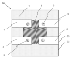
図1は、本発明の第1実施形態の半導体装置の断面図である。半導体装置10は、半導体チップ1とリード6と金属接合部5と封止樹脂7とを備える構成のフリップチップタイプのノンリード構造のパッケージであり、フリップチップタイプであるためボンディングワイヤやダイパッドを必要としない構造である。リード6は、一様の厚さの銅(Cu)または銅合金からなり、表面に支持面61、表面と反対側の裏面1bにリード底面62を有する。そして、支持面61には半導体チップ1が接続されている。半導体チップ1の主面1aに設けられた電極(図示せず)とリード6の支持面61に設けられた電極(図示せず)とが金(Au)を含有する金属接合部5を介して電気的に接続されているが、半導体チップ1は、その主面1aが下向きとなるように反転して接続されている。
1 is a cross-sectional view of a semiconductor device according to a first embodiment of the present invention. The
半導体チップ1とリード6と金属接合部5の周囲は封止樹脂7によって被覆されているが、リード底面62とリード側面63は封止樹脂7から露出している。半導体装置10は、断面視的に矩形であって、リード底面62は、封止樹脂7の樹脂底面72と面一であり、リード側面63は、封止樹脂7の樹脂側面73と面一である。そして、リード底面62およびリード側面63には基板実装のための外部端子11が被着されている。外部端子11は、リード底面62側やリード側面63側からニッケル(Ni)膜と金(Au)膜が順に被着している積層膜である。または、ニッケル(Ni)膜とパラジウム(Pd)膜と金(Au)膜が順に被着している積層膜である。
The
図2は、本発明の第1実施形態の半導体装置の底面図である。図2では、理解の便宜上、封止樹脂7を透視して図示している。半導体装置10は、4つのリード6を有するノンリード構造のパッケージであって、各リード6のおのおの一端は互いに離間して配置され、リード6の他端の端面は封止樹脂7の外囲と同一面をなしている。矩形の封止樹脂7の中央に半導体チップ1(破線で図示)が配置され、半導体チップ1の四隅がリード6のそれぞれと重畳している。半導体チップ1の四隅には電極が配置されるが、電極上には金属接合部5(破線で図示)があり、この金属接合部5を介して半導体チップ1とリード6とが接続されている。そして、半導体チップ1の四隅に配置された金属接合部5の平面領域はリード6の平面領域に含まれる形状である。
2 is a bottom view of the semiconductor device according to the first embodiment of the present invention. For ease of understanding, FIG. 2 shows the
図3は、半導体チップとリードの接合部の拡大断面図である。金属接合部5は、金(Au)を含有する合金であって、例えば金錫(AuSn)合金によって構成され、半導体チップ1側の金リッチ接合層5aを介して半導体チップ1側の電極3aと接続している。また、リード6側においても金リッチ接合層5bを介してリード6側の電極3bと接続している。電極3a、3bはバリア膜であるニッケル(Ni)膜4a、4bからなる。金リッチ接合層5a、5bのAu/Snの成分比率は金属接合部5のAu/Snの成分比率よりも高い、すなわち金(Au)含有率が高いものである。また、その金リッチ接合層5a、5b内での成分は一様ではなく、ニッケル膜4aに距離的に近いほどその比率は高いものである。半導体チップ1側の金属接合部5および金リッチ接合層5aの平面積に比べ、リード6側の金属接合部5および金リッチ接合層5bの平面積は大きくなっている。本図では、リード6の支持面61上の限定された一部の領域にニッケル膜4bを設けているが、支持面の全ての領域にバリア膜であるニッケル膜4bを被着させてもよい。
金属接合部5とニッケル膜4aとの間に位置する金リッチ接合層5a、5bは金属接合部5の構成成分が拡散して形成されたもので、形成される接合領域は強固なものである。また、半導体チップ1とリード6との厚さ方向の間隔は3~5μmであって極めて小さいものである。上述のように、半導体チップ1とリード6は強固に接続されているため、容易に剥離することはない。したがって、半導体チップ1は、その周囲が封止樹脂7によって完全に覆われているが、リード6の引き抜き強度が低下してリード6が封止樹脂7から脱落するといった懸念は無く、封止樹脂7からの脱落防止のための薄肉部を形成するというアンカー加工などは不要となる。このため、リード6にはアンカー加工に必要な厚みや幅が無くてもよく、リード6の板厚を薄く、小面積にすることができる。これにより、半導体装置の薄型化(低背化)、かつ小型化を実現することができる。また、アンカー加工という付加的な工程も必要とせず、製造における工数を減じることができる。
3 is an enlarged cross-sectional view of the joint between the semiconductor chip and the lead. The
The gold-
図4~図7を用いて、本発明の第1実施形態に係る半導体装置の製造方法について説明する。
まず、図4に示す半導体チップ1を用意する。図は、リード6と接続する前の半導体チップ1の上面図とパッド部の断面拡大図である。図4(a)に示すように、本例では、矩形の半導体チップ1の主面1aの四隅のおのおのにパッド2を覆うように4つの接合下地膜4が設けられている。図4(b)はパッド部の断面構造を示しており、半導体チップ1の主面1aにパッド2としてアルミ(Al)膜が形成されている。パッド2であるアルミ膜は半導体チップ1の最上層配線と同一層である。パッド2の上には接合下地膜4としてニッケル(Ni)膜4aと金(Au)膜44aが順に積層されている。ニッケル膜4aはバリア膜としての役目をし、金膜44aは濡れ性改善の役目を有する。空気中では酸化や腐食を発生し易いアルミ膜だが、その表面にニッケル膜4aと金膜44aを形成することによって酸化や腐食の発生し難い表面状態としている。なお、ニッケル膜4aと金膜44aは湿式のメッキ法(ニッケルメッキ、金フラッシュメッキ)によって形成されるのが好適である。パラジウム(Pd)膜を含む3層積層膜の場合は、ニッケルめっきとパラジウムめっきと金フラッシュめっきを順に施すことでパッド2上の接合下地膜4の形成が終了する。
A method for manufacturing a semiconductor device according to the first embodiment of the present invention will be described with reference to FIGS.
First, the
次に、半導体チップ1のパッド2上に、金(Au)を含み2種以上の金属からなる合金である接続材9を溶融状態でディスペンス(滴下塗布)する。図5は、パッド2上に接続材9をディスペンスする前後の状態を示す図である。図5(a)には、半導体チップ1と加熱ポッド12を図示している。加熱ポッド12は、加熱手段と脱気手段とディスペンス手段を有し、加熱ポッド12内に溶融した状態の接続材9が蓄えられている。接続材9は、金錫合金であって、例えば、Au/Sn=80/20、もしくはAu/Sn=78/22という成分比である。加熱手段によって加熱ポッド12は300~320℃に制御され、溶融状態の接続材9内の微小な気泡は脱気手段によって除去されている。また、有機物なども十分に脱媒されてる。加熱ポッド12の下端にはディスペンス手段が設けられ、その周囲は窒素パージされて、周囲の温度は室温である。半導体チップ1も加熱されることなく室温状態に保たれている。
Next, the connecting
図5(b)に示すように、溶融した接続材9が半導体チップ1のパッド2上の接合下地膜4の上にディスペンスされると溶融状態の接続材9は一定の表面張力を有するため、接合下地膜4上で一定の曲率を有する形状となっている。また、このときディスペンスされる接続材9のサイズは半導体チップ1のパッド2の大きさよりも小さいサイズである。
As shown in FIG. 5(b), when the molten connecting
なお、半導体チップ1上に接続材9をディスペンスする際、半導体チップ1は半導体ウェハからイシングして個片化したものが望ましい。ダイシング前の半導体チップ1に接続材9をディスペンスするほうが効率的であるが、ディスペンス後にダイシングをするとそのときに発生するカットゴミや水分に曝されることになる。これを回避するするためにダイシングの後に接続材9をディスペンスするという方法が好ましい。
When dispensing the
図5(c)では、半導体チップ1のパッド2上の接合下地膜4の上に接続材9がディスペンスされた後に、パッド2で固化された状態を示している。310~320℃でディスペンスされた溶融状態の接続材9はパッド2上の接合下地膜4と溶融したのち、室温に冷却されて以下の構造となる。すなわち、パッド2の上にはニッケル膜4aが積層され、ニッケル膜4aの上には金リッチ接合層5aが形成されている。金リッチ接合層5aは金属接合部5が金膜44aに拡散したものであり、その金リッチ接合層5aのAu/Snの成分比率は金属接合部5のAu/Snの成分比率よりも高い、すなわち金(Au)含有率が高いものである。また、その金リッチ接合層5a内での成分は一様ではなく、ニッケル膜4aに距離的に近いほどその比率は高いものである。
Figure 5 (c) shows the state where the
以上のような、個々のパッド2上の接合下地膜4の上に接続材9である溶融金錫をディスペンスすることを半導体チップ1上のすべてのパッド2に対し行うことで、金属接合部5と半導体チップ1との接続は完了する。このような方法によって得られる半導体チップ1と金属接合部5との接続は、従来の接続方法に比べ工数の少ない工程で行うことができる。例えば、バンプを形成するという従来の方法であれば、バンプ形成のためのレジストによるパターン形成工程やメッキ工程やレジスト除去工程、そしてリフロー工程というように数多くの工程を経ることになるが、本製造方法においては、予め溶融した接続材9をパッド2上の接合下地膜4の上にディスペンスするだけという極めて少ない工程で接続が完了する。また、特許文献1に示す従来の半導体装置における接続温度に比べ高温であるため、本製造方法によって得られる半導体チップ1と金属接合部5との接続は、ボイドの少ない強固な接続となる。
By dispensing the molten gold and
次に、図6に示すように、金属接合部5が設けられた半導体チップ1をリード6に接続する。図6(a)は、接続前の状態を図示するもので、リード6の上方に半導体チップ1が待機している。半導体チップ1の裏面1b側がコレット13を用いてピックアップされていて、金属接合部5が形成された半導体チップ1の主面1aが下向きに反転してリード6の支持面61に対向している。対向するリード6の支持面61の所定の箇所には、接合下地膜4としてニッケル(Ni)膜4bと金(Au)膜44bが順に積層されている。あるいは、ニッケル(Ni)膜とパラジウム(Pd)膜と金(Au)膜が順に積層されている。接合下地膜4の成膜方法は湿式のメッキ法によるものである。そして、半導体チップ1側に形成される接合下地膜4の平面積に比べ、リード6側の接合下地膜4の平面積は大きく形成されている。
Next, as shown in FIG. 6, the
対向するリード6の接合下地膜4の表面には有機溶剤14が点状に塗布されている。有機溶剤14が塗布される箇所は半導体チップ1が接続される位置にあたり、半導体チップ1をリード6に接続するときのセルフアライメントおよび仮固定の役目をする。このとき、半導体チップ1とリード6は、共に室温雰囲気に置かれている。
Organic solvent 14 is applied in dots to the surface of the
次に、半導体チップ1とともにコレット13を下降させ、半導体チップ1の金属接合部5を有機溶剤14が点状に塗布された箇所に当接するように重ね合わせする。このとき半導体チップ1とリード6の重ね合わせが多少ずれていたとしても有機溶剤14のセルフアライン効果を利用して半導体チップ1が微動して適正な位置へ補正配置されることになる。仮止め用の有機溶剤14としては、室温にて液体で加熱したときに蒸発するものがよく、イソプロピルアルコール(IPA)などのアルコール類やメチルエチルケトン(MEK)などのケトン類が好適である。以上では、有機溶剤14を用いた例にて説明したが、必ずしも有機溶剤14にて仮止めする工程は必須ではないが、本工程を用いることで、精度の高い重ね合わせが実現でき、より小型の半導体装置10とすることができる。
Next, the
その後、半導体チップ1を搭載したリード6を窒素雰囲気の加熱ステージに移動させ、リード6の裏面側から加熱する。本工程における加熱温度は半導体チップ1と金属接合部5の接続の時の温度よりも低いほうが良く、295~305℃が好適である。
Then, the
図6(b)に示すように、加熱によって有機溶剤14が蒸発するとともに金属接合部5が溶融して接合下地膜4と接続する。金属接合部5は接合下地膜4を構成する金膜44bに溶け込んで金リッチ接合層5bを形成し、半導体チップ1とリード6とを強固に接続する(図3参照)。なお、接続前の金属接合部5の表面は極めて薄い酸化膜で覆われているが、本方法によれば、従来のバンプ法と比較して高温での接続となるため、酸化膜除去と活性化を目的とするフラックス等を必要とせずとも非常に良好な濡れ広がりを得ることができる。
As shown in FIG. 6(b), the organic solvent 14 evaporates upon heating, and the metal joint 5 melts and connects to the
次に、半導体チップ1とリード6と金属接合部5とを封止樹脂7を被覆したのちに、必要に応じてリード6を成形する。リード底面62およびリード側面63の表面に外部端子11を形成する。外部端子11がニッケル(Ni)膜と金(Au)膜の積層膜の場合は、ニッケルめっきと金フラッシュめっきを順に施すことで外部端子11を形成できる。パラジウム(Pd)膜を含む3層積層膜の場合は、ニッケルめっきとパラジウムめっきと金フラッシュめっきを順に施すことで外部端子11を形成できる。以上の工程を経て、図1に示すような半導体装置10が完成する。
Next, the
特許文献1に示す従来の半導体装置では、金バンプをリードに接合する場合の温度は250℃程度であって、金バンプとリードとの間に形成される接合層は薄く島状である。このような従来の半導体装置をプリント基板へ実装する際にリフローを行うが、そのときの熱処理温度は255~265℃であって金バンプとリードとの接続温度よりも高い。そのためプリント基板実装によって金バンプからリード脱落する可能性があり、これを防止するためにリードの裏面側の周縁部にハーフエッチング領域(アンカー部)を設けている。これに対し、以上の工程を経て得られた半導体装置10の金属接合部5の熱処理温度(295℃以上)はプリント基板実装温度255~265℃よりも高く、プリント基板実装によって、金属接合部5が溶融して半導体チップ1とリード6との接続が弱くなってリード6が封止樹脂7から脱落する懸念はない。つまり、従来の半導体装置では必要とされたハーフエッチング領域を設けることなくリード脱落を防止できることになる。リードの周縁部にハーフエッチング領域を不要とすることで、リードが小さくなり半導体装置の小型化に貢献できる。また、ハーフエッチング領域は強度確保の点から所定の厚さを必要とするが、これを不要とすることからリードの厚さを減じることが可能となる。リードの厚さの薄型化は半導体装置の薄型化に貢献するものである。以上のように、ハーフエッチング領域を必要としない本発明の半導体装置ではさらなる小型化および薄型化が可能となる。
In the conventional semiconductor device shown in
なお、これまでは、金属接合部5や接続材9として金錫合金を用いた例について説明しているが、金錫合金に代えて金ゲルマニウム合金を用いた場合でも同様の効果が得られる。
Up to this point, we have described an example in which a gold-tin alloy is used as the
(第2実施形態)
図7は、本発明の第2実施形態の半導体装置の断面図である。図1に示した第1の実施形態の半導体装置においてはリード6の厚さは一様であったが、本実施形態の半導体装置20においてはリード側面63におけるリード厚さt1と半導体チップがリード6と接合する支持面61におけるリード厚さt2を異なる厚さとし、支持面61におけるリード厚さt2をリード側面63におけるリード厚さt1に比べ薄くしている。すなわち、リード6はリード側面63側、つまり、リード6の周縁側を厚肉領域66とし、半導体チップ1と接合する部分を薄肉領域67とする構造である。厚肉領域66および薄肉領域67の裏面は樹脂底面72とともに同一面を成し、厚肉領域66および薄肉領域67の上表面との間には段差部65が配置され、段差部65は順テーパの傾斜面である。そして、半導体チップ1は段差部65よりも内側、つまりリード6の薄肉領域67上に配置されている。また、このときの半導体チップ1の主面1aの樹脂底面72からの高さh1の値は、リード厚さt1の値よりも小さく、リード厚さt2の値よりも大きいものである。なお、本例における薄肉領域67は、第1の実施形態の半導体装置のような一様の厚さであるリードを上方から部分的にプレス加工やハーフエッチング加工して支持面61を形成することが可能である。ここでプレス加工等を施さない部分など、相対的にリードの厚さが厚い部分が厚肉領域66に相当する。
Second Embodiment
7 is a cross-sectional view of a semiconductor device according to a second embodiment of the present invention. In the semiconductor device according to the first embodiment shown in FIG. 1, the thickness of the
以上のように、リード6を厚肉領域66と薄肉領域67を有する形状とし、薄肉領域67の上に金属接合部5を介して半導体チップ1を搭載することで、プリント基板に対する半導体装置10の実装性を損なうことなく、半導体装置10の薄型化(低背化)を実現することができる。通常、プリント基板へ実装する際の接続領域は半導体装置10の外部端子11に相当するが、半導体装置10を薄型化すると、それに応じてリードの厚さが薄くなり、リード側面63に被着した外部端子11の面積が小さくなる。それに対応してプリント基板への半導体装置10の接続強度は小さくなる。これに対し、本実施形態の半導体装置20においてはリード6に厚肉領域66を設け、そこにリード側面63を形成しているため、リード側面63に被着している外部端子11の面積は小さくならず、プリント基板への接続強度が小さくなることはない。さらに、リード6の薄肉領域67に半導体チップ1を搭載する構造としているため、半導体装置10の薄型化を実現できる。また、半導体チップ1とリード6は強固な接続となっているため、リード6が封止樹脂7から脱落することを防止することができる。
As described above, by forming the
また、本半導体装置10の製造においては、半導体チップ1をリード6に接合する際に、図6で説明した有機溶剤14による仮止めを利用することになるが、この有機溶剤14の塗布範囲外に半導体チップ1の金属接合部5が置かれたとしてもリード6に設けられた段差部65によって誘導されて半導体チップ1が薄肉領域67に位置補正され、さらに、有機溶剤14によるセルフアラインによって位置を微調されることになる。このように、半導体チップ1をリード6上の適正な位置へ誘導する効果もあるため半導体装置のさらなる小型化へ貢献することができる。
In addition, in the manufacture of this
図7においては、半導体チップ1の主面1aの反対側である裏面1bの樹脂底面72からの高さh2が、リード厚さt1の値よりも大きい、すなわち、リード6の厚肉領域66の上面の樹脂底面72からの高さよりも大きい場合を図示しているが、半導体チップ1の厚さをさらに薄くすること、例えば半導体チップ1の裏面1bの樹脂底面72からの高さh2をリード6の厚肉領域66の上面の樹脂底面72からの高さよりも小さくすることで半導体装置10がさらに薄型化できることは明らかである。
Figure 7 shows a case where the height h2 from the
本発明による半導体装置は、携帯玩具、ヘルスケア商品、ウェアラブル端末、携帯端末、カード端末、家電製品等から、使用環境の厳しい車載用途、屋外用途への応用も可能である。 The semiconductor device according to the present invention can be used in a wide range of applications, from portable toys, healthcare products, wearable terminals, mobile terminals, card terminals, and home appliances to in-vehicle and outdoor applications in harsh operating environments.
1 半導体チップ
1a 主面
1b 裏面
2 パッド
3a、3b 電極
4 接合下地膜
4a、4b ニッケル膜(バリア膜)
44a、44b 金膜
5 金属接合部
5a、5b 金リッチ接合層
6 リード
61 支持面
62 リード底面
63 リード側面
65 段差部
66 厚肉領域
67 薄肉領域
7 封止樹脂
72 樹脂底面
73 樹脂側面
9 接続材
10、20 半導体装置
11 外部端子
12 加熱ポッド
13 コレット
14 有機溶剤
t1、t2 リード厚さ
h1、h2 樹脂底面からの高さ
Claims (4)
支持面とリード底面とリード側面とを有し、前記支持面に第2電極を有するリードと、
前記第1電極と前記第2電極とを接続する金属接合部と、
前記半導体チップと前記リードと前記金属接合部を封止する封止樹脂と、
前記リード底面および前記リード側面に形成され、前記封止樹脂から露出する外部端子と、
を備える半導体装置であって、
前記金属接合部は、金を含有する合金であって、前記合金よりも金含有率の高い第1金リッチ接合層を前記第1電極側に有し、前記合金よりも金含有率の高い第2金リッチ接合層を前記第2電極側に有し、
前記リードは、前記外部端子が形成された前記リード側面に設けられた厚肉領域と、前記厚肉領域から内側に延在する薄肉領域とからなり、前記薄肉領域上に前記半導体チップが搭載されていることを特徴とする半導体装置。 a semiconductor chip having a plurality of first electrodes;
a lead having a support surface, a lead bottom surface, and a lead side surface, the lead having a second electrode on the support surface;
a metal joint portion connecting the first electrode and the second electrode;
a sealing resin that seals the semiconductor chip, the leads, and the metal joints;
external terminals formed on the bottom surface and the side surface of the lead and exposed from the sealing resin;
A semiconductor device comprising:
The metal bonding portion is an alloy containing gold, and has a first gold-rich bonding layer on the first electrode side having a higher gold content than the alloy, and a second gold-rich bonding layer on the second electrode side having a higher gold content than the alloy,
The semiconductor device is characterized in that the lead comprises a thick region provided on the lead side on which the external terminal is formed, and a thin region extending inward from the thick region, and the semiconductor chip is mounted on the thin region .
前記半導体チップの主面に第1接合下地膜を形成する工程と、forming a first bonding underlayer film on a main surface of the semiconductor chip;
前記リードに厚肉領域と薄肉領域とを形成する工程と、forming thickened and thinned regions in the leads;
前記リードの前記薄肉領域の支持面に第2接合下地膜を形成する工程と、forming a second bonding undercoat on a support surface of the thinned region of the lead;
前記第1接合下地膜上に、溶融状態である接続材を塗布し、前記接続材を固化させて金属接合部を形成する工程と、applying a molten connection material onto the first bonding base film and solidifying the connection material to form a metal bond;
前記半導体チップの前記主面を前記リードの前記支持面の第2電極に対向させて重ね合わせする工程と、a step of overlapping the main surface of the semiconductor chip with the second electrode of the support surface of the lead;
前記リードを加熱して、前記半導体チップと前記リードとを前記金属接合部を介して接続する工程と、a step of heating the lead to connect the semiconductor chip and the lead via the metal joint;
前記半導体チップと前記リードと前記金属接合部を樹脂封止する工程と、a step of sealing the semiconductor chip, the leads, and the metal joints with resin;
前記リードに外部端子を設けることを特徴とする半導体装置の製造方法。A method of manufacturing a semiconductor device, comprising the steps of: providing an external terminal on said lead;
前記支持面上の前記第2接合下地膜上に有機溶剤を塗布する工程を設けることを特徴とする請求項3に記載の半導体装置の製造方法。4. The method for manufacturing a semiconductor device according to claim 3, further comprising the step of applying an organic solvent onto the second bonding underlayer film on the supporting surface.
Priority Applications (2)
| Application Number | Priority Date | Filing Date | Title |
|---|---|---|---|
| JP2021009987A JP7580282B2 (en) | 2021-01-26 | 2021-01-26 | Semiconductor device and its manufacturing method |
| US17/562,965 US11764131B2 (en) | 2021-01-26 | 2021-12-27 | Semiconductor device and manufacturing method thereof |
Applications Claiming Priority (1)
| Application Number | Priority Date | Filing Date | Title |
|---|---|---|---|
| JP2021009987A JP7580282B2 (en) | 2021-01-26 | 2021-01-26 | Semiconductor device and its manufacturing method |
Publications (2)
| Publication Number | Publication Date |
|---|---|
| JP2022113952A JP2022113952A (en) | 2022-08-05 |
| JP7580282B2 true JP7580282B2 (en) | 2024-11-11 |
Family
ID=82496032
Family Applications (1)
| Application Number | Title | Priority Date | Filing Date |
|---|---|---|---|
| JP2021009987A Active JP7580282B2 (en) | 2021-01-26 | 2021-01-26 | Semiconductor device and its manufacturing method |
Country Status (2)
| Country | Link |
|---|---|
| US (1) | US11764131B2 (en) |
| JP (1) | JP7580282B2 (en) |
Citations (7)
| Publication number | Priority date | Publication date | Assignee | Title |
|---|---|---|---|---|
| JP2004319993A (en) | 2003-03-28 | 2004-11-11 | Tamura Seisakusho Co Ltd | Electronic component mounting method and mounting device |
| US20060192295A1 (en) | 2004-11-17 | 2006-08-31 | Chippac, Inc. | Semiconductor package flip chip interconnect having spacer |
| JP2009135406A (en) | 2007-11-02 | 2009-06-18 | Dainippon Printing Co Ltd | Resin-sealed semiconductor device and etching member used therefor, method for manufacturing resin-sealed semiconductor device, and laminated resin-sealed semiconductor device |
| JP2013004929A (en) | 2011-06-21 | 2013-01-07 | Mitsubishi Materials Corp | Forming method of solder bump and paste for forming base |
| JP2016174117A (en) | 2015-03-18 | 2016-09-29 | ヤマハ株式会社 | Thermoelectric conversion module and manufacturing method thereof |
| JP2017135335A (en) | 2016-01-29 | 2017-08-03 | Shマテリアル株式会社 | Lead frame and semiconductor device, and method of manufacturing them |
| JP2019140179A (en) | 2018-02-07 | 2019-08-22 | 株式会社デンソー | Flip-chip mounting board and electronic equipment using the same |
Family Cites Families (16)
| Publication number | Priority date | Publication date | Assignee | Title |
|---|---|---|---|---|
| US4942454A (en) * | 1987-08-05 | 1990-07-17 | Mitsubishi Denki Kabushiki Kaisha | Resin sealed semiconductor device |
| US6194777B1 (en) * | 1998-06-27 | 2001-02-27 | Texas Instruments Incorporated | Leadframes with selective palladium plating |
| CN1190840C (en) * | 1999-04-08 | 2005-02-23 | 新光电气工业株式会社 | Lead frame for semiconductor device |
| KR100393448B1 (en) * | 2001-03-27 | 2003-08-02 | 앰코 테크놀로지 코리아 주식회사 | Semiconductor package and method for manufacturing the same |
| JP3841768B2 (en) * | 2003-05-22 | 2006-11-01 | 新光電気工業株式会社 | Package parts and semiconductor packages |
| TWI239087B (en) * | 2004-07-23 | 2005-09-01 | Siliconware Precision Industries Co Ltd | Flip-chip semiconductor package with lead frame and method for fabricating the same |
| US7268415B2 (en) * | 2004-11-09 | 2007-09-11 | Texas Instruments Incorporated | Semiconductor device having post-mold nickel/palladium/gold plated leads |
| US7358119B2 (en) * | 2005-01-12 | 2008-04-15 | Asat Ltd. | Thin array plastic package without die attach pad and process for fabricating the same |
| US7443015B2 (en) * | 2005-05-05 | 2008-10-28 | Stats Chippac Ltd. | Integrated circuit package system with downset lead |
| US8129229B1 (en) * | 2007-11-10 | 2012-03-06 | Utac Thai Limited | Method of manufacturing semiconductor package containing flip-chip arrangement |
| JP2013138261A (en) | 2009-09-29 | 2013-07-11 | Renesas Electronics Corp | Semiconductor device |
| JP5271949B2 (en) | 2009-09-29 | 2013-08-21 | ルネサスエレクトロニクス株式会社 | Semiconductor device |
| US20120313234A1 (en) * | 2011-06-10 | 2012-12-13 | Geng-Shin Shen | Qfn package and manufacturing process thereof |
| JP6784053B2 (en) | 2016-04-20 | 2020-11-11 | 富士通株式会社 | Manufacturing method of electronic device |
| DE102017108422A1 (en) * | 2017-04-20 | 2018-10-25 | Osram Opto Semiconductors Gmbh | Method for attaching a semiconductor chip to a leadframe and electronic component |
| JP7016677B2 (en) * | 2017-11-21 | 2022-02-07 | 新光電気工業株式会社 | Manufacturing method of lead frame, semiconductor device, lead frame |
-
2021
- 2021-01-26 JP JP2021009987A patent/JP7580282B2/en active Active
- 2021-12-27 US US17/562,965 patent/US11764131B2/en active Active
Patent Citations (7)
| Publication number | Priority date | Publication date | Assignee | Title |
|---|---|---|---|---|
| JP2004319993A (en) | 2003-03-28 | 2004-11-11 | Tamura Seisakusho Co Ltd | Electronic component mounting method and mounting device |
| US20060192295A1 (en) | 2004-11-17 | 2006-08-31 | Chippac, Inc. | Semiconductor package flip chip interconnect having spacer |
| JP2009135406A (en) | 2007-11-02 | 2009-06-18 | Dainippon Printing Co Ltd | Resin-sealed semiconductor device and etching member used therefor, method for manufacturing resin-sealed semiconductor device, and laminated resin-sealed semiconductor device |
| JP2013004929A (en) | 2011-06-21 | 2013-01-07 | Mitsubishi Materials Corp | Forming method of solder bump and paste for forming base |
| JP2016174117A (en) | 2015-03-18 | 2016-09-29 | ヤマハ株式会社 | Thermoelectric conversion module and manufacturing method thereof |
| JP2017135335A (en) | 2016-01-29 | 2017-08-03 | Shマテリアル株式会社 | Lead frame and semiconductor device, and method of manufacturing them |
| JP2019140179A (en) | 2018-02-07 | 2019-08-22 | 株式会社デンソー | Flip-chip mounting board and electronic equipment using the same |
Also Published As
| Publication number | Publication date |
|---|---|
| US11764131B2 (en) | 2023-09-19 |
| US20220238418A1 (en) | 2022-07-28 |
| JP2022113952A (en) | 2022-08-05 |
Similar Documents
| Publication | Publication Date | Title |
|---|---|---|
| US6943434B2 (en) | Method for maintaining solder thickness in flipchip attach packaging processes | |
| US11289409B2 (en) | Method for fabricating carrier-free semiconductor package | |
| US6162664A (en) | Method for fabricating a surface mounting type semiconductor chip package | |
| US7776653B2 (en) | Controlling flip-chip techniques for concurrent ball bonds in semiconductor devices | |
| US6781247B2 (en) | Semiconductor device | |
| TWI284973B (en) | Flip-chip joint structure, and fabricating process thereof | |
| US7656048B2 (en) | Encapsulated chip scale package having flip-chip on lead frame structure | |
| JPH08102466A (en) | Semiconductor device manufacturing method and semiconductor wafer | |
| JPH11204720A (en) | Semiconductor device and manufacturing method thereof | |
| US20050151268A1 (en) | Wafer-level assembly method for chip-size devices having flipped chips | |
| JP2002164498A (en) | Semiconductor device and manufacturing method thereof | |
| KR100592121B1 (en) | No-clean flux for flip chip assembly | |
| US9543239B2 (en) | Semiconductor device and production method therefor | |
| US6489180B1 (en) | Flip-chip packaging process utilizing no-flow underfill technique | |
| JP5035134B2 (en) | Electronic component mounting apparatus and manufacturing method thereof | |
| US20040089946A1 (en) | Chip size semiconductor package structure | |
| JP2005294443A (en) | Semiconductor device and manufacturing method thereof | |
| US20020095784A1 (en) | Bumping process for chip scale packaging | |
| US20080105960A1 (en) | Integrated Circuit Package and Method for Manufacturing an Integrated Circuit Package | |
| JP7580282B2 (en) | Semiconductor device and its manufacturing method | |
| US20080251937A1 (en) | Stackable semiconductor device and manufacturing method thereof | |
| JP2012190939A (en) | Semiconductor device and manufacturing method of the same | |
| JPH10214919A (en) | Manufacturing method of multi-chip module | |
| JP3443406B2 (en) | Resin-sealed semiconductor device | |
| JP2001094004A (en) | Semiconductor device, external connection terminal structure, and method of manufacturing semiconductor device |
Legal Events
| Date | Code | Title | Description |
|---|---|---|---|
| A621 | Written request for application examination |
Free format text: JAPANESE INTERMEDIATE CODE: A621 Effective date: 20231205 |
|
| A977 | Report on retrieval |
Free format text: JAPANESE INTERMEDIATE CODE: A971007 Effective date: 20240704 |
|
| A131 | Notification of reasons for refusal |
Free format text: JAPANESE INTERMEDIATE CODE: A131 Effective date: 20240801 |
|
| A521 | Request for written amendment filed |
Free format text: JAPANESE INTERMEDIATE CODE: A523 Effective date: 20240910 |
|
| TRDD | Decision of grant or rejection written | ||
| A01 | Written decision to grant a patent or to grant a registration (utility model) |
Free format text: JAPANESE INTERMEDIATE CODE: A01 Effective date: 20241022 |
|
| A61 | First payment of annual fees (during grant procedure) |
Free format text: JAPANESE INTERMEDIATE CODE: A61 Effective date: 20241029 |
|
| R150 | Certificate of patent or registration of utility model |
Ref document number: 7580282 Country of ref document: JP Free format text: JAPANESE INTERMEDIATE CODE: R150 |