JP7553130B2 - Laser device and method for manufacturing electronic device - Google Patents
Laser device and method for manufacturing electronic device Download PDFInfo
- Publication number
- JP7553130B2 JP7553130B2 JP2022556291A JP2022556291A JP7553130B2 JP 7553130 B2 JP7553130 B2 JP 7553130B2 JP 2022556291 A JP2022556291 A JP 2022556291A JP 2022556291 A JP2022556291 A JP 2022556291A JP 7553130 B2 JP7553130 B2 JP 7553130B2
- Authority
- JP
- Japan
- Prior art keywords
- wavelength
- command
- pulsed laser
- laser device
- laser light
- Prior art date
- Legal status (The legal status is an assumption and is not a legal conclusion. Google has not performed a legal analysis and makes no representation as to the accuracy of the status listed.)
- Active
Links
Images


Classifications
-
- G—PHYSICS
- G03—PHOTOGRAPHY; CINEMATOGRAPHY; ANALOGOUS TECHNIQUES USING WAVES OTHER THAN OPTICAL WAVES; ELECTROGRAPHY; HOLOGRAPHY
- G03F—PHOTOMECHANICAL PRODUCTION OF TEXTURED OR PATTERNED SURFACES, e.g. FOR PRINTING, FOR PROCESSING OF SEMICONDUCTOR DEVICES; MATERIALS THEREFOR; ORIGINALS THEREFOR; APPARATUS SPECIALLY ADAPTED THEREFOR
- G03F7/00—Photomechanical, e.g. photolithographic, production of textured or patterned surfaces, e.g. printing surfaces; Materials therefor, e.g. comprising photoresists; Apparatus specially adapted therefor
- G03F7/20—Exposure; Apparatus therefor
- G03F7/2002—Exposure; Apparatus therefor with visible light or UV light, through an original having an opaque pattern on a transparent support, e.g. film printing, projection printing; by reflection of visible or UV light from an original such as a printed image
- G03F7/2004—Exposure; Apparatus therefor with visible light or UV light, through an original having an opaque pattern on a transparent support, e.g. film printing, projection printing; by reflection of visible or UV light from an original such as a printed image characterised by the use of a particular light source, e.g. fluorescent lamps or deep UV light
- G03F7/2006—Exposure; Apparatus therefor with visible light or UV light, through an original having an opaque pattern on a transparent support, e.g. film printing, projection printing; by reflection of visible or UV light from an original such as a printed image characterised by the use of a particular light source, e.g. fluorescent lamps or deep UV light using coherent light; using polarised light
-
- G—PHYSICS
- G03—PHOTOGRAPHY; CINEMATOGRAPHY; ANALOGOUS TECHNIQUES USING WAVES OTHER THAN OPTICAL WAVES; ELECTROGRAPHY; HOLOGRAPHY
- G03F—PHOTOMECHANICAL PRODUCTION OF TEXTURED OR PATTERNED SURFACES, e.g. FOR PRINTING, FOR PROCESSING OF SEMICONDUCTOR DEVICES; MATERIALS THEREFOR; ORIGINALS THEREFOR; APPARATUS SPECIALLY ADAPTED THEREFOR
- G03F7/00—Photomechanical, e.g. photolithographic, production of textured or patterned surfaces, e.g. printing surfaces; Materials therefor, e.g. comprising photoresists; Apparatus specially adapted therefor
- G03F7/20—Exposure; Apparatus therefor
- G03F7/2002—Exposure; Apparatus therefor with visible light or UV light, through an original having an opaque pattern on a transparent support, e.g. film printing, projection printing; by reflection of visible or UV light from an original such as a printed image
- G03F7/201—Exposure; Apparatus therefor with visible light or UV light, through an original having an opaque pattern on a transparent support, e.g. film printing, projection printing; by reflection of visible or UV light from an original such as a printed image characterised by an oblique exposure; characterised by the use of plural sources; characterised by the rotation of the optical device; characterised by a relative movement of the optical device, the light source, the sensitive system or the mask
-
- G—PHYSICS
- G03—PHOTOGRAPHY; CINEMATOGRAPHY; ANALOGOUS TECHNIQUES USING WAVES OTHER THAN OPTICAL WAVES; ELECTROGRAPHY; HOLOGRAPHY
- G03F—PHOTOMECHANICAL PRODUCTION OF TEXTURED OR PATTERNED SURFACES, e.g. FOR PRINTING, FOR PROCESSING OF SEMICONDUCTOR DEVICES; MATERIALS THEREFOR; ORIGINALS THEREFOR; APPARATUS SPECIALLY ADAPTED THEREFOR
- G03F7/00—Photomechanical, e.g. photolithographic, production of textured or patterned surfaces, e.g. printing surfaces; Materials therefor, e.g. comprising photoresists; Apparatus specially adapted therefor
- G03F7/70—Microphotolithographic exposure; Apparatus therefor
- G03F7/70008—Production of exposure light, i.e. light sources
- G03F7/70025—Production of exposure light, i.e. light sources by lasers
-
- G—PHYSICS
- G03—PHOTOGRAPHY; CINEMATOGRAPHY; ANALOGOUS TECHNIQUES USING WAVES OTHER THAN OPTICAL WAVES; ELECTROGRAPHY; HOLOGRAPHY
- G03F—PHOTOMECHANICAL PRODUCTION OF TEXTURED OR PATTERNED SURFACES, e.g. FOR PRINTING, FOR PROCESSING OF SEMICONDUCTOR DEVICES; MATERIALS THEREFOR; ORIGINALS THEREFOR; APPARATUS SPECIALLY ADAPTED THEREFOR
- G03F7/00—Photomechanical, e.g. photolithographic, production of textured or patterned surfaces, e.g. printing surfaces; Materials therefor, e.g. comprising photoresists; Apparatus specially adapted therefor
- G03F7/70—Microphotolithographic exposure; Apparatus therefor
- G03F7/70483—Information management; Active and passive control; Testing; Wafer monitoring, e.g. pattern monitoring
- G03F7/7055—Exposure light control in all parts of the microlithographic apparatus, e.g. pulse length control or light interruption
- G03F7/70575—Wavelength control, e.g. control of bandwidth, multiple wavelength, selection of wavelength or matching of optical components to wavelength
-
- H—ELECTRICITY
- H01—ELECTRIC ELEMENTS
- H01S—DEVICES USING THE PROCESS OF LIGHT AMPLIFICATION BY STIMULATED EMISSION OF RADIATION [LASER] TO AMPLIFY OR GENERATE LIGHT; DEVICES USING STIMULATED EMISSION OF ELECTROMAGNETIC RADIATION IN WAVE RANGES OTHER THAN OPTICAL
- H01S3/00—Lasers, i.e. devices using stimulated emission of electromagnetic radiation in the infrared, visible or ultraviolet wave range
- H01S3/05—Construction or shape of optical resonators; Accommodation of active medium therein; Shape of active medium
- H01S3/08—Construction or shape of optical resonators or components thereof
- H01S3/08004—Construction or shape of optical resonators or components thereof incorporating a dispersive element, e.g. a prism for wavelength selection
- H01S3/08009—Construction or shape of optical resonators or components thereof incorporating a dispersive element, e.g. a prism for wavelength selection using a diffraction grating
-
- H—ELECTRICITY
- H01—ELECTRIC ELEMENTS
- H01S—DEVICES USING THE PROCESS OF LIGHT AMPLIFICATION BY STIMULATED EMISSION OF RADIATION [LASER] TO AMPLIFY OR GENERATE LIGHT; DEVICES USING STIMULATED EMISSION OF ELECTROMAGNETIC RADIATION IN WAVE RANGES OTHER THAN OPTICAL
- H01S3/00—Lasers, i.e. devices using stimulated emission of electromagnetic radiation in the infrared, visible or ultraviolet wave range
- H01S3/10—Controlling the intensity, frequency, phase, polarisation or direction of the emitted radiation, e.g. switching, gating, modulating or demodulating
- H01S3/13—Stabilisation of laser output parameters, e.g. frequency or amplitude
- H01S3/136—Stabilisation of laser output parameters, e.g. frequency or amplitude by controlling devices placed within the cavity
- H01S3/137—Stabilisation of laser output parameters, e.g. frequency or amplitude by controlling devices placed within the cavity for stabilising of frequency
-
- H—ELECTRICITY
- H01—ELECTRIC ELEMENTS
- H01S—DEVICES USING THE PROCESS OF LIGHT AMPLIFICATION BY STIMULATED EMISSION OF RADIATION [LASER] TO AMPLIFY OR GENERATE LIGHT; DEVICES USING STIMULATED EMISSION OF ELECTROMAGNETIC RADIATION IN WAVE RANGES OTHER THAN OPTICAL
- H01S3/00—Lasers, i.e. devices using stimulated emission of electromagnetic radiation in the infrared, visible or ultraviolet wave range
- H01S3/14—Lasers, i.e. devices using stimulated emission of electromagnetic radiation in the infrared, visible or ultraviolet wave range characterised by the material used as the active medium
- H01S3/22—Gases
- H01S3/223—Gases the active gas being polyatomic, i.e. containing two or more atoms
- H01S3/225—Gases the active gas being polyatomic, i.e. containing two or more atoms comprising an excimer or exciplex
- H01S3/2251—ArF, i.e. argon fluoride is comprised for lasing around 193 nm
-
- H—ELECTRICITY
- H01—ELECTRIC ELEMENTS
- H01S—DEVICES USING THE PROCESS OF LIGHT AMPLIFICATION BY STIMULATED EMISSION OF RADIATION [LASER] TO AMPLIFY OR GENERATE LIGHT; DEVICES USING STIMULATED EMISSION OF ELECTROMAGNETIC RADIATION IN WAVE RANGES OTHER THAN OPTICAL
- H01S3/00—Lasers, i.e. devices using stimulated emission of electromagnetic radiation in the infrared, visible or ultraviolet wave range
- H01S3/10—Controlling the intensity, frequency, phase, polarisation or direction of the emitted radiation, e.g. switching, gating, modulating or demodulating
- H01S3/13—Stabilisation of laser output parameters, e.g. frequency or amplitude
- H01S3/131—Stabilisation of laser output parameters, e.g. frequency or amplitude by controlling the active medium, e.g. by controlling the processes or apparatus for excitation
- H01S3/134—Stabilisation of laser output parameters, e.g. frequency or amplitude by controlling the active medium, e.g. by controlling the processes or apparatus for excitation in gas lasers
-
- H—ELECTRICITY
- H01—ELECTRIC ELEMENTS
- H01S—DEVICES USING THE PROCESS OF LIGHT AMPLIFICATION BY STIMULATED EMISSION OF RADIATION [LASER] TO AMPLIFY OR GENERATE LIGHT; DEVICES USING STIMULATED EMISSION OF ELECTROMAGNETIC RADIATION IN WAVE RANGES OTHER THAN OPTICAL
- H01S3/00—Lasers, i.e. devices using stimulated emission of electromagnetic radiation in the infrared, visible or ultraviolet wave range
- H01S3/10—Controlling the intensity, frequency, phase, polarisation or direction of the emitted radiation, e.g. switching, gating, modulating or demodulating
- H01S3/13—Stabilisation of laser output parameters, e.g. frequency or amplitude
- H01S3/139—Stabilisation of laser output parameters, e.g. frequency or amplitude by controlling the mutual position or the reflecting properties of the reflectors of the cavity, e.g. by controlling the cavity length
Landscapes
- Physics & Mathematics (AREA)
- Electromagnetism (AREA)
- Engineering & Computer Science (AREA)
- Plasma & Fusion (AREA)
- Optics & Photonics (AREA)
- General Physics & Mathematics (AREA)
- Lasers (AREA)
- Exposure And Positioning Against Photoresist Photosensitive Materials (AREA)
Description
本開示は、レーザ装置及び電子デバイスの製造方法に関する。 The present disclosure relates to methods for manufacturing laser devices and electronic devices.
近年、半導体露光装置においては、半導体集積回路の微細化及び高集積化につれて、解像力の向上が要請されている。このため、露光用光源から放出される光の短波長化が進められている。例えば、露光用のガスレーザ装置としては、波長約248nmのレーザ光を出力するKrFエキシマレーザ装置、並びに波長約193nmのレーザ光を出力するArFエキシマレーザ装置が用いられる。In recent years, there has been a demand for improved resolution in semiconductor exposure devices as semiconductor integrated circuits become finer and more highly integrated. This has led to efforts to shorten the wavelength of light emitted from exposure light sources. For example, gas laser devices used for exposure include KrF excimer laser devices that output laser light with a wavelength of approximately 248 nm and ArF excimer laser devices that output laser light with a wavelength of approximately 193 nm.
KrFエキシマレーザ装置及びArFエキシマレーザ装置の自然発振光のスペクトル線幅は、350~400pmと広い。そのため、KrF及びArFレーザ光のような紫外線を透過する材料で投影レンズを構成すると、色収差が発生してしまう場合がある。その結果、解像力が低下し得る。そこで、ガスレーザ装置から出力されるレーザ光のスペクトル線幅を、色収差が無視できる程度となるまで狭帯域化する必要がある。そのため、ガスレーザ装置のレーザ共振器内には、スペクトル線幅を狭帯域化するために、狭帯域化素子(エタロンやグレーティング等)を含む狭帯域化モジュール(Line Narrow Module:LNM)が備えられる場合がある。以下では、スペクトル線幅が狭帯域化されるガスレーザ装置を狭帯域化ガスレーザ装置という。The spectral linewidth of the spontaneous oscillation light of KrF excimer laser devices and ArF excimer laser devices is as wide as 350 to 400 pm. Therefore, if a projection lens is made of a material that transmits ultraviolet light, such as KrF and ArF laser light, chromatic aberration may occur. As a result, the resolution may decrease. Therefore, it is necessary to narrow the spectral linewidth of the laser light output from the gas laser device to a level where chromatic aberration can be ignored. Therefore, in order to narrow the spectral linewidth, a line narrow module (LNM) including a line narrowing element (such as an etalon or grating) may be provided in the laser resonator of the gas laser device. Hereinafter, a gas laser device in which the spectral linewidth is narrowed is referred to as a line narrowing gas laser device.
本開示の1つの観点に係るレーザ装置は、パルスレーザ光を出力する発振器と、パルスレーザ光の光路上に配置された光学素子と、光学素子を支持する回転ステージと、光学素子を介してパルスレーザ光が入射され、パルスレーザ光の入射角度に応じた波長の回折光を発振器に戻すように配置されたグレーティングと、回転ステージを駆動して光学素子を回転させることにより、パルスレーザ光のグレーティングへの入射角度を変更する第1駆動機構と、第1駆動機構よりも小さな駆動量で回転ステージを駆動して光学素子を回転させることにより、パルスレーザ光のグレーティングへの入射角度を変更する第2駆動機構と、パルスレーザ光の中心波長を計測する波長モニタと、パルスレーザ光の目標波長を周期的に変更し、目標波長と波長モニタの計測値とに基づいて、第2駆動機構に駆動指令を出力して入射角度を変更することにより、中心波長を目標波長に制御するプロセッサと、を備え、プロセッサは、目標波長を周期的に変更する波長指令周期の整数倍となる区間で第2駆動機構の駆動指令値の移動平均を算出し、算出された移動平均値が閾値を超えた場合に、第2駆動機構を初期位置に戻し、第2駆動機構を初期位置に戻すことによる入射角度の変化を第1駆動機構の駆動によって相殺させる。 A laser device according to one aspect of the present disclosure includes an oscillator that outputs pulsed laser light, an optical element arranged on the optical path of the pulsed laser light, a rotating stage that supports the optical element, a grating to which the pulsed laser light is incident via the optical element and which is arranged to return diffracted light of a wavelength corresponding to the angle of incidence of the pulsed laser light to the oscillator, a first driving mechanism that changes the angle of incidence of the pulsed laser light on the grating by driving the rotating stage to rotate the optical element, and a second driving mechanism that changes the angle of incidence of the pulsed laser light on the grating by driving the rotating stage with a smaller driving amount than the first driving mechanism to rotate the optical element. the first driving mechanism for periodically changing a target wavelength of the pulsed laser beam, a wavelength monitor for measuring a central wavelength of the pulsed laser beam, and a processor for periodically changing a target wavelength of the pulsed laser beam and outputting a drive command to the second driving mechanism to change the incident angle based on the target wavelength and a measurement value of the wavelength monitor, thereby controlling the central wavelength to the target wavelength, wherein the processor calculates a moving average of drive command values for the second driving mechanism in an interval which is an integer multiple of a wavelength command period for periodically changing the target wavelength, and when the calculated moving average value exceeds a threshold value, returns the second driving mechanism to an initial position and offsets the change in the incident angle caused by returning the second driving mechanism to its initial position by driving the first driving mechanism.
本開示の他の1つの観点に係る電子デバイスの製造方法は、パルスレーザ光を出力する発振器と、パルスレーザ光の光路上に配置された光学素子と、光学素子を支持する回転ステージと、光学素子を介してパルスレーザ光が入射され、パルスレーザ光の入射角度に応じた波長の回折光を発振器に戻すように配置されたグレーティングと、回転ステージを駆動して光学素子を回転させることにより、パルスレーザ光のグレーティングへの入射角度を変更する第1駆動機構と、第1駆動機構よりも小さな駆動量で回転ステージを駆動して光学素子を回転させることにより、パルスレーザ光のグレーティングへの入射角度を変更する第2駆動機構と、パルスレーザ光の中心波長を計測する波長モニタと、パルスレーザ光の目標波長を周期的に変更し、目標波長と波長モニタの計測値とに基づいて、第2駆動機構に駆動指令を出力して入射角度を変更することにより、中心波長を目標波長に制御するプロセッサと、を備え、プロセッサは、目標波長を周期的に変更する波長指令周期の整数倍となる区間で第2駆動機構の駆動指令値の移動平均を算出し、算出された移動平均値が閾値を超えた場合に、第2駆動機構を初期位置に戻し、第2駆動機構を初期位置に戻すことによる入射角度の変化を第1駆動機構の駆動によって相殺させる、レーザ装置によってレーザ光を生成し、レーザ光を露光装置に出力し、電子デバイスを製造するために、露光装置内で感光基板上にレーザ光を露光することを含む。A method for manufacturing an electronic device according to another aspect of the present disclosure includes an oscillator that outputs pulsed laser light, an optical element arranged on the optical path of the pulsed laser light, a rotating stage that supports the optical element, a grating arranged so that the pulsed laser light is incident through the optical element and diffracted light having a wavelength according to the angle of incidence of the pulsed laser light is returned to the oscillator, a first driving mechanism that changes the angle of incidence of the pulsed laser light on the grating by driving the rotating stage to rotate the optical element, a second driving mechanism that changes the angle of incidence of the pulsed laser light on the grating by driving the rotating stage with a smaller driving amount than the first driving mechanism to rotate the optical element, and a wavelength monitor that measures the central wavelength of the pulsed laser light. and a processor that periodically changes a target wavelength of the pulsed laser beam, and outputs a drive command to the second drive mechanism to change the angle of incidence based on the target wavelength and a measurement value of the wavelength monitor, thereby controlling the central wavelength to the target wavelength, wherein the processor calculates a moving average of a drive command value of the second drive mechanism in an interval which is an integer multiple of the wavelength command period for periodically changing the target wavelength, and when the calculated moving average value exceeds a threshold value, returns the second drive mechanism to an initial position, and offsets the change in the angle of incidence caused by returning the second drive mechanism to its initial position by driving the first drive mechanism; generating laser light by a laser device, outputting the laser light to an exposure device, and exposing the laser light onto a photosensitive substrate in the exposure device to manufacture an electronic device.
本開示の他の1つの観点に係るレーザ装置は、パルスレーザ光を出力する発振器と、パルスレーザ光の光路上に配置された第1光学素子と、第1光学素子を支持する第1回転ステージと、パルスレーザ光の光路上に配置された第2光学素子と、第2光学素子を支持する第2回転ステージと、第1光学素子及び第2光学素子を介してパルスレーザ光が入射され、パルスレーザ光の入射角度に応じた波長の回折光を発振器に戻すように配置されたグレーティングと、第1回転ステージを駆動して第1光学素子を回転させることにより、パルスレーザ光のグレーティングへの入射角度を変更する第1駆動機構と、第1駆動機構よりも小さな駆動量で第2回転ステージを駆動して第2光学素子を回転させることにより、パルスレーザ光のグレーティングへの入射角度を変更する第2駆動機構と、パルスレーザ光の中心波長を計測する波長モニタと、パルスレーザ光の目標波長を周期的に変更し、目標波長と波長モニタの計測値とに基づいて、第2駆動機構に駆動指令を出力して入射角度を変更することにより、中心波長を目標波長に制御するプロセッサと、を備え、プロセッサは、目標波長を周期的に変更する波長指令周期の整数倍となる区間で第2駆動機構の駆動指令値の移動平均を算出し、算出された移動平均値が閾値を超えた場合に、第2駆動機構を初期位置に戻し、第2駆動機構を初期位置に戻すことによる入射角度の変化を第1駆動機構の駆動によって相殺させる。A laser device according to another aspect of the present disclosure includes an oscillator that outputs pulsed laser light, a first optical element arranged on the optical path of the pulsed laser light, a first rotating stage that supports the first optical element, a second optical element arranged on the optical path of the pulsed laser light, a second rotating stage that supports the second optical element, a grating that receives the pulsed laser light via the first optical element and the second optical element and returns diffracted light of a wavelength according to the angle of incidence of the pulsed laser light to the oscillator, a first driving mechanism that changes the angle of incidence of the pulsed laser light on the grating by driving the first rotating stage to rotate the first optical element, and a second driving mechanism that drives the second rotating stage with a smaller driving amount than the first driving mechanism to change the angle of incidence of the pulsed laser light on the grating. a second driving mechanism that changes the angle of incidence of the pulsed laser beam on the grating by rotating a first driving mechanism, a wavelength monitor that measures a central wavelength of the pulsed laser beam, and a processor that controls the central wavelength to the target wavelength by periodically changing a target wavelength of the pulsed laser beam and outputting a driving command to the second driving mechanism based on the target wavelength and a measurement value of the wavelength monitor to change the angle of incidence, wherein the processor calculates a moving average of a driving command value for the second driving mechanism in an interval that is an integer multiple of a wavelength command period for periodically changing the target wavelength, and when the calculated moving average value exceeds a threshold value, returns the second driving mechanism to an initial position and offsets a change in the angle of incidence caused by returning the second driving mechanism to its initial position by driving the first driving mechanism.
本開示の他の1つの観点に係る電子デバイスの製造方法は、パルスレーザ光を出力する発振器と、パルスレーザ光の光路上に配置された第1光学素子と、第1光学素子を支持する第1回転ステージと、パルスレーザ光の光路上に配置された第2光学素子と、第2光学素子を支持する第2回転ステージと、第1光学素子及び第2光学素子を介してパルスレーザ光が入射され、パルスレーザ光の入射角度に応じた波長の回折光を発振器に戻すように配置されたグレーティングと、第1回転ステージを駆動して第1光学素子を回転させることにより、パルスレーザ光のグレーティングへの入射角度を変更する第1駆動機構と、第1駆動機構よりも小さな駆動量で第2回転ステージを駆動して第2光学素子を回転させることにより、パルスレーザ光のグレーティングへの入射角度を変更する第2駆動機構と、パルスレーザ光の中心波長を計測する波長モニタと、パルスレーザ光の目標波長を周期的に変更し、目標波長と波長モニタの計測値とに基づいて、第2駆動機構に駆動指令を出力して入射角度を変更することにより、中心波長を目標波長に制御するプロセッサと、を備え、プロセッサは、目標波長を周期的に変更する波長指令周期の整数倍となる区間で第2駆動機構の駆動指令値の移動平均を算出し、算出された移動平均値が閾値を超えた場合に、第2駆動機構を初期位置に戻し、第2駆動機構を初期位置に戻すことによる入射角度の変化を第1駆動機構の駆動によって相殺させる、レーザ装置によってレーザ光を生成し、レーザ光を露光装置に出力し、電子デバイスを製造するために、露光装置内で感光基板上にレーザ光を露光することを含む。A method for manufacturing an electronic device according to another aspect of the present disclosure includes an oscillator that outputs pulsed laser light, a first optical element arranged on the optical path of the pulsed laser light, a first rotating stage that supports the first optical element, a second optical element arranged on the optical path of the pulsed laser light, a second rotating stage that supports the second optical element, a grating into which the pulsed laser light is incident via the first optical element and the second optical element, and which is arranged to return diffracted light of a wavelength according to the angle of incidence of the pulsed laser light to the oscillator, a first driving mechanism that changes the angle of incidence of the pulsed laser light on the grating by driving the first rotating stage to rotate the first optical element, and a second driving mechanism that changes the angle of incidence of the pulsed laser light on the grating by driving the second rotating stage with a smaller driving amount than the first driving mechanism to rotate the second optical element. the first driving mechanism for changing the incident angle of the first driving mechanism based on the target wavelength and the measurement value of the wavelength monitor; and a processor for periodically changing a target wavelength of the pulsed laser beam and outputting a driving command to the second driving mechanism to change the incident angle based on the target wavelength and the measurement value of the wavelength monitor, thereby controlling the central wavelength to the target wavelength, wherein the processor calculates a moving average of a driving command value of the second driving mechanism in an interval which is an integer multiple of a wavelength command period for periodically changing the target wavelength, and when the calculated moving average value exceeds a threshold value, returns the second driving mechanism to an initial position and offsets a change in the incident angle caused by returning the second driving mechanism to its initial position by driving the first driving mechanism; generating laser light by a laser apparatus, outputting the laser light to an exposure apparatus, and exposing the laser light onto a photosensitive substrate in the exposure apparatus to manufacture an electronic device.
本開示のいくつかの実施形態を、単なる例として、添付の図面を参照して以下に説明する。
-目次-
1.用語の説明
1.1 Nスリットの説明
1.2 バーストパルスの説明
1.3 その他の用語について
2.比較例に係るエキシマレーザ装置の概要
2.1 構成
2.2 動作
2.3 課題
3.実施形態1
3.1 構成
3.2 動作
3.3 制御例を示すフローチャートの説明
3.4 作用・効果
4.実施形態2
4.1 構成
4.2 動作
4.3 作用・効果
5.実施形態3
5.1 構成
5.2 動作
5.3 ヒステリシス補正の制御例
5.4 調整発振と本露光とを含む一連の動作の制御例
5.5 作用・効果
6.実施形態4
6.1 構成
6.2 動作
6.3 作用・効果
7.実施形態5
7.1 構成
7.2 動作
7.3 作用・効果
8.電子デバイスの製造方法について
9.その他
以下、本開示の実施形態について、図面を参照しながら詳しく説明する。以下に説明される実施形態は、本開示のいくつかの例を示すものであって、本開示の内容を限定するものではない。また、各実施形態で説明される構成及び動作の全てが本開示の構成及び動作として必須であるとは限らない。なお、同一の構成要素には同一の参照符号を付して、重複する説明を省略する。
-table of contents-
1. Explanation of terms 1.1 Explanation of N slit 1.2 Explanation of burst pulse 1.3
3.1 Configuration 3.2 Operation 3.3 Description of a flow chart showing a control example 3.4 Functions and
4.1 Configuration 4.2 Operation 4.3 Effects and
5.1 Configuration 5.2 Operation 5.3 Example of control of hysteresis correction 5.4 Example of control of a series of operations including adjustment oscillation and main exposure 5.5 Functions and
6.1 Configuration 6.2 Operation 6.3 Effects and
7.1 Configuration 7.2 Operation 7.3 Actions and
1.用語の説明
1.1 Nスリットの説明
図1は、ウエハWF上でのステップアンドスキャン露光の露光パターンの例を示す。図1のウエハWF内に示す多数の矩形領域のそれぞれはスキャンフィールドSFである。スキャンフィールドSFは、1回のスキャン露光の露光領域であり、スキャン領域とも呼ばれる。ウエハ露光は、図1に示すように、ウエハWFを複数の所定サイズの露光領域(スキャンフィールド)に分割して、ウエハ露光の開始(Wafer START)と終了(Wafer END)との間の期間に、各露光領域をスキャン露光することにより行われる。
1. Explanation of Terms 1.1 Explanation of N-Slits FIG. 1 shows an example of an exposure pattern for step-and-scan exposure on a wafer WF. Each of the many rectangular areas shown in the wafer WF in FIG. 1 is a scan field SF. A scan field SF is an exposure area for one scan exposure, and is also called a scan area. As shown in FIG. 1, wafer exposure is performed by dividing the wafer WF into a plurality of exposure areas (scan fields) of a predetermined size, and performing scan exposure on each exposure area during the period between the start (Wafer START) and end (Wafer END) of wafer exposure.
すなわち、ウエハ露光では、ウエハWFの第1の所定の露光領域を1回目のスキャン露光(Scan#1)で露光し、次いで、第2の所定の露光領域を2回目のスキャン露光(Scan#2)で露光するというステップを繰り返す。1回のスキャン露光中は、複数のパルスレーザ光が連続的にレーザ装置から出力され得る。このスキャン露光を順次繰り返し、1枚目のウエハWFの全露光領域をスキャン露光し終えたら、再度、調整発振を行った後、2枚目のウエハWFのウエハ露光が行われる。That is, in wafer exposure, a first predetermined exposure area of the wafer WF is exposed by a first scan exposure (Scan #1), and then a second predetermined exposure area is exposed by a second scan exposure (Scan #2), and this step is repeated. During one scan exposure, multiple pulsed laser beams can be continuously output from the laser device. This scan exposure is repeated sequentially, and when the entire exposure area of the first wafer WF has been scanned and exposed, adjustment oscillation is performed again, and then wafer exposure of the second wafer WF is performed.
図1に示す破線矢印の順番で、Wafer START→Scan#1→Scan#2→・・・・・・・→Scan#126→Wafer ENDまでステップアンドスキャン露光される。ウエハWFはレジストが塗布された半導体基板(感光基板)の一例である。
Step-and-scan exposure is performed in the order of the dashed arrows shown in Figure 1, from Wafer START
図2は、ウエハWF上の1つのスキャンフィールドSFとスキャンビームSBとの関係を示す。スキャンビームSBは、スキャンフィールドSFに対するスキャン露光に用いられる概ね長方形の光強度分布が略均一なビーム照射領域である。照明光学系によって整形された概ね長方形の略均一なビームがレチクル上に照射され、ビームの短軸方向(ここではY軸方向)に、レチクルとウエハWFとが投影光学系の縮小倍率に応じて、Y軸方向に互いに異なる向きで移動しながら露光が行われる。これにより、ウエハWF上の各スキャンフィールドSFにレチクルパターンがスキャン露光される。 Figure 2 shows the relationship between one scan field SF on the wafer WF and the scan beam SB. The scan beam SB is a roughly rectangular beam irradiation area with a roughly uniform light intensity distribution used for scan exposure of the scan field SF. A roughly rectangular, roughly uniform beam shaped by the illumination optical system is irradiated onto the reticle, and exposure is performed while the reticle and wafer WF move in different directions in the Y-axis direction in the short axis direction of the beam (here, the Y-axis direction) depending on the reduction magnification of the projection optical system. This causes the reticle pattern to be scan-exposed onto each scan field SF on the wafer WF.
図2において、縦方向の上向きのY軸方向マイナス側に向かう方向がスキャン方向であり、Y軸方向プラス側に向かう方向がウエハ移動方向(ステージ移動方向)である。図2の紙面に平行でY軸方向と直交する方向(X軸方向)をスキャン幅方向という。ウエハWF上でのスキャンフィールドSFのサイズは、例えば、Y軸方向が33mm、X軸方向が26mmである。 In Figure 2, the vertical direction upward toward the negative Y-axis direction is the scan direction, and the direction toward the positive Y-axis direction is the wafer movement direction (stage movement direction). The direction parallel to the paper surface of Figure 2 and perpendicular to the Y-axis direction (X-axis direction) is called the scan width direction. The size of the scan field SF on the wafer WF is, for example, 33 mm in the Y-axis direction and 26 mm in the X-axis direction.
図3は、スキャンビームSBの照射エリアの例を示す。スキャンビームSBのX軸方向の長さをBx、Y軸方向の幅をByとすると、BxはスキャンフィールドSFのX軸方向のサイズに対応しており、ByはスキャンフィールドSFのY軸方向のサイズよりも十分に小さいものとなっている。 Figure 3 shows an example of the irradiation area of the scan beam SB. If the length of the scan beam SB in the X-axis direction is Bx and the width in the Y-axis direction is By, Bx corresponds to the size of the scan field SF in the X-axis direction, and By is sufficiently smaller than the size of the scan field SF in the Y-axis direction.
スキャンビームSBは、パルスレーザ光の1パルスが照射するエリアであり、Nスリットと呼ばれる。スキャン露光によりウエハWF上の1箇所あたりに照射されるパルス数をNスリットパルス数NSLとする。Nスリットパルス数NSLは次式で表される。 The scan beam SB is an area irradiated with one pulse of the pulsed laser light, and is called N slit. The number of pulses irradiated to one location on the wafer WF by the scan exposure is the N slit pulse number N SL . The N slit pulse number N SL is expressed by the following formula.
NSL=(By/Vy)・f
Vy:ウエハのY軸方向のスキャン速度
f:レーザの繰り返し周波数(Hz)
同一のスキャンフィールドSFを複数の波長で露光する場合は、Nスリットパルス数NSLを1周期としてNスリット内で波長を変化させる必要がある。
NSL = (By/Vy)・f
Vy: Scanning speed of the wafer in the Y-axis direction f: Laser repetition frequency (Hz)
When exposing the same scan field SF with a plurality of wavelengths, it is necessary to change the wavelength within the N slits, with the number of N slit pulses NSL being one period.
1.2 バーストパルスの説明
図4は、バーストパルスの例を示すグラフである。横軸はパルス数、縦軸は波長を表す。ウエハWFを露光するときに1つのスキャンフィールドSFのスキャン露光が終ると、パルス生成を休止してステージを駆動させて次のスキャンフィールドSFに移動してスキャン露光を行う。この場合、パルス波形は図4に示すように一定の間隔で照射される一連のパルスと、休止期間とが交互に繰り返されるようになる。このようなパルスの態様をバーストパルスという。
1.2 Description of Burst Pulse Figure 4 is a graph showing an example of a burst pulse. The horizontal axis represents the number of pulses, and the vertical axis represents the wavelength. When the scan exposure of one scan field SF is completed during exposure of the wafer WF, pulse generation is stopped and the stage is driven to move to the next scan field SF and perform scan exposure. In this case, the pulse waveform alternates between a series of pulses irradiated at regular intervals and pause periods, as shown in Figure 4. This type of pulse form is called a burst pulse.
図4には、同一のスキャンフィールドSFを2波長(波長λ1、λ2)で露光する例が示されている。ここでは、Nスリットパルス数NSLが10パルスの例を示し、10パルスを1周期として、この周期T内で前半5パルスの目標波長がλ1、後半5パルスの目標波長がλ2である場合を説明するが、周期TとしてのNスリットパルス数NSL、2波長の切り替えタイミング及びスキャンフィールドSFの露光に必要なパルス数については図4の例に限らない。例えば、Nスリットパルス数NSLは30パルスであってもよい。 4 shows an example of exposing the same scan field SF with two wavelengths (wavelengths λ1 and λ2). Here, an example is shown in which the N slit pulse number N SL is 10 pulses, and a case is described in which 10 pulses are one cycle, and the target wavelength of the first five pulses in this cycle T is λ1 and the target wavelength of the latter five pulses is λ2. However, the N slit pulse number N SL as the cycle T, the timing of switching between the two wavelengths, and the number of pulses required for exposure of the scan field SF are not limited to the example in FIG. 4. For example, the N slit pulse number N SL may be 30 pulses.
1.3 その他の用語について
「ピエゾ素子」は、圧電素子と同義である。ピエゾ素子を単に「ピエゾ」と表記する場合がある。
1.3 Other terms "Piezo element" is synonymous with piezoelectric element. Piezo element may be simply written as "piezo".
本明細書における「平行」という用語には、技術的意義において実質的に平行と同等の範囲と見做しうる略平行の概念が含まれてよい。また、本明細書における「垂直」又は「直交」という用語には、技術的意義において実質的に垂直又は実質的に直交と同等の範囲と見做しうる略垂直又は略直交の概念が含まれてよい。The term "parallel" in this specification may include the concept of approximately parallel, which may be considered to be in the same range as substantially parallel in the technical sense. Furthermore, the terms "vertical" and "orthogonal" in this specification may include the concept of approximately perpendicular or approximately orthogonal, which may be considered to be in the same range as substantially perpendicular or substantially orthogonal in the technical sense.
2.比較例に係るエキシマレーザ装置の概要
2.1 構成
図5は、比較例に係るエキシマレーザ装置11の構成を概略的に示す。本開示の比較例とは、出願人のみによって知られていると出願人が認識している形態であって、出願人が自認している公知例ではない。エキシマレーザ装置11は、レーザ媒質であるレーザガスを封入したレーザチャンバ12を備えている。レーザチャンバ12の両端部には、パルスレーザ光21を透過するフロントウィンドウ17及びリアウィンドウ19が、それぞれ図示しないホルダを介して配置されている。
2. Overview of the excimer laser device according to the comparative example 2.1 Configuration Figure 5 shows a schematic configuration of an
レーザチャンバ12の内部には、一対の放電電極14,15が、図5中の紙面と垂直方向に対向して配置されている。高圧電源23から放電電極14,15間に高電圧を印加し、パルス放電を発生させてレーザガスを励起することにより、例えば数kHzから十数kHzの周波数でパルスレーザ光21を発生させる。Inside the
発生したパルスレーザ光21は、例えばレーザチャンバ12の後方(図5中の左方)へ進行し、パルスレーザ光21を狭帯域化する狭帯域化ユニット30に入射する。狭帯域化ユニット30は、狭帯域化ボックス31によって囲まれており、内部に光学素子として、プリズム32,32、波長選択ミラー34及びグレーティング33等を備えている。The generated pulsed
狭帯域化ボックス31の壁には、パージガス供給口35が設けられている。パージガス供給口35から清浄で乾燥した希ガスや高純度窒素などの反応性の低いパージガス45が狭帯域化ボックス31内部に導入される。A purge
狭帯域化ユニット30に入射したパルスレーザ光21は、プリズム32,32によって拡大され、波長選択ミラー34によって反射され、狭帯域化光学素子であるグレーティング33に入射する。グレーティング33では、回折によって、入射角度φによって定まる中心波長λcのパルスレーザ光21のみが反射される。すなわち、グレーティング33は、入射したパルスレーザ光21のうち入射角度φに応じた中心波長λcの回折光がレーザチャンバ12に戻るようにリトロー配置されている。The
波長選択ミラー34は、水平面内(図5中の紙面と平行な平面内)で回動自在の可動ホルダ36に搭載されている。可動ホルダ36を回転させて波長選択ミラー34を回転させることにより、グレーティング33に入射するパルスレーザ光21の入射角度φが変わる。これにより、グレーティング33で回折されるパルスレーザ光21の中心波長λcが変化する。なお、図5において、符号20はパルスレーザ光21のレーザ光軸を表している。The
狭帯域化されたパルスレーザ光21は、狭帯域化ユニット30内のグレーティング33と、パルスレーザ光21を部分反射するフロントミラー16との間で数回往復するうちに、放電電極14,15間の放電によって増幅される。そして、フロントミラー16を部分透過し、パルスレーザ光21として前方(図5中の右方)へ出射し、露光装置25に入射する。出射したパルスレーザ光21の一部は、ビームスプリッタ22で図5中の下方へ取り出され、波長モニタ37によってその中心波長λcがモニタリングされる。The narrow-band
以下、可動ホルダ36の構造について説明する。図6は、可動ホルダ36の平面断面図である。図7は、狭帯域化ボックス31内部のグレーティング33側から波長選択ミラー34側を見た可動ホルダ36の正面図である。図6及び図7に示すように、可動ホルダ36は、波長選択ミラー34を固定した四角形のミラーホルダ38を備えている。ミラーホルダ38は、図示しない引きバネ及び板バネ49の付勢力によって、狭帯域化ボックス31に引きつけられている。The structure of the
また、ミラーホルダ38の四隅の第1隅部38Aから第4隅部38Dのうち、第1隅部38Aと第2隅部38Bとは、それぞれ手動マイクロメータ50及び支持部材39によって、狭帯域化ボックス31から押圧されている。支持部材39は、例えばスクリュー47を所定長さだけ狭帯域化ボックス31から突き出させ、ナット46で固定している。また、手動マイクロメータ50は、手動で狭帯域化ボックス31からの突き出し量を変更自在である。Of the four corners of the
ミラーホルダ38の第3隅部38Cには、後述するようにピエゾ素子ユニット41が取り付けられている。ピエゾ素子ユニット41の先端部41Bは、図示しない引きバネ及び板バネ49の付勢力によってボールネジユニット43と接し、ステッピングモータユニット40を押圧している。ピエゾ素子ユニット41は、ピエゾ素子を含む微動駆動機構である。ステッピングモータユニット40は、ステッピングモータを含む粗動駆動機構である。
A
また、図5に示すように、ステッピングモータユニット40及びピエゾ素子ユニット41は、いずれもプロセッサ29に電気的に接続されている。プロセッサ29は、エキシマレーザ装置11全体を制御するレーザコントローラとして機能する。本開示のプロセッサ29とは、制御プログラムが記憶された記憶装置と、制御プログラムを実行するCPU(Central Processing Unit)とを含む処理装置である。プロセッサ29は本開示に含まれる各種処理を実行するために特別に構成又はプログラムされている。
As shown in FIG. 5, the stepping
ステッピングモータユニット40は、プロセッサ29から受信したパルス信号のパルス数に応じて、モータ軸48(図6参照)を所定量だけ回転させる。モータ軸48の先端部48Aには、カップリング42を介して、ネジ山が精密加工されたボールネジユニット43の後端部43Bが取着されている。ボールネジユニット43は、ガイド51によって、回転しながら前後方向にスムーズに直進運動を行う。The stepping
ボールネジユニット43の先端部43Aは、その長手方向に垂直な平面に精密加工され、この平面に、球面に精密加工されたピエゾ素子ユニット41の先端部41Bが当接している。従って、ボールネジユニット43が回転しながら前後動したとき、ピエゾ素子ユニット41は回転せずに前後動する。ピエゾ素子ユニット41の後端部41Aは、ミラーホルダ38に固定された紫外線カバー44に固定されている。The
ピエゾ素子ユニット41の配線52は、紫外線カバー44の内側を通って、図示しない導入孔を介して狭帯域化ボックス31の外部に達しており、プロセッサ29に接続されている。ピエゾ素子ユニット41は、配線52を介して印加された、電圧Vの大きさに応じた長さだけ、前後方向に伸縮する。The
ピエゾ素子ユニット41のフルストロークの約1/2の位置を、中立位置という。ピエゾ素子ユニット41を中立位置まで伸長させる電圧Vを、中立電圧V0という。プロセッサ29は、中立電圧V0をピエゾ素子ユニット41に常時印加している。これにより、ピエゾ素子ユニット41は、初期位置として中立位置に保たれている。The position of approximately half of the full stroke of the
プロセッサ29は、可動ホルダ36に信号を出力してステッピングモータユニット40又はピエゾ素子ユニット41を伸縮させることにより、紫外線カバー44を介してミラーホルダ38の第3隅部38Cを押し引きする。これにより、波長選択ミラー34が回動し、入射角度φが変更されて、パルスレーザ光21の中心波長λcが変化する。The
このときプロセッサ29は、波長モニタ37によってモニタリングした中心波長λcに基づき、中心波長λcと目標波長λ0との差である波長偏差Δλが所定の許容範囲よりも小さくなるように、波長制御を行っている。以下の説明では、波長偏差Δλを所定の許容範囲よりも小さくなるように波長制御することを、中心波長λcを目標波長λ0に合わせると言う。At this time, the
また、プロセッサ29は、高圧電源23に指令を出力することにより、パルスレーザ光21のパルス出力の制御も行っている。さらにプロセッサ29は、露光装置25と互いに通信を行っており、露光装置25から発振指令信号に基づいてレーザ発振を行う。また、プロセッサ29は、自己の判断に基づいて発振指令信号を出力し、レーザ発振を行う場合もある。The
2.2 動作
露光装置25でレジスト膜にパルスレーザ光21を照射する際に、焦点深度を大きくするために複数の波長で露光することが知られている。焦点深度を大きくすると、膜厚の大きいレジスト膜を露光する場合でも、レジスト膜の厚み方向での結像性能を維持することができる。
2.2 Operation It is known that exposure is performed with a plurality of wavelengths in order to increase the depth of focus when the resist film is irradiated with the
複数の波長で露光する手段として、エキシマレーザ装置11で生成されるパルスレーザ光21の波長を、例えば長波長と短波長との2つの波長で周期的に切り替えることが知られている(図4参照)。目標波長として波長λ1と波長λ2とを設定し、これら2波長を周期的に切り替える場合の動作の例は次の通りである。As a means for exposing at multiple wavelengths, it is known to periodically switch the wavelength of the
[手順1]プロセッサ29は、露光装置25から2波長の目標波長λ1、λ2と、波長を制御する周期Tを受信する。周期Tは1周期分のパルス数で表される。この周期Tを表すパルス数は、ウエハWF上のレジスト膜の同一箇所に照射されるパルス数、すなわちNスリットパルス数NSLであってよい。
[Step 1] The
[手順2]プロセッサ29は、受信した目標波長λ1となるように、ピエゾ素子ユニット41又はステッピングモータユニット40を駆動させて波長選択ミラー34を回転させて、グレーティング33に入射するパルスレーザ光21の入射角度φを変化させる。
[Step 2] The
[手順3]狭帯域化されたパルスレーザ光21は、ビームスプリッタ22によって一部が取り出され、波長モニタ37により波長が計測される。
[Step 3] A portion of the narrowband
[手順4]プロセッサ29は、計測された波長(中心波長λc)が目標波長λ1に対してずれている場合は、高速応答性に優れるピエゾ素子ユニット41を駆動させて、中心波長λcが目標波長λ1に近づくように波長選択ミラー34の姿勢を調整する。手順4のフィードバック制御はパルス毎に行われる。
[Step 4] If the measured wavelength (center wavelength λc) deviates from the target wavelength λ1, the
[手順5]プロセッサ29は、波長を切り替えるタイミングになると、パルスレーザ光21の波長が目標波長λ2となるように、ピエゾ素子ユニット41を駆動させて波長選択ミラー34を回転させ、グレーティング33に入射するパルスレーザ光21の入射角度φを変化させる。
[Step 5] When it is time to switch the wavelength, the
[手順6]手順5の動作により生成されたパルスレーザ光21は、ビームスプリッタ22によって一部が取り出され、波長モニタ37により波長が計測される。
[Step 6] A portion of the
[手順7]プロセッサ29は、計測された波長が目標波長λ2に対してずれている場合は、ピエゾ素子ユニット41を駆動させて、中心波長λcが目標波長λ2に近づくように波長選択ミラー34の姿勢を調整する。手順7のフィードバック制御もパルス毎に行われる。
[Step 7] If the measured wavelength deviates from the target wavelength λ2, the
[手順8]プロセッサ29は、波長を切り替えるタイミングになると、目標波長λ1となるように、ピエゾ素子ユニット41を駆動させて波長選択ミラー34を回転させて、グレーティング33に入射するパルスレーザ光21の入射角度φを変化させる。
[Step 8] When it is time to switch the wavelength, the
以下、上記の手順3~8が繰り返される。 Then, steps 3 to 8 above are repeated.
2.3 課題
狭帯域化ユニット30に用いられているピエゾ素子は温度の影響を受けるため、時間経過とともに入力に対する出力が変動(ドリフト)していく。そのためピエゾ指令はフィードバック制御によりパルス毎に補正されるが、ピエゾ素子が作動限界に到達するとそれ以上波長選択ミラー34の角度が調整できなくなることがあり得る。
2.3 Issues The piezoelectric element used in the
そこで、ピエゾ指令値が所定の閾値に到達したらステッピングモータを駆動して波長選択ミラー34の姿勢を調整し、ピエゾ素子を中立位置に戻すことが考えられる。Therefore, when the piezoelectric command value reaches a predetermined threshold value, it is possible to drive the stepping motor to adjust the posture of the
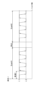
しかしながら、図8及び図9に示すように、目標波長をλ1からλ2に切り替えたときには既に、ピエゾ指令値が閾値及び作動限界を超えていて、動作不能となることがあり得た。However, as shown in Figures 8 and 9, when the target wavelength was switched from λ1 to λ2, the piezoelectric command value had already exceeded the threshold value and operating limit, and it was possible that the device would become inoperable.
図8は、2波長を切り替えるバーストパルスの例である。横軸はパルス数、縦軸は波長を表す。ここでは図4と同様に、10パルスの周期Tにおける前半5パルスの目標波長をλ1、後半5パルスの目標波長をλ2とする例を示す。図9は、図8に示す2波長の切り替え制御に対応するピエゾ指令の例を示す。横軸はパルス数であり、縦軸はピエゾ指令値を表す。図9の横軸は、図8の横軸と同じパルス数の範囲を同じスケールで示す。図8に示すように、目標波長がλ1とλ2との2波長で不連続に変化することに対応して、図9に示すようにピエゾ指令も不連続に変化する。 Figure 8 is an example of a burst pulse that switches between two wavelengths. The horizontal axis represents the number of pulses, and the vertical axis represents the wavelength. As in Figure 4, an example is shown here in which the target wavelength for the first five pulses in a period T of 10 pulses is λ1, and the target wavelength for the last five pulses is λ2. Figure 9 shows an example of a piezoelectric command corresponding to the two-wavelength switching control shown in Figure 8. The horizontal axis represents the number of pulses, and the vertical axis represents the piezoelectric command value. The horizontal axis of Figure 9 shows the same range of pulse numbers as the horizontal axis of Figure 8, but on the same scale. As shown in Figure 8, the target wavelength changes discontinuously between the two wavelengths of λ1 and λ2, and in response to this, the piezoelectric command also changes discontinuously, as shown in Figure 9.
図9において、ピエゾ指令値が右下がりの斜めに変化しているのは、ピエゾ素子の温度の影響によるドリフト成分が載っているためである。ピエゾ素子は、温度の影響を受けて指令に対する出力がドリフトしていく。プロセッサ29は、ピエゾ素子の駆動を反映した中心波長の計測値と目標波長との差を基に、フィードバック制御してピエゾ素子の指令値に補正をかけているため、図9のようにピエゾ指令値が斜めに変化している。
In Figure 9, the piezo command value changes diagonally downward to the right because it contains a drift component caused by the temperature of the piezo element. The output of the piezo element drifts in response to a command due to the influence of temperature.
図9中の一点鎖線はステッピングモータの駆動制御のための閾値を表し、二点鎖線はピエゾ素子の動作限界を表す。なお、この閾値は下限を規定するものであるため、図9において、3周期目の長波長側のピエゾ指令が終わるまでは指令値が閾値に至らず、ピエゾ素子は正常に動作し得る。しかし、3周期目の長波長から短波長に切り替えた際には、ピエゾ指令が図9中の破線で示すように、ピエゾ作動限界を超えてしまうため、ピエゾ素子は動作不能となる。 The dashed line in Figure 9 represents the threshold for driving and controlling the stepping motor, and the dashed line represents the operating limit of the piezoelectric element. Note that this threshold defines the lower limit, so in Figure 9, the command value does not reach the threshold until the long wavelength side piezoelectric command of the third cycle ends, and the piezoelectric element can operate normally. However, when switching from the long wavelength to the short wavelength of the third cycle, the piezoelectric command exceeds the piezoelectric operating limit, as shown by the dashed line in Figure 9, and the piezoelectric element becomes inoperable.
3.実施形態1
3.1 構成
実施形態1に係るレーザ装置の構成は、図5~7に示すエキシマレーザ装置11の構成と同様であってよい。
3.
3.1 Configuration The configuration of the laser device according to the first embodiment may be similar to the configuration of the
3.2 動作
実施形態1に係るレーザ装置は、プロセッサ29が実行する制御を含む動作に関して比較例と異なる。以下、実施形態1に係るレーザ装置の動作について、比較例と異なる点を説明する。
3.2 Operation The laser device according to the first embodiment differs from the comparative example in operation including control executed by the
図10は、実施形態1に係るレーザ装置の動作の例を示すタイミングチャートである。横軸は時間と理解してもよいし、パルス数と理解してもよい。図10の上段には波長指令の波形WLcが示されており、中段にはピエゾ素子に与えるピエゾ指令の波形PZc、下段にはステッピングモータに与えるステッピングモータ指令の波形SMcが示されている。
Figure 10 is a timing chart showing an example of the operation of the laser device according to
波長指令の波形WLcは、周期T内で波長λ1の指令と波長λ2の指令とが切り替わる。図10において波長指令の波形WLcは矩形波として示されているが、実際の波長指令はパルス毎に目標波長を指令する離散的なグラフである。すなわち、プロセッサ29は、目標波長をλ1とする複数のパルスが連続する波長指令と、目標波長をλ2とする複数のパルスが連続する波長指令とを矩形波状に変更する。波長λ1は本開示における「第1波長」の一例である。波長λ2は本開示における「第2波長」の一例である。周期的に変更される波長指令の周期Tを波長指令周期という。The wavelength command waveform WLc switches between a wavelength λ1 command and a wavelength λ2 command within the period T. In FIG. 10, the wavelength command waveform WLc is shown as a square wave, but the actual wavelength command is a discrete graph that commands a target wavelength for each pulse. That is, the
ピエゾ指令の波形PZcは、波長λ1と波長λ2との指令の切り替えに合わせて指令値が大きく変化する。ピエゾ指令には、第1閾値と第2閾値とが設定されている。第1閾値は下限を規定する閾値であり、図10において「閾値(-)」と表記される。第2閾値は上限を規定する閾値であり、図10において「閾値(+)」と表記される。閾値(-)と閾値(+)との中間に示される「中心」とは中立位置の指令値を示す。 The command value of the piezoelectric command waveform PZc changes greatly as the command switches between wavelengths λ1 and λ2. A first threshold and a second threshold are set for the piezoelectric command. The first threshold is a threshold that defines the lower limit, and is indicated as "threshold (-)" in FIG. 10. The second threshold is a threshold that defines the upper limit, and is indicated as "threshold (+)" in FIG. 10. The "center" shown halfway between the thresholds (-) and (+) indicates the command value for the neutral position.
プロセッサ29は、波長λ1の波長指令期間中又は波長λ2の波長指令期間中において、ピエゾ素子の温度の影響を補正するようにパルス毎にピエゾ指令のフィードバック制御を行う。このフィードバック制御は、波長モニタ37により計測された中心波長と目標波長との差を基にピエゾ指令を補正する制御である。During the wavelength command period for wavelength λ1 or the wavelength command period for wavelength λ2, the
また、プロセッサ29は、矩形波の波長指令周期の整数倍となる区間について、ピエゾ指令値の移動平均を算出し、そのピエゾ指令移動平均値PZmavが閾値を超えたときにステッピングモータを駆動して、ピエゾ指令のドリフトを補正する。例えば、ピエゾ指令値の移動平均を算出する区間は波長指令周期の1周期分、つまり周期Tであってもよい。In addition, the
図10において、ピエゾ指令移動平均値PZmavを破線のグラフで示す。また、ピエゾ指令移動平均値PZmavのグラフ上に示した白丸と黒丸は、1周期Tごとに算出された移動平均値PZAvを示しており、白丸は閾値を超えていないことを示し、黒丸は閾値を超えていることを示す。なお、ここでの「閾値を超えていない」とは第1閾値と第2閾値とで規定される許容範囲内の値であることを意味する。また、「閾値を超えている」とは第1閾値と第2閾値とで規定される許容範囲から外れている値であることを意味する。図中の黒丸で示す移動平均値PZAvが得られたタイミングでステッピングモータに対する駆動の指令が変更され、これに伴いピエゾ指令も変更される。In FIG. 10, the piezo command moving average value PZmav is shown by a dashed line graph. The white and black circles shown on the graph of the piezo command moving average value PZmav indicate the moving average value PZAv calculated for each period T, with the white circle indicating that the threshold is not exceeded and the black circle indicating that the threshold is exceeded. Note that "not exceeding the threshold" here means that the value is within the allowable range defined by the first and second thresholds. Also, "exceeding the threshold" means that the value is outside the allowable range defined by the first and second thresholds. When the moving average value PZAv shown by the black circle in the figure is obtained, the drive command for the stepping motor is changed, and the piezo command is also changed accordingly.
移動平均の計算区間が周期Tであることから、波長指令周期の1周期目が終了した時点で最初の移動平均値が算出される。その後は、時系列的に移動平均が算出され、図10の場合、黒丸のところで閾値を超えるため、ここでステッピングモータを駆動してピエゾ素子を初期位置(中立位置)に戻す。こうすることで、長波長(波長λ1)と短波長(波長λ2)との2波長で大きく波長を変更した場合でも、ピエゾ素子のドリフト成分をステッピングモータの駆動により補正することができる。 Because the calculation interval for the moving average is period T, the first moving average value is calculated at the end of the first wavelength command period. After that, the moving average is calculated in a chronological order, and in the case of Figure 10, the threshold is exceeded at the black circle, so the stepping motor is driven at this point to return the piezoelectric element to its initial position (neutral position). In this way, even if the wavelength is changed significantly between the two wavelengths, long wavelength (wavelength λ1) and short wavelength (wavelength λ2), the drift component of the piezoelectric element can be corrected by driving the stepping motor.
なお、図10では、波長指令周期の整数倍のタイミングでステッピングモータの駆動を開始する例が示されているが、ステッピングモータを駆動して補正を実行するタイミングであるステッピングモータ(STM)補正実行タイミングは、波長指令周期の整数倍のタイミングでなくてもよい。 Note that Figure 10 shows an example in which the stepping motor is started to be driven at a timing that is an integer multiple of the wavelength command period, but the stepping motor (STM) correction execution timing, which is the timing at which the stepping motor is driven to perform correction, does not have to be a timing that is an integer multiple of the wavelength command period.
ピエゾ指令移動平均値PZmavと、第1閾値及び第2閾値との比較に基づいてステッピングモータの駆動を行い、ピエゾ指令のドリフトを補正することを「ピエゾドリフト補正」と呼ぶ。実施形態1に係るレーザ装置によって行われるピエゾドリフト補正は、波長指令周期の整数倍の区間で算出されたピエゾ指令移動平均値PZmavが閾値を超えた場合に、ピエゾ素子を中立位置(初期位置)に戻すと共に、ステッピングモータを駆動して、ピエゾ素子を中立位置に戻す動作によるグレーティング33への入射角度φの変化をステッピングモータの駆動により相殺させる。 Driving the stepping motor based on a comparison of the piezoelectric command moving average value PZmav with the first and second threshold values to correct the drift of the piezoelectric command is called "piezo drift correction". In the piezoelectric drift correction performed by the laser device according to the first embodiment, when the piezoelectric command moving average value PZmav calculated in an interval that is an integer multiple of the wavelength command period exceeds a threshold value, the piezoelectric element is returned to the neutral position (initial position) and the stepping motor is driven to offset the change in the incidence angle φ to the grating 33 caused by the operation of returning the piezoelectric element to the neutral position by driving the stepping motor.
プロセッサ29は、波長指令周期の整数倍の区間でピエゾ指令値の移動平均を求めるため、波長変更のためのピエゾ指令値の変化成分と分離して、ピエゾ素子のドリフト成分を適切に検出できる。また、図10の例では、移動平均値PZAvが閾値(-)を下回った場合、ステッピングモータユニット40を初期長さP0から短縮させる。このときの短縮量は、ピエゾ素子の中立電圧V0から閾値(-)までに短縮したピエゾ駆動量と略同等であってよい。
Since the
波長選択ミラー34は本開示における「光学素子」の一例である。ミラーホルダ38を回転させる可動ホルダ36は本開示における「回転ステージ」の一例である。ステッピングモータを含むステッピングモータユニット40は、グレーティング33への入射角度φを粗動駆動する機構であり、本開示における「第1駆動機構」の一例である。ピエゾ素子を含むピエゾ素子ユニット41は、ステッピングモータよりも小さな駆動量でミラーホルダ38を駆動して、グレーティング33への入射角度φを微動駆動する機構であり、本開示における「第2駆動機構」の一例である。ピエゾ指令は本開示における「駆動指令」の一例であり、ピエゾ指令値は本開示における「駆動指令値」の一例である。レーザチャンバ12は本開示における「発振器」の一例である。The
3.3 制御例を示すフローチャートの説明
図11は、実施形態1に係るレーザ装置における制御例を示すフローチャートである。ステップS11において、プロセッサ29はピエゾ指令値の閾値を設定する。閾値には図10で説明した第1閾値と第2閾値とが含まれる。
11 is a flowchart showing a control example in the laser device according to
次いでステップS12において、プロセッサ29は露光装置25からNスリットパルス数NSLと波長の振幅情報とを受信する。
Next, in
次いでステップS13において、プロセッサ29は1周期T分の波長指令値を計算する。1周期T分の波長指令は図10に例示した矩形波に限らず、三角波、正弦波等であってもよい。Next, in step S13, the
次いでステップS14において、プロセッサ29はパルス番号nの値を初期化してn=1とする。
Next, in step S14, the
次いでステップS15において、プロセッサ29はパルス番号n=1の電圧計算値V1をピエゾ指令値としてピエゾ素子を駆動させる。
Next, in step S15, the
次いでステップS16において、プロセッサ29は露光装置25から指令されるバースト信号を検知する。
Then, in step S16, the
次いでステップS17において、プロセッサ29はレーザチャンバ12の放電電極14,15に高電圧を印加して放電を発生させ、レーザ発振を行う。Next, in step S17, the
次いでステップS18において、プロセッサ29は波長モニタ37を介して波長計測を行う。
Then, in step S18, the
次いでステップS19において、プロセッサ29は波長変更時のピエゾ指令値を算出する。
Next, in step S19, the
次いでステップS20において、プロセッサ29はステップS18にて計測された計測波長と目標波長とのずれに基づいてピエゾ指令値を算出する。
Next, in step S20, the
次いでステップS21において、プロセッサ29はステップS20にて算出されたピエゾ指令値に従いピエゾ素子を駆動させる。Next, in step S21, the
次いでステップS22において、プロセッサ29はピエゾドリフト補正を行う。
Then, in step S22, the
次いでステップS23において、プロセッサ29はバースト信号がOFFであるか否かを判定する。露光装置25から指令されるバースト信号がONであり、ステップS23の判定結果がNO判定である場合、プロセッサ29はステップS17に戻る。Next, in step S23, the
一方、ステップS23の判定結果がYES判定である場合、プロセッサ29は図11のフローチャートを終了する。
On the other hand, if the judgment result of step S23 is a YES judgment, the
図12は、図11のステップS13に適用されるサブルーチンの例を示すフローチャートである。ステップS131において、プロセッサ29はパルス番号nを初期化し、n=1とする。
Figure 12 is a flowchart showing an example of a subroutine applied to step S13 of Figure 11. In step S131, the
次いでステップS132において、プロセッサ29はパルス番号nの波長指令値を計算して保存する。
Then, in step S132, the
次いでステップS133において、プロセッサ29はパルス番号nをインクリメントし、n+1の値を新たにパルス番号nの値とするようにパルス番号を更新する。
Next, in step S133, the
次いでステップS134において、プロセッサ29はパルス番号nが1周期Tのパルス数であるNスリットパルス数NSLを超えたか否かを判定する。すなわち、プロセッサ29は、n>NSLか否かを判定する。
Next, in step S134, the
ステップS134の判定結果がNO判定である場合、プロセッサ29はステップS132に戻る。一方、ステップS34の判定結果がYES判定である場合、プロセッサ29は図12のフローチャートを終了し、図11のメインフローに復帰する。If the judgment result of step S134 is a NO judgment, the
図13は、図11のステップS19に適用されるサブルーチンの例を示すフローチャートである。ステップS191において、プロセッサ29はパルス番号nをインクリメントし、n+1の値を新たにパルス番号nの値とするようにパルス番号を更新する。
Figure 13 is a flowchart showing an example of a subroutine applied to step S19 of Figure 11. In step S191, the
次いでステップS192において、プロセッサ29はパルス番号nが1周期Tのパルス数を超えたか否かを判定する。
Next, in step S192, the
ステップS192の判定結果がNO判定である場合、プロセッサ29はステップS194に進む。ステップS194において、プロセッサ29はパルス番号nの電圧計算値Vnをピエゾ指令値に設定する。If the judgment result of step S192 is a NO judgment, the
一方、ステップS192の判定結果がYES判定である場合、プロセッサ29はステップS193に進む。ステップS193において、プロセッサ29はパルス番号nを初期化してn=1とする。ステップS193の後、プロセッサ29はステップS194に進む。On the other hand, if the judgment result of step S192 is a YES judgment, the
ステップS194の後、プロセッサ29は図13のフローチャートを終了し、図11のメインフローに復帰する。
After step S194, the
図14は、図11のステップS22に適用されるサブルーチンの例を示すフローチャートである。ステップS221において、プロセッサ29はピエゾ指令値の移動平均を計算する。移動平均の計算区間は波長指令周期の整数倍であってよく、ここでは周期Tとする。
Figure 14 is a flow chart showing an example of a subroutine applied to step S22 of Figure 11. In step S221, the
次いでステップS222において、プロセッサ29はSTM補正実行タイミングであるか否かを判定する。STM補正実行タイミングは1周期毎であってもよいし、毎パルスであってもよく、または、予め設定した任意のタイミングでもあってもよい。Next, in step S222, the
ステップS222の判定結果がNO判定である場合、プロセッサ29は図14のフローチャートを終了し、図11のメインフローに復帰する。
If the judgment result of step S222 is a NO judgment, the
一方、ステップS222の判定結果がYES判定である場合、プロセッサ29はステップS223に進む。ステップS223において、プロセッサ29はピエゾ指令値の移動平均値が閾値(-)以上、閾値(+)以下であるか否かを判定する。プロセッサ29はステップS221にて求めたピエゾ指令値の移動平均値が閾値(-)を下回っている場合、又は閾値(+)を上回っている場合に、移動平均値が閾値を超えていると判定する。On the other hand, if the judgment result of step S222 is a YES judgment,
ステップS223の判定結果がNO判定である場合、プロセッサ29は図14のフローチャートを終了し、図11のメインフローに復帰する。
If the judgment result of step S223 is a NO judgment, the
一方、ステップS223の判定結果がYES判定である場合、プロセッサ29はステップS224に進む。ステップS224において、プロセッサ29はステッピングモータを駆動させる。ステップS224の後、プロセッサ29は図14のフローチャートを終了し、図11のメインフローに復帰する。On the other hand, if the judgment result of step S223 is a YES judgment, the
3.4 作用・効果
実施形態1に係るレーザ装置によれば、矩形波で波長指令を周期的に変更した場合でも、その波長指令周期の整数倍の区間でピエゾ指令値の移動平均を計算することで、温度変化等によるピエゾ指令のドリフトを正しく検出して補正することができる。
3.4 Actions and Effects According to the laser device of the first embodiment, even if the wavelength command is periodically changed by a rectangular wave, the drift of the piezoelectric command due to temperature change or the like can be correctly detected and corrected by calculating the moving average of the piezoelectric command value in an interval that is an integer multiple of the wavelength command period.
また、実施形態1によって実施されるピエゾドリフト補正により、ピエゾ素子を常に中立位置で動作させることができるため、波長指令を周期的に変更した場合でも、ピエゾ素子のヒステリシス補正が容易になる。ヒステリシス補正については、後述の実施形態3にて説明する。 In addition, the piezoelectric drift correction performed by the first embodiment allows the piezoelectric element to always operate in the neutral position, making it easy to perform hysteresis correction of the piezoelectric element even when the wavelength command is changed periodically. Hysteresis correction will be described later in the third embodiment.
4. 実施形態2
4.1 構成
実施形態2に係るレーザ装置の構成は、図5~7に示すエキシマレーザ装置11の構成と同様であってよい。
4.
4.1 Configuration The configuration of the laser device according to the second embodiment may be similar to the configuration of the
4.2 動作
実施形態2に係るレーザ装置はプロセッサ29が実行する制御を含む動作に関して実施形態1と異なる。以下、実施形態2に係るレーザ装置の動作について、実施形態1と異なる点を説明する。
4.2 Operation The laser device according to the second embodiment differs from the first embodiment in operation including the control executed by the
図15は、実施形態2に係るレーザ装置の動作の例を示すタイミングチャートである。図15の上段には波長指令の波形WLc2が示されており、中段にはピエゾ素子に与えるピエゾ指令の波形PZc2、下段にはステッピングモータに与えるステッピングモータ指令の波形SMc2が示されている。
Figure 15 is a timing chart showing an example of the operation of the laser device according to
波長指令の波形WLc2は三角波であり、周期T内で波長の指令がパルス毎に変化する。図15に示す波形WLc2は、直線的に描かれているが、実際は、パルス毎の離散的な指令値が階段状に細かく変化する(1パルスごとステップする)波形である。The wavelength command waveform WLc2 is a triangular wave, and the wavelength command changes for each pulse within the period T. The waveform WLc2 shown in Figure 15 is drawn linearly, but in reality it is a waveform in which the discrete command value for each pulse changes finely in a stepped manner (stepping for each pulse).
ピエゾ指令の波形PZc2は、三角波の波長指令に連動して指令値が三角波状に変化する。第1閾値と第2閾値とが設定される点は、図10と同様である。The waveform PZc2 of the piezoelectric command changes in a triangular wave shape in response to the triangular wave wavelength command. The first and second thresholds are set in the same way as in FIG. 10.
プロセッサ29は、三角波の波長指令周期(周期T)の整数倍となる区間について、ピエゾ指令値の移動平均を算出し、そのピエゾ指令移動平均値PZmavが閾値を超えたときにステッピングモータを駆動して、ピエゾ指令のドリフトを補正する。図15において、ピエゾ指令移動平均値PZmavを破線のグラフで示す。The
図15中の黒丸で示すタイミングでステッピングモータに対する駆動の指令が変更され、これに伴いピエゾ指令も変更される。なお、図15では、周期Tの整数倍のタイミングでステッピングモータの駆動を開始する例が示されているが、ステッピングモータを駆動して補正を実行するタイミングは周期Tの整数倍のタイミングでなくてもよいことは実施形態1と同様である。実施形態2における制御のフローチャートは図11~図14と同様であってよい。
At the timings indicated by the black circles in Figure 15, the drive command for the stepping motor is changed, and the piezo command is also changed accordingly. Note that, while Figure 15 shows an example in which the stepping motor is started to be driven at a timing that is an integer multiple of the period T, the timing at which the stepping motor is driven to perform correction does not have to be an integer multiple of the period T, as in
図15では、波長指令が三角波状に変更される例を示したが、周期的に変更される波長指令の波形は三角波に限らず、正弦波などでもよい。ここでの「正弦波」は三角波の例と同様に、パルス毎の離散的変化の波形である。波長指令はパルス毎に正弦波状に変更されてもよい。 In FIG. 15, an example is shown in which the wavelength command is changed to a triangular wave shape, but the waveform of the periodically changed wavelength command is not limited to a triangular wave and may be a sine wave or the like. The "sine wave" here is a waveform with discrete changes for each pulse, as in the example of the triangular wave. The wavelength command may be changed to a sine wave for each pulse.
4.3 作用・効果
実施形態2で説明したように、波長指令を三角波、正弦波等で周期的に変更した場合でも、その周期の整数倍の区間でピエゾ指令値の移動平均を計算することにより、温度変化等によるピエゾ指令のドリフトを正しく検出して補正することができる。
As described in the second embodiment, even if the wavelength command is periodically changed using a triangular wave, a sine wave, or the like, by calculating the moving average of the piezoelectric command value in an interval that is an integer multiple of the period, the drift of the piezoelectric command due to temperature change, etc. can be correctly detected and corrected.
5.実施形態3
5.1 構成
実施形態3に係るレーザ装置の構成は、図5~7に示すエキシマレーザ装置11の構成と同様であってよい。
5.
5.1 Configuration The configuration of the laser device according to the third embodiment may be similar to the configuration of the
5.2 動作
実施形態3に係るレーザ装置はプロセッサ29が実行する制御を含む動作に関して実施形態1と異なる。以下、実施形態3に係るレーザ装置の動作について、実施形態1と異なる点を説明する。実施形態3に係るレーザ装置は、実施形態1の動作に加えて、下記に示すヒステリシス補正を実施する。
5.2 Operation The laser device according to the third embodiment differs from the first embodiment in operation including the control executed by the
図16は、実施形態3に係るレーザ装置によって実施されるヒステリシス補正のためのタイミングチャートである。図16の上段には波長指令の波形WLc3が示されており、中段にはピエゾ素子に与えるピエゾ指令の波形PZc3、下段には波長指令と波長モニタ37により計測された中心波長との差を示す波長誤差EWLの計測結果の例が示されている。
Figure 16 is a timing chart for hysteresis correction performed by the laser device according to
プロセッサ29は、矩形波で波長指令を周期的に変更したときの、波長変更直後のピエゾ指令値と、次の波長変更直前のピエゾ指令値との誤差をあらかじめ計測して、ピエゾ指令の補正値を計算する。その後、同じ駆動パターンで波長指令を変更するときには、その補正値を用いてピエゾ指令を補正して波長を制御する。The
図16中の番号[1]で示すタイミングで変更された波長λ1の波長指令の区間を第1指令区間といい、番号[2]で示すタイミングで変更された波長λ2の波長指令の区間を第2指令区間という。以下、同様に番号[3]~[9]で示すタイミングで変更された波長指令の区間を第3指令区間~第9指令区間という。 The wavelength command section for wavelength λ1 changed at the timing indicated by number [1] in Figure 16 is referred to as the first command section, and the wavelength command section for wavelength λ2 changed at the timing indicated by number [2] is referred to as the second command section. Similarly, the wavelength command sections changed at the timing indicated by numbers [3] to [9] below are referred to as the third to ninth command sections.
番号[1]で示す波長変更のタイミングで波長指令が変更された第1指令区間の波長変更直後のピエゾ指令値と、番号[2]で示す波長変更のタイミングの直前のピエゾ指令値との誤差とは、つまり、第1指令区間の開始直後のピエゾ指令値と第1指令区間の終了直前のピエゾ指令値との差に相当する。プロセッサ29は、第1指令区間におけるピエゾ指令値の誤差を計測し、この計測された誤差から、同じ駆動パターンでピエゾ指令を変更する次回以降の第1指令区間に適用する補正値を求め、次回以降の第1指令区間にてこの補正値を適用してピエゾ指令を補正する。The error between the piezo command value immediately after the wavelength change in the first command interval in which the wavelength command is changed at the timing of the wavelength change indicated by number [1] and the piezo command value immediately before the timing of the wavelength change indicated by number [2] corresponds to the difference between the piezo command value immediately after the start of the first command interval and the piezo command value immediately before the end of the first command interval.
同様にして、番号[k]で示す波長変更のタイミングで波長指令が変更された第k指令区間の開始直後のピエゾ指令値と終了直前のピエゾ指令値との誤差を計測し、この計測された誤差から、同じ駆動パターンで波長指令を変更する次回以降の第k指令区間に適用する補正値を求め、次回以降の第k指令区間にてこの補正値を適用してピエゾ指令を補正する。 In the same manner, the error between the piezoelectric command value immediately after the start of the kth command section in which the wavelength command is changed at the wavelength change timing indicated by the number [k] and the piezoelectric command value immediately before its end is measured, and from this measured error, a correction value to be applied to the next and subsequent kth command sections in which the wavelength command is changed with the same drive pattern is determined, and this correction value is applied to the next and subsequent kth command sections to correct the piezoelectric command.
番号[1]で示すタイミングの駆動パターンは、中立位置の指令値から波長λ1に対応する指令値へと変更するパターンである。番号[2]で示すタイミングの駆動パターンは、波長λ1に対応する指令値から波長λ2に対応する指令値へと変更するパターンである。番号[4]、[6]、[8]のそれぞれのタイミングの駆動パターンは、番号[2]の駆動パターンと同じパターンである。第2指令区間、第4指令区間、第6指令区間及び第8指令区間については同じ補正値を適用してもよい。 The drive pattern for the timing indicated by number [1] is a pattern in which the command value for the neutral position is changed to a command value corresponding to wavelength λ1. The drive pattern for the timing indicated by number [2] is a pattern in which the command value corresponding to wavelength λ1 is changed to a command value corresponding to wavelength λ2. The drive patterns for each of the timings indicated by numbers [4], [6], and [8] are the same as the drive pattern for number [2]. The same correction value may be applied to the second command section, the fourth command section, the sixth command section, and the eighth command section.
番号[3]、[5]、[7]で示すタイミングの駆動パターンは、波長λ2に対応する指令値から波長λ1に対応する指令値へと変更するパターンである。第3指令区間、第5指令区間及び第7指令区間については同じ補正値を適用してもよい。番号[9]で示すタイミングの駆動パターンは、波長λ2に対応する指令値から中立位置の指令値へと変更するパターンである。 The drive patterns for the timings indicated by numbers [3], [5], and [7] are patterns in which the command value corresponding to wavelength λ2 is changed to the command value corresponding to wavelength λ1. The same correction value may be applied to the third command section, the fifth command section, and the seventh command section. The drive pattern for the timing indicated by number [9] is a pattern in which the command value corresponding to wavelength λ2 is changed to the command value for the neutral position.
なお、補正値の計算は、ピエゾ指令誤差でなく、波長変更直後の波長誤差からピエゾ係数を用いて計算してもよい。図16の最下段には、第1指令区間から第9指令区間の各区間にて計測された波長誤差の例を示す。 The correction value may be calculated using the piezoelectric coefficient from the wavelength error immediately after the wavelength change, instead of the piezoelectric command error. The bottom row of Figure 16 shows an example of the wavelength error measured in each section from the first command section to the ninth command section.
プロセッサ29は、図16の左側に示す第1バーストパルスBP1における波長誤差の計測結果を基に、後続の第2バーストパルスBP2のピエゾ指令を補正してもよい。例えば、プロセッサ29は、第1バーストパルスBP1におけるp番目のパルスの目標波長に対応する中心波長の計測値を記憶し、記憶したp番目のパルスの目標波長と計測値との差に基づいて、後続の第2バーストパルスBP2におけるp番目のパルスのピエゾ指令を補正してもよい。pは1以上の整数であり、バーストパルス内でのパルス番号を表す。The
第1バーストパルスBP1は、ウエハWFの露光(本露光)を実施する前の調整発振であってもよい。第2バーストパルスBP2は本露光発振であってもよい。The first burst pulse BP1 may be an adjustment oscillation before exposure (main exposure) of the wafer WF. The second burst pulse BP2 may be a main exposure oscillation.
図16では、先行する同じ駆動パターンの区間から計測された誤差を基に補正値を求め、次回の対応する区間の補正に用いる例を述べたが、同じ駆動パターンに対しては平均化処理された同じ補正値を用いてもよい。 Figure 16 shows an example in which a correction value is calculated based on the error measured from the previous section of the same drive pattern and used to correct the next corresponding section, but the same correction value that has been averaged may also be used for the same drive pattern.
例えば、先行する同じ駆動パターンの対応する複数の区間のそれぞれから補正値を求めて、補正値を平均化処理してもよい。あるいはまた、事前の補正値計算が終了した後でも、常に補正値の平均化処理を実行しながら補正値を更新して波長変更を繰り返してもよい。For example, a correction value may be calculated from each of a plurality of corresponding sections of the same preceding drive pattern, and the correction values may be averaged. Alternatively, even after the preliminary calculation of the correction value is completed, the correction value may be updated while constantly averaging the correction value, and the wavelength may be changed repeatedly.
5.3 ヒステリシス補正の制御例
図17は、実施形態3に係るレーザ装置によって行われるヒステリシス補正の制御例を示すフローチャートである。ステップS31、S32及びS33は、図11のステップS11、S12及びS13の対応するステップと同様であってよい。
17 is a flowchart showing an example of control of hysteresis correction performed by the laser apparatus according to
ステップS33の後、ステップS34において、プロセッサ29は波長変更時のピエゾ指令値と補正値との関係を記憶する処理を行う。After step S33, in step S34, the
次いでステップS35において、プロセッサ29は記憶した補正値を用いて波長変更時のピエゾ素子のヒステリシスを補正する。
Then, in step S35, the
ステップS35の後、プロセッサ29は図17のフローチャートを終了する。
After step S35, the
図18は、図17のステップS34に適用されるサブルーチンの例を示すフローチャートである。図18のステップS314、S315、S316、S317及びS318は、図11のステップS14、S15、S16、S17及びS18の対応するステップと同様であってよい。 Figure 18 is a flow chart showing an example of a subroutine that can be applied to step S34 of Figure 17. Steps S314, S315, S316, S317 and S318 of Figure 18 may be similar to corresponding steps S14, S15, S16, S17 and S18 of Figure 11.
ステップS318の後、ステップS319において、プロセッサ29は、波長変更時のピエゾ指令値の算出とピエゾ素子のヒステリシス補正値の記録とを行う。After step S318, in step S319, the
ステップS319の後のステップS320、S321、S322及びS323は、図11のステップS20、S21、S22及びS23の対応するステップと同様であってよい。ステップS323の判定結果がNO判定である場合、プロセッサ29はステップS317に戻る。一方、ステップS323の判定結果がYES判定である場合、プロセッサ29は図18のフローチャートを終了し、図17のメインフローに復帰する。
Steps S320, S321, S322 and S323 after step S319 may be similar to the corresponding steps S20, S21, S22 and S23 in Fig. 11. If the judgment result of step S323 is a NO judgment, the
図19は、図18のステップS319に適用されるサブルーチンの例を示すフローチャートである。ステップS341において、プロセッサ29は前の波長変更時と現在とのピエゾ指令値の差分からパルス番号nの補正値Vcnを計算する。
Figure 19 is a flowchart showing an example of a subroutine applied to step S319 of Figure 18. In step S341, the
次いでステップS342において、プロセッサ29はパルス番号nとその補正値Vcnとを関連付けて保存する。
Then, in step S342, the
次いでステップS343において、プロセッサ29はパルス番号nが1周期Tを示すNスリットパルス数NSLよりも大きいか否か、つまりn>NSLを満たすか否かを判定する。ステップS343の判定結果がYES判定である場合、プロセッサ29はステップS346に進む。
Next, in step S343, the
ステップS346において、プロセッサ29はパルス番号nを初期化してn=1とする。ステップS346の後、プロセッサ29はステップS347に進む。In step S346, the
一方ステップS345の判定結果がNO判定である場合、プロセッサ29はステップS347に進む。
On the other hand, if the judgment result of step S345 is NO, the
ステップS347において、プロセッサ29はパルス番号nの電圧計算値Vnをピエゾ指令値に設定する。ステップS347の後、プロセッサ29は図19のフローチャートを終了し、図18のフローチャートに復帰する。In step S347, the
図20は、図17のステップS35に適用されるサブルーチンの例を示すフローチャートである。図20のステップS354、S355、S356、S357及びS358は、図11のステップS14、S15、S16、S17及びS18の対応するステップと同様であってよい。 Figure 20 is a flow chart showing an example of a subroutine that can be applied to step S35 of Figure 17. Steps S354, S355, S356, S357 and S358 of Figure 20 may be similar to corresponding steps S14, S15, S16, S17 and S18 of Figure 11.
ステップS358の後、ステップS359において、プロセッサ29は波長変更時のピエゾ素子のヒステリシス補正とピエゾ指令値の算出とを行う。After step S358, in step S359, the
ステップS359の後のステップS360、S361、S362及びS363は、図11のステップS20、S21、S22及びS23の対応するステップと同様であってよい。ステップS363の判定結果がNO判定である場合、プロセッサ29はステップS357に戻る。一方、ステップS363の判定結果がYES判定である場合、プロセッサ29は図20のフローチャートを終了し、図17のメインフローに復帰する。
Steps S360, S361, S362 and S363 after step S359 may be similar to the corresponding steps S20, S21, S22 and S23 in Fig. 11. If the judgment result of step S363 is a NO judgment, the
図21は、図20のステップS359に適用されるサブルーチンの例を示すフローチャートである。ステップS391において、プロセッサ29はパルス番号nをインクリメントし、n+1の値を新たにパルス番号nの値とするようにパルス番号を更新する。
Figure 21 is a flowchart showing an example of a subroutine applied to step S359 of Figure 20. In step S391,
次いでステップS392において、プロセッサ29はパルス番号nが1周期Tのパルス数を超えたか否かを判定する。
Next, in step S392, the
ステップS392の判定結果がNO判定である場合、プロセッサ29はステップS394に進む。ステップS394において、プロセッサ29はパルス番号nの補正値Vcnをピエゾ指令値に設定する。If the judgment result of step S392 is a NO judgment, the
一方、ステップS392の判定結果がYES判定である場合、プロセッサ29はステップS393に進む。ステップS393において、プロセッサ29はパルス番号nを初期化してn=1とする。ステップS393の後、プロセッサ29はステップS394に進む。On the other hand, if the judgment result of step S392 is a YES judgment, the
ステップS394の後、プロセッサ29は図21のフローチャートを終了し、図20のフローチャートに復帰する。
After step S394, the
5.4 調整発振と本露光とを含む一連の動作の制御例
図22は、実施形態3に係るレーザ装置における調整発振と本露光とを含む一連の動作の制御例を示すフローチャートである。
5.4 Control Example of a Series of Operations Including Adjustment Oscillation and Main Exposure FIG. 22 is a flowchart showing a control example of a series of operations including adjustment oscillation and main exposure in the laser apparatus according to the third embodiment.
ステップS51において、プロセッサ29は中心波長で調整発振を行う。In step S51, the
次いでステップS52において、プロセッサ29はピエゾ素子のヒステリシスを調べるための調整発振を行う。
Then, in step S52, the
次いでステップS53において、プロセッサ29は本露光発振を行う。
Then, in step S53, the
次いでステップS54において、プロセッサ29は本露光を終了するか否かを判定する。ステップS54の判定結果がNO判定である場合、プロセッサ29はステップS53に戻る。一方、ステップS54の判定結果がYES判定である場合、プロセッサ29は図22のフローチャートを終了する。Next, in step S54, the
図23は、図22のステップS51に適用されるサブルーチンの例を示すフローチャートである。 Figure 23 is a flowchart showing an example of a subroutine applied to step S51 of Figure 22.
ステップS511において、プロセッサ29は露光装置25から中心波長のデータを受信する。
In step S511, the
次いでステップS512において、プロセッサ29はレーザ発振を行う。
Then, in step S512, the
そして、ステップS513において、プロセッサ29はステッピングモータを駆動することによって波長の粗動調整を行う。Then, in step S513, the
次いでステップS514において、プロセッサ29は計測波長と指定された中心波長との波長偏差が閾値以内であるか否かを判定する。ここでの閾値は波長偏差の許容範囲を規定する判定基準値である。ステップS514の判定結果がNO判定である場合、プロセッサ29はステップS512に戻り、ステップS513にてステッピングモータが駆動されることにより出力波長が調整される。Next, in step S514,
ステップS514の判定結果がYES判定である場合、プロセッサ29はステップS515に進む。ステップS515において、プロセッサ29はレーザ発振を行う。If the judgment result of step S514 is a YES judgment, the
次いでステップS516において、プロセッサ29はピエゾ素子を駆動することによって波長の微動制御を行う。
Then, in step S516, the
次いでステップS517において、プロセッサ29は波長性能が要求基準を満たしているか否かを判定する。ステップS517の判定結果がNO判定である場合、プロセッサ29はステップS515に戻る。一方、ステップS517の判定結果がYES判定である場合、プロセッサ29は図23のフローチャートを終了し、図22のメインフローに復帰する。Next, in step S517, the
図24は、図22のステップS52に適用されるサブルーチンの例を示すフローチャートである。 Figure 24 is a flowchart showing an example of a subroutine applied to step S52 of Figure 22.
ステップS521において、プロセッサ29はピエゾ指令値の閾値を設定する。
In step S521, the
次いでステップS522において、プロセッサ29は露光装置25からNスリットパルス数NSLと波長の振幅情報とを受信する。
Next, in step S522, the
次いでステップS523において、プロセッサ29は1周期分の波長指令値を計算する。ステップS523に適用されるサブルーチンは図12のフローチャートと同様であってよい。Then, in step S523, the
次いでステップS524において、プロセッサ29は波長変更時のピエゾ指令値と補正値との関係を記憶する処理を行う。ステップS524に適用されるサブルーチンは図18のフローチャートと同様であってよい。Next, in step S524, the
ステップS524の後、プロセッサ29は図24のフローチャートを終了し、図22のメインフローに復帰する。
After step S524, the
図25は、図22のステップS53に適用されるサブルーチンの例を示すフローチャートである。 Figure 25 is a flowchart showing an example of a subroutine applied to step S53 of Figure 22.
ステップS532において、プロセッサ29は露光装置25からNスリットパルス数NSLと波長の振幅情報とを受信する。
In step S532, the
次いでステップS533において、プロセッサ29は1周期分の波長指令値を計算する。ステップS533に適用されるサブルーチンは図12のフローチャートと同様であってよい。Then, in step S533, the
次いでステップS534において、プロセッサ29は記憶した補正値を用いて波長変更時のピエゾ素子のヒステリシスを補正する処理を行う。ステップS534に適用されるサブルーチンは図20のフローチャートと同様であってよい。Next, in step S534, the
ステップS534の後、プロセッサ29は図25のフローチャートを終了し、図22のメインフローに復帰する。
After step S534, the
5.5 作用・効果
実施形態3によれば、波長指令を周期的に変更した場合でも、ピエゾ素子のヒステリシスによる波長誤差を補正できる。また、ヒステリシス補正に用いる補正値を求めるに際し、平均化処理を繰り返すことで、ピエゾ素子のヒステリシス特性が時間的に変化した場合でも適切に補正が可能である。
5.5 Function and Effect According to the third embodiment, even if the wavelength command is changed periodically, the wavelength error due to the hysteresis of the piezoelectric element can be corrected. In addition, by repeating the averaging process when obtaining the correction value used for the hysteresis correction, it is possible to appropriately correct even if the hysteresis characteristic of the piezoelectric element changes over time.
6.実施形態4
6.1 構成
図26は、実施形態4に係るレーザ装置110の構成を概略的に示す。図26に示す構成について、図5と異なる点を説明する。レーザ装置110はArFエキシマレーザ装置であり、図5に示す狭帯域化ユニット30に代えて、狭帯域化ユニット30Dを備える。狭帯域化ユニット30Dは、第1プリズム32Aと、第2プリズム32Bと、第3プリズム32Cと、第4プリズム32Dと、グレーティング33とを含む。
6.
6.1 Configuration Fig. 26 shows a schematic configuration of a
第3プリズム32Cは、ステッピングモータユニット40による粗動駆動の波長制御機構とピエゾ素子ユニット41による微動駆動の波長制御機構とを備える。すなわち、実施形態1~3では波長選択ミラー34を駆動して波長制御するのに対し、実施形態4では第3プリズム32Cを駆動して波長制御する点が異なる。第3プリズム32Cは回転ステージ73に固定されており、回転ステージ73はステッピングモータユニット40とピエゾ素子ユニット41との少なくとも1つの駆動によって回転し、第3プリズム32Cを回転させる。第3プリズム32Cが回転することにより、グレーティング33へのパルスレーザ光の入射角度が変更される。The
6.2 動作
実施形態1で説明した波長選択ミラー34の代わりに、実施形態4では第3プリズム32Cが駆動される点を除き、他の動作は実施形態1~3と同様であってよい。
6.2 Operation In the fourth embodiment, instead of the
6.3 作用・効果
実施形態4に係るレーザ装置110は、実施形態1~3と同様の効果が得られる。
6.3 Function and Effects The
7.実施形態5
7.1 構成
図27は、実施形態5に係るレーザ装置111に用いられる狭帯域化ユニット30Eの構成を概略的に示す。図27に示されていない構成は、図26と同様であってよい。図27に示す構成について、図26と異なる点を説明する。図26では、ステッピングモータユニット40とピエゾ素子ユニット41とが共に第3プリズム32Cを回転駆動する構成となっているが、ステッピングモータユニットにより粗動する光学素子と、ピエゾ素子ユニットによって微動する光学素子とは異なっていてもよい。
7.
7.1 Configuration Fig. 27 shows a schematic configuration of the
実施形態5に係るレーザ装置111は、図26に示す狭帯域化ユニット30Dに代えて、狭帯域化ユニット30Eを備える。狭帯域化ユニット30Eは、図26の第4プリズム32Dに代えて、ミラー34Eを備え、ミラー34Eを支持する回転ステージ74はピエゾ素子ユニット41Eによって駆動される。The
図27には、第3プリズム32Cをステッピングモータユニット40Eで粗動させ、ミラー34Eをピエゾ素子ユニット41Eによって微動させる構成の例が示されている。図27に示すピエゾ素子ユニット41Eとステッピングモータユニット40Eとを入れ替え、第3プリズム32Cをピエゾ素子ユニット41Eで微動させ、ミラー34Eをステッピングモータユニット40Eで粗動させる構成を採用してもよい。ミラー34Eと第3プリズム32Cとを比較したときに、ミラー34Eの方が同じ角度だけ回転してもパルスレーザ光の進路を大きく変えることができる。そのため、ピエゾ素子で駆動する光学素子は、応答性能に優れるミラーとする方が望ましい。
Figure 27 shows an example of a configuration in which the
7.2 動作
実施形態5では、ピエゾ素子ユニット41Eによってミラー34Eが微動され、ステッピングモータユニット40Eによって第3プリズム32Cが粗動される点を除き、他の動作は実施形態1~4と同様であってよい。
7.2 Operation In the fifth embodiment, the operations may be similar to those of the first to fourth embodiments, except that the
第3プリズム32Cは本開示における「第1光学素子」の一例であり、回転ステージ73は本開示における「第1回転ステージ」の一例である。ミラー34Eは本開示における「第2光学素子」の一例であり、回転ステージ74は本開示における「第2回転ステージ」の一例である。ステッピングモータユニット40Eは本開示における「第1駆動機構」の一例であり、ピエゾ素子ユニット41Eは本開示における「第2駆動機構」の一例である。The
7.3 作用・効果
実施形態5に係るレーザ装置111は、実施形態1~4と同様の効果が得られる。
7.3 Function and Effects The
8.電子デバイスの製造方法について
図28は、露光装置25の構成例を概略的に示す。露光装置25は、照明光学系250と投影光学系251とを含む。照明光学系250は、レーザシステム11Aから入射したレーザ光によって、レチクルステージRT上に配置された図示しないレチクルのレチクルパターンを照明する。投影光学系251は、レチクルを透過したレーザ光を、縮小投影してワークピーステーブルWT上に配置された図示しないワークピースに結像させる。ワークピースはフォトレジストが塗布された半導体ウエハ等の感光基板である。
8. Regarding the manufacturing method of electronic devices Fig. 28 shows a schematic configuration example of the
露光装置25は、レチクルステージRTとワークピーステーブルWTとを同期して平行移動させることにより、レチクルパターンを反映したレーザ光をワークピースに露光する。以上のような露光工程によって半導体ウエハにレチクルパターンを転写後、複数の工程を経ることで半導体デバイスを製造できる。半導体デバイスは本開示における「電子デバイス」の一例である。The
レーザシステム11Aは、実施形態1、2又は3で説明したレーザ装置を含む構成であってもよいし、実施形態4又は5で説明したレーザ装置110、111を含む構成であってもよい。The
9.その他
上記の説明は、制限ではなく単なる例示を意図している。従って、特許請求の範囲を逸脱することなく本開示の実施形態に変更を加えることができることは、当業者には明らかである。また、本開示の実施形態を組み合わせて使用することも当業者には明らかである。
9. Others The above description is intended to be merely illustrative and not restrictive. Therefore, it is clear to those skilled in the art that the embodiments of the present disclosure can be modified without departing from the scope of the claims. It is also clear to those skilled in the art that the embodiments of the present disclosure can be used in combination.
本明細書及び特許請求の範囲全体で使用される用語は、明記が無い限り「限定的でない」用語と解釈されるべきである。例えば、「含む」、「有する」、「備える」、「具備する」などの用語は、「記載されたもの以外の構成要素の存在を除外しない」と解釈されるべきである。また、修飾語「1つの」は、「少なくとも1つ」又は「1又はそれ以上」を意味すると解釈されるべきである。また、「A、B及びCの少なくとも1つ」という用語は、「A」「B」「C」「A+B」「A+C」「B+C」又は「A+B+C」と解釈されるべきである。さらに、それらと「A」「B」「C」以外のものとの組み合わせも含むと解釈されるべきである。Terms used throughout the specification and claims should be construed as "open ended" terms unless otherwise specified. For example, terms such as "include," "have," "includes," and "comprise" should be construed as "not excluding the presence of elements other than those described." The modifier "a" should be construed as "at least one" or "one or more." The term "at least one of A, B, and C" should be construed as "A," "B," "C," "A+B," "A+C," "B+C," or "A+B+C." It should also be construed to include combinations of these with elements other than "A," "B," and "C."
Claims (20)
前記パルスレーザ光の光路上に配置された光学素子と、
前記光学素子を支持する回転ステージと、
前記光学素子を介して前記パルスレーザ光が入射され、前記パルスレーザ光の入射角度に応じた波長の回折光を前記発振器に戻すように配置されたグレーティングと、
前記回転ステージを駆動して前記光学素子を回転させることにより、前記パルスレーザ光の前記グレーティングへの入射角度を変更する第1駆動機構と、
前記第1駆動機構よりも小さな駆動量で前記回転ステージを駆動して前記光学素子を回転させることにより、前記パルスレーザ光の前記グレーティングへの入射角度を変更する第2駆動機構と、
前記パルスレーザ光の中心波長を計測する波長モニタと、
前記パルスレーザ光の目標波長を周期的に変更し、前記目標波長と前記波長モニタの計測値とに基づいて、前記第2駆動機構に駆動指令を出力して前記入射角度を変更することにより、前記中心波長を前記目標波長に制御するプロセッサと、を備え、
前記プロセッサは、前記目標波長を周期的に変更する波長指令周期の整数倍となる区間で前記第2駆動機構の駆動指令値の移動平均を算出し、前記算出された移動平均値が閾値を超えた場合に、前記第2駆動機構を初期位置に戻し、前記第2駆動機構を前記初期位置に戻すことによる前記入射角度の変化を前記第1駆動機構の駆動によって相殺させる、
レーザ装置。 an oscillator that outputs a pulsed laser beam;
an optical element disposed on an optical path of the pulsed laser light;
A rotation stage that supports the optical element;
a grating that is arranged so that the pulsed laser light is incident through the optical element and diffracted light having a wavelength corresponding to the incident angle of the pulsed laser light is returned to the oscillator;
a first driving mechanism that drives the rotary stage to rotate the optical element, thereby changing an incident angle of the pulsed laser light to the grating;
a second driving mechanism that drives the rotary stage by a smaller driving amount than the first driving mechanism to rotate the optical element, thereby changing the incident angle of the pulsed laser light to the grating;
a wavelength monitor that measures a central wavelength of the pulsed laser light;
a processor that periodically changes a target wavelength of the pulsed laser beam , and outputs a drive command to the second drive mechanism to change the incidence angle based on the target wavelength and a measurement value of the wavelength monitor, thereby controlling the central wavelength to the target wavelength;
the processor calculates a moving average of a drive command value of the second drive mechanism in an interval that is an integer multiple of a wavelength command period that periodically changes the target wavelength, and when the calculated moving average value exceeds a threshold value, returns the second drive mechanism to an initial position, and offsets a change in the incident angle caused by returning the second drive mechanism to the initial position by driving the first drive mechanism.
Laser device.
前記第1駆動機構は、ステッピングモータを含み、
前記第2駆動機構は、ピエゾ素子を含む、
レーザ装置。 2. The laser device according to claim 1,
the first drive mechanism includes a stepping motor;
The second drive mechanism includes a piezoelectric element.
Laser device.
前記移動平均を算出する前記区間は、前記波長指令周期の1周期である、
レーザ装置。 2. The laser device according to claim 1,
The section in which the moving average is calculated is one period of the wavelength command period.
Laser device.
前記波長指令周期は、スキャン露光により前記パルスレーザ光を照射する際に、同一箇所に照射されるパルス数である、
レーザ装置。 2. The laser device according to claim 1,
The wavelength command period is the number of pulses irradiated to the same location when irradiating the pulsed laser light by scanning exposure.
Laser device.
前記プロセッサは、前記目標波長を第1波長とする複数のパルスが連続する波長指令と、前記目標波長を第2波長とする複数のパルスが連続する波長指令とを矩形波状に変更する、
レーザ装置。 2. The laser device according to claim 1,
The processor changes a wavelength command including a plurality of successive pulses having the target wavelength as a first wavelength and a wavelength command including a plurality of successive pulses having the target wavelength as a second wavelength into a rectangular wave shape.
Laser device.
前記プロセッサは、前記目標波長を三角波状又は正弦波状にパルス毎に変更する、
レーザ装置。 2. The laser device according to claim 1,
The processor varies the target wavelength on a pulse-by-pulse basis in a triangular or sinusoidal manner.
Laser device.
前記閾値は、下限を規定する第1閾値と、上限を規定する第2閾値とを含み、
前記プロセッサは、前記移動平均値が前記第1閾値を下回る場合、又は前記移動平均値が前記第2閾値を上回る場合に、前記閾値を超えたと判定する、
レーザ装置。 2. The laser device according to claim 1,
The threshold values include a first threshold value defining a lower limit and a second threshold value defining an upper limit,
The processor determines that the threshold has been exceeded when the moving average value is below the first threshold value or when the moving average value is above the second threshold value.
Laser device.
前記初期位置は、前記第2駆動機構のフルストロークの1/2の位置である、
レーザ装置。 2. The laser device according to claim 1,
The initial position is a half position of a full stroke of the second drive mechanism.
Laser device.
前記プロセッサは、波長変更直後と次の波長変更の直前とのそれぞれの前記第2駆動機構の駆動指令値の差を基に、前記第2駆動機構の駆動指令の補正値を算出し、
前記補正値を求めた波長変更の駆動パターンと同じ駆動パターンで波長変更を行う際に、前記補正値を用いて前記第2駆動機構の駆動指令を補正する、
レーザ装置。 2. The laser device according to claim 1,
the processor calculates a correction value of a drive command for the second drive mechanism based on a difference between drive command values for the second drive mechanism immediately after a wavelength change and immediately before a next wavelength change;
when performing wavelength change using the same drive pattern as the wavelength change drive pattern for which the correction value was obtained, a drive command for the second drive mechanism is corrected using the correction value.
Laser device.
pを1以上の整数とする場合に、前記プロセッサは、第1バーストパルスにおけるp番目のパルスの目標波長に対応する前記計測値を記憶し、
前記記憶した前記p番目のパルスの目標波長と前記計測値との関係に基づいて、後続の第2バーストパルスにおけるp番目のパルスの前記第2駆動機構の駆動指令を補正する、
レーザ装置。 2. The laser device according to claim 1,
the processor stores the measured value corresponding to a target wavelength of a p-th pulse in a first burst of pulses, where p is an integer greater than or equal to 1;
correcting a drive command for the second drive mechanism for the p-th pulse in a subsequent second burst pulse based on the stored relationship between the target wavelength of the p-th pulse and the measurement value;
Laser device.
パルスレーザ光を出力する発振器と、
前記パルスレーザ光の光路上に配置された光学素子と、
前記光学素子を支持する回転ステージと、
前記光学素子を介して前記パルスレーザ光が入射され、前記パルスレーザ光の入射角度に応じた波長の回折光を前記発振器に戻すように配置されたグレーティングと、
前記回転ステージを駆動して前記光学素子を回転させることにより、前記パルスレーザ光の前記グレーティングへの入射角度を変更する第1駆動機構と、
前記第1駆動機構よりも小さな駆動量で前記回転ステージを駆動して前記光学素子を回転させることにより、前記パルスレーザ光の前記グレーティングへの入射角度を変更する第2駆動機構と、
前記パルスレーザ光の中心波長を計測する波長モニタと、
前記パルスレーザ光の目標波長を周期的に変更し、前記目標波長と前記波長モニタの計測値とに基づいて、前記第2駆動機構に駆動指令を出力して前記入射角度を変更することにより、前記中心波長を前記目標波長に制御するプロセッサと、を備え、
前記プロセッサは、前記目標波長を周期的に変更する波長指令周期の整数倍となる区間で前記第2駆動機構の駆動指令値の移動平均を算出し、前記算出された移動平均値が閾値を超えた場合に、前記第2駆動機構を初期位置に戻し、前記第2駆動機構を前記初期位置に戻すことによる前記入射角度の変化を前記第1駆動機構の駆動によって相殺させる、レーザ装置によってレーザ光を生成し、
前記レーザ光を露光装置に出力し、
電子デバイスを製造するために、前記露光装置内で感光基板上に前記レーザ光を露光することを含む、
電子デバイスの製造方法。 1. A method for manufacturing an electronic device, comprising:
an oscillator that outputs a pulsed laser beam;
an optical element disposed on an optical path of the pulsed laser light;
A rotation stage that supports the optical element;
a grating that is arranged so that the pulsed laser light is incident through the optical element and diffracted light having a wavelength corresponding to the incident angle of the pulsed laser light is returned to the oscillator;
a first driving mechanism that drives the rotary stage to rotate the optical element, thereby changing an incident angle of the pulsed laser light to the grating;
a second driving mechanism that drives the rotary stage by a smaller driving amount than the first driving mechanism to rotate the optical element, thereby changing the incident angle of the pulsed laser light to the grating;
a wavelength monitor that measures a central wavelength of the pulsed laser light;
a processor that periodically changes a target wavelength of the pulsed laser beam , and outputs a drive command to the second drive mechanism to change the incidence angle based on the target wavelength and a measurement value of the wavelength monitor, thereby controlling the central wavelength to the target wavelength;
the processor calculates a moving average of a drive command value of the second drive mechanism in an interval that is an integer multiple of a wavelength command period that periodically changes the target wavelength, and when the calculated moving average value exceeds a threshold, returns the second drive mechanism to an initial position, and offsets a change in the incident angle caused by returning the second drive mechanism to the initial position by driving the first drive mechanism; generating laser light by a laser device;
The laser light is output to an exposure device,
exposing the laser light onto a photosensitive substrate in the exposure apparatus to manufacture an electronic device.
A method for manufacturing an electronic device.
前記パルスレーザ光の光路上に配置された第1光学素子と、
前記第1光学素子を支持する第1回転ステージと、
前記パルスレーザ光の光路上に配置された第2光学素子と、
前記第2光学素子を支持する第2回転ステージと、
前記第1光学素子及び前記第2光学素子を介して前記パルスレーザ光が入射され、前記パルスレーザ光の入射角度に応じた波長の回折光を前記発振器に戻すように配置されたグレーティングと、
前記第1回転ステージを駆動して前記第1光学素子を回転させることにより、前記パルスレーザ光の前記グレーティングへの入射角度を変更する第1駆動機構と、
前記第1駆動機構よりも小さな駆動量で前記第2回転ステージを駆動して前記第2光学素子を回転させることにより、前記パルスレーザ光の前記グレーティングへの入射角度を変更する第2駆動機構と、
前記パルスレーザ光の中心波長を計測する波長モニタと、
前記パルスレーザ光の目標波長を周期的に変更し、前記目標波長と前記波長モニタの計測値とに基づいて、前記第2駆動機構に駆動指令を出力して前記入射角度を変更することにより、前記中心波長を前記目標波長に制御するプロセッサと、を備え、
前記プロセッサは、前記目標波長を周期的に変更する波長指令周期の整数倍となる区間で前記第2駆動機構の駆動指令値の移動平均を算出し、前記算出された移動平均値が閾値を超えた場合に、前記第2駆動機構を初期位置に戻し、前記第2駆動機構を前記初期位置に戻すことによる前記入射角度の変化を前記第1駆動機構の駆動によって相殺させる、
レーザ装置。 an oscillator that outputs a pulsed laser beam;
a first optical element disposed on an optical path of the pulsed laser beam;
a first rotation stage that supports the first optical element;
a second optical element disposed on an optical path of the pulsed laser beam;
a second rotation stage supporting the second optical element;
a grating that is arranged so that the pulsed laser light is incident via the first optical element and the second optical element, and diffracted light having a wavelength corresponding to an incident angle of the pulsed laser light is returned to the oscillator;
a first driving mechanism that drives the first rotation stage to rotate the first optical element, thereby changing an incident angle of the pulsed laser light to the grating;
a second driving mechanism that drives the second rotation stage by a smaller driving amount than the first driving mechanism to rotate the second optical element, thereby changing the incident angle of the pulsed laser light to the grating;
a wavelength monitor that measures a central wavelength of the pulsed laser light;
a processor that periodically changes a target wavelength of the pulsed laser beam, and outputs a drive command to the second drive mechanism to change the incidence angle based on the target wavelength and a measurement value of the wavelength monitor, thereby controlling the central wavelength to the target wavelength;
the processor calculates a moving average of a drive command value of the second drive mechanism in an interval that is an integer multiple of a wavelength command period that periodically changes the target wavelength, and when the calculated moving average value exceeds a threshold value, returns the second drive mechanism to an initial position, and offsets a change in the incident angle caused by returning the second drive mechanism to the initial position by driving the first drive mechanism.
Laser device.
前記第1光学素子及び前記第2光学素子のうち一方はミラー、他方はプリズムである、
レーザ装置。 13. The laser device according to claim 12,
one of the first optical element and the second optical element is a mirror, and the other is a prism;
Laser device.
前記第1駆動機構は、ステッピングモータを含み、
前記第2駆動機構は、ピエゾ素子を含む、
レーザ装置。 13. The laser device according to claim 12,
the first drive mechanism includes a stepping motor;
The second drive mechanism includes a piezoelectric element.
Laser device.
前記移動平均を算出する前記区間は、前記波長指令周期の1周期である、
レーザ装置。 13. The laser device according to claim 12,
The section in which the moving average is calculated is one period of the wavelength command period.
Laser device.
前記プロセッサは、前記目標波長を第1波長とする複数のパルスが連続する波長指令と、前記目標波長を第2波長とする複数のパルスが連続する波長指令とを矩形波状に変更する、
レーザ装置。 13. The laser device according to claim 12,
The processor changes a wavelength command having a plurality of successive pulses with the target wavelength as a first wavelength and a wavelength command having a plurality of successive pulses with the target wavelength as a second wavelength into a rectangular wave shape.
Laser device.
前記プロセッサは、前記目標波長を三角波状又は正弦波状にパルス毎に変更する、
レーザ装置。 13. The laser device according to claim 12,
The processor varies the target wavelength on a pulse-by-pulse basis in a triangular or sinusoidal manner.
Laser device.
前記プロセッサは、波長変更直後と次の波長変更の直前とのそれぞれの前記第2駆動機構の駆動指令値の差を基に、前記第2駆動機構の駆動指令の補正値を算出し、
前記補正値を求めた波長変更の駆動パターンと同じ駆動パターンで波長変更を行う際に、前記補正値を用いて前記第2駆動機構の駆動指令を補正する、
レーザ装置。 13. The laser device according to claim 12,
the processor calculates a correction value of a drive command for the second drive mechanism based on a difference between drive command values for the second drive mechanism immediately after a wavelength change and immediately before a next wavelength change;
when performing wavelength change using the same drive pattern as the wavelength change drive pattern for which the correction value was obtained, a drive command for the second drive mechanism is corrected using the correction value.
Laser device.
pを1以上の整数とする場合に、前記プロセッサは、第1バーストパルスにおけるp番目のパルスの目標波長に対応する前記計測値を記憶し、
前記記憶した前記p番目のパルスの目標波長と前記計測値との関係に基づいて、後続の第2バーストパルスにおけるp番目のパルスの前記第2駆動機構の駆動指令を補正する、
レーザ装置。 13. The laser device of claim 12,
the processor stores the measured value corresponding to a target wavelength of a p-th pulse in a first burst of pulses, where p is an integer greater than or equal to 1;
correcting a drive command for the second drive mechanism for the p-th pulse in a subsequent second burst pulse based on the stored relationship between the target wavelength of the p-th pulse and the measurement value;
Laser device.
パルスレーザ光を出力する発振器と、
前記パルスレーザ光の光路上に配置された第1光学素子と、
前記第1光学素子を支持する第1回転ステージと、
前記パルスレーザ光の光路上に配置された第2光学素子と、
前記第2光学素子を支持する第2回転ステージと、
前記第1光学素子及び前記第2光学素子を介して前記パルスレーザ光が入射され、前記パルスレーザ光の入射角度に応じた波長の回折光を前記発振器に戻すように配置されたグレーティングと、
前記第1回転ステージを駆動して前記第1光学素子を回転させることにより、前記パルスレーザ光の前記グレーティングへの入射角度を変更する第1駆動機構と、
前記第1駆動機構よりも小さな駆動量で前記第2回転ステージを駆動して前記第2光学素子を回転させることにより、前記パルスレーザ光の前記グレーティングへの入射角度を変更する第2駆動機構と、
前記パルスレーザ光の中心波長を計測する波長モニタと、
前記パルスレーザ光の目標波長を周期的に変更し、前記目標波長と前記波長モニタの計測値とに基づいて、前記第2駆動機構に駆動指令を出力して前記入射角度を変更することにより、前記中心波長を前記目標波長に制御するプロセッサと、を備え、
前記プロセッサは、前記目標波長を周期的に変更する波長指令周期の整数倍となる区間で前記第2駆動機構の駆動指令値の移動平均を算出し、前記算出された移動平均値が閾値を超えた場合に、前記第2駆動機構を初期位置に戻し、前記第2駆動機構を前記初期位置に戻すことによる前記入射角度の変化を前記第1駆動機構の駆動によって相殺させる、
レーザ装置によってレーザ光を生成し、
前記レーザ光を露光装置に出力し、
電子デバイスを製造するために、前記露光装置内で感光基板上に前記レーザ光を露光することを含む、
電子デバイスの製造方法。 1. A method for manufacturing an electronic device, comprising:
an oscillator that outputs a pulsed laser beam;
a first optical element disposed on an optical path of the pulsed laser beam;
a first rotation stage that supports the first optical element;
a second optical element disposed on an optical path of the pulsed laser beam;
a second rotation stage supporting the second optical element;
a grating that is arranged so that the pulsed laser light is incident via the first optical element and the second optical element, and diffracted light having a wavelength corresponding to an incident angle of the pulsed laser light is returned to the oscillator;
a first driving mechanism that drives the first rotation stage to rotate the first optical element, thereby changing an incident angle of the pulsed laser light to the grating;
a second driving mechanism that drives the second rotation stage by a smaller driving amount than the first driving mechanism to rotate the second optical element, thereby changing the incident angle of the pulsed laser light to the grating;
a wavelength monitor that measures a central wavelength of the pulsed laser light;
a processor that periodically changes a target wavelength of the pulsed laser beam, and outputs a drive command to the second drive mechanism to change the incidence angle based on the target wavelength and a measurement value of the wavelength monitor, thereby controlling the central wavelength to the target wavelength;
the processor calculates a moving average of a drive command value of the second drive mechanism in an interval that is an integer multiple of a wavelength command period that periodically changes the target wavelength, and when the calculated moving average value exceeds a threshold value, returns the second drive mechanism to an initial position, and offsets a change in the incident angle caused by returning the second drive mechanism to the initial position by driving the first drive mechanism.
generating laser light by a laser device;
The laser light is output to an exposure device,
exposing the laser light onto a photosensitive substrate in the exposure apparatus to manufacture an electronic device.
A method for manufacturing an electronic device.
Applications Claiming Priority (1)
| Application Number | Priority Date | Filing Date | Title |
|---|---|---|---|
| PCT/JP2020/039540 WO2022085111A1 (en) | 2020-10-21 | 2020-10-21 | Laser apparatus and method for manufacturing electronic device |
Publications (2)
| Publication Number | Publication Date |
|---|---|
| JPWO2022085111A1 JPWO2022085111A1 (en) | 2022-04-28 |
| JP7553130B2 true JP7553130B2 (en) | 2024-09-18 |
Family
ID=81290235
Family Applications (1)
| Application Number | Title | Priority Date | Filing Date |
|---|---|---|---|
| JP2022556291A Active JP7553130B2 (en) | 2020-10-21 | 2020-10-21 | Laser device and method for manufacturing electronic device |
Country Status (4)
| Country | Link |
|---|---|
| US (1) | US12517436B2 (en) |
| JP (1) | JP7553130B2 (en) |
| CN (1) | CN116034522B (en) |
| WO (1) | WO2022085111A1 (en) |
Families Citing this family (2)
| Publication number | Priority date | Publication date | Assignee | Title |
|---|---|---|---|---|
| JPWO2023233628A1 (en) * | 2022-06-02 | 2023-12-07 | ||
| CN117364360B (en) * | 2023-11-23 | 2025-08-29 | 浙江越隆缝制设备有限公司 | A change control method for hybrid embroidery machine |
Citations (4)
| Publication number | Priority date | Publication date | Assignee | Title |
|---|---|---|---|---|
| JP2003023198A (en) | 2001-07-09 | 2003-01-24 | Gigaphoton Inc | Wavelength controller and controlling method for laser device |
| JP2003051633A (en) | 2001-08-06 | 2003-02-21 | Gigaphoton Inc | Wavelength control apparatus and method for laser apparatus |
| JP2006073883A (en) | 2004-09-03 | 2006-03-16 | Komatsu Ltd | Highly accurate wavelength control method for laser device |
| JP2006269628A (en) | 2005-03-23 | 2006-10-05 | Gigaphoton Inc | Multi-wavelength narrowband excimer laser device |
Family Cites Families (15)
| Publication number | Priority date | Publication date | Assignee | Title |
|---|---|---|---|---|
| JP2885807B2 (en) * | 1988-10-21 | 1999-04-26 | 東京航空計器株式会社 | Distance detection device |
| JP3278892B2 (en) * | 1992-03-30 | 2002-04-30 | 株式会社ニコン | Exposure apparatus and method, and device manufacturing method |
| JP3325350B2 (en) * | 1993-08-16 | 2002-09-17 | 株式会社東芝 | Laser exposure apparatus and semiconductor device manufacturing method |
| US6853653B2 (en) * | 1997-07-22 | 2005-02-08 | Cymer, Inc. | Laser spectral engineering for lithographic process |
| JP2001257406A (en) * | 2000-03-10 | 2001-09-21 | Nikon Corp | Excimer laser absolute wavelength stabilizing method, stabilizing device, and exposure device |
| US7079564B2 (en) * | 2001-04-09 | 2006-07-18 | Cymer, Inc. | Control system for a two chamber gas discharge laser |
| JP4073886B2 (en) | 2004-03-30 | 2008-04-09 | アンリツ株式会社 | Variable wavelength light source |
| JP5308198B2 (en) * | 2009-03-11 | 2013-10-09 | アンリツ株式会社 | Optical pulse generator and optical measuring instrument using the same |
| JP6290084B2 (en) * | 2012-08-23 | 2018-03-07 | ギガフォトン株式会社 | Light source device and data processing method |
| JPWO2014192704A1 (en) * | 2013-05-27 | 2017-02-23 | ギガフォトン株式会社 | Laser apparatus and method for controlling actuator |
| US9599510B2 (en) * | 2014-06-04 | 2017-03-21 | Cymer, Llc | Estimation of spectral feature of pulsed light beam |
| US9989866B2 (en) * | 2016-10-17 | 2018-06-05 | Cymer, Llc | Wafer-based light source parameter control |
| DE102018112561A1 (en) * | 2018-05-25 | 2019-11-28 | Sacher Lasertechnik Gmbh | Laser diode arrangement with an external resonator |
| CN112771444B (en) * | 2018-11-26 | 2023-07-11 | 极光先进雷射株式会社 | Manufacturing method of laser system and electronic device |
| WO2023181159A1 (en) * | 2022-03-23 | 2023-09-28 | ギガフォトン株式会社 | Narrow-band laser apparatus and method for manufacturing electronic device |
-
2020
- 2020-10-21 JP JP2022556291A patent/JP7553130B2/en active Active
- 2020-10-21 CN CN202080103699.8A patent/CN116034522B/en active Active
- 2020-10-21 WO PCT/JP2020/039540 patent/WO2022085111A1/en not_active Ceased
-
2023
- 2023-03-08 US US18/180,504 patent/US12517436B2/en active Active
Patent Citations (4)
| Publication number | Priority date | Publication date | Assignee | Title |
|---|---|---|---|---|
| JP2003023198A (en) | 2001-07-09 | 2003-01-24 | Gigaphoton Inc | Wavelength controller and controlling method for laser device |
| JP2003051633A (en) | 2001-08-06 | 2003-02-21 | Gigaphoton Inc | Wavelength control apparatus and method for laser apparatus |
| JP2006073883A (en) | 2004-09-03 | 2006-03-16 | Komatsu Ltd | Highly accurate wavelength control method for laser device |
| JP2006269628A (en) | 2005-03-23 | 2006-10-05 | Gigaphoton Inc | Multi-wavelength narrowband excimer laser device |
Also Published As
| Publication number | Publication date |
|---|---|
| US12517436B2 (en) | 2026-01-06 |
| JPWO2022085111A1 (en) | 2022-04-28 |
| US20230229088A1 (en) | 2023-07-20 |
| WO2022085111A1 (en) | 2022-04-28 |
| CN116034522A (en) | 2023-04-28 |
| CN116034522A8 (en) | 2024-05-14 |
| CN116034522B (en) | 2025-03-14 |
Similar Documents
| Publication | Publication Date | Title |
|---|---|---|
| KR102257749B1 (en) | Wafer-based light source parameter control | |
| US8520186B2 (en) | Active spectral control of optical source | |
| JP7714656B2 (en) | Discharge excitation laser device control method, discharge excitation laser device, and method for manufacturing electronic device | |
| JP7454038B2 (en) | Exposure system, method for creating laser control parameters, and method for manufacturing electronic devices | |
| US12300962B2 (en) | Laser device and electronic device manufacturing method | |
| JP7553130B2 (en) | Laser device and method for manufacturing electronic device | |
| JP7461454B2 (en) | Exposure system and method for manufacturing electronic device | |
| US20240111219A1 (en) | Wavelength control method, laser apparatus, and method for manufacturing electronic devices | |
| US20080059096A1 (en) | Electromagnetic Radiation Pulse Timing Control | |
| JP7480275B2 (en) | Exposure system, method for creating laser control parameters, and method for manufacturing electronic device | |
| US12573817B2 (en) | Exposure system, exposure method, and electronic device manufacturing method | |
| WO2022064594A1 (en) | Electronic device production method | |
| KR102698695B1 (en) | Predictive control of pulsed light beams | |
| JP7675183B2 (en) | Laser apparatus, laser control method, and electronic device manufacturing method | |
| US20240042544A1 (en) | Laser device and electronic device manufacturing method | |
| US20250364775A1 (en) | Laser device, exposure apparatus, and electronic device manufacturing method | |
| US20250264804A1 (en) | Exposure system and method of manufacturing electronic device |
Legal Events
| Date | Code | Title | Description |
|---|---|---|---|
| A621 | Written request for application examination |
Free format text: JAPANESE INTERMEDIATE CODE: A621 Effective date: 20230901 |
|
| A131 | Notification of reasons for refusal |
Free format text: JAPANESE INTERMEDIATE CODE: A131 Effective date: 20240410 |
|
| A601 | Written request for extension of time |
Free format text: JAPANESE INTERMEDIATE CODE: A601 Effective date: 20240411 |
|
| A521 | Request for written amendment filed |
Free format text: JAPANESE INTERMEDIATE CODE: A523 Effective date: 20240718 |
|
| TRDD | Decision of grant or rejection written | ||
| A01 | Written decision to grant a patent or to grant a registration (utility model) |
Free format text: JAPANESE INTERMEDIATE CODE: A01 Effective date: 20240806 |
|
| A61 | First payment of annual fees (during grant procedure) |
Free format text: JAPANESE INTERMEDIATE CODE: A61 Effective date: 20240829 |
|
| R150 | Certificate of patent or registration of utility model |
Ref document number: 7553130 Country of ref document: JP Free format text: JAPANESE INTERMEDIATE CODE: R150 |