JP7546001B2 - Cross-sectional imaging with improved 3D volumetric image reconstruction accuracy - Patents.com - Google Patents
Cross-sectional imaging with improved 3D volumetric image reconstruction accuracy - Patents.com Download PDFInfo
- Publication number
- JP7546001B2 JP7546001B2 JP2021572837A JP2021572837A JP7546001B2 JP 7546001 B2 JP7546001 B2 JP 7546001B2 JP 2021572837 A JP2021572837 A JP 2021572837A JP 2021572837 A JP2021572837 A JP 2021572837A JP 7546001 B2 JP7546001 B2 JP 7546001B2
- Authority
- JP
- Japan
- Prior art keywords
- cross
- sectional
- image
- integrated semiconductor
- semiconductor sample
- Prior art date
- Legal status (The legal status is an assumption and is not a legal conclusion. Google has not performed a legal analysis and makes no representation as to the accuracy of the status listed.)
- Active
Links
Images


Classifications
-
- G—PHYSICS
- G01—MEASURING; TESTING
- G01B—MEASURING LENGTH, THICKNESS OR SIMILAR LINEAR DIMENSIONS; MEASURING ANGLES; MEASURING AREAS; MEASURING IRREGULARITIES OF SURFACES OR CONTOURS
- G01B15/00—Measuring arrangements characterised by the use of electromagnetic waves or particle radiation, e.g. by the use of microwaves, X-rays, gamma rays or electrons
- G01B15/08—Measuring arrangements characterised by the use of electromagnetic waves or particle radiation, e.g. by the use of microwaves, X-rays, gamma rays or electrons for measuring roughness or irregularity of surfaces
-
- G—PHYSICS
- G01—MEASURING; TESTING
- G01N—INVESTIGATING OR ANALYSING MATERIALS BY DETERMINING THEIR CHEMICAL OR PHYSICAL PROPERTIES
- G01N23/00—Investigating or analysing materials by the use of wave or particle radiation, e.g. X-rays or neutrons, not covered by groups G01N3/00 – G01N17/00, G01N21/00 or G01N22/00
- G01N23/22—Investigating or analysing materials by the use of wave or particle radiation, e.g. X-rays or neutrons, not covered by groups G01N3/00 – G01N17/00, G01N21/00 or G01N22/00 by measuring secondary emission from the material
- G01N23/225—Investigating or analysing materials by the use of wave or particle radiation, e.g. X-rays or neutrons, not covered by groups G01N3/00 – G01N17/00, G01N21/00 or G01N22/00 by measuring secondary emission from the material using electron or ion
- G01N23/2251—Investigating or analysing materials by the use of wave or particle radiation, e.g. X-rays or neutrons, not covered by groups G01N3/00 – G01N17/00, G01N21/00 or G01N22/00 by measuring secondary emission from the material using electron or ion using incident electron beams, e.g. scanning electron microscopy [SEM]
-
- G—PHYSICS
- G06—COMPUTING OR CALCULATING; COUNTING
- G06T—IMAGE DATA PROCESSING OR GENERATION, IN GENERAL
- G06T17/00—Three-dimensional [3D] modelling for computer graphics
-
- G—PHYSICS
- G06—COMPUTING OR CALCULATING; COUNTING
- G06T—IMAGE DATA PROCESSING OR GENERATION, IN GENERAL
- G06T5/00—Image enhancement or restoration
- G06T5/80—Geometric correction
-
- G—PHYSICS
- G06—COMPUTING OR CALCULATING; COUNTING
- G06T—IMAGE DATA PROCESSING OR GENERATION, IN GENERAL
- G06T7/00—Image analysis
- G06T7/0002—Inspection of images, e.g. flaw detection
- G06T7/0004—Industrial image inspection
-
- G—PHYSICS
- G06—COMPUTING OR CALCULATING; COUNTING
- G06T—IMAGE DATA PROCESSING OR GENERATION, IN GENERAL
- G06T7/00—Image analysis
- G06T7/10—Segmentation; Edge detection
- G06T7/13—Edge detection
-
- G—PHYSICS
- G06—COMPUTING OR CALCULATING; COUNTING
- G06T—IMAGE DATA PROCESSING OR GENERATION, IN GENERAL
- G06T7/00—Image analysis
- G06T7/30—Determination of transform parameters for the alignment of images, i.e. image registration
- G06T7/33—Determination of transform parameters for the alignment of images, i.e. image registration using feature-based methods
-
- G—PHYSICS
- G06—COMPUTING OR CALCULATING; COUNTING
- G06T—IMAGE DATA PROCESSING OR GENERATION, IN GENERAL
- G06T7/00—Image analysis
- G06T7/30—Determination of transform parameters for the alignment of images, i.e. image registration
- G06T7/35—Determination of transform parameters for the alignment of images, i.e. image registration using statistical methods
-
- G—PHYSICS
- G06—COMPUTING OR CALCULATING; COUNTING
- G06T—IMAGE DATA PROCESSING OR GENERATION, IN GENERAL
- G06T7/00—Image analysis
- G06T7/50—Depth or shape recovery
- G06T7/55—Depth or shape recovery from multiple images
-
- G—PHYSICS
- G06—COMPUTING OR CALCULATING; COUNTING
- G06T—IMAGE DATA PROCESSING OR GENERATION, IN GENERAL
- G06T7/00—Image analysis
- G06T7/70—Determining position or orientation of objects or cameras
- G06T7/73—Determining position or orientation of objects or cameras using feature-based methods
-
- G—PHYSICS
- G06—COMPUTING OR CALCULATING; COUNTING
- G06T—IMAGE DATA PROCESSING OR GENERATION, IN GENERAL
- G06T2207/00—Indexing scheme for image analysis or image enhancement
- G06T2207/10—Image acquisition modality
- G06T2207/10016—Video; Image sequence
-
- G—PHYSICS
- G06—COMPUTING OR CALCULATING; COUNTING
- G06T—IMAGE DATA PROCESSING OR GENERATION, IN GENERAL
- G06T2207/00—Indexing scheme for image analysis or image enhancement
- G06T2207/10—Image acquisition modality
- G06T2207/10056—Microscopic image
-
- G—PHYSICS
- G06—COMPUTING OR CALCULATING; COUNTING
- G06T—IMAGE DATA PROCESSING OR GENERATION, IN GENERAL
- G06T2207/00—Indexing scheme for image analysis or image enhancement
- G06T2207/10—Image acquisition modality
- G06T2207/10056—Microscopic image
- G06T2207/10061—Microscopic image from scanning electron microscope
-
- G—PHYSICS
- G06—COMPUTING OR CALCULATING; COUNTING
- G06T—IMAGE DATA PROCESSING OR GENERATION, IN GENERAL
- G06T2207/00—Indexing scheme for image analysis or image enhancement
- G06T2207/20—Special algorithmic details
- G06T2207/20112—Image segmentation details
- G06T2207/20164—Salient point detection; Corner detection
-
- G—PHYSICS
- G06—COMPUTING OR CALCULATING; COUNTING
- G06T—IMAGE DATA PROCESSING OR GENERATION, IN GENERAL
- G06T2207/00—Indexing scheme for image analysis or image enhancement
- G06T2207/30—Subject of image; Context of image processing
- G06T2207/30108—Industrial image inspection
- G06T2207/30148—Semiconductor; IC; Wafer
-
- G—PHYSICS
- G06—COMPUTING OR CALCULATING; COUNTING
- G06T—IMAGE DATA PROCESSING OR GENERATION, IN GENERAL
- G06T2207/00—Indexing scheme for image analysis or image enhancement
- G06T2207/30—Subject of image; Context of image processing
- G06T2207/30204—Marker
Landscapes
- Engineering & Computer Science (AREA)
- Physics & Mathematics (AREA)
- General Physics & Mathematics (AREA)
- Theoretical Computer Science (AREA)
- Computer Vision & Pattern Recognition (AREA)
- Life Sciences & Earth Sciences (AREA)
- Quality & Reliability (AREA)
- General Health & Medical Sciences (AREA)
- Immunology (AREA)
- Pathology (AREA)
- Biochemistry (AREA)
- Analytical Chemistry (AREA)
- Chemical & Material Sciences (AREA)
- Health & Medical Sciences (AREA)
- Evolutionary Biology (AREA)
- Geometry (AREA)
- Bioinformatics & Cheminformatics (AREA)
- Bioinformatics & Computational Biology (AREA)
- Probability & Statistics with Applications (AREA)
- Software Systems (AREA)
- Electromagnetism (AREA)
- Computer Graphics (AREA)
- Analysing Materials By The Use Of Radiation (AREA)
- Testing Or Measuring Of Semiconductors Or The Like (AREA)
- Length-Measuring Devices Using Wave Or Particle Radiation (AREA)
- Image Analysis (AREA)
Description
本発明は、集積回路を断面切断することによる3次元回路パターン検査および測定技法に関する。より詳細には、本発明は、集積半導体サンプル(integrated semiconductor sample:集積半導体試料)の3Dボリューム像(3D volume image:3Dボリューム画像、3D体積(画)像)を取得する方法、ならびに対応するコンピュータプログラム製品、および対応する半導体検査デバイスに関する。これらの方法、コンピュータプログラム製品、およびデバイスは、走査荷電粒子顕微鏡を用いることによって、定量計測、欠陥検出、欠陥レビュー、およびパターンのエッジ形状(edge shape:端形状)の検査に利用することができるとともに、微細パターンのラインエッジラフネス(line edge roughness:ライン端の粗さ)または表面粗さ(surface roughness)を得るために利用することができる。 The present invention relates to a three-dimensional circuit pattern inspection and measurement technique by cross-sectioning an integrated circuit. More particularly, the present invention relates to a method for acquiring a 3D volume image of an integrated semiconductor sample, and a corresponding computer program product and a corresponding semiconductor inspection device. These methods, computer program products, and devices can be used for quantitative metrology, defect detection, defect review, and inspection of edge shapes of patterns by using a scanning charged particle microscope, and can be used to obtain line edge roughness or surface roughness of fine patterns.
半導体構造は、人工構造の中でも最も微細な人工構造であり、ごくわずかな不完全性だけで問題になる。これらの稀に見る不完全性は、欠陥検出または欠陥レビューまたは定量計測デバイスが探しているシグネチャである。製造される半導体構造は、事前知識に基づいている。例えば、論理タイプのサンプルでは、金属ラインは、金属層またはHAR(高アスペクト比)構造内で平行に延び、金属ビア(metal via)は、金属層に対して直角に(perpendicular to:垂直に)延びる。異なる層内の金属ライン間の角度は、0°または90°である。他方で、VNANDタイプの構造については、その断面が平均して球状であることが知られている。 Semiconductor structures are the finest of manmade structures, and only the tiniest imperfections are problematic. These rare imperfections are the signatures that defect detection or defect review or quantitative metrology devices are looking for. The semiconductor structures that are manufactured are based on prior knowledge. For example, in logic type samples, metal lines run parallel in metal layers or HAR (high aspect ratio) structures, and metal vias run perpendicular to the metal layers. The angles between metal lines in different layers are 0° or 90°. On the other hand, it is known that VNAND type structures are spherical in cross section on average.
集積回路の製造では、特徴サイズは、より小さくなっている。現在の最小特徴サイズまたは臨界寸法(critical dimension)は、10nm未満、例えば7nmまたは5nmであり、近い将来に3nm未満に近づいている。したがって、高精度でパターンのエッジ形状を測定し、特徴またはラインエッジラフネスの寸法を決定することが難しくなっている。パターンのエッジ形状またはラインラフネスは、いくらかの影響を受ける。一般に、ラインまたはパターンのエッジ形状は、含まれる材料自体の特性、リソグラフィ露光、またはエッチング、堆積、もしくは注入などの任意の他の含まれるプロセスステップの影響を受け得る。典型的には、荷電粒子システムの測定分解能は、個々の像点(image points:画像点)のサンプリングラスタ(sampling raster)、またはサンプル上のピクセル当たりの滞留時間、および荷電粒子ビーム径によって制限される。サンプリングラスタ分解能は、結像系(結像システム)に対して設定できるが、サンプル上の荷電粒子ビーム径に適合されるべきである。典型的なラスタ分解能は、2nm以下であるが、ラスタ分解能限界は、物理的制限なしで減少させることができる。荷電粒子ビーム径は、制限された寸法を有し、これは、荷電粒子ビームの動作条件およびレンズ次第である。ビーム分解能は、ビーム径の約半分によって制限される。分解能は、2nm未満であり得る。しかしながら、よく知られた逆畳み込み技法が、例えば、エッジ検出を改善するために適用されてもよい。数nm、例えば、2nm未満という実際の荷電粒子システムの高い測定分解能にも関わらず、10nmよりも良い精度で3Dボリュームの測定精度を得ることは難しい。一例として、Dunn, Kubis and Hull "Quantitative Three-Dimensional Analysis using Focused Ion Beam Microscopy" in "Introduction to Focused Ion Beams" edited by Gianuzzi and Stevie (2005)が参照される。ここで、示された3D分解能は、約30nmである。 In integrated circuit manufacturing, feature sizes are becoming smaller. The current minimum feature size or critical dimension is less than 10 nm, e.g. 7 nm or 5 nm, and is approaching less than 3 nm in the near future. It is therefore difficult to measure the edge shape of the pattern with high accuracy and determine the dimensions of the feature or line edge roughness. The edge shape or line roughness of the pattern is subject to some influences. In general, the edge shape of the line or pattern can be influenced by the properties of the involved material itself, the lithography exposure, or any other involved process steps such as etching, deposition, or implantation. Typically, the measurement resolution of a charged particle system is limited by the sampling raster of the individual image points, or the dwell time per pixel on the sample, and the charged particle beam diameter. The sampling raster resolution can be set for the imaging system, but should be adapted to the charged particle beam diameter on the sample. A typical raster resolution is 2 nm or less, but the raster resolution limit can be reduced without physical limitations. The charged particle beam diameter has a limited dimension, which depends on the operating conditions of the charged particle beam and the lenses. The beam resolution is limited by about half the beam diameter. The resolution can be less than 2 nm. However, well-known deconvolution techniques may be applied, for example, to improve edge detection. Despite the high measurement resolution of practical charged particle systems of a few nm, e.g., less than 2 nm, it is difficult to obtain a measurement accuracy of 3D volumes with an accuracy better than 10 nm. As an example, see Dunn, Kubis and Hull "Quantitative Three-Dimensional Analysis using Focused Ion Beam Microscopy" in "Introduction to Focused Ion Beams" edited by Gianuzzi and Stevie (2005), where the 3D resolution shown is about 30 nm.
半導体サンプルからの3D断層撮影データをnmスケールで生成する共通のやり方は、例えば、デュアルビームデバイスによって作り上げられるいわゆるスライスおよび像(image:画像)の手法である。そのような装置では、2つの粒子光学系がある角度で配置されている。第1の粒子光学系は、走査電子顕微鏡(SEM)であることができる。第2の粒子光学系は、例えば、ガリウム(Ga)イオンを用いた集束イオンビーム光学系(FIB)であることができる。Gaイオンの集束イオンビーム(FIB:focused ion beam)は、層を半導体サンプルのエッジでスライスごとに切り取るために使用され、全ての断面は、走査電子顕微鏡(SEM)を用いてイメージング(imaging:結像、画像化)される。2粒子光学系は、直角にまたは45°~90°の角度で向けられ得る。図1は、y方向内で集束イオン粒子ビーム51とともにFIB鏡筒(FIB optical column:FIB光学コラム(カラム))50を使用し、x-y平面内で走査するスライスおよび像の手法の概略図を示しており、半導体サンプル10を通って断面から薄層を取り除き、それによって新しい前面52を断面像平面11として明らかにする。次のステップでは、SEM(図示せず)は、断面11の前面を走査イメージングするために使用される。この例では、SEM光軸は、z方向に平行に向けられ、x-y平面内の走査イメージングライン82は、断面像平面11をラスタ走査し、断面像(cross section image:断面画像)またはスライス100を形成する。例えば、前面53および54を通るこの手法を繰り返すことによって、異なる深さでサンプルを通る一連の(sequence of)2D断面像1000を取得する。2枚の続く像スライス間の距離dzは、1nm~10nmとすることができる。一連のこれらの2D断面像1000から、集積半導体構造の3D像を再構成することができる。
A common way to generate 3D tomography data from semiconductor samples on the nm scale is the so-called slice and image technique, which is for example produced by a dual beam device. In such an apparatus, two particle optics are arranged at an angle. The first particle optic can be a scanning electron microscope (SEM). The second particle optic can be a focused ion beam optic (FIB) with, for example, gallium (Ga) ions. A focused ion beam (FIB) of Ga ions is used to cut the layer slice by slice at the edge of the semiconductor sample, and all cross sections are imaged with the scanning electron microscope (SEM). The two particle optics can be oriented at right angles or at an angle of 45° to 90°. FIG. 1 shows a schematic diagram of a slice and image technique using a FIB
現代の集積回路の細部がより微細になり、特徴サイズがより小さくなるにつれて、3D断層撮影像の再構成は、いくつかの難しさを示唆する。横方向のステージのドリフトまたはSEMコラム(カラム)のドリフトにより、スライスごとに構造の横方向位置のオフセットを引き起こし得る。FIB切断速度の変化により、インターセクション(intersection:交差、横断)表面は様々な距離になり得る。像歪み(image distortion:像ディストーション)は、例えば糸巻形歪みまたは剪断歪みを有する断面像をもたらし得る。図2は、一連のx-y断面像からx-zスライスの再構成の一例を示す。簡単にするために、一連の2D断面像1000のうちのz位置z1、z2、およびz3における3枚の断面像100.1、100.2、100.3だけが示されている。ランダムなステージまたはSEMのドリフトは、z方向に延びる金属ライン101の人工的に高められたラインエッジラフネス、またはz方向に平行に延びる金属ライン102の幅の大きな変化をもたらす。
As modern integrated circuits become finer in detail and feature sizes become smaller, the reconstruction of 3D tomographic images presents several challenges. Lateral stage drift or SEM column drift can cause offsets in the lateral position of structures from slice to slice. Changes in FIB cutting speed can cause intersection surfaces to be at different distances. Image distortion can result in cross-sectional images with, for example, pincushion or shear distortions. Figure 2 shows an example of the reconstruction of x-z slices from a series of x-y cross-sectional images. For simplicity, only three cross-sectional images 100.1, 100.2, 100.3 at z positions z1, z2, and z3 of the series of
それは、いわゆる基準の助けを借りて各スライスの横方向位置、および層から層までの距離を得るありふれた方法である。米国特許第9,633,819号は、サンプルの上部に露出されたガイド構造(「基準(fiducials)」)に基づくアライメント(alignment:アラインメント、整列、調節等)方法を開示する。図3a、図3b、および図3cは、基準を用いるアライメントを示す。以下に説明されるように、より詳細には、マーカー構造21および22は、インターセクション52、53および54のFIB切断が始まる前に、断面の方向に対して直角のサンプルの上部の堆積材料20の中に形成される。断面のスライス化およびイメージング後、各断面像は、基準またはアライメントマーカー21および22の断面像セグメント25および27も含む。第1の中央マーカー21は、スライス間で横方向のアライメントを実行するために使用され、一方、2つの断面像セグメント27をもたらす2つの外側の第2のマーカー22の間の距離は、各スライス間の距離を計算するために使用される。
It is a common method to obtain the lateral position of each slice and the distance from layer to layer with the help of so-called fiducials. US Pat. No. 9,633,819 discloses an alignment method based on guide structures ("fiducials") exposed on the top of the sample. Figures 3a, 3b and 3c show alignment using fiducials. As explained below, in more detail,
米国特許第7,348,556号は、基準に基づいてラインエッジラフネスを得る方法を開示する。ここで、基準は、ワークもしくはプローブの表面上にすでに存在する、または視野内の局所で切削される。 U.S. Patent No. 7,348,556 discloses a method for obtaining line edge roughness based on fiducials, where the fiducials are already present on the surface of the workpiece or probe, or are cut locally within the field of view.
しかしながら、基準を用いることによる精度は、基準生成プロセス、および基準位置を測定する荷電粒子鏡筒の測定精度によって制限される。再構成の精度がずっとより小さいサイズおよびより良いオーバーレイ精度の最近の半導体構造に十分でないように、基準マーカーは粗く、いくつかの20nm~100nm(several 20nm up to 100nm)を測定することができ、任意でその形状を第1のスライスから最後のスライスへ変更することもできる。より詳細には後述される図4は、アライメントなし(図4a)およびアライメントあり(図4b)の残留再構成により引き起こされたラインエッジラフネス(residual reconstruction induced line edge roughness:残留再構成により引き起こされたライン端の粗さ)の結果を示す。ステージまたは荷電粒子ビームコラム(カラム)のドリフトの問題は、関心の実際の構造のサイズ減少に伴ってより厳しくなる。 However, the accuracy of using fiducials is limited by the fiducial generation process and the measurement accuracy of the charged particle column that measures the fiducial position. The fiducial markers are coarse, measuring several 20 nm up to 100 nm, and can optionally change their shape from the first slice to the last slice, so that the reconstruction accuracy is not sufficient for modern semiconductor structures of much smaller size and better overlay accuracy. Figure 4, described in more detail below, shows the results of residual reconstruction induced line edge roughness without alignment (Figure 4a) and with alignment (Figure 4b). The problem of stage or charged particle beam column drift becomes more severe with the reduction in size of the actual structure of interest.
この影響および他の影響により、人工的に不均質なエッジ形状および位置がもたらされ、相互接続された回路パターンの精密計測を制限する。3D再構成では、波状金属ラインが生成され、例えば、ラインエッジラフネス測定は、アライメント誤差によって劣化する。微細パターンの寸法の計測、または断面切断による微細3Dパターンの高精度のラインエッジラフネスもしくは表面粗さの導出は、可能でない。先行技術の解決策は、7nm以下臨界寸法(CD)まで下がる最小の特徴サイズを有する集積回路の最近の高精度測定の要求に対処することができない。 This and other effects result in artificially inhomogeneous edge shapes and positions, limiting precision metrology of interconnected circuit patterns. In 3D reconstructions, wavy metal lines are produced, and line edge roughness measurements, for example, are degraded by alignment errors. Measurement of fine pattern dimensions or derivation of high-precision line edge roughness or surface roughness of fine 3D patterns by cross-sectioning is not possible. Prior art solutions cannot address the demands of modern high-precision metrology of integrated circuits with minimum feature sizes down to 7 nm or less critical dimension (CD).
したがって、本発明の目的は、集積半導体サンプルの断面切断により集積半導体サンプルの3Dボリューム像を取得する改善された方法を提供することである。特に、この方法は、3D再構成の精度の向上を可能にするものである。 It is therefore an object of the present invention to provide an improved method for obtaining a 3D volumetric image of an integrated semiconductor sample by cross-sectioning the sample. In particular, this method allows for an improved accuracy of the 3D reconstruction.
本目的は、独立請求項によって解決される。従属請求項は、有利な実施形態に向けられている。 This object is solved by the independent claims. The dependent claims are directed to advantageous embodiments.
本特許出願は、ドイツ特許出願DE102019006645.6の優先権を主張するものであり、その開示は、その完全な範囲において、参照により本特許出願に組み込まれる。
This patent application claims priority to German
本発明は、集積回路の断面切断により3次元回路パターン検査の3Dボリューム像を高精度3D再構成する方法、より詳細には、ステージのドリフト、イメージングコラム(カラム)ドリフト(imaging column drift)、または像歪み(image distortion)によって引き起こされる測定アーチファクトのない集積半導体サンプルの3Dボリューム像を取得する方法、コンピュータプログラム製品、および装置を提供する。 The present invention provides a method for highly accurate 3D reconstruction of a 3D volume image for three-dimensional circuit pattern inspection by cross-sectioning an integrated circuit, more specifically, a method, computer program product, and apparatus for acquiring a 3D volume image of an integrated semiconductor sample without measurement artifacts caused by stage drift, imaging column drift, or image distortion.
方法は、高精度でラインエッジ位置、ラインエッジラフネス、特徴寸法またはエリアの定量計測、欠陥検出または欠陥レビューを可能にする。さらに、本発明は、微細パターンのエッジ形状を検査し、高精度で微細パターンのラインエッジラフネスまたは表面粗さを得る方法、コンピュータプログラム製品、および装置を提供する。 The method enables quantitative measurement of line edge position, line edge roughness, feature size or area, defect detection or defect review with high accuracy. Furthermore, the present invention provides a method, computer program product, and apparatus for inspecting edge shapes of fine patterns and obtaining line edge roughness or surface roughness of fine patterns with high accuracy.
本発明による基本的な思想は、知られているおよび/または基準を設けることができる精度よりも高い精度で与えられる特徴データに基づいた3Dボリューム像の再構成を基礎とすることである。すでに上述したように、基準自体の精度は制限される。したがって、本発明によれば、3Dボリューム像の再構成のための断面像のアライメントに使用される特徴データは、基準の位置データはなく、しかし、特徴データは、より正確に知られているおよび/または与えられる集積半導体サンプルの内側構造または特徴に基づいている。これらの内側構造または特徴は、例えば、金属ライン、相互接続、ビア、HAR構造、またはゲート構造である。したがって、本発明による集積半導体サンプルの3Dボリューム像を取得する方法に適用されるアライメントは、特徴ベースアライメントまたは構造ベースアライメントと呼ばれ、これらの表現は、本特許出願内で同義語として使用される。 The basic idea according to the invention is to base the reconstruction of the 3D volume image on feature data that is given with a higher accuracy than is known and/or can be provided with a reference. As already mentioned above, the accuracy of the reference itself is limited. Therefore, according to the invention, the feature data used for the alignment of the cross-sectional image for the reconstruction of the 3D volume image are not based on the position data of the reference, but on internal structures or features of the integrated semiconductor sample that are more precisely known and/or given. These internal structures or features are, for example, metal lines, interconnects, vias, HAR structures or gate structures. The alignment applied in the method for obtaining a 3D volume image of an integrated semiconductor sample according to the invention is therefore called feature-based alignment or structure-based alignment, these expressions being used synonymously within the present patent application.
より詳細には、特徴ベースアライメントは、発明の一連の断面像の精密アライメントを適用して、3D断層撮影データセットまたは3Dボリューム像を再構成する。精密アライメントは、アライメント補正スキームを適用し、アライメント補正スキームに従ってスライス位置を調節する方法を含む。アライメント補正スキームは、像または特徴レジストレーションに基づく。一般に、像レジストレーション(image registration:像(画像)登録)は、3Dボリュームの断面像の精密配置を指す。像レジストレーションは、断面像の少なくとも一部に存在する金属ラインなどの集積回路の特徴を利用する。これらの特徴が連続した断面像のうちの少なくとも2つに存在する場合、2つの連続した断面像の相対的横方向位置および回転は、高精度で決定され得る。この特徴ベースアライメントを用いて、より高い精度が、現在の集積半導体製造技法の高精度で製造される集積回路の特徴の位置によって取得され得る。 More specifically, feature-based alignment applies a precise alignment of a series of cross-sectional images of the invention to reconstruct a 3D tomographic data set or a 3D volume image. The precise alignment includes methods of applying an alignment correction scheme and adjusting the slice position according to the alignment correction scheme. The alignment correction scheme is based on image or feature registration. In general, image registration refers to the precise placement of cross-sectional images of a 3D volume. Image registration exploits features of an integrated circuit, such as metal lines, that are present in at least some of the cross-sectional images. If these features are present in at least two of the successive cross-sectional images, the relative lateral position and rotation of two successive cross-sectional images can be determined with high accuracy. With this feature-based alignment, higher accuracy can be obtained with the location of features of integrated circuits that are manufactured with the high accuracy of current integrated semiconductor manufacturing techniques.
さらに、精度は、ゲート、金属ライン、またはHAR構造、詳細には、HARチャネルなどの集積半導体サンプル内に存在する構造の特徴の図心(centroid:重心、質量中心等)抽出などの統計的方法によって改善することができる。他の統計的方法は、いくつかの像特徴の測定位置の平均化を含むことができ、または統計的期待値に対して過度に外れている外れ値を考慮することができる。それによって、個々の断面像の像アライメントのサブピクセルの精度を実現することができる。それによって、2D断面像の像レジストレーションは、高いサブピクセルの精度で3Dボリューム像で実現される。 Furthermore, the accuracy can be improved by statistical methods such as centroid extraction of features of structures present in the integrated semiconductor sample such as gates, metal lines, or HAR structures, in particular HAR channels. Other statistical methods can include averaging the measured positions of several image features or can take into account outliers that deviate too much from the statistical expectation. Thereby, sub-pixel accuracy of image alignment of individual cross-sectional images can be achieved. Image registration of 2D cross-sectional images is thereby achieved with 3D volumetric images with high sub-pixel accuracy.
本発明によれば、横方向のステージのドリフトの影響、および走査荷電粒子像獲得法の誤差を減少させることができる。 The present invention reduces the effects of lateral stage drift and errors in scanning charged particle image acquisition methods.
さらに、走査荷電粒子イメージング方法および装置の歪み誤差などのイメージング収差(結像収差)は、集積半導体サンプルの特徴または構造を利用して画像処理によって抽出および除去することができる。連続した像スライス間の低次の歪み収差の変化は、断面像から抽出および除去することができる。 Furthermore, imaging aberrations such as distortion errors of scanning charged particle imaging methods and devices can be extracted and removed by image processing using features or structures of the integrated semiconductor sample. Changes in low-order distortion aberrations between successive image slices can be extracted and removed from the cross-sectional images.
次に、本発明をより詳細に説明する。 Next, the present invention will be described in more detail.
本発明の第1の態様によれば、本発明は、特徴ベースアライメントにより集積半導体サンプルの3Dボリューム像を取得する方法において、
- 少なくとも第1の断面像およびこの第1の断面像に平行(parallel)な第2の断面像を取得するステップであって、
前記第1および第2の断面像を取得するステップは、続いて、イメージングのためにアクセス可能な新しい断面を作製するように集束イオンビームを用いて前記集積半導体サンプルの断面表面層を取り除くステップ、およびイメージングデバイスを用いて前記集積半導体サンプルの前記新しい断面をイメージングするステップを含む、取得するステップと、
- 前記少なくとも第1および第2の断面像の各々の像レジストレーションによって前記少なくとも第1および第2の断面像の特徴ベースアライメントを取得するステップであって、
前記像レジストレーションは、前記少なくとも第1および第2の断面像における前記集積半導体サンプルの少なくとも1つの共通の特徴に基づいて実行される、取得するステップと、を特徴とする方法に向けられている。
According to a first aspect of the present invention, there is provided a method for acquiring a 3D volumetric image of an integrated semiconductor sample by feature based alignment, comprising the steps of:
- acquiring at least a first cross-sectional image and a second cross-sectional image parallel to the first cross-sectional image,
obtaining the first and second cross-sectional images subsequently includes removing a cross-sectional surface layer of the integrated semiconductor sample using a focused ion beam to create a new cross-section accessible for imaging, and imaging the new cross-section of the integrated semiconductor sample using an imaging device;
obtaining a feature-based alignment of said at least first and second cross-sectional images by image registration of each of said at least first and second cross-sectional images,
and wherein the image registration is performed based on at least one common feature of the integrated semiconductor sample in the at least first and second cross-sectional images.
少なくとも第1および第2の断面像に存在する共通の特徴は、高い位置精度で集積半導体サンプル内に設けられる。したがって、この少なくとも1つの共通の特徴のデータを像レジストレーションについての参照として用いることで、アライメントにおけるより高い精度を同様に可能にする。 The common feature present in at least the first and second cross-sectional images is located within the integrated semiconductor sample with high positional accuracy. Thus, using data of this at least one common feature as a reference for image registration also allows for greater accuracy in alignment.
本発明の好ましい実施形態によれば、少なくとも1つの共通の特徴は、金属ライン、ビア、HAR構造、HARチャネル、またはゲート構造のうちの少なくとも1つを含む。好ましくは、これらの特徴の全ては、直線的、または直線的に細長い。それらは、例えば、サンプル内の最も低いおよび最も微細な層について4nm~2nmの範囲内であり得るまたは1nm未満の精度でさえあり得るとても高い精度で、設けられ、および/またはその位置は、集積半導体サンプルにおいて知られている。 According to a preferred embodiment of the present invention, the at least one common feature comprises at least one of a metal line, a via, a HAR structure, a HAR channel, or a gate structure. Preferably, all of these features are linear or linearly elongated. They are provided and/or their positions are known in the integrated semiconductor sample with a very high precision, which may be in the range of 4 nm to 2 nm for the lowest and finest layers in the sample or even to an accuracy of less than 1 nm.
好ましくは、像レジストレーションは、2つ以上の共通の特徴に基づいて実行される。例えば、像レジストレーションは、3個、4個、5個、10個、20個、またはいっそうより多くの共通の特徴に基づいて実行することができる。アライメント精度がより良くなり得るにつれて、より多く共通の特徴が、実行される像レジストレーションに貢献する。イメージングデバイスを用いて集積半導体サンプルの新しい断面をイメージングするためのイメージング精度は、原理的に制限されるが、統計的手法を使用してイメージング精度を統計的に改善することができ、したがって、像レジストレーションプロセスを統計的に改善することができる。 Preferably, image registration is performed based on two or more common features. For example, image registration can be performed based on three, four, five, ten, twenty, or even more common features. The more common features contribute to the image registration performed, the better the alignment accuracy can be. Although the imaging accuracy for imaging a new cross-section of an integrated semiconductor sample with an imaging device is in principle limited, statistical techniques can be used to statistically improve the imaging accuracy and thus the image registration process.
好ましい実施形態によれば、像レジストレーションは、統計的評価を含む。この統計的評価は、個々の断面像のデータおよび/または3Dボリューム像のデータに影響し得る。ここで、より多くの断面像が取得されると、より力強い統計的評価になる。好ましくは、統計的評価は、図心の計算、特徴検出、または統計的平均化のうちの少なくとも1つを含む。これらの場合には、統計的評価は、個々の断面像のデータで実施されることが好ましい。 According to a preferred embodiment, the image registration includes a statistical evaluation. This statistical evaluation may affect the data of the individual cross-sectional images and/or the data of the 3D volume image, where the more cross-sectional images acquired, the more powerful the statistical evaluation. Preferably, the statistical evaluation includes at least one of a centroid calculation, feature detection, or statistical averaging. In these cases, the statistical evaluation is preferably performed on the data of the individual cross-sectional images.
本発明の好ましい実施形態によれば、方法は、前記特徴ベースアライメントに先だってアライメントマークの位置を測定および評価することによって前記少なくとも第1および第2の断面像の基準ベースアライメント(fiducial based alignment)を用意することを含む。このようにして、段階的なアライメントが実行され得る。基準ベースアライメントは、本発明の特徴ベースアライメントよりも低い精度を有する。しかしながら、状況によっては、例えば、断面像が非常に繰り返しの多い構造/ 特徴を含むとき、段階的なアライメントが好ましい。 According to a preferred embodiment of the present invention, the method includes providing a fiducial based alignment of the at least first and second cross-sectional images by measuring and evaluating the positions of alignment marks prior to the feature based alignment. In this way, a stepwise alignment can be performed. The fiducial based alignment has a lower accuracy than the feature based alignment of the present invention. However, in some situations, for example when the cross-sectional images contain highly repetitive structures/features, a stepwise alignment is preferred.
本発明の好ましい実施形態によれば、集積半導体サンプルの新しい断面のイメージングは、荷電粒子デバイス、原子間力顕微鏡、または光学顕微鏡のうちの少なくとも1つを用いて実行される。例えば、より高いまたは最高の分解能を用いて像を得る前に、まず比較的低い分解能を用いて概観像を得るために、異なるイメージング技法が組み合わされてもよい。高分解能で動作する荷電粒子デバイスの一例は、単一の電子ビームを用いる走査電子顕微鏡(SEM)、または複数の電子ビームを用いる走査電子顕微鏡(multiSEM)である。 According to a preferred embodiment of the present invention, imaging of the new cross section of the integrated semiconductor sample is performed using at least one of a charged particle device, an atomic force microscope, or an optical microscope. Different imaging techniques may be combined, for example to first obtain an overview image using a relatively low resolution before obtaining an image using a higher or highest resolution. An example of a charged particle device operating at high resolution is a scanning electron microscope (SEM) using a single electron beam, or a scanning electron microscope using multiple electron beams (multiSEM).
好ましい実施形態によれば、前記集積半導体サンプルの前記新しい断面を前記イメージングするステップは、電子で動作する荷電粒子デバイスを用いて実行され、前記集束イオンビームおよび電子ビームは互いに対してある角度で配置および動作され、前記集束イオンビームのビーム軸およびビーム軸の電子ビームは互いに交差する。集束イオンビームと電子ビームの間の角度は、例えば、90°とすることができるが、他の角度も可能である。 According to a preferred embodiment, the step of imaging the new cross section of the integrated semiconductor sample is performed using a charged particle device operated with electrons, the focused ion beam and the electron beam being positioned and operated at an angle to each other, the beam axis of the focused ion beam and the beam axis of the electron beam intersecting each other. The angle between the focused ion beam and the electron beam can be, for example, 90°, but other angles are also possible.
本発明の好ましい実施形態によれば、前記少なくとも第1および第2の断面像は、前記集積半導体サンプルの上面に直角に形成される。ここで、集積半導体サンプルの上面は、平坦であることが仮定され、もしくはそれは、平坦面とほぼ同じにされてもよく、または平坦面は、現実の表面に数学的にフィットされてもよい。上面は、基準を設けることができる保護層および/またはキャップを含むこともできる。 According to a preferred embodiment of the present invention, the at least first and second cross-sectional images are formed perpendicular to a top surface of the integrated semiconductor sample, where the top surface of the integrated semiconductor sample is assumed to be flat, or it may be approximated as a flat surface, or the flat surface may be mathematically fitted to a real surface. The top surface may also include a protective layer and/or a cap, on which a reference may be provided.
好ましくは、前記少なくとも第1および第2の断面像は、前記集積半導体サンプルの少なくとも1つの金属層の金属ラインまたはゲートに直角に形成される。これらの特徴は、集積半導体サンプルのそれぞれの層に設けられる。それらは、結果的に、断面像と交差し、2つ以上の断面像で一般に見られ、したがって特徴ベース高精度アライメントに使用することができる。この実施形態の幾何学的な配置によれば、これらの特徴の位置は、異なる断面像で変わらない/変わってはならない。したがって、この幾何学的な配置は、x-y平面内の横方向のアライメントに特に適している。 Preferably, the at least first and second cross-sectional images are formed perpendicular to metal lines or gates of at least one metal layer of the integrated semiconductor sample. These features are provided in the respective layers of the integrated semiconductor sample. They consequently intersect the cross-sectional images and are commonly seen in more than one cross-sectional image and can therefore be used for feature-based high-precision alignment. According to the geometric arrangement of this embodiment, the positions of these features should not/do not change in different cross-sectional images. This geometric arrangement is therefore particularly suitable for lateral alignment in the x-y plane.
本発明の代替実施形態によれば、前記少なくとも第1および第2の断面像は、前記集積半導体サンプルの少なくとも1つの金属層の金属ラインまたはゲートに対して90°からずれた角度で傾斜して形成されている。好ましくは、この角度は、集積半導体サンプルのいくつかの金属層において、最も好ましくは集積半導体サンプルの全ての金属層において、90°からずれる。角度が90°からずれるとき、幾何学的な配置は、z方向の精密アライメントにも適している、例えば、z方向の互いに対する複数の断面像の距離を精密に決定するのにも適している。好ましい実施形態によれば、角度は45°であるが、角度は30°もしくは60°または別の角度とすることもできる。 According to an alternative embodiment of the invention, the at least first and second cross-sectional images are formed at an angle offset from 90° relative to a metal line or gate of at least one metal layer of the integrated semiconductor sample. Preferably, this angle offsets from 90° in some metal layers of the integrated semiconductor sample, most preferably in all metal layers of the integrated semiconductor sample. When the angle offsets from 90°, the geometric arrangement is also suitable for precise alignment in the z direction, e.g. for precisely determining the distance of the cross-sectional images relative to each other in the z direction. According to a preferred embodiment, the angle is 45°, but the angle can also be 30° or 60° or another angle.
本発明の代替実施形態によれば、前記少なくとも第1および第2の断面像は、前記集積半導体サンプルの上面に対して直角である少なくとも1つのHARチャネルの断面像を明らかにするように前記集積半導体サンプルの上面に対して傾斜して形成される。これらのHARチャネルは、比較的微細であり、しばしば、集積半導体サンプルのかなりの部分を通って延びる柱状および細長い構造である。構造がより微細でより細長くなると、この構造に基づいてアライメントがより精密になる。この実施形態によれば、通常、断面像は、集積半導体サンプルの層に対して傾斜してやはり形成される。好ましくは、上面および層は、互いに平行に設けられる。この実施形態によれば、HARチャネルの位置を決定し、続く断面像間の距離dzを決定し、x-y平面内の横方向のアライメントを実行することが可能である。 According to an alternative embodiment of the invention, the at least first and second cross-sectional images are formed at an angle with respect to the top surface of the integrated semiconductor sample to reveal a cross-sectional image of at least one HAR channel perpendicular to the top surface of the integrated semiconductor sample. These HAR channels are relatively fine and often columnar and elongated structures that extend through a significant portion of the integrated semiconductor sample. The finer and more elongated the structures, the more precise the alignment based on this structure. According to this embodiment, typically the cross-sectional images are also formed at an angle with respect to the layers of the integrated semiconductor sample. Preferably, the top surface and the layers are provided parallel to each other. According to this embodiment, it is possible to determine the position of the HAR channel, determine the distance dz between the subsequent cross-sectional images, and perform lateral alignment in the x-y plane.
本発明の代替実施形態によれば、前記少なくとも第1および第2の断面像は、前記集積半導体サンプルの上面に対して傾斜して形成され、前記少なくとも第1の断面像と第2の断面像の間の距離は、前記上面に設けられた基準の位置に基づいて決定される。すでに上述されたように、基準ベースアライメントの精度は、本発明による特徴ベースアライメントの精度よりも原理的に小さい。しかしながら、特徴ベースアライメントより前に基準ベースアライメントが適用される場合、基準ベースアライメントの精度は、sinβ倍だけ増加することができ、ただし、角度βは、集束イオンビームの軸と集積半導体回路の上面の間の角度を決定する。角度βがより小さく、したがってよりすれすれになると、基準ベースアライメントの精度がより良くなる。 According to an alternative embodiment of the invention, the at least first and second cross-sectional images are formed at an angle to the top surface of the integrated semiconductor sample, and the distance between the at least first and second cross-sectional images is determined based on the position of a fiducial provided on the top surface. As already mentioned above, the accuracy of fiducial-based alignment is in principle smaller than the accuracy of feature-based alignment according to the invention. However, if fiducial-based alignment is applied before the feature-based alignment, the accuracy of the fiducial-based alignment can be increased by a factor of sinβ, where the angle β determines the angle between the axis of the focused ion beam and the top surface of the integrated semiconductor circuit. The smaller and therefore more grazing the angle β is, the better the accuracy of the fiducial-based alignment.
同様に、本発明の別の代替実施形態によれば、少なくとも第1および第2の断面像は、集積半導体サンプルの上面に対して傾斜して形成され、前記少なくとも第1の断面像と第2の断面像の間の距離は、特徴の位置に基づいて決定され、詳細には、前記集積半導体サンプルの内部および前記上面に直角に設けられたHARチャネルの位置に基づいて決定される。ここで、続く特徴間の距離、好ましくは、HARチャネル間の距離を決定する精度は、sinβ倍だけ高めることができ、ただし、角度βは、集束イオンビームの軸と集積半導体回路の上面の間の角度を決定する。 Similarly, according to another alternative embodiment of the invention, at least the first and second cross-sectional images are formed at an angle to the top surface of the integrated semiconductor sample, and the distance between the at least the first and second cross-sectional images is determined based on the position of features, in particular the position of HAR channels arranged within and perpendicular to the top surface of the integrated semiconductor sample. Here, the accuracy of determining the distance between subsequent features, preferably the distance between HAR channels, can be increased by a factor of sinβ, where the angle β determines the angle between the axis of the focused ion beam and the top surface of the integrated semiconductor circuit.
本発明の好ましい実施形態によれば、像アライメントは、前記少なくとも第1の断面像と第2の断面像の間の像歪み偏差(image distortion deviation:像歪みのずれ)の差し引きを含む。好ましくは、前記像歪み偏差の前記差し引きは、基本歪み関数(basis distortion function:基底歪み関数)による前記像歪み偏差の近似を含む。 According to a preferred embodiment of the present invention, the image alignment includes subtracting an image distortion deviation between the at least first and second cross-sectional images. Preferably, the subtraction of the image distortion deviation includes approximating the image distortion deviation by a basis distortion function.
本発明の好ましい実施形態によれば、方法は、
前記新しい断面のカーテニングシグネチャ(curtaining signature)を決定するステップと、
3D断面像として前記断面像を表すために前記カーテニングシグネチャを使用するステップと、をさらに含む。
According to a preferred embodiment of the present invention, the method comprises the steps of:
determining a curtaining signature of the new cross-section;
and using the curtaining signature to represent the cross-sectional image as a 3D cross-sectional image.
集束イオンビームの材料除去速度は、取り除かれる材料のタイプに依存する。このため、一定の送りで取得されるが異なる材料を含む新しい断面の表面は、理想的に平坦ではなく、いくらかのトポグラフィ(topography:地勢、地形)を示す。しばしば、それは、カーテンのような波状である(「カーテニング効果(curtaining effect)」)。それぞれの波状表面の像は、アーチファクトとしてラインを示しており、これは、特徴または構造として原理的に誤解され得る。したがって、カーテニング補正を実行することが好ましい。最先端によれば、カーテニング補正は、様々な方向からの集束イオンビームを用いて表面層を取り除くためにいくらかのステージ移動を適用するいわゆるロッキングステージ法によって実行され、それによって平均して波状構造になる。しかしながら、ロッキングステージ法は、除去されるスライスがあまりに薄く、ステージのそれぞれの誤差またはドリフトがとても大きいので、断層撮影機器に適していない。したがって、本発明によれば、別の手法がとられ、すなわち、表面の波状トポグラフィが測定され、さらなる手順において適切に考慮に入れられる。カーテニング、またはより全体的なトポグラフィの影響により、例えば、再構成された金属ライン断面は矩形ではなく、剪断され、またはふくらみを示すという点で、3D再構成の品質を劣化させる。トポグラフィは、像内の全ての点が同じ平面に属しているのではなく、それらは、個々の面外(z-)座標を有することを意味する。この情報が利用可能でない場合、再構成において、ボクセルが不正確に配置される。 The material removal rate of the focused ion beam depends on the type of material being removed. For this reason, the surface of a new cross section obtained with a constant feed but containing different materials is not ideally flat, but shows some topography. Often it is wavy like a curtain ("curtaining effect"). The image of the respective wavy surface shows lines as artifacts, which in principle can be misinterpreted as features or structures. It is therefore preferable to perform a curtaining correction. According to the state of the art, the curtaining correction is performed by the so-called rocking stage method, which applies several stage movements to remove the surface layer with the focused ion beam from different directions, which on average results in a wavy structure. However, the rocking stage method is not suitable for tomography equipment, since the slices to be removed are too thin and the respective errors or drifts of the stage are very large. Therefore, according to the invention, a different approach is taken, i.e. the wavy topography of the surface is measured and appropriately taken into account in further steps. Curtaining, or the effects of more global topography, degrade the quality of the 3D reconstruction, in that, for example, the reconstructed metal line cross-section is not rectangular, but is sheared or shows bulges. Topography means that not all points in the image belong to the same plane, but they have individual out-of-plane (z-) coordinates. If this information is not available, voxels will be positioned incorrectly in the reconstruction.
したがって、カーテニングシグネチャを決定することは、新しい断面の3Dトポグラフィを決定することを含む。シグネチャという用語は、波状トポグラフィが、イメージングされる新しい断面の指紋/特徴のようなものであることを示す。しかしながら、カーテニングシグネチャという用語は、カーテニング効果のために生成された3Dトポグラフィに限定されない。カーテニングシグネチャという用語は、概して断面像またはスライスの3Dトポグラフィを含む。 Thus, determining the curtaining signature includes determining the 3D topography of the new cross section. The term signature indicates that the wavy topography is like a fingerprint/characteristic of the new cross section being imaged. However, the term curtaining signature is not limited to 3D topography generated due to the curtaining effect. The term curtaining signature generally includes the 3D topography of a cross section image or slice.
表面の3Dトポグラフィを決定する方法は、原理的に当業界で知られている。一例は、Tadao Sugunuma in "Measurement of Surface Topography Using SEM with Secondary Electron Detectors", J. Electron. Microsc., Vol. 34, No. 4, 428-337, 1985によって与えられる。イメージング中の3D構造のシャドーイング効果が、打ち勝ち得る。解決策は、異なる方向から同じ信号を検出するために少なくとも2つの異なる検出器を使用することである。より詳細には、走査される表面から発する粒子は、2つの異なる角度の下で検出される。好ましくは、検出器の配置は、イメージングされる表面の法線に対して対称的である。少なくとも2つの検出器信号の差動信号を用いることで、3Dトポグラフィを高精度で決定することを可能にする。したがって、新しい断面像の3Dトポグラフィが得られ、カーテニングシグネチャが決定される。本発明による方法の次にステップでは、カーテニングシグネチャが、断面像を3D断面像として表すために使用される。これらの3D断面像は、正確には平坦でなく、しばしばわずかに湾曲し、像データの位置は、3次元x,y,zで特徴付けられる。次いで、像レジストレーションが、3Dまたは波状断面像に基づいて決定される。これにより、特許請求される方法の精度がかなり高まる。さらに、測定された3Dトポグラフィは、3Dボリュームの再構成に使用することができ、この情報が利用可能である場合、スライスを単に積み重ねるのに代えて、全ての点の真の(x,y,z)位置が使用され、すなわち、再構成におけるトポグラフィの影響の数学的補正が実行され得る。 Methods for determining the 3D topography of a surface are known in principle in the art. An example is given by Tadao Sugunuma in "Measurement of Surface Topography Using SEM with Secondary Electron Detectors", J. Electron. Microsc., Vol. 34, No. 4, 428-337, 1985. Shadowing effects of 3D structures during imaging can be overcome. A solution is to use at least two different detectors to detect the same signal from different directions. More precisely, particles emanating from the scanned surface are detected under two different angles. Preferably, the arrangement of the detectors is symmetrical with respect to the normal of the imaged surface. Using the differential signal of the at least two detector signals makes it possible to determine the 3D topography with high accuracy. Thus, a 3D topography of the new cross-sectional image is obtained and a curtaining signature is determined. In a next step of the method according to the invention, the curtaining signature is used to represent the cross-sectional image as a 3D cross-sectional image. These 3D cross-sectional images are not exactly flat, but are often slightly curved, and the position of the image data is characterized in three dimensions x, y, and z. Image registration is then determined based on the 3D or wavy cross-sectional images, which significantly increases the accuracy of the claimed method. Furthermore, the measured 3D topography can be used for the reconstruction of the 3D volume, and if this information is available, the true (x, y, z) positions of all points are used instead of simply stacking the slices, i.e., a mathematical correction of the effects of the topography in the reconstruction can be performed.
好ましい実施形態によれば、方法は、
新しい断面のカーテニングシグネチャを決定するステップと、
前記集積半導体サンプルの次の断面表面層を取り除く間に前記集束イオンビームを制御するためにフィードバックループ内で前記決定されたカーテニングシグネチャを使用するステップとをさらに含む。
According to a preferred embodiment, the method comprises the steps of:
determining a curtaining signature for the new cross section;
and using the determined curtaining signature in a feedback loop to control the focused ion beam during removal of a next cross-sectional surface layer of the integrated semiconductor sample.
すでに上述したように、層が取り除かれた新しい断面表面は、正確には平坦ではなく、カーテニングシグネチャを定める3Dトポグラフィを示す。したがって、次の断面の層を取り除いて次の新しい断面を示すとき、この3Dトポグラフィが、考慮に入れられてもよく、集束イオンビームは、できる限り平坦である新しい断面を得るようにそれぞれ制御され得る。イオンビームは、トポグラフィが最大を表す位置でより長くおよび/またはより頻繁に働き、トポグラフィが最小を表す位置でより短くおよび/または頻繁でなく働くように制御することができる。したがって、次の新しい表面は、それ自体より平坦になる。実際的には、説明された種類の制御は、フィードバックループの観点で本発明の方法に組み込まれてもよい。 As already mentioned above, the new cross-sectional surface from which a layer has been removed is not exactly flat, but shows a 3D topography that defines a curtaining signature. This 3D topography may therefore be taken into account when removing the layers of the next cross-section to show the next new cross-section, and the focused ion beam may respectively be controlled to obtain a new cross-section that is as flat as possible. The ion beam may be controlled to work longer and/or more frequently at positions where the topography represents a maximum, and shorter and/or less frequently at positions where the topography represents a minimum. The next new surface will therefore itself be flatter. In practice, the type of control described may be incorporated in the method of the invention in terms of a feedback loop.
本発明の別の好ましい実施形態によれば、方法は、特徴の所定のフットプリント形状および/または前記断面像内の前記特徴の空間分布に基づいて前記少なくとも第1および第2の断面像を位置合わせするステップをさらに含む。この種のアライメントは、調査されるサンプル内の特徴/構造についての事前知識が存在し、これらの特徴/構造が特定の知られている幾何学的な形状であるときに、および/またはこれらの特徴/構造が規則的に間隔をあけて配置されているときに、特に役立つ。特徴/構造についての事前知識に基づいて、断面像におけるこれらの特徴/構造の理想的な幾何学的な形状が知られ、これらの特徴/構造の参照またはフットプリントが定められる。特徴が、例えば柱状特徴、例えば柱状HARチャネルである場合、柱状特徴の主軸に対して直角である断面像内のそのフットプリントは、理想的には円形である。断面像が柱状特徴の主軸に対して傾斜してとられる場合、そのフットプリントは楕円形である。イメージングされたフットプリントが前もって知られているおよび理想的に想定された形状から外れている場合、理由は、補正され得る断面像に対して直角である方向のミスアライメントである可能性がある。言い換えれば、続く断面像間の距離は、変化を示す。仮想像平面の方向に断面像の距離を変えることによって、この方向の歪み誤差をなくすことができる。 According to another preferred embodiment of the invention, the method further comprises a step of aligning the at least first and second cross-sectional images based on a predefined footprint shape of the feature and/or the spatial distribution of the feature in the cross-sectional images. This kind of alignment is particularly useful when there is prior knowledge of the features/structures in the sample to be investigated, and these features/structures are of a specific known geometric shape and/or when these features/structures are regularly spaced. Based on the prior knowledge of the features/structures, the ideal geometric shape of these features/structures in the cross-sectional images is known and references or footprints of these features/structures are defined. If the feature is, for example, a columnar feature, e.g. a columnar HAR channel, its footprint in the cross-sectional image perpendicular to the main axis of the columnar feature is ideally circular. If the cross-sectional image is taken at an angle to the main axis of the columnar feature, its footprint is elliptical. If the imaged footprint deviates from the previously known and ideally assumed shape, the reason may be a misalignment in the direction perpendicular to the cross-sectional image, which can be corrected. In other words, the distance between successive cross-sectional images shows a change. By changing the distance of the cross-sectional images in the direction of the virtual image plane, the distortion error in this direction can be eliminated.
好ましい実施形態によれば、特徴のフットプリント形状は、円形または楕円形である。これらのよく定められた幾何学的な形状は、理想的な形状および/または位置からの偏差(deviation:ずれ)のとても精密な決定を可能にする。 According to a preferred embodiment, the footprint shape of the features is circular or elliptical. These well-defined geometric shapes allow very precise determination of deviations from the ideal shape and/or position.
別の好ましい実施形態によれば、前記位置合わせするステップは、前記断面像の像平面に対して直角である方向に実行され、および/または前記位置合わせするステップは、前記断面像の前記像平面内で実行される。これにより、高精度アライメントを可能にする。 According to another preferred embodiment, the aligning step is performed in a direction perpendicular to the image plane of the cross-sectional image and/or the aligning step is performed in the image plane of the cross-sectional image, thereby enabling high-precision alignment.
本発明の好ましい実施形態によれば、前記像レジストレーション後に、前記少なくとも第1および第2の断面像は、3Dボリューム像と組み合わされる。この3Dボリューム像は、断層撮影像である。 According to a preferred embodiment of the present invention, after the image registration, the at least first and second cross-sectional images are combined with a 3D volume image. The 3D volume image is a tomographic image.
本発明の第2の態様によれば、本発明は、上述した実施形態のいずれか1つによる方法を実行するためのプログラムコードを有するコンピュータプログラム製品に向けられている。コードは、任意の可能性があるプログラミング言語で書くことができ、コンピュータ制御システム上で実行することができる。したがって、コンピュータ制御システムは、1つまたは複数のコンピュータまたは処理システムを備えることができる。 According to a second aspect of the invention, the invention is directed to a computer program product having program code for performing the method according to any one of the above-mentioned embodiments. The code can be written in any possible programming language and can be executed on a computer control system. Thus, the computer control system can comprise one or more computers or processing systems.
本発明の第3の態様によれば、本発明は、上述したような実施形態のいずれか1つによる方法のいずれかを実行するようになされた(適合された)(adapted to)半導体検査デバイスに向けられている。 According to a third aspect, the present invention is directed to a semiconductor inspection device adapted to perform any of the methods according to any one of the embodiments as described above.
好ましい実施形態によれば、半導体検査デバイスは、
集束イオンビームデバイスと、
電子で動作するとともに、前記集積半導体サンプルの前記新しい断面をイメージングするようになされた(適合された)(adapted for)荷電粒子操作デバイスと、備え、
前記集束イオンビームおよび電子ビームは互いに対してある角度で配置および動作され、前記集束イオンビームのビーム軸およびビーム軸の電子ビームは互いに交差する。
According to a preferred embodiment, the semiconductor inspection device comprises:
A focused ion beam device;
a charged particle manipulation device adapted for operating with electrons and imaging the new cross-section of the integrated semiconductor sample;
The focused ion beam and the electron beam are positioned and moved at an angle to each other, such that the beam axis of the focused ion beam and the beam axis of the electron beam intersect each other.
好ましくは、前記集束イオンビームのビーム軸および前記集積半導体サンプルの上面は、互いに約90°の角度をなし、前記集束イオンビームおよび電子ビームは、互いに約90°の角度をなす。この幾何学的な配置は、像レジストレーションに必要な断面像の方向が集積半導体サンプルの幾何学的形状に適合し、3Dボリューム像は容易に決定され得るので、半導体検査デバイスの標準的な幾何学的配置の1つである。 Preferably, the beam axis of the focused ion beam and the top surface of the integrated semiconductor sample are at an angle of about 90° to each other, and the focused ion beam and the electron beam are at an angle of about 90° to each other. This geometry is one of the standard geometries for semiconductor inspection devices, since the orientation of the cross-sectional images required for image registration matches the geometry of the integrated semiconductor sample, and a 3D volume image can be easily determined.
代替実施形態によれば、前記集束イオンビームのビーム軸および前記集積半導体サンプルの上面は、互いに約25°の角度をなし、前記集束イオンビームおよび電子ビームは、互いに約90°の角度をなす。この配置を用いて、集積半導体サンプルへの集束イオンビームの角度βでのすれすれ入射が実現することができ、これによって、続く断面像間の距離を決定するときにsinβ倍だけより高い精度を可能にする。他の角度、例えば30°または60°も可能である。さらに、電子で動作する荷電粒子操作デバイスの配置用のスペースがより大きくなり、これによりクロスビームデバイスの配置および設計全体を助ける。詳細には、より平坦な対物レンズを適用することができ、その結果、例えば5mm以下であり得る電子ビームの作動距離が減少することになる。そして、FIBの典型的な作動距離は、例えば、12mmの範囲内である。 According to an alternative embodiment, the beam axis of the focused ion beam and the top surface of the integrated semiconductor sample are at an angle of about 25° to each other, and the focused ion beam and the electron beam are at an angle of about 90° to each other. With this arrangement, a grazing incidence of the focused ion beam at an angle β on the integrated semiconductor sample can be realized, which allows a higher precision by a factor of sinβ when determining the distance between subsequent cross-sectional images. Other angles are also possible, for example 30° or 60°. Furthermore, there is more space for the placement of a charged particle manipulation device operating with electrons, which helps the placement and overall design of the cross-beam device. In particular, flatter objective lenses can be applied, which results in a reduction in the working distance of the electron beam, which can be, for example, 5 mm or less. And the typical working distance of a FIB is, for example, in the range of 12 mm.
好ましい実施形態によれば、前記集積半導体サンプルの前記新しい断面をイメージングするイメージングデバイスは、異なる角度で前記新しい断面から発する粒子を検出する異なる位置に配置された少なくとも2つの検出ユニットを備える。この配置は、上述したように断面のカーテニングシグネチャ/3Dトポグラフィを決定するのに適用され得る。好ましくは、検出ユニットの配置は、断面の表面の法線に対してなされる角度に関して対称的であり、および/または検出ユニットは集束イオンビームの走査方向に互いに反対に設けられる。好ましくは、イメージングデバイスは、正確に2つの検出ユニットまたは正確に4つの検出ユニットを含む。ペアを形成する2つの検出器は、一方向の表面のトポグラフィを決定するのに十分である。したがって、4つの検出ユニットを用いて、好ましくは、2つの直角方向で表面のトポグラフィを、例えば、x-y平面のトポグラフィ(高さ、深さ)を決定することが可能である。原理的に、検出ユニットは、任意の適切な種類のものとすることができる。しかしながら、ペアを形成する少なくとも2つの検出ユニットは同じ種類であることが好ましい。これは、信号処理を助ける。検出ユニットは、例えば、新しい断面の表面から発する後方散乱電子または二次電子を検出することができる。 According to a preferred embodiment, the imaging device for imaging the new cross section of the integrated semiconductor sample comprises at least two detection units arranged at different positions for detecting particles emanating from the new cross section at different angles. This arrangement can be applied to determine the curtaining signature/3D topography of the cross section as described above. Preferably, the arrangement of the detection units is symmetrical with respect to the angle made to the normal of the surface of the cross section and/or the detection units are arranged opposite each other in the scanning direction of the focused ion beam. Preferably, the imaging device comprises exactly two detection units or exactly four detection units. Two detectors forming a pair are sufficient to determine the topography of the surface in one direction. Thus, with four detection units it is possible to determine the topography of the surface preferably in two orthogonal directions, for example the topography in the x-y plane (height, depth). In principle the detection units can be of any suitable type. However, it is preferred that at least two detection units forming a pair are of the same type. This aids in signal processing. The detection unit can, for example, detect backscattered or secondary electrons emanating from the surface of the new cross section.
本発明の第4の態様によれば、本発明は、集積半導体サンプルの3Dボリューム像を取得する方法において、
- 一連のN個の断面像を取得するステップであって、
前記一連のN個の断面像を取得するステップは、続いて、イメージングのためにアクセス可能な新しい断面を作製するように集束イオンビームを用いて前記集積半導体サンプルの断面表面層を取り除くステップ、および荷電粒子イメージングデバイスを用いて前記集積半導体サンプルの前記新しい断面をイメージングするステップを含み、
前記一連のN個の断面像の各断面像平面は、z方向に対して直角に向けられ、前記集積半導体サンプルは、前記集積半導体サンプルの少なくとも1つの金属層MkのL個の金属ラインのセット(set:集合)に平行な方向が断面像平面に対してある角度をなすように配置され、
前記一連のN個の断面像の少なくともサブセット(subset:部分集合)は、前記L個の金属ラインの断面像セグメントを含む、一連のN個の断面像を取得するステップと、
- 前記l=1~Lの金属ラインの前記断面像セグメントの各々の位置P(x,y;l)を抽出するステップと、
- 前記一連のN個の断面像の少なくともサブセットの前記z方向を通る前記位置P(x,y;l)のトレース(trace)T(x,y;z;l)を形成するステップと、
- 前記トレースT(x,y;z;l)を平均的な共通の波状構造TA(x,y;z)および残留偏差dT(x,y;z;l)に分解するステップと、
- 前記共通の波状構造TA(x,y;z)を用いて前記一連のN個の断面像の前記サブセットを変位させることによって前記3Dボリューム像内の前記一連のN個の断面像の少なくとも前記サブセットの前記位置を補正するステップと、を特徴とする方法に向けられている。
According to a fourth aspect of the present invention, there is provided a method for acquiring a 3D volumetric image of an integrated semiconductor sample, comprising the steps of:
- acquiring a series of N cross-sectional images,
obtaining the series of N cross-sectional images subsequently includes removing a cross-sectional surface layer of the integrated semiconductor sample using a focused ion beam to create a new cross-section accessible for imaging, and imaging the new cross-section of the integrated semiconductor sample using a charged particle imaging device;
each cross-sectional image plane of the series of N cross-sectional images is oriented perpendicular to the z-direction, and the integrated semiconductor sample is positioned such that a direction parallel to a set of L metal lines of at least one metal layer M of the integrated semiconductor sample is at an angle to the cross-sectional image plane;
acquiring a series of N cross-sectional images, at least a subset of the series of N cross-sectional images including cross-sectional image segments of the L metal lines;
extracting the position P(x,y;l) of each of said cross-sectional image segments of said metal lines l=1 to L;
forming a trace T(x,y;z;l) of said positions P(x,y;l) through said z direction of at least a subset of said series of N cross-sectional images;
- decomposing said trace T(x,y;z;l) into an average common wave structure TA(x,y;z) and a residual deviation dT(x,y;z;l);
- correcting the position of at least the subset of the series of N cross-sectional images in the 3D volume image by displacing the subset of the series of N cross-sectional images using the common wave-like structure TA(x,y;z).
好ましい実施形態によれば、少なくとも1つの位置P(x,y;l)の前記抽出は、前記金属ラインlの前記断面像のエッジ抽出、コーナ位置特定(corner localization)、または特徴位置特定(feature localization)のうちの少なくとも1つを含む。 According to a preferred embodiment, the extraction of at least one position P(x,y;l) comprises at least one of edge extraction, corner localization, or feature localization of the cross-sectional image of the metal line l.
好ましい実施形態によれば、少なくとも1つの位置P(x,y;l)の前記抽出は、図心または重心(center of gravity)の計算を含む。 According to a preferred embodiment, said extraction of at least one position P(x,y;l) comprises the calculation of the centroid or center of gravity.
本発明の第5の態様によれば、本発明は、本発明の第4の態様による方法を実行するプログラムコードを有するコンピュータプログラム製品に向けられている。 According to a fifth aspect of the present invention, the present invention is directed to a computer program product having program code for performing the method according to the fourth aspect of the present invention.
本発明の第6の態様によれば、本発明は、本発明の第5の態様による方法のいずれかを実行するようになされた半導体検査デバイスに向けられている。 According to a sixth aspect of the present invention, the present invention is directed to a semiconductor inspection device adapted to perform any of the methods according to the fifth aspect of the present invention.
上述したような実施形態は、技術的な反駁が生じない限り互いと完全にまたは部分的に組み合わされてもよい。これは、本発明の様々な態様を説明する実施形態も保持する。 The embodiments as described above may be combined with each other fully or partially, unless technically contradictory. This also holds true for embodiments illustrating various aspects of the invention.
本発明は、以下の図面を参照することでさらにより完全に理解されよう。 The present invention may be more fully understood with reference to the following drawings:
図12は、集積半導体サンプルの3Dボリューム像を取得するための断面像アプローチの概略図を示す。断面アプローチの場合、3次元(3D)ボリューム像の獲得は、「ステップアンドリピート」の手法によって実現される。まず、集積半導体サンプルが、当業界で知られた方法によって続く断面像アプローチのために用意される。本開示全体を通して、「断面像」および「スライス」は、同義語として使用される。集積半導体の上面には、上面とほぼ直角の断面にアクセス可能にするために溝が切削され、またはブロック形状の集積半導体サンプル10が、集積半導体ウェハから切り取られ、取り除かれる。このプロセスステップは、時として「リフトアウト」と呼ばれる。あるステップにおいて、材料の薄い表面層または「スライス」が取り除かれる。簡単にするために、説明は、そのようなブロック形状の集積半導体サンプル10で示されるが、本発明は、ブロック形状のサンプル10に限定されない。材料のこのスライスは、集束イオンビーム(FIB)50による視射角における、しかし場合によっては垂直入射のより近くの視射角における集束イオンビーム切削または研磨の使用を含む当業界で知られたいくつかのやり方で取り除くことができる。例えば、集束イオンビーム51は、断面52を形成するように方向Xに沿って走査される。結果として、新しい断面表面11が、イメージングのためにアクセス可能である。続くステップにおいて、新たにアクセス可能な断面表面層11は、走査電子顕微鏡(SEM)またはFIB(図示せず)などの荷電粒子ビーム(CPB)によって走査されるラスタである。結像系の光軸は、z方向に平行であるように配置され得る、またはz方向に対してある角度で傾斜させられ得る。CPBシステムが、2nm未満の高分解能でサンプルの小領域をイメージングするために使用されている。二次電子が後方散乱電子とともに、集積半導体サンプルの内部の材料コントラストであって、異なるグレイレベルで断面像100中に見られる材料コントラストを明らかにするために検出器(図示せず)によって収集される。金属構造は、より明るい測定結果を生じさせる。表面層の取り除きおよび断面像プロセスは、表面53および54ならびに等距離におけるさらなる表面を通して繰り返され、異なる深さのサンプルを通しての一連の2D断面像1000が、3次元3Dデータセットを構築するように取得される。代表的な断面像100は、14nm技術を用いた市販のインテルプロセッサの集積半導体チップの測定によって取得される。
FIG. 12 shows a schematic diagram of a cross-sectional imaging approach for acquiring a 3D volume image of an integrated semiconductor sample. In the cross-sectional approach, the acquisition of a three-dimensional (3D) volume image is achieved by a "step and repeat" technique. First, an integrated semiconductor sample is prepared for the subsequent cross-sectional imaging approach by methods known in the art. Throughout this disclosure, "cross-sectional imaging" and "slice" are used synonymously. A groove is cut into the top surface of the integrated semiconductor to provide access to a cross section approximately perpendicular to the top surface, or a block-shaped
この方法の場合、少なくとも第1および第2の断面像は、イメージングのために新しい断面をアクセス可能にするために集束イオンビームを用いて集積半導体サンプルの断面表面層を続いて取り除くことと、荷電粒子ビームを用いて集積半導体サンプルの新しい断面をイメージングすることとを含む。一連のこれらの2D断面像1000から、集積半導体構造の3D像を再構成することができる。断面像100の距離dzは、FIB切削または研磨プロセスによって制御することができ、1nm~10nm、好ましくは約3~5nmであり得る。
For this method, at least the first and second cross-sectional images include subsequently removing a cross-sectional surface layer of the integrated semiconductor sample with a focused ion beam to make a new cross-section accessible for imaging, and imaging the new cross-section of the integrated semiconductor sample with a charged particle beam. From a series of these 2D
図2は、x-y方向から取得されるとともにz方向に距離dzだけ間隔をあけられた一連のN=400個の像スライスまたは断面像1000から取得された再構成された3Dボリューム像または3Dデータセットからの2つのx-zインターセクション像の一例を示す。簡単にするために、3つの断面像100.1、100.2、100.3だけが示されている。N=400個の像スライスの獲得間のランダムなステージまたはSEMのドリフトは、z方向に延びる金属ライン101に見られるz方向の人工的に高められたインエッジラフネス、またはz方向に対して直角に向けられた金属ライン102の幅の大きなばらつきをもたらす。
Figure 2 shows an example of a reconstructed 3D volume image or two x-z intersection images from a 3D data set acquired from a series of N = 400 image slices or
図3は、先行技術による基準を用いたアライメントを示す。図3aに示されるように、インターセクションのFIB切断が始まる前に、マーカー構造または基準が、断面の方向に対して直角にサンプルの上部に形成される。マーカー構造については、第1の材料20が、集積半導体サンプルの上面55に堆積される。この材料では、平行線21および傾斜線22のようなアライメントマークが、FIB加工によって形成される。図3bは、先行技術の典型的なアライメント構造の像を示す。ラスタ走査ライン82に沿ったラスタ走査による断面11のスライスおよびイメージングの後、各面像100は、基準またはアライメントマーカーの断面像セグメントも含む。図3cには、代表的な断面100が示されている。中央マーカーがその断面像セグメント25によって見え、スライス間でx方向およびy方向の横方向アライメントを行うために使用されるが、y方向のアライメントは、一般にあまり正確でない。2つの外側マーカー22の2つの断面像セグメント27間の距離は、各スライス間の距離dzを計算するために使用される。
Figure 3 shows alignment using fiducials according to the prior art. As shown in Figure 3a, before FIB cutting of the intersections begins, a marker structure or fiducial is formed on top of the sample at right angles to the direction of the cross section. For the marker structure, a
図4は、集積半導体サンプルのM1層についての再構成により誘起された残留ラインエッジラフネスの結果を示す。図2におけるように、像は、x-y平面内でそれぞれ取得される一連のN=400個の像スライスまたは断面像から得られるx-zインターセクション像である。図4aは、像スライスアライメントを用いないx-zインターセクション像の結果を示し、図4bは、基準に基づく像アライメントの結果を示す。N=400個の像スライスの獲得間のランダムなステージまたはSEMのドリフトは、z方向の人工的に高められたラインエッジラフネスをもたらす。基準アライメントによる改善は、像のぼけの減少、およびゲート層内のゲート構造のラインエッジラフネス減少によって明らかに見られる。 Figure 4 shows the results of reconstruction-induced residual line edge roughness for the M1 layer of an integrated semiconductor sample. As in Figure 2, the images are x-z intersection images obtained from a series of N = 400 image slices or cross-sectional images each acquired in the x-y plane. Figure 4a shows the results of the x-z intersection image without image slice alignment, and Figure 4b shows the results of fiducial-based image alignment. Random stage or SEM drift between acquisition of the N = 400 image slices results in artificially enhanced line edge roughness in the z direction. The improvement with fiducial alignment is clearly seen by the reduction in image blur and the reduced line edge roughness of the gate structures in the gate layer.
集積半導体サンプル中の特徴または構造に基づくファインアライメント(fine alignment:微細なアライメント)についての本発明の一実施形態が、図5に記載されている。集積半導体サンプルは、例えば、図1に示されるように、(K+1)個の金属層(通常、シリコン基板レベルからウェハ上部レベルへ数えてM0、M1、M2...MKと呼ばれる)と、柱状構造を介して金属層を接続するために使用されるビア層(通常、V0、V1、V2へと参照される)とからなる。 One embodiment of the present invention for fine alignment based on features or structures in an integrated semiconductor sample is illustrated in FIG. 5. The integrated semiconductor sample, for example, as shown in FIG. 1, consists of (K+1) metal layers (usually referred to as M0, M1, M2...MK, counting from the silicon substrate level to the wafer top level) and via layers (usually referred to as V0, V1, V2) used to connect the metal layers through columnar structures.
図5aは、金属層を備えた集積半導体サンプルの2つの断面像についての簡単な例を示し、ここでは簡単にするために、3つの金属層M0、M1、およびM2のみが示されている。金属層M0およびM2は、N断面像に平行な金属ライン62.1および62.2を含み、そこから2つが、nおよびn+1によって示されている。金属層M1は、断面像nおよびn+1に対して90°の角度にある金属ライン61を含む。座標系は、x-y方向にあるとともにz方向に直交する第1および第2の断面像110および111を形成するように選択される。したがって、集積半導体プローブは、少なくともいくつかのL金属ラインがz方向に平行であるように、したがってx-y平面に平行な断面像平面に対して直角に向けられるように向けられる。概して、少なくともいくつかのL金属ラインは、各L金属ラインの断面像セグメントが少なくとも一連のN個の断面像に形成されるように断面像平面に対して所定の角度をなす。図5の実施形態では、所定の角度は90°である。
Figure 5a shows a simple example of two cross-sectional images of an integrated semiconductor sample with metal layers, where for simplicity only three metal layers M0, M1 and M2 are shown. Metal layers M0 and M2 include metal lines 62.1 and 62.2 parallel to N cross-sectional images, of which two are indicated by n and n+1. Metal layer M1 includes
図5bは、zインデックスn(110)およびn+1(111)を有する断面像のうちの2つを示す。概して、断面像110、111は、x-y平面内で向けられ、一連の断面像またはスライスは、1nm~7nmで距離dzだけz方向に積み重ねられまたは変位させられる。断面の切断またはスライスは、層M1における金属ライン61に対して予め定められた90°の角度で行われたので、スライス像ごとに層M1における対応する金属ライン61の断面像セグメント64を識別し、さらに、例えば、l=1...L金属ラインごとの各断面像セグメントの図心の計算または重心C(x,y)の計算によって、その位置P(x,y;l)を抽出することが可能である。断面像110が断面像110または111に平行な対応する金属ライン62.1または62.2と交差する場合に、金属層M0およびM2は、断面像セグメント63として見えるにすぎない。
Figure 5b shows two of the cross-sectional images with z-indexes n (110) and n+1 (111). In general, the
図5cは、論理構造を備えた集積半導体サンプルの断面像の一例を示す。ビア層(V0~V6)と互い違いになっている金属層(M0~M7)が示されている。M0の真下に、ゲート層GLが見える。金属層およびゲート層は、断面像に対して平行または直角である金属ラインを備える。M1、M3、M5、...における層内の金属ラインに対して直角な断面の切断またはスライスが行われるので、続く断面像またはスライスの大きいセット内の層および金属ラインの図心が計算できるという点で対応する金属ラインの断面を識別することが可能である。例えば、M1、M3、M5、またはM7におけるような断面像に対して直角である金属ラインの少なくとも大部分は、続く断面像の大部分にわたって不変である。サンプルを通る断面像は、ほんのいくつかのビアを示し、一例は、白い円65でマークされている。
Figure 5c shows an example of a cross-sectional image of an integrated semiconductor sample with logic structures. Metal layers (M0-M7) alternating with via layers (V0-V6) are shown. Directly below M0, the gate layer GL can be seen. The metal and gate layers comprise metal lines that are parallel or perpendicular to the cross-sectional image. As cross-sectional cuts or slices perpendicular to the metal lines in the layers at M1, M3, M5, ... are made, it is possible to identify the cross-sections of the corresponding metal lines in that the centroids of the layers and metal lines in a large set of subsequent cross-sectional images or slices can be calculated. At least the majority of the metal lines that are perpendicular to the cross-sectional image, for example at M1, M3, M5, or M7, remain constant over the majority of subsequent cross-sectional images. The cross-sectional image through the sample shows only a few vias, an example is marked with a
層M1、M3、...、M7における直角の金属ラインの断面像セグメントは、コーナまたはエッジ検出、閾値処理、またはモフォロジー処理などの画像処理によって抽出することができる。検出された金属ラインの位置は、図心の計算または重心の計算に基づいて計算することができる。代替として、金属ラインの位置決定は、例えば、特徴ベースレジストレーションによって実現することができる。概して、パターン認識および位置検出技法は、特徴レジストレーションとも呼ばれ、設計形状と金属ラインの断面像セグメントまたは金属ラインの参照断面像セグメントの比較を用いることができる。特徴レジストレーションは、例えば金属ラインの参照断面像セグメントと相関する像を用いることができ、または例えば金属ラインの断面像と参照断面像セグメントの間のユークリッド像距離に基づくことができる。当業者は、金属ラインの断面像セグメントの位置計算のための上述した方法に均等な方法を使用することができる。 The cross-sectional image segments of the orthogonal metal lines in layers M1, M3, ..., M7 can be extracted by image processing such as corner or edge detection, thresholding, or morphological processing. The positions of the detected metal lines can be calculated based on centroid calculations or center of gravity calculations. Alternatively, the location of the metal lines can be realized, for example, by feature-based registration. In general, pattern recognition and location detection techniques, also called feature registration, can use a comparison of the design shape with the cross-sectional image segments of the metal lines or reference cross-sectional image segments of the metal lines. The feature registration can use, for example, an image correlating with the reference cross-sectional image segments of the metal lines or can be based, for example, on the Euclidean image distance between the cross-sectional image of the metal lines and the reference cross-sectional image segments. Those skilled in the art can use methods equivalent to the above-mentioned methods for calculating the positions of the cross-sectional image segments of the metal lines.
図5dでは、金属ラインの断面の境界線は、白い点線によって示されている。各金属ラインの位置P(x,y;l)は、各境界線内の図心として評価される(点で示される)。図5dは、抽出の結果として、層M1、M3、M5、およびM7における金属ラインのエッジ形状または境界線をその図心C(x,y;l)(点)とともに示しており、一例が強調表示されている(層M7における金属ラインのエッジ形状または境界線66とともに図心67)。
In Fig. 5d, the boundaries of the cross-sections of the metal lines are shown by white dotted lines. The position P(x,y;l) of each metal line is evaluated as the centroid within each boundary (shown as a dot). Fig. 5d shows the edge shapes or boundaries of the metal lines on layers M1, M3, M5, and M7 as a result of the extraction, together with their centroids C(x,y;l) (dots), with one example highlighted (
スライスごとの金属ラインの図心を接続することによって、z方向を通しての図心T(x,y;z;l)のトレースまたは一連の断面像が生成され得る。図6は、N=400個の断面像(z方向)についての層M1、M3、およびM7における金属ラインの図心のトレースを示す。金属層M1およびM7についてのいくつかのトレースT(x,y;z;l)の2つの例68および69が、それぞれ強調表示されている。金属ラインは高精度で製造されるので、金属ラインは、非常に真っ直ぐであることが予期される。トレースは、補正されることになろうミスアライメントから生じるいくつかの共通の波状構造T_x(z)およびT_y(z)を示す。T_x(z)およびT_y(z)を差し引くことによってミスアライメントを補正した後、共通のまたは平均的な波状構造TA(x,y;z)から生じるトレースごとに留波状構造がまだある。これは、例えば図心決定の統計誤差からのランダムな寄与と、例えばスライスごとのSEM像歪みの変化からの系統的な寄与とを有する。大きい共通のまたは平均的な波状構造TA(x,y;z)は、ステージのドリフトまたはイメージング収差(結像収差)によって引き起こされ、一連のN=400個の断面像の3Dデータセットにおけるz位置ごとに共通の変位ベクトルおよび回転角度誤差を含んだ測定誤差を表す。簡単にするために、ここでは、変位誤差だけが示されており、回転誤差は、例えば、回転行列によって考慮され得る。トレースの共通の波状成分TA(x,y;z)を抽出することによって、例えば、少なくともサブセットにわたりL個のトレースT(x,y;z;l)を統計的評価することによって、位置zにおける断面像スライスごとのx-yミスアライメントの大部分は、ファインアライメント補正および3Dボリューム像データセット内のスライスレジストレーションにおいて補正され得る。 By connecting the centroids of the metal lines per slice, a trace or series of cross-sectional images of centroids T(x,y;z;l) through the z-direction can be generated. FIG. 6 shows traces of centroids of metal lines in layers M1, M3, and M7 for N=400 cross-sectional images (z-direction). Two examples 68 and 69 of some traces T(x,y;z;l) for metal layers M1 and M7, respectively, are highlighted. Since the metal lines are manufactured with high precision, they are expected to be very straight. The traces show some common wavy structures T_x(z) and T_y(z) resulting from misalignments that will be corrected. After correcting the misalignments by subtracting T_x(z) and T_y(z), there is still a residual wavy structure per trace resulting from the common or average wavy structure TA(x,y;z). This has random contributions, e.g. from statistical errors in centroid determination, and systematic contributions, e.g. from changes in SEM image distortion from slice to slice. The large common or average wavy structure TA(x,y;z) represents the measurement error caused by stage drift or imaging aberrations, including the common displacement vector and rotation angle error for each z position in the 3D data set of a series of N=400 cross-sectional images. For simplicity, only the displacement error is shown here, and the rotation error can be taken into account, e.g., by a rotation matrix. By extracting the common wavy component TA(x,y;z) of the traces, e.g., by statistical evaluation over at least a subset of L traces T(x,y;z;l), most of the x-y misalignment for each cross-sectional image slice at position z can be corrected in the fine alignment correction and slice registration in the 3D volumetric image data set.
共通の波状成分TA(x,y;z)の抽出は、横方向の断面像変位の統計的評価に基づく位置zにおける断面像スライスごとのx-y変位ベクトル(x,y)を明らかにする。統計的評価は、精度を改善し、いくつかの個々の構造または基準などのアライメントマークの誤差を減少させる。統計的評価は、例えば、平均化および図心の計算を含み、外れ値を考慮することができる。例は、複数のラインエッジ点を平均することによるラインエッジの平均化、図心の計算、特徴ベースレジストレーション、または複数の図心点のセットにわたる統計的平均化である。画像処理アルゴリズムおよびレジストレーションアルゴリズムが、2つの連続した断面像間で特徴または構造セットの比較をすることによってアーチファクトまたは外れ値を取り除くために適用され得る。 Extraction of the common wave-like component TA(x,y;z) reveals an x-y displacement vector (x,y) for each cross-sectional image slice at location z based on a statistical evaluation of the lateral cross-sectional image displacements. The statistical evaluation improves accuracy and reduces errors for several individual structures or alignment marks such as fiducials. The statistical evaluation can include, for example, averaging and centroid calculation and can take outliers into account. Examples are line edge averaging by averaging multiple line edge points, centroid calculation, feature-based registration, or statistical averaging over a set of multiple centroid points. Image processing and registration algorithms can be applied to remove artifacts or outliers by comparing feature or structure sets between two consecutive cross-sectional images.
金属ラインは測定されたボリューム全体を通って延びる必要はないことが言及されるべきである。図6に示されるように、全ての金属ラインが、N個の断面像全部を通って延びるとは限らない。M1トレース68における間隙などの金属ラインにおける間隙は、識別され、例えば、M7トレース69によってブリッジ(bridge:橋渡し)され得る。概して、間隙は、測定されたボリューム全体のアライメントが可能になるように他の金属ラインによってブリッジされ得る。全ての金属ラインが同じ位置で終わるごく稀な場合には、再構成は、間隙の前後の部分を適切に見当合わせすることができない。しかしながら、これらの場合には、レジストレーションは必要でない。本発明の一方法は、断面像または生の3Dスタックから抽出される集積半導体サンプル内に存在する構造に頼るので、本発明の方法は、先行技術の「基準ベース」アライメントとは対照的に、「構造ベース」アライメントと呼ばれる。3Dボリューム像における2D断面像スライスの精密なアライメントは、レジストレーションまたは像レジストレーションとも呼ばれる。
It should be mentioned that the metal lines do not have to extend through the entire measured volume. As shown in FIG. 6, not all metal lines extend through all N cross-sectional images. Gaps in the metal lines, such as the gap in the
基準ベースアライメントと構造ベースアライメントの間の比較は、図2および図8に示されている。図7は、M1層を通るx-z方向の、図4aおよび図4bに示されるものと同じ断面を示すが、構造ベースアライメント後の断面を示す。図8aは、基準に基づいてアライメント後にx-y方向でそれぞれ取得されるN=400個の断面像から再構成されたゲート層を通るx-z方向の断面を示す。図8bは、構造ベースアライメント後のゲート層を通る同じ断面を示す。基準ベースアライメント単独によるミスアライメントまたは粗いアライメントによって引き起こされるラインエッジラフネスの減少の改善が、図7および図8bの両方の像において明らかに見られ、ゲート層などのより微細な構造を備えた下層でより見えるようになる。 A comparison between fiducial-based alignment and structure-based alignment is shown in Fig. 2 and Fig. 8. Fig. 7 shows the same cross-sections in x-z direction through the M1 layer as shown in Fig. 4a and Fig. 4b, but after structure-based alignment. Fig. 8a shows a cross-section in x-z direction through the gate layer reconstructed from N=400 cross-sectional images acquired in x-y direction respectively after alignment based on the fiducial. Fig. 8b shows the same cross-section through the gate layer after structure-based alignment. The improvement in the reduction of line edge roughness caused by misalignment or coarse alignment by fiducial-based alignment alone is clearly seen in both Fig. 7 and Fig. 8b images, and becomes more visible in lower layers with finer structures such as the gate layer.
改善の定量比較は、輪郭(contour)を抽出すること、およびその平均値から輪郭の標準偏差を計算することによって実現することができる。図9の例から、ラインエッジラフネスについての程度が、2つの像から抽出される。図9aは、基準ベースアライメントについてのラインセグメント91の例を示し、図9bは、構造ベースアライメントについての結果としてラインセグメント92の例を示す。基準ベースアライメントの例では、ラインエッジ91の標準偏差は、24.26nmであり、一方、図9bでは、構造ベースアライメントの場合、ラインエッジ92の標準偏差は、12.8nmへ2分の1に減じられる。概して、標準偏差は、構造ベースアライメントによって1.5分の1~3分の1だけ減じられ得る。したがって、測定された残留ラインエッジラフネスは、人工的なミスアライメントから、残留収差またはアライメント誤差から、基準の測定から、減じられる。均等なやり方では、表面粗さ値は、人工的なミスアライメントから減じられ、例えば、金属ライン幅またはゲート寸法のサイズ測定または寸法測定の精度は、特徴ベースアライメントを用いて1.5~3倍だけ改善され得る。別の実施形態が、図10に示されている。構造または特徴ベースアライメントに基づいて像レジストレーションを用いてx-yアライメントを補正した後、スライスごとにトレースの残留ドリフトがまだいくらかあり得る。これらのドリフトは、ドリフトするSEM像歪みに起因し得る。図心の残留変位ベクトル300を用いて(これについて一例が302として示されている)、像歪みは、例えば、低次の糸巻形、環状歪み、剪断または台形歪みなどの像歪みのいくつかの合理的な基底関数(basis function)で近似またはフィッティングすることによって決定することができる。これらの基底関数は、x-yベクトル多項式によって記述することができる。歪みについて抽出された基底関数に関して、各断面像は、スライスごとにまたは絶対的な相対的な像歪み補正を取得するために像歪みの差し引きによって補正することができる。歪み補正は、スライスごとに取得することができ、または平均的な歪みおよび個々の像スライスごとの残留歪み偏差を取得するために3つ以上または全ての像スライスを含むことができる。図10は、図心周りの歪みベクトル300を含む歪みの場(distortion field:ディストーションフィールド)の抽出についての一例を示しており、そのうちの1つは、302によって名付けられている。断面図心の決定は、いくつかの外れ値を生成し得る。2つの例は、番号301によって示されている。外れ値は、例えば、像比較によってもしくは統計的解析によって取り除くことができ、または低次の歪み多項式の多項式フィッティングによって抑制される。y方向のスライスn=80からスライスn=81への系統的な歪みの変化は、合理的な歪み基底関数にフィットされ、スライスごとに相対的な歪みを補正するのに適用され得る。この例では、低い歪みは、yに比例する像視野依存性(image field dependency)を有するy方向に対称的な樽形歪みによって支配され、およびx方向に一定である。スライスn=80とスライスn=81の間の歪みの最大相対的変化は、約19nmである。概して、像ごとの典型的な相対的な歪み変化は、0~30nmであり得る。歪み補正は、位置zにおける断面像ごとの低次の歪みベクトルとしてアライメントの変位ベクトルTA(x,y;z)または回転ベクトルを用いて、特徴ベースアライメント前に行うことができ、特徴ベースアライメント後に行うことができ、または特徴ベースアライメントの構成部分(integral part)であってもよい。
Quantitative comparison of the improvement can be realized by extracting the contours and calculating the standard deviation of the contours from their average value. From the example of FIG. 9, the measure of line edge roughness is extracted from the two images. FIG. 9a shows an example of a
別の実施形態の方法が、図11aに示されている。この実施形態では、集積半導体サンプルは、予め定められた角度の下で切断されている。予め定められた角度は、例えば、層M0における金属ライン71と断面x-y平面との間の角度を説明する。予め定められた角度は、例えば、45°であり得るが、30°または60°などの他の角度も可能である。したがって、層M0~M2における金属ライン71を通る断面像210および211は、金属ラインに対して予め定められた角度にあり、または相互接続し、金属層M0~M2における各金属ラインの位置は、スライス距離dzおよび集積半導体サンプルのその層における金属ラインの所定の角度に応じて、制御されたおよび等しいやり方でスライス210、211ごとに変化する。金属ライン72は、金属ライン71に対して直角に細長く、断面像平面に対してそのような90°の第2の角度マイナス所定の角度を成し、45°の所定の角度を有するこの例では、第2の角度も45°(=90°-45°)である。M0およびM2の金属ライン71は、スライス210からスライス211まで左へブロックのように(block wise:ブロック方向に)「移動」し、一方、層M1の金属ライン72は、右へブロックのように「移動」する。上述した任意の方法による金属ラインの位置のトレースの抽出は、右から左へ延びるトレース(断面210、211内の層M0およびM2における金属ライン)および左から右へ延びるトレース(210、211内の層M1における金属ライン)の束をもたらす。これは、図11bの断面像210および211の2つの例に示されている。その位置を反対方向に変える層M0またはM2における金属ライン71の断面像セグメント73.1および73.2、ならびに層M1における金属ライン72の断面像セグメント74.1および74.2の相対的な距離変化から、スライス厚さdzを高精度で得ることができる。上述したように、例えば、多数の金属トレースを利用した統計的評価、および金属ラインの製造の高精度により、z位置決定は、基準ベースアライメントに関してより高い精度で取得される。上述したように検出された金属ラインの位置のトレースから、所定の角度および第2の角度による金属ラインの直線変位を抽出することができ、トレースの残留する共通の波のシグネチャ(wave signature)を抽出することができる。この共通の波のシグネチャは、上述したように特徴ベースアライメントに使用される。したがって、金属ラインに対して予め定められた角度の下で断面イメージング(cross section imaging:断面画像化)の方法を用いることで、純粋な基準ベースアライメントよりも優れた精度でx、y、およびz方向の構造ベースアライメントを可能にする。加えて、金属ラインに対してある角度における断面イメージングの場合には、各断面像における金属ラインの規則的なおよび所定の位置変化は、上述したような歪みから分離して切り離すことができ、3Dボリューム像における2D断面像のレジストレーションを高精度で取得することができる。
Another embodiment of the method is shown in FIG. 11a. In this embodiment, the integrated semiconductor sample is cut under a predetermined angle. The predetermined angle describes, for example, the angle between the
上記実施形態では、図1に示されるように、断面像平面は、集積半導体ウェハの上面55に対して直角に向けられ、ウェハ上面55の法線は、y方向に対して平行に向けられる。これにより、y方向に対して平行に向けられている2D断面像という結果になり、または言い換えれば、断面像平面は、y軸またはウェハ垂直軸を含み、スライス方向zは、y軸またはウェハ垂直軸に対して直角である。本発明の別の実施形態では、断面像平面のインターセクション角度は、予め定められた傾斜角度でウェハ法線に対して傾斜しており、スライス方向zは、y軸またはウェハ垂直軸に対して直角ではなく、予め定められた傾斜角度で傾斜している。一例では、図12aに示されるように、サンプル、例えばメモリチップのかなりの部分を通って延びる柱状HAR構造、例えば、一例が番号75によって参照されているチャネルまたはチャネル穴は、断面像で見える。上記の例におけるように、HARチャネルは、HARチャネルの断面像が断面像で見えるように断面像平面に対して予め定められた角度における方向に向けられている。HARチャネルの位置は、例えばその図心から、上述した画像処理方法によって検出することができる。イメージングからの低次の歪みは、上述したように解析して差し引くことができ、スライスごとの像変位は、高精度で計算することができ、それによって高精度で3Dボリューム像における各2D断面像スライスのレジストレーションを取得する。図12bは、添え字nおよびn+1を有する2D連続した断面像の2つの例を示しており、HARチャネルの断面像セグメントは、77.1および77.2によって示されている。集積半導体構造の上部境界面(図12aの参照番号55参照)は、参照番号76によって示される。
In the above embodiment, as shown in FIG. 1, the cross-sectional image plane is oriented perpendicular to the
図13は、一方における集積半導体サンプルの上面に対して直角である続く断面像(図13a)と前述の向きに対して傾斜している続く断面像(図13b)との間の距離決定の精度を比較する説明図である。図13aによる幾何学的な構成は、以下のとおりであり、すなわち、断面像が、x-y平面内に与えられ、互いに対してz方向に距離dsを有する。さらに、基準22は、x-z平面内で集積半導体サンプルの上面に設けられている。基準22は、平行ではなく、2αの角度で互いに対して傾斜しており、続く断面像の位置でそれぞれ値xおよびx-dxのx方向の距離を有する。図13aの抜粋は、これらの幾何学的な状態をより詳細に示す。三角関数に従って、続く断面像間の距離dsは、以下のとおりである。 Figure 13 is an explanatory diagram comparing the accuracy of distance determination between subsequent cross-sectional images that are perpendicular to the top surface of the integrated semiconductor sample on the one hand (Figure 13a) and subsequent cross-sectional images that are inclined with respect to the aforementioned orientation (Figure 13b). The geometrical configuration according to Figure 13a is as follows: the cross-sectional images are given in the x-y plane and have a distance ds in the z direction relative to each other. Furthermore, fiducials 22 are provided on the top surface of the integrated semiconductor sample in the x-z plane. The fiducials 22 are not parallel, but inclined with respect to each other at an angle of 2α and have a distance in the x direction of values x and x-dx, respectively, at the position of the subsequent cross-sectional images. The excerpt from Figure 13a shows these geometrical conditions in more detail. According to trigonometric functions, the distance ds between subsequent cross-sectional images is as follows:

距離dxは測定され、角度αは原理的に知られており、したがってdsを計算することができる。これは、原理的に当業界で知られている。 The distance dx is measured, the angle α is known in principle, and therefore ds can be calculated. This is known in principle in the art.
次に、図13bを参照すると、本発明によれば、断面像は、上面に対して角度βだけ傾斜しており、サンプルの上面への集束イオンビームのすれすれ入射を説明している。なお、上面でのその位置におけるz方向の基準の距離dszは、 13b, in accordance with the present invention, the cross-sectional image is tilted at an angle β with respect to the top surface to account for the grazing incidence of the focused ion beam on the top surface of the sample. Note that the reference distance dsz in the z direction at that position on the top surface is:
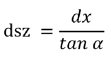
他方で、現在z方向に傾斜している距離dsは、


図13bでは、距離dxは、図13aにおけるのと同じ精度でもう一度測定することができる。しかしながら、次に、dx自体に含まれる任意の誤差、またはdxを測定する際に任意の誤差が、sinβ倍だけ減少させられる。それは、角度αを測定するまたは与える任意の決定/精度を保持する。したがって、図13bにおけるように断面像を傾斜させることによって、続く断面像間の距離を決定する精度全体が改善され得る。それは、垂直構造の場合、例えば、集積半導体サンプルに含まれるHARチャネルが位置決定に使用されることを保持する。ここで、重要な点は、サンプルの主軸に対して傾斜している平面からの位置情報を適用する何らかの位置決定が、サンプルの主軸に平行な平面からの位置情報を適用する位置決定よりも精度がよいことである。 In FIG. 13b, the distance dx can once again be measured with the same accuracy as in FIG. 13a. However, now any error contained in dx itself or in measuring dx is reduced by a factor of sinβ. It retains any determination/accuracy of measuring or giving the angle α. Thus, by tilting the cross-sectional images as in FIG. 13b, the overall accuracy of determining the distance between subsequent cross-sectional images can be improved. It retains that in the case of vertical structures, for example, HAR channels contained in an integrated semiconductor sample are used for position determination. The important point here is that any position determination that applies position information from a plane that is tilted with respect to the main axis of the sample is more accurate than a position determination that applies position information from a plane parallel to the main axis of the sample.
図14は、VNAND構造をイメージングするカーテニング効果の説明図である。ラインCが、断面像に見えており、これは、カーテニングによるアーチファクトである。カーテニングは、異なる材料が存在することにより生じる。カーテニングは、とても微細なVNAND構造を伴う場合である繰り返し構造がイメージングされる場合にとても顕著である。イメージング方法に応じて、カーテニングの強度は変わる。二次電子がイメージング信号として検出される場合、カーテニング効果は後方散乱電子が信号として検出される装置と比較してより強い。これは、二次電子が表面のトポグラフィにより敏感であり、トポグラフィのコントラストを結像する(image)ことによる。 Figure 14 is an illustration of the curtaining effect when imaging a VNAND structure. Line C is visible in the cross-sectional image, which is an artifact due to curtaining. Curtaining occurs due to the presence of different materials. Curtaining is very noticeable when repeating structures are imaged, which is the case with very fine VNAND structures. Depending on the imaging method, the strength of the curtaining varies. When secondary electrons are detected as the imaging signal, the curtaining effect is stronger compared to devices where backscattered electrons are detected as the signal. This is because secondary electrons are more sensitive to the surface topography and image the contrast of the topography.
しかしながら、後方散乱電子がイメージングのための信号として検出されるときも、像の情報は表面に対して様々な深さからやはり生じるので、カーテニングがさらに問題である。標準的な像再構成によって、後方散乱電子信号によって取得される断面像が平坦であると仮定される。しかしながら、これは、必ずしも正確にそうではない。この反駁は、像再構成における誤差をもたらし、仮想の像平面、例えば、数学的に再構成された像平面内の3D像の分解能を制限する。 However, when backscattered electrons are detected as a signal for imaging, curtaining is even more of a problem, since image information still originates from various depths relative to the surface. With standard image reconstruction, it is assumed that the cross-sectional image acquired with the backscattered electron signal is flat. However, this is not always exactly the case. This refutation introduces errors in the image reconstruction and limits the resolution of the 3D image in a virtual image plane, e.g., a mathematically reconstructed image plane.
したがって、本発明によれば、仮想像平面内の3D像の分解能は、カーテニング補正を実行することによって改善される。より詳細には、新しい断面のカーテニングシグネチャが決定される。図15は、表面の3Dトポグラフィを決定するそれぞれの配置を概略的に示す。イメージングデバイス90は、例えば電子を用いて働く、荷電粒子デバイスであり得る。示された例では、イメージングデバイス90は、SEMである。SEM90は、新しい断面の表面93をイメージングするものであり、集束イオンビームを用いて集積半導体サンプルをディレイヤリングすることから生じる。表面93は、平坦でなく、最大および最小を有する波状である。SEM90の走査方向は、示された例におけるx方向である。後方散乱電子を信号として検出する検出ユニットペアを構成する2つの検出ユニット95、96が用意されている。しかしながら、代替としてまたはさらに、表面93から発せられる二次電子がイメージングされることも可能である。検出ユニット95、96の幾何学的な配置は、それらが異なる角度の下で表面93から発する信号/粒子を検出するようになっている。しかしながら、示された実施形態では、2つの検出ユニット95、96の配置は、現在イメージングされている点またはエリアに対して対称的であり、(ここでは、電子ビーム軸の方向と同一の)表面93の法線に対する角度は、+/-δであり、検出ユニット95、96は、同じラインx上に、言い換えれば走査方向xに設けられる。しかしながら、他の角度および位置も可能である。
Thus, according to the invention, the resolution of the 3D image in the virtual image plane is improved by performing a curtaining correction. More specifically, a curtaining signature of the new cross section is determined. FIG. 15 shows a respective arrangement for determining the 3D topography of a surface in a schematic manner. The
SEM90を用いて最大94をイメージングするとき、検出ユニット95および96がその位置から発する粒子の形態で受信する信号強度は、トポグラフィによるシャドーイング効果のためにわずかに異なる。例えば、粒子が位置x1から発するとき、検出ユニット95は、検出ユニット92よりもよりわずかに強い信号を受信する。同様に、位置x2から発する粒子が検出されるとき、検出ユニット96の検出信号は、検出ユニット95における検出信号よりもわずかに強い。信号強度のこの差は、両検出ユニット95、96の差動信号において容易に解析することができる。したがって、例えば、ラインごとに表面93を走査することによって、表面93の3Dトポグラフィを決定することが可能である。したがって、表面93のカーテニングシグネチャが、決定され、断面像の再構成に使用されることができる。結果として得られる断面像は、それら自体3D像である。一例は、図16に示されている。図16の断面像は、波状3D構造を有する。定量的な3D情報は、増加した精度で3Dボリューム像の3D像再構成全体に使用することができる。代替としてまたはさらに、定量的な3D情報は、集積半導体サンプルの次の断面表面層を取り除く間に集束イオンビームを制御するフィードバックループに使用することができる。
When imaging the maximum 94 with the
図17は、VNANDメモリプローブにおける規則的な六角格子上の柱状構造の説明図である。VNANDメモリサンプルは、互いに平行に延びる多くの柱状構造で構成されている。本実施形態では、サンプルは、図18に示されるように「柱」に平行なスライスに切断される。図の像平面は、スライスに対して直角であり、フレーム領域として示された柱状フットプリント(pillar footprint)を含む。フットプリントの実際の形状は、円に近いことが期待される。フットプリントの図心は、規則的な(例えば、六角形の)格子を形成するように期待される。スライスに対して直角である方向に沿ったスライス位置の決定の不正確さ、および/または公称値からのスライス厚さの偏差は、この方向に沿った像スケールのドリフトをもたらす。結果として、柱断面は歪んで現れ(図の左部分参照)、その図心は、規則的な格子をそれ以上形成しない。 Figure 17 is an illustration of a columnar structure on a regular hexagonal lattice in a VNAND memory probe. A VNAND memory sample is composed of many columnar structures running parallel to each other. In this embodiment, the sample is cut into slices parallel to the "pillars" as shown in Figure 18. The image plane of the figure is perpendicular to the slices and contains the pillar footprints shown as frame regions. The actual shape of the footprint is expected to be close to a circle. The centroids of the footprints are expected to form a regular (e.g. hexagonal) lattice. Inaccuracies in the determination of the slice position along the direction perpendicular to the slices and/or deviations of the slice thickness from the nominal value will result in a drift of the image scale along this direction. As a result, the pillar cross sections appear distorted (see the left part of the figure) and their centroids no longer form a regular lattice.
本実施形態によれば、前述の歪みが最小化され、個々の柱の実際の幾何学的な特性を調査することを可能にするように、個々のスライス位置/厚さを調整することが提案される。この方法の概念は、例えば、設計データまたは(対称性のような)他の考慮事項から利用可能な柱状フットプリントの実際の形状および空間レイアウトについての情報を使用することである。例えば、実際の柱断面が平均して上述したように図心が規則的な六角格子を形成する完全な円(VNANDチップの大変ありふれた設計)であると仮定することは、十分であり得る。次いで、個々のスライスの位置/厚さが図18の右部分に示されるように、柱状フットプリントが仮定された幾何学的形状(規則的な格子上の円)に適合するまで調整される。任意の他のより複雑な柱状フットプリント形状、および/またはフットプリント図心の空間分布が、仮定されてもよい。さらに、説明した概念は、VNAND構造以外の他の構造に適用することもでき、構造の断面形状は、必ずしも丸または楕円ではない。 According to the present embodiment, it is proposed to adjust the individual slice positions/thicknesses in such a way that the aforementioned distortions are minimized, making it possible to investigate the actual geometric properties of the individual pillars. The idea of the method is to use information about the actual shape and spatial layout of the pillar footprint available, for example, from design data or other considerations (such as symmetry). For example, it may be sufficient to assume that the actual pillar cross-sections are on average perfect circles whose centroids form a regular hexagonal lattice as described above (a very common design of VNAND chips). The positions/thicknesses of the individual slices are then adjusted until the pillar footprint fits the assumed geometric shape (circle on a regular lattice), as shown in the right part of FIG. 18. Any other more complex pillar footprint shape and/or spatial distribution of footprint centroids may be assumed. Furthermore, the described concept can also be applied to other structures other than VNAND structures, the cross-sectional shape of the structure not necessarily being round or elliptical.
実際のプローブは設計からずれている場合がある、または特徴形状についての仮定が十分に正確ではない場合があるので、スライス位置調整後に取得した再構成された柱断面は、まだ実際のものからずれている可能性がある。しかしながら、ほとんどの場合は、設計からの柱の偏差を、むしろ局所的(欠陥!)であると予期する。例えば、ある柱は、その隣のものの柱から外れた形状または半径を有するかもしれない。また、その図心は、他の図心によって形成された規則的な格子上のそれぞれの位置からずれている可能性がある。そのような局所的な逸脱または欠陥は、スライス位置の説明した調整後にそのままであり、したがって調査され得る。実際、各スライスの調査された位置は、スライスによって「触れられた」全ての柱断面によって影響を受ける。調整されたスライス位置にある単一の柱断面の影響は、比較的小さいと予期される。すなわち、提案された調整は、局所的な欠陥を探すことを可能にする一方、不正確なスライス位置決定による像歪みをかなり減少させる。 The reconstructed column sections acquired after the slice position adjustment may still deviate from the real one, since the real probe may deviate from the design or the assumptions about the feature shapes may not be accurate enough. However, in most cases we expect the deviations of the columns from the design to be rather local (defects!). For example, a column may have a shape or radius that deviates from that of its neighbors. Also, its centroid may deviate from its respective position on the regular grid formed by the other centroids. Such local deviations or defects remain after the described adjustment of the slice position and can therefore be investigated. Indeed, the investigated position of each slice is influenced by all column sections "touched" by the slice. The influence of a single column section at the adjusted slice position is expected to be relatively small. That is, the proposed adjustment allows to look for local defects, while considerably reducing the image distortion due to inaccurate slice positioning.
概して、実際のスライスに対して直角である断面(または複数の断面)における知られているフットプリント形状および空間分布を有する特徴を含む任意のチップからのデータは、提案された方法で処理することができる。VNANDメモリチップレイアウトは、比較的小さい特徴フットプリントを伴う一例として使用されるものにすぎない。 In general, data from any chip containing features with known footprint shapes and spatial distribution in a cross section (or cross sections) that are perpendicular to the actual slice can be processed with the proposed method. The VNAND memory chip layout is used only as an example with relatively small feature footprints.
説明された方法は、スライス/断面像が小さい横方向オフセットに悩まされる場合にも拡張可能である。すなわち、スライスは、横方向のアライメントをさらに改善することができるようにスライス平面(断面像平面)に平行な方向に調整することもできる。 The described method is also extendable to cases where the slices/cross-sectional images suffer from small lateral offsets; i.e., the slices can also be adjusted in a direction parallel to the slice plane (cross-sectional image plane) so that the lateral alignment can be further improved.
図19は、図18のフットプリント形状ベースアライメントの詳細を概略的のさらに示す。X方向に沿った個々のスライスSの位置調整は、予期される形状の柱断面を含む参照像および予期される空間格子に基づく(図19のX方向は、他の図におけるX方向と同じではないが(z方向)、わずかに異なった専門語が、以下の理解を容易にするために選ばれていることに留意されたい)。 Figure 19 shows further schematic details of the footprint shape based alignment of Figure 18. The alignment of the individual slices S along the X direction is based on a reference image containing column cross sections of expected shape and the expected spatial grid (note that the X direction in Figure 19 is not the same as the X direction in the other figures (z direction), but slightly different nomenclature has been chosen to facilitate understanding of what follows).
提案されたスライス位置の調整についてのワークフローの特定の例は、以下のとおりである。柱状フットプリントの実際の形状(例えば、円)およびその空間分布(例えば、ある種の規則的な格子)についての利用可能な情報が、何ら歪みがないことが期待される柱(および実際のスライス)に直角である平面内で「参照像」Rを構成するために使用される。そのような参照像の一例が図19に示されている。この像における個々のスライスの断面は、Sで示されるY方向に沿った一次元ラインである。スライスSは、完全な格子上に位置するグレイで示された完全な円からなる参照像に適合するようにX方向に沿って調整される必要がある。参照像と全ての個々のスライスの両方が、柱状フットプリントに属する全てのピクセルが1に設定される一方、全ての他のピクセルがゼロに設定されるように二値化される。参照像Rのピクセルサイズは、個々のスライスSにおけるピクセルサイズに等しく設定される。XおよびY方向に沿ってピクセルの添え字iおよびkをそれぞれ導入することで、したがって、参照像は、二次元行列のR(i,k)=R(xi,yk)として表され得る。個々のスライス断面Sは、一次元ベクトルSk=S(yk)として表される。この方法の目標は、スライスSが参照像Rに最もよく適合するxiを見つけることである(図19参照)。そうするために、その公称位置まわりのスライスSについて可能なある範囲のX位置を試験することができる。この範囲からのxiごとに、メリット関数M(xi)の値が計算され、スライスSが位置xiで参照像Rにどのくらい良好に適合するのか特徴付ける。 A specific example of the workflow for the proposed slice position adjustment is as follows: The available information about the actual shape of the pillar footprint (e.g. a circle) and its spatial distribution (e.g. some kind of regular grid) is used to construct a "reference image" R in a plane perpendicular to the pillar (and the actual slices) that is expected to be free of any distortion. An example of such a reference image is shown in Fig. 19. The cross-section of the individual slices in this image is a one-dimensional line along the Y direction, denoted S. The slices S need to be adjusted along the X direction to fit the reference image, which consists of a perfect circle, denoted in grey, located on a perfect grid. Both the reference image and all individual slices are binarized such that all pixels belonging to the pillar footprint are set to 1, while all other pixels are set to zero. The pixel size of the reference image R is set equal to the pixel size in the individual slices S. By introducing pixel indices i and k along the X and Y directions, respectively, the reference image can therefore be represented as a two-dimensional matrix R (i,k) = R(x i , y k ). Each slice cross section S is represented as a one-dimensional vector Sk = S( yk ). The goal of the method is to find the x i where slice S best matches the reference image R (see FIG. 19). To do so, a range of possible X-positions for slice S around its nominal position can be tested. For each x i from this range, a value of the merit function M(x i ) is calculated, characterizing how well slice S matches the reference image R at position x i .

試験されたX-位置の範囲があまり大きくない(すなわち、初期のスライス位置決定の不確かさがあまり高くない)場合、Mは、個々のスライスSのための最終的な位置として使用され得るある位置xadjustedで固有の最小に到達する。説明された手順は、最終的に位置合わせされた(調整された)3Dスタックを取得するために個々のスライスSごとに繰り返すことができる。 If the range of X-positions tested is not too large (i.e., the uncertainty in the initial slice position determination is not too high), M reaches a unique minimum at some position x adjusted , which can be used as the final position for each slice S. The described procedure can be repeated for each individual slice S to obtain the final aligned (adjusted) 3D stack.
本実施形態の優れた精密アライメントは、本発明の各実施形態のいくつかの利点を考慮すると明らかになる。まず、金属ライン、ゲート、ビア、およびHARチャネルが、それぞれ、知られている平面内でおよび互いに知られている角度90°でそれぞれ延びており、任意の基準マークが製造できるよりもずっとより精巧な製造技法で製造される。半導体製造技術、例えば、液浸リソグラフィ露光、金属蒸着、またはイオン注入、方向付けられたRIEエッチング(directed RIE etching)、および集積回路のための研磨は、数nm、例えば7nm、5nm、または近い将来に3nmの臨界寸法に適応されM0などのゲート層および下側金属層などの最も下側および最も微細な層について、典型的なパターン配置またはオーバーレイ2nm未満の精度またはさらに1nm未満の精度になる。概して、金属ラインの精度全体が、最も短い寸法の金属ラインよりも約1/3倍よくなり、結果として、低い金属層およびゲート層のオーバーレイ精度は、1nm程度以下である。したがって、ゲートまたは金属ラインの位置精度または配置および寸法は、粗いFIBで支援された堆積プロセスによって製造される典型的な基準よりもずっと良く、ただし、FIBビーム径は例えば20nm程度であり、FIB走査位置精度は3~5nmを上回る。したがって、5nmまたは3nmなどの数nmの最小特徴サイズ(CD)を有する最近の集積半導体サンプルの金属ラインは、先行技術の基準ベースアライメントよりも少なくとも3倍改善される特徴ベースアライメントを可能にする。結果として、金属ラインまたはゲートについての図心の計算などの位置計算は、よりずっと高い精度をもたらし、断面像の変位は、基準の位置と比較してずっとより正確に決定され得る。画像処理技法を用いた金属ラインの抽出は、適宜、像歪みの評価および差し引きと組み合わされて、特徴または構造ベースレジストレーションによる断面像の改善された精密アライメントをそのようにもたらす。 The superior precision alignment of this embodiment becomes evident when considering several advantages of each embodiment of the present invention. First, the metal lines, gates, vias, and HAR channels each extend in a known plane and at a known angle of 90° to each other, and are manufactured with much more sophisticated manufacturing techniques than any fiducial marks can be manufactured. Semiconductor manufacturing techniques, such as immersion lithography exposure, metal deposition, or ion implantation, directed RIE etching, and polishing for integrated circuits, are adapted to critical dimensions of a few nm, e.g., 7 nm, 5 nm, or soon 3 nm, resulting in typical pattern placement or overlay accuracy of less than 2 nm or even less than 1 nm for the lowest and finest layers, such as gate layers and lower metal layers, such as M0. In general, the overall accuracy of the metal lines is about 1/3 times better than the metal lines of the shortest dimension, and as a result, the overlay accuracy of the lower metal layers and gate layers is on the order of 1 nm or less. Thus, the positional accuracy or placement and dimensions of the gate or metal line are much better than typical fiducials produced by coarse FIB-assisted deposition processes, although the FIB beam diameter is, for example, on the order of 20 nm, and the FIB scan positional accuracy is better than 3-5 nm. Thus, metal lines of modern integrated semiconductor samples with a minimum feature size (CD) of a few nm, such as 5 nm or 3 nm, allow feature-based alignment that is at least three times improved over prior art fiducial-based alignment. As a result, position calculations, such as centroid calculations, for metal lines or gates provide much higher accuracy, and the displacement of the cross-sectional image can be determined much more accurately compared to the position of the fiducial. Extraction of the metal line using image processing techniques, optionally combined with evaluation and subtraction of image distortions, thus provides improved precision alignment of the cross-sectional image by feature or structure-based registration.
第2に、断面像から、金属ライン、ビア、HARチャネル、またはゲートの位置が、例えば輪郭線から得られる。例えば、2つの続くスライスにおける単一の共通の特徴の図心の計算は、統計的平均化を含み、したがって例えば像のノイズに対してより頑健であり、それによって2つの像スライスのアライメントの精度を改善する。第3に、典型的なより多数Lの金属ライン、例えば2個、5個、10個、または100個までは、像レジストレーションおよびアライメントのために位置決定の統計結果をさらに改善する。ラインエッジラフネス導出は、少なくとも1.5倍だけ改善することができ、2~3倍が容易に実現され得る。欠陥は稀であるので、それらは一度に多くの構造を用いるアライメント方法の品質全体に影響を与えない。特徴ベースアライメント統計的評価は、したがって、先行技術の基準ベースアライメントよりも少なくとも1.5倍の改善を可能にすることが示される。 Secondly, from the cross-sectional image, the location of metal lines, vias, HAR channels or gates can be obtained, for example, from the contour lines. For example, the calculation of the centroid of a single common feature in two subsequent slices involves statistical averaging and is therefore more robust, for example, against image noise, thereby improving the accuracy of the alignment of the two image slices. Thirdly, a typical larger number L of metal lines, for example 2, 5, 10 or even 100, further improves the statistical results of the position determination for image registration and alignment. The line edge roughness derivation can be improved by at least a factor of 1.5, and a factor of 2-3 can be easily realized. Since defects are rare, they do not affect the overall quality of the alignment method using many structures at once. It is therefore shown that the feature-based alignment statistical evaluation allows for at least a factor of 1.5 improvement over the fiducial-based alignment of the prior art.
加えて、欠陥候補は、統計的評価から外れ値として検出することができる。 In addition, defect candidates can be detected as outliers from statistical evaluation.
別の実施形態では、または上述したものに加えて、集積半導体構造は、priory知られている構造である。設計情報または3DCAD情報は、金属ラインおよびHARチャネルのエッジ抽出、位置抽出、および像レジストレーションを改善するために使用することができる。例えば、CAD情報は、位置が金属ライン端であり、したがって断面像にもはや見えないはずであることを識別するのに使用され得る。それによって、画像処理方法の外れ値は、減じられ得る。加えて、欠陥候補は、統計的評価から外れ値として検出することができる。 In another embodiment, or in addition to those described above, the integrated semiconductor structure is a priori known structure. Design information or 3D CAD information can be used to improve edge extraction, position extraction, and image registration of the metal lines and HAR channels. For example, CAD information can be used to identify locations that are metal line ends and therefore should no longer be visible in the cross-sectional image. Thereby, outliers of the image processing method can be reduced. Additionally, defect candidates can be detected as outliers from the statistical evaluation.
別の実施形態では、構造または特徴ベースアライメントは、基準ベースアライメントと組み合わされる。集積半導体サンプルは、ゲート層内のゲートなどの非常に繰り返しの多い特徴を含み得、これは、像レジストレーションに不明瞭さをもたらし得る。概して、集積半導体サンプルの上部に形成された基準を用いる粗いレジストレーションは、本発明の実施形態のいずれかによる特徴または構造ベースアライメントによって、不明瞭さを減少させ、微細像レジストレーションの速度を増加させることができる。 In another embodiment, structure or feature based alignment is combined with fiducial based alignment. Integrated semiconductor samples may contain highly repetitive features, such as gates in a gate layer, which may introduce ambiguities in image registration. In general, coarse registration using fiducials formed on top of the integrated semiconductor sample can reduce ambiguities and increase the speed of fine image registration with feature or structure based alignment according to any of the embodiments of the present invention.
コーナまたはエッジ検出、閾値処理、もしくはモフォロジー処理、または類似する演算などの上述したような画像処理方法は、当業界でよく知られている。画像処理は、例えば、数100個のプロセッサを含むコンピュータクラスタの使用によって、計算速度の向上によって近頃改善されている。集積半導体サンプルの特徴または構造を抽出する画像処理方法は、機械学習アルゴリズムを含むこともでき、または機械学習アルゴリズムによって置き換えることもできる。 Image processing methods such as those mentioned above, such as corner or edge detection, thresholding, or morphological processing, or similar operations, are well known in the art. Image processing has recently been improved by increasing computation speed, for example by the use of computer clusters containing hundreds of processors. Image processing methods for extracting features or structures of integrated semiconductor samples may include or be replaced by machine learning algorithms.
上述した実施形態は、単に例であることが意図されている。実施形態がプローブとして半導体構造の例に記載されているにも関わらず、本方法は、精密な像レジストレーションを可能にする同等の構造の材料またはプローブに同様に適用され得る。改変、修正、変更、および組合せが、本明細書に添付された特許請求の範囲によって定められる範囲から逸脱することなく、当業者によって特定の実施形態にもたらされてもよい。 The above-described embodiments are intended to be examples only. Although the embodiments are described in the example of a semiconductor structure as a probe, the method may be similarly applied to materials or probes of comparable structure that allow for precise image registration. Alterations, modifications, variations, and combinations may be effected in the particular embodiments by those skilled in the art without departing from the scope defined by the claims appended hereto.
参照符号のリスト
番号 項目
10 サンプル
11 断面表面
20 表面堆積材料
21 第1の基準マーカー
22 第2の基準マーカー
25 第1の基準マーカーの断面像セグメント
27 第2の基準マーカーの断面像セグメント
50 FIB柱
51 集束イオン粒子ビーム
52 第1の断面表面
53 第2の断面表面
54 第3の断面表面
55 サンプル上面
61 z方向に延びた第1の金属ライン
62.1、62.2 x方向に延びた第2の金属ライン
63 第2の金属ラインの断面
64 第1の金属ラインの断面
65 ビアの断面
66 金属ラインの断面像セグメントの境界線
67 金属ラインの断面像セグメントの図心
68 z方向を通る層M1における金属ラインの断面像セグメントの図心のトレース
69 z方向を通る層M7における金属ラインの断面像セグメントの図心のトレース
71 断面像に対して直角であるz方向と所定の角度をなす方向に細長い第1の金属ライン
72 断面像に対して直角であるz方向と第2の角度をなす方向に細長い第2の金属ライン
73.1、73.2 第1の金属ライン71の断面像セグメント
74.1、74.2 第2の金属ライン72の断面像セグメント
75 上面55に対して直角であるHARチャネルまたは金属ライン
77.1、77.2 上面に対して直角であるHARチャネルまたは金属ラインの断面像セグメント
91 基準ベースアライメント後の金属ラインのラインエッジ
92 特徴ベースアライメント後の金属ラインのラインエッジ
93 断面の波状面
94 トポグラフィの最大
95 第1の検出ユニット
96 第2の検出ユニット
100、100.1、100.2、100.3 断面像
101 z方向の延びた金属ライン
102 x方向に延びた金属ライン
110 第1の断面像
111 第2の断面像
210 第1の断面像
211 第2の断面像
300 像歪みベクトル
301 像歪みベクトルの外れ値
302 断面像内の金属ラインの断面像セグメントの図心
1000 一連の断面像
±δ 表面法線と検出ユニットの間の角度
LIST OF REFERENCE NUMBERS Item 10 Sample 11 Cross-sectional surface 20 Surface deposited material 21 First fiducial marker 22 Second fiducial marker 25 Cross-sectional image segment of first fiducial marker 27 Cross-sectional image segment of second fiducial marker 50 FIB column 51 Focused ion particle beam 52 First cross-sectional surface 53 Second cross-sectional surface 54 Third cross-sectional surface 55 Sample top surface 61 First metal line 62.1, 62.2 extending in the z-direction Second metal line 63 Cross-section of second metal line 64 Cross-section of first metal line 65 Cross-section of via 66 Boundary of cross-sectional image segment of metal line 67 Centroid of cross-sectional image segment of metal line 68 Trace of centroid of cross-sectional image segment of metal line in layer M1 through the z-direction 69 Trace of centroid of cross-sectional image segment of metal line in layer M7 through the z-direction 71 A first metal line 72 elongated in a direction forming an angle with the z-direction perpendicular to the cross-sectional image A second metal line 73.1, 73.2 elongated in a direction forming a second angle with the z-direction perpendicular to the cross-sectional image Cross-sectional image segments 74.1, 74.2 of the first metal line 71 Cross-sectional image segments 75 of the second metal line 72 HAR channels or metal lines 77.1, 77.2 perpendicular to the top surface 55 Cross-sectional image segments 91 of the HAR channels or metal lines perpendicular to the top surface Line edges 92 of the metal lines after fiducial-based alignment Line edges 93 of the metal lines after feature-based alignment Wavy surface of the cross-section 94 Maximum of the topography 95 First detection unit 96 Second detection unit 100, 100.1, 100.2, 100.3 Cross-sectional image 101 Metal lines extending in the z-direction 102 Metal lines extending in the x-direction 110 First cross-sectional image 111 Second cross-sectional image 210 First cross-sectional image 211 Second cross-sectional image 300 Image distortion vector 301 Image distortion vector outlier 302 Centroid 1000 of cross-sectional image segment of metal line in cross-sectional image Series of cross-sectional images ±δ Angle between surface normal and detection unit
Claims (31)
- 繰り返される表面層の取り除き及び断面イメージングにより一連の2D断面像を取得するステップであって、前記一連の2D断面像は、少なくとも第1の断面像および前記第1の断面像に平行な第2の断面像を含み、
前記一連の2D断面像を取得するステップは、
イメージングのためにアクセス可能な第1の新しい断面を作製するように集束イオンビームを用いて前記集積半導体サンプルの断面表面層を取り除くステップ、
イメージングデバイスを用いて前記集積半導体サンプルの前記第1の新しい断面をイメージングし、それによって前記第1の断面像を取得するステップ、
イメージングのためにアクセス可能な第2の新しい断面を作製するように集束イオンビームを用いて次の断面表面層を取り除くステップ、および、
前記イメージングデバイスを用いて前記集積半導体サンプルの前記第2の新しい断面をイメージングし、それによって前記第2の断面像を取得するステップ、
を含む、取得するステップと、
- 前記少なくとも第1および第2の断面像の各々の像レジストレーションによって前記少なくとも第1および第2の断面像の特徴ベースアライメントを取得するステップであって、
前記像レジストレーションは、前記少なくとも第1および第2の断面像における前記集積半導体サンプルの少なくとも1つの共通の特徴に基づいて実行される、取得するステップと、
を特徴とし、
前記像レジストレーション後に、前記少なくとも第1および第2の断面像は、3Dボリューム像と組み合わされ、
前記少なくとも第1および第2の断面像は、前記集積半導体サンプルの上面に対して傾斜して形成され、前記少なくとも第1の断面像と第2の断面像の間の距離は、前記上面に設けられた基準の位置に基づいて決定される、
方法。 1. A method for acquiring a 3D volumetric image of an integrated semiconductor sample by alignment based on features of the integrated semiconductor sample, comprising:
- obtaining a series of 2D cross-sectional images by repeated removal of the surface layer and cross-sectional imaging, said series of 2D cross-sectional images comprising at least a first cross-sectional image and a second cross-sectional image parallel to said first cross-sectional image;
The step of acquiring the series of 2D cross-sectional images comprises:
removing a cross-sectional surface layer of the integrated semiconductor sample using a focused ion beam to create a first new cross-section accessible for imaging;
imaging the first new cross-section of the integrated semiconductor sample with an imaging device, thereby obtaining the first cross-sectional image;
removing a next cross-sectional surface layer using a focused ion beam to create a second new cross-section accessible for imaging; and
imaging the second new cross-section of the integrated semiconductor sample with the imaging device, thereby obtaining the second cross-sectional image;
obtaining the image ;
obtaining a feature-based alignment of said at least first and second cross-sectional images by image registration of each of said at least first and second cross-sectional images,
the image registration is performed based on at least one common feature of the integrated semiconductor sample in the at least first and second cross-sectional images;
It is characterized by:
After said image registration, said at least first and second cross-sectional images are combined with a 3D volume image ;
the at least first and second cross-sectional images are formed at an angle with respect to a top surface of the integrated semiconductor sample, and a distance between the at least first and second cross-sectional images is determined based on a position of a reference provided on the top surface.
method.
- 繰り返される表面層の取り除き及び断面イメージングにより一連の2D断面像を取得するステップであって、前記一連の2D断面像は、少なくとも第1の断面像および前記第1の断面像に平行な第2の断面像を含み、
前記一連の2D断面像を取得するステップは、
イメージングのためにアクセス可能な第1の新しい断面を作製するように集束イオンビームを用いて前記集積半導体サンプルの断面表面層を取り除くステップ、
イメージングデバイスを用いて前記集積半導体サンプルの前記第1の新しい断面をイメージングし、それによって前記第1の断面像を取得するステップ、
イメージングのためにアクセス可能な第2の新しい断面を作製するように集束イオンビームを用いて次の断面表面層を取り除くステップ、および、
前記イメージングデバイスを用いて前記集積半導体サンプルの前記第2の新しい断面をイメージングし、それによって前記第2の断面像を取得するステップ、
を含む、取得するステップと、
- 前記少なくとも第1および第2の断面像の各々の像レジストレーションによって前記少なくとも第1および第2の断面像の特徴ベースアライメントを取得するステップであって、
前記像レジストレーションは、前記少なくとも第1および第2の断面像における前記集積半導体サンプルの少なくとも1つの共通の特徴に基づいて実行される、取得するステップと、
を特徴とし、
前記像レジストレーション後に、前記少なくとも第1および第2の断面像は、3Dボリューム像と組み合わされ、
前記方法は、前記特徴ベースアライメントに先だってアライメントマークの位置を測定および評価することによって前記少なくとも第1および第2の断面像の基準ベースアライメントを用意することを含む、
方法。 1. A method for acquiring a 3D volumetric image of an integrated semiconductor sample by alignment based on features of the integrated semiconductor sample, comprising:
- obtaining a series of 2D cross-sectional images by repeated removal of the surface layer and cross-sectional imaging, said series of 2D cross-sectional images comprising at least a first cross-sectional image and a second cross-sectional image parallel to said first cross-sectional image;
The step of acquiring the series of 2D cross-sectional images comprises:
removing a cross-sectional surface layer of the integrated semiconductor sample using a focused ion beam to create a first new cross-section accessible for imaging;
imaging the first new cross-section of the integrated semiconductor sample with an imaging device, thereby obtaining the first cross-sectional image;
removing a next cross-sectional surface layer using a focused ion beam to create a second new cross-section accessible for imaging; and
imaging the second new cross-section of the integrated semiconductor sample with the imaging device, thereby obtaining the second cross-sectional image;
obtaining the signal;
obtaining a feature-based alignment of said at least first and second cross-sectional images by image registration of each of said at least first and second cross-sectional images,
the image registration is performed based on at least one common feature of the integrated semiconductor sample in the at least first and second cross-sectional images;
It is characterized by:
After said image registration, said at least first and second cross-sectional images are combined with a 3D volume image;
the method including providing a fiducial-based alignment of the at least first and second cross-sectional images by measuring and evaluating positions of alignment marks prior to the feature-based alignment;
method.
- 繰り返される表面層の取り除き及び断面イメージングにより一連の2D断面像を取得するステップであって、前記一連の2D断面像は、少なくとも第1の断面像および前記第1の断面像に平行な第2の断面像を含み、
前記一連の2D断面像を取得するステップは、
イメージングのためにアクセス可能な第1の新しい断面を作製するように集束イオンビームを用いて前記集積半導体サンプルの断面表面層を取り除くステップ、
イメージングデバイスを用いて前記集積半導体サンプルの前記第1の新しい断面をイメージングし、それによって前記第1の断面像を取得するステップ、
イメージングのためにアクセス可能な第2の新しい断面を作製するように集束イオンビームを用いて次の断面表面層を取り除くステップ、および、
前記イメージングデバイスを用いて前記集積半導体サンプルの前記第2の新しい断面をイメージングし、それによって前記第2の断面像を取得するステップ、
を含む、取得するステップと、
- 前記少なくとも第1および第2の断面像の各々の像レジストレーションによって前記少なくとも第1および第2の断面像の特徴ベースアライメントを取得するステップであって、
前記像レジストレーションは、前記少なくとも第1および第2の断面像における前記集積半導体サンプルの少なくとも1つの共通の特徴に基づいて実行される、取得するステップと、
を特徴とし、
前記像レジストレーション後に、前記少なくとも第1および第2の断面像は、3Dボリューム像と組み合わされ、
前記少なくとも第1および第2の断面像は、前記集積半導体サンプルの上面に対して傾斜して形成され、前記少なくとも第1の断面像と第2の断面像の間の距離は、特徴の位置に基づいて決定される、
方法。 1. A method for acquiring a 3D volumetric image of an integrated semiconductor sample by alignment based on features of the integrated semiconductor sample, comprising:
- obtaining a series of 2D cross-sectional images by repeated removal of the surface layer and cross-sectional imaging, said series of 2D cross-sectional images comprising at least a first cross-sectional image and a second cross-sectional image parallel to said first cross-sectional image;
The step of acquiring the series of 2D cross-sectional images comprises:
removing a cross-sectional surface layer of the integrated semiconductor sample using a focused ion beam to create a first new cross-section accessible for imaging;
imaging the first new cross-section of the integrated semiconductor sample with an imaging device, thereby obtaining the first cross-sectional image;
removing a next cross-sectional surface layer using a focused ion beam to create a second new cross-section accessible for imaging; and
imaging the second new cross-section of the integrated semiconductor sample with the imaging device, thereby obtaining the second cross-sectional image;
obtaining the signal;
obtaining a feature-based alignment of said at least first and second cross-sectional images by image registration of each of said at least first and second cross-sectional images,
the image registration is performed based on at least one common feature of the integrated semiconductor sample in the at least first and second cross-sectional images;
It is characterized by:
After said image registration, said at least first and second cross-sectional images are combined with a 3D volume image;
the at least first and second cross-sectional images are formed at an angle relative to a top surface of the integrated semiconductor sample, and a distance between the at least first and second cross-sectional images is determined based on a location of a feature .
method.
- 繰り返される表面層の取り除き及び断面イメージングにより一連の2D断面像を取得するステップであって、前記一連の2D断面像は、少なくとも第1の断面像および前記第1の断面像に平行な第2の断面像を含み、
前記一連の2D断面像を取得するステップは、
イメージングのためにアクセス可能な第1の新しい断面を作製するように集束イオンビームを用いて前記集積半導体サンプルの断面表面層を取り除くステップ、
イメージングデバイスを用いて前記集積半導体サンプルの前記第1の新しい断面をイメージングし、それによって前記第1の断面像を取得するステップ、
イメージングのためにアクセス可能な第2の新しい断面を作製するように集束イオンビームを用いて次の断面表面層を取り除くステップ、および、
前記イメージングデバイスを用いて前記集積半導体サンプルの前記第2の新しい断面をイメージングし、それによって前記第2の断面像を取得するステップ、
を含む、取得するステップと、
- 前記少なくとも第1および第2の断面像の各々の像レジストレーションによって前記少なくとも第1および第2の断面像の特徴ベースアライメントを取得するステップであって、
前記像レジストレーションは、前記少なくとも第1および第2の断面像における前記集積半導体サンプルの少なくとも1つの共通の特徴に基づいて実行される、取得するステップと、
を特徴とし、
前記像レジストレーション後に、前記少なくとも第1および第2の断面像は、3Dボリューム像と組み合わされ、
前記特徴ベースアライメントは、前記少なくとも第1の断面像と第2の断面像の間の像歪み偏差の差し引きを含む、
方法。 1. A method for acquiring a 3D volumetric image of an integrated semiconductor sample by alignment based on features of the integrated semiconductor sample, comprising:
- obtaining a series of 2D cross-sectional images by repeated removal of the surface layer and cross-sectional imaging, said series of 2D cross-sectional images comprising at least a first cross-sectional image and a second cross-sectional image parallel to said first cross-sectional image;
The step of acquiring the series of 2D cross-sectional images comprises:
removing a cross-sectional surface layer of the integrated semiconductor sample using a focused ion beam to create a first new cross-section accessible for imaging;
imaging the first new cross-section of the integrated semiconductor sample with an imaging device, thereby obtaining the first cross-sectional image;
removing a next cross-sectional surface layer using a focused ion beam to create a second new cross-section accessible for imaging; and
imaging the second new cross-section of the integrated semiconductor sample with the imaging device, thereby obtaining the second cross-sectional image;
obtaining the image;
obtaining a feature-based alignment of said at least first and second cross-sectional images by image registration of each of said at least first and second cross-sectional images,
the image registration is performed based on at least one common feature of the integrated semiconductor sample in the at least first and second cross-sectional images;
It is characterized by:
After said image registration, said at least first and second cross-sectional images are combined with a 3D volume image;
the feature-based alignment includes subtracting image distortion deviations between the at least first cross-sectional image and the at least second cross-sectional image.
method.
- 繰り返される表面層の取り除き及び断面イメージングにより一連の2D断面像を取得するステップであって、前記一連の2D断面像は、少なくとも第1の断面像および前記第1の断面像に平行な第2の断面像を含み、
前記一連の2D断面像を取得するステップは、
イメージングのためにアクセス可能な第1の新しい断面を作製するように集束イオンビームを用いて前記集積半導体サンプルの断面表面層を取り除くステップ、
イメージングデバイスを用いて前記集積半導体サンプルの前記第1の新しい断面をイメージングし、それによって前記第1の断面像を取得するステップ、
イメージングのためにアクセス可能な第2の新しい断面を作製するように集束イオンビームを用いて次の断面表面層を取り除くステップ、および、
前記イメージングデバイスを用いて前記集積半導体サンプルの前記第2の新しい断面をイメージングし、それによって前記第2の断面像を取得するステップ、
を含む、取得するステップと、
- 前記少なくとも第1および第2の断面像の各々の像レジストレーションによって前記少なくとも第1および第2の断面像の特徴ベースアライメントを取得するステップであって、
前記像レジストレーションは、前記少なくとも第1および第2の断面像における前記集積半導体サンプルの少なくとも1つの共通の特徴に基づいて実行される、取得するステップと、
を特徴とし、
前記像レジストレーション後に、前記少なくとも第1および第2の断面像は、3Dボリューム像と組み合わされ、
前記方法は、
前記新しい断面のカーテニングシグネチャを決定するステップと、
3D断面像として前記断面像を表すために前記カーテニングシグネチャを使用するステップと
を含む、
方法。 1. A method for acquiring a 3D volumetric image of an integrated semiconductor sample by alignment based on features of the integrated semiconductor sample, comprising:
- obtaining a series of 2D cross-sectional images by repeated removal of the surface layer and cross-sectional imaging, said series of 2D cross-sectional images comprising at least a first cross-sectional image and a second cross-sectional image parallel to said first cross-sectional image;
The step of acquiring the series of 2D cross-sectional images comprises:
removing a cross-sectional surface layer of the integrated semiconductor sample using a focused ion beam to create a first new cross-section accessible for imaging;
imaging the first new cross-section of the integrated semiconductor sample with an imaging device, thereby obtaining the first cross-sectional image;
removing a next cross-sectional surface layer using a focused ion beam to create a second new cross-section accessible for imaging; and
imaging the second new cross-section of the integrated semiconductor sample with the imaging device, thereby obtaining the second cross-sectional image;
obtaining the image;
obtaining a feature-based alignment of said at least first and second cross-sectional images by image registration of each of said at least first and second cross-sectional images,
the image registration is performed based on at least one common feature of the integrated semiconductor sample in the at least first and second cross-sectional images;
It is characterized by:
After said image registration, said at least first and second cross-sectional images are combined with a 3D volume image;
The method comprises:
determining a curtaining signature of the new cross section;
and using the curtaining signature to represent the cross-sectional image as a 3D cross-sectional image.
method.
- 繰り返される表面層の取り除き及び断面イメージングにより一連の2D断面像を取得するステップであって、前記一連の2D断面像は、少なくとも第1の断面像および前記第1の断面像に平行な第2の断面像を含み、
前記一連の2D断面像を取得するステップは、
イメージングのためにアクセス可能な第1の新しい断面を作製するように集束イオンビームを用いて前記集積半導体サンプルの断面表面層を取り除くステップ、
イメージングデバイスを用いて前記集積半導体サンプルの前記第1の新しい断面をイメージングし、それによって前記第1の断面像を取得するステップ、
イメージングのためにアクセス可能な第2の新しい断面を作製するように集束イオンビームを用いて次の断面表面層を取り除くステップ、および、
前記イメージングデバイスを用いて前記集積半導体サンプルの前記第2の新しい断面をイメージングし、それによって前記第2の断面像を取得するステップ、
を含む、取得するステップと、
- 前記少なくとも第1および第2の断面像の各々の像レジストレーションによって前記少なくとも第1および第2の断面像の特徴ベースアライメントを取得するステップであって、
前記像レジストレーションは、前記少なくとも第1および第2の断面像における前記集積半導体サンプルの少なくとも1つの共通の特徴に基づいて実行される、取得するステップと、
を特徴とし、
前記像レジストレーション後に、前記少なくとも第1および第2の断面像は、3Dボリューム像と組み合わされ、
前記方法は、
前記新しい断面のカーテニングシグネチャを決定するステップと、
前記集積半導体サンプルの次の断面表面層を取り除く間に前記集束イオンビームを制御するためにフィードバックループ内で前記決定されたカーテニングシグネチャを使用するステップと
を含む、
方法。 1. A method for acquiring a 3D volumetric image of an integrated semiconductor sample by alignment based on features of the integrated semiconductor sample, comprising:
- obtaining a series of 2D cross-sectional images by repeated removal of the surface layer and cross-sectional imaging, said series of 2D cross-sectional images comprising at least a first cross-sectional image and a second cross-sectional image parallel to said first cross-sectional image;
The step of acquiring the series of 2D cross-sectional images comprises:
removing a cross-sectional surface layer of the integrated semiconductor sample using a focused ion beam to create a first new cross-section accessible for imaging;
imaging the first new cross-section of the integrated semiconductor sample with an imaging device, thereby obtaining the first cross-sectional image;
removing a next cross-sectional surface layer using a focused ion beam to create a second new cross-section accessible for imaging; and
imaging the second new cross-section of the integrated semiconductor sample with the imaging device, thereby obtaining the second cross-sectional image;
obtaining the signal;
obtaining a feature-based alignment of said at least first and second cross-sectional images by image registration of each of said at least first and second cross-sectional images,
the image registration is performed based on at least one common feature of the integrated semiconductor sample in the at least first and second cross-sectional images;
It is characterized by:
After said image registration, said at least first and second cross-sectional images are combined with a 3D volume image;
The method comprises:
determining a curtaining signature of the new cross section;
and using the determined curtaining signature in a feedback loop to control the focused ion beam during removal of a next cross-sectional surface layer of the integrated semiconductor sample.
method.
電子で動作するとともに、前記集積半導体サンプルの前記新しい断面をイメージングするように適合された荷電粒子操作デバイスと、備え、
前記集束イオンビームおよび電子ビームは互いに対してある角度で配置および動作され、前記集束イオンビームのビーム軸およびビーム軸の電子ビームは互いに交差する、
請求項22に記載の半導体検査デバイス。 A focused ion beam device;
a charged particle manipulation device adapted to operate with electrons and to image the new cross-section of the integrated semiconductor sample;
the focused ion beam and the electron beam are positioned and moved at an angle to each other, and the beam axis of the focused ion beam and the beam axis of the electron beam intersect each other;
23. The semiconductor inspection device of claim 22 .
前記集束イオンビームおよび電子ビームは、互いに約90°の角度をなす、
請求項22に記載の半導体検査デバイス。 a beam axis of the focused ion beam and a top surface of the integrated semiconductor sample are at an angle of about 90° to each other;
The focused ion beam and the electron beam are at an angle of about 90° to each other.
23. The semiconductor inspection device of claim 22 .
前記集束イオンビームおよび電子ビームは、互いに約90°の角度をなす、
請求項22に記載の半導体検査デバイス。 a beam axis of the focused ion beam and a top surface of the integrated semiconductor sample are at an angle of about 25° to each other;
The focused ion beam and the electron beam are at an angle of about 90° to each other.
23. The semiconductor inspection device of claim 22 .
前記方法は、
- 繰り返される表面層の取り除き及び断面イメージングにより一連の2D断面像を取得するステップであって、前記一連の2D断面像は、少なくとも第1の断面像および前記第1の断面像に平行な第2の断面像を含み、
前記一連の2D断面像を取得するステップは、
イメージングのためにアクセス可能な第1の新しい断面を作製するように集束イオンビームを用いて前記集積半導体サンプルの断面表面層を取り除くステップ、
イメージングデバイスを用いて前記集積半導体サンプルの前記第1の新しい断面をイメージングし、それによって前記第1の断面像を取得するステップ、
イメージングのためにアクセス可能な第2の新しい断面を作製するように集束イオンビームを用いて次の断面表面層を取り除くステップ、および、
前記イメージングデバイスを用いて前記集積半導体サンプルの前記第2の新しい断面をイメージングし、それによって前記第2の断面像を取得するステップ、
を含む、取得するステップと、
- 前記少なくとも第1および第2の断面像の各々の像レジストレーションによって前記少なくとも第1および第2の断面像の特徴ベースアライメントを取得するステップであって、
前記像レジストレーションは、前記少なくとも第1および第2の断面像における前記集積半導体サンプルの少なくとも1つの共通の特徴に基づいて実行される、取得するステップと、
を特徴とし、
前記像レジストレーション後に、前記少なくとも第1および第2の断面像は、3Dボリューム像と組み合わされる、
半導体検査デバイス。 1. A semiconductor inspection device adapted to perform a method for acquiring a 3D volumetric image of an integrated semiconductor sample by alignment based on features of the integrated semiconductor sample, wherein an imaging device for imaging a new cross-section of the integrated semiconductor sample comprises at least two detection units arranged at different positions for detecting particles emanating from the new cross-section at different angles ,
The method comprises:
- obtaining a series of 2D cross-sectional images by repeated removal of the surface layer and cross-sectional imaging, said series of 2D cross-sectional images comprising at least a first cross-sectional image and a second cross-sectional image parallel to said first cross-sectional image;
The step of acquiring the series of 2D cross-sectional images comprises:
removing a cross-sectional surface layer of the integrated semiconductor sample using a focused ion beam to create a first new cross-section accessible for imaging;
imaging the first new cross-section of the integrated semiconductor sample with an imaging device, thereby obtaining the first cross-sectional image;
removing a next cross-sectional surface layer using a focused ion beam to create a second new cross-section accessible for imaging; and
imaging the second new cross-section of the integrated semiconductor sample with the imaging device, thereby obtaining the second cross-sectional image;
obtaining the signal;
obtaining a feature-based alignment of said at least first and second cross-sectional images by image registration of each of said at least first and second cross-sectional images,
the image registration is performed based on at least one common feature of the integrated semiconductor sample in the at least first and second cross-sectional images;
It is characterized by:
After the image registration, the at least first and second cross-sectional images are combined with a 3D volume image.
Semiconductor inspection devices.
- 一連のN個の断面像を取得するステップであって、
前記一連のN個の断面像を取得するステップは、続いて、イメージングのためにアクセス可能な新しい断面を作製するように集束イオンビームを用いて前記集積半導体サンプルの断面表面層を取り除くステップ、および荷電粒子イメージングデバイスを用いて前記集積半導体サンプルの前記新しい断面をイメージングするステップを含み、
前記一連のN個の断面像の各断面像平面は、z方向に対して直角に向けられ、前記集積半導体サンプルは、前記集積半導体サンプルの少なくとも1つの金属層MkのL個の金属ラインのセットに平行な方向が断面像平面に対してある角度をなすように配置され、
前記一連のN個の断面像の少なくともサブセットは、前記L個の金属ラインの断面像セグメントを含む、一連のN個の断面像を取得するステップと、
- 前記l=1~Lの金属ラインの前記断面像セグメントごとの位置P(x,y;l)を抽出するステップと、
- 前記一連のN個の断面像の少なくともサブセットの前記z方向を通る前記位置P(x,y;l)のトレースT(x,y;z;l)を形成するステップと、
- 前記トレースT(x,y;z;l)を平均的な共通の波状構造TA(x,y;z)および残留偏差dT(x,y;z;l)に分解するステップと、
- 前記共通の波状構造TA(x,y;z)を用いて前記一連のN個の断面像の前記サブセットを変位させることによって前記3Dボリューム像内の前記一連のN個の断面像の少なくとも前記サブセットの前記位置を補正するステップと、を特徴とする方法。 1. A method for acquiring a 3D volumetric image of an integrated semiconductor sample, comprising:
- acquiring a series of N cross-sectional images,
obtaining the series of N cross-sectional images subsequently includes removing a cross-sectional surface layer of the integrated semiconductor sample using a focused ion beam to create a new cross-section accessible for imaging, and imaging the new cross-section of the integrated semiconductor sample using a charged particle imaging device;
each cross-sectional image plane of the series of N cross-sectional images is oriented perpendicular to the z-direction, and the integrated semiconductor sample is positioned such that a direction parallel to a set of L metal lines of at least one metal layer Mk of the integrated semiconductor sample is at an angle to the cross-sectional image plane;
acquiring a series of N cross-sectional images, at least a subset of the series of N cross-sectional images including cross-sectional image segments of the L metal lines;
extracting the positions P(x,y;l) of each of said cross-sectional image segments of said metal lines l=1 to L;
forming a trace T(x,y;z;l) of said positions P(x,y;l) through said z direction of at least a subset of said series of N cross-sectional images;
- decomposing said trace T(x,y;z;l) into an average common wave structure TA(x,y;z) and a residual deviation dT(x,y;z;l);
- correcting the position of at least the subset of the series of N cross-sectional images within the 3D volume image by displacing the subset of the series of N cross-sectional images using the common wave-like structure TA(x, y; z).
Applications Claiming Priority (5)
| Application Number | Priority Date | Filing Date | Title |
|---|---|---|---|
| US201962858470P | 2019-06-07 | 2019-06-07 | |
| US62/858,470 | 2019-06-07 | ||
| DE102019006645.6 | 2019-09-20 | ||
| DE102019006645 | 2019-09-20 | ||
| PCT/EP2020/000101 WO2020244795A1 (en) | 2019-06-07 | 2020-05-25 | Cross section imaging with improved 3d volume image reconstruction accuracy |
Publications (2)
| Publication Number | Publication Date |
|---|---|
| JP2022535601A JP2022535601A (en) | 2022-08-09 |
| JP7546001B2 true JP7546001B2 (en) | 2024-09-05 |
Family
ID=71083570
Family Applications (1)
| Application Number | Title | Priority Date | Filing Date |
|---|---|---|---|
| JP2021572837A Active JP7546001B2 (en) | 2019-06-07 | 2020-05-25 | Cross-sectional imaging with improved 3D volumetric image reconstruction accuracy - Patents.com |
Country Status (7)
| Country | Link |
|---|---|
| US (1) | US20220138973A1 (en) |
| EP (1) | EP3980970A1 (en) |
| JP (1) | JP7546001B2 (en) |
| KR (1) | KR20220082802A (en) |
| CN (1) | CN113950704B (en) |
| TW (1) | TWI776163B (en) |
| WO (1) | WO2020244795A1 (en) |
Families Citing this family (32)
| Publication number | Priority date | Publication date | Assignee | Title |
|---|---|---|---|---|
| JP7719089B2 (en) | 2020-03-13 | 2025-08-05 | カール・ツァイス・エスエムティー・ゲーエムベーハー | Method for cross-sectional imaging of an inspection volume in a wafer |
| CN114689630B (en) * | 2020-12-30 | 2025-12-02 | Fei公司 | Methods and systems for imaging three-dimensional features |
| TWI812091B (en) * | 2021-04-21 | 2023-08-11 | 德商卡爾蔡司Smt有限公司 | Methods of training a machine-learning logic and analyzing rings of pillar cross sections in high aspect ratio structures, semiconductor inspection devices, computer program, and tangible storage medium |
| US11728126B2 (en) | 2021-06-24 | 2023-08-15 | Applied Materials Israel Ltd. | 3D metrology from 3D datacube created from stack of registered images obtained during delayering of the sample |
| WO2023004294A1 (en) * | 2021-07-19 | 2023-01-26 | Onto Innovation Inc. | Low contrast non-referential defect detection |
| EP4148765A1 (en) * | 2021-09-08 | 2023-03-15 | ASML Netherlands B.V. | Sem image enhancement |
| US12056865B2 (en) * | 2021-10-07 | 2024-08-06 | Carl Zeiss Smt Gmbh | Wafer-tilt determination for slice-and-image process |
| US12159394B2 (en) | 2021-11-04 | 2024-12-03 | Saudi Arabian Oil Company | System and method for orienting geological core samples |
| US11848172B2 (en) * | 2021-11-09 | 2023-12-19 | Carl Zeiss Smt Gmbh | Method for measuring a sample and microscope implementing the method |
| WO2023117238A1 (en) | 2021-12-20 | 2023-06-29 | Carl Zeiss Smt Gmbh | Measurement method and apparatus for semiconductor features with increased throughput |
| US20230196189A1 (en) | 2021-12-20 | 2023-06-22 | Carl Zeiss Smt Gmbh | Measurement method and apparatus for semiconductor features with increased throughput |
| TWI826123B (en) | 2021-12-21 | 2023-12-11 | 德商卡爾蔡司Smt有限公司 | Methods and inspection systems for generating 3d volume inspection of semiconductor wafers with increased accuracy |
| CN119013757A (en) | 2022-04-07 | 2024-11-22 | 卡尔蔡司Smt有限责任公司 | Semiconductor wafer 3D volume inspection with increased throughput and accuracy |
| US12288706B2 (en) | 2022-04-26 | 2025-04-29 | Carl Zeiss Smt Gmbh | Parameterizing x-ray scattering measurement using slice-and-image tomographic imaging of semiconductor structures |
| KR20250013230A (en) | 2022-05-31 | 2025-01-31 | 칼 짜이스 에스엠테 게엠베하 | Dual beam system and method for decoupling the working distance of a charged particle beam device from focused ion beam geometry-induced constraints |
| KR20240003985A (en) * | 2022-07-04 | 2024-01-11 | 삼성전자주식회사 | Image processing method and system thereof |
| KR20250046285A (en) | 2022-07-27 | 2025-04-02 | 칼 짜이스 에스엠테 게엠베하 | Method for measuring distortion and setting parameters for charged particle beam imaging device and corresponding device |
| TWI871008B (en) | 2022-10-26 | 2025-01-21 | 德商卡爾蔡司Smt有限公司 | Improved method and apparatus for segmentation of semiconductor inspection images |
| CN115541643A (en) * | 2022-11-28 | 2022-12-30 | 江苏沙钢集团有限公司 | Inclusion Reconstruction Method |
| US20240281952A1 (en) | 2023-02-22 | 2024-08-22 | Carl Zeiss Smt Gmbh | 3d volume inspection method and method of configuring of a 3d volume inspection method |
| TWI899942B (en) | 2023-05-25 | 2025-10-01 | 德商卡爾蔡司Smt有限公司 | Height measurements using focus line |
| TWI894929B (en) | 2023-06-19 | 2025-08-21 | 德商卡爾蔡司Smt有限公司 | Method carried out at a processing entity,processing entity comprising a memory and at least one processor, computer program and carrier comprising the computer program |
| KR20260026569A (en) | 2023-06-27 | 2026-02-26 | 칼 짜이스 에스엠테 게엠베하 | Improved method and device for charge compensation during 3D tomography |
| TWI911779B (en) | 2023-07-21 | 2026-01-11 | 德商卡爾蔡司Smt有限公司 | Methods of three-dimensional (3d) volume image acquisition and dual beam systems |
| TWI851470B (en) * | 2023-11-06 | 2024-08-01 | 中華電信股份有限公司 | System, method and computer readable medium for restoring binary image |
| CN117405719B (en) * | 2023-12-14 | 2024-03-05 | 崇义章源钨业股份有限公司 | Thin film material section scanning electron microscope sample preparation device |
| TW202543016A (en) * | 2024-03-01 | 2025-11-01 | 德商卡爾蔡司Smt有限公司 | Reference image for distortion correction |
| WO2025223848A1 (en) | 2024-04-23 | 2025-10-30 | Carl Zeiss Smt Gmbh | Inspection apparatus for 3D tomography with improved stand-still performance |
| DE102024113386B4 (en) | 2024-05-14 | 2025-12-04 | Carl Zeiss Smt Gmbh | Calibration method for a particle imaging apparatus and method for operating a calibrated particle imaging apparatus |
| WO2025261786A1 (en) | 2024-06-19 | 2025-12-26 | Carl Zeiss Smt Gmbh | 3d inspection of buried regions of interest with reduced milling artefacts |
| WO2026017513A1 (en) | 2024-07-19 | 2026-01-22 | Carl Zeiss Smt Gmbh | Method of operating a dual beam device and corresponding apparatus |
| WO2026037599A1 (en) | 2024-08-14 | 2026-02-19 | Carl Zeiss Smt Gmbh | Improved architecture of inspection apparatus for 3d tomography |
Citations (4)
| Publication number | Priority date | Publication date | Assignee | Title |
|---|---|---|---|---|
| JP2010135132A (en) | 2008-12-03 | 2010-06-17 | Fuji Electric Holdings Co Ltd | Sample stage for focused ion beam processing device, and method for making transmission type electron microscope plane-observed semiconductor thin sample |
| JP2011199323A (en) | 2002-11-12 | 2011-10-06 | Fei Co | Defect analyzer |
| WO2016002341A1 (en) | 2014-06-30 | 2016-01-07 | 株式会社 日立ハイテクノロジーズ | Pattern measurement method and pattern measurement device |
| JP2017021006A (en) | 2015-05-31 | 2017-01-26 | エフ・イ−・アイ・カンパニー | Dynamic creation of backup fiducials |
Family Cites Families (13)
| Publication number | Priority date | Publication date | Assignee | Title |
|---|---|---|---|---|
| JP4104054B2 (en) * | 2001-08-27 | 2008-06-18 | 富士フイルム株式会社 | Image alignment apparatus and image processing apparatus |
| US7348556B2 (en) | 2005-07-19 | 2008-03-25 | Fei Company | Method of measuring three-dimensional surface roughness of a structure |
| US7564554B2 (en) * | 2006-06-30 | 2009-07-21 | Intel Corporation | Wafer-based optical pattern recognition targets using regions of gratings |
| EP3528276A3 (en) | 2011-05-13 | 2019-09-04 | Fibics Incorporated | Microscopy imaging method |
| EP2708874A1 (en) * | 2012-09-12 | 2014-03-19 | Fei Company | Method of performing tomographic imaging of a sample in a charged-particle microscope |
| WO2014055935A1 (en) * | 2012-10-05 | 2014-04-10 | Fei Company | Multidimensional structural access |
| US9589086B2 (en) * | 2014-01-27 | 2017-03-07 | Macronix International Co., Ltd. | Method for measuring and analyzing surface structure of chip or wafer |
| US9218940B1 (en) * | 2014-05-30 | 2015-12-22 | Fei Company | Method and apparatus for slice and view sample imaging |
| US9378927B2 (en) * | 2014-09-11 | 2016-06-28 | Fei Company | AutoSlice and view undercut method |
| US9984943B2 (en) * | 2016-05-16 | 2018-05-29 | Massachusetts Institute Of Technology | Systems and methods for aligning and coupling semiconductor structures |
| US9983152B1 (en) * | 2016-11-17 | 2018-05-29 | Fei Company | Material characterization using ion channeling imaging |
| WO2018140903A2 (en) * | 2017-01-27 | 2018-08-02 | Howard Hughes Medical Institute | Enhanced fib-sem systems for large-volume 3d imaging |
| US20200078884A1 (en) * | 2018-09-07 | 2020-03-12 | Intel Corporation | Laser planarization with in-situ surface topography control and method of planarization |
-
2020
- 2020-05-25 CN CN202080042099.5A patent/CN113950704B/en active Active
- 2020-05-25 WO PCT/EP2020/000101 patent/WO2020244795A1/en not_active Ceased
- 2020-05-25 JP JP2021572837A patent/JP7546001B2/en active Active
- 2020-05-25 EP EP20732101.9A patent/EP3980970A1/en active Pending
- 2020-05-25 KR KR1020227000493A patent/KR20220082802A/en active Pending
- 2020-06-01 TW TW109118306A patent/TWI776163B/en active
-
2021
- 2021-12-02 US US17/540,976 patent/US20220138973A1/en active Pending
Patent Citations (4)
| Publication number | Priority date | Publication date | Assignee | Title |
|---|---|---|---|---|
| JP2011199323A (en) | 2002-11-12 | 2011-10-06 | Fei Co | Defect analyzer |
| JP2010135132A (en) | 2008-12-03 | 2010-06-17 | Fuji Electric Holdings Co Ltd | Sample stage for focused ion beam processing device, and method for making transmission type electron microscope plane-observed semiconductor thin sample |
| WO2016002341A1 (en) | 2014-06-30 | 2016-01-07 | 株式会社 日立ハイテクノロジーズ | Pattern measurement method and pattern measurement device |
| JP2017021006A (en) | 2015-05-31 | 2017-01-26 | エフ・イ−・アイ・カンパニー | Dynamic creation of backup fiducials |
Also Published As
| Publication number | Publication date |
|---|---|
| EP3980970A1 (en) | 2022-04-13 |
| WO2020244795A1 (en) | 2020-12-10 |
| TWI776163B (en) | 2022-09-01 |
| CN113950704B (en) | 2025-11-11 |
| TW202113758A (en) | 2021-04-01 |
| KR20220082802A (en) | 2022-06-17 |
| JP2022535601A (en) | 2022-08-09 |
| WO2020244795A8 (en) | 2021-02-25 |
| CN113950704A (en) | 2022-01-18 |
| US20220138973A1 (en) | 2022-05-05 |
Similar Documents
| Publication | Publication Date | Title |
|---|---|---|
| JP7546001B2 (en) | Cross-sectional imaging with improved 3D volumetric image reconstruction accuracy - Patents.com | |
| JP7719089B2 (en) | Method for cross-sectional imaging of an inspection volume in a wafer | |
| KR102899016B1 (en) | FIB-SEM 3D tomography for measuring shape deviation of solid-state structures | |
| US20240331179A1 (en) | 3d volume inspection of semiconductor wafers with increased accuracy | |
| KR20230172007A (en) | Segmentation or sectioning of high aspect ratio structures | |
| US20250022680A1 (en) | 3d volume inspection of semiconductor wafers with increased throughput and accuracy | |
| US20230267627A1 (en) | Transferring alignment information in 3d tomography from a first set of images to a second set of images | |
| US20250259413A1 (en) | Method and apparatus for segmentation of semiconductor inspection images | |
| US20260094263A1 (en) | Structure determination | |
| WO2026041659A1 (en) | Sample tilt measurement in dual-beam device |
Legal Events
| Date | Code | Title | Description |
|---|---|---|---|
| A621 | Written request for application examination |
Free format text: JAPANESE INTERMEDIATE CODE: A621 Effective date: 20220107 |
|
| A977 | Report on retrieval |
Free format text: JAPANESE INTERMEDIATE CODE: A971007 Effective date: 20221125 |
|
| A131 | Notification of reasons for refusal |
Free format text: JAPANESE INTERMEDIATE CODE: A131 Effective date: 20221226 |
|
| A601 | Written request for extension of time |
Free format text: JAPANESE INTERMEDIATE CODE: A601 Effective date: 20230327 |
|
| A601 | Written request for extension of time |
Free format text: JAPANESE INTERMEDIATE CODE: A601 Effective date: 20230509 |
|
| A521 | Request for written amendment filed |
Free format text: JAPANESE INTERMEDIATE CODE: A523 Effective date: 20230623 |
|
| A131 | Notification of reasons for refusal |
Free format text: JAPANESE INTERMEDIATE CODE: A131 Effective date: 20231002 |
|
| A601 | Written request for extension of time |
Free format text: JAPANESE INTERMEDIATE CODE: A601 Effective date: 20240104 |
|
| A521 | Request for written amendment filed |
Free format text: JAPANESE INTERMEDIATE CODE: A523 Effective date: 20240304 |
|
| TRDD | Decision of grant or rejection written | ||
| A01 | Written decision to grant a patent or to grant a registration (utility model) |
Free format text: JAPANESE INTERMEDIATE CODE: A01 Effective date: 20240625 |
|
| A601 | Written request for extension of time |
Free format text: JAPANESE INTERMEDIATE CODE: A601 Effective date: 20240711 |
|
| A61 | First payment of annual fees (during grant procedure) |
Free format text: JAPANESE INTERMEDIATE CODE: A61 Effective date: 20240826 |
|
| R150 | Certificate of patent or registration of utility model |
Ref document number: 7546001 Country of ref document: JP Free format text: JAPANESE INTERMEDIATE CODE: R150 |