JP7489896B2 - Plasma Processing Equipment - Google Patents
Plasma Processing Equipment Download PDFInfo
- Publication number
- JP7489896B2 JP7489896B2 JP2020177345A JP2020177345A JP7489896B2 JP 7489896 B2 JP7489896 B2 JP 7489896B2 JP 2020177345 A JP2020177345 A JP 2020177345A JP 2020177345 A JP2020177345 A JP 2020177345A JP 7489896 B2 JP7489896 B2 JP 7489896B2
- Authority
- JP
- Japan
- Prior art keywords
- power supply
- electrode
- plasma
- processing apparatus
- plasma processing
- Prior art date
- Legal status (The legal status is an assumption and is not a legal conclusion. Google has not performed a legal analysis and makes no representation as to the accuracy of the status listed.)
- Active
Links
Images


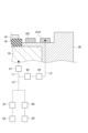


Classifications
-
- H—ELECTRICITY
- H01—ELECTRIC ELEMENTS
- H01J—ELECTRIC DISCHARGE TUBES OR DISCHARGE LAMPS
- H01J37/00—Discharge tubes with provision for introducing objects or material to be exposed to the discharge, e.g. for the purpose of examination or processing thereof
- H01J37/32—Gas-filled discharge tubes
- H01J37/32431—Constructional details of the reactor
- H01J37/32532—Electrodes
- H01J37/32541—Shape
-
- H—ELECTRICITY
- H01—ELECTRIC ELEMENTS
- H01J—ELECTRIC DISCHARGE TUBES OR DISCHARGE LAMPS
- H01J37/00—Discharge tubes with provision for introducing objects or material to be exposed to the discharge, e.g. for the purpose of examination or processing thereof
- H01J37/32—Gas-filled discharge tubes
- H01J37/32009—Arrangements for generation of plasma specially adapted for examination or treatment of objects, e.g. plasma sources
- H01J37/32082—Radio frequency generated discharge
- H01J37/32174—Circuits specially adapted for controlling the RF discharge
-
- H—ELECTRICITY
- H01—ELECTRIC ELEMENTS
- H01J—ELECTRIC DISCHARGE TUBES OR DISCHARGE LAMPS
- H01J37/00—Discharge tubes with provision for introducing objects or material to be exposed to the discharge, e.g. for the purpose of examination or processing thereof
- H01J37/32—Gas-filled discharge tubes
- H01J37/32431—Constructional details of the reactor
- H01J37/32532—Electrodes
- H01J37/32568—Relative arrangement or disposition of electrodes; moving means
-
- H—ELECTRICITY
- H01—ELECTRIC ELEMENTS
- H01J—ELECTRIC DISCHARGE TUBES OR DISCHARGE LAMPS
- H01J37/00—Discharge tubes with provision for introducing objects or material to be exposed to the discharge, e.g. for the purpose of examination or processing thereof
- H01J37/32—Gas-filled discharge tubes
- H01J37/32009—Arrangements for generation of plasma specially adapted for examination or treatment of objects, e.g. plasma sources
- H01J37/32082—Radio frequency generated discharge
- H01J37/32174—Circuits specially adapted for controlling the RF discharge
- H01J37/32183—Matching circuits
-
- H—ELECTRICITY
- H01—ELECTRIC ELEMENTS
- H01J—ELECTRIC DISCHARGE TUBES OR DISCHARGE LAMPS
- H01J37/00—Discharge tubes with provision for introducing objects or material to be exposed to the discharge, e.g. for the purpose of examination or processing thereof
- H01J37/32—Gas-filled discharge tubes
- H01J37/32431—Constructional details of the reactor
- H01J37/32623—Mechanical discharge control means
- H01J37/32642—Focus rings
-
- H—ELECTRICITY
- H01—ELECTRIC ELEMENTS
- H01J—ELECTRIC DISCHARGE TUBES OR DISCHARGE LAMPS
- H01J37/00—Discharge tubes with provision for introducing objects or material to be exposed to the discharge, e.g. for the purpose of examination or processing thereof
- H01J37/32—Gas-filled discharge tubes
- H01J37/32431—Constructional details of the reactor
- H01J37/32623—Mechanical discharge control means
- H01J37/32651—Shields, e.g. dark space shields, Faraday shields
-
- H—ELECTRICITY
- H01—ELECTRIC ELEMENTS
- H01J—ELECTRIC DISCHARGE TUBES OR DISCHARGE LAMPS
- H01J37/00—Discharge tubes with provision for introducing objects or material to be exposed to the discharge, e.g. for the purpose of examination or processing thereof
- H01J37/32—Gas-filled discharge tubes
- H01J37/32917—Plasma diagnostics
- H01J37/32935—Monitoring and controlling tubes by information coming from the object and/or discharge
-
- H—ELECTRICITY
- H10—SEMICONDUCTOR DEVICES; ELECTRIC SOLID-STATE DEVICES NOT OTHERWISE PROVIDED FOR
- H10P—GENERIC PROCESSES OR APPARATUS FOR THE MANUFACTURE OR TREATMENT OF DEVICES COVERED BY CLASS H10
- H10P72/00—Handling or holding of wafers, substrates or devices during manufacture or treatment thereof
- H10P72/70—Handling or holding of wafers, substrates or devices during manufacture or treatment thereof for supporting or gripping
- H10P72/76—Handling or holding of wafers, substrates or devices during manufacture or treatment thereof for supporting or gripping using mechanical means, e.g. clamps or pinches
- H10P72/7604—Handling or holding of wafers, substrates or devices during manufacture or treatment thereof for supporting or gripping using mechanical means, e.g. clamps or pinches the wafers being placed on a susceptor, stage or support
- H10P72/7611—Handling or holding of wafers, substrates or devices during manufacture or treatment thereof for supporting or gripping using mechanical means, e.g. clamps or pinches the wafers being placed on a susceptor, stage or support characterised by edge profile or support profile
-
- H—ELECTRICITY
- H01—ELECTRIC ELEMENTS
- H01J—ELECTRIC DISCHARGE TUBES OR DISCHARGE LAMPS
- H01J2237/00—Discharge tubes exposing object to beam, e.g. for analysis treatment, etching, imaging
- H01J2237/32—Processing objects by plasma generation
- H01J2237/33—Processing objects by plasma generation characterised by the type of processing
- H01J2237/334—Etching
-
- H—ELECTRICITY
- H01—ELECTRIC ELEMENTS
- H01J—ELECTRIC DISCHARGE TUBES OR DISCHARGE LAMPS
- H01J37/00—Discharge tubes with provision for introducing objects or material to be exposed to the discharge, e.g. for the purpose of examination or processing thereof
- H01J37/32—Gas-filled discharge tubes
- H01J37/32009—Arrangements for generation of plasma specially adapted for examination or treatment of objects, e.g. plasma sources
- H01J37/32082—Radio frequency generated discharge
- H01J37/32091—Radio frequency generated discharge the radio frequency energy being capacitively coupled to the plasma
-
- H—ELECTRICITY
- H10—SEMICONDUCTOR DEVICES; ELECTRIC SOLID-STATE DEVICES NOT OTHERWISE PROVIDED FOR
- H10P—GENERIC PROCESSES OR APPARATUS FOR THE MANUFACTURE OR TREATMENT OF DEVICES COVERED BY CLASS H10
- H10P72/00—Handling or holding of wafers, substrates or devices during manufacture or treatment thereof
- H10P72/70—Handling or holding of wafers, substrates or devices during manufacture or treatment thereof for supporting or gripping
- H10P72/72—Handling or holding of wafers, substrates or devices during manufacture or treatment thereof for supporting or gripping using electrostatic chucks
- H10P72/722—Details of electrostatic chucks
Landscapes
- Engineering & Computer Science (AREA)
- Physics & Mathematics (AREA)
- Plasma & Fusion (AREA)
- Chemical & Material Sciences (AREA)
- Analytical Chemistry (AREA)
- Power Engineering (AREA)
- Plasma Technology (AREA)
- Drying Of Semiconductors (AREA)
Description
本開示の例示的実施形態は、プラズマ処理装置に関するものである。 An exemplary embodiment of the present disclosure relates to a plasma processing apparatus.
特許文献1又は特許文献2に開示のプラズマ処理装置は、上部電極の周辺部に段差スロープを設け、周辺部におけるプラズマの密度を高めている。
The plasma processing apparatus disclosed in
上記文献によれば、上部電極の周辺部に段差スロープを設けることにより、スロープ角部近傍に電子を集中させることができるため、プラズマ生成が効率的に行われる。一方、プラズマの面内均一性を向上可能なプラズマ処理装置が求められている。 According to the above document, by providing a step slope on the periphery of the upper electrode, electrons can be concentrated near the corners of the slope, and plasma can be generated efficiently. On the other hand, there is a demand for a plasma processing apparatus that can improve the in-plane uniformity of the plasma.
一つの例示的実施形態において、プラズマ処理装置が提供される。プラズマ処理装置は、チャンバ、第1の下部電極、第2の下部電極、第1の上部電極、第2の上部電極、及び第1の電源を有している。第1の下部電極は、チャンバの内部に設けられ、基板を載置する基板載置領域を有する。第2の下部電極は、基板載置領域の外側の領域に配置されている。第1の上部電極は、基板載置領域と対向して配置されている。第2の上部電極は、第1の上部電極の外側の領域に配置され、第2の下部電極と対向して配置されている。第1の電源は、第1の下部電極に周期性を有する信号を供給する。第2の下部電極及び第2の上部電極の少なくとも一方は凹部を有する。凹部の表面に対する法線上に第2の下部電極又は第2の上部電極が位置する。 In one exemplary embodiment, a plasma processing apparatus is provided. The plasma processing apparatus includes a chamber, a first lower electrode, a second lower electrode, a first upper electrode, a second upper electrode, and a first power supply. The first lower electrode is provided inside the chamber and has a substrate placement area on which a substrate is placed. The second lower electrode is disposed in an area outside the substrate placement area. The first upper electrode is disposed opposite the substrate placement area. The second upper electrode is disposed in an area outside the first upper electrode and opposite the second lower electrode. The first power supply supplies a periodic signal to the first lower electrode. At least one of the second lower electrode and the second upper electrode has a recess. The second lower electrode or the second upper electrode is located on a normal line to the surface of the recess.
プラズマ処理装置によれば、プラズマの面内均一性を向上させることができる。 The plasma processing apparatus can improve the in-plane uniformity of the plasma.
以下、種々の例示的実施形態について説明する。 Various exemplary embodiments are described below.
一つの例示的実施形態において、プラズマ処理装置が提供される。プラズマ処理装置は、チャンバ、第1の下部電極、第2の下部電極、第1の上部電極、第2の上部電極、及び第1の電源を有している。第1の下部電極は、チャンバの内部に設けられ、基板を載置する基板載置領域を有する。第2の下部電極は、基板載置領域の外側の領域(以下、基板周辺領域という)に配置されている。第1の上部電極は、基板載置領域と対向して配置されている。第2の上部電極は、第1の上部電極の外側の領域に配置され、第2の下部電極と対向して配置されている。第1の電源は、第1の下部電極に周期性を有する信号を供給する。第2の下部電極及び第2の上部電極の少なくとも一方は凹部を有する。凹部の表面に対する法線上に第2の下部電極又は第2の上部電極が位置する。 In one exemplary embodiment, a plasma processing apparatus is provided. The plasma processing apparatus includes a chamber, a first lower electrode, a second lower electrode, a first upper electrode, a second upper electrode, and a first power supply. The first lower electrode is provided inside the chamber and has a substrate placement area on which a substrate is placed. The second lower electrode is disposed in an area outside the substrate placement area (hereinafter referred to as a substrate peripheral area). The first upper electrode is disposed opposite the substrate placement area. The second upper electrode is disposed in an area outside the first upper electrode and opposite the second lower electrode. The first power supply supplies a periodic signal to the first lower electrode. At least one of the second lower electrode and the second upper electrode has a recess. The second lower electrode or the second upper electrode is located on a normal line to the surface of the recess.
第2の下部電極及び第2の上部電極の少なくとも一方は凹部を有する。一方の凹部の表面近傍から他方に向けて加速される電子は集束するため、基板周辺領域におけるプラズマ密度が増加し、基板載置領域の中心部におけるプラズマ密度が高くなること抑制することができる。したがって、プラズマの面内均一性を高くすることができる。 At least one of the second lower electrode and the second upper electrode has a recess. Electrons accelerated from near the surface of one recess toward the other are focused, so that the plasma density in the peripheral region of the substrate increases, and it is possible to prevent the plasma density in the center of the substrate placement region from becoming high. Therefore, it is possible to improve the in-plane uniformity of the plasma.
一つの例示的実施形態において、第2の下部電極及び第2の上部電極の双方が凹部を有してもよい。第2の下部電極の凹部の表面に対する法線上に第2の上部電極の凹部が位置し、且つ、第2の上部電極の凹部の表面に対する法線上に前記第2の下部電極の凹部が位置してもよい。第2の下部電極及び第2の上部電極において、一方の凹部の表面近傍から、他方の凹部に向けて加速される電子は集束される。逆に、他方の凹部の表面近傍から、一方の凹部に向けて加速される電子も集束される。したがって、基板周辺領域におけるプラズマ密度が増加する。これにより、基板載置領域の中心部におけるプラズマ密度の増加を抑制することができる。したがって、プラズマの面内均一性を高くすることができる。 In one exemplary embodiment, both the second lower electrode and the second upper electrode may have a recess. The recess of the second upper electrode may be located on a normal line to the surface of the recess of the second lower electrode, and the recess of the second lower electrode may be located on a normal line to the surface of the recess of the second upper electrode. In the second lower electrode and the second upper electrode, electrons accelerated from the vicinity of the surface of one recess toward the other recess are focused. Conversely, electrons accelerated from the vicinity of the surface of the other recess toward one recess are also focused. Therefore, the plasma density in the substrate peripheral region increases. This makes it possible to suppress the increase in plasma density in the center of the substrate placement region. Therefore, the in-plane uniformity of the plasma can be increased.
一つの例示的実施形態において、プラズマ処理装置は、第2の上部電極に直流電圧を供給する第2の電源を更に有してもよい。第2の上部電極に直流電圧が供給されると、第2の上部電極に向かう電子に力を与えることができ、第2の上部電極の近傍におけるプラズマ密度を制御することができる。この電子に斥力を与えると、第2の上部電極から、電子は離れる方向に移動し、基板周辺領域におけるプラズマ密度が増加する。これにより、基板載置領域の中心部におけるプラズマ密度と、基板周辺領域におけるプラズマ密度の比率を調整することができる。したがって、プラズマの面内均一性を高くすることができる。 In one exemplary embodiment, the plasma processing apparatus may further include a second power supply that supplies a DC voltage to the second upper electrode. When a DC voltage is supplied to the second upper electrode, a force can be applied to the electrons moving toward the second upper electrode, and the plasma density in the vicinity of the second upper electrode can be controlled. When a repulsive force is applied to the electrons, the electrons move away from the second upper electrode, and the plasma density in the peripheral region of the substrate increases. This makes it possible to adjust the ratio of the plasma density in the center of the substrate placement region to the plasma density in the peripheral region of the substrate. Therefore, the in-plane uniformity of the plasma can be increased.
一つの例示的実施形態において、プラズマ処理装置は、第2の上部電極に周期性を有する信号を供給する第3の電源を更に有してもよい。第2の上部電極に、周期性を有する信号が与えられると、第2の上部電極の近傍において発生するプラズマの密度を向上させることができる。したがって、上述のように、プラズマの面内均一性を高くすることができる。 In one exemplary embodiment, the plasma processing apparatus may further include a third power supply that supplies a periodic signal to the second upper electrode. When a periodic signal is applied to the second upper electrode, the density of the plasma generated in the vicinity of the second upper electrode can be improved. Therefore, as described above, the in-plane uniformity of the plasma can be increased.
一つの例示的実施形態において、プラズマ処理装置は、第1の給電ラインと、第2の給電ラインとを有してもよい。第1の給電ラインは、第3の電源から出力された周期性を有する信号を第1の上部電極に供給する。第2の給電ラインは、第3の電源から出力された周期性を有する信号を第2の上部電極に供給する。第1の給電ライン又は第2の給電ラインに可変インピーダンス回路を有してもよい。 In one exemplary embodiment, the plasma processing apparatus may have a first power supply line and a second power supply line. The first power supply line supplies a periodic signal output from a third power supply to the first upper electrode. The second power supply line supplies a periodic signal output from the third power supply to the second upper electrode. The first power supply line or the second power supply line may have a variable impedance circuit.
可変インピーダンス回路におけるインピーダンスを調整することにより、対象となる上部電極への電力供給量を調整することができる。したがって。第1の上部電極と第2の上部電極に供給される電力の比率を調整することができる。プラズマ密度は、対象となる電極への電力供給量に依存する。したがって、電力供給量の比率を調整することで、プラズマの面内均一性を高くすることができる。 By adjusting the impedance in the variable impedance circuit, the amount of power supplied to the target upper electrode can be adjusted. Therefore, the ratio of the power supplied to the first upper electrode and the second upper electrode can be adjusted. Plasma density depends on the amount of power supplied to the target electrode. Therefore, by adjusting the ratio of the power supplies, the in-plane uniformity of the plasma can be improved.
一つの例示的実施形態において、プラズマ処理装置は、第2の下部電極に直流電圧を供給する第4の電源を更に備えることとしてもよい。第2の下部電極に直流電圧が供給されると、第2の下部電極に向かう電子に力を与えることができ、第2の下部電極の近傍におけるプラズマ密度を制御することができる。この電子に斥力を与えると、第2の下部電極から、電子は離れる方向に移動し、基板周辺領域におけるプラズマ密度が増加する。したがって、上述のように、プラズマの面内均一性を高くすることができる。 In one exemplary embodiment, the plasma processing apparatus may further include a fourth power supply that supplies a DC voltage to the second lower electrode. When a DC voltage is supplied to the second lower electrode, a force can be applied to the electrons moving toward the second lower electrode, and the plasma density in the vicinity of the second lower electrode can be controlled. When a repulsive force is applied to the electrons, the electrons move away from the second lower electrode, and the plasma density in the peripheral region of the substrate increases. Therefore, as described above, the in-plane uniformity of the plasma can be increased.
一つの例示的実施形態において、プラズマ処理装置は、第3の給電ラインと、第4の給電ラインとを有してもよい。第3の給電ラインは、第1の電源から出力された周期性を有する信号を第1の下部電極に供給する。第4の給電ラインは、第1の電源から出力された周期性を有する信号を第2の下部電極に供給する。プラズマ処理装置は、第3の給電ライン又は第4の給電ラインに可変インピーダンス回路を有することとしてもよい。 In one exemplary embodiment, the plasma processing apparatus may have a third power supply line and a fourth power supply line. The third power supply line supplies the periodic signal output from the first power supply to the first lower electrode. The fourth power supply line supplies the periodic signal output from the first power supply to the second lower electrode. The plasma processing apparatus may have a variable impedance circuit in the third power supply line or the fourth power supply line.
可変インピーダンス回路におけるインピーダンスを調整することにより、対象となる下部電極への電力供給量を調整することができる。したがって、第1の下部電極と第2の下部電極に供給される電力の比率を調整することができる。プラズマ密度は、対象となる電極への電力供給量に依存する。したがって、電力供給量の比率を調整することで、プラズマの面内均一性を高くすることができる。 By adjusting the impedance in the variable impedance circuit, the amount of power supplied to the target lower electrode can be adjusted. Thus, the ratio of power supplied to the first lower electrode and the second lower electrode can be adjusted. Plasma density depends on the amount of power supplied to the target electrodes. Therefore, by adjusting the ratio of the power supplies, the in-plane uniformity of the plasma can be improved.
一つの例示的実施形態において、プラズマ処理装置は、第2の下部電極に周期性を有する信号を供給する第5の電源を更に備えてもよい。第2の下部電極に、周期性を有する信号が与えられると、第2の下部電極の近傍において発生するプラズマの密度を向上させることができる。したがって、上述のように、プラズマの面内均一性を高くすることができる。 In one exemplary embodiment, the plasma processing apparatus may further include a fifth power supply that supplies a periodic signal to the second lower electrode. When a periodic signal is applied to the second lower electrode, the density of the plasma generated in the vicinity of the second lower electrode can be improved. Therefore, as described above, the in-plane uniformity of the plasma can be improved.
一つの例示的実施形態において、プラズマ処理装置は、第2の下部電極又は第2の上部電極に発生する自己バイアス電圧又は電圧波形を計測するセンサーを更に有してもよい。プラズマ処理装置は、センサーより計測された計測値に応じて可変インピーダンス回路のインピーダンスを制御する制御部を有してもよい。 In one exemplary embodiment, the plasma processing apparatus may further include a sensor that measures the self-bias voltage or voltage waveform generated in the second lower electrode or the second upper electrode. The plasma processing apparatus may include a control unit that controls the impedance of the variable impedance circuit according to the measurement value measured by the sensor.
可変インピーダンス回路のインピーダンスは、基板載置領域上の空間(第1の下部電極と第1の上部電極との間の空間)と、基板周辺領域上の空間(第2の下部電極と第2の上部電極との間の空間)内に発生するプラズマ密度を制御する。センサーにより計測された計測値は、基板周辺領域内におけるプラズマ密度に相関する。したがって、制御部が、計測値に対応するプラズマ密度に応じて、可変インピーダンス回路のインピーダンスを調整することで、可変インピーダンス回路に接続された電極への電力供給量を調整することができる。プラズマ密度は、対象となる電極への電力供給量に依存する。したがって、センサーによる計測値に基づき、電力供給量の比率を調整することで、プラズマの面内均一性を高くすることができる。 The impedance of the variable impedance circuit controls the plasma density generated in the space above the substrate placement area (the space between the first lower electrode and the first upper electrode) and the space above the substrate peripheral area (the space between the second lower electrode and the second upper electrode). The measurement value measured by the sensor correlates with the plasma density in the substrate peripheral area. Therefore, the control unit can adjust the amount of power supplied to the electrode connected to the variable impedance circuit by adjusting the impedance of the variable impedance circuit according to the plasma density corresponding to the measurement value. Plasma density depends on the amount of power supplied to the target electrode. Therefore, the in-plane uniformity of the plasma can be improved by adjusting the ratio of the power supply based on the measurement value by the sensor.
一つの例示的実施形態において、プラズマ処理装置は、第2の下部電極に発生する自己バイアス電圧又は電圧波形を計測するセンサーを更に有してもよい。プラズマ処理装置は、センサーより計測された計測値に応じて第2の電源の出力を制御する制御部を有してもよい。 In one exemplary embodiment, the plasma processing apparatus may further include a sensor that measures the self-bias voltage or voltage waveform generated in the second lower electrode. The plasma processing apparatus may also include a control unit that controls the output of the second power supply in response to the measurement value measured by the sensor.
センサーにより計測された計測値は、第2の下部電極によって反射される電子量、すなわち、基板周辺領域におけるプラズマ密度に相関する。また、第2の電源の出力を調整することにより、プラズマ密度を調整することができる。したがって、制御部が、計測値に対応するプラズマ密度に応じて、第2の電源の出力を調整することで、基板周辺領域におけるプラズマ密度を制御することができる。したがって、プラズマの面内均一性を高くすることができる。 The measurement value obtained by the sensor correlates with the amount of electrons reflected by the second lower electrode, i.e., the plasma density in the peripheral region of the substrate. In addition, the plasma density can be adjusted by adjusting the output of the second power supply. Therefore, the control unit can control the plasma density in the peripheral region of the substrate by adjusting the output of the second power supply according to the plasma density corresponding to the measurement value. Therefore, the in-plane uniformity of the plasma can be improved.
一つの例示的実施形態において、プラズマ処理装置は、第2の下部電極に発生する自己バイアス電圧又は電圧波形を計測するセンサーを更に有してもよい。プラズマ処理装置は、センサーより計測された計測値に応じて第5の電源の出力を制御する制御部を有してもよい。 In one exemplary embodiment, the plasma processing apparatus may further include a sensor that measures the self-bias voltage or voltage waveform generated in the second lower electrode. The plasma processing apparatus may include a control unit that controls the output of the fifth power supply according to the measurement value measured by the sensor.
センサーにより計測された計測値は、第2の下部電極によって反射される電子量、すなわち、基板周辺領域におけるプラズマ密度に相関する。制御部が、計測値に対応するプラズマ密度に応じて、第5の電源の出力を調整すると、基板周辺領域におけるプラズマ密度を制御することができる。したがって、上述のように、プラズマの面内均一性を高くすることができる。 The measurement value obtained by the sensor correlates with the amount of electrons reflected by the second lower electrode, i.e., the plasma density in the peripheral region of the substrate. When the control unit adjusts the output of the fifth power supply according to the plasma density corresponding to the measurement value, the plasma density in the peripheral region of the substrate can be controlled. Therefore, as described above, the in-plane uniformity of the plasma can be improved.
一つの例示的実施形態において、制御部は、第2の上部電極に、第2の下部電極に発生する自己バイアス電圧の大きさ以上の大きさの負の直流電圧が発生するように第2の電源の出力を制御してもよい。 In one exemplary embodiment, the control unit may control the output of the second power supply so that a negative DC voltage is generated on the second upper electrode that is equal to or greater than the self-bias voltage generated on the second lower electrode.
第2の上部電極に、負の直流電圧が与えられると、第2の上部電極に向かう電子に斥力が与えられ、反射される。反射された電子は、プラズマ領域へと進行し、プラズマ発生に寄与するので、基板周辺領域におけるプラズマ密度が増加する。したがって、上述のように、プラズマの面内均一性を高くすることができる。 When a negative DC voltage is applied to the second upper electrode, a repulsive force is applied to the electrons heading toward the second upper electrode, causing them to be reflected. The reflected electrons proceed to the plasma region and contribute to plasma generation, increasing the plasma density in the peripheral region of the substrate. Therefore, as described above, the in-plane uniformity of the plasma can be increased.
一つの例示的実施形態において、第2の下部電極及び第2の上部電極は、電気的に接地されていてもよい。第2の下部電極と第2の上部電極との間に、プラスの電位のプラズマのシースが形成されている場合、これらの電極近傍の電子は、シースの方に進行する。シース方向に移動した電子は、プラズマ発生に寄与するので、基板周辺領域におけるプラズマ密度が増加する。したがって、上述のように、プラズマの面内均一性を高くすることができる。 In one exemplary embodiment, the second lower electrode and the second upper electrode may be electrically grounded. When a plasma sheath of positive potential is formed between the second lower electrode and the second upper electrode, electrons near these electrodes travel toward the sheath. The electrons that move toward the sheath contribute to plasma generation, increasing the plasma density in the peripheral region of the substrate. Therefore, as described above, the in-plane uniformity of the plasma can be increased.
一つの例示的実施形態において、第2の上部電極と第2の下部電極との間の間隔が、第1の上部電極と第1の下部電極との間の間隔よりも狭くてもよい。これにより、基板周辺領域(第2の上部電極と第2の下部電極との間の領域)における電界を強くし、この領域におけるプラズマ密度を高めることができる。したがって、上述のように、プラズマの面内均一性を高くすることができる。 In one exemplary embodiment, the distance between the second upper electrode and the second lower electrode may be narrower than the distance between the first upper electrode and the first lower electrode. This strengthens the electric field in the region around the substrate (the region between the second upper electrode and the second lower electrode), and increases the plasma density in this region. Therefore, as described above, the in-plane uniformity of the plasma can be increased.
一つの例示的実施形態において、プラズマ処理装置は、基板が載置される基板載置領域と第2の下部電極との間に、導電性のエッジリングを有してもよい。エッジリングは、基板載置領域の周辺部における電界を調整することができる。したがって、プラズマ処理の均一性を向上させることができる。 In one exemplary embodiment, the plasma processing apparatus may have a conductive edge ring between the substrate placement area on which the substrate is placed and the second lower electrode. The edge ring can adjust the electric field at the periphery of the substrate placement area. Therefore, the uniformity of the plasma processing can be improved.
一つの例示的実施形態において、第2の上部電極及び第2の下部電極は、凹部の底面に対する法線が基板載置領域に対する法線に対して傾斜するように配置されてもよい。第2の上部電極と第2の下部電極との間の距離、及び/又は上記傾斜角度を変更することで、基板周辺領域における、プラズマの強度や形状を変更することができる。プラズマ密度の面内分布の設計自由度が向上するので、プラズマの面内均一性を高くすることができる。 In one exemplary embodiment, the second upper electrode and the second lower electrode may be arranged such that the normal to the bottom surface of the recess is inclined with respect to the normal to the substrate placement region. By changing the distance between the second upper electrode and the second lower electrode and/or the inclination angle, the intensity and shape of the plasma in the region surrounding the substrate can be changed. This improves the design freedom of the in-plane distribution of the plasma density, thereby improving the in-plane uniformity of the plasma.
一つの例示的実施形態において、第2の上部電極が、チャンバの内壁又はチャンバの内壁に沿って設けられたデポシールドにより構成されてもよい。この場合、第2の上部電極は、チャンバの内壁又はデポシールドを兼用しているので、上述の作用効果を奏しつつ、部品点数を少なくすることができる。 In one exemplary embodiment, the second upper electrode may be configured as an inner wall of the chamber or a deposit shield provided along the inner wall of the chamber. In this case, the second upper electrode also serves as the inner wall of the chamber or the deposit shield, so that the number of parts can be reduced while still achieving the above-mentioned effects.
以下、図面を参照して種々の例示的実施形態について詳細に説明する。なお、各図面において同一又は相当の部分に対しては同一の符号を附することとし、重複する説明は省略する。 Various exemplary embodiments will be described in detail below with reference to the drawings. Note that the same or equivalent parts in each drawing will be given the same reference numerals, and duplicate explanations will be omitted.
図1は、例示的実施形態に係るプラズマ処理装置1の基本構造を示す図である。本実施形態におけるプラズマ処理装置1は、例えば容量結合型平行平板プラズマエッチング装置である。プラズマ処理装置1は、例えば表面が陽極酸化処理されたアルミニウムによって形成された略円筒状のチャンバ10を有する。チャンバ10は保安接地されている。
Figure 1 is a diagram showing the basic structure of a
チャンバ10の底部には、セラミックス等によって形成された絶縁板を介して、円柱状の支持台14が配置されている。支持台14の上に例えばアルミニウム等で形成された載置台16が設けられている。載置台16は下部電極(第1の下部電極)として機能する。
A cylindrical support table 14 is placed on the bottom of the
載置台16は、基板が載置される基板載置領域を有する。載置台16の上面には、基板の一例である半導体ウエハWを静電力で吸着保持する静電チャック18が設けられている。静電チャック18は、導電膜で形成された電極20を一対の絶縁層又は絶縁シートで挟んだ構造を有する。電極20には直流電源SGが電気的に接続されている。半導体ウエハWは、静電チャック18の上面に載置され、直流電源SGから供給された直流電圧により生じた静電力により、静電チャック18に吸着保持される。半導体ウエハWが載置される静電チャック18の上面は、載置台16の基板載置領域の一例である。
The mounting table 16 has a substrate mounting area on which a substrate is placed. An
載置台16の上面には、エッジリングERが設けられる。エッジリングERは、基板載置領域を取り囲むように設けられる。エッジリングERは、環状の形状を有し、静電チャック18の鉛直方向の中心軸とエッジリングERの鉛直方向の中心軸とが一致するように配置されている。エッジリングERは、シリコン等の導電性材料で形成されている。エッジリングERは、静電チャック18の上に配置してもよい。上方から見た場合、エッジリングERは、基板載置領域と補助電極AUXとの間に設けられている。エッジリングERは、基板載置領域の周辺部において、活性種が、鉛直方向(基板表面に垂直な方向)に沿って進行するように電界を調整することができる。エッジリングERにより、エッチング等のプラズマ処理の均一性が向上する。載置台16及び支持台14の側面には、例えば石英で形成された円筒状の内壁部材を含む絶縁部材26が設けられている。絶縁部材26は複数の部品から構成することができ、内部に導電性の配線なども配置することができる。
An edge ring ER is provided on the upper surface of the mounting table 16. The edge ring ER is provided so as to surround the substrate mounting area. The edge ring ER has an annular shape and is arranged so that the vertical central axis of the
補助電極AUXは、エッジリングERの外周側に設けられた環状の部材であり、静電チャック18の鉛直方向の中心軸と補助電極AUXの鉛直方向の中心軸とが一致するように配置されている。すなわち、補助電極AUXは、エッジリングERと同心円状に配置されており、基板載置領域の外側の領域(基板周辺領域)に配置されている。補助電極AUXは、シリコン等の導電性材料で形成されており、絶縁部材26上に載置されている。
The auxiliary electrode AUX is an annular member provided on the outer periphery of the edge ring ER, and is arranged so that the vertical central axis of the
載置台16の内部には、例えば環状の冷媒室が形成されている。この冷媒室には、外部に設けられたチラーユニットから、配管を介して、冷却水等の所定温度の冷媒が循環供給される。冷媒室内を循環する冷媒によって、載置台16及び静電チャック18の温度が制御され、静電チャック18上の半導体ウエハWが所定温度に制御される。
Inside the mounting table 16, for example, a ring-shaped coolant chamber is formed. A coolant at a predetermined temperature, such as cooling water, is circulated and supplied to this coolant chamber from an external chiller unit via piping. The coolant circulating inside the coolant chamber controls the temperatures of the mounting table 16 and the
また、図示しない伝熱ガス供給機構からのHeガス等の伝熱ガスが、載置台16の内部の配管を介して、静電チャック18の上面と半導体ウエハWの裏面との間に供給される。
In addition, a heat transfer gas such as He gas from a heat transfer gas supply mechanism (not shown) is supplied between the upper surface of the
下部電極として機能する載置台16の上方には、載置台16と対向するように上部電極34が設けられている。上部電極34と、載置台16との間の空間がプラズマ生成空間となり、この空間内においてプラズマPLが生成される。
An
上部電極34は、絶縁性遮蔽部材42を介して、チャンバ10の上部に支持されている。絶縁性遮蔽部材42は、内面に支持用の段差が設けられた円筒形の絶縁部材であってもよい。上部電極34は、第1の電極板36(第1の上部電極)と、第2の電極板35(第2の上部電極)と、電極支持体38とを有する。第1の電極板36は、載置台16との対向面を構成し、多数の吐出孔37を有する。第1の電極板36及び第2の電極板35は、ジュール熱の少ない低抵抗の導電体又は半導体が好ましく、例えばシリコンやSiCで形成されることが好ましい。第2の電極板35は、環状の形状を有し、第1の電極板36を囲むように第1の電極板36の周囲に同心円状に設けられている。第1の電極板36は、エッジリングER及び静電チャック18の上方の位置に設けられる。第2の電極板35は、補助電極AUXの上方の位置に設けられる。第2の電極板35は、絶縁性部材39により第1の電極板36と絶縁されている。なお、上部電極34に高周波電力を印加する場合は、絶縁性部材39を高周波電流が流れるように薄く形成してもよい。図示される第1の電極板36及び第2の電極板35は、一例であり、種々の変形が可能である。
The
電極支持体38は、第1の電極板36及び第2の電極板35を着脱自在に支持する。また、電極支持体38は、例えば表面が陽極酸化処理されたアルミニウム等の導電性材料によって形成された水冷構造を有する。電極支持体38の内部には、ガス拡散室40が設けられている。ガス拡散室40からは吐出孔37に連通する多数のガス流通孔41が下方に延びている。
The
電極支持体38にはガス拡散室40へ処理ガスを導くガス導入口62が形成されており、ガス導入口62にはガス供給管64が接続されている。ガス供給管64にはバルブ70及びマスフローコントローラ(MFC)68を介して処理ガス供給源66が接続されている。半導体ウエハWに対してエッチングの処理が行われる場合、処理ガス供給源66からは、エッチングのための処理ガスが、ガス供給管64を介してガス拡散室40に供給される。ガス拡散室40内に供給された処理ガスは、ガス拡散室40内で拡散し、それぞれのガス流通孔41及び吐出孔37を介してプラズマ処理空間内にシャワー状に吐出される。すなわち、上部電極34は、プラズマ処理空間内に処理ガスを供給するためのシャワーヘッドとしても機能する。
The
第2の電極板35には、ローパスフィルタ(LPF)46及びスイッチ47を介して、電源SBが電気的に接続されている。本例の電源SBは、可変直流電源である。電源SBは、制御部95から指示された大きさ(絶対値)の負の直流電圧を出力する。スイッチ47は、電源SBから第2の電極板35への負の直流電圧の供給及び遮断を制御する。
The power supply SB is electrically connected to the
なお、制御部95は、コンピュータの中央処理装置(CPU)から構成することができ、記憶部97に格納された処理工程を実行することができる。ユーザインターフェイス96がキーボードやボタン等の入力装置である場合には、入力装置から制御部95に、命令を入力することができる。ユーザインターフェイス96がディスプレイ等の出力装置である場合には、制御部95からの処理結果を表示することができる。
The
上部電極34の高さ位置よりも上方のチャンバ10の側壁には、円筒状の接地導体10aが設けられている。接地導体10aは、その上部に天壁を有している。
A
下部電極として機能する載置台16には、第1の整合器87を介して、電源SAが電気的に接続されている。本例の電源SAは、周期性を有する信号を発生する高周波電源である。本明細書において、周期性を有する信号とは、周期的に変化する電圧波形および電流波形を有する電気信号であり、高周波電源またはパルス電源により出力される電気信号をいう。また、周期的な任意信号を増幅器で増幅させた電気信号も含まれる。また、載置台16には、第2の整合器88を介して、電源SFが電気的に接続されている。本例の電源SFも、周期性を有する信号を発生する高周波電源であるが、電源SAとは電力の周波数が異なる。電源SAは、プラズマ発生用の電源であり、13MHz以上の周波数、例えば40MHzの第1の高周波電力を出力する。電源SFは、イオン引き込み用の電源であり、電源SAの高周波電力より低い周波数であって、27MHz以下の周波数、例えば2MHzの第2の高周波電力を出力する。電源SFの代わりに、周期性を有する信号を発生する電源として、パルス状の負極性の電圧を周期的に出力するパルス電源を用いても良い。パルス電源としては、負極性の直流電圧を周期的に出力する直流パルス電源でもよいし、負極性の電圧を瞬時的かつ周期的に出力するインパルス電源であってもよい。
The power source SA is electrically connected to the mounting table 16, which functions as the lower electrode, via a
第1の整合器87は、チャンバ10内にプラズマが生成されている時に、電源SAのインピーダンスと負荷インピーダンスとが見かけ上一致するように、電源SAのインピーダンスと負荷インピーダンスとを整合させる。同様に、第2の整合器88は、チャンバ10内にプラズマが生成されている時に、電源SFのインピーダンスと負荷インピーダンスとが見かけ上一致するように、電源SFのインピーダンスと負荷インピーダンスとを整合させる。
The
チャンバ10の底部には排気口が設けられており、排気管を介して排気装置84が接続されている。排気装置84は、ターボ分子ポンプ等の真空ポンプを有しており、チャンバ10内を所望の真空度まで減圧することができる。また、チャンバ10の側壁には半導体ウエハWを搬入及び搬出するための開口85が設けられており、開口85はゲートバルブ86により開閉可能となっている。
An exhaust port is provided at the bottom of the
チャンバ10の内壁には、チャンバ10の内壁にエッチング副生物(デポ)が付着することを防止するためのデポシールドが、チャンバ10の内壁に沿って、設けられている。また、デポシールドは、絶縁部材26の外周にも設けられている。チャンバ10の底部のチャンバ壁側のデポシールドと絶縁部材26側のデポシールドとの間には図示しない排気プレートが設けられている。デポシールド及び排気プレートとしては、例えばアルミニウム材にY2O3等のセラミックスが被覆されたものを好適に用いることができる。デポシールドは、接地電位(グランド)に電気的に接続することができ、チャンバ10内の異常放電を防止することができる。
A deposit shield for preventing etching by-products (deposits) from adhering to the inner wall of the
プラズマ処理装置1の各構成部は、制御部95によって制御される。制御部95には、工程管理者がプラズマ処理装置1を管理するためにコマンドの入力操作等を行うキーボードや、プラズマ処理装置1の稼働状況を可視化して表示するディスプレイ等からなるユーザインターフェイス96が接続されている。
Each component of the
プログラムには、プラズマ処理装置1で実行される各種処理を制御部95の制御にて実現するための制御プログラム等や、処理条件に応じてプラズマ処理装置1の各構成部に処理を実行させるものがある。これらのプログラムや処理条件を示すレシピは記憶部97に格納され、記憶部97は制御部95に接続されている。記憶部97は、例えばハードディスクや半導体メモリである。また、記憶部97は、コンピュータにより読み取り可能な可搬性の記憶媒体であってもよい。この場合、制御部95は、該記憶媒体からデータを読み取る装置を経由して、該記憶媒体に記憶された制御プログラム等を取得する。記憶媒体は、例えば、CD-ROMやDVD等である。
The programs include control programs for implementing various processes executed by the
制御部95は、ユーザインターフェイス96を介したユーザからの指示等に応じて、任意のレシピを記憶部97から読み出して実行することにより、プラズマ処理装置1の各部を制御し、半導体ウエハWに対して所定のプラズマ処理を施す。なお、本実施形態におけるプラズマ処理装置1は、制御部95、ユーザインターフェイス96、及び記憶部97を含む。
The
このように構成されたプラズマ処理装置1において、半導体ウエハWに対してエッチング処理が行われる場合、まず、ゲートバルブ86が開状態に制御され、開口85を介してエッチング対象の半導体ウエハWがチャンバ10内に搬入される。次に、半導体ウエハWは、静電チャック18上に載置される。そして、直流電源SGから所定の直流電圧が静電チャック18に印加され、半導体ウエハWが静電チャック18の上面に吸着保持される。
When etching is performed on a semiconductor wafer W in the
そして、処理ガス供給源66からエッチング等のための処理ガスが、所定の流量でガス拡散室40へ供給され、ガス流通孔41及び吐出孔37を介して処理ガスがチャンバ10内に供給される。また、排気装置84によりチャンバ10内が排気され、チャンバ10内の圧力が所定の圧力に制御される。チャンバ10内に処理ガスが供給された状態で、電源SAからプラズマ生成用の高周波電力が載置台16に印加されるとともに、電源SFからイオン引き込み用の高周波電力が載置台16に印加される。また、電源SBから所定の大きさの負の直流電圧(電位)が第2の電極板35に印加される。
Then, a processing gas for etching or the like is supplied from the processing
上部電極34の吐出孔37から吐出された処理ガスは、載置台16に印加された高周波電力により、上部電極34と載置台16との間でプラズマ化する。このプラズマで生成されるラジカルやイオンによって半導体ウエハWがエッチングされる。上記の処理は、制御部95からの指示により実行される。
The process gas discharged from the discharge holes 37 of the
次に、補助電極の電位について説明する。 Next, we will explain the potential of the auxiliary electrode.
図2は、図1に示したプラズマ処理装置の主要部の基本構造の縦断面構成を示す図である。 Figure 2 shows a vertical cross-sectional view of the basic structure of the main parts of the plasma processing device shown in Figure 1.
エッジリングER及び補助電極AUXは、石英リング等の複数の部品からなる絶縁部材26上に載置されている。絶縁部材26のエッジリングERが載置されている部分は薄く形成されており、載置台16を介して、電源SA及び電源SFからの高周波電流が、エッジリングERに流れるようになっている。補助電極AUXは、エッジリングERに寄生容量Cを介して結合している。また、絶縁部材26の補助電極AUXが載置されている部分が薄く形成されている場合、載置台16を介して、電源SA及び電源SFからの高周波電流が、補助電極AUXに流れる。このため、補助電極AUXは周期的に変動する電位を有する。また、補助電極AUXには負の直流電圧である自己バイアス電圧が発生するため、補助電極AUXの電位は自己バイアス電圧Vdcを基準として周期的に変動する。
The edge ring ER and the auxiliary electrode AUX are placed on an insulating
補助電極AUXと対向する第2の電極板35には、電源SBにより、-V2の直流電圧が印加される。負の電荷(‐)を有する電子は、補助電極AUXとプラズマとの間の電界及びプラズマと第2の電極板35との間の電界に応じて移動する。
A DC voltage of -V2 is applied from the power supply SB to the
図3は、鉛直方向の位置Zと電位V(a.u.)との関係を示すグラフであり、補助電極AUXと第2の電極板35との間の電位分布を模式的に示している。なお、プラズマ処理装置の鉛直上方をZ軸正方向とし、各電位は接地電位(V=0)を基準とする電圧を示している。また、第2の電極板35に印加される負の電圧-V2の大きさ(絶対値)は、補助電極AUXに生じる負の電圧である自己バイアス電圧Vdcの大きさ(絶対値)と等しく設定することもできる。
Figure 3 is a graph showing the relationship between vertical position Z and potential V (a.u.), and shows a schematic of the potential distribution between the auxiliary electrode AUX and the
補助電極AUXの電位は、自己バイアス電圧Vdcを基準として、最大値Vmaxから最小値Vminの間で周期的に変動している。補助電極AUXの電位が、自己バイアス電圧Vdcの場合には、実線で示される電位分布となる。補助電極AUXの電位が、最大値Vmax又は最小値Vminをとる場合は、点線で示される電位分布となる。補助電極AUXの電位の変動に応じて、補助電極AUXとプラズマとの間のシース厚さは変動する。 The potential of the auxiliary electrode AUX periodically varies between a maximum value Vmax and a minimum value Vmin, with the self-bias voltage Vdc as the reference. When the potential of the auxiliary electrode AUX is the self-bias voltage Vdc, the potential distribution is as shown by the solid line. When the potential of the auxiliary electrode AUX is the maximum value Vmax or the minimum value Vmin, the potential distribution is as shown by the dotted line. The sheath thickness between the auxiliary electrode AUX and the plasma varies according to the variation in the potential of the auxiliary electrode AUX.
シースが薄いときに補助電極AUX近傍のプラズマ中に存在した電子は、シースが厚くなると補助電極AUXの表面に垂直にかかる高電界により、力を受ける。この力を受けた電子は、補助電極AUXと対向する第2の電極板35に向かって(プラズマに向かって)加速される。また、補助電極AUXにイオンが衝突することにより生じた二次電子も同様に、補助電極AUXとプラズマとの間のシース電界により、力を受ける。この力を受けた電子は、第2の電極板35に向かって(プラズマに向かって)加速される。これら加速された電子の一部は、プラズマ中の粒子と衝突し、プラズマ密度の向上に寄与する。一方、プラズマ中の粒子と衝突しなかった残りの加速電子は、第2の電極板35に向かって進行する。
When the sheath is thin, electrons present in the plasma near the auxiliary electrode AUX are subjected to a force by the high electric field perpendicular to the surface of the auxiliary electrode AUX when the sheath becomes thicker. The electrons subjected to this force are accelerated toward the
第2の電極板35に向かって進行した加速電子は、第2の電極板35とプラズマとの間のシース電界により斥力を受ける。シース電界の強さはプラズマ電位と壁電位との差に比例する。したがって、プラズマ電位と第2の電極板35の電位(壁電位)との差が、プラズマ電位と補助電極AUXの電位(壁電位)との差よりも小さければ(進入条件)、加速電子は第2の電極板35に進入することになる。
The accelerated electrons traveling toward the
また、プラズマ電位と第2の電極板35の電位(壁電位)との差が、プラズマ電位と補助電極AUXの電位(壁電位)との差よりも大きければ(反射条件)、加速電子は、第2の電極板35に向かう方向とは逆方向の斥力を受ける。すなわち、この反射条件を満たす場合、加速電子は、プラズマ電位と補助電極AUXの間のシース電界により受けた力よりも大きな斥力を受け、プラズマに向かって(補助電極AUXに向かって)加速される。加速された電子の一部は、プラズマ中の粒子と衝突し、プラズマ密度の向上に寄与する。
Furthermore, if the difference between the plasma potential and the potential (wall potential) of the
したがって、プラズマ電位と第2の電極板35の電位(壁電位)との差が、プラズマ電位と補助電極AUXの電位(壁電位)との差よりも大きくなるように、第2の電極板35の電位を設定する。これにより、プラズマ中の粒子と衝突せずにプラズマ密度の向上に寄与しなかった電子を再度プラズマ中に戻すことができ、プラズマ密度の向上に寄与させることができる。ところで、補助電極AUXの電位は、自己バイアス電圧Vdcを基準として最大値Vmaxから最小値Vminの間で周期的に変動している。また、プラズマ電位は補助電極AUXの電位よりも高い。このため、第2の電極板35の電位が接地電位(V=0)であっても、補助電極AUXの電位が正である期間においては、プラズマ電位と第2の電極板35の電位(壁電位)との差が、プラズマ電位と補助電極AUXの電位(壁電位)との差よりも大きくなる。
Therefore, the potential of the
しかしながら、補助電極AUXの電位が負である期間の方が長いため、プラズマ中の粒子と衝突しなかった加速電子の大部分は、第2の電極板35に進入しプラズマ密度の向上に寄与しにくい。
However, since the period during which the potential of the auxiliary electrode AUX is negative is longer, most of the accelerated electrons that do not collide with particles in the plasma enter the
そこで、本形態においては、第2の電極板35に、補助電極AUXに生じる負の自己バイアス電圧Vdcの大きさ(絶対値)と同じもしくはそれ以上の大きさ(絶対値)の負の直流電圧-V2を、印加する。負の直流電圧-V2の大きさ(絶対値)を補助電極AUXに生じる負の自己バイアス電圧Vdcの大きさ(絶対値)と同じもしくはそれ以上にすることにより、プラズマ中の粒子と衝突しなかった加速電子の少なくとも半数は、再度プラズマ中に戻すことができる。これにより、プラズマ密度が低くなる基板の周辺部においても、効率的にプラズマを発生させることができる。このため、プラズマの均一性を向上させることができる。
Therefore, in this embodiment, a negative DC voltage -V2 having a magnitude (absolute value) equal to or greater than the magnitude (absolute value) of the negative self-bias voltage Vdc generated at the auxiliary electrode AUX is applied to the
以上、説明したように、本例のプラズマ処理装置は、第2の電極板35に直流電圧(-V2)を供給する電源SB(第2の電源)を備えている。第2の電極板35に直流電圧が供給されると、第2の電極板35に向かう電子に力を与えることができ、第2の電極板35の近傍におけるプラズマ密度を制御することができる。この電子に斥力を与えると、第2の電極板35から、電子は離れる方向に移動し、基板周辺領域におけるプラズマ密度が増加する。これにより、基板載置領域の中心部におけるプラズマ密度と、基板周辺領域におけるプラズマ密度の比率を調整することができる。したがって、プラズマの面内均一性を高くすることができる。
As explained above, the plasma processing apparatus of this example is equipped with a power supply SB (second power supply) that supplies a DC voltage (-V2) to the
制御部95は、第2の電極板35に、補助電極AUXに発生する自己バイアス電圧(Vdc)の大きさ以上の大きさの負の直流電圧(-V2)が発生するように電源SB(第2の電源)の出力を制御している。なお、ここでは自己バイアス電圧(Vdc)は負である。第2の電極板35に、負の直流電圧(-V2)が与えられると、第2の電極板35に向かう電子に斥力が与えられ、反射される。反射された電子は、プラズマ領域へと進行し、プラズマ生成に寄与するので、基板周辺領域におけるプラズマ密度が増加する。したがって、プラズマの面内均一性を高くすることができる。この制御は、その他の全ての実施形態においても、適用することができる。
The
次に、各電極の形状について図4~図7を用いて詳細に説明する。 Next, the shape of each electrode will be explained in detail using Figures 4 to 7.
図4は、プラズマ処理装置の主要部の縦断面構成を示す図である。 Figure 4 shows the cross-sectional configuration of the main parts of a plasma processing device.
図2に示したプラズマ処理装置の基本構造においては、第2の電極板35及び補助電極AUXの表面は平坦面であった。しかしながら、本例では、第2の電極板35及び補助電極AUXの少なくとも一方の表面は、凹部Dを有している。一方の凹部Dの表面に対する法線上に他方の電極部が位置するように構成してもよい。図4に示すプラズマ処理装置では、第2の電極板35の下面を凹面に加工し、環状の凹部Dとしている。環状の凹部Dは、基板周辺領域の鉛直方向の中心軸を囲んでいる。凹部Dの表面は、放物面のような連続した曲面である。一例として図示される補助電極AUXの上面は、基板載置領域と同一平面もしくは平行な平面である平坦面である。第2の電極板35の凹部Dの表面に対する法線は、補助電極AUXの上面と交差している。すなわち、第2の電極板35の凹部Dの表面に対する法線上に補助電極AUXが位置している。
In the basic structure of the plasma processing apparatus shown in FIG. 2, the surfaces of the
本例では、第2の電極板35の下面が凹部Dを有しているので、第2の電極板35の下面に対する複数の法線と、補助電極AUXの上面との交点の密度が、リング幅方向中央領域内において、図2の場合よりも、増加する。リング幅方向中央領域は、環状の補助電極AUXにおいて、その外周領域と内周領域との間に位置する領域である。このため、第2の電極板35から発生した二次電子及び第2の電極板35とプラズマとの間のシース電界により加速された電子は、補助電極AUXのリング幅方向中央領域に向かって加速される。加速電子が補助電極AUXのリング幅方向中央領域に向かって集束するため、基板載置領域側におけるプラズマ密度が高くなることを抑制することができ、プラズマの面内均一性を高くすることができる。
In this example, since the lower surface of the
第2の電極板35の下面の幅方向(径方向)の中心位置と、下部の補助電極AUXの上面を含む水平面PHZN2との間の距離(最短距離ΔH2)は、図2の場合よりも、狭くしてもよい。換言すれば、第2の電極板35の下面は、第1の電極板36の下面よりも、下方に位置している。第2の電極板35の下面の幅方向(径方向)の中心位置と、第1の電極板36の下面を含む水平面PHZN1との間は、距離(最短距離ΔH1)だけ離間している。これにより、中央部(第1の電極板36)よりも周縁部(第2の電極板35)の電界を強くすることができるため、周縁部のプラズマ密度を高めることができ、プラズマの均一性を高くすることができる。
The distance (shortest distance ΔH2) between the center position in the width direction (radial direction) of the lower surface of the
以上のように、第2の電極板35(第2の下部電極)と補助電極AUX(第2の下部電極)との間の間隔ΔH2は、第1の電極板36と載置台16との間の間隔(ΔH1+ΔH2+補助電極AUXの表面から載置台(16)の表面までの鉛直距離)よりも狭い。また、ΔH2<ΔH1+ΔH2である。これにより、基板周辺領域(第2の電極板35と補助電極AUXとの間の領域)における電界を強くし、この領域におけるプラズマ密度を高めることができる。また、図4の例のように、第2の電極板35の高さが下がることで、第2の電極板35の下側領域におけるプラズマ密度を高くすることができる。したがって、プラズマの面内均一性を高くすることができる。この構造は、その他の全ての実施形態においても、適用することができる。
As described above, the distance ΔH2 between the second electrode plate 35 (second lower electrode) and the auxiliary electrode AUX (second lower electrode) is narrower than the distance between the
なお、凹部Dの縦断面形状は、曲線的な形状でなくてもよい。 The cross-sectional shape of the recess D does not have to be curved.
図5は、プラズマ処理装置の主要部の縦断面構成を示す図であり、図4の装置とは、凹部Dの形状のみが異なる。すなわち、本例では、基板載置領域の鉛直方向の中心軸を通る縦断面内において、第2の電極板35の下面を、台形を除去した形状に加工し、凹部Dとしている。凹部Dは、テーパー面により構成することもできる。テーパー面は、微小領域内では略平面である。テーパー面と基板載置領域の鉛直方向の中心軸を通る縦断面との交線は、曲線的な形状でなく、線分である。外側のテーパー面は、基板載置領域の鉛直方向の中心軸を囲んでいるため、鉛直上方に向けて細くなる円錐台の側面の形状を有することができる。同様に、内側のテーパー面は、基板載置領域の鉛直方向の中心軸を囲んでいるため、鉛直下方に向けて細くなる円錐台の側面の形状を有することができる。
Figure 5 is a diagram showing the vertical cross-sectional configuration of the main part of the plasma processing apparatus, and only the shape of the recess D is different from the apparatus of Figure 4. That is, in this example, in a vertical cross-section passing through the vertical central axis of the substrate mounting area, the lower surface of the
テーパー面の傾斜角度は、テーパー面における法線が補助電極AUXと交差する角度に設定することができる。したがって、第2の電極板35の凹部Dの表面(テーパー面)に対する法線上に補助電極AUXが位置している。より好ましくは、第2の電極板35の下面に対する複数の法線と、補助電極AUXの上面との交点が、リング幅方向中央領域内に存在する角度が好ましい。このリング幅方向中央領域は、環状の補助電極AUXにおいて、その外周領域と内周領域との間に位置する領域である。第2の電極板35のテーパー面に対する複数の法線と、補助電極AUXとの交点が、リング幅方向中央領域内に集中するので、図4の場合と同様の作用効果を奏することができる。
The inclination angle of the tapered surface can be set to an angle at which the normal to the tapered surface intersects with the auxiliary electrode AUX. Therefore, the auxiliary electrode AUX is located on the normal to the surface (tapered surface) of the recess D of the
凹部Dは、補助電極AUXに設けてもよい。 The recess D may be provided in the auxiliary electrode AUX.
図6は、プラズマ処理装置における基板周辺の縦断面構成を示す図である。本例では、補助電極AUXが、凹部Dを有する構成を示している。凹部Dの形状は、図4に示した凹部Dの形状と比較して、上下が反転している点を除いて、同一である。凹部Dの表面は、放物面のような連続した曲面である。補助電極AUXの凹部Dの表面に対する法線は、第2の電極板35の下面と交差している。すなわち、補助電極AUXの凹部Dの表面に対する法線上に第2の電極板35が位置している。凹部Dを補助電極AUXに設けても、電子が第2の電極板35のリング幅方向中央領域内に向かって集束する。したがって、基板載置領域の中央部におけるプラズマ密度が高くなることをより抑制することができ、プラズマの面内均一性を高くすることができる。
Figure 6 is a diagram showing a vertical cross-sectional configuration of the periphery of a substrate in a plasma processing apparatus. In this example, the auxiliary electrode AUX has a recess D. The shape of the recess D is the same as that of the recess D shown in Figure 4, except that it is upside down. The surface of the recess D is a continuous curved surface such as a paraboloid. The normal to the surface of the recess D of the auxiliary electrode AUX intersects with the lower surface of the
図7は、プラズマ処理装置における基板周辺の縦断面構成を示す図である。 Figure 7 shows the vertical cross-sectional configuration of the substrate and its surroundings in a plasma processing device.
本例も、補助電極AUXが、凹部Dを有する構成を示している。凹部Dの形状は、図5に示した凹部Dの形状と比較して、上下が反転している点を除いて、同一である。凹部Dは、図5の場合と同様のテーパー面により構成されている。テーパー面の角度は、テーパー面における法線が第2の電極板35と交差する角度に設定することができる。したがって、補助電極AUXの凹部Dの表面(テーパー面)に対する法線上に第2の電極板35が位置している。より好ましくは、補助電極AUXの上面に対する複数の法線と、第2の電極板35の下面との交点が、第2の電極板35のリング幅方向中央領域内に存在する角度が好ましい。このリング幅方向中央領域は、環状の第2の電極板35において、その外周領域と内周領域との間に位置する領域である。これにより、図5の場合と同様の作用効果を奏することができる。
This example also shows a configuration in which the auxiliary electrode AUX has a recess D. The shape of the recess D is the same as that of the recess D shown in FIG. 5, except that it is upside down. The recess D is configured with a tapered surface similar to that in FIG. 5. The angle of the tapered surface can be set to an angle at which the normal to the tapered surface intersects with the
なお、凹部Dは補助電極AUX及び第2の電極板35の双方に設けてもよい。
The recess D may be provided in both the auxiliary electrode AUX and the
図8は、補助電極AUXと第2の電極板35との位置関係の一例を示す図である。
Figure 8 shows an example of the positional relationship between the auxiliary electrode AUX and the
本例では、補助電極AUX及び第2の電極板25の双方が凹部Dを有している。補助電極AUXの凹部Dの表面に対する法線NAUX上に、第2の電極板35の凹部Dが位置している。また、第2の電極板35の凹部Dの表面に対する法線N35上に、補助電極AUXの凹部Dが位置している。
In this example, both the auxiliary electrode AUX and the second electrode plate 25 have a recess D. The recess D of the
補助電極AUXにおける凹部Dの表面に対しては、複数の法線(NAUX,NAUXa)を設定することができる。中央の法線NAUXは、補助電極AUXにおける凹部Dの最深部における法線である。法線NAUXは、第2の電極板35における凹部Dの最深部に向けて延びている。
Multiple normals (NAUX, NAUXa) can be set to the surface of the recess D in the auxiliary electrode AUX. The central normal NAUX is the normal to the deepest part of the recess D in the auxiliary electrode AUX. The normal NAUX extends toward the deepest part of the recess D in the
第2の電極板35における凹部Dの表面に対しても、複数の法線(N35,N35a)を設定することができる。中央の法線N35は、第2の電極板35における凹部Dの最深部における法線である。法線N35は、補助電極AUXにおける凹部Dの最深部に向けて延びている。
Multiple normals (N35, N35a) can also be set to the surface of the recess D in the
XYZ三次元直交座標系を設定した場合、水平面はXY平面で示される。また、本例の場合、基板載置領域の鉛直方向の中心軸を通る縦断面は、XZ平面で与えられる。この中心軸をZ軸とすると、補助電極AUXの凹部DをZ軸方向から見た形状は、Z軸を中心とする円環である。第2の電極板35の凹部DをZ軸方向から見た形状も、Z軸を中心とする円環である。
When an XYZ three-dimensional orthogonal coordinate system is set, the horizontal plane is represented by the XY plane. In this example, the longitudinal section passing through the vertical central axis of the substrate placement area is given by the XZ plane. If this central axis is taken as the Z axis, the shape of the recess D of the auxiliary electrode AUX as viewed from the Z axis direction is a ring centered on the Z axis. The shape of the recess D of the
補助電極AUXの凹部Dの表面近傍の電子は、XZ平面内において、第2の電極板35の凹部Dに向けて加速される。加速された電子は、第2の電極板35に向けて集束される。逆に、第2の電極板35の凹部Dの表面近傍の電子は、XZ平面内において、補助電極AUXの凹部Dに向けて加速される。この加速された電子は、補助電極AUXに向けて集束される。したがって、基板周辺領域におけるプラズマ密度が増加する。これにより、基板載置領域の中央部におけるプラズマ密度の増加を抑制することができる。したがって、プラズマの面内均一性を高くすることができる。
Electrons near the surface of the recess D of the auxiliary electrode AUX are accelerated in the XZ plane toward the recess D of the
次に、補助電極への給電について説明する。 Next, we will explain how to supply power to the auxiliary electrode.
上記では、エッジリングER又は載置台16を介して、補助電極AUXに高周波電力を供給する例を説明した。しかしながら、補助電極AUXに配線を接続し、高周波電源と直接接続するように構成してもよい。また、補助電極AUXの下部の誘電体内部に電極を設け、当該電極と高周波電源を配線で接続してもよい。補助電極AUXの下部の誘電体内部の電極と補助電極AUXが容量結合することにより、補助電極AUXに高周波電力を供給することができる。補助電極AUXと接続する電源は、電源SA及び/又は電源SFであってもよく、電源SA及び電源SFとは異なる高周波電源、パルス電源又は直流電源であってもよい。 In the above, an example has been described in which high-frequency power is supplied to the auxiliary electrode AUX via the edge ring ER or the mounting table 16. However, the auxiliary electrode AUX may be configured to be connected directly to a high-frequency power supply by connecting wiring to the auxiliary electrode AUX. Alternatively, an electrode may be provided inside the dielectric below the auxiliary electrode AUX, and the electrode may be connected to the high-frequency power supply by wiring. High-frequency power can be supplied to the auxiliary electrode AUX by capacitively coupling the electrode inside the dielectric below the auxiliary electrode AUX to the auxiliary electrode AUX. The power supply connected to the auxiliary electrode AUX may be the power supply SA and/or the power supply SF, or may be a high-frequency power supply, a pulse power supply, or a DC power supply different from the power supplies SA and SF.
図9は、例示的実施形態に係るプラズマ処理装置における基板周辺の縦断面構成を示す図である。本例は、配線により、複数の電源と補助電極AUXとを接続した一例を示している。 Figure 9 is a diagram showing a vertical cross-sectional configuration of the periphery of a substrate in a plasma processing apparatus according to an exemplary embodiment. This example shows an example in which multiple power sources are connected to an auxiliary electrode AUX by wiring.
電源SAは、第1の整合器87、共通配線L0、第1の分岐配線L1を介して、載置台16に接続されている。また、電源SAは、第1の整合器87、共通配線L0、第2の分岐配線L2を介して、補助電極AUXに接続されている。共通配線L0は、第1の分岐配線L1及び第2の分岐配線L2に分岐し、第2の分岐配線L2は、載置台16を介さずに、補助電極AUXに接続されている。本例の電源SAは、プラズマ発生用の高周波電源である。
The power supply SA is connected to the mounting table 16 via the
電源SFは、第2の整合器88、共通配線L0、第1の分岐配線L1を介して、載置台16に接続されている。また、電源SFは、第2の整合器88、共通配線L0、第2の分岐配線L2を介して、補助電極AUXに接続されている。本例の電源SFはイオン引き込み用の高周波電源である。
The power supply SF is connected to the mounting table 16 via the
第1の分岐配線L1上及び/又は第2の分岐配線L2上には、第1の可変インピーダンス回路81及び/又は第2の可変インピーダンス回路82が設けられている。それぞれの可変インピーダンス回路は、そのインピーダンスが可変である回路であれば、任意の構成の回路であり得る。一例においては、第1の可変インピーダンス回路81及び/又は第2の可変インピーダンス回路82は、可変容量コンデンサを含み得る。
A first
また、補助電極AUXと第2の可変インピーダンス回路82との間に、補助電極AUXに生じる自己バイアス電圧又は電圧波形を計測するセンサー83を設けてもよい。制御部95は、この電圧波形から、ピーク間電圧(Vpp:Volt peak to peak)を求めることもできる。この場合、センサー83により取得した自己バイアス電圧又はピーク間電圧の大きさを、図1に示した制御部95にフィードバックしてもよい。図1に示した制御部95は、電源SA、電源SF、電源SB、第1の可変インピーダンス回路81、及び/又は第2の可変インピーダンス回路82を制御してもよい。
A
図1に示した制御部95は、これらの電源の出力を制御し、可変インピーダンス回路のインピーダンスを制御する。例えば、制御部95は、基板周辺領域におけるプラズマ密度が、基準値よりも低い場合は、このプラズマ密度が増加する制御を行う。例えば、制御部95は、第2の分岐配線L2を流れる電力量が増加するように、第2の可変インピーダンス回路82のインピーダンスを減少させる。また、制御部95は、図3に示したように、電源SB(図1)から出力される負のバイアス電圧(-V2)の大きさ(絶対値)を増加させる。このフィードバック制御により、基板周辺領域におけるプラズマ密度を増加させることができる。また、制御部95は、基板周辺領域におけるプラズマ密度が、基準値以上の場合には、上記とは逆の方法により、このプラズマ密度が減少する制御を行う。
The
本例におけるプラズマ処理装置においては、電源SA及び電源SFから、第1の高周波電力及び第2の高周波電力を、第2の可変インピーダンス回路82を介して、補助電極AUXに供給している。したがって、載置台16の中央部と周縁部とに供給される高周波電力を調整することができ、補助電極AUXの電位をアクティブに制御することができる。したがって、プラズマの面内均一性をより高くするように制御することができる。
In the plasma processing apparatus of this example, the first and second high frequency powers are supplied from the power sources SA and SF to the auxiliary electrode AUX via the second
なお、補助電極AUXの下部の誘電体内部に電極を設け、補助電極AUXの代わりに、当該電極に、例示される各種電源を接続してもよい。 In addition, an electrode may be provided inside the dielectric below the auxiliary electrode AUX, and the various power sources exemplified may be connected to this electrode instead of the auxiliary electrode AUX.
本例のプラズマ処理装置は、第1の分岐配線L1を通る電力伝達経路(第3の給電ライン)と、第2の分岐配線L2を通る電力伝達経路(第4の給電ライン)とを有している。第3の給電ラインは、電源SA(第1の電源)から出力された周期性を有する信号を、載置台16(第1の下部電極)に供給する。第4の給電ラインは、電源SA(第1の電源)から出力された周期性を有する信号を補助電極AUX(第2の下部電極)に供給する。プラズマ処理装置は、第1の分岐配線L1上に第1の可変インピーダンス回路81を有している。プラズマ処理装置は、第2の分岐配線L2上に第2の可変インピーダンス回路82を有している。これらの可変インピーダンス回路は、いずれか一方のみであっても、電力分配機能を奏することができる。
The plasma processing apparatus of this example has a power transmission path (third power supply line) passing through the first branch wiring L1 and a power transmission path (fourth power supply line) passing through the second branch wiring L2. The third power supply line supplies a periodic signal output from the power supply SA (first power supply) to the mounting table 16 (first lower electrode). The fourth power supply line supplies a periodic signal output from the power supply SA (first power supply) to the auxiliary electrode AUX (second lower electrode). The plasma processing apparatus has a first
第1の可変インピーダンス回路81と第2の可変インピーダンス回路82におけるインピーダンスを調整することにより、対象となる下部電極への電力供給量を調整することができる。したがって、載置台16と補助電極AUXに供給される電力の比率を調整することができる。プラズマ密度は、対象となる電極への電力供給量に依存する。したがって、電力供給量の比率を調整することで、プラズマの面内均一性を高くすることができる。
By adjusting the impedance in the first
図10は、例示的実施形態に係るプラズマ処理装置における基板周辺の縦断面構成を示す図である。 Figure 10 is a diagram showing a vertical cross-sectional configuration around a substrate in a plasma processing apparatus according to an exemplary embodiment.
電源SAは、第1の整合器87を介して、載置台16に接続されている。本例の電源SAは、プラズマ発生用の高周波電源である。電源SAから第1の高周波電力を載置台16に供給している。
The power source SA is connected to the mounting table 16 via a
電源SFは、第2の整合器88を介して、載置台16に接続されている。本例の電源SFはイオン引き込み用の高周波電源である。電源SFから第2の高周波電力を載置台16に供給している。
The power supply SF is connected to the mounting table 16 via a
電源SEは、センサー83を介して、補助電極AUXに接続されている。電源SEは、補助電極AUXの電位を制御する。補助電極AUXの電位を調整することにより、基板周辺領域におけるプラズマ密度を制御することができる。また、プラズマ発生用の電源SAの出力を調整することにより、基板載置領域におけるプラズマ密度を調整することができる。電源SEは、電源SA及び電源SFとは異なる電源であり、高周波電源でありうる。また、電源SEは、パルス電源であってもよい。
The power supply SE is connected to the auxiliary electrode AUX via the
本例のプラズマ処理装置は、補助電極AUXに周期性を有する信号を供給する電源SE(第5の電源)を備えている。補助電極AUXに、周期性を有する信号が与えられると、補助電極AUXの近傍において発生するプラズマの密度を向上させることができる。 The plasma processing apparatus of this example is equipped with a power supply SE (fifth power supply) that supplies a periodic signal to the auxiliary electrode AUX. When a periodic signal is applied to the auxiliary electrode AUX, the density of the plasma generated in the vicinity of the auxiliary electrode AUX can be improved.
本例のプラズマ処理装置は、補助電極AUXに発生する自己バイアス電圧又は電圧波形を計測するセンサー83を更に有している。図1に示した制御部95は、センサー83より計測された計測値に応じて電源SB(第2の電源)の出力を制御してもよい。センサー83により計測された計測値は、補助電極AUXによって反射される電子量、すなわち、基板周辺領域におけるプラズマ密度に相関する。また、上述のように、電源SBの出力を調整することにより、プラズマ密度を調整することができる。したがって、制御部95が、計測値に対応するプラズマ密度に応じて、電源SBの出力を調整する。例えば、センサー83の計測値に対応するプラズマ密度が、基準値よりも低い場合には、電源SBの出力(負のバイアス電圧の大きさ)を増加させる。また、センサー83の計測値に対応するプラズマ密度が、基準値以上の場合には、電源SBの出力(負のバイアス電圧の大きさ)を減少させる。このフィードバック制御により、基板周辺領域におけるプラズマ密度が基準値に近づくように、制御することができる。したがって、プラズマの面内均一性を高くすることができる。
The plasma processing apparatus of this example further includes a
本例のプラズマ処理装置は、補助電極AUXに発生する自己バイアス電圧又は電圧波形を計測するセンサー83を有している。制御部95は、センサー83より計測された計測値に応じて電源SE(第5の電源)の出力を制御してもよい。センサー83により計測された計測値は、補助電極AUXによって反射される電子量、すなわち、基板周辺領域におけるプラズマ密度に相関する。制御部95が、計測値に対応するプラズマ密度に応じて、電源SEの出力を調整すると、基板周辺領域におけるプラズマ密度を制御することができる。例えば、センサー83の計測値に対応するプラズマ密度が、基準値よりも低い場合には、電源SEの出力(負のバイアス電圧の振幅中心電圧の大きさ、及び/又は、電力)を増加させる。センサー83の計測値に対応するプラズマ密度が、基準値以上の場合には、電源SEの出力(負のバイアス電圧の振幅中心電圧の大きさ、及び/又は、電力)を減少させる。これにより、基板周辺領域におけるプラズマ密度が基準値に近づくように制御することができる。このフィードバック制御により、プラズマの面内均一性を高くすることができる。なお、基準値、及び計測値とプラズマ密度との相関関係は、予め、図1の記憶部97内に記憶しておくこともできる。
The plasma processing apparatus of this example has a
なお、電源SE(第5の電源)に代えて、直流電圧を発生する電源SD(第4の電源)を用いることもできる。また、電源SEに加えて、直流電圧を発生する電源SDを、補助電極AUXに接続してもよい。すなわち、本例のプラズマ処理装置は、補助電極AUX(第2の下部電極)に直流電圧を供給する電源SD(第4の電源)を備えていてもよい。 In addition, instead of the power supply SE (fifth power supply), a power supply SD (fourth power supply) that generates a DC voltage can be used. In addition to the power supply SE, a power supply SD that generates a DC voltage can be connected to the auxiliary electrode AUX. That is, the plasma processing apparatus of this example can be equipped with a power supply SD (fourth power supply) that supplies a DC voltage to the auxiliary electrode AUX (second lower electrode).
なお、載置台16に接続され、第1の高周波電力(周期性を有する信号)を発生する電源SAに代えて、或いは、加えて、後述の図12又は図16に示す電源SC(第3の電源)を第2の電極板35に接続してもよい。この場合、電源SCからの出力は、図12に示すように分岐させることもできる。
In addition, instead of or in addition to the power source SA that is connected to the mounting table 16 and generates the first high-frequency power (a signal having periodicity), a power source SC (third power source) shown in FIG. 12 or FIG. 16 described below may be connected to the
補助電極AUXに直流電圧が供給されると、補助電極AUXに向かう電子に力を与えることができ、補助電極AUXの近傍におけるプラズマ密度を制御することができる。例えば、制御部95は、センサー83の計測値に対応するプラズマ密度が、基準値よりも低い場合には、電源SDの出力(負のバイアス電圧の大きさ)を増加させる。これにより、この電子に斥力を与えることができ、補助電極AUXから、電子は離れる方向(プラズマの方向)に移動する。この電子は、プラズマ生成に寄与するので、基板周辺領域におけるプラズマ密度が基準値に近づくように増加する。逆に、制御部95は、センサー83の計測値に対応するプラズマ密度が、基準値以上の場合には、電源SDの出力(負のバイアス電圧の大きさ)を減少させる。図1に示した制御部95は、このようにして、基板周辺領域におけるプラズマ密度を制御し、プラズマ密度の面内均一性を高くすることができる。
When a DC voltage is supplied to the auxiliary electrode AUX, a force can be applied to the electrons moving toward the auxiliary electrode AUX, and the plasma density in the vicinity of the auxiliary electrode AUX can be controlled. For example, when the plasma density corresponding to the measurement value of the
本例におけるプラズマ処理装置は、電源SA及び電源SFとは異なる電源SE(SD)を用いて、補助電極AUXに高周波電力を供給している。したがって、載置台16の中央部にプラズマを生成する電源SA及び電源SFとは独立して、電源SE(SD)から、基板周辺領域に供給される高周波電力を調整することができ、補助電極AUXの電位をアクティブに制御することができる。したがって、プラズマの面内均一性をより高くするように制御することができる。 The plasma processing apparatus in this example uses a power source SE (SD) that is different from the power sources SA and SF to supply high frequency power to the auxiliary electrode AUX. Therefore, the high frequency power supplied to the peripheral region of the substrate from the power source SE (SD) can be adjusted independently of the power sources SA and SF that generate plasma in the center of the mounting table 16, and the potential of the auxiliary electrode AUX can be actively controlled. Therefore, the plasma can be controlled to have a higher in-plane uniformity.
図11は、例示的実施形態に係るプラズマ処理装置における基板周辺の縦断面構成を示す図である。本例に示すように、補助電極AUXの下部に位置する絶縁部材26の内部に、電力供給用の電極73を設けてもよい。図11に示したプラズマ処理装置は、図10における補助電極AUXの代わりに、電力供給用の電極73に、センサー83を介して電源SE(SD)を接続したものである。図11の構成は、電極73を介して、補助電極AUXに与えられる電位を制御する点を除いて、図10に示したものと同一であり、同様の作用効果を奏する。
Figure 11 is a diagram showing a vertical cross-sectional configuration of the periphery of a substrate in a plasma processing apparatus according to an exemplary embodiment. As shown in this example, an
すなわち、電極73は、電源SE(SD)に接続されている。電極73と電源SE(SD)との間に、補助電極AUXに生じる自己バイアス電圧又は電圧波形を計測するセンサー83を設けてもよい。センサー83は、直接補助電極AUXに接続してもよい。センサー83により取得した自己バイアス電圧又は電圧波形(又はピーク間電圧の大きさ)を制御部95(図1)にフィードバックし、図10の場合と同様に、プラズマ密度の制御を行ってもよい。制御部95により、電源SE(SD)又は電源SB(図1)の出力を制御してもよい。
That is, the
本例におけるプラズマ処理装置は、電源SA及び電源SFとは異なる電源SE(SD)を用いて、補助電極AUXに高周波電力を供給している。したがって、載置台16の中央部にプラズマを生成する電源SA及び電源SFとは独立して、電源SE(SD)から、基板周辺領域に供給される高周波電力を調整することができ、補助電極AUXの電位をアクティブに制御することができる。したがって、プラズマの面内均一性をより高くするように制御することができる。 The plasma processing apparatus in this example uses a power supply SE (SD) that is different from the power supplies SA and SF to supply high frequency power to the auxiliary electrode AUX. Therefore, the high frequency power supplied to the peripheral region of the substrate from the power supply SE (SD) can be adjusted independently of the power supplies SA and SF that generate plasma in the center of the mounting table 16, and the potential of the auxiliary electrode AUX can be actively controlled. Therefore, the plasma can be controlled to have a higher in-plane uniformity.
補助電極AUXと電源の接続関係としては、種々のタイプが考えられる。例えば、高周波電力を発生する電源SEを電極73に接続する。高周波電力を発生する電源SEに代えて、直流電圧を発生する電源SDを電極73に接続する。高周波電圧を発生させる電源SEを電極73に接続した状態で、直流電圧を発生させる電源SDを補助電極AUXに接続するなどの接続も考えられる。
There are various types of possible connections between the auxiliary electrode AUX and the power source. For example, a power source SE that generates high frequency power is connected to the
電源SDは、直流電源であってもよい。補助電極AUXの電位(接地電位との間の電圧)は、図3に示した自己バイアス電圧Vdc(振幅中心電圧)を基準として周期的に変動している。したがって、補助電極AUXの電位の平均値はVdcとなる。補助電極AUXの電位は、これに直接、交流電源を接続して変動させることができる。また、補助電極AUXの電位は、載置台16に与えられる交流電位に結合させて、変動させることができる。ここで、電源SDにより、電極73に負の直流電圧Vaを印加すると、補助電極AUXの電位の平均値はVdcとVaを合算した値となる。すなわち、直流電源である電源SDと、電極73又は補助電極AUXとを接続することにより、周期的に変動する補助電極AUXの電位を全体的に補正することもできる。
The power supply SD may be a DC power supply. The potential of the auxiliary electrode AUX (voltage between the auxiliary electrode AUX and the ground potential) fluctuates periodically based on the self-bias voltage Vdc (center voltage of amplitude) shown in FIG. 3. Therefore, the average value of the potential of the auxiliary electrode AUX is Vdc. The potential of the auxiliary electrode AUX can be fluctuated by directly connecting it to an AC power supply. The potential of the auxiliary electrode AUX can also be fluctuated by coupling it to the AC potential applied to the mounting table 16. Here, when a negative DC voltage Va is applied to the
なお、電源SE及び電源SDを共に高周波電源とする構成も可能である。この場合、補助電極AUX又は電極73に、第1及び第2の高周波電力が与えられる。
It is also possible to configure both the power source SE and the power source SD as high-frequency power sources. In this case, the first and second high-frequency powers are applied to the auxiliary electrode AUX or the
上記では、第2の電極板35には、電源SBから、直流電圧が印加される例を説明した。直流電圧を発生する電源SBに代えて、交流電圧を発生する電源SCを第2の電極板35に接続することもできる。次に、第2の電極板35に高周波電力を印加する場合について説明する。
In the above, an example has been described in which a DC voltage is applied to the
図12は、例示的実施形態に係るプラズマ処理装置における基板周辺の縦断面構成を示す図である。本例のプラズマ処理装置は、図11に示したプラズマ発生用の電源SAを、載置台16から取り除き、代わりに、電源SCを、第2の電極板35及び電極支持体38(第1の電極板36)に接続した例を示している。換言すれば、本例は、プラズマ発生用の電源を、下部電極ではなく、上部電極に接続した例を示している。プラズマ発生用の電源を、下部電極に加えて、上部電極にも接続してもよい。
Figure 12 is a diagram showing a vertical cross-sectional configuration of the periphery of a substrate in a plasma processing apparatus according to an exemplary embodiment. In this example, the plasma processing apparatus shows an example in which the power supply SA for plasma generation shown in Figure 11 has been removed from the mounting table 16, and instead, the power supply SC is connected to the
電源SCは、第1の整合器87、共通配線L0、第1の分岐配線L1を介して、電極支持体38(第1の電極板36)に接続されている。本例の電源SCは、プラズマ発生用の高周波電源であり、電源SCからは、第1の高周波電力が、第1の分岐配線L1を介して、電極支持体38及び第1の電極板36に供給される。
The power supply SC is connected to the electrode support 38 (first electrode plate 36) via the
また、電源SCは、第1の整合器87、共通配線L0、第2の分岐配線L2を介して、第2の電極板35に接続されている。共通配線L0は、第1の分岐配線L1及び第2の分岐配線L2に分岐し、第2の分岐配線L2は、電極支持体38を介さずに、第2の電極板35に接続されている。本例の電源SCからは、第1の高周波電力が、第2の分岐配線L2を介して、第2の電極板35に供給される。
The power supply SC is connected to the
電源SFは、第2の整合器8を介して、載置台16に接続されている。本例の電源SFはイオン引き込み用の高周波電源である。 The power supply SF is connected to the mounting table 16 via the second matching box 8. In this example, the power supply SF is a high-frequency power supply for attracting ions.
電源SEは、センサー83を介して、補助電極AXUに接続されている。本例の電源SEは交流電源であるが、電源SEに代えて、直流電源である電源SDを用いることもできる。電源SE及び電源SDは、いずれか一方、又は、双方を補助電極AUXに接続することができる。電源SE(SD)を用いた場合の作用効果は、上述の通りである。
The power source SE is connected to the auxiliary electrode AXU via the
第2の電極板35には、高周波電力が供給されるため、負の直流電圧である自己バイアス電圧が発生する。そこで、第2の電極板35に生じる自己バイアス電圧の大きさ(絶対値)を、補助電極AUXに生じる自己バイアス電圧の大きさ(絶対値)と同一となるように設定する。或いは、第2の電極板35に生じる自己バイアス電圧の大きさ(絶対値)を、補助電極AUXに生じる自己バイアス電圧の大きさ(絶対値)以上となるように設定してもよい。これにより、プラズマ中の粒子と衝突しなかった加速電子を効率よく再度プラズマ中に戻すことができる。
Since high frequency power is supplied to the
第1の分岐配線L1上及び/又は第2の分岐配線L2上には、第1の可変インピーダンス回路81a及び/又は第2の可変インピーダンス回路82aが設けられている。それぞれの可変インピーダンス回路は、そのインピーダンスが可変である回路であれば、任意の構成の回路であり得る。一例においては、第1の可変インピーダンス回路81a及び/又は第2の可変インピーダンス回路82aは、可変容量コンデンサを含み得る。
A first
また、第2の電極板35と第2の可変インピーダンス回路82aとの間に、第2の電極板35に生じる自己バイアス電圧又は電圧波形を計測するセンサー83aを設けてもよい。この場合、センサー83aにより取得した自己バイアス電圧又は電圧波形(又はピーク間電圧の大きさ)を、図1に示した制御部95にフィードバックし、上記と同様のフィードバック制御を行ってもよい。図1に示した制御部95は、電源SC、電源SF、電源SE(SD)、第1の可変インピーダンス回路81a、及び/又は第2の可変インピーダンス回路82aを制御し、基板周辺領域におけるプラズマ密度を、目標となる基準値に設定することができる。
A
本例のプラズマ処理装置は、第2の電極板35に、周期性を有する信号を供給する電源SC(第3の電源)を有している。第2の電極板35に、周期性を有する信号が与えられると、第2の電極板35の近傍において発生するプラズマの密度を向上させることができる。なお、図12においては、載置台16(第1の下部電極)に周期性を有する信号を供給する電源SF(第1の電源)は、イオン引き込み用の電源である。
The plasma processing apparatus of this example has a power supply SC (third power supply) that supplies a periodic signal to the
本例のプラズマ処理装置は、第1の分岐配線L1を通る電力伝達経路(第1の給電ライン)と、第2の分岐配線L2を通る電力伝達経路(第2の給電ライン)とを有している。第1の給電ラインは、電源SC(第3の電源)から出力された周期性を有する信号を、電極支持体38を介して第1の電極板36(第1の上部電極)に供給する。第2の給電ラインは、電源SCから出力された周期性を有する信号を、第2の電極板35(第2の上部電極)に供給する。第1の分岐配線L1(第1の給電ライン)又は第2の分岐配線L2(第2の給電ライン)上には、第1の可変インピーダンス回路81a、第2の可変インピーダンス回路82aが設けられている。
The plasma processing apparatus of this example has a power transmission path (first power supply line) passing through the first branch wiring L1 and a power transmission path (second power supply line) passing through the second branch wiring L2. The first power supply line supplies a periodic signal output from the power supply SC (third power supply) to the first electrode plate 36 (first upper electrode) via the
第1の可変インピーダンス回路81a及び/又は第2の可変インピーダンス回路82aにおけるインピーダンスを調整することにより、対象となる上部電極への電力供給量を調整することができる。したがって。第1の電極板36と、第2の電極板35に供給される電力の比率を調整することができる。プラズマ密度は、対象となる電極への電力供給量に依存する。したがって、電力供給量の比率を調整することで、プラズマの面内均一性を高くすることができる。
By adjusting the impedance in the first
なお、本例においても、図9~図11に示した例のように、電源SAを載置台16に接続してもよい。 In this example, the power supply SA may also be connected to the mounting table 16, as in the example shown in Figures 9 to 11.
以上、説明したように、図12のプラズマ処理装置は、補助電極AUXに発生する自己バイアス電圧又は電圧波形を計測するセンサー83と、第2の電極板35に発生する自己バイアス電圧又は電圧波形を計測するセンサー83aとを備えている。これらのセンサー83,83aは、いずれか一方のみでも、センサー出力に基づくフィードバック制御は可能である。図1に示した制御部95は、センサー83,83aにより、計測された計測値に応じて、第1の可変インピーダンス回路81aのインピーダンスと、第2の可変インピーダンス回路82aのインピーダンスを制御する。この計測値は、自己バイアス電圧又は電圧波形(又はピーク間電圧の大きさ)である。なお、下側の補助電極AUXには、図9に示したように、電源SA及び電源SFから、可変インピーダンス回路を介して、高周波電力が与えられてもよい。この場合、図1に示した制御部95は、補助電極AUX(第2の下部電極)に発生する自己バイアス電圧を計測するセンサー83を有し、センサー83により計測された計測値に応じて、図9に示した可変インピーダンス回路81,82のインピーダンスを制御する。
As described above, the plasma processing apparatus of FIG. 12 includes a
インピーダンスの値に応じて、伝達できる電力量が変化する。基板周辺領域におけるプラズマ密度と、計測値との間には、相関がある。計測値に基づき、基板周辺領域におけるプラズマ密度が、基準値よりも低いと判断される場合には、制御部95は、プラズマ密度を増加させる制御を行う。基板周辺領域におけるプラズマ密度が、基準値以上であると判断される場合には、制御部95は、プラズマ密度を低下させる制御を行う。基準値、及び計測値とプラズマ密度との相関関係は、予め、図1の記憶部97内に記憶しておくこともできる。
The amount of power that can be transmitted varies depending on the impedance value. There is a correlation between the plasma density in the substrate peripheral region and the measurement value. If the measurement value determines that the plasma density in the substrate peripheral region is lower than the reference value, the
基板周辺領域におけるプラズマ密度を上げる方法は、上述の通りである。可変インピーダンス回路のインピーダンスは、基板載置領域上の空間(載置台16と第1の電極板36との間の空間)と、基板周辺領域上の空間(補助電極AUXと第2の電極板35との間の空間)内に発生するプラズマ密度を制御する。センサーにより計測された計測値は、基板周辺領域内におけるプラズマ密度に相関する。したがって、制御部95が、計測値に対応するプラズマ密度に応じて、可変インピーダンス回路81a、82aのインピーダンスを調整することで、可変インピーダンス回路81a、82aに接続された電極への電力供給量を調整することができる。プラズマ密度は、対象となる電極への電力供給量に依存する。したがって、センサー83、83aによる計測値に基づき、電力供給量の比率を調整することで、プラズマの面内均一性を高くすることができる。
The method for increasing the plasma density in the substrate peripheral region is as described above. The impedance of the variable impedance circuit controls the plasma density generated in the space above the substrate mounting region (the space between the mounting table 16 and the first electrode plate 36) and the space above the substrate peripheral region (the space between the auxiliary electrode AUX and the second electrode plate 35). The measurement value measured by the sensor correlates with the plasma density in the substrate peripheral region. Therefore, the
図13は、例示的実施形態に係るプラズマ処理装置における基板周辺の縦断面構成を示す図である。本例は、図12に示したプラズマ処理装置と比較して、上側の電源接続関係のみが異なり、他の構成は同一である。 Figure 13 is a diagram showing a vertical cross-sectional configuration of the periphery of a substrate in a plasma processing apparatus according to an exemplary embodiment. In this example, only the upper power supply connection relationship is different from the plasma processing apparatus shown in Figure 12, and the other configurations are the same.
電源SCは、第1の整合器87を介して、電極支持体38(第1の電極板36)に接続されている。電源SBは、センサー83aを介して、第2の電極板35に接続されている。電源SCは、図12に示したプラズマ発生用の高周波電源である。上側の電源SBの構成は、下側の電源SE(SD)と同様の構成を採用することができる。換言すれば、電源SBは、直流電圧を発生する直流電源であるが、パルス電源又は高周波電源であってもよい。第2の電極板35には、電源SB(直流電圧)に加えて、別の電源(パルス電源、高周波電源)を接続してもよい。
The power supply SC is connected to the electrode support 38 (first electrode plate 36) via a
いずれの場合においても、図3に示したように、第2の電極板35の電位の平均値(或いは実効値)の大きさが、補助電極AUXの電位の平均値(或いは実効値)の大きさと同一、もしくは、それ以上となる(条件1)を満たす。電源SB及び電源SE(SD)の出力は、(条件1)を満たすように設定される。(条件1)を満たすため、電源SB及び電源SE(SD)の出力に加えて、電源SC及び電源SFを制御してもよい。すなわち、(条件1)を満たすため、電源SB、電源SE(SD)、電源SC及び電源SFの少なくとも1つ以上の出力を制御することができる。電源が高周波電源(交流電源)である場合、電源と電極との間に、上述の可変インピーダンス回路を設けることができる。(条件1)を満たすように、これらの可変インピーダンス回路のインピーダンスを制御してもよい。また、これらの制御は、センサー83、83aから取得した第2の電極板35及び/又は補助電極AUXに生じる自己バイアス電圧又は電圧波形(又はピーク間電圧の大きさ)の値に基づいて、行ってもよい。フィードバック制御の方法は、上述の制御と同様である。
In either case, as shown in FIG. 3, the average value (or effective value) of the potential of the
これにより、プラズマ中の粒子と衝突しなかった加速電子を効率よく再度プラズマ中に戻すことができ、プラズマ密度が低くなる基板の周辺部においても効率的にプラズマを発生させることができる。このため、プラズマの均一性を向上させることができる。 This allows accelerated electrons that do not collide with particles in the plasma to be efficiently returned to the plasma, making it possible to generate plasma efficiently even in the peripheral areas of the substrate where the plasma density is low. This improves the uniformity of the plasma.
上述の第2の電極板35と補助電極AUXとは、基板の周辺部にて対向していればよく、基板載置領域と平行に配置しなくてもよい。また、第2の電極板35と補助電極AUXに、直流電源又は高周波電源を接続しなくてもよい。
The
図14は、プラズマ処理装置における基板周辺の縦断面構成を示す図である。 Figure 14 shows the vertical cross-sectional configuration of the substrate and its surroundings in a plasma processing device.
同図に示すように、絶縁部材26は傾斜面を有し、補助電極AUXは傾斜面に載置されている。補助電極AUXは、配線によりチャンバ10と電気的に接続されており、接地されている。補助電極AUXの形状は、図6に示したものと同一のものを示しているが、形状はこれに限定されない。凹部Dの形状としては、図7に示したものも用いることができ、凹部Dを設けずに平坦にしてもよい。補助電極AUXと対向するように、水平方向から傾斜した平坦面を有する第2の電極板35bが設けられている。すなわち、補助電極AUXの凹部Dの表面に対する法線上に、第2の電極板35bが位置している。第2の電極板35bはチャンバ10の側壁を介して接地されている。第2の電極板35bはチャンバ10の側壁で構成してもよく、デポシールドで構成してもよい。また、図4又は図5に示した第2の電極板35のように、補助電極AUX側ではなく第2の電極板35bの方に凹部Dを設けてもよい。補助電極AUX及び第2の電極板35bの双方に凹部Dを設けてもよい。
As shown in the figure, the insulating
なお、図14においては、図13に示された絶縁性部材39は存在せず、第1の電極板36の水平方向端部が、絶縁性遮蔽部材42の内周面に当接している。第1の電極板36と、第2の電極板35bとは、絶縁性遮蔽部材42によって、電気的に分離されている。
In FIG. 14, the insulating
本形態におけるプラズマ処理装置においては、凹部Dを有する補助電極AUXは傾斜面に載置されており、第2の電極板35bは水平方向から傾斜した平坦面を有して対向している。すなわち、補助電極AUXの凹部Dの底面に対する法線が、基板載置領域に対する法線に対して傾斜するように配置されている。
In the plasma processing apparatus of this embodiment, the auxiliary electrode AUX having a recess D is placed on an inclined surface, and the
本形態におけるプラズマ処理装置においては、第2の電極板35b及び補助電極AUXは、接地されており、同電位である。載置台16と第1の電極板36との間で生成されたプラズマPLは、補助電極AUXと第2の電極板35bとの間の空間に拡散する。シース電界の強さはプラズマ電位と壁電位との差に比例する。また、プラズマ電位はバイアスパワーが大きいほど大きくなり、かつ正位相の時に最大となる。このため、接地された補助電極AUXの電位とプラズマとの間に大きな電位勾配が生じ、シースが薄いときに補助電極AUX近傍のプラズマ中に存在した電子が、補助電極AUXと対向する第2の電極板35bに向かって(プラズマに向かって)加速される。加速された電子の一部は、プラズマ中の粒子と衝突し、プラズマ密度の向上に寄与する。一方、プラズマ中の粒子と衝突しなかった残りの加速電子は、第2の電極板35bとプラズマとの間のシース電界により斥力を受け、プラズマ中に戻される。また、シースが薄いときに第2の電極板35b近傍のプラズマ中に存在した電子も同様に、プラズマに向かって加速され、補助電極AUXとプラズマとの間のシース電界により斥力を受け、プラズマ中に戻される。したがって、第2の電極板35bと補助電極AUXとの間の空間において加速電子の往復が生じ、基板周辺部のプラズマ密度を向上させることができる。このため、プラズマの均一性を向上させることができる。
In the plasma processing apparatus of this embodiment, the
なお、補助電極AUX及び第2の電極板35bに高周波電源及び/又は直流電源を電気的に接続し、補助電極AUX及び第2の電極板35bに電位を与える構成にしてもよい。
In addition, a high-frequency power supply and/or a DC power supply may be electrically connected to the auxiliary electrode AUX and the
図15は、補助電極AUXと第2の電極板35bとの位置関係の一例を示す図である。
Figure 15 shows an example of the positional relationship between the auxiliary electrode AUX and the
補助電極AUX及び第2の電極板35bの双方が、凹部Dを有している。補助電極AUXにおける凹部Dの表面に対しては、複数の法線(NAUX,NAUXa)を設定することができる。法線NAUXは、第2の電極板35bにおける凹部Dの最深部に向けて延びている。補助電極AUXの凹部Dの最深部における法線NAUXは、鉛直方向(Z軸方向)に対して、傾斜している。
Both the auxiliary electrode AUX and the
第2の電極板35bにおける凹部Dの表面に対しても、複数の法線(N35,N35a)を設定することができる。法線N35は、第2の電極板35における凹部Dの最深部における法線である。法線N35は、補助電極AUXにおける凹部Dの最深部に向けて延びている。第2の電極板35bの凹部Dの最深部における法線N35も、鉛直方向(Z軸方向)に対して、傾斜している。傾斜している点を除いて、それぞれの凹部Dの形状は、図8において説明したものと同一である。
Multiple normals (N35, N35a) can also be set to the surface of the recess D in the
静電チャック18上の基板載置領域の表面上の法線N18は、鉛直方向(Z軸方向)に平行である。第2の電極板35b及び補助電極AUXは、凹部Dの底面に対する法線NAUX(又はN35)が、基板載置領域に対する法線N18に対して、角度θだけ、傾斜するように配置されている。第2の電極板35bと補助電極AUXとの間の距離、上記傾斜の角度θを変更することで、基板周辺領域における、プラズマの強度や形状を変更することができる。プラズマ密度の面内分布の設計自由度が向上するので、プラズマの面内均一性を高くすることができる。
The normal N18 on the surface of the substrate placement area on the
補助電極AUXの凹部Dの表面近傍の電子は、XZ平面内において、第2の電極板35bの凹部Dに向けて加速される。加速された電子は、第2の電極板35bに向けて集束される。逆に、第2の電極板35bの凹部Dの表面近傍の電子は、XZ平面内において、補助電極AUXの凹部Dに向けて加速される。この加速された電子は、補助電極AUXに向けて集束される。したがって、基板周辺領域におけるプラズマ密度が増加する。これにより、基板載置領域の中央部におけるプラズマ密度の増加を抑制することができる。したがって、プラズマの面内均一性を高くすることができる。
Electrons near the surface of the recess D of the auxiliary electrode AUX are accelerated in the XZ plane toward the recess D of the
なお、第2の電極板35bは、チャンバ10(処理容器)の内壁又はチャンバ10の内壁に沿って設けられたデポシールドにより構成されてもよい。図1に示したチャンバ10の内壁面が、これらの要素に対応する。この場合、第2の電極板35bは、チャンバの内壁又はデポシールドを兼用しているので、上述の作用効果を奏しつつ、部品点数を少なくすることができる。なお、図14及び図15の構造は、その他の実施形態の場合においても、適用することができる。
The
図16は、電源と電極との接続関係を示す図である。上述の電極と電源とは、種々の電気的接続を行うことができる。 Figure 16 shows the connection relationship between the power source and the electrodes. Various electrical connections can be made between the electrodes and the power source described above.
例えば、上述の実施形態において、第2の電極板35(35b)及び補助電極AUXは、電気的に接地されていてもよい。この場合、補助電極AUXは接地電位G1に接続され、第2の電極板35は、接地電位G2に接続される。補助電極AUXと第2の電極板35との間に、プラスの電位のプラズマのシースが形成されている場合、これらの電極近傍の電子は、シースの方に進行する。シース方向に移動した電子は、プラズマ発生に寄与するので、基板周辺領域におけるプラズマ密度が増加する。したがって、プラズマの面内均一性を高くすることができる。
For example, in the above embodiment, the second electrode plate 35 (35b) and the auxiliary electrode AUX may be electrically grounded. In this case, the auxiliary electrode AUX is connected to a ground potential G1, and the
プラズマ発生領域よりも、下側の電極群として、載置台16及び補助電極AUXがある。これらの電極群には、下側電極群用の電源回路群SDOWNが接続可能である。電源回路群SDOWNは、第1の電源SA、イオン引き込み用の電源SF、第4の電源SD、第5の電源SE、接地電位G1、及び、電力を分配する分配回路DIV1を備えている。 The electrode group below the plasma generation region includes the mounting table 16 and the auxiliary electrode AUX. A power supply circuit group S DOWN for the lower electrode group can be connected to these electrode groups. The power supply circuit group S DOWN includes a first power supply SA, a power supply SF for attracting ions, a fourth power supply SD, a fifth power supply SE, a ground potential G1, and a distribution circuit DIV1 for distributing power.
プラズマ発生領域よりも、上側の電極群として、第1の電極板36及び第2の電極板35がある。これらの電極群には、上側電極群用の電源回路群SUPが接続可能である。電源回路群SUPは、第3の電源SC、第2の電源SB、接地電位G2、及び、電力を分配する分配回路DIV2を備えている。
The electrode group above the plasma generation region includes a
下側の分配回路DIV1の構成は、図9に示したように、電力伝達経路中に、可変インピーダンス回路を含む回路であり、これらのインピーダンスの値に応じて、接続された電極への電力供給比を変更する回路である。 As shown in FIG. 9, the lower distribution circuit DIV1 is configured as a circuit that includes a variable impedance circuit in the power transmission path, and changes the power supply ratio to the connected electrodes depending on the impedance values.
下側の電源から分配回路DIV1を介して、載置台16及び補助電極AUXに電力を供給することができる。下側の電源から分配回路DIV1を介さないで、載置台16及び補助電極AUXに電力を供給することもできる。第1の電源SAを高周波電源、イオン引き込み用の電源SFを第1の電源SAよりも、周波数が低い電源とする。第4の電源SDは直流電源、第5の電源SEは高周波電源とする。これらの電源の組み合わせは複数存在する。 Power can be supplied from the lower power supply to the mounting table 16 and the auxiliary electrode AUX via the distribution circuit DIV1. Power can also be supplied from the lower power supply to the mounting table 16 and the auxiliary electrode AUX without going through the distribution circuit DIV1. The first power supply SA is a high-frequency power supply, and the power supply SF for attracting ions is a power supply with a lower frequency than the first power supply SA. The fourth power supply SD is a DC power supply, and the fifth power supply SE is a high-frequency power supply. There are multiple combinations of these power supplies.
イオン引き込み用の電源SFは、分配回路DIV1を介して、或いは、介さないで、載置台16に接続される。プラズマ発生用の電源を、第1の電源SAとすると、第1の電源SAは、分配回路DIV1を介して、或いは、介さないで、載置台16に接続することができる。第4の電源SD、第5の電源SE及び接地電位G1は、いずれか1つを補助電極AUXに接続することができる。第4の電源SD及び第5の電源SEは、共に、分配回路DIV1を介することなく、補助電極AUXに接続することができる。接続した経路内に、補助電極AUXの自己バイアス電圧又は電圧波形を計測するセンサーを設けることができる。第1の電源SA、第4の電源SD及び第5の電源SEの出力は、分配回路DIV1を介して、載置台16と補助電極AUXに接続してもよい。いずれの電力伝達経路内においても、自己バイアス電圧又は電圧波形を計測するセンサーを配置することができ、上述のフィードバック手法に基づいて、プラズマの面内均一性が高くなるように、制御を行ってもよい。 The power source SF for ion attraction is connected to the mounting table 16 through or without the distribution circuit DIV1. If the power source for plasma generation is the first power source SA, the first power source SA can be connected to the mounting table 16 through or without the distribution circuit DIV1. Any one of the fourth power source SD, the fifth power source SE, and the ground potential G1 can be connected to the auxiliary electrode AUX. Both the fourth power source SD and the fifth power source SE can be connected to the auxiliary electrode AUX without the distribution circuit DIV1. A sensor for measuring the self-bias voltage or voltage waveform of the auxiliary electrode AUX can be provided in the connected path. The outputs of the first power source SA, the fourth power source SD, and the fifth power source SE may be connected to the mounting table 16 and the auxiliary electrode AUX through the distribution circuit DIV1. In any of the power transmission paths, a sensor for measuring the self-bias voltage or voltage waveform can be provided, and control may be performed so that the in-plane uniformity of the plasma is increased based on the above-mentioned feedback method.
上側の分配回路DIV2の構成は、図12に示したように、電力伝達経路中に、可変インピーダンス回路を含む回路であり、これらのインピーダンスの比率に応じて、接続された電極への電力供給比を変更する回路である。 As shown in FIG. 12, the upper distribution circuit DIV2 is configured as a circuit that includes a variable impedance circuit in the power transmission path, and changes the power supply ratio to the connected electrodes according to the ratio of these impedances.
上側の電源から分配回路DIV2を介して、第1の電極板36及び第2の電極板35に電力を供給することができる。上側の電源から分配回路DIV2を介さないで、第1の電極板36及び第2の電極板35に電力を供給することもできる。第3の電源SCは高周波電源である。第2の電源SBは、直流電源であるが、パルス電源や高周波電源とすることも可能である。第2の電源SBは、直流電源及び高周波電源(周期性を有する信号を供給する電源)を備え、それぞれから直流電圧と交流電圧(高周波電圧)を第2の電極板35に印加する構成であってもよい。
Power can be supplied from the upper power supply to the
プラズマ発生用の電源を、第3の電源SCとすると、第3の電源SCは、分配回路DIV2を介して、或いは、介さないで、第1の電極板36に接続することができる。第3の電源SC、第2の電源SB及び接地電位G2は、いずれか1つを第2の電極板35に接続することができる。第3の電源SC及び第2の電源SBは、共に、分配回路DIV2を介することなく、第2の電極板35に接続することができる。接続した経路内に、第2の電極板35の自己バイアス電圧又は電圧波形を計測するセンサーを設けることができる。第3の電源SC及び第2の電源SBの出力は、分配回路DIV2を介して、第1の電極板36及び第2の電極板35に接続してもよい。いずれの電力伝達経路内においても、自己バイアス電圧又は電圧波形を計測するセンサーを配置することができ、上述のフィードバック手法に基づいて、プラズマの面内均一性が高くなるように、制御を行ってもよい。プラズマの面内均一性が高くなるフィードバック制御は、全ての実施形態において、適用することができる。フィードバック制御に代えて、フィードフォワード制御を行うこともできる。
If the power source for generating plasma is the third power source SC, the third power source SC can be connected to the
また、下側の電源回路群SDOWNから補助電極AUXに接続される上述のいずれかの電源を選択した場合、上側の電源回路群SUPから第2の電極板35に接続される上述のいずれかの電源を選択して、組み合わせることができる。例えば、直流電圧を印加する下側の電源として電源SDを選択し、直流電圧を印加する上側の電源として電源SBを選択する。或いは、直流電圧を印加する下側の電源として電源SDを選択し、交流電圧(周期性を有する信号)を印加する上側の電源として電源SBを選択する。この場合、電源SBは、直流電圧を印加する電源と、交流電圧を印加する電源とを含むことができる。電源SBが、交流電源を含む場合、図12に示した電源SCと同様に結線し、電力伝達経路内に可変インピーダンス回路を含むことができる。いずれかの組み合わせにおいて、図9に示したように、第1の電源SAからの出力を分岐させ、可変インピーダンス回路と、自己バイアス電圧又は電圧波形計測用のセンサーとを設けることもできる。補助電極AUXには、第5の電源SEを単独で、或いは、上述のいずれかの電源接続を組み合わせて、接続することができる。
In addition, when any of the above-mentioned power supplies connected to the auxiliary electrode AUX from the lower power supply circuit group S DOWN is selected, any of the above-mentioned power supplies connected to the
以上、説明したように、上述のプラズマ処理装置は、チャンバ10、載置台16及び静電チャック18(第1の下部電極)、補助電極AUX(第2の下部電極)を有している。上述のプラズマ処理装置は、更に、第1の電極板36(第1の上部電極)、第2の電極板35,35b(第2の上部電極)、及び第1の電源SA(SF)を有している。載置台16及び静電チャック18は、チャンバ10の内部に設けられ、半導体ウエハWを載置する基板載置領域を有する。補助電極AUXは、基板周辺領域に配置されている。第1の電極板36は、基板載置領域と対向して配置されている。第2の電極板35,35bは、第1の電極板36の外側の領域に配置され、補助電極AUXと対向して配置されている。第1の電源SA(SF)は、載置台16に周期性を有する信号を供給する。補助電極AUX及び第2の電極板35,35bの少なくとも一方は凹部Dを有する。凹部Dの表面に対する法線上に補助電極AUX又は第2の電極板35,35bが位置する。
As described above, the above-mentioned plasma processing apparatus includes the
補助電極AUX及び第2の電極板35,35bの一方の凹部Dの表面近傍から他方に向けて加速される電子は集束するため、基板周辺領域におけるプラズマ密度が増加し、基板載置領域の中心部におけるプラズマ密度が高くなること抑制することができる。したがって、プラズマの面内均一性を高くすることができる。
Since electrons accelerated from near the surface of one of the recesses D of the auxiliary electrode AUX and the
また、第2の電極板35の下面のみが凹部Dの構造、補助電極AUXの上面のみが凹部Dの構造、これらの双方が凹部の構造を、全ての実施形態に適用することができる。また、上述の説明において、上述のエッジリングERと、補助電極AUXは一体化してもよい。
In addition, the structure in which only the lower surface of the
以上、種々の例示的実施形態について説明してきたが、上述した例示的実施形態に限定されることなく、様々な省略、置換、及び変更がなされてもよい。また、異なる実施形態における要素を組み合わせて他の実施形態を形成することが可能である。また、以上の説明から、本開示の種々の実施形態は、説明の目的本明細書において説明されており、本開示の範囲及び主旨から逸脱することなく種々の変更をなし得ることが、理解されるであろう。したがって、本明細書に開示した種々の実施形態は限定することを意図しておらず、真の範囲と主旨は、添付の特許請求の範囲によって示される。 Although various exemplary embodiments have been described above, various omissions, substitutions, and modifications may be made without being limited to the above-described exemplary embodiments. In addition, elements in different embodiments can be combined to form other embodiments. In addition, it will be understood from the above description that various embodiments of the present disclosure have been described herein for illustrative purposes, and that various modifications may be made without departing from the scope and spirit of the present disclosure. Therefore, the various embodiments disclosed herein are not intended to be limiting, with the true scope and spirit being indicated by the appended claims.
1…プラズマ処理装置、10…チャンバ、10a…接地導体、14…支持台、16…載置台(第1の下部電極)、18…静電チャック、26…絶縁部材、34…上部電極、35,35b…第2の電極板(第2の上部電極)、36…第1の電極板(第1の上部電極)、37…吐出孔、38…電極支持体、39…絶縁性部材、40…ガス拡散室、41…ガス流通孔、42…絶縁性遮蔽部材、62…ガス導入口、64…ガス供給管、66…処理ガス供給源、70…バルブ、81,81a,82,82a…可変インピーダンス回路、83,83a…センサー、84…排気装置、85…開口、86…ゲートバルブ、87…第1の整合器、88…第2の整合器、SA…電源、SB…電源、SC…電源、SD…電源、SE…電源、95…制御部、96…ユーザインターフェイス、97…記憶部、AUX…補助電極(第2の下部電極)、ER…エッジリング、PL…プラズマ、W…半導体ウエハ、D…凹部。 1...plasma processing apparatus, 10...chamber, 10a...ground conductor, 14...support table, 16...mounting table (first lower electrode), 18...electrostatic chuck, 26...insulating member, 34...upper electrode, 35, 35b...second electrode plate (second upper electrode), 36...first electrode plate (first upper electrode), 37...discharge hole, 38...electrode support, 39...insulating member, 40...gas diffusion chamber, 41...gas flow hole, 42...insulating shielding member, 62...gas inlet, 64...gas supply pipe, 66...processing gas supply Source, 70...valve, 81, 81a, 82, 82a...variable impedance circuit, 83, 83a...sensor, 84...exhaust device, 85...opening, 86...gate valve, 87...first matching device, 88...second matching device, SA...power supply, SB...power supply, SC...power supply, SD...power supply, SE...power supply, 95...controller, 96...user interface, 97...memory unit, AUX...auxiliary electrode (second lower electrode), ER...edge ring, PL...plasma, W...semiconductor wafer, D...recess.
Claims (17)
前記チャンバの内部に設けられ、基板を載置する基板載置領域を有する第1の下部電極と、
前記基板載置領域の外側の領域に配置された第2の下部電極と、
前記基板載置領域と対向して配置された第1の上部電極と、
前記第1の上部電極の外側の領域に配置され、前記第2の下部電極と対向して配置された第2の上部電極と、
前記第1の下部電極に周期性を有する信号を供給する第1の電源と、
を有し、
前記第2の下部電極及び前記第2の上部電極の少なくとも一方は凹部を有し、
前記凹部の表面に対する法線上に前記第2の下部電極又は前記第2の上部電極が位置するプラズマ処理装置。 A chamber;
a first lower electrode provided inside the chamber and having a substrate placement area for placing a substrate thereon;
a second lower electrode disposed in an area outside the substrate mounting area;
a first upper electrode disposed opposite the substrate placement area;
a second upper electrode disposed in an outer region of the first upper electrode and facing the second lower electrode;
a first power supply that supplies a periodic signal to the first lower electrode;
having
At least one of the second lower electrode and the second upper electrode has a recess;
The plasma processing apparatus, wherein the second lower electrode or the second upper electrode is positioned on a normal line to a surface of the recess.
前記第2の下部電極の前記凹部の表面に対する法線上に前記第2の上部電極の前記凹部が位置し、且つ、
前記第2の上部電極の前記凹部の表面に対する法線上に前記第2の下部電極の前記凹部が位置する、
請求項1に記載のプラズマ処理装置。 both the second lower electrode and the second upper electrode have the recess;
The recess of the second upper electrode is located on a normal line to a surface of the recess of the second lower electrode, and
the recess of the second lower electrode is located on a normal line to a surface of the recess of the second upper electrode;
The plasma processing apparatus according to claim 1 .
前記第3の電源から出力された前記周期性を有する信号を前記第2の上部電極に供給する第2の給電ラインと、
を有し、
前記第1の給電ライン又は前記第2の給電ラインに可変インピーダンス回路を有する請求項4に記載のプラズマ処理装置。 a first power supply line that supplies the periodic signal output from the third power supply to the first upper electrode;
a second power supply line that supplies the periodic signal output from the third power supply to the second upper electrode;
having
5. The plasma processing apparatus according to claim 4, further comprising a variable impedance circuit in the first power supply line or the second power supply line.
前記第1の電源から出力された前記周期性を有する信号を前記第2の下部電極に供給する第4の給電ラインと、
を有し、
前記第3の給電ライン又は前記第4の給電ラインに可変インピーダンス回路を有する請求項1~6のいずれか一項に記載のプラズマ処理装置。 a third power supply line that supplies the periodic signal output from the first power supply to the first lower electrode;
a fourth power supply line that supplies the periodic signal output from the first power supply to the second lower electrode;
having
7. The plasma processing apparatus according to claim 1, further comprising a variable impedance circuit in the third power supply line or the fourth power supply line.
Priority Applications (6)
| Application Number | Priority Date | Filing Date | Title |
|---|---|---|---|
| JP2020177345A JP7489896B2 (en) | 2020-10-22 | 2020-10-22 | Plasma Processing Equipment |
| TW110137517A TWI920146B (en) | 2020-10-22 | 2021-10-08 | Plasma processing apparatus |
| KR1020210135432A KR20220053478A (en) | 2020-10-22 | 2021-10-13 | Plasma processing apparatus |
| CN202111194324.XA CN114388329A (en) | 2020-10-22 | 2021-10-13 | Plasma processing apparatus |
| US17/501,889 US20220130646A1 (en) | 2020-10-22 | 2021-10-14 | Plasma processing apparatus |
| JP2024078850A JP7818037B2 (en) | 2020-10-22 | 2024-05-14 | Plasma processing equipment |
Applications Claiming Priority (1)
| Application Number | Priority Date | Filing Date | Title |
|---|---|---|---|
| JP2020177345A JP7489896B2 (en) | 2020-10-22 | 2020-10-22 | Plasma Processing Equipment |
Related Child Applications (1)
| Application Number | Title | Priority Date | Filing Date |
|---|---|---|---|
| JP2024078850A Division JP7818037B2 (en) | 2020-10-22 | 2024-05-14 | Plasma processing equipment |
Publications (2)
| Publication Number | Publication Date |
|---|---|
| JP2022068583A JP2022068583A (en) | 2022-05-10 |
| JP7489896B2 true JP7489896B2 (en) | 2024-05-24 |
Family
ID=81194736
Family Applications (2)
| Application Number | Title | Priority Date | Filing Date |
|---|---|---|---|
| JP2020177345A Active JP7489896B2 (en) | 2020-10-22 | 2020-10-22 | Plasma Processing Equipment |
| JP2024078850A Active JP7818037B2 (en) | 2020-10-22 | 2024-05-14 | Plasma processing equipment |
Family Applications After (1)
| Application Number | Title | Priority Date | Filing Date |
|---|---|---|---|
| JP2024078850A Active JP7818037B2 (en) | 2020-10-22 | 2024-05-14 | Plasma processing equipment |
Country Status (4)
| Country | Link |
|---|---|
| US (1) | US20220130646A1 (en) |
| JP (2) | JP7489896B2 (en) |
| KR (1) | KR20220053478A (en) |
| CN (1) | CN114388329A (en) |
Citations (3)
| Publication number | Priority date | Publication date | Assignee | Title |
|---|---|---|---|---|
| JP2010531538A (en) | 2007-03-05 | 2010-09-24 | ラム リサーチ コーポレーション | Edge electrode with variable power |
| JP2015005755A (en) | 2004-06-21 | 2015-01-08 | 東京エレクトロン株式会社 | Plasma processing apparatus and plasma processing method, and storage medium capable of being read by computer |
| JP2016184610A (en) | 2015-03-25 | 2016-10-20 | 株式会社東芝 | Upper electrode, edge ring and plasma processing apparatus |
Family Cites Families (17)
| Publication number | Priority date | Publication date | Assignee | Title |
|---|---|---|---|---|
| EP0280074B1 (en) * | 1987-02-24 | 1995-12-20 | International Business Machines Corporation | Plasma reactor |
| JP3438003B2 (en) * | 1994-04-20 | 2003-08-18 | 東京エレクトロン株式会社 | Plasma processing equipment |
| JP3122618B2 (en) * | 1996-08-23 | 2001-01-09 | 東京エレクトロン株式会社 | Plasma processing equipment |
| KR100252210B1 (en) * | 1996-12-24 | 2000-04-15 | 윤종용 | Dry etching facility for manufacturing semiconductor devices |
| JP2001155899A (en) * | 1999-11-25 | 2001-06-08 | Tadahiro Omi | Plasma process apparatus and process using plasma apparatus |
| US8114245B2 (en) * | 1999-11-26 | 2012-02-14 | Tadahiro Ohmi | Plasma etching device |
| US6391787B1 (en) | 2000-10-13 | 2002-05-21 | Lam Research Corporation | Stepped upper electrode for plasma processing uniformity |
| US7615131B2 (en) | 2003-05-12 | 2009-11-10 | Sosul Co., Ltd. | Plasma etching chamber and plasma etching system using same |
| JP4607517B2 (en) * | 2003-09-03 | 2011-01-05 | 東京エレクトロン株式会社 | Plasma processing equipment |
| US7988816B2 (en) * | 2004-06-21 | 2011-08-02 | Tokyo Electron Limited | Plasma processing apparatus and method |
| JP5231038B2 (en) | 2008-02-18 | 2013-07-10 | 東京エレクトロン株式会社 | Plasma processing apparatus, plasma processing method, and storage medium |
| JP5348919B2 (en) | 2008-03-27 | 2013-11-20 | 東京エレクトロン株式会社 | Electrode structure and substrate processing apparatus |
| CN101754564B (en) * | 2008-12-09 | 2014-02-19 | 北京北方微电子基地设备工艺研究中心有限责任公司 | Plasma processing device |
| US20140299273A1 (en) * | 2013-04-08 | 2014-10-09 | Lam Research Corporation | Multi-segment electrode assembly and methods therefor |
| JP7289313B2 (en) * | 2017-11-17 | 2023-06-09 | エーイーエス グローバル ホールディングス, プライベート リミテッド | Spatial and temporal control of ion bias voltage for plasma processing |
| JP7033441B2 (en) | 2017-12-01 | 2022-03-10 | 東京エレクトロン株式会社 | Plasma processing equipment |
| US20190244793A1 (en) | 2018-02-05 | 2019-08-08 | Lam Research Corporation | Tapered upper electrode for uniformity control in plasma processing |
-
2020
- 2020-10-22 JP JP2020177345A patent/JP7489896B2/en active Active
-
2021
- 2021-10-13 KR KR1020210135432A patent/KR20220053478A/en active Pending
- 2021-10-13 CN CN202111194324.XA patent/CN114388329A/en active Pending
- 2021-10-14 US US17/501,889 patent/US20220130646A1/en active Pending
-
2024
- 2024-05-14 JP JP2024078850A patent/JP7818037B2/en active Active
Patent Citations (3)
| Publication number | Priority date | Publication date | Assignee | Title |
|---|---|---|---|---|
| JP2015005755A (en) | 2004-06-21 | 2015-01-08 | 東京エレクトロン株式会社 | Plasma processing apparatus and plasma processing method, and storage medium capable of being read by computer |
| JP2010531538A (en) | 2007-03-05 | 2010-09-24 | ラム リサーチ コーポレーション | Edge electrode with variable power |
| JP2016184610A (en) | 2015-03-25 | 2016-10-20 | 株式会社東芝 | Upper electrode, edge ring and plasma processing apparatus |
Also Published As
| Publication number | Publication date |
|---|---|
| KR20220053478A (en) | 2022-04-29 |
| TW202232566A (en) | 2022-08-16 |
| JP2024097990A (en) | 2024-07-19 |
| JP2022068583A (en) | 2022-05-10 |
| US20220130646A1 (en) | 2022-04-28 |
| JP7818037B2 (en) | 2026-02-19 |
| CN114388329A (en) | 2022-04-22 |
Similar Documents
| Publication | Publication Date | Title |
|---|---|---|
| US11830751B2 (en) | Plasma processing apparatus and plasma processing method | |
| CN101990353B (en) | Plasma processing apparatus and plasma processing method | |
| US9021984B2 (en) | Plasma processing apparatus and semiconductor device manufacturing method | |
| JP6169701B2 (en) | Plasma processing apparatus and plasma processing method | |
| CN113348732B (en) | Plasma processing apparatus | |
| JP2018117024A (en) | Plasma processing equipment | |
| US20230411128A1 (en) | Plasma processing apparatus and power supply control method | |
| KR20080026042A (en) | Focus ring and plasma processing device | |
| KR20090089265A (en) | Plasma processing apparatus, plasma processing method and storage medium | |
| JP5982206B2 (en) | Lower electrode and plasma processing apparatus | |
| WO2019244631A1 (en) | Stage and substrate processing apparatus | |
| JP2017112275A (en) | Plasma processing method and plasma processing device | |
| JP2020092036A (en) | Control method and plasma processing apparatus | |
| JP2019176030A (en) | Plasma processing apparatus | |
| US20170338084A1 (en) | Plasma processing method | |
| TW201933949A (en) | Method for applying DC voltage and plasma processing apparatus | |
| CN112655076B (en) | Mounting table and substrate processing device | |
| JP7066479B2 (en) | Plasma processing equipment | |
| JP7489896B2 (en) | Plasma Processing Equipment | |
| TWI920146B (en) | Plasma processing apparatus | |
| US12020913B2 (en) | Temperature regulator and substrate treatment apparatus | |
| JP2018129386A (en) | Plasma processing apparatus | |
| JP2023004431A (en) | Plasma processing apparatus | |
| TWI917181B (en) | Plasma processing apparatus, plasma processing method and computer readable memory medium | |
| WO2024070268A1 (en) | Plasma treatment device and etching method |
Legal Events
| Date | Code | Title | Description |
|---|---|---|---|
| A621 | Written request for application examination |
Free format text: JAPANESE INTERMEDIATE CODE: A621 Effective date: 20230725 |
|
| A977 | Report on retrieval |
Free format text: JAPANESE INTERMEDIATE CODE: A971007 Effective date: 20240410 |
|
| TRDD | Decision of grant or rejection written | ||
| A01 | Written decision to grant a patent or to grant a registration (utility model) |
Free format text: JAPANESE INTERMEDIATE CODE: A01 Effective date: 20240416 |
|
| A61 | First payment of annual fees (during grant procedure) |
Free format text: JAPANESE INTERMEDIATE CODE: A61 Effective date: 20240514 |
|
| R150 | Certificate of patent or registration of utility model |
Ref document number: 7489896 Country of ref document: JP Free format text: JAPANESE INTERMEDIATE CODE: R150 |