JP7462444B2 - Etching method and plasma processing apparatus - Google Patents
Etching method and plasma processing apparatus Download PDFInfo
- Publication number
- JP7462444B2 JP7462444B2 JP2020049509A JP2020049509A JP7462444B2 JP 7462444 B2 JP7462444 B2 JP 7462444B2 JP 2020049509 A JP2020049509 A JP 2020049509A JP 2020049509 A JP2020049509 A JP 2020049509A JP 7462444 B2 JP7462444 B2 JP 7462444B2
- Authority
- JP
- Japan
- Prior art keywords
- region
- gas
- substrate
- deposit
- electrode
- Prior art date
- Legal status (The legal status is an assumption and is not a legal conclusion. Google has not performed a legal analysis and makes no representation as to the accuracy of the status listed.)
- Active
Links
Images


Classifications
-
- H—ELECTRICITY
- H01—ELECTRIC ELEMENTS
- H01J—ELECTRIC DISCHARGE TUBES OR DISCHARGE LAMPS
- H01J37/00—Discharge tubes with provision for introducing objects or material to be exposed to the discharge, e.g. for the purpose of examination or processing thereof
- H01J37/32—Gas-filled discharge tubes
- H01J37/32009—Arrangements for generation of plasma specially adapted for examination or treatment of objects, e.g. plasma sources
- H01J37/32082—Radio frequency generated discharge
- H01J37/32174—Circuits specially adapted for controlling the RF discharge
- H01J37/32183—Matching circuits
-
- H—ELECTRICITY
- H10—SEMICONDUCTOR DEVICES; ELECTRIC SOLID-STATE DEVICES NOT OTHERWISE PROVIDED FOR
- H10P—GENERIC PROCESSES OR APPARATUS FOR THE MANUFACTURE OR TREATMENT OF DEVICES COVERED BY CLASS H10
- H10P50/00—Etching of wafers, substrates or parts of devices
- H10P50/20—Dry etching; Plasma etching; Reactive-ion etching
- H10P50/28—Dry etching; Plasma etching; Reactive-ion etching of insulating materials
- H10P50/282—Dry etching; Plasma etching; Reactive-ion etching of insulating materials of inorganic materials
- H10P50/283—Dry etching; Plasma etching; Reactive-ion etching of insulating materials of inorganic materials by chemical means
-
- H—ELECTRICITY
- H10—SEMICONDUCTOR DEVICES; ELECTRIC SOLID-STATE DEVICES NOT OTHERWISE PROVIDED FOR
- H10P—GENERIC PROCESSES OR APPARATUS FOR THE MANUFACTURE OR TREATMENT OF DEVICES COVERED BY CLASS H10
- H10P50/00—Etching of wafers, substrates or parts of devices
- H10P50/20—Dry etching; Plasma etching; Reactive-ion etching
- H10P50/24—Dry etching; Plasma etching; Reactive-ion etching of semiconductor materials
- H10P50/242—Dry etching; Plasma etching; Reactive-ion etching of semiconductor materials of Group IV materials
-
- H—ELECTRICITY
- H01—ELECTRIC ELEMENTS
- H01J—ELECTRIC DISCHARGE TUBES OR DISCHARGE LAMPS
- H01J37/00—Discharge tubes with provision for introducing objects or material to be exposed to the discharge, e.g. for the purpose of examination or processing thereof
- H01J37/02—Details
- H01J37/04—Arrangements of electrodes and associated parts for generating or controlling the discharge, e.g. electron-optical arrangement or ion-optical arrangement
-
- H—ELECTRICITY
- H01—ELECTRIC ELEMENTS
- H01J—ELECTRIC DISCHARGE TUBES OR DISCHARGE LAMPS
- H01J37/00—Discharge tubes with provision for introducing objects or material to be exposed to the discharge, e.g. for the purpose of examination or processing thereof
- H01J37/32—Gas-filled discharge tubes
- H01J37/32009—Arrangements for generation of plasma specially adapted for examination or treatment of objects, e.g. plasma sources
- H01J37/32082—Radio frequency generated discharge
- H01J37/32091—Radio frequency generated discharge the radio frequency energy being capacitively coupled to the plasma
-
- H—ELECTRICITY
- H01—ELECTRIC ELEMENTS
- H01J—ELECTRIC DISCHARGE TUBES OR DISCHARGE LAMPS
- H01J37/00—Discharge tubes with provision for introducing objects or material to be exposed to the discharge, e.g. for the purpose of examination or processing thereof
- H01J37/32—Gas-filled discharge tubes
- H01J37/32009—Arrangements for generation of plasma specially adapted for examination or treatment of objects, e.g. plasma sources
- H01J37/32082—Radio frequency generated discharge
- H01J37/32174—Circuits specially adapted for controlling the RF discharge
-
- H—ELECTRICITY
- H01—ELECTRIC ELEMENTS
- H01J—ELECTRIC DISCHARGE TUBES OR DISCHARGE LAMPS
- H01J37/00—Discharge tubes with provision for introducing objects or material to be exposed to the discharge, e.g. for the purpose of examination or processing thereof
- H01J37/32—Gas-filled discharge tubes
- H01J37/32431—Constructional details of the reactor
- H01J37/3244—Gas supply means
-
- H—ELECTRICITY
- H10—SEMICONDUCTOR DEVICES; ELECTRIC SOLID-STATE DEVICES NOT OTHERWISE PROVIDED FOR
- H10P—GENERIC PROCESSES OR APPARATUS FOR THE MANUFACTURE OR TREATMENT OF DEVICES COVERED BY CLASS H10
- H10P14/00—Formation of materials, e.g. in the shape of layers or pillars
- H10P14/60—Formation of materials, e.g. in the shape of layers or pillars of insulating materials
- H10P14/63—Formation of materials, e.g. in the shape of layers or pillars of insulating materials characterised by the formation processes
- H10P14/6326—Deposition processes
- H10P14/6328—Deposition from the gas or vapour phase
-
- H—ELECTRICITY
- H10—SEMICONDUCTOR DEVICES; ELECTRIC SOLID-STATE DEVICES NOT OTHERWISE PROVIDED FOR
- H10P—GENERIC PROCESSES OR APPARATUS FOR THE MANUFACTURE OR TREATMENT OF DEVICES COVERED BY CLASS H10
- H10P14/00—Formation of materials, e.g. in the shape of layers or pillars
- H10P14/60—Formation of materials, e.g. in the shape of layers or pillars of insulating materials
- H10P14/69—Inorganic materials
- H10P14/692—Inorganic materials composed of oxides, glassy oxides or oxide-based glasses
- H10P14/6921—Inorganic materials composed of oxides, glassy oxides or oxide-based glasses containing silicon
- H10P14/69215—Inorganic materials composed of oxides, glassy oxides or oxide-based glasses containing silicon the material being a silicon oxide, e.g. SiO2
-
- H—ELECTRICITY
- H10—SEMICONDUCTOR DEVICES; ELECTRIC SOLID-STATE DEVICES NOT OTHERWISE PROVIDED FOR
- H10P—GENERIC PROCESSES OR APPARATUS FOR THE MANUFACTURE OR TREATMENT OF DEVICES COVERED BY CLASS H10
- H10P14/00—Formation of materials, e.g. in the shape of layers or pillars
- H10P14/60—Formation of materials, e.g. in the shape of layers or pillars of insulating materials
- H10P14/69—Inorganic materials
- H10P14/694—Inorganic materials composed of nitrides
- H10P14/6943—Inorganic materials composed of nitrides containing silicon
- H10P14/69433—Inorganic materials composed of nitrides containing silicon the material being a silicon nitride not containing oxygen, e.g. SixNy or SixByNz
-
- H—ELECTRICITY
- H10—SEMICONDUCTOR DEVICES; ELECTRIC SOLID-STATE DEVICES NOT OTHERWISE PROVIDED FOR
- H10P—GENERIC PROCESSES OR APPARATUS FOR THE MANUFACTURE OR TREATMENT OF DEVICES COVERED BY CLASS H10
- H10P72/00—Handling or holding of wafers, substrates or devices during manufacture or treatment thereof
- H10P72/04—Apparatus for manufacture or treatment
- H10P72/0402—Apparatus for fluid treatment
- H10P72/0418—Apparatus for fluid treatment for etching
- H10P72/0421—Apparatus for fluid treatment for etching for drying etching
-
- H—ELECTRICITY
- H10—SEMICONDUCTOR DEVICES; ELECTRIC SOLID-STATE DEVICES NOT OTHERWISE PROVIDED FOR
- H10P—GENERIC PROCESSES OR APPARATUS FOR THE MANUFACTURE OR TREATMENT OF DEVICES COVERED BY CLASS H10
- H10P72/00—Handling or holding of wafers, substrates or devices during manufacture or treatment thereof
- H10P72/04—Apparatus for manufacture or treatment
- H10P72/0431—Apparatus for thermal treatment
-
- H—ELECTRICITY
- H10—SEMICONDUCTOR DEVICES; ELECTRIC SOLID-STATE DEVICES NOT OTHERWISE PROVIDED FOR
- H10P—GENERIC PROCESSES OR APPARATUS FOR THE MANUFACTURE OR TREATMENT OF DEVICES COVERED BY CLASS H10
- H10P72/00—Handling or holding of wafers, substrates or devices during manufacture or treatment thereof
- H10P72/06—Apparatus for monitoring, sorting, marking, testing or measuring
- H10P72/0604—Process monitoring, e.g. flow or thickness monitoring
-
- H—ELECTRICITY
- H10—SEMICONDUCTOR DEVICES; ELECTRIC SOLID-STATE DEVICES NOT OTHERWISE PROVIDED FOR
- H10W—GENERIC PACKAGES, INTERCONNECTIONS, CONNECTORS OR OTHER CONSTRUCTIONAL DETAILS OF DEVICES COVERED BY CLASS H10
- H10W20/00—Interconnections in chips, wafers or substrates
- H10W20/01—Manufacture or treatment
- H10W20/031—Manufacture or treatment of conductive parts of the interconnections
- H10W20/069—Manufacture or treatment of conductive parts of the interconnections by forming self-aligned vias or self-aligned contact plugs
-
- H—ELECTRICITY
- H01—ELECTRIC ELEMENTS
- H01J—ELECTRIC DISCHARGE TUBES OR DISCHARGE LAMPS
- H01J2237/00—Discharge tubes exposing object to beam, e.g. for analysis treatment, etching, imaging
- H01J2237/32—Processing objects by plasma generation
- H01J2237/33—Processing objects by plasma generation characterised by the type of processing
- H01J2237/334—Etching
Landscapes
- Chemical & Material Sciences (AREA)
- Analytical Chemistry (AREA)
- Physics & Mathematics (AREA)
- Engineering & Computer Science (AREA)
- Plasma & Fusion (AREA)
- Drying Of Semiconductors (AREA)
- Plasma Technology (AREA)
Description
本開示は、エッチング方法及びプラズマ処理装置に関する。 This disclosure relates to an etching method and a plasma processing apparatus.
例えば、特許文献1は、酸化シリコンと窒化シリコンの膜を有する基板において、窒化シリコンに対して酸化シリコンを選択的にエッチングすることを提案する。 For example, Patent Document 1 proposes selectively etching silicon oxide relative to silicon nitride in a substrate having silicon oxide and silicon nitride films.
本開示は、窒化シリコンの劣化を防止しながら酸化シリコンをエッチングする方法及び当該エッチング方法を実行するプラズマ処理装置を提供する。 The present disclosure provides a method for etching silicon oxide while preventing deterioration of silicon nitride, and a plasma processing apparatus for performing the etching method.
本開示の一の態様によれば、(a)酸化シリコンから形成された第1領域と、窒化シリコンから形成された第2領域とを有する基板を準備する工程と、(b)前記基板をフルオロカーボンガス及び酸素ガスを含む第1の処理ガスから生成したプラズマに晒し、前記第1領域をエッチングし、前記第1領域及び前記第2領域の上にフルオロカーボンを含む堆積物を形成する工程と、(c)前記堆積物に含まれるフルオロカーボンのラジカルにより前記第1領域及び前記第2領域をエッチングする工程と、(d)酸素を含まない第2の処理ガスから生成したプラズマにより前記堆積物を除去する工程と、を含む、エッチング方法が提供される。
According to one aspect of the present disclosure, there is provided an etching method including: (a) preparing a substrate having a first region formed of silicon oxide and a second region formed of silicon nitride; (b) exposing the substrate to plasma generated from a first process gas containing a fluorocarbon gas and an oxygen gas to etch the first region and form a deposit containing fluorocarbon on the first region and the second region; (c) etching the first region and the second region with fluorocarbon radicals contained in the deposit; and (d) removing the deposit with plasma generated from a second process gas not containing oxygen.
一の側面によれば、窒化シリコンの劣化を防止しながら酸化シリコンをエッチングできる。 According to one aspect, silicon oxide can be etched while preventing deterioration of silicon nitride.
以下、図面を参照して本開示を実施するための形態について説明する。各図面において、同一構成部分には同一符号を付し、重複した説明を省略する場合がある。 Below, a description will be given of a mode for carrying out the present disclosure with reference to the drawings. In each drawing, the same components are given the same reference numerals, and duplicate descriptions may be omitted.
まず、一実施形態に係るエッチング方法について説明する前に、比較例に係るエッチング方法について簡単に説明する。図1は、比較例に係るエッチング方法を示すフローチャートである。図1に示すエッチング方法は、ステップS91及びステップS92を含んでおり、これらステップS91及びステップS92を交互に繰り返す。 First, before describing the etching method according to one embodiment, a brief description will be given of an etching method according to a comparative example. FIG. 1 is a flowchart showing the etching method according to the comparative example. The etching method shown in FIG. 1 includes steps S91 and S92, and steps S91 and S92 are repeated alternately.
具体的には、ステップS91にて、基板Wがフルオロカーボンガスを含む処理ガスのプラズマに晒される。フルオロカーボンガスは、例えば、C4F6ガス及びC4F8ガスのうち少なくとも一種を含む。また、この処理ガスは、Arガス、Heガスといった種々の希ガスのうち少なくとも一種を含み得る。さらに、この処理ガスは、酸素(O2)ガスを含み得る。ステップS91では、当該処理ガスが励起されることによりプラズマが生成され、生成されたプラズマに基板Wが晒される。フルオロカーボンに由来する原子及び/又は分子の活性種、例えば、フッ素及び/又はフルオロカーボンの活性種が衝突する。これにより、ステップS91では、第1領域がエッチングされる。また、ステップS91では、フルオロカーボンを含む堆積物が第1領域に付着し、堆積する。 Specifically, in step S91, the substrate W is exposed to plasma of a process gas containing a fluorocarbon gas. The fluorocarbon gas includes, for example, at least one of C 4 F 6 gas and C 4 F 8 gas. The process gas may also include at least one of various rare gases such as Ar gas and He gas. Furthermore, the process gas may also include oxygen (O 2 ) gas. In step S91, the process gas is excited to generate plasma, and the substrate W is exposed to the generated plasma. Activated species of atoms and/or molecules derived from fluorocarbon, for example, activated species of fluorine and/or fluorocarbon, collide. As a result, in step S91, the first region is etched. In addition, in step S91, a deposit containing fluorocarbon adheres to and accumulates on the first region.
次に、ステップS92では、ステップS91の処理後の基板Wが、希ガスのプラズマに晒され、堆積物に含まれるフルオロカーボンのラジカルにより第1領域がエッチングされる。ステップS92では、希ガス原子の活性種、例えば、希ガス原子のイオンが、堆積物に衝突する。これにより、堆積物中のフルオロカーボンラジカルが、第1領域R1のエッチングを進行させる。また、このステップS92により、堆積物の膜厚が減少する。また、ステップS92では、第2領域上の堆積物の膜厚も減少する。ただし、第2領域上にはステップS91の処理時に形成された変質領域が存在するので、第2領域のエッチングは抑制される。 Next, in step S92, the substrate W processed in step S91 is exposed to a rare gas plasma, and the first region is etched by fluorocarbon radicals contained in the deposit. In step S92, activated species of rare gas atoms, for example, ions of rare gas atoms, collide with the deposit. As a result, the fluorocarbon radicals in the deposit advance the etching of the first region R1. In addition, step S92 reduces the film thickness of the deposit. In addition, in step S92, the film thickness of the deposit on the second region is also reduced. However, since the altered region formed during the processing of step S91 exists on the second region, etching of the second region is suppressed.
次に、ステップS93では、停止条件として例えばステップS91及びS92のサイクルの繰り返し回数が所定回数に達したかを判定する。停止条件が満たされない場合には、ステップS91及びステップS92が再び実行される。一方、停止条件が満たされる場合には、本処理が終了する。 Next, in step S93, a stop condition is satisfied, for example, to determine whether the cycle of steps S91 and S92 has been repeated a predetermined number of times. If the stop condition is not satisfied, steps S91 and S92 are executed again. On the other hand, if the stop condition is satisfied, this process ends.
本処理中、窒化シリコンの第2領域を保護するために、C4F6ガス等の流量を増やし、第2領域上の堆積物を増加させることで窒化シリコンを保護する。しかし、ガス中のカーボン量を増やしすぎると、酸化シリコンの第1領域がエッチングされなくなる。その対策として堆積物を、酸素(O2)ガスを含むガスのプラズマで除去する手法がある。しかし、かかる手法では、窒化シリコンが酸化などにより劣化する場合がある。 During this process, in order to protect the second region of silicon nitride, the flow rate of C4F6 gas or the like is increased to increase the amount of deposits on the second region, thereby protecting the silicon nitride. However, if the amount of carbon in the gas is increased too much, the first region of silicon oxide will not be etched. As a countermeasure, there is a method of removing the deposits with plasma of a gas containing oxygen ( O2 ) gas. However, this method may cause the silicon nitride to deteriorate due to oxidation or the like.
[エッチング方法]
そこで、以下説明する一実施形態では、窒化シリコンの劣化を防止しながら酸化シリコンをエッチングする方法を提案する。図2は、一実施形態に係るエッチング方法を示すフローチャートである。図3は、一実施形態に係るプラズマ処理装置10を示す断面模式図である。図3は、図2に示すエッチング方法(以下、「方法MT」という)において用いることが可能な一実施形態に係るプラズマ処理装置10の一例を示す。
[Etching method]
Therefore, in one embodiment described below, a method for etching silicon oxide while preventing deterioration of silicon nitride is proposed. Fig. 2 is a flow chart showing the etching method according to one embodiment. Fig. 3 is a schematic cross-sectional view showing a
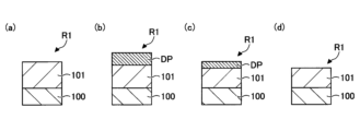
図4は、方法MTのエッチング対象膜の一例を示す断面図である。基板Wは、下地層100、第1領域R1及び第2領域R2を有している。下地層100は、例えば、多結晶シリコンから構成され得る。第1領域R1は酸化シリコン101から形成される。第2領域R2は窒化シリコン102から形成される。
Figure 4 is a cross-sectional view showing an example of a film to be etched by method MT. The substrate W has an
かかる構成の膜を有する基板Wを準備し、図3のプラズマ処理装置10のチャンバ12内に搬送し、載置台14に載置する。プラズマ処理装置10は、方法MTによるエッチングを実行する。方法MTは、基板Wの第1領域R1を第2領域R2に対して選択的にエッチングするために実行される。
A substrate W having such a film is prepared, transported into the
以下、図4に示す対象膜を有する基板Wに方法MTが適用される場合を例として説明する。方法MTでは、プラズマ処理装置10が用いられる。図3においては、一実施形態のプラズマ処理装置10が、鉛直方向に延びる面において部分的に破断された状態で示されている。
The following describes an example in which method MT is applied to a substrate W having a target film as shown in FIG. 4. In method MT, a
図3に示すプラズマ処理装置10は、チャンバ12を備えている。チャンバ12は、略円筒形状を有しており、側壁12a及び底部12bを含んでいる。チャンバ12は、内部空間12sを提供している。図3に示す中心軸線AXは、チャンバ12及び内部空間12sの中心軸線である。チャンバ12は、例えばアルミニウムといった金属から形成されている。チャンバ12の内壁面には、耐プラズマ性を有する膜が形成されている。この膜は、アルマイト膜、酸化イットリウム製の膜といったセラミック製の膜であり得る。チャンバ12は接地されている。
The
側壁12aには、通路12pが形成されている。基板Wは、内部空間12sとチャンバ12の外部との間で搬送されるときに、通路12pを通過する。基板Wは、略円盤形状を有し得る。通路12pは、ゲートバルブ12gによって開閉可能となっている。ゲートバルブ12gは、側壁12aに沿って設けられている。
A
内部空間12sの中には、載置台14が設けられている。載置台14は、支持体15によって支持されている。支持体15は、略円筒形状を有しており、チャンバ12の底部12bから上方に延びている。支持体15は、絶縁性を有しており、例えばセラミックから形成されている。
A mounting table 14 is provided in the
載置台14は、基板Wを支持するように構成されている。載置台14は、チャンバ12と中心軸線AXを共有している。載置台14は、載置領域14rを提供している。この載置領域14rの中心は、中心軸線AX上に位置する。基板Wは、その中心が中心軸線AX上に位置するように、載置領域14r上に載置される。
The mounting table 14 is configured to support a substrate W. The mounting table 14 shares a central axis AX with the
載置台14は、電極プレート16、下部電極18、及び静電チャック20を含んでいる。電極プレート16は、略円盤形状を有している。電極プレート16は、導電性を有している。電極プレート16は、アルミニウムといった金属から形成されている。下部電極18は、略円盤形状を有している。下部電極18は、導電性を有している。下部電極18は、アルミニウムといった金属から形成されている。下部電極18は、電極プレート16上に搭載されている。下部電極18は、電極プレート16に電気的に接続されている。下部電極18を含む載置台14は、チャンバ12内にて基板を載置する第1電極の一例である。
The mounting table 14 includes an
下部電極18の中には、流路18pが形成されている。流路18pは、下部電極18の中で、例えば渦巻状に延びている。流路18pには、熱交換媒体の循環装置22(例えばチラーユニット)から熱交換媒体(例えば温調媒体)が供給される。循環装置22は、チャンバ12の外部に設けられている。流路18pに供給された熱交換媒体は、循環装置22に戻される。熱交換媒体と下部電極18との熱交換により、載置台14上に載置された基板Wの温度が制御される。
A
静電チャック20は、下部電極18上に設けられている。静電チャック20は、略円盤形状を有している。静電チャック20は、セラミック製の本体の中に、膜状の電極を有している。静電チャック20の電極には、スイッチを介して直流電源24が接続されている。静電チャック20は、載置領域14rを提供している。基板Wが静電チャック20上(載置領域14r上)に載置されている状態で、直流電源24からの直流電圧が静電チャック20の電極に印加されると、基板Wと静電チャック20との間で静電引力が発生する。発生した静電引力によって、基板Wは静電チャック20に引き付けられ、静電チャック20によって保持される。プラズマ処理装置10には、静電チャック20と基板Wの下面との間に伝熱ガス(例えばHeガス)を供給する伝熱ガス供給ラインが設けられてもよい。また、静電チャック20の内部には、ヒータ(例えば抵抗加熱素子)が設けられてもよい。ヒータに電力が供給されることによりヒータが発熱し、静電チャック20の温度、ひいては基板Wの温度が調整される。
The
チャンバ12の内部空間12sの中では、エッジリングFRが、静電チャック20及び基板Wのエッジを囲むように配置される。エッジリングFRは、環状の板であり、シリコン、石英といったシリコン含有材料から形成されている。エッジリングFRは、プラズマ処理の均一性を得るために利用され、フォーカスリングともいう。
In the
支持体15の周りには、筒状の導体26が設けられている。導体26は接地されている。導体26の上方には、載置台14を囲むように筒状の絶縁体28が設けられている。絶縁体28は、石英といったセラミックから形成されている。載置台14とチャンバ12の側壁12aとの間には、排気路が形成されている。排気路には、バッフルプレート30が設けられている。バッフルプレート30は、環状の板である。バッフルプレート30には、バッフルプレート30をその板厚方向に貫通する多数の孔が形成されている。バッフルプレート30は、アルミニウムといった金属から形成された母材の表面に、酸化イットリウムといった耐プラズマ性の被膜を形成することにより構成されている。
A
バッフルプレート30の下方では、排気管32がチャンバ12の底部12bに接続されている。排気管32は、排気路に連通可能である。排気管32には、排気装置34が接続されている。排気装置34は、自動圧力制御弁、及びターボ分子ポンプといった減圧ポンプを含んでいる。排気装置34が作動されることにより、内部空間12sの圧力が指定された圧力に設定される。
Below the
載置台14の上方には、上部電極36が設けられている。上部電極36と載置台14との間には、内部空間12sの一部が介在している。上部電極36は、チャンバ12の上部開口を閉じるように設けられている。上部電極36とチャンバ12の上端部との間には部材37が介在している。部材37は、絶縁性材料から形成されている。部材37は、セラミック、例えば石英から形成され得る。なお、一実施形態では、上部電極36とチャンバ12の上端部との間には、部材37及び接地導体50の一部が介在し得る。
An
一実施形態において、上部電極36は、シャワーヘッドを構成している。上部電極36は、基板を載置する第1電極に対向する第2電極の一例である。上部電極36は、一実施形態では、天板38及び天板支持体40を含んでいる。天板38は、例えばシリコンから形成されている。或いは、天板38は、アルミニウムから形成された母材の表面に、酸化イットリウムといったセラミックから形成された被膜を設けることにより構成される。天板38には、当該天板38をその板厚方向に貫通する複数のガス吐出口38hが形成されている。
In one embodiment, the
天板支持体40は、天板38上に設けられている。天板支持体40は、天板38を着脱自在に支持するように構成されている。天板支持体40は、アルミニウムといった導電性材料から形成されている。天板支持体40の内部には、ガス拡散室40dが形成されている。天板支持体40には、ガス拡散室40dから下方に延びる複数の孔40hが形成されている。複数の孔40hはそれぞれ、複数のガス吐出口38hに連通している。
The
ガス拡散室40dには、ガス供給部41が接続されている。ガス供給部41は、内部空間12sにガスを供給するように構成されている。ガス供給部41は、方法MTにおいて用いられる複数のガスを出力可能に構成されている。また、ガス供給部41は、複数の流量制御器及び複数のバルブを有し、出力すべきガスの流量を個別に調整するように構成されている。ガス供給部41から出力されたガスは、ガス拡散室40d及び複数の孔40hを介して、複数のガス吐出口38hから内部空間12sに吐出される。
A
天板支持体40には、流路40pが形成されている。流路40pには、チラーユニット42が接続されている。流路40pとチラーユニット42との間では、冷却水といった温調媒体が循環される。チラーユニット42から流路40pに供給される温調媒体と上部電極36との間の熱交換により、上部電極36の温度が調整される。
A
プラズマ処理装置10は、第1の高周波電源43及び第2の高周波電源44を更に備えている。第1の高周波電源43及び第2の高周波電源44は、チャンバ12の外部に設けられている。第1の高周波電源43は、主としてプラズマ生成用の高周波電力を発生するよう構成されている。プラズマ生成用の高周波電力の第1の高周波は、限定されるものではないが、例えば60MHzといった周波数を有し得る。第1の高周波電源43は、整合器45及び給電導体48を介して、上部電極36に電気的に接続されている。整合器45は、第1の高周波電源43の出力インピーダンスと負荷側(上部電極36側)のインピーダンスとを整合させるための整合回路を有している。給電導体48は、その下端で上部電極36に接続されている。給電導体48は、上部電極36から上方に延びている。給電導体48は筒状又は棒状の導体であり、その中心軸線は中心軸線AXに略一致している。
The
第2の高周波電源44は、主として基板Wにイオンを引き込むためのバイアス用の高周波電力を発生するように構成されている。バイアス用の高周波電力の第2の高周波の周波数は、第1の高周波の周波数よりも低い。一実施形態では、第2の高周波の周波数は、40MHz以上であってもよい。第2の高周波電源44は、整合器46を介して、下部電極18に電気的に接続されている。整合器46は、第2の高周波電源44の出力インピーダンスと負荷側(下部電極18側)のインピーダンスとを整合させるための整合回路を有している。
The second high
なお、第1の高周波電源43は、高周波電力を上部電極36に印加する替わりに下部電極18に印加してもよい。第1の高周波電源43及び第2の高周波電源44は、いずれもプラズマ生成用の高周波電力を供給するプラズマ生成部になり得る。
The first high
プラズマ処理装置10は、接地導体50を更に備えている。接地導体50は、導電性を有する。接地導体50は、アルミニウムといった金属から形成されている。接地導体50は、接地されている。接地導体50は、チャンバ12の上方で上部電極36を覆うように延びている。給電導体48は、接地導体50によって囲まれた空間を通って接地導体50の外部まで上方へ延びて、接地導体50の外部で整合器45を介して第1の高周波電源43に接続されている。
The
プラズマ処理装置10のチャンバ12の内部空間12sの中では、基板Wの中心の上では高い電界強度を有し、基板Wのエッジ側の上では低い電界強度を有する電界強度の分布が形成され得る。即ち、内部空間12sの中では、放射方向(即ち、径方向)における中心軸線AXからの距離の増加に応じて電界強度が減少する不均一な電界強度の分布が形成され得る。不均一な電界強度の分布の下では、プラズマ密度は、中心軸線の近傍で高く、中心軸線から離れた箇所で低くなる。即ち、中心軸線に対して放射方向において不均一なプラズマ密度の分布が形成される。プラズマ処理装置10は、均一なプラズマ密度の分布を得るために、電磁石60を更に備えている。
In the
電磁石60は、上部電極36の上方に配置されている。電磁石60は、チャンバ12の内部空間12sの中で、中心軸線AX上での水平成分よりも大きい水平成分を中心軸線AXから離れた位置で有する磁場の分布を形成する。即ち、電磁石60は、中心軸線AXから放射方向への距離の増加に応じてその大きさが増加する水平成分を有する磁場の分布を、内部空間12sの中に形成する。大きい水平成分の磁場が形成されている箇所では、電子の滞在時間が長くなる。その結果、大きい水平成分の磁場が形成されている箇所では、プラズマの密度が上昇する。したがって、プラズマ処理装置10によれば、中心軸線AXに対して放射方向において均一なプラズマ密度の分布が得られる。故に、プラズマ処理装置10によれば、基板Wに対する処理の面内均一性が向上される。
The
一実施形態では、電磁石60は、ヨーク62及びコイル64を有している。ヨーク62は、磁性材料から形成されている。ヨーク62は、ベース部62a及び複数の筒状部62bを有している。ベース部62aは、略円盤形状を有しており、中心軸線AXに対して直交する方向に延在している。複数の筒状部62bの各々は、筒形状を有しており、ベース部62aから下方に延在している。複数の筒状部62bは、中心軸線AXに対して同軸状に設けられている。コイル64は、中心軸線AXの周りで巻かれている。コイル64は、径方向において隣り合う二つの筒状部62bの間に設けられている。なお、電磁石60は、一以上のコイル64を有し得る。電磁石60におけるコイル64の個数が複数個である場合には、複数個のコイル64は、中心軸線AXに対して同軸状に設けられる。
In one embodiment, the
電磁石60のコイル64は、配線68を介して電流源66に接続されている。電流源66からの電流がコイル64に与えられると、電磁石60によって磁場が形成される。電磁石60によって形成される磁場のベクトルの角度が45°である箇所では、放射方向(径方向)における電子の閉じ込め効果(電子の拡散の抑制効果)と、電子の消滅の抑制効果(電極への電子の到達を抑制する効果)とが良好に両立される。このため、当該箇所ではプラズマの密度が高くなる。したがって、基板Wの半径が150mmである場合に、電磁石60は、磁場のベクトルの角度が45°である箇所と中心軸線AXとの間の距離が、135mm以上、185mm以下となるように、構成され得る。
The
電磁石60は、接地導体の外側に配置される。接地導体50は、その中に電磁石60が配置される外部空間ESを提供している。外部空間ESは、接地導体50の上端よりも内部空間12sの側にあり、上部電極36に対して上方に離れており、且つ、上部電極36に対して接地導体50により遮蔽されている。
The
接地導体50は、第1の部分51、第2の部分52、及び第3の部分53を備えている。第1の部分51は、筒形状を有している。第1の部分51の中心軸線は、中心軸線AXと略一致している。第1の部分51は、チャンバ12から上方に延びている。図3に示す例では、第1の部分51は、チャンバ12の側壁12aの上端から上方に延びている。第1の部分51の下端部分は、部材37と側壁12aの上端との間に介在している。
The
第2の部分52は、上部電極36から上方に離間し、且つ、第1の部分51から中心軸線AXに向けて延びている。第2の部分52は、中心軸線AXに対して交差又は直交する方向に延びる板状をなしている。第1の部分51と第2の部分52は、上部電極36の上に第1の空間IS1を提供している。第1の空間IS1は、接地導体50の内側(即ち、上部電極36側)の空間の一部である。この第1の空間IS1により、鉛直方向において上部電極36と接地導体50との間に距離が確保される。したがって、接地導体50と上部電極36との間の容量的結合が抑制される。
The second portion 52 is spaced upward from the
第3の部分53は、筒形状を有している。第3の部分53の中心軸線は、中心軸線AXと略一致している。第3の部分53は、第1の部分51よりも中心軸線の近くで延在している。第3の部分53は、第2の部分52から上方に延びている。第3の部分53は、第2の空間IS2を提供している。第2の空間IS2は、第2の部分52の内側の空間であり、接地導体50の内側(即ち、上部電極36側)の空間の一部である。第2の空間IS2は、第1の空間IS1に連続している。なお、給電導体48は、第1の空間IS1及び第2の空間IS2を通って上方に延びている。
The
外部空間ESは、第3の部分53の外側、第2の部分52上、且つ、内部空間12sの上方に接地導体50によって提供されている。外部空間ESは、第3の部分53の外側、且つ、第2の部分52上で、中心軸線AXを中心に周方向に延びている。この外部空間ESに電磁石60が配置されている。
The external space ES is provided by the
外部空間ESの中に配置された電磁石60と内部空間12sとの間の距離は比較的短い。また、上述したように、電磁石60は、中心軸線AXの近傍では低い水平成分を有し、中心軸線から離れた位置で大きい水平成分を有する磁場の分布を内部空間12sの中に形成する。したがって、接地導体50に対して外側に配置された電磁石60によって、均一なプラズマ密度の分布を得るのに適した磁場の分布が効率的に内部空間12sの中に形成され得る。
The distance between the
電磁石60のコイル64には、上述したように電流源66が接続されている。電磁石60及び電流源66は、接地導体50に対して外側に配置されている。したがって、電流源66への高周波の流入を防止するためのフィルタが、コイル64と電流源66との間に設けられていなくてもよい。
As described above, the
一実施形態では、接地導体50は、第4の部分54、第5の部分55、及び第6の部分56を更に有する。第4の部分54は、第2の部分52の上方で、中心軸線AXに対して放射方向に第3の部分53から延びている。第4の部分54は、中心軸線AXに対して交差又は直交する方向に延びる板状をなしている。第5の部分55は、筒形状を有している。第5の部分55の中心軸線は、中心軸線AXに略一致している。第5の部分55は、第3の部分53よりも中心軸線から離れており、第4の部分54から上方に延びている。第6の部分56は、第4の部分54の上方で、第5の部分55から中心軸線AXに向けて延びている。第6の部分56は、中心軸線AXに対して交差又は直交する方向に延びる板状をなしている。一実施形態では、接地導体50は、第6の部分から給電導体48の近傍まで延びる蓋部57を更に有している。
In one embodiment, the
第4の部分54、第5の部分55、及び第6の部分56は、第3の空間IS3を提供している。第3の空間IS3は、第4の部分54、第5の部分55、及び第6の部分56によって囲まれた空間であり、接地導体50の内側の空間の一部である。第3の空間IS3は、第2の空間IS2に連続している。給電導体48は、第3の空間IS3を更に通って、上方に延びている。なお、図3に示す例では、第1~第6の部分は、三つの部材で構成されているが、接地導体50を構成する部材の個数は、任意の個数であり得る。
The
一実施形態において、プラズマ処理装置10は、管71を更に備えている。管71は、上部電極36から、第1の空間IS1及び第2の空間IS2を通って上方に延び、第3の空間IS3を通って、接地導体50に対して側方且つ外側まで延びている。管71は、接地導体50に対して外側で、チラーユニット42に接続される。チラーユニット42からの温調媒体は、管71を介して、流路40pに供給される。第3の空間IS3内では、管71が、接地導体50の第4の部分54によって上部電極36から実質的に遮蔽されている。
In one embodiment, the
一実施形態において、プラズマ処理装置10は、管73を更に備えている。管73は、上部電極36から、第1の空間IS1及び第2の空間IS2を通って上方に延び、第3の空間IS3を通って、接地導体50に対して側方且つ外側まで延びている。管73は、接地導体50に対して外側で、ガス供給部41に接続されている。ガス供給部41から出力されるガスは、管73を介して、上部電極36、即ちシャワーヘッドに供給される。第3の空間IS3内では、管73が、接地導体50の第4の部分54によって上部電極36から実質的に遮蔽されている。なお、ガス供給部41と上部電極36(即ち、シャワーヘッド)は、複数の管を介して互いに接続されていてもよい。
In one embodiment, the
一実施形態において、プラズマ処理装置10は直流電源74を更に備えている。直流電源74は、上部電極36に印加される負極性の直流電圧を発生するよう構成されている。直流電源74と上部電極36とを互いに接続している配線(図示しない)は、コイル75cを含み得る。コイル75cは、第3の空間IS3の中に設けられている。直流電源74と上部電極36とを互いに接続している配線は、上部電極36から第1の空間IS1及び第2の空間IS2を通って上方に延び、第3の空間IS3を通って、接地導体50に対して側方且つ外側まで延びている。
In one embodiment, the
一実施形態において、プラズマ処理装置10は、制御部80を更に備えている。制御部80は、プラズマ処理装置10の各部を制御するように構成されている。制御部80は、コンピュータ装置であり得る。制御部80は、プロセッサ、メモリといった記憶装置、キーボード、マウス、タッチパネルといった入力装置、表示装置、制御信号の入出力インタフェイス等を有し得る。記憶装置には、制御プログラム及びレシピデータが記憶されている。制御部80のプロセッサは、制御プログラムを実行し、レシピデータに従って、プラズマ処理装置10の各部を制御するために制御信号を送出する。制御部80は、一実施形態に係る方法MTを実行のために、プラズマ処理装置10の各部を制御する。
In one embodiment, the
[エッチング方法]
次に、プラズマ処理装置10にて実行可能な方法MTについて説明する。方法MTの実行時のプラズマ処理装置10の各部の動作は、制御部80によって制御され得る。方法MTでは、まず、図2のステップS1において、載置台14に、第1領域R1と第2領域R2を有する基板Wを準備する。次に、ステップS2において、基板の表面状態のモニタを開始する。方法MT中にエッチングにより生成される副生成物が第1領域R1及び第2領域R2に付着し、堆積物となる。ステップS2ではこの堆積物の厚さを制御部80によりモニタする。モニタ方法は、基板Wに照射する光の反射により堆積物の厚さを測定可能な測定装置を使用して実行することができる。ただし、堆積物の厚さの測定は、これに限られず、その他の公知の方法により実行してもよい。
[Etching method]
Next, a method MT that can be performed by the
次に、ステップS3において、フルオロカーボンガスを含む第1の処理ガスが供給される。フルオロカーボンガスは、例えば、C4F6ガス及びC4F8ガスのうち少なくとも一種を含む。また、第1の処理ガスは、アルゴン(Ar)ガス、ヘリウム(He)ガスといった種々の希ガスのうち少なくとも一種を含み得る。さらに、この処理ガスは、酸素(O2)ガスを含み得る。ステップS3では、第1の処理ガスが励起されることによりプラズマが生成され、生成されたプラズマに基板Wが晒される。 Next, in step S3, a first process gas containing a fluorocarbon gas is supplied. The fluorocarbon gas may contain at least one of C4F6 gas and C4F8 gas. The first process gas may also contain at least one of various rare gases such as argon (Ar) gas and helium (He) gas. Furthermore, the process gas may also contain oxygen ( O2 ) gas. In step S3, the first process gas is excited to generate plasma, and the substrate W is exposed to the generated plasma.
プラズマ処理装置10を用いてステップS3を実施する場合には、ガス供給部41から第1の処理ガスがチャンバ12内に供給される。また、第1の高周波電源43からのプラズマ生成用の高周波電力が上部電極36に供給される。また、第2の高周波電源44からのバイアス用の高周波電力が下部電極18に供給され得る。また、排気装置34によってチャンバ12内の空間の圧力が所定の圧力に設定される。例えば、チャンバ12内の空間の圧力は、10mTorr(1.333Pa)~50mTorr(6.666Pa)の範囲内の圧力に設定される。
When step S3 is performed using the
ステップS3では、初期的には図4に示す基板Wの第1領域R1に、フルオロカーボンに由来する原子及び/又は分子の活性種、例えば、フッ素及び/又はフルオロカーボンの活性種が衝突する。これにより、ステップS3では、第1領域R1がエッチングされる。また、ステップS3では、フルオロカーボンを含む堆積物が第1領域R1に付着する。これにより、フルオロカーボンを含む堆積物DPが第1領域R1上に形成される。この堆積物DPの膜厚は、ステップS3の実行時間の経過につれて増加する。 In step S3, initially, active species of atoms and/or molecules derived from fluorocarbon, for example, active species of fluorine and/or fluorocarbon, collide with the first region R1 of the substrate W shown in FIG. 4. As a result, the first region R1 is etched in step S3. Also, in step S3, a deposit containing fluorocarbon adheres to the first region R1. As a result, a deposit DP containing fluorocarbon is formed on the first region R1. The film thickness of this deposit DP increases as the execution time of step S3 elapses.
図5は、方法MTによる第1領域R1のエッチングを説明するための図である。図5(a)は第1領域R1の初期状態である。これに対して、ステップS3では、図5(b)に示すように、第1領域R1はプラズマ中のフルオロカーボンの活性種によってエッチングされ、また、第1領域R1上にはフルオロカーボンの活性種によってフルオロカーボンの堆積物DPが形成される。 Figure 5 is a diagram for explaining the etching of the first region R1 by method MT. Figure 5(a) shows the initial state of the first region R1. In contrast, in step S3, as shown in Figure 5(b), the first region R1 is etched by active fluorocarbon species in the plasma, and a fluorocarbon deposit DP is formed on the first region R1 by the active fluorocarbon species.
ステップS3では、初期的には図4の第2領域R2にも、フルオロカーボンに由来する原子及び/又は分子の活性種、例えば、フッ素及び/又はフルオロカーボンの活性種が衝突する。図6は、方法MTによる第2領域R2のエッチングを説明するための図である。 In step S3, initially, the second region R2 in FIG. 4 is also bombarded with active species of atoms and/or molecules derived from fluorocarbons, such as active species of fluorine and/or fluorocarbons. FIG. 6 is a diagram for explaining the etching of the second region R2 by method MT.
かかる活性種が第2領域R2に衝突すると、図6(a)の初期状態に対して図6(b)に示すように、第2領域R2の表面にフルオロカーボン堆積物が変質したカーボン含有比率の高い変質領域TRが形成される。また、その上にカーボン及びシリコンを含有した堆積物DPが積層される。変質領域TRは、第2領域R2を構成するシリコン及び窒素、処理ガスに含まれる原子及び/又は分子を含有し、窒化シリコン102がエッチングされることを抑制する。例えば、変質領域TRは、シリコン及び窒素に加えて、処理ガスに含まれる炭素、フッ素、及び酸素を含有し得る。
When such active species collide with the second region R2, as shown in FIG. 6(b) in comparison with the initial state in FIG. 6(a), a fluorocarbon deposit is transformed on the surface of the second region R2 to form a transformed region TR with a high carbon content. A deposit DP containing carbon and silicon is also layered on top of the transformed region TR. The transformed region TR contains the silicon and nitrogen that constitute the second region R2, and the atoms and/or molecules contained in the processing gas, and suppresses the etching of the
ステップS3の処理により形成された堆積物DPの膜厚が大きくなると、第1領域R1をエッチングし得る活性種が第1領域R1に到達することが当該堆積物DPによって阻害される。したがって、ステップS3を連続的に継続すると、第1領域R1のエッチングが停止する。このようなエッチングの停止を防止するために、方法MTでは、次いで、図2のステップS4が実行される。 When the thickness of the deposit DP formed by the processing of step S3 increases, the deposit DP prevents active species capable of etching the first region R1 from reaching the first region R1. Therefore, if step S3 is continued continuously, the etching of the first region R1 will stop. To prevent such etching from stopping, the method MT then performs step S4 in FIG. 2.
ステップS4では、堆積物DPに含まれるフルオロカーボンのラジカルにより第1領域R1がエッチングされる。一実施形態のステップS4では、ステップS3の処理後の基板Wが、Arガス等の希ガスのプラズマに晒される。このステップS4のエッチング処理時間とステップS3の処理時間は任意に設定され得る。一実施形態においては、ステップS3の処理時間とステップS4のエッチング処理時間の合計においてステップS3の処理時間が占める割合は、30%~70%の範囲内の割合に設定され得る。 In step S4, the first region R1 is etched by fluorocarbon radicals contained in the deposit DP. In one embodiment, in step S4, the substrate W after processing in step S3 is exposed to a plasma of a rare gas such as Ar gas. The etching processing time of step S4 and the processing time of step S3 can be set arbitrarily. In one embodiment, the proportion of the processing time of step S3 in the total processing time of step S3 and the etching processing time of step S4 can be set to a proportion within the range of 30% to 70%.
プラズマ処理装置10を用いてステップS4を実施する場合には、ガス供給部41からArガス等の希ガスが供給される。また、ステップS4では、希ガスに加えて酸素ガス(O2ガス)が供給されてもよく、或いは、酸素ガスが供給されなくてもよい。また、ステップS4では、第1の高周波電源43からのプラズマ生成用の高周波電力が上部電極36に供給され、第2の高周波電源44からのバイアス用の高周波電力が下部電極18に供給され得る。ステップS4において出力されるプラズマ生成用の高周波電力は、ステップS3において出力されるプラズマ生成用の高周波電力と同じであってもよいし、高くてもよい。ステップS4において、ステップS3よりも高周波電力を高くすると、イオンフラックスを増やすことができる。
When step S4 is performed using the
一方、ステップS4において出力されるバイアス用の高周波電力は、ステップS3において出力されるバイアス用の高周波電力よりも高くすることが好ましい。これにより、プラズマ中のイオンの引き込みを高め、エッチングの効果を高めることができる。 On the other hand, it is preferable that the bias high frequency power output in step S4 is higher than the bias high frequency power output in step S3. This can increase the attraction of ions into the plasma and improve the etching effect.
また、ステップS4では、排気装置34によってチャンバ12内の空間の圧力が所定の圧力に設定される。例えば、チャンバ12内の空間の圧力は、10mTorr(1.333Pa)~50mTorr(6.666Pa)の範囲内の圧力に設定される。
In addition, in step S4, the pressure in the space within the
チャンバ12内においてArガス等の希ガスのプラズマが生成され、載置台14上に載置された基板Wが希ガスのプラズマに晒される。ステップS4では、希ガス原子の活性種、例えば、希ガス原子のイオンが、堆積物DPに衝突する。これにより、図5(c)に示すように、堆積物DP中のフルオロカーボンラジカルが、第1領域R1のエッチングを進行させる。また、このステップS4により、堆積物DPの膜厚が減少する。また、ステップS4では、図6(c)に示すように、第2領域R2上の堆積物DPの膜厚も減少する。ただし、第2領域R2上には変質領域TRが存在するので、第2領域R2のエッチングは抑制される。これにより、第1領域R1が第2領域R2に対して選択的にエッチングされる。なお、ステップS4において酸素ガスが供給されない場合には、第1領域R1が第2領域R2に対して更に選択的にエッチングされ得る。
In the
次に、図2のステップS5では、停止条件として例えばステップS3及びS4のサイクルの繰り返し回数が所定回数に達したかを判定し、所定回数に達したときに停止条件が満たされたものと判定される。停止条件が満たされない場合には、ステップS6が実行される。一方、停止条件が満たされる場合には、本処理が終了する。 Next, in step S5 of FIG. 2, a determination is made as to whether the number of repetitions of the cycle of steps S3 and S4 has reached a predetermined number as a stop condition, and when the predetermined number of repetitions has been reached, it is determined that the stop condition has been met. If the stop condition is not met, step S6 is executed. On the other hand, if the stop condition is met, this process ends.
ステップS6では、ステップS2において測定した堆積物DPの厚さが予め定められた閾値以上であるかを判定する。方法MTでは、基板Wの表面状態をモニタして堆積物DPの膜厚をリアルタイムに測定する。これにより、より効果的に堆積物DPを除去することができる。ステップS6において堆積物DPの厚さが閾値以上である場合、ステップS7において、酸素を含まない第2の処理ガスを供給し、第2の処理ガスのプラズマにより堆積物DPを除去する。 In step S6, it is determined whether the thickness of the deposit DP measured in step S2 is equal to or greater than a predetermined threshold. In method MT, the surface condition of the substrate W is monitored to measure the thickness of the deposit DP in real time. This makes it possible to remove the deposit DP more effectively. If the thickness of the deposit DP is equal to or greater than the threshold in step S6, a second process gas not containing oxygen is supplied in step S7, and the deposit DP is removed by plasma of the second process gas.
ステップS3及びステップS4のエッチング処理を繰り返し行うと、第1領域R1のエッチングの停止が生じることがある。そこで、堆積物DPの厚さが閾値以上である場合、エッチングの停止が生じる可能性があると判定し、ステップ7において酸素を含まない第2の処理ガスのプラズマにより堆積物DPを除去する工程を実行する。
When the etching processes of steps S3 and S4 are repeated, etching of the first region R1 may stop. Therefore, if the thickness of the deposit DP is equal to or greater than a threshold value, it is determined that etching may stop, and in
第2の処理ガスは、フッ素含有ガスのうち少なくとも一種、又は窒素(N2)ガスを含む。フッ素含有ガスは、例えば、四フッ化メタン(CF4)ガス、三フッ化窒素(NF3)ガス及び六フッ化硫黄(SF6)ガスのうち少なくとも一種であってもよい。第2の処理ガスにCxFyガスを使用することはできない。CxFyガスを使用するとカーボンを含む堆積物DPが堆積し過ぎるためである。 The second process gas contains at least one of fluorine-containing gases or nitrogen ( N2 ) gas. The fluorine-containing gas may be at least one of tetrafluoromethane ( CF4 ) gas, nitrogen trifluoride ( NF3 ) gas, and sulfur hexafluoride ( SF6 ) gas. CxFy gas cannot be used for the second process gas. This is because excessive carbon-containing deposits DP are deposited if CxFy gas is used.
第2の処理ガスは、アルゴン(Ar)ガス、ヘリウム(He)ガスといった種々の希ガスのうち少なくとも一種を含み得るが、第2の処理ガスに水素(H2)ガスを使用することはできない。水素ガスを使用すると、水素ガスのプラズマが保護膜を通過して窒化シリコン102にまで到達し、窒化シリコン102の膜の表面が改質され、窒化シリコン102膜が劣化するためである。
The second process gas may contain at least one of various rare gases such as argon (Ar) gas and helium (He) gas, but hydrogen (H 2 ) gas cannot be used for the second process gas, because if hydrogen gas is used, the hydrogen gas plasma will pass through the protective film and reach the
第2の処理ガスは、酸素(O2)ガスを含まない。ステップ7の堆積物DPを除去する工程(以下、「除去工程」ともいう。)は、図5(c)に示す堆積物DPの厚さが閾値以上の場合に実行され、図5(d)に示すように、領域R1の堆積物DPが除去される。これにより、酸化シリコン101の第1領域R1のエッチングの停止を回避できる。
The second process gas does not contain oxygen (O 2 ) gas. The process of removing the deposit DP in step 7 (hereinafter also referred to as the "removal process") is performed when the thickness of the deposit DP shown in Fig. 5C is equal to or greater than a threshold value, and the deposit DP in the region R1 is removed as shown in Fig. 5D. This makes it possible to avoid stopping the etching of the first region R1 of the
このようにステップS7の除去工程では、酸化シリコン101の堆積物DPを除去する間、領域R2の窒化シリコン102も第2の処理ガスに晒される。このとき、第2の処理ガスに酸素ガスが含まれると、窒化シリコン102は酸化し、ダメージを受けて劣化してしまう。
In this way, in the removal process of step S7, while removing the
図7は、第2領域R2の状態を説明するための図である。図7(a)では、堆積物DPを除去する工程において、酸素ガスを含んだ処理ガスを供給した場合の第2領域R2の状態を模式的に示す。この場合、プラズマ中のフルオロカーボンのラジカル(CFx
*)だけでなく酸素ガスのラジカル(O*)が供給され、酸素ガスのラジカル(O*)によって、窒化シリコン102の表層が酸化し、劣化する。
7A and 7B are diagrams for explaining the state of the second region R2. Fig. 7A shows a schematic diagram of the state of the second region R2 when a processing gas containing oxygen gas is supplied in the process of removing the deposit DP. In this case, not only fluorocarbon radicals ( CFx * ) in the plasma but also oxygen gas radicals (O * ) are supplied, and the surface layer of the
そこで、方法MTでは、第2の処理ガスに酸素ガスを含まない。これにより、図7(b)に示すように、窒化シリコン102の酸化を防ぐ。この結果、MT方法では、ステップS7において、図5(d)に示すように、領域R1の酸化シリコン101の堆積物DPを除去しつつ、図6(d)及び図7(b)に示すように、窒化シリコン102の酸化を防止することができる。これにより、酸化シリコン101の第1領域R1のエッチングの停止を回避し、領域R2の窒化シリコン102の劣化を防止しながら、第1領域R1のエッチングを進行できる。
Therefore, in method MT, the second process gas does not contain oxygen gas. This prevents oxidation of
プラズマ処理装置10を用いてステップS7を実施する場合には、ガス供給部41から第2の処理ガスがチャンバ12内に供給される。また、第1の高周波電源43からのプラズマ生成用の高周波電力が上部電極36に供給される。第1の高周波電源43からは、例えば周波数が60MHzであって100Wの高周波電力を出力する。また、排気装置34によってチャンバ12内の空間の圧力が所定の圧力に設定される。例えば、チャンバ12内の空間の圧力は、10mTorr(1.333Pa)~50mTorr(6.666Pa)の範囲内の圧力に設定される。
When step S7 is performed using the
ステップS7を実施する場合、第2の高周波電源44からのバイアス用の高周波電力を下部電極18に供給すると、図7(c)に示すように、プラズマ中のフルオロカーボンのラジカル(CFx
*)とともに、フルオロカーボンのイオン(CFx
+)が供給される。このため、イオンエネルギーにより窒化シリコン102が損失する。
When step S7 is performed, when bias high frequency power is supplied from the second high
よって、ステップS7の除去工程では、第1の高周波電源43からのプラズマ生成用の高周波電力のみを上部電極36に供給し、第2の高周波電源44からのバイアス用の高周波電力は下部電極18に供給しない。
Therefore, in the removal process of step S7, only the high frequency power for plasma generation from the first high
このようにしてステップS7の除去工程を実行した後、再び、ステップS3及びステップS4が繰り返し実行される。この場合、先のステップS7の実行によって堆積物DPの膜厚が減少しているので、再びステップS3を実行して上述した処理ガスのプラズマに基板Wを晒すと、第1領域R1を更にエッチングすることができる。その後、更にステップS4が実行することで、堆積物DP中のフルオロカーボンラジカルにより第1領域R1をエッチングすることができる。 After performing the removal process of step S7 in this manner, steps S3 and S4 are repeated again. In this case, since the thickness of the deposit DP has been reduced by performing step S7 previously, step S3 is performed again to expose the substrate W to the plasma of the above-mentioned processing gas, so that the first region R1 can be further etched. Then, step S4 is further performed, so that the first region R1 can be etched by the fluorocarbon radicals in the deposit DP.
ステップS6において、堆積物DPの厚さが予め定められた閾値未満である場合、再び、ステップS3及びステップS4が繰り返し実行される。この場合、先のステップS4の実行によって堆積物DPの膜厚が減少しているので、再びステップS3を実行して上述した処理ガスのプラズマに基板Wを晒すと、第1領域R1を更にエッチングすることができる。その後、更にステップS4が実行することで、堆積物DP中のフルオロカーボンラジカルにより第1領域R1をエッチングすることができる。 If, in step S6, the thickness of the deposit DP is less than a predetermined threshold value, steps S3 and S4 are executed again repeatedly. In this case, the thickness of the deposit DP has been reduced by the previous execution of step S4, so that the first region R1 can be further etched by executing step S3 again and exposing the substrate W to the plasma of the above-mentioned processing gas. Then, step S4 is further executed, so that the first region R1 can be etched by the fluorocarbon radicals in the deposit DP.
なお、ステップ7では、所定量の堆積物DPを減少させることができれば、すべての堆積物DPを除去させなくてもよい。
In
[実験例]
以下、方法MTの評価のために行った種々の実験例について説明する。以下に説明する実験例は単に例示のために示されるものであって、本発明を限定するものではない。
[Experimental Example]
Various experimental examples conducted to evaluate Method MT are described below. The experimental examples described below are presented for illustrative purposes only and are not intended to limit the present invention.
図8は、窒化シリコン102の損失の一例を示す図である。図8の横軸は、後述する図12のSACプロセスにおける酸化シリコン101の凹部の深さ(Slit depth)を示し、縦軸は、窒化シリコン102の損失を示す。
Figure 8 is a diagram showing an example of the loss of
これによれば、除去工程を行わないエッチング方法a(図1に示す比較例)に対して、第2の処理ガスに酸素ガスを含む場合の除去工程を行うエッチング方法b(比較例)は窒化シリコン102の損失が低減した。また、エッチング方法bに対して、方法MTの第2の処理ガスに酸素ガスを含まない場合の除去工程を行うエッチング方法cは、更に窒化シリコン102の損失が低減した。以上から、方法MTの除去工程では、第2の処理ガスに酸素ガスを含まないことで、窒化シリコン102の損失を低減させることができた。
According to this, compared to etching method a (comparative example shown in FIG. 1) which does not perform a removal step, etching method b (comparative example) which performs a removal step when the second processing gas contains oxygen gas reduced the loss of
図9は、方法MTによる除去工程(図2 S7)後のエッチング(図2 S3、S4)におけるCOの発光強度を測定した結果の一例を比較例と比較して示した図である。図9の横軸は、エッチング時間を示し、縦軸は、COの発光強度を示す。 Figure 9 shows an example of the results of measuring the CO emission intensity during etching (Figure 2, S3, S4) after the removal step (Figure 2, S7) by method MT, in comparison with a comparative example. The horizontal axis of Figure 9 shows the etching time, and the vertical axis shows the CO emission intensity.
方法MTのCF4ガスを含み、酸素ガスを含まない第2の処理ガスによる除去工程を実行したエッチング方法B、除去工程を実行しないエッチング方法A(図1の比較例)、及びO含有ガスによる除去工程を実行したエッチング方法C~E(比較例)を比較した。その結果、エッチング方法C~Eでは、O含有ガスを用いたために不要な酸化膜が形成され、COの発光強度が高くなった。一方、方法MTのCF4ガスによる除去工程を実行したエッチング方法Bでは、除去工程に酸素を含まないガスを使用するために不要な酸化膜が形成されず、COの発光強度が、除去工程を実行しないエッチング方法Aと同程度に低くなった。 The etching method B, which includes the removal step using the second processing gas containing CF4 gas and not containing oxygen gas in the method MT, the etching method A (comparative example in FIG. 1) which does not include the removal step, and the etching methods C to E (comparative examples) which include the removal step using an O-containing gas were compared. As a result, in the etching methods C to E, an unnecessary oxide film was formed because an O-containing gas was used, and the emission intensity of CO was high. On the other hand, in the etching method B, which includes the removal step using CF4 gas in the method MT, an unnecessary oxide film was not formed because a gas not containing oxygen was used in the removal step, and the emission intensity of CO was as low as that of the etching method A which does not include the removal step.
図10は、除去工程におけるバイアス用の高周波電力の有無と窒化シリコン及び堆積物DPのエッチングレートの関係を示す図である。図10(a)は、第1の高周波電源43から100Wのプラズマ生成用の高周波電力を上部電極36に供給し、第2の高周波電源44からのバイアス用の高周波電力を供給しない場合の窒化シリコン102及び堆積物DPのエッチングレートを示す。
Figure 10 shows the relationship between the presence or absence of bias high frequency power in the removal process and the etching rate of silicon nitride and deposit DP. Figure 10(a) shows the etching rate of
図10(b)は、第1の高周波電源43から100Wのプラズマ生成用の高周波電力を上部電極36に供給し、第2の高周波電源44から100Wのバイアス用の高周波電力を供給した場合の窒化シリコン102及び堆積物DPのエッチングレートを示す。
Figure 10(b) shows the etching rate of
これによれば、MT方法の除去工程において、第2の高周波電源44からのバイアス用の高周波電力を下部電極18に供給すると、イオンエネルギーにより、堆積物DPのエッチングレートが向上するが、窒化シリコン102の損失を招いた。これに対して、バイアス用の高周波電力を下部電極18に供給しない場合、バイアス用の高周波電力を供給した場合と比べて堆積物DPのエッチングレートは下がるものの、窒化シリコン102の損失を防ぐことができた。
According to this, when bias high frequency power from the second high
図11は、除去工程の処理時間と酸化シリコンのエッチングレートの関係を示す図である。図11(a)は、除去工程を行わないエッチング方法(図1に示す比較例)の場合、図11(b)及び(c)は除去工程を行う方法MTの場合の酸化シリコン101のエッチングレートを示す。図11(b)の除去工程の処理時間は5秒、図11(c)の除去工程の処理時間は30秒であった。
Figure 11 shows the relationship between the processing time of the removal step and the etching rate of silicon oxide. Figure 11(a) shows the etching rate of
図11の各グラフの横軸は直径が300mmの基板の位置(X軸及びX軸に直行するY軸の位置)を示す。図11(a)~(c)によれば、酸化シリコン101のエッチングレートは、除去工程の処理時間によらず、除去工程を行わなかった場合とほぼ同一であった。つまり、除去工程は5秒以上行えば、生産性を維持しつつ、第1領域R1のエッチングの停止を回避しながら、所望のエッチングレートで酸化シリコン101をエッチングできた。
The horizontal axis of each graph in FIG. 11 indicates the position of a substrate having a diameter of 300 mm (the position on the X-axis and the Y-axis perpendicular to the X-axis). According to FIGS. 11(a) to (c), the etching rate of
以上説明した方法MTでは、図2のステップS3とステップS4のエッチング処理を繰り返し実行する。ただし、ステップS6において堆積物DPの厚さが閾値以上の場合、ステップS7の堆積物DPの除去工程を行った後、再びステップS3及びステップS4のエッチング処理を再び実行する。また、方法MTでは、ステップS6の除去工程において、処理ガスに酸素ガスが含まれない。これにより、第1領域R1の酸化シリコン101のエッチングの停止を防止し、かつ、第2領域R2の窒化シリコン102の酸化を防止しながら、第1領域R1を第2領域R2に対して選択的にエッチングすることができる。
In the method MT described above, the etching processes of steps S3 and S4 in FIG. 2 are repeatedly performed. However, if the thickness of the deposit DP is equal to or greater than the threshold value in step S6, the etching processes of steps S3 and S4 are performed again after the removal process of the deposit DP in step S7. Also, in the method MT, oxygen gas is not contained in the process gas in the removal process of step S6. This makes it possible to selectively etch the first region R1 relative to the second region R2 while preventing the etching of the
[変形例]
以上説明した方法MTの変形例について説明する。方法MTでは、ステップS3とステップS4のエッチング処理は、順に繰り返し実行した。しかし、ステップS3とステップS4のエッチング処理は、同時に実行してもよい。この場合にも、ステップS6において堆積物DPの厚さが閾値以上になった場合には、ステップS7の除去処理が実行される。
[Modification]
A modification of the method MT described above will be described. In the method MT, the etching processes of steps S3 and S4 are repeatedly performed in sequence. However, the etching processes of steps S3 and S4 may be performed simultaneously. In this case, too, if the thickness of the deposit DP becomes equal to or greater than the threshold value in step S6, the removal process of step S7 is performed.
また、方法MTでは、基板Wの表面状態をモニタして堆積物DPの膜厚をリアルタイムに測定した。しかしながら、ステップS1とステップS6の処理は省略してもよい。これによれば、ステップS3とステップS4のエッチング処理を行った後、停止条件を満たさない場合にステップS7の除去処理を実行する。 In addition, in method MT, the surface condition of the substrate W is monitored to measure the thickness of the deposit DP in real time. However, the processes of steps S1 and S6 may be omitted. According to this, after the etching processes of steps S3 and S4 are performed, the removal process of step S7 is performed if the stop condition is not satisfied.
[他のプロセス]
方法MTは、他の対象膜のエッチングに適用することができる。図12は、方法MTのエッチング対象膜の他の一例を示す断面図である。図12は、第1領域R1及び第2領域R2を有する基板W2を示す。この基板W2に対して方法MTを用いることができる。具体的に、基板W2は、下地層200、複数の隆起領域202、第1領域R1、第2領域R2及びマスク208を有している。基板W2は、例えば、フィン型電界効果トランジスタの製造中に得られる生産物であり得る。
[Other processes]
The method MT can be applied to etching other target films. Fig. 12 is a cross-sectional view showing another example of a film to be etched by the method MT. Fig. 12 shows a substrate W2 having a first region R1 and a second region R2. The method MT can be used for the substrate W2. Specifically, the substrate W2 has an
下地層200は、例えば、多結晶シリコンから構成され得る。下地層200は、一例においてはフィン領域であり、略直方体形状を有している。複数の隆起領域202は、下地層200上に設けられており、互いに略平行に配列されている。これら隆起領域202は、例えば、ゲート領域であり得る。第2領域R2は、窒化シリコンから構成されており、隆起領域202を覆うように設けられている。また、複数の隆起領域202は、第1領域R1内に埋め込まれている。即ち、第1領域R1は、第2領域R2を介して隆起領域202を覆うように設けられている。この第1領域R1は、酸化シリコンから構成されている。第1領域R1上には、マスク208が設けられている。マスク208は、隣接する隆起領域202間の上方において開口するパターンを有している。このマスク208は、有機膜から構成されている。なお、マスク208は、フォトリソグラフィによって作成することが可能である。
The
基板W2に対して方法MTを実施すると、基板W2の第1領域R1を第2領域R2に対して選択的にエッチングすることができ、隣接する隆起領域202の間の領域においてホールを自己整合的に形成することができる。また、第1領域R1のエッチングの停止を防止しつつ、当該第1領域R1のエッチングを進行させることができる。これにより、形成されたホールは、隣接する隆起領域202の間の領域を通って下地層200の表面まで延在する。かかるホールは、例えば、フィン領域のソース又はドレインに接続するコンタクト用のホールとなり得る。
When method MT is performed on substrate W2, the first region R1 of substrate W2 can be selectively etched relative to the second region R2, and a hole can be formed in a self-aligned manner in the region between adjacent raised
今回開示された一実施形態に係るエッチング方法及びプラズマ処理装置は、すべての点において例示であって制限的なものではないと考えられるべきである。上記の一実施形態は、添付の請求の範囲及びその主旨を逸脱することなく、様々な形態で変形及び改良が可能である。上記複数の一実施形態に記載された事項は、矛盾しない範囲で他の構成も取り得ることができ、また、矛盾しない範囲で組み合わせることができる。 The etching method and plasma processing apparatus according to the disclosed embodiment should be considered in all respects as illustrative and not restrictive. The above-described embodiment can be modified and improved in various ways without departing from the scope and spirit of the appended claims. The matters described in the above-described embodiments can be configured in other ways without any inconsistency, and can be combined without any inconsistency.
本開示のプラズマ処理装置は、Atomic Layer Deposition(ALD)装置、Capacitively Coupled Plasma(CCP)、Inductively Coupled Plasma(ICP)、radial line slot antenna、Electron Cyclotron Resonance Plasma(ECR)、Helicon Wave Plasma(HWP)のいずれのタイプの装置でも適用可能である。 The plasma processing apparatus disclosed herein can be applied to any type of apparatus, including Atomic Layer Deposition (ALD) apparatus, Capacitively Coupled Plasma (CCP), Inductively Coupled Plasma (ICP), radial line slot antenna, Electron Cyclotron Resonance Plasma (ECR), and Helicon Wave Plasma (HWP).
10…プラズマ処理装置、12…チャンバ、18…下部電極、36…上部電極、41…ガス供給部、43…第1の高周波電源、44…第2の高周波電源、80…制御部、101…酸化シリコン、102…窒化シリコン、第1領域…R1、第2領域…R2、堆積物…DP 10...plasma processing device, 12...chamber, 18...lower electrode, 36...upper electrode, 41...gas supply unit, 43...first high frequency power supply, 44...second high frequency power supply, 80...control unit, 101...silicon oxide, 102...silicon nitride, first region...R1, second region...R2, deposit...DP
Claims (13)
(b)前記基板をフルオロカーボンガス及び酸素ガスを含む第1の処理ガスから生成したプラズマに晒し、前記第1領域をエッチングし、前記第1領域及び前記第2領域の上にフルオロカーボンを含む堆積物を形成する工程と、
(c)前記堆積物に含まれるフルオロカーボンのラジカルにより前記第1領域及び前記第2領域をエッチングする工程と、
(d)酸素を含まない第2の処理ガスから生成したプラズマにより前記堆積物を除去する工程と、を含む、エッチング方法。 (a) providing a substrate having a first region formed from silicon oxide and a second region formed from silicon nitride;
(b) exposing the substrate to a plasma generated from a first process gas comprising a fluorocarbon gas and an oxygen gas to etch the first region and form a deposit comprising a fluorocarbon on the first region and the second region;
(c) etching the first region and the second region with fluorocarbon radicals contained in the deposit;
(d) removing the deposits with a plasma generated from a second process gas that does not contain oxygen.
(b)前記基板をフルオロカーボンガス及び酸素ガスを含む第1の処理ガスから生成したプラズマに晒し、前記第1領域をエッチングし、前記第1領域及び前記第2領域の上にフルオロカーボンを含む堆積物を形成する工程と、
(c)前記基板を希ガスから生成したプラズマに晒し、前記第1領域及び前記第2領域をエッチングする工程と、
(d)酸素を含まない第2の処理ガスから生成したプラズマにより前記堆積物を除去する工程と、を含む、エッチング方法。 (a) providing a substrate having a first region formed from silicon oxide and a second region formed from silicon nitride;
(b) exposing the substrate to a plasma generated from a first process gas comprising a fluorocarbon gas and an oxygen gas to etch the first region and form a deposit comprising a fluorocarbon on the first region and the second region;
(c) exposing the substrate to a plasma generated from a rare gas to etch the first region and the second region;
(d) removing the deposits with a plasma generated from a second process gas that does not contain oxygen.
請求項1または請求項2に記載のエッチング方法。 the second process gas comprises a fluorine-containing gas;
The etching method according to claim 1 or 2 .
請求項3に記載のエッチング方法。 The second process gas includes CF4 gas, NF3 gas, or SF6 ;
The etching method according to claim 3 .
請求項1乃至請求項4のいずれか一項に記載のエッチング方法。 The second process gas includes N2 gas;
The etching method according to claim 1 .
請求項1乃至請求項5のいずれか一項に記載のエッチング方法。 The steps (b) and (c) are repeated.
The etching method according to claim 1 .
請求項1乃至請求項5のいずれか一項に記載のエッチング方法。 The steps (b) and (c) are carried out simultaneously.
The etching method according to claim 1 .
請求項1乃至請求項7のいずれか一項に記載のエッチング方法。 The step (d) includes applying high frequency power to a second electrode facing a first electrode on which a substrate is placed in a chamber, and not applying high frequency power to the first electrode.
The etching method according to claim 1 .
前記(d)の工程は、前記(e)の工程にてモニタした前記堆積物の厚さが予め定められた閾値以上になったタイミングに実行される、
請求項1乃至請求項8のいずれか一項に記載のエッチング方法。 (e) monitoring the thickness of the deposit;
The step (d) is performed when the thickness of the deposit monitored in the step (e) becomes equal to or greater than a predetermined threshold value.
The etching method according to claim 1 .
請求項1乃至請求項9のいずれか一項に記載のエッチング方法。The etching method according to any one of claims 1 to 9.
前記制御部は、
(a)酸化シリコンから形成された第1領域と、窒化シリコンから形成された第2領域とを有する前記基板を準備する工程と、
(b)前記基板をフルオロカーボンガス及び酸素ガスを含む第1の処理ガスから生成したプラズマに晒し、前記第1領域をエッチングし、前記第1領域及び前記第2領域の上にフルオロカーボンを含む堆積物を形成する工程と、
(c)前記堆積物に含まれるフルオロカーボンのラジカルにより前記第1領域及び前記第2領域をエッチングする工程と、
(d)酸素を含まない第2の処理ガスから生成したプラズマにより前記堆積物を除去する工程と、を制御する、プラズマ処理装置。 A plasma processing apparatus having a first electrode on which a substrate is placed within a chamber, a second electrode opposed to the first electrode, and a control unit,
The control unit is
(a) providing the substrate having a first region formed from silicon oxide and a second region formed from silicon nitride;
(b) exposing the substrate to a plasma generated from a first process gas comprising a fluorocarbon gas and an oxygen gas to etch the first region and form a deposit comprising a fluorocarbon on the first region and the second region;
(c) etching the first region and the second region with fluorocarbon radicals contained in the deposit;
(d) removing the deposits by plasma generated from a second process gas not containing oxygen.
前記制御部は、
(a)酸化シリコンから形成された第1領域と、窒化シリコンから形成された第2領域とを有する前記基板を準備する工程と、
(b)前記基板をフルオロカーボンガス及び酸素ガスを含む第1の処理ガスから生成したプラズマに晒し、前記第1領域をエッチングし、前記第1領域及び前記第2領域の上にフルオロカーボンを含む堆積物を形成する工程と、
(c)前記基板を希ガスから生成したプラズマに晒し、前記第1領域及び前記第2領域をエッチングする工程と、
(d)酸素を含まない第2の処理ガスから生成したプラズマにより前記堆積物を除去する工程と、を制御する、プラズマ処理装置。 A plasma processing apparatus having a first electrode on which a substrate is placed within a chamber, a second electrode opposed to the first electrode, and a control unit,
The control unit is
(a) providing the substrate having a first region formed from silicon oxide and a second region formed from silicon nitride;
(b) exposing the substrate to a plasma generated from a first process gas comprising a fluorocarbon gas and an oxygen gas to etch the first region and form a deposit comprising a fluorocarbon on the first region and the second region;
(c) exposing the substrate to a plasma generated from a rare gas to etch the first region and the second region;
(d) removing the deposits by plasma generated from a second process gas not containing oxygen.
前記(d)の工程において前記第2電極に高周波電力を印加し、前記第1電極に高周波電力を印加しない、
請求項11または請求項12に記載のプラズマ処理装置。
The control unit is
In the step (d), high frequency power is applied to the second electrode and high frequency power is not applied to the first electrode.
The plasma processing apparatus according to claim 11 or 12 .
Priority Applications (5)
| Application Number | Priority Date | Filing Date | Title |
|---|---|---|---|
| JP2020049509A JP7462444B2 (en) | 2020-03-19 | 2020-03-19 | Etching method and plasma processing apparatus |
| TW110107911A TWI872216B (en) | 2020-03-19 | 2021-03-05 | Etching method and plasma processing apparatus |
| US17/199,659 US11955342B2 (en) | 2020-03-19 | 2021-03-12 | Method of etching and apparatus for plasma processing |
| KR1020210032855A KR20210117944A (en) | 2020-03-19 | 2021-03-12 | Method of etching and apparatus for plasma processing |
| CN202110268051.2A CN113496889B (en) | 2020-03-19 | 2021-03-12 | Etching method and plasma processing device |
Applications Claiming Priority (1)
| Application Number | Priority Date | Filing Date | Title |
|---|---|---|---|
| JP2020049509A JP7462444B2 (en) | 2020-03-19 | 2020-03-19 | Etching method and plasma processing apparatus |
Publications (2)
| Publication Number | Publication Date |
|---|---|
| JP2021150510A JP2021150510A (en) | 2021-09-27 |
| JP7462444B2 true JP7462444B2 (en) | 2024-04-05 |
Family
ID=77748486
Family Applications (1)
| Application Number | Title | Priority Date | Filing Date |
|---|---|---|---|
| JP2020049509A Active JP7462444B2 (en) | 2020-03-19 | 2020-03-19 | Etching method and plasma processing apparatus |
Country Status (5)
| Country | Link |
|---|---|
| US (1) | US11955342B2 (en) |
| JP (1) | JP7462444B2 (en) |
| KR (1) | KR20210117944A (en) |
| CN (1) | CN113496889B (en) |
| TW (1) | TWI872216B (en) |
Families Citing this family (3)
| Publication number | Priority date | Publication date | Assignee | Title |
|---|---|---|---|---|
| US12087593B2 (en) * | 2022-06-15 | 2024-09-10 | Nanya Technology Corporation | Method of plasma etching |
| WO2024043185A1 (en) * | 2022-08-23 | 2024-02-29 | 東京エレクトロン株式会社 | Plasma treatment method and plasma treatment system |
| WO2025110021A1 (en) * | 2023-11-21 | 2025-05-30 | 東京エレクトロン株式会社 | Substrate processing device and substrate processing method |
Citations (2)
| Publication number | Priority date | Publication date | Assignee | Title |
|---|---|---|---|---|
| JP2016111177A (en) | 2014-12-05 | 2016-06-20 | 東京エレクトロン株式会社 | Etching method |
| JP2018157048A (en) | 2017-03-17 | 2018-10-04 | 株式会社日立ハイテクノロジーズ | Etching method and plasma processing apparatus |
Family Cites Families (12)
| Publication number | Priority date | Publication date | Assignee | Title |
|---|---|---|---|---|
| US7547636B2 (en) * | 2007-02-05 | 2009-06-16 | Lam Research Corporation | Pulsed ultra-high aspect ratio dielectric etch |
| JP5264834B2 (en) * | 2010-06-29 | 2013-08-14 | 東京エレクトロン株式会社 | Etching method and apparatus, semiconductor device manufacturing method |
| JP6396699B2 (en) * | 2014-02-24 | 2018-09-26 | 東京エレクトロン株式会社 | Etching method |
| JP6230954B2 (en) * | 2014-05-09 | 2017-11-15 | 東京エレクトロン株式会社 | Etching method |
| JP2016136606A (en) * | 2015-01-16 | 2016-07-28 | 東京エレクトロン株式会社 | Etching method |
| JP2016157793A (en) * | 2015-02-24 | 2016-09-01 | 東京エレクトロン株式会社 | Etching method |
| JP6541439B2 (en) * | 2015-05-29 | 2019-07-10 | 東京エレクトロン株式会社 | Etching method |
| JP7008474B2 (en) * | 2016-11-30 | 2022-01-25 | 東京エレクトロン株式会社 | Plasma etching method |
| US10319613B2 (en) * | 2016-12-13 | 2019-06-11 | Tokyo Electron Limited | Method of selectively etching first region made of silicon nitride against second region made of silicon oxide |
| JP6836953B2 (en) * | 2016-12-13 | 2021-03-03 | 東京エレクトロン株式会社 | A method of selectively etching a first region formed of silicon nitride with respect to a second region formed of silicon oxide. |
| JP6877316B2 (en) * | 2017-11-08 | 2021-05-26 | 東京エレクトロン株式会社 | Etching method |
| JP7025952B2 (en) * | 2018-02-16 | 2022-02-25 | 東京エレクトロン株式会社 | Etching method and plasma processing equipment |
-
2020
- 2020-03-19 JP JP2020049509A patent/JP7462444B2/en active Active
-
2021
- 2021-03-05 TW TW110107911A patent/TWI872216B/en active
- 2021-03-12 US US17/199,659 patent/US11955342B2/en active Active
- 2021-03-12 KR KR1020210032855A patent/KR20210117944A/en not_active Ceased
- 2021-03-12 CN CN202110268051.2A patent/CN113496889B/en active Active
Patent Citations (2)
| Publication number | Priority date | Publication date | Assignee | Title |
|---|---|---|---|---|
| JP2016111177A (en) | 2014-12-05 | 2016-06-20 | 東京エレクトロン株式会社 | Etching method |
| JP2018157048A (en) | 2017-03-17 | 2018-10-04 | 株式会社日立ハイテクノロジーズ | Etching method and plasma processing apparatus |
Also Published As
| Publication number | Publication date |
|---|---|
| TW202139284A (en) | 2021-10-16 |
| KR20210117944A (en) | 2021-09-29 |
| JP2021150510A (en) | 2021-09-27 |
| US20210296134A1 (en) | 2021-09-23 |
| TWI872216B (en) | 2025-02-11 |
| US11955342B2 (en) | 2024-04-09 |
| CN113496889B (en) | 2024-11-26 |
| CN113496889A (en) | 2021-10-12 |
Similar Documents
| Publication | Publication Date | Title |
|---|---|---|
| US10763087B2 (en) | Plasma processing apparatus | |
| US11145490B2 (en) | Plasma processing method | |
| JP7110034B2 (en) | Etching method and plasma processing apparatus | |
| JP7462444B2 (en) | Etching method and plasma processing apparatus | |
| KR102723940B1 (en) | Etching method | |
| TWI822731B (en) | Etching method and plasma processing apparatus | |
| JPH1074600A (en) | Plasma processing equipment | |
| JP7382848B2 (en) | Substrate processing method and substrate processing apparatus | |
| JP7198609B2 (en) | Etching method and plasma processing apparatus |
Legal Events
| Date | Code | Title | Description |
|---|---|---|---|
| A621 | Written request for application examination |
Free format text: JAPANESE INTERMEDIATE CODE: A621 Effective date: 20221221 |
|
| A131 | Notification of reasons for refusal |
Free format text: JAPANESE INTERMEDIATE CODE: A131 Effective date: 20231017 |
|
| A977 | Report on retrieval |
Free format text: JAPANESE INTERMEDIATE CODE: A971007 Effective date: 20231012 |
|
| A521 | Request for written amendment filed |
Free format text: JAPANESE INTERMEDIATE CODE: A523 Effective date: 20231215 |
|
| TRDD | Decision of grant or rejection written | ||
| A01 | Written decision to grant a patent or to grant a registration (utility model) |
Free format text: JAPANESE INTERMEDIATE CODE: A01 Effective date: 20240227 |
|
| A61 | First payment of annual fees (during grant procedure) |
Free format text: JAPANESE INTERMEDIATE CODE: A61 Effective date: 20240326 |
|
| R150 | Certificate of patent or registration of utility model |
Ref document number: 7462444 Country of ref document: JP Free format text: JAPANESE INTERMEDIATE CODE: R150 |