JP7403213B2 - Polishing device and polishing method - Google Patents
Polishing device and polishing method Download PDFInfo
- Publication number
- JP7403213B2 JP7403213B2 JP2018161452A JP2018161452A JP7403213B2 JP 7403213 B2 JP7403213 B2 JP 7403213B2 JP 2018161452 A JP2018161452 A JP 2018161452A JP 2018161452 A JP2018161452 A JP 2018161452A JP 7403213 B2 JP7403213 B2 JP 7403213B2
- Authority
- JP
- Japan
- Prior art keywords
- polishing
- output
- electric motor
- polished
- data
- Prior art date
- Legal status (The legal status is an assumption and is not a legal conclusion. Google has not performed a legal analysis and makes no representation as to the accuracy of the status listed.)
- Active
Links
Images




Classifications
-
- Y—GENERAL TAGGING OF NEW TECHNOLOGICAL DEVELOPMENTS; GENERAL TAGGING OF CROSS-SECTIONAL TECHNOLOGIES SPANNING OVER SEVERAL SECTIONS OF THE IPC; TECHNICAL SUBJECTS COVERED BY FORMER USPC CROSS-REFERENCE ART COLLECTIONS [XRACs] AND DIGESTS
- Y02—TECHNOLOGIES OR APPLICATIONS FOR MITIGATION OR ADAPTATION AGAINST CLIMATE CHANGE
- Y02P—CLIMATE CHANGE MITIGATION TECHNOLOGIES IN THE PRODUCTION OR PROCESSING OF GOODS
- Y02P90/00—Enabling technologies with a potential contribution to greenhouse gas [GHG] emissions mitigation
- Y02P90/02—Total factory control, e.g. smart factories, flexible manufacturing systems [FMS] or integrated manufacturing systems [IMS]
Landscapes
- Finish Polishing, Edge Sharpening, And Grinding By Specific Grinding Devices (AREA)
- Mechanical Treatment Of Semiconductor (AREA)
Description
本発明は、研磨装置、及び研磨方法に関するものである。 The present invention relates to a polishing apparatus and a polishing method.
近年、半導体デバイスの高集積化が進むにつれて回路の配線が微細化し、配線間距離もより狭くなりつつある。半導体デバイスの製造では、半導体ウェハの上に多くの種類の材料が膜状に繰り返し形成され、積層構造を形成する。この積層構造を形成するためには、半導体ウェハの表面を平坦にする技術が重要となっている。このような半導体ウェハの表面を平坦化する一手段として、化学機械研磨(CMP)を行う研磨装置(化学的機械的研磨装置ともいう)が広く用いられている。 In recent years, as semiconductor devices have become more highly integrated, circuit wiring has become finer and the distance between wiring has become narrower. In the manufacture of semiconductor devices, many types of materials are repeatedly formed into films on a semiconductor wafer to form a layered structure. In order to form this laminated structure, a technique for flattening the surface of a semiconductor wafer is important. As a means of planarizing the surface of such a semiconductor wafer, a polishing apparatus (also referred to as a chemical mechanical polishing apparatus) that performs chemical mechanical polishing (CMP) is widely used.
この化学機械研磨(CMP)装置は、一般に、研磨対象物(半導体ウェハ等の基板)を研磨するための研磨パッドが取り付けられた研磨テーブルと、研磨対象物を保持して研磨パッドに押圧するために半導体ウェハを保持するトップリングを有する。研磨テーブルとトップリングはそれぞれ、駆動部(モータ)によって回転駆動される。さらに、研磨装置は、研磨液を研磨パッド上に供給するノズルを備えている。ノズルから研磨液を研磨パッド上に供給しながら、トップリングにより半導体ウェハを研磨パッドに押し付け、さらにトップリングと研磨テーブルとを相対移動させることにより、半導体ウェハを研磨してその表面を平坦にする。 This chemical mechanical polishing (CMP) apparatus generally includes a polishing table attached with a polishing pad for polishing a polishing target (a substrate such as a semiconductor wafer), and a polishing table for holding the polishing target and pressing it against the polishing pad. It has a top ring that holds the semiconductor wafer. The polishing table and the top ring are each rotationally driven by a drive unit (motor). Furthermore, the polishing device includes a nozzle that supplies polishing liquid onto the polishing pad. While supplying polishing liquid from the nozzle onto the polishing pad, the top ring presses the semiconductor wafer against the polishing pad, and the top ring and polishing table are moved relative to each other to polish the semiconductor wafer and flatten its surface. .
研磨終点検出手段の1つとして、研磨が異材質の物質へ移行した際の研磨摩擦力の変化を検出する方法が知られている。研磨対象物である半導体ウェハは、半導体、導体、絶縁体の異なる材質からなる積層構造を有しており、異材質層間で摩擦係数が異なる。このため、研磨が異材質層へ移行することによって生じる研磨摩擦力の変化を検出する方法である。この方法によれば、研磨が異材質層に達した時が研磨の終点となる。 As one means for detecting the end point of polishing, a method is known that detects a change in polishing frictional force when polishing transfers to a different material. A semiconductor wafer, which is an object to be polished, has a layered structure made of different materials such as a semiconductor, a conductor, and an insulator, and the friction coefficients differ between the layers made of different materials. Therefore, this method detects a change in the polishing friction force caused by the transfer of polishing to a layer made of a different material. According to this method, the end point of polishing is when the polishing reaches the different material layer.
また、研磨装置は、研磨対象物の研磨表面が平坦ではない状態から平坦になった際の研磨摩擦力の変化を検出することにより、研磨終点を検出することもできる。 Furthermore, the polishing apparatus can also detect the polishing end point by detecting a change in the polishing frictional force when the polishing surface of the object to be polished changes from an uneven state to a flat state.
ここで、研磨対象物を研磨する際に生じる研磨摩擦力は、研磨テーブルまたはトップリングを回転駆動する駆動部の駆動負荷として現れる。例えば、駆動部が電動モータの場合には、駆動負荷(トルク)はモータに流れる電流として測定することができる。このため、モータ電流(トルク電流)を電流センサで検出し、検出したモータ電流の変化に基づいて研磨の終点を検出することができる。 Here, the polishing frictional force generated when polishing the object to be polished appears as a driving load on a drive unit that rotationally drives the polishing table or the top ring. For example, if the drive unit is an electric motor, the drive load (torque) can be measured as the current flowing through the motor. Therefore, the motor current (torque current) can be detected by a current sensor, and the end point of polishing can be detected based on the detected change in the motor current.
米国特許第6293845号は、研磨テーブルを駆動するモータの電流をモニタして、終点検知することを開示する。特許第5990074号は、3相の電動モータの各相の重みづけを行い、大きい重みづけの電流検出によりトルク変動の検出と終点検出を行うことを開示する。特許第5863614号は、3相の電動モータのうちの少なくとも2相の電流から合成電流を生成し、終点検出を行うことを開示する。 US Pat. No. 6,293,845 discloses monitoring the current of the motor driving the polishing table to detect the end point. Japanese Patent No. 5990074 discloses that each phase of a three-phase electric motor is weighted, and torque fluctuations and end points are detected by detecting a current with a large weight. Japanese Patent No. 5863614 discloses generating a composite current from currents of at least two phases of a three-phase electric motor and detecting an end point.
従来、1つの基板処理装置に、複数の研磨装置が搭載されている場合がある。複数の研磨装置には、それぞれ、研磨テーブルとトップリングが配置されている。研磨テーブル及びトップリングには、それぞれ機械的特性や電気的特性に、設計仕様範囲内のばらつきがある。設計仕様範囲内のばらつきにより、複数の研磨装置間で、同一の半導体ウェハを研磨した場合でも、電流センサの計測結果に差が生じる。このため、複数の研磨装置間で、電流出力の絶対値が異なる。従って、終点を示す電流しきい値の設定するときに、複数の研磨装置毎に、例えば、100台の研磨装置毎に設定値を変更する作業(装置のチューニング)が必要となる。 Conventionally, a single substrate processing apparatus may be equipped with a plurality of polishing apparatuses. A polishing table and a top ring are arranged in each of the plurality of polishing devices. Polishing tables and top rings each have variations in mechanical properties and electrical properties within the range of design specifications. Due to variations within the design specification range, differences occur in the measurement results of the current sensors even when the same semiconductor wafer is polished between a plurality of polishing apparatuses. Therefore, the absolute value of the current output differs between the plurality of polishing apparatuses. Therefore, when setting the current threshold value indicating the end point, it is necessary to change the setting value for each of a plurality of polishing apparatuses, for example, for every 100 polishing apparatuses (tuning of the apparatus).
すなわち、複数の研磨装置毎に、電流センサが検知した信号の大きさや傾向が異なるため、終点に達したかどうかを判断するしきい値も電流センサ毎に必要となる。また、しきい値にマージンを持たせる場合、マージンが複数の研磨装置毎に異なるため、終点検知結果が複数の研磨装置毎に異なる。しきい値やマージンの設定が研磨装置毎に異なるため、設定が煩雑であり、設定に時間を要していた。また、1台の研磨装置内であっても、同じ装置内に複数の研磨テーブルとトップリング(研磨ヘッド)が配置されている場合には、同様の課題が生じうる。 That is, since the magnitude and tendency of the signal detected by the current sensor differs for each of the plurality of polishing apparatuses, a threshold value for determining whether the end point has been reached is also required for each current sensor. Further, when the threshold value has a margin, the margin is different for each of the plurality of polishing apparatuses, and therefore the end point detection result is different for each of the plurality of polishing apparatuses. Since threshold and margin settings differ depending on the polishing apparatus, the settings are complicated and take time. Further, even within one polishing apparatus, a similar problem may occur if a plurality of polishing tables and top rings (polishing heads) are arranged within the same apparatus.
本発明の一形態は、このような問題点を低減ないし解消すべくなされたもので、その目的の1つは、複数の研磨装置間で電流センサの計測結果の差が減少した研磨装置を提供することである。また、本発明の別の形態における目的の1つは、同一研磨装置内に複数の研磨ヘッドが存在する場合に、トップリング(研磨ヘッド)同士の終点検知結果の機差を低減ないし解消して、電流センサの計測結果の差が減少した研磨装置を提供することである。 One form of the present invention has been made to reduce or eliminate such problems, and one of its objects is to provide a polishing device in which differences in current sensor measurement results between a plurality of polishing devices are reduced. It is to be. Another object of the present invention is to reduce or eliminate machine differences in end point detection results between top rings (polishing heads) when a plurality of polishing heads are present in the same polishing device. An object of the present invention is to provide a polishing apparatus in which differences in measurement results of current sensors are reduced.
上記課題を解決するために、形態1では、研磨パッドと、前記研磨パッドに対向して配置される被研磨物との間で研磨を行うための研磨装置であって、前記研磨パッドを保持するための研磨テーブルと、前記研磨テーブルを回転駆動するための第1の電動モータと、前記被研磨物を保持するとともに前記研磨パッドへ押圧するための保持部と、前記保持部を回転駆動するための第2の電動モータと、前記保持部を保持するための揺動アームと、前記揺動アーム上の揺動中心のまわりに前記揺動アームを揺動するための第3の電動モータと、前記第1、第2、及び第3の電動モータのうちの1つの電動モータの電流値、前記1つの電動モータのトルク指令値、前記1つの電動モータの位置指令、およびまたは前記1つの電動モータの速度指令を検出して、第1の出力を生成可能な検出部と、前記保持部により前記被研磨物に加わる面圧と、前記第1の出力との対応関係を表す第1のデータを用いて、前記第1の出力から、前記第1の出力に対応する面圧を求めることが可能な第1の処理部と、前記第1の処理部により得られる前記面圧と、第2の出力との対応関係を表す第2のデータを用いて、前記第1の処理部により得られる前記面圧に対応する第2の出力を求めることが可能な第2の処理部と、を有することを特徴とする研磨装置という構成を採っている。なお、指令値と指令は同じ量を意味する。 In order to solve the above problems, a first embodiment provides a polishing device for performing polishing between a polishing pad and an object to be polished that is placed opposite to the polishing pad, the polishing device holding the polishing pad. a first electric motor for rotationally driving the polishing table; a holding part for holding the object to be polished and pressing it against the polishing pad; and a first electric motor for rotationally driving the holding part. a second electric motor, a swinging arm for holding the holding part, and a third electric motor for swinging the swinging arm around a swinging center on the swinging arm; A current value of one of the first, second, and third electric motors, a torque command value of the one electric motor, a position command of the one electric motor, and/or a current value of the one electric motor. a detection unit capable of detecting a speed command of and generating a first output; and first data representing a correspondence relationship between a surface pressure applied to the object to be polished by the holding unit and the first output. a first processing section capable of determining the surface pressure corresponding to the first output from the first output using the first processing section; the surface pressure obtained by the first processing section; and a second processing section capable of determining a second output corresponding to the surface pressure obtained by the first processing section using second data representing a correspondence relationship with the output. The structure of the polishing device is characterized by: Note that the command value and command mean the same amount.
本実施形態では、保持部により被研磨物に加わる面圧と、第1の出力との対応関係を表す第1のデータとは別に、第1の処理部により得られる面圧と、第2の出力との対応関係を表す第2のデータを用いている。複数の研磨装置間で第1のデータは、一般に異なるものである。しかし、第2のデータは、複数の研磨装置間で同一のものとすることができる。第2のデータを用いて、第1の処理部により得られる面圧に対応する第2の出力を求めるため、同一の面圧に対しては、複数の研磨装置間で、同一の第2の出力を得ることができる。従って、複数の研磨装置間で電流センサの計測結果の差が減少した研磨装置を提供することができる。 In this embodiment, in addition to the first data representing the correspondence between the surface pressure applied to the object to be polished by the holding section and the first output, the surface pressure obtained by the first processing section and the second Second data representing the correspondence with the output is used. The first data is generally different between a plurality of polishing apparatuses. However, the second data can be the same between multiple polishing apparatuses. The second data is used to obtain the second output corresponding to the surface pressure obtained by the first processing section. Therefore, for the same surface pressure, the same second output is You can get the output. Therefore, it is possible to provide a polishing apparatus in which the difference in the measurement results of the current sensors among a plurality of polishing apparatuses is reduced.
第2のデータとしては、複数の研磨装置のうちの1つの研磨装置について実測された第1のデータを用いることができる。なお、電流値、トルク値、位置指令、および速度指令は、面圧に大きく依存するが、面圧以外に、スラリや水、半導体ウェハの表面特性にも依存する。そのため、第1のデータを測定する時には、複数の研磨装置間で、スラリや水、半導体ウェハについては、できるだけ同一の条件とすることが好ましい。 As the second data, first data actually measured for one polishing device among the plurality of polishing devices can be used. Note that the current value, torque value, position command, and speed command largely depend on the surface pressure, but they also depend on the surface characteristics of the slurry, water, and semiconductor wafer in addition to the surface pressure. Therefore, when measuring the first data, it is preferable to use the same conditions for slurry, water, and semiconductor wafers among a plurality of polishing apparatuses as much as possible.
ここで、被研磨物には、「基板」、「ウェハ」、「シリコンウェハ」、「半導体ウェハ」、「ガラス基板」、「プリント基板」が含まれる。被研磨物の形状は、円形の形状に限定されず、例えば四角形状でもよい。さらに、被研磨物には、基板等以外に、研磨パッドも含まれる。すなわち、研磨パッドのドレッシングにも、本実施形態を適用することができる。従って、研磨の終了とは、基板等の場合、基板等の表面の研磨終了を意味する。また、処理の終了とは、基板等の研磨をおこなうときは研磨の終了を、研磨パッドのドレッシングをおこなうときは、研磨パッドの表面のめならし処理(あるいはドレッシング処理)の終了を意味する。 Here, the objects to be polished include "substrates", "wafers", "silicon wafers", "semiconductor wafers", "glass substrates", and "printed circuit boards". The shape of the object to be polished is not limited to a circular shape, and may be, for example, a square shape. Furthermore, the object to be polished includes a polishing pad in addition to the substrate and the like. That is, the present embodiment can also be applied to dressing a polishing pad. Therefore, in the case of a substrate or the like, the completion of polishing means the completion of polishing the surface of the substrate or the like. In addition, the end of processing means the end of polishing when polishing a substrate or the like, and the end of smoothing (or dressing) the surface of the polishing pad when dressing the polishing pad.
形態2では、前記第1のデータは、前記保持部により前記被研磨物に加わる面圧と、前記第1の出力との対応関係を表す第1の関係式であり、およびまたは、前記第2のデータは、前記保持部により前記被研磨物に加わる面圧と、前記第2の出力との対応関係を表す第2の関係式である、ことを特徴とする形態1記載の研磨装置という構成を採っている。
In a second embodiment, the first data is a first relational expression representing a correspondence relationship between a surface pressure applied to the object to be polished by the holding portion and the first output, and or The polishing apparatus according to
形態3では、前記第1の関係式は、前記第1の出力を、前記面圧に関するN次の多項式で表す式であり、前記第2の関係式は、前記第2の出力を、前記面圧に関するN次の多項式で表す式であり、前記Nは2以上の整数である、ことを特徴とする形態2記載の研磨装置という構成を採っている。 In form 3, the first relational expression is an equation expressing the first output as an Nth degree polynomial regarding the surface pressure, and the second relational expression expresses the second output as an Nth-order polynomial regarding the surface pressure. The polishing apparatus according to the second embodiment is characterized in that the polishing apparatus is an N-th polynomial regarding pressure, and N is an integer of 2 or more.
形態4では、前記1つの電動モータは、3相の巻線を備え、前記検出部は、前記1つの電動モータの3相の電流値を検出して、前記第1の出力を生成可能である、ことを特徴とする形態1ないし3のいずれか1項に記載の研磨装置という構成を採っている。
In a fourth embodiment, the one electric motor includes three-phase windings, and the detection unit can detect three-phase current values of the one electric motor to generate the first output. The polishing apparatus according to any one of
形態5では、前記検出部は、前記1つの電動モータの3相の電流値の絶対値の和を前記第1の出力として生成可能である、ことを特徴とする形態3記載の研磨装置という構成を採っている。 In a fifth aspect, the polishing apparatus according to the third aspect is characterized in that the detection unit is capable of generating the sum of absolute values of three-phase current values of the one electric motor as the first output. are taken.
形態6では、前記検出部は、前記1つの電動モータの3相の電流値の絶対値の2乗の和を前記第1の出力として生成可能である、ことを特徴とする形態3記載の研磨装置という構成を採っている。 In a sixth aspect, the polishing according to the third aspect, wherein the detection unit is capable of generating the sum of squares of absolute values of three-phase current values of the one electric motor as the first output. It is configured as a device.
形態7では、前記第2の出力に基づいて、前記研磨の終了を示す研磨終点を検出可能な終点検出部を有することを特徴とする形態1ないし6のいずれか1項に記載の研磨装置という構成を採っている。 In a seventh embodiment, the polishing apparatus according to any one of the first to sixth embodiments includes an end point detection section capable of detecting a polishing end point indicating the end of the polishing based on the second output. The structure is adopted.
形態8では、形態1ないし7のいずれか1項に記載の研磨装置を複数有し、前記第2のデータは、前記複数の研磨装置に対して共通なデータである、ことを特徴とする研磨システムという構成を採っている。 In an eighth aspect, a polishing apparatus including a plurality of polishing apparatuses according to any one of the first to seventh aspects, and the second data is common data for the plurality of polishing apparatuses. It has a system configuration.
形態9では、形態1ないし7のいずれか1項に記載の研磨装置を複数有し、前記第2のデータは、前記複数の研磨装置に対して共通なデータとされ、該複数の研磨装置で研磨された複数の被研磨物を洗浄可能な洗浄装置と、前記複数の研磨装置と前記洗浄装置とを内部に収容するための筐体と、を有する、ことを特徴とする基板処理装置という構成を採っている。
In embodiment 9, a plurality of polishing apparatuses according to any one of
形態10では、研磨パッドと、前記研磨パッドに対向して配置される被研磨物との間で研磨を行うための研磨方法であって、研磨テーブルにより前記研磨パッドを保持するステップと、前記研磨テーブルを第1の電動モータにより回転駆動するステップと、前記被研磨物を保持するとともに前記研磨パッドへ押圧するための保持部を第2の電動モータにより回転駆動するステップと、揺動アームにより前記保持部を保持するステップと、前記揺動アーム上の揺動中心のまわりに前記揺動アームを第3の電動モータにより揺動するステップと、前記第1、第2、及び第3の電動モータのうちの1つの電動モータの電流値、前記1つの電動モータのトルク指令値、前記1つの電動モータの位置指令、およびまたは前記1つの電動モータの速度指令を検出して、第1の出力を生成するステップと、前記保持部により前記被研磨物に加わる面圧と、前記第1の出力との対応関係を表す第1のデータを用いて、前記第1の出力から、前記第1の出力に対応する面圧を求める第1の処理ステップと、前記第1の処理ステップにより得られる前記面圧と、第2の出力との対応関係を表す第2のデータを用いて、前記第1の処理ステップにより得られる前記面圧に対応する第2の出力を求める第2の処理ステップと、を有することを特徴とする研磨方法という構成を採っている。
形態11では、前記保持部により前記被研磨物に加わる面圧を変化させて、前記1つの電動モータの電流値、前記1つの電動モータのトルク指令値、前記1つの電動モータの位置指令、およびまたは前記1つの電動モータの速度指令を検出して、前記保持部により前記被研磨物に加わる面圧と、前記第1の出力との対応関係を表す前記第1のデータを生成するステップを有することを特徴とする形態10記載の研磨方法という構成を採っている。
In embodiment 11, the surface pressure applied to the object to be polished by the holding portion is changed to obtain a current value of the one electric motor, a torque command value of the one electric motor, a position command of the one electric motor, and Alternatively, the step includes detecting a speed command of the one electric motor and generating the first data representing a correspondence relationship between the surface pressure applied to the object to be polished by the holding section and the first output. The polishing method according to
形態12では、研磨パッドを保持する研磨テーブルを回転駆動するための第1の電動モータと、被研磨物を保持するとともに前記研磨パッドへ押圧する保持部を回転駆動するための第2の電動モータと、前記保持部を保持する揺動アーム上の揺動中心のまわりに前記揺動アームを揺動するための第3の電動モータと、前記第1、第2、及び第3の電動モータのうちの1つの電動モータの電流値、前記1つの電動モータのトルク指令値、前記1つの電動モータの位置指令、およびまたは前記1つの電動モータの速度指令を検出して、第1の出力を生成する検出部とを有して前記被研磨物を研磨する研磨装置を制御するためのコンピュータを、前記保持部により前記被研磨物に加わる面圧と、前記第1の出力との対応関係を表す第1のデータを用いて、前記第1の出力から、前記第1の出力に対応する面圧を求める第1の処理手段(第1の処理部)、前記第1の処理手段により得られる前記面圧と、第2の出力との対応関係を表す第2のデータを用いて、前記第1の処理手段により得られる前記面圧に対応する第2の出力を求める第2の処理手段(第2の処理部)、前記研磨装置による研磨を制御する制御手段、として機能させるためのプログラムという構成を採っている。
In
形態13では、前記研磨装置は、前記研磨パッドに設けられた貫通孔を通して、光ファイバにより前記被研磨物の被研磨面に光を照射し、反射された反射光を光ファイバにより受光する光学系と、該光学系で受光した反射光を分析処理する分析処理手段を設け、該分析処理手段で前記反射光を分析処理し、被研磨物の被研磨面上に形成された薄膜の研磨進行状況を監視する被研磨物膜厚モニター装置を有し、前記研磨装置は、前記研磨パッドに設けられた貫通孔に透明液体を供給する給液孔を前記研磨テーブルに設け、該給液孔はそこから供給される透明液が前記被研磨物の被研磨面に対して垂直に進む流れを形成し且つ前記貫通孔を満たすように配置形成され、前記光ファイバは照射光及び反射光が該被研磨面に対して垂直に進む流れ部分の透明液を通るように配置され、前記貫通孔の透明液を排液する排液孔を設け、該排液孔は前記給液孔に対して前記研磨テーブルの移動方向後方に位置し、前記貫通孔の前記被研磨物反対側の端面に開口していることを特徴とする、形態1ないし7のいずれか1項に記載の研磨装置という構成を採っている。
In a thirteenth aspect, the polishing apparatus includes an optical system that irradiates light onto the polished surface of the object to be polished through an optical fiber through a through hole provided in the polishing pad, and receives reflected light using the optical fiber. and an analysis processing means for analyzing the reflected light received by the optical system, and the analysis processing means analyzes the reflected light and determines the progress of polishing of the thin film formed on the surface of the object to be polished. The polishing apparatus has a liquid supply hole provided in the polishing table for supplying a transparent liquid to a through hole provided in the polishing pad, and the liquid supply hole is provided in the polishing table. The transparent liquid supplied from the optical fiber is arranged so as to form a flow perpendicular to the polished surface of the object to be polished and fill the through hole, and the optical fiber is arranged such that the irradiated light and the reflected light are directed toward the polished surface of the polished object. A drain hole is provided, which is disposed so as to pass through the transparent liquid in the flowing portion that flows perpendicularly to the surface, and drains the transparent liquid in the through hole, and the drain hole is arranged so that the liquid drain hole is connected to the polishing table with respect to the liquid supply hole. The polishing device according to any one of
形態14では、前記給液孔の中心と前記排液孔の中心とを結ぶ線分の中点が前記貫通孔の中心点より前記研磨テーブルの移動方向の前方にあることを特徴とする、形態13記載の研磨装置という構成を採っている。 A fourteenth aspect is characterized in that the midpoint of a line segment connecting the center of the liquid supply hole and the center of the liquid drainage hole is located in front of the center point of the through hole in the moving direction of the polishing table. The polishing apparatus has the configuration as described in No. 13.
形態15では、前記貫通孔はその端面外周が前記給液孔と排液孔の端面を囲むように断面が概略長円状の孔であることを特徴とする、形態13または14記載の研磨装置という構成を採っている。
In embodiment 15, the polishing device according to
形態16では、強制排液機構を設け、該強制排液機構で前記排液孔から強制排液をすることを特徴とする、形態13ないし15のいずれか1項に記載の研磨装置という構成を採っている。
In
形態17では、透光液ノズルと該透光液ノズルの外周部に該透光液ノズルを囲むように配置された透光液受部を備え、前記透光液ノズルから被研磨物の被研磨面に柱状の透光液流を当接させると共に該透光液流を前記透光液受部で受けることにより、前記透光液ノズル内の透光液と前記透光液受部内の透光液とが連通し且つ外部から密封された状態の透光液流を形成し、光学系により前記透光液流を通して前記被研磨物の被研磨面に光を照射すると共に、該透光液流を通して前記被研磨物の被研磨面で反射された反射光を該光学系で受光し、該受光した反射光強度から該被研磨面の膜厚を測定することを特徴とする形態10または11記載の研磨方法という構成を採っている。
Embodiment 17 includes a translucent liquid nozzle and a translucent liquid receiver disposed on the outer periphery of the translucent liquid nozzle so as to surround the translucent liquid nozzle; By bringing a columnar transparent liquid flow into contact with the surface and receiving the transparent liquid flow in the transparent liquid receiving part, the transparent liquid in the transparent liquid nozzle and the transparent liquid in the transparent liquid receiving part are separated. A transparent liquid flow is formed in a state in which the transparent liquid communicates with the liquid and is sealed from the outside, and an optical system irradiates light onto the surface to be polished of the object to be polished through the transparent liquid flow.
形態18では、前記光学系は少なくとも1本の光ファイバを具備し、該光ファイバーの先端部を前記透光液流に挿入し、該光ファイバー及び透光液流を通して前記被研磨物の被研磨面に光を照射すると共に、該被研磨面で反射される反射光を該透光液流及び光ファイバーを通して受光することを特徴とする、形態17記載の研磨方法という構成を採っている。
In
形態19では、遮光処理を施した複数の処理ユニットを上下に配置して内部に収納する複数の処理エリアと、搬送機を内部に収納して前記処理エリアの間に設置される搬送エリアとを有し、前記処理エリアと前記搬送エリアとの間を遮光壁で、前記搬送エリアの前面をメンテナンス用扉でそれぞれ遮光し、前記処理ユニットを前記遮光壁に遮光状態で連結したことを特徴とする、形態1ないし7,および13ないし16のいずれか1項に記載の研磨装置という構成を採っている。
Form 19 has a plurality of processing areas in which a plurality of light-shielding processing units are arranged vertically and housed therein, and a transport area in which a transport machine is housed inside and is installed between the processing areas. A light-blocking wall is provided between the processing area and the transfer area, a maintenance door is provided in front of the transfer area to block light, and the processing unit is connected to the light-blocking wall in a light-blocking state. ,
形態20では、前記処理ユニットには、開閉自在なシャッタを有する基板挿入口が設けられ、前記遮光壁には、前記被研磨物挿入口の周囲を囲繞する遮光膜が設けられ、前記遮光壁の前記遮光膜で包囲された領域内に開口部が設けられていることを特徴とする形態19記載の研磨装置という構成を採っている。
In
形態21では、前記処理エリアは洗浄エリアで、被研磨物の処理は、被研磨物の洗浄であることを特徴とする形態20または21記載の研磨装置という構成を採っている。
In
形態22では、前記研磨装置は、前記被研磨物を研磨する研磨部と、前記被研磨物を洗浄し乾燥させる洗浄部と、前記研磨部と前記洗浄部との間を分離する隔壁と、前記隔壁の開口を介して研磨後の前記被研磨物を前記研磨部から前記洗浄部へ搬送する搬送機構と、側壁を有して、前記研磨部と前記洗浄部と前記搬送機構とを内部に収納する筐体とを有し、前記洗浄部は、研磨後の前記被研磨物を洗浄液により洗浄する洗浄手段と、洗浄後の前記被研磨物を乾燥させる乾燥手段と、前記洗浄手段と乾燥手段間を水平および昇降自在に前記被研磨物の受け渡しが可能な搬送手段とを有し、前記研磨部は、前記研磨テーブルと、前記保持部と、前記揺動アームと、前記第1、第2、及び第3の電動モータとを有することを特徴とする、形態1ないし7,および13ないし16、および19ないし21のいずれか1項に記載の研磨装置という構成を採っている。なお、米国特許第5,885,138号は、引用によりその全体が本明細書に組み込まれる。
In
形態23では、前記被研磨物を研磨する研磨部と、前記被研磨物を洗浄し乾燥させる洗浄部と、前記研磨部と前記洗浄部との間を分離する隔壁と、前記隔壁の開口を介して研磨後の前記被研磨物を前記研磨部から前記洗浄部へ搬送する搬送機構と、側壁を有して、前記研磨部と前記洗浄部と前記搬送機構とを内部に収納する筐体とを有する研磨装置を用いた前記研磨方法において、前記洗浄部においては、研磨後の前記被研磨物を洗浄液により洗浄し、洗浄後の前記被研磨物を乾燥させ、該洗浄する工程と該乾燥する工程との間で水平および昇降自在に前記被研磨物の受け渡しを行って、前記被研磨物を搬送することを特徴とする、形態10、11,17,および18のいずれか1項に記載の研磨方法という構成を採っている。
In
形態24では、前記被研磨物に光を当て、前記被研磨物からの反射光の強度を計測する光学式センサを有し、前記第2の出力と、前記光学式センサが計測した前記被研磨物からの反射光の強度とに基づいて、前記研磨の終了を示す研磨終点を検出することを特徴とする、形態1ないし7,および13ないし16、および19ないし22のいずれか1項に記載の研磨装置という構成を採っている。
形態25では、研磨時に前記被研磨物と対向可能な、前記研磨テーブル内の位置に組込まれるウィンドウを有し、前記ウィンドウの下部に、前記光学式センサが配置されることを特徴とする、形態24記載の研磨装置という構成を採っている。 A twenty-fifth mode is characterized in that it has a window built into the polishing table at a position that can face the object to be polished during polishing, and the optical sensor is disposed at the bottom of the window. The polishing apparatus has a configuration as described in No. 24.
形態26では、前記研磨テーブルは、研磨時に前記被研磨物と対向可能な、前記研磨テーブル内の位置に開口を有し、前記光学式センサは、前記ウィンドウの下部に配置され、前記光学式センサは、洗浄用の流体を前記開口内に供給する流体供給部を有することを特徴とする、形態24記載の研磨装置という構成を採っている。
In
形態27では、前記被研磨物に磁場を生成し、生成した前記磁場の強度を検知する渦電流式センサを有し、前記第2の出力と、前記渦電流式センサが計測した前記磁場の強度とに基づいて、前記研磨の終了を示す研磨終点を検出することを特徴とする形態1ないし7,および13ないし16、19ないし22,および24ないし26のいずれか1項に記載の研磨装置という構成を採っている。
Form 27 includes an eddy current sensor that generates a magnetic field on the object to be polished and detects the intensity of the generated magnetic field, and the second output and the intensity of the magnetic field measured by the eddy current sensor. The polishing apparatus according to any one of
形態28では、被研磨物を保持するための保持部と、前記保持部を保持するための揺動アームと、前記揺動アームに加わるアームトルクを直接または間接に検知するアームトルク検知部とを有して前記被研磨物を研磨する研磨装置を制御するためのコンピュータを、前記アームトルク検知部が検知した前記アームトルクに基づいて、前記研磨の終了を示す研磨終点を検出する終点検出手段、前記研磨装置による研磨を制御する制御手段、として機能させるためのプログラムという構成を採っている。
形態29では、前記プログラムは更新可能であることを特徴とする第28の形態に記載のプログラムという構成を採っている。 In the twenty-ninth aspect, the program according to the twenty-eighth aspect is characterized in that the program is updatable.
形態30では、基板を研磨するとともに研磨に関する信号を取得する基板処理装置と、前記基板処理装置と通信手段により接続されるデータ処理装置とを有し、前記データ処理装置は、前記基板処理装置が取得した信号に基づいて、研磨処理に関するパラメータを更新することを特徴とする研磨装置という構成を採っている。ここで、信号は、アナログ信号及び/又はデジタル信号である。 Embodiment 30 includes a substrate processing apparatus that polishes a substrate and acquires a signal related to the polishing, and a data processing apparatus connected to the substrate processing apparatus by a communication means, and the data processing apparatus is configured such that the substrate processing apparatus The polishing apparatus is configured to update parameters related to polishing processing based on the acquired signals. Here, the signal is an analog signal and/or a digital signal.
ここで、研磨パラメータとしては、例えば、(1)半導体ウェハの4つの領域、すなわち、中央部、内側中間部、外側中間部、および周縁部に対する押圧力、(2)研磨時間、(3)研磨テーブルやトップリングの回転数、(4)研磨終点の判定のための閾値等がある。パラメータの更新とは、これらを更新することである。 Here, the polishing parameters include, for example, (1) pressing force on the four regions of the semiconductor wafer, that is, the center, inner middle, outer middle, and peripheral edge, (2) polishing time, and (3) polishing. These include the number of revolutions of the table and top ring, and (4) a threshold value for determining the polishing end point. Updating parameters means updating these.
形態31では、形態30に記載の研磨装置において、前記信号は、1種類のセンサ又は種類の異なる複数のセンサにより取得されることを特徴とする研磨装置という構成を採っている。本形態で用いられる種類の異なるセンサとしては、以下のセンサ等がある。すなわち(1)揺動軸モータのトルク変動に関する測定信号を取得するセンサ、(2)SOPM(光学式センサ)、(3)渦電流センサ、(4)研磨テーブル回転用モータのモータ電流変動に関する測定信号を取得するセンサである。 In a 31st embodiment, the polishing apparatus according to the 30th embodiment is configured such that the signal is acquired by one type of sensor or a plurality of different types of sensors. Different types of sensors used in this embodiment include the following sensors. Namely, (1) a sensor that acquires a measurement signal related to torque fluctuations of a swing shaft motor, (2) an SOPM (optical sensor), (3) an eddy current sensor, and (4) a measurement related to motor current fluctuations of a motor for rotating a polishing table. It is a sensor that acquires signals.
形態32では、基板処理装置とデータ処理装置を通信手段により接続するステップと、前記基板処理装置を用いて基板を研磨するとともに研磨に関する信号を取得するステップと、前記データ処理装置により、前記基板処理装置が取得した信号に基づいて、研磨処理に関するパラメータを更新するステップとを含むことを特徴とする研磨方法という構成を採っている。 In embodiment 32, a step of connecting a substrate processing apparatus and a data processing apparatus by a communication means, a step of polishing a substrate using the substrate processing apparatus and acquiring a signal related to the polishing, and a step of using the data processing apparatus to process the substrate. The present invention adopts a polishing method characterized in that it includes a step of updating parameters related to polishing processing based on a signal acquired by the apparatus.
形態33では、基板を研磨するとともに研磨に関する信号を取得する基板処理装置と、中間処理装置と、データ処理装置とを有し、基板処理装置と中間処理装置は第1の通信手段により接続され、中間処理装置とデータ処理装置は第2の通信手段により接続され、前記中間処理装置は、前記基板処理装置が取得した信号に基づいて、研磨処理に関するデータセットを作成し、前記データ処理装置は、前記データセットに基づいて前記基板処理装置の研磨処理の状態を監視し、前記中間処理装置または前記データ処理装置は前記データセットに基づいて前記研磨の終了を示す研磨終点を検出することを特徴とする研磨装置という構成を採っている。 Embodiment 33 includes a substrate processing device that polishes a substrate and acquires signals related to polishing, an intermediate processing device, and a data processing device, and the substrate processing device and the intermediate processing device are connected by a first communication means, The intermediate processing device and the data processing device are connected by a second communication means, the intermediate processing device creates a data set related to polishing processing based on the signal acquired by the substrate processing device, and the data processing device The polishing process state of the substrate processing apparatus is monitored based on the data set, and the intermediate processing apparatus or the data processing apparatus detects a polishing end point indicating the end of the polishing based on the data set. The structure of the polishing device is as follows.
形態34では、形態33において、前記信号は、1種類のセンサ又は種類の異なる複数のセンサにより取得されることを特徴とする研磨装置という構成を採ることができる。本形態で用いられる種類の異なるセンサとしては、以下のセンサ等がある。すなわち(1)揺動軸モータのトルク変動に関する測定信号を取得するセンサ、(2)SOPM(光学式センサ)、(3)渦電流センサ、(4)研磨テーブル回転用モータのモータ電流変動に関する測定信号を取得するセンサである。 A thirty-fourth aspect of the present invention may be a polishing apparatus according to the thirty-third aspect, wherein the signal is acquired by one type of sensor or a plurality of different types of sensors. Different types of sensors used in this embodiment include the following sensors. Namely, (1) a sensor that acquires a measurement signal related to torque fluctuations of a swing shaft motor, (2) an SOPM (optical sensor), (3) an eddy current sensor, and (4) a measurement related to motor current fluctuations of a motor for rotating a polishing table. It is a sensor that acquires signals.
形態35では、形態33において、前記データセットの例としては、以下がある。前記センサが出力するセンサ信号と、必要な制御パラメータをデータセットにすることが可能である。すなわち、データセットは、トップリングの半導体ウェハへの押圧・ 揺動軸モータの電流・ 研磨テーブルのモータ電流・ 光学式センサの測定信号・ 渦電流センサの測定信号・ 研磨パッド上でのトップリングの位置・ スラリと薬液の流量/種類、それらの相関算出データ等を含むことができる。 In Form 35, examples of the data set in Form 33 are as follows. It is possible to create a data set of sensor signals output by the sensor and necessary control parameters. In other words, the data set includes the pressure of the top ring on the semiconductor wafer, the current of the swing shaft motor, the motor current of the polishing table, the measurement signal of the optical sensor, the measurement signal of the eddy current sensor, and the pressure of the top ring on the polishing pad. It can include the position, flow rate/type of slurry and chemical solution, and correlation calculation data between them.
形態36では、形態33において、前記データセットの送信方法の例としては、以下がある。1次元データをパラレルに送信する送信システムや、1次元データをシーケンシャルに送信する送信システムを用いて、送信することが可能である。また、上記1次元データを2次元データに加工して、データセットにすることが可能である。
In
形態37では、形態33において、信号値の変動が大きい信号を抽出して研磨パラメータを更新することができる。研磨パラメータを更新する方法としては、例えば、以下がある。主であるセンサと従であるセンサの両方の目標値に優先割合係数(重み係数)を設けることにより、主であるセンサと従であるセンサとの影響割合を規定する。信号値の変動が大きい信号を抽出して優先割合係数を変更する。なお、信号値の変動には、短時間のみ変動するものと、長時間にわたって変動するものがある。また、信号値の変動とは、信号値の時間に関する微分値、又は時間に関する差分値等である。 In form 37, in form 33, it is possible to extract a signal with a large variation in signal value and update the polishing parameter. Examples of methods for updating polishing parameters include the following. By providing priority ratio coefficients (weighting coefficients) to the target values of both the main sensor and the sub-sensor, the influence ratio between the main sensor and the sub-sensor is defined. Extract signals with large fluctuations in signal values and change the priority ratio coefficient. Note that signal value fluctuations include those that fluctuate only for a short time and those that fluctuate over a long period of time. Further, the variation in the signal value is a differential value of the signal value with respect to time, a difference value with respect to time, or the like.
形態38では、基板を研磨するとともに研磨に関する信号を取得する基板処理装置と中間処理装置を第1の通信手段により接続するステップと、前記中間処理装置とデータ処理装置を第2の通信手段により接続するステップと、前記基板処理装置が取得した信号に基づいて、前記中間処理装置が研磨処理に関するデータセットを作成するステップと、前記データセットに基づいて前記基板処理装置の研磨処理の状態を前記データ処理装置が監視するステップと、前記データセットに基づいて前記研磨の終了を示す研磨終点を前記中間処理装置または前記データ処理装置が検出するステップとを含むことを特徴とする研磨方法という構成を採っている。
形態39では、研磨パッドと、前記研磨パッドに対向して配置される被研磨物との間で研磨を行うための研磨装置であって、前記研磨パッドを保持するための研磨テーブルと、前記研磨テーブルを回転駆動するための第1の電動モータと、前記被研磨物を保持するとともに前記研磨パッドへ押圧するための保持部と、前記被研磨物の膜厚に依存する量を計測して、第1の出力を生成するための膜厚センサと、前記膜厚に依存する前記量と、前記第1の出力との対応関係を表す第1のデータを用いて、前記第1の出力から、前記第1の出力に対応する前記量を求めることが可能な第1の処理部と、前記第1の処理部により得られる前記量と、第2の出力との対応関係を表す第2のデータを用いて、前記第1の処理部により得られる前記量に対応する第2の出力を求めることが可能な第2の処理部と、を有することを特徴とする研磨装置という構成を採っている。 Embodiment 39 is a polishing apparatus for performing polishing between a polishing pad and an object to be polished that is placed opposite to the polishing pad, the polishing device comprising: a polishing table for holding the polishing pad; and a polishing table for holding the polishing pad; a first electric motor for rotationally driving a table; a holding part for holding the object to be polished and pressing it against the polishing pad; and measuring an amount depending on the film thickness of the object to be polished; From the first output, using a film thickness sensor for generating a first output, and first data representing a correspondence relationship between the quantity dependent on the film thickness and the first output, a first processing unit capable of determining the quantity corresponding to the first output; and second data representing a correspondence relationship between the quantity obtained by the first processing unit and a second output. and a second processing section capable of obtaining a second output corresponding to the amount obtained by the first processing section using the polishing apparatus. .
以下、本発明の実施形態について図面を参照して説明する。なお、以下の各実施形態において、同一または相当する部材には同一符号を付して重複した説明を省略する。 Embodiments of the present invention will be described below with reference to the drawings. In each of the following embodiments, the same or corresponding members are given the same reference numerals and redundant explanations will be omitted.
図1は本発明の一実施形態に係る基板処理装置の全体構成を示す平面図である。図1に示すように、この基板処理装置は、筐体部、すなわち、本実施形態では略矩形状のハウジング61を備えている。ハウジング61は側壁700を有する。ハウジング61の内部は隔壁1a,1bによってロード/アンロード部62と研磨部63と洗浄部64とに区画されている。これらのロード/アンロード部62、研磨部63、および洗浄部64は、それぞれ独立に組み立てられ、独立に排気される。また、基板処理装置は、基板処理動作を制御する制御部65を有している。
FIG. 1 is a plan view showing the overall configuration of a substrate processing apparatus according to an embodiment of the present invention. As shown in FIG. 1, this substrate processing apparatus includes a housing portion, that is, a
ロード/アンロード部62は、多数の半導体ウェハ(基板)をストックするウェハカセットが載置される2つ以上(本実施形態では4つ)のフロントロード部20を備えている。これらのフロントロード部20はハウジング61に隣接して配置され、基板処理装置の幅方向(長手方向に垂直な方向)に沿って配列されている。フロントロード部20には、オープンカセット、SMIF(Standard Manufacturing Interface)ポッド、またはFOUP(Front Opening Unified Pod)を搭載することができるようになっている。ここで、SMIF、FOUPは、内部にウェハカセットを収納し、隔壁で覆うことにより、外部空間とは独立した環境を保つことができる密閉容器である。
The load/unload
また、ロード/アンロード部62には、フロントロード部20の並びに沿って走行機構21が敷設されている。走行機構21上にウェハカセットの配列方向に沿って移動可能な2台の搬送ロボット(ローダー)22が設置されている。搬送ロボット22は走行機構21上を移動することによってフロントロード部20に搭載されたウェハカセットにアクセスできるようになっている。各々の搬送ロボット22は上下に2つのハンドを備えている。上側のハンドは、処理された半導体ウェハをウェハカセットに戻すときに使用される。下側のハンドは、処理前の半導体ウェハをウェハカセットから取り出すときに使用される。このように、上下のハンドは使い分けられる。さらに、搬送ロボット22の下側のハンドは、その軸心周りに回転することで、半導体ウェハを反転させることができる。
Further, in the loading/
ロード/アンロード部62は最もクリーンな状態を保つ必要がある領域である。そのため、ロード/アンロード部62の内部は、基板処理装置外部、研磨部63、および洗浄部64のいずれよりも高い圧力に常時維持されている。研磨部63は研磨液としてスラリを用いるため最もダーティな領域である。したがって、研磨部63の内部には負圧が形成され、その圧力は洗浄部64の内部圧力よりも低く維持されている。ロード/アンロード部62には、HEPAフィルタ、ULPAフィルタ、またはケミカルフィルタなどのクリーンエアフィルタを有するフィルタファンユニット(図示せず)が設けられている。フィルタファンユニットからはパーティクルや有毒蒸気、有毒ガスが除去されたクリーンエアが常時吹き出している。
The load/unload
研磨部63は、半導体ウェハの研磨(平坦化)が行われる領域であり、第1研磨ユニット3A、第2研磨ユニット3B、第3研磨ユニット3C、第4研磨ユニット3Dを備えている。第1研磨ユニット3A、第2研磨ユニット3B、第3研磨ユニット3C、および第4研磨ユニット3Dは、図1に示すように、基板処理装置の長手方向に沿って配列されている。
The polishing
図1に示すように、第1研磨ユニット3Aは、研磨テーブル30Aと、トップリング31Aと、研磨液供給ノズル32Aと、ドレッサ33Aと、アトマイザ34Aとを備えている。研磨テーブル30Aには、研磨面を有する研磨パッド10が取り付けられている。トップリング(保持部)31Aは、半導体ウェハを保持し、かつ半導体ウェハを研磨テーブル30A上の研磨パッド10に押圧しながら研磨する。研磨液供給ノズル32Aは、研磨パッド10に研磨液やドレッシング液(例えば、純水)を供給する。ドレッサ33Aは、研磨パッド10の研磨面のドレッシングを行う。アトマイザ34Aは、液体(例えば純水)と気体(例えば窒素ガス)の混合流体または液体(例えば純水)を霧状にして研磨面に噴射する。
As shown in FIG. 1, the
同様に、第2研磨ユニット3Bは、研磨パッド10が取り付けられた研磨テーブル30Bと、トップリング31Bと、研磨液供給ノズル32Bと、ドレッサ33Bと、アトマイザ34Bとを備えている。第3研磨ユニット3Cは、研磨パッド10が取り付けられた研磨テーブル30Cと、トップリング31Cと、研磨液供給ノズル32Cと、ドレッサ33Cと、アトマイザ34Cとを備えている。第4研磨ユニット3Dは、研磨パッド10が取り付けられた研磨テーブル30Dと、トップリング31Dと、研磨液供給ノズル32Dと、ドレッサ33Dと、アトマイザ34Dとを備えている。
Similarly, the
第1研磨ユニット3A、第2研磨ユニット3B、第3研磨ユニット3C、および第4研磨ユニット3Dは、互いに同一の構成を有しているので、研磨ユニットの詳細に関しては、以下では、第1研磨ユニット3Aを対象として説明する。
The
図2は、第1研磨ユニット3Aを模式的に示す斜視図である。トップリング31Aは、トップリングシャフト636に支持されている。研磨テーブル30Aの上面には研磨パッド10が貼付されており、この研磨パッド10の上面は半導体ウェハ16を研磨する研磨面を構成する。なお、研磨パッド10に代えて固定砥粒を用いることもできる。トップリング31Aおよび研磨テーブル30Aは、矢印で示すように、その軸心周りに回転するように構成されている。半導体ウェハ16は、トップリング31Aの下面に真空吸着により保持される。研磨時には、研磨液供給ノズル32Aから研磨パッド10の研磨面に研磨液が供給され、研磨対象である半導体ウェハ16がトップリング31Aにより研磨面に押圧されて研磨される。
FIG. 2 is a perspective view schematically showing the
図3はトップリング31Aの構造を模式的に示す断面図である。トップリング31Aは、トップリングシャフト636の下端に自在継手637を介して連結されている。自在継手637は、トップリング31Aとトップリングシャフト636との互いの傾動を許容しつつ、トップリングシャフト636の回転をトップリング31Aに伝達するボールジョイントである。トップリング31Aは、略円盤状のトップリング本体638と、トップリング本体638の下部に配置されたリテーナリング640とを備えている。トップリング本体638は金属やセラミックス等の強度および剛性が高い材料から形成されている。また、リテーナリング640は、剛性の高い樹脂材またはセラミックス等から形成されている。なお、リテーナリング640をトップリング本体638と一体的に形成することとしてもよい。
FIG. 3 is a cross-sectional view schematically showing the structure of the
トップリング本体638およびリテーナリング640の内側に形成された空間内には、半導体ウェハ16に当接する円形の弾性パッド642と、弾性膜からなる環状の加圧シート643と、弾性パッド642を保持する概略円盤状のチャッキングプレート644とが収容されている。弾性パッド642の上周端部はチャッキングプレート644に保持され、弾性パッド642とチャッキングプレート644との間には、4つの圧力室(エアバッグ)P1,P2,P3,P4が設けられている。圧力室P1,P2,P3,P4は弾性パッド642とチャッキングプレート644とによって形成されている。圧力室P1,P2,P3,P4にはそれぞれ流体路651,652,653,654を介して加圧空気等の加圧流体が供給され、あるいは真空引きがされるようになっている。中央の圧力室P1は円形であり、他の圧力室P2,P3,P4は環状である。これらの圧力室P1,P2,P3,P4は、同心上に配列されている。
A circular
圧力室P1,P2,P3,P4の内部圧力は後述する圧力調整部により互いに独立して変化させることが可能であり、これにより、半導体ウェハ16の4つの領域、すなわち、中央部、内側中間部、外側中間部、および周縁部に対する押圧力を独立に調整することができる。また、トップリング31Aの全体を昇降させることにより、リテーナリング640を所定の押圧力で研磨パッド10に押圧できるようになっている。チャッキングプレート644とトップリング本体638との間には圧力室P5が形成され、この圧力室P5には流体路655を介して加圧流体が供給され、あるいは真空引きがされるようになっている。これにより、チャッキングプレート644および弾性パッド642全体が上下方向に動くことができる。
The internal pressures of the pressure chambers P1, P2, P3, and P4 can be changed independently from each other by a pressure adjustment section described later, and thereby the internal pressures of the pressure chambers P1, P2, P3, and P4 can be changed independently from each other by a pressure adjustment section described later. , the outer intermediate portion, and the peripheral edge portion can be independently adjusted. Further, by raising and lowering the entire
半導体ウェハ16の周端部はリテーナリング640に囲まれており、研磨中に半導体ウェハ16がトップリング31Aから飛び出さないようになっている。圧力室P3を構成する、弾性パッド642の部位には開口(図示せず)が形成されており、圧力室P3に真空を形成することにより半導体ウェハ16がトップリング31Aに吸着保持されるようになっている。また、この圧力室P3に窒素ガス、乾燥空気、圧縮空気等を供給することにより、半導体ウェハ16がトップリング31Aからリリースされるようになっている。
The peripheral edge of the
図4はトップリング31Aの他の構造例を模式的に示す断面図である。この例では、チャッキングプレートは設けられていなく、弾性パッド642はトップリング本体638の下面に取り付けられている。また、チャッキングプレートとトップリング本体638との間の圧力室P5も設けられていない。これに代えて、リテーナリング640とトップリング本体638との間には弾性バッグ646が配置されており、その弾性バッグ646の内部には圧力室P6が形成されている。リテーナリング640はトップリング本体638に対して相対的に上下動可能となっている。圧力室P6には流体路656が連通しており、加圧空気等の加圧流体が流体路656を通じて圧力室P6に供給されるようになっている。圧力室P6の内部圧力は後述する圧力調整部により調整可能となっている。したがって、半導体ウェハ16に対する押圧力とは独立してリテーナリング640の研磨パッド10に対する押圧力を調整することができる。他の構成および動作は、図3に示すトップリングの構成と同一である。本実施形態では、図3または図4のいずれのタイプのトップリングを用いることができる。
FIG. 4 is a cross-sectional view schematically showing another structural example of the
図4はトップリング31Aを回転および揺動させる機構を説明するための断面図である。トップリングシャフト(例えば、スプラインシャフト)636はトップリングヘッド660に回転自在に支持されている。また、トップリングシャフト636は、プーリ661,662およびベルト663を介してモータM1の回転軸に連結されており、モータM1によってトップリングシャフト636およびトップリング31Aがその軸心周りに回転する。このモータM1はトップリングヘッド660の上部に取り付けられている。また、トップリングヘッド660とトップリングシャフト636とは、上下駆動源としてのエアシリンダ665によって連結されている。このエアシリンダ665に供給されるエア(圧縮気体)によりトップリングシャフト636およびトップリング31Aが一体に上下動する。なお、エアシリンダ665に代えて、ボールねじおよびサーボモータを有する機構を上下駆動源として用いてもよい。
FIG. 4 is a sectional view for explaining a mechanism for rotating and swinging the
トップリングヘッド660は、支持軸667に軸受672を介して回転自在に支持されている。この支持軸667は固定軸であり、回転しない構造となっている。トップリングヘッド660にはモータM2が設置されており、トップリングヘッド660とモータM2との相対位置は固定である。このモータM2の回転軸は、図示しない回転伝達機構(歯車など)を介して支持軸667に連結されており、モータM2を回転させることによって、トップリングヘッド660が支持軸667を中心として揺動(スイング)するようになっている。したがって、トップリングヘッド660の揺動運動により、その先端に支持されたトップリング31Aは研磨テーブル30Aの上方の研磨位置と研磨テーブル30Aの側方の搬送位置との間を移動する。なお、本実施形態では、トップリング31Aを揺動させる揺動機構はモータM2から構成される。
The
トップリングシャフト636の内部には、その長手方向に延びる貫通孔(図示せず)が形成されている。上述したトップリング31Aの流体路651,652,653,654,655,656は、この貫通孔を通って、トップリングシャフト636の上端に設けられている回転継手669に接続されている。この回転継手669を介してトップリング31Aに加圧気体(クリーンエア)や窒素ガスなどの流体が供給され、またトップリング31Aから気体が真空排気される。回転継手669には、上記流体通路651,652,653,654,655,656(図3および図4参照)に連通する複数の流体管670が接続され、これら流体管670は圧力調整部675に接続されている。また、エアシリンダ665に加圧空気を供給する流体管671も圧力調整部675に接続されている。
A through hole (not shown) is formed inside the
圧力調整部675は、トップリング31Aに供給される流体の圧力を調整する電空レギュレータや、流体管670,671に接続される配管、これら配管に設けられたエアオペレートバルブ、これらのエアオペレートバルブの作動源となるエアの圧力を調整する電空レギュレータ、トップリング31Aに真空を形成するエジェクタなどを有しており、これらが集合して1つのブロック(ユニット)を構成している。圧力調整部675は、トップリングヘッド660の上部に固定されている。トップリング31Aの圧力室P1,P2,P3,P4,P5(図3参照)に供給される加圧気体や、エアシリンダ665に供給される加圧空気の圧力は、この圧力調整部675の電空レギュレータによって調整される。同様に、圧力調整部675のエジェクタによってトップリング31AのエアバッグP1,P2,P3,P4内や、チャッキングプレート644とトップリング本体638の間の圧力室P5内に真空が形成される。
The
このように、圧力調整機器である電空レギュレータやバルブがトップリング31Aの近くに設置されているので、トップリング31A内の圧力の制御性が向上される。より具体的には、電空レギュレータと圧力室P1,P2,P3,P4,P5との距離が短いので、制御部65からの圧力変更指令に対する応答性が向上する。同様に、真空源であるエジェクタもトップリング31Aの近くに設置されているので、トップリング31A内に真空を形成するときの応答性が向上する。また、圧力調整部675の裏面を、電装機器の取り付け用台座として利用することができ、従来必要であった取付用のフレームを不要とすることができる。
In this way, since the electropneumatic regulator and valve, which are pressure regulating devices, are installed near the
トップリングヘッド660、トップリング31A、圧力調整部675、トップリングシャフト636、モータM1、モータM2、エアシリンダ665は、1つのモジュール(以下、トップリングアッセンブリという)として構成されている。すなわち、トップリングシャフト636、モータM1、モータM2、圧力調整部675、エアシリンダ665は、トップリングヘッド660に取り付けられている。トップリングヘッド660は、支持軸667から取り外しできるように構成されている。したがって、トップリングヘッド660と支持軸667とを分離することにより、トップリングアッセンブリを基板処理装置から取り外すことができる。このような構成によれば、支持軸667やトップリングヘッド660などのメンテナンス性を向上させることができる。例えば、軸受672から異音が発生したときに、軸受672を容易に交換することができ、また、モータM2や回転伝達機構(減速機)を交換する際に、隣接する機器を取り外す必要もない。
The
図6は、研磨テーブル30Aの内部構造を模式的に示す断面図である。図6に示すように、研磨テーブル30Aの内部には、半導体ウェハ16の膜の状態を検知するセンサ676が埋設されている。この例では、センサ676として渦電流センサが用いられている。センサ676の信号は制御部65に送信され、制御部65によって膜厚を表すモニタリング信号が生成されるようになっている。このモニタリング信号(およびセンサ信号)の値は膜厚自体を示すものではないが、モニタリング信号の値は膜厚に応じて変化する。したがって、モニタリング信号は半導体ウェハ16の膜厚を示す信号ということができる。
FIG. 6 is a cross-sectional view schematically showing the internal structure of the polishing table 30A. As shown in FIG. 6, a
制御部65は、モニタリング信号に基づいて各々の圧力室P1,P2,P3,P4の内部圧力を決定し、決定された内部圧力が各々の圧力室P1,P2,P3,P4に形成されるように圧力調整部675に指令を出すようになっている。制御部65は、モニタリング信号に基づいて各々の圧力室P1,P2,P3,P4の内部圧力を操作する圧力制御部として、および研磨終点を検知する終点検知部として機能する。
The
センサ676は、第1研磨ユニット3Aと同様に、第2研磨ユニット3B、第3研磨ユニット3C、および第4研磨ユニット3Dの研磨テーブルにも設けられている。制御部65は、各々の研磨ユニット3A~3Dのセンサ76から送られてくる信号からモニタリング信号を生成し、各々の研磨ユニット3A~3Dでの半導体ウェハの研磨の進捗を監視する。複数の半導体ウェハが研磨ユニット3A~3Dで研磨されている場合、制御部5は、半導体ウェハの膜厚を示すモニタリング信号を研磨中に監視し、それらのモニタリング信号に基づいて、研磨ユニット3A~3Dでの研磨時間がほぼ同一となるようにトップリング31A~31Dの押圧力を制御する。このように研磨中のトップリング31A~31Dの押圧力をモニタリング信号に基づいて調整することで、研磨ユニット3A~3Dでの研磨時間を平準化することができる。
The
半導体ウェハ16は、第1研磨ユニット3A、第2研磨ユニット3B、第3研磨ユニット3C、第4研磨ユニット3Dのいずれかで研磨されてもよく、またはこれらの研磨ユニット3A~3Dから予め選択された複数の研磨ユニットで連続的に研磨されてもよい。例えば、半導体ウェハ16を第1研磨ユニット3A→第2研磨ユニット3Bの順で研磨してもよく、または半導体ウェハ16を第3研磨ユニット3C→第4研磨ユニット3Dの順で研磨してもよい。さらに、半導体ウェハ16を第1研磨ユニット3A→第2研磨ユニット3B→第3研磨ユニット3C→第4研磨ユニット3Dの順で研磨してもよい。いずれの場合でも、研磨ユニット3A~3Dのすべての研磨時間を平準化することで、スループットを向上させることができる。
The
渦電流センサは、半導体ウェハの膜が金属膜である場合に好適に用いられる。半導体ウェハの膜が酸化膜などの光透過性を有する膜である場合には、センサ76として光学式センサを用いることができる。あるいは、センサ76としてマイクロ波センサを用いてもよい。マイクロ波センサは、金属膜および非金属膜のいずれの場合にも用いることができる。以下、光学式センサおよびマイクロ波センサの一例について説明する。 Eddy current sensors are suitably used when the semiconductor wafer film is a metal film. If the film of the semiconductor wafer is a light-transmissive film such as an oxide film, an optical sensor can be used as the sensor 76. Alternatively, a microwave sensor may be used as the sensor 76. Microwave sensors can be used with both metal and non-metal films. Examples of an optical sensor and a microwave sensor will be described below.
図7は、光学式センサを備えた研磨テーブルを示す模式図である。図7に示すように、研磨テーブル30Aの内部に、半導体ウェハ16の膜の状態を検知する光学式センサ676が埋設されている。このセンサ676は、半導体ウェハ16に光を照射し、半導体ウェハ16からの反射光の強度(反射強度または反射率)から半導体ウェハ16の膜の状態(膜厚など)を検知する。
FIG. 7 is a schematic diagram showing a polishing table equipped with an optical sensor. As shown in FIG. 7, an
また、研磨パッド10には、センサ676からの光を透過させるための透光部677が取付けられている。この透光部677は、透過率の高い材質で形成されており、例えば、無発泡ポリウレタンなどにより形成される。あるいは、研磨パッド10に貫通孔を設け、この貫通孔が半導体ウェハ16に塞がれる間下方から透明液を流すことにより、透光部677を構成してもよい。透光部677は、トップリング31Aに保持された半導体ウェハ16の中心を通過する位置に配置される。
Further, a
センサ676は、図7に示すように、光源678aと、光源678aからの光を半導体ウェハ16の被研磨面に照射する発光部としての発光光ファイバ678bと、被研磨面からの反射光を受光する受光部としての受光光ファイバ678cと、受光光ファイバ678cにより受光された光を分光する分光器およびこの分光器により分光された光を電気的情報として蓄積する複数の受光素子とを内部に有する分光器ユニット678dと、光源678aの点灯および消灯や分光器ユニット678d内の受光素子の読取開始のタイミングなどの制御を行う動作制御部678eと、動作制御部678eに電力を供給する電源678fとを備えている。なお、光源678aおよび分光器ユニット678dには、動作制御部678eを介して電力が供給される。
As shown in FIG. 7, the
発光光ファイバ678bの発光端と受光光ファイバ678cの受光端は、半導体ウェハ16の被研磨面に対して略垂直になるように構成されている。分光器ユニット678d内の受光素子としては、例えば128素子のフォトダイオードアレイを用いることができる。分光器ユニット678dは、動作制御部678eに接続されている。分光器ユニット678d内の受光素子からの情報は、動作制御部678eに送られ、この情報に基づいて反射光のスペクトルデータが生成される。すなわち、動作制御部678eは、受光素子に蓄積された電気的情報を読み取って反射光のスペクトルデータを生成する。このスペクトルデータは、波長に従って分解された反射光の強度を示し、膜厚によって変化する。
The light emitting end of the light emitting
動作制御部678eは、上述した制御部65に接続されている。このようにして、動作制御部678eで生成されたスペクトルデータは、制御部65に送信される。制御部65では、動作制御部678eから受信したスペクトルデータに基づいて、半導体ウェハ16の膜厚に関連付けられた特性値を算出して、これをモニタリング信号として使用する。
The
図8は、マイクロ波センサを備えた研磨テーブルを示す模式図である。センサ676は、マイクロ波を半導体ウェハ16の被研磨面に向けて照射するアンテナ680aと、アンテナ680aにマイクロ波を供給するセンサ本体680bと、アンテナ680aとセンサ本体680bとを接続する導波管681とを備えている。アンテナ680aは研磨テーブル30Aに埋設されており、トップリング31Aに保持された半導体ウェハ16の中心位置に対向するように配置されている。
FIG. 8 is a schematic diagram showing a polishing table equipped with a microwave sensor. The
センサ本体680bは、マイクロ波を生成してアンテナ680aにマイクロ波を供給するマイクロ波源680cと、マイクロ波源680cにより生成されたマイクロ波(入射波)と半導体ウェハ16の表面から反射したマイクロ波(反射波)とを分離させる分離器680dと、分離器680dにより分離された反射波を受信して反射波の振幅および位相を検出する検出部680eとを備えている。なお、分離器680dとしては、方向性結合器が好適に用いられる。
The
アンテナ680aは導波管681を介して分離器680dに接続されている。マイクロ波源680cは分離器680dに接続され、マイクロ波源680cにより生成されたマイクロ波は、分離器680dおよび導波管681を介してアンテナ680aに供給される。マイクロ波はアンテナ680aから半導体ウェハ16に向けて照射され、研磨パッド610を透過(貫通)して半導体ウェハ16に到達する。半導体ウェハ16からの反射波は再び研磨パッド10を透過した後、アンテナ680aにより受信される。
反射波はアンテナ680aから導波管681を介して分離器680dに送られ、分離器680dによって入射波と反射波とが分離される。分離器680dにより分離された反射波は検出部680eに送信される。検出部680eでは反射波の振幅および位相が検出される。反射波の振幅は電力(dbmまたはW)または電圧(V)として検出され、反射波の位相は検出部680eに内蔵された位相計測器(図示せず)により検出される。検出部680eによって検出された反射波の振幅および位相は制御部65に送られ、ここで反射波の振幅および位相に基づいて半導体ウェハ16の金属膜や非金属膜などの膜厚が解析される。解析された値は、モニタリング信号として制御部65により監視される。
The reflected wave is sent from the
図9は、本発明の一実施例として用いうるドレッサ33Aを示す斜視図である。図9に示すように、ドレッサ33Aは、ドレッサアーム685と、ドレッサアーム685の先端に回転自在に取り付けられたドレッシング部材686と、ドレッサアーム685の他端に連結される揺動軸688と、揺動軸688を中心にドレッサアーム685を揺動(スイング)させる駆動機構としてのモータ689とを備えている。ドレッシング部材686は円形のドレッシング面を有しており、ドレッシング面には硬質な粒子が固定されている。この硬質な粒子としては、ダイヤモンド粒子やセラミック粒子などが挙げられる。ドレッサアーム685内には、図示しないモータが内蔵されており、このモータによってドレッシング部材686が回転するようになっている。揺動軸688は図示しない昇降機構に連結されており、この昇降機構によりドレッサアーム685が下降することでドレッシング部材686が研磨パッド10の研磨面を押圧するようになっている。
FIG. 9 is a perspective view showing a
図10(a)はアトマイザ34Aを示す斜視図である。アトマイザ34Aは、下部に1または複数の噴射孔を有するアーム690と、このアーム690に連結された流体流路691と、アーム690を支持する揺動軸694とを備えている。図10(b)はアーム690の下部を示す模式図である。図10(b)に示す例では、アーム690の下部には複数の噴射孔690aが等間隔に形成されている。流体流路691としては、チューブ、またはパイプ、またはこれらの組み合わせから構成することができる。
FIG. 10(a) is a perspective view showing the
図11(a)はアトマイザ34Aの内部構造を示す側面図であり、図11(b)はアトマイザ34Aを示す平面図である。流体流路691の開口端部は、図示しない流体供給パイプに接続され、この流体供給パイプから流体が流体流路691に供給されるようになっている。用いられる流体の例としては、液体(例えば純水)、または液体と気体の混合流体(例えば、純水と窒素ガスの混合流体)などが挙げられる。流体流路691はアーム690の噴射孔690aに連通しており、流体は霧状となって噴射孔690aから研磨パッド10の研磨面に噴射される。
FIG. 11(a) is a side view showing the internal structure of the
アーム690は、図10(a)および図11(b)の点線で示すように、揺動軸694を中心として洗浄位置と退避位置との間で旋回可能となっている。アーム690の可動角度は約90°である。通常、アーム690は洗浄位置にあり、図1に示すように、研磨パッド10の研磨面の径方向に沿って配置されている。研磨パッド10の交換などのメンテナンス時には、アーム690は手動により退避位置に移動する。したがって、メンテナンス時にアーム690を取り外す必要がなく、メンテナンス性を向上させることができる。なお、回転機構を揺動軸694に連結し、この回転機構によりアーム690を旋回させてもよい。
The
図11(b)に示すように、アーム690の両側面には、互いに形状の異なる2つの補強部材696,696が設けられている。これらの補強部材696,696を設けることにより、洗浄位置と退避位置との間でアーム690が旋回動作を行ったときに、アーム690の軸心が大幅にぶれることがなく、アトマイジング動作を効果的に行うことができる。また、アトマイザ34Aは、アーム690の旋回位置(アーム690が旋回可能な角度範囲)を固定するためのレバー695を備えている。すなわち、レバー695を操作することにより、アーム690の旋回可能な角度を条件に合わせて調整することができる。レバー695を回すと、アーム690が自由に旋回可能となり、手動によりアーム690を洗浄位置と退避位置との間で移動させる。そして、レバー695を締めると、アーム690の位置が洗浄位置と退避位置のいずれかで固定される。
As shown in FIG. 11(b), two reinforcing
アトマイザのアーム690は折りたたみ可能な構造とすることもできる。具体的には、アーム690をジョイントで連結された少なくとも2つのアーム部材から構成してもよい。この場合、折りたたまれたときのアーム部材同士がなす角度は、1°以上45°以下とし、好ましくは5°以上30°以下とする。アーム部材同士がなす角度が45°よりも大きいと、アーム690が占めるスペースが大きくなり、1°未満とすると、アーム690の幅を薄くせざるを得ず、機械的強度が低くなる。この例では、アーム690は揺動軸694周りに回転しないように構成してもよい。研磨パッド10の交換などのメンテナンス時には、アーム690を折りたたむことによって、アトマイザがメンテナンス作業の邪魔にならないようにすることができる。他の変形例としては、アトマイザのアーム690を伸縮自在な構造とすることもできる。この例でも、メンテナンス時にアーム690を縮めることによって、アトマイザが邪魔となることはない。
The
このアトマイザ34Aを設ける目的は、研磨パッド10の研磨面に残留する研磨屑や砥粒などを高圧の流体により洗い流すことである。アトマイザ34Aの流体圧による研磨面の浄化と、機械的接触であるドレッサ33Aによる研磨面の目立て作業により、より好ましいドレッシング、すなわち研磨面の再生を達成することができる。通常は接触型のドレッサ(ダイヤモンドドレッサ等)によるドレッシングの後に、アトマイザによる研磨面の再生を行う場合が多い。
The purpose of providing this
次に、半導体ウェハを搬送するための搬送機構について、図1により説明する。搬送機構は、リフタ11と、第1リニアトランスポータ66と、スイングトランスポータ12と、第2リニアトランスポータ67と、仮置き台180と、を備える。
Next, a transport mechanism for transporting a semiconductor wafer will be explained with reference to FIG. The transport mechanism includes a lifter 11, a first
リフタ11は、搬送ロボット22から半導体ウェハを受け取る。第1リニアトランスポータ66は、リフタ11から受け取った半導体ウェハを、第1搬送位置TP1、第2搬送位置TP2、第3搬送位置TP3、及び、第4搬送位置TP4、の間で搬送する。第1研磨ユニット3A及び第2研磨ユニット3Bは、第1リニアトランスポータ66から半導体ウェハを受け取って研磨する。第1研磨ユニット3A及び第2研磨ユニット3Bは、研磨した半導体ウェハを第1リニアトランスポータ66へ渡す。
The lifter 11 receives a semiconductor wafer from the
スイングトランスポータ12は、第1リニアトランスポータ66と第2リニアトランスポータ67との間で半導体ウェハの受け渡しを行う。第2リニアトランスポータ67は、スイングトランスポータ12から受け取った半導体ウェハを、第5搬送位置TP5、第6搬送位置TP6、及び、第7搬送位置TP7、の間で搬送する。第3研磨ユニット3C及び第4研磨ユニット3Dは、第2リニアトランスポータ67から半導体ウェハを受け取って研磨する。第3研磨ユニット3C及び第4研磨ユニット3Dは、研磨した半導体ウェハを第2リニアトランスポータ67へ渡す。研磨ユニット3によって研磨処理が行われた半導体ウェハは、スイングトランスポータ12によって仮置き台180へ置かれる。
The
図12(a)は洗浄部64を示す平面図であり、図12(b)は洗浄部64を示す側面図である。図12(a)および図12(b)に示すように、洗浄部64は、第1洗浄室190と、第1搬送室191と、第2洗浄室192と、第2搬送室193と、乾燥室194とに区画されている。第1洗浄室190内には、縦方向に沿って配列された上側一次洗浄モジュール201Aおよび下側一次洗浄モジュール201Bが配置されている。上側一次洗浄モジュール201Aは下側一次洗浄モジュール201Bの上方に配置されている。同様に、第2洗浄室192内には、縦方向に沿って配列された上側二次洗浄モジュール202Aおよび下側二次洗浄モジュール202Bが配置されている。上側二次洗浄モジュール202Aは下側二次洗浄モジュール202Bの上方に配置されている。一次および二次洗浄モジュール201A,201B,202A,202Bは、洗浄液を用いて半導体ウェハを洗浄する洗浄機である。これらの一次および二次洗浄モジュール201A,201B,202A,202Bは垂直方向に沿って配列されているので、フットプリント面積が小さいという利点が得られる。
12(a) is a plan view showing the
上側二次洗浄モジュール202Aと下側二次洗浄モジュール202Bとの間には、半導体ウェハの仮置き台203が設けられている。乾燥室194内には、縦方向に沿って配列された上側乾燥モジュール205Aおよび下側乾燥モジュール205Bが配置されている。これら上側乾燥モジュール205Aおよび下側乾燥モジュール205Bは互いに隔離されている。上側乾燥モジュール205Aおよび下側乾燥モジュール205Bの上部には、清浄な空気を乾燥モジュール205A,205B内にそれぞれ供給するフィルタファンユニット207,207が設けられている。上側一次洗浄モジュール201A、下側一次洗浄モジュール201B、上側二次洗浄モジュール202A、下側二次洗浄モジュール202B、仮置き台203、上側乾燥モジュール205A、および下側乾燥モジュール205Bは、図示しないフレームにボルトなどを介して固定されている。
A semiconductor wafer temporary holding table 203 is provided between the upper
第1搬送室191には、上下動可能な第1搬送ロボット209が配置され、第2搬送室193には、上下動可能な第2搬送ロボット210が配置されている。第1搬送ロボット209および第2搬送ロボット210は、縦方向に延びる支持軸211,212にそれぞれ移動自在に支持されている。第1搬送ロボット209および第2搬送ロボット210は、その内部にモータなどの駆動機構を有しており、支持軸211,212に沿って上下に移動自在となっている。第1搬送ロボット209は、搬送ロボット22と同様に、上下二段のハンドを有している。第1搬送ロボット209は、図12(a)の点線が示すように、その下側のハンドが上述した仮置き台180にアクセス可能な位置に配置されている。第1搬送ロボット209の下側のハンドが仮置き台180にアクセスするときには、隔壁1bに設けられているシャッタ(図示せず)が開くようになっている。
A
第1搬送ロボット209は、仮置き台180、上側一次洗浄モジュール201A、下側一次洗浄モジュール201B、仮置き台203、上側二次洗浄モジュール202A、下側二次洗浄モジュール202Bの間で半導体ウェハ16を搬送するように動作する。洗浄前の半導体ウェハ(スラリが付着している半導体ウェハ)を搬送するときは、第1搬送ロボット209は、下側のハンドを用い、洗浄後の半導体ウェハを搬送するときは上側のハンドを用いる。第2搬送ロボット210は、上側二次洗浄モジュール202A、下側二次洗浄モジュール202B、仮置き台203、上側乾燥モジュール205A、下側乾燥モジュール205Bの間で半導体ウェハ16を搬送するように動作する。第2搬送ロボット210は、洗浄された半導体ウェハのみを搬送するので、1つのハンドのみを備えている。図1に示す搬送ロボット22は、その上側のハンドを用いて上側乾燥モジュール205Aまたは下側乾燥モジュール205Bから半導体ウェハを取り出し、その半導体ウェハをウェハカセットに戻す。搬送ロボット22の上側ハンドが乾燥モジュール205A,205Bにアクセスするときには、隔壁1aに設けられているシャッタ(図示せず)が開くようになっている。
The
洗浄部64は、2台の一次洗浄モジュールおよび2台の二次洗浄モジュールを備えているので、複数の半導体ウェハを並列して洗浄する複数の洗浄ラインを構成することができる。「洗浄ライン」とは、洗浄部64の内部において、一つの半導体ウェハが複数の洗浄モジュールによって洗浄される際の移動経路のことである。例えば、図13に示すように、1つの半導体ウェハを、第1搬送ロボット209、上側一次洗浄モジュール201A、第1搬送ロボット209、上側二次洗浄モジュール202A、第2搬送ロボット210、そして上側乾燥モジュール205Aの順で搬送し(洗浄ライン1参照)、これと並列して、他の半導体ウェハを、第1搬送ロボット209、下側一次洗浄モジュール201B、第1搬送ロボット209、下側二次洗浄モジュール202B、第2搬送ロボット210、そして下側乾燥モジュール205Bの順で搬送することができる(洗浄ライン2参照)。このように2つの並列する洗浄ラインにより、複数(典型的には2枚)の半導体ウェハをほぼ同時に洗浄および乾燥することができる。
Since the
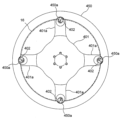
次に、上側乾燥モジュール205Aおよび下側乾燥モジュール205Bの構成について説明する。上側乾燥モジュール205Aおよび下側乾燥モジュール205Bは、いずれもロタゴニ乾燥を行う乾燥機である。上側乾燥モジュール205Aおよび下側乾燥モジュール205Bは同一の構成を有しているので、以下、上側乾燥モジュール205Aについて説明する。図14は、上側乾燥モジュール205Aを示す縦断面図であり、図15は上側乾燥モジュール205Aを示す平面図である。上側乾燥モジュール205Aは、基台401と、この基台401に支持された4本の円筒状の基板支持部材402とを備えている。基台401は回転軸406の上端に固定されており、この回転軸406は軸受405によって回転自在に支持されている。軸受405は回転軸406と平行に延びる円筒体407の内周面に固定されている。円筒体407の下端は架台409に取り付けられており、その位置は固定されている。回転軸406は、プーリ411,412およびベルト414を介してモータ415に連結されており、モータ415を駆動させることにより、基台401はその軸心を中心として回転するようになっている。
Next, the configurations of the
基台401の上面には回転カバー450が固定されている。なお、図14は回転カバー450の縦断面を示している。回転カバー450は半導体ウェハ16の全周を囲むように配置されている。回転カバー450の縦断面形状は径方向内側に傾斜している。また、回転カバー450の縦断面は滑らかな曲線から構成されている。回転カバー450の上端は半導体ウェハ16に近接しており、回転カバー450の上端の内径は、半導体ウェハ16の直径よりもやや大きく設定されている。また、回転カバー450の上端には、基板支持部材402の外周面形状に沿った切り欠き450aが各々の基板支持部材402に対応して形成されている。回転カバー450の底面には、斜めに延びる液体排出孔451が形成されている。
A
半導体ウェハ16の上方には、半導体ウェハ16の表面(フロント面)に洗浄液として純水を供給するフロントノズル454が配置されている。フロントノズル454は、半導体ウェハ16の中心を向いて配置されている。このフロントノズル454は、図示しない純水供給源(洗浄液供給源)に接続され、フロントノズル454を通じて半導体ウェハ16の表面の中心に純水が供給されるようになっている。洗浄液としては、純水以外に薬液が挙げられる。また、半導体ウェハ16の上方には、ロタゴニ乾燥を実行するための2つのノズル460,461が並列して配置されている。ノズル460は、半導体ウェハ16の表面にIPA蒸気(イソプロピルアルコールとN2ガスとの混合気)を供給するためのものであり、ノズル461は半導体ウェハ16の表面の乾燥を防ぐために純水を供給するものである。これらノズル460,461は半導体ウェハ16の径方向に沿って移動可能に構成されている。
A
回転軸406の内部には、洗浄液供給源465に接続されたバックノズル463と、乾燥気体供給源466に接続されたガスノズル464とが配置されている。洗浄液供給源465には、洗浄液として純水が貯留されており、バックノズル463を通じて半導体ウェハ16の裏面に純水が供給されるようになっている。また、乾燥気体供給源466には、乾燥気体として、N2ガスまたは乾燥空気などが貯留されており、ガスノズル464を通じて半導体ウェハ16の裏面に乾燥気体が供給されるようになっている。
Inside the
次に、フロントノズル454からの純水の供給を停止し、フロントノズル454を半導体ウェハ16から離れた所定の待機位置に移動させるとともに、2つのノズル460,461を半導体ウェハ16の上方の作業位置に移動させる。そして、半導体ウェハ16を30~150min-1の速度で低速回転させながら、ノズル460からIPA蒸気を、ノズル461から純水を半導体ウェハ16の表面に向かって供給する。このとき、半導体ウェハ16の裏面にもバックノズル463から純水を供給する。そして、2つのノズル460,461を同時に半導体ウェハ16の径方向に沿って移動させる。これにより、半導体ウェハ16の表面(上面)が乾燥される。
Next, the supply of pure water from the
その後、2つのノズル460,461を所定の待機位置に移動させ、バックノズル463からの純水の供給を停止する。そして、半導体ウェハ16を1000~1500min-1の速度で高速回転させ、半導体ウェハ16の裏面に付着している純水を振り落とす。このとき、ガスノズル464から乾燥気体を半導体ウェハ16の裏面に吹き付ける。このようにして半導体ウェハ16の裏面が乾燥される。乾燥された半導体ウェハ16は、図1に示す搬送ロボット22により乾燥モジュール205Aから取り出され、ウェハカセットに戻される。このようにして、研磨、洗浄、および乾燥を含む一連の処理が半導体ウェハに対して行われる。上述のように構成された乾燥モジュール205Aによれば、半導体ウェハ16の両面を迅速かつ効果的に乾燥することができ、また、正確に乾燥処理の終了時点を制御することができる。したがって、乾燥処理のための処理時間が洗浄プロセス全体の律速工程となることはない。また、洗浄部4に形成される上述した複数の洗浄ラインでの処理時間は平準化することができるので、プロセス全体のスループットを向上させることができる。
Thereafter, the two
本実施形態によれば、半導体ウェハを研磨装置に搬入した時(ロード前)に、半導体ウェハが乾燥状態にあり、研磨と洗浄が終了後、アンロード前に、半導体ウェハが乾燥状態になって、基板カセットにアンロードされる。乾燥状態の半導体ウェハを研磨装置からカセットに入れて、取り出すことが可能となる。すなわち、ドライイン/ドライアウトが可能である。 According to this embodiment, the semiconductor wafer is in a dry state when it is carried into the polishing apparatus (before loading), and after polishing and cleaning is completed and before unloading, the semiconductor wafer is in a dry state. , unloaded into the board cassette. It becomes possible to put a dry semiconductor wafer into a cassette and take it out from the polishing apparatus. That is, dry-in/dry-out is possible.
仮置き台180へ置かれた半導体ウェハは、第1搬送室191を介して第1洗浄室190又は第2洗浄室192へ搬送される。半導体ウェハは、第1洗浄室190又は第2洗浄室192において洗浄処理される。第1洗浄室190又は第2洗浄室192において洗浄処理された半導体ウェハは、第2搬送室193を介して乾燥室194へ搬送される。半導体ウェハは、乾燥室194において乾燥処理される。乾燥処理された半導体ウェハは、搬送ロボット22によって乾燥室194から取り出されてカセットへ戻される。
The semiconductor wafer placed on the temporary storage table 180 is transferred to the
図16は、本発明の一実施形態に係る研磨ユニット(研磨装置)の全体構成を示す概略図である。図16に示すように、研磨装置は、研磨テーブル30Aと、研磨対象物である半導体ウェハ等の基板を保持して研磨テーブル上の研磨面に押圧するトップリング31A(保持部)とを備えている。
FIG. 16 is a schematic diagram showing the overall configuration of a polishing unit (polishing apparatus) according to an embodiment of the present invention. As shown in FIG. 16, the polishing apparatus includes a polishing table 30A and a
第1研磨ユニット3Aは、研磨パッド10と、研磨パッド10に対向して配置される半導体ウェハ16との間で研磨を行うための研磨ユニットである。第1研磨ユニット3Aは、研磨パッド10を保持するための研磨テーブル30Aと、半導体ウェハ16を保持するためのトップリング31Aを有する。第1研磨ユニット3Aは、トップリング31Aを保持するための揺動アーム110と、揺動アーム110を揺動するための揺動軸モータ14(アーム駆動部)と、揺動軸モータ14に、駆動電力を供給するドライバ18を有する。さらに第1研磨ユニット3Aは、揺動アーム110に加わるアームトルクを検知するアームトルク検知部26と、アームトルク検知部26が検知したアームトルク26aに基づいて、研磨の終了を示す研磨終点を検出する終点検出部28とを有する。
The
図16~図29により説明する本実施形態によれば、複数の研磨ユニット(研磨装置)間で電流センサの計測結果の差が減少した研磨装置を提供することができる。本実施形態では、研磨終点検出手段として、アームトルクに基づく方法、研磨テーブルまたはトップリングを回転駆動する駆動部の駆動負荷を検出して利用する方法が可能である。本実施形態は、トップリングを揺動アームの端部に保持する方式において、アームトルクに基づいて研磨終点検出を行うことを説明するが、研磨テーブルまたはトップリングを回転駆動する駆動部の駆動負荷を検出して、研磨終点検出を行うことも同様に実施できる。 According to the present embodiment described with reference to FIGS. 16 to 29, it is possible to provide a polishing apparatus in which differences in measurement results of current sensors among a plurality of polishing units (polishing apparatuses) are reduced. In this embodiment, as the polishing end point detecting means, a method based on arm torque or a method of detecting and utilizing the drive load of a drive unit that rotationally drives the polishing table or top ring can be used. In this embodiment, the polishing end point is detected based on the arm torque in a method in which the top ring is held at the end of a swinging arm. It is also possible to detect the polishing end point by detecting the polishing end point.
保持部と揺動アームとアーム駆動部とトルク検知部は、組を構成し、同一の構成を有する組が、第1研磨ユニット3A、第2研磨ユニット3B、第3研磨ユニット3C、第4研磨ユニット3Dのそれぞれに設けられている。
The holding part, the swing arm, the arm drive part, and the torque detection part constitute a set, and the set having the same configuration is the
研磨テーブル30Aは、テーブル軸102を介してその下方に配置される駆動部であるモータ(図示せず)に連結されており、そのテーブル軸102周りに回転可能になっている。研磨テーブル30Aの上面には研磨パッド10が貼付されており、研磨パッド10の表面101が半導体ウェハ16を研磨する研磨面を構成している。研磨テーブル30Aの上方には研磨液供給ノズル(図示しない)が設置されており、研磨液供給ノズルによって研磨テーブル30A上の研磨パッド10に研磨液Qが供給される。図16に示すように、研磨テーブル30Aの内部には、半導体ウェハ16内に渦電流を生成して、当該渦電流を検出することにより研磨終点を検知できる渦電流センサ50が埋設されていてもよい。
The polishing table 30A is connected via a
トップリング31Aは、半導体ウェハ16を研磨面101に対して押圧するトップリング本体24と、半導体ウェハ16の外周縁を保持して半導体ウェハ16がトップリングから飛び出さないようにするリテーナリング23とから構成されている。
The
トップリング31Aは、トップリングシャフト111に接続されている。トップリングシャフト111は、図示しない上下動機構により揺動アーム110に対して上下動する。トップリングシャフト111の上下動により、揺動アーム110に対してトップリング31Aの全体を昇降させ位置決めする。
また、トップリングシャフト111はキー(図示せず)を介して回転筒112に連結されている。この回転筒112はその外周部にタイミングプーリ113を備えている。揺動アーム110にはトップリング用モータ114が固定されている。上記タイミングプーリ113は、タイミングベルト115を介してトップリング用モータ114に設けられたタイミングプーリ116に接続されている。トップリング用モータ114が回転すると、タイミングプーリ116、タイミングベルト115、およびタイミングプーリ113を介して回転筒112およびトップリングシャフト111が一体に回転し、トップリング31Aが回転する。
Furthermore, the
揺動アーム110は、揺動軸モータ14の回転軸に接続されている。揺動軸モータ14は揺動アームシャフト117に固定されている。従って、揺動アーム110は、揺動アームシャフト117に対して回転可能に支持されている。
The
トップリング31Aは、その下面に半導体ウェハ16などの基板を保持できる。揺動アーム110は、揺動アームシャフト117を中心として、旋回可能である。下面に半導体ウェハ16を保持したトップリング31Aは、揺動アーム110の旋回により、半導体ウェハ16の受取位置から研磨テーブル30Aの上方に移動される。そして、トップリング31Aを下降させて、半導体ウェハ16を研磨パッド10の表面(研磨面)101に押圧する。このとき、トップリング31Aおよび研磨テーブル30Aをそれぞれ回転させる。同時に、研磨テーブル30Aの上方に設けられた研磨液供給ノズルから研磨パッド10上に研磨液を供給する。このように、半導体ウェハ16を研磨パッド10の研磨面101に摺接させて、半導体ウェハ16の表面を研磨する。
The
第1研磨ユニット3Aは、研磨テーブル30Aを回転駆動するテーブル駆動部(図示しない)を有する。第1研磨ユニット3Aは、研磨テーブル30Aに加わるテーブルトルクを検知するテーブルトルク検知部(図示しない)を有してもよい。テーブルトルク検知部は、回転モータであるテーブル駆動部の電流からテーブルトルクを検知することができる。終点検出部28は、アームトルク検知部26が検知したアームトルク26aのみから研磨の終了を示す研磨終点を検出してもよいし、テーブルトルク検知部が検知したテーブルトルクも考慮して、研磨の終了を示す研磨終点を検出してもよい。
The
図16においては、揺動アーム110の、揺動軸モータ14への接続部において、アームトルク検知部26は、揺動アーム110に加わるアームトルク26aを検知する。具体的には、アーム駆動部は、揺動アーム110を回転させる揺動軸モータ(回転モータ)14であり、アームトルク検知部26は、揺動軸モータ14の電流値から、揺動アーム110に加わるアームトルク26aを検知する。揺動軸モータ14の電流値は、揺動アーム110の、揺動軸モータ14への接続部におけるアームトルクに依存する量である。揺動軸モータ14の電流値は、本実施形態では、ドライバ18から揺動軸モータ14に供給される電流値18b、または、ドライバ18内で生成される後述する電流指令18aである。
In FIG. 16, the arm
アームトルク検知部26によるアームトルク26aの検知方法を図17により説明する。ドライバ18は、制御部65から、揺動アーム110の位置に関する位置指令65aを入力される。位置指令65aは、揺動アームシャフト117に対する揺動アーム110の回転角度に相当するデータである。ドライバ18は、また、揺動軸モータ14に内蔵して取り付けられたエンコーダ36から、揺動アームシャフト117の回転角度36aを入力される。
A method for detecting
エンコーダ36は、揺動軸モータ14の回転軸の回転角度36a、すなわち揺動アームシャフト117の回転角度36aを検知することができるものである。図17では、揺動軸モータ14とエンコーダ36は、独立に図示されているが、実際は、揺動軸モータ14とエンコーダ36は、一体化している。このような一体型モータの一例として、フィードバックエンコーダ付き同期型ACサーボモータがある。
The
ドライバ18は、偏差回路38と、電流生成回路40と、PWM回路42とを有する。偏差回路38は、位置指令65aと回転角度36aから、位置指令65aと回転角度36aの偏差38aを求める。偏差38aと、電流値18bは、電流生成回路40に入力される。電流生成回路40は、偏差38aと、現在の電流値18bから、偏差38aに応じた電流指令18aを生成する。PWM回路42は、電流指令18aを入力されて、PWM(Pulse Width Modulation)制御により、電流値18bを生成する。電流値18bは、揺動軸モータ14を駆動できる3相(U相、V相、W相)の電流である。電流値18bは揺動軸モータ14に供給される。
The
電流指令18aは、揺動軸モータ14の電流値に依存する量であり、アームトルクに依存する量である。アームトルク検知部26は、電流指令18aに対して、AD変換、増幅、整流、実効値変換等の処理のうちの少なくとも1つの処理をしたのちに、終点検出部28に、アームトルク26aとして出力する。
The
電流値18bは、揺動軸モータ14の電流値そのものであるとともに、アームトルクに依存する量である。アームトルク検知部26は、電流値18bから、揺動アーム110に加わるアームトルクを検知してもよい。アームトルク検知部26は、電流値18bを検出する際に、ホールセンサ等の電流センサを用いることができる。
The
研磨テーブルを回転駆動するためのモータM3(第1の電動モータ、図2を参照)、トップリング31Aを回転駆動するためのモータM1(第2の電動モータ、図5を参照)、及び揺動アームを揺動するためのモータM2(第3の電動モータ、図5を参照)のうちの1つの電動モータの電流値を検出して、第1の出力を生成する電流検出部810によるモータ電流の検知方法を図17により説明する。本実施形態では、電流検出部810は、モータM2の電流値を検出して、第1の出力810aを生成する。電流検出部810には、3相(U相、V相、W相)の電流値18bが入力される。
A motor M3 (first electric motor, see FIG. 2) for rotationally driving the polishing table, a motor M1 (second electric motor, see FIG. 5) for rotationally driving the
電流検出部810は、U相、V相、W相の電流値18bのそれぞれの絶対値を算出した後に、これら3個の値を加算して第1の出力810aを生成する。電流検出部810は、生成された第1の出力810aを終点検出部28に出力する。なお、電流検出部810は、電動モータの3相の電流値の絶対値の2乗の和を第1の出力として生成してもよい。第1の出力は、トルクを示すことができる量であれば、任意の量とすることができる。例えば、電流検出部810は、制御部65が出力する位置指令65aを検出して、第1の出力810aを生成してもよい。制御部65が位置指令65aではなくて、速度指令を出力する場合は、電流検出部810は、制御部65が出力する速度指令を検出して、第1の出力810aを生成してもよい。モータM2の電流値18bを検出して、第1の出力810aを生成する場合と比較して、位置指令65aや速度指令を用いると以下の利点がある。ホールセンサ等の電流センサ等を用いて、電流値18bを検出する場合、電流センサと検出部とを接続する配線がノイズを拾う可能性がある。一方、制御部65の出力を直接利用する場合、配線が短いため、このようなノイズがほとんど発生しない。すなわちモータが発生させているトルクを、低ノイズ状態で検出可能であり、検出されたトルクを終点検出に使用することで、検出精度の改善が可能である。なお、電流検出部810は、偏差回路38が出力する偏差38aを検出して、第1の出力810aを生成してもよい。
After calculating the respective absolute values of the
第2の出力に基づいて、研磨の終了を示す研磨終点を検出する終点検出部28は、トップリング31Aにより半導体ウェハ16(被研磨物)に加わる面圧と、第1の出力810aとの対応関係を表す第1のデータを用いて、第1の出力810aから、第1の出力810aに対応する面圧を求める第1の処理部である。
An end
終点検出部28は、第1の処理部により得られる面圧と、第2の出力との対応関係を表す第2のデータを用いて、第1の処理部により得られる面圧に対応する第2の出力を求める第2の処理部でもある。本実施形態では、第1のデータは、トップリング31Aにより半導体ウェハ16に加わる面圧と、第1の出力810aとの対応関係を表す第1の関係式であり、第2のデータは、トップリング31Aにより半導体ウェハ16に加わる面圧と、第2の出力との対応関係を表す第2の関係式である。なお、第1のデータと第2のデータは、式であらわされるものに限らず、面圧と、第1の出力と第2の出力との対応関係を表形式で表すものでもよい。その他、対応関係を表すものであれば、任意の形式が可能である。
The end
本実施形態では、第1の関係式は、第1の出力を、面圧に関する2次の多項式で表す式であり、第2の関係式は、第2の出力を、面圧に関する2次の多項式で表す式である。第2のデータは、複数の、本実施形態では4台の研磨ユニットに対して共通なデータである。 In this embodiment, the first relational expression expresses the first output as a quadratic polynomial related to the surface pressure, and the second relational expression expresses the second output as a quadratic polynomial related to the surface pressure. This is an expression expressed as a polynomial. The second data is common data to a plurality of polishing units, four in this embodiment.
終点検出部28は、CPU,メモリ、入出力手段を有するコンピュータとして構成することができる。そのときは、半導体ウェハ16に加わる面圧と、第1の出力との対応関係を表す第1のデータを用いて、第1の出力から、第1の出力に対応する面圧を求める第1の処理手段、第1の処理部により得られる面圧と、第2の出力との対応関係を表す第2のデータを用いて、第1の処理部により得られる面圧に対応する第2の出力を求める第2の処理手段、として機能させるためのプログラムをメモリに格納することができる。
The end
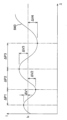
第1の関係式について以下説明し、さらに第1の関係式を求める方法についても、以下説明する。最初に、電流検出部810が検知した電流値18b、及びアームトルク検知部26が検知した電流指令18a(アームトルク)の具体的なデータの一例を図18以降に示す。研磨テーブル30Aのモータ電流のデータも示す。図18は、揺動軸モータ14のU相、V相、W相のうちの1つの相の電流値18bの絶対値を示す。図19は、研磨テーブル30Aのモータ電流U相、V相、W相のうちの1つの相の電流値の絶対値を示す。横軸は、研磨開始からの研磨時間(秒)であり、縦軸は電流(アンペア)である。面圧を変えながら電流値18bを検知した。研磨開始後、期間t1における面圧を、A psi(重量ポンド毎平方インチ)とすると、期間t2における面圧は、2倍の2A psiである。期間t3における面圧は、0 psi、すなわち、面圧を印可しない。
The first relational expression will be explained below, and a method for obtaining the first relational expression will also be explained below. First, examples of specific data of the
図18において、曲線812aは、1つの研磨ユニット812において、スラリを用いて研磨したものであり、曲線812bは、研磨ユニット812において、純水を用いて研磨したものである。曲線814aは、別の研磨ユニット814において、スラリを用いて研磨したものであり、曲線814bは、研磨ユニット814において、純水を用いて研磨したものである。
In FIG. 18, a
図19において、曲線812cは、研磨ユニット812において、スラリを用いて研磨したものであり、曲線812dは、研磨ユニット812において、純水を用いて研磨したものである。曲線814cは、別の研磨ユニット814において、スラリを用いて研磨したものであり、曲線814dは、研磨ユニット814において、純水を用いて研磨したものである。
In FIG. 19, a
図20、21は、それぞれ図18,19と同一のデータを、横軸を面圧、縦軸を電流として表わしたものである。ただし、電流に関しては、研磨開始後、期間t1の電流を平均して、面圧A psiに対する電流とし、期間t2の電流を平均して、面圧2A psiに対する電流とし、期間t2の電流を平均して、面圧0 psiに対する電流として、表示したものである。
20 and 21 show the same data as in FIGS. 18 and 19, respectively, with the horizontal axis representing surface pressure and the vertical axis representing current. However, regarding the current, after the start of polishing, the current for period t1 is averaged to be the current for the surface pressure A psi, the current for period t2 is averaged to be the current for the
図20において、曲線812eは、研磨ユニット812において、スラリを用いて研磨したものであり、曲線812fは、研磨ユニット812において、純水を用いて研磨したものである。曲線814eは、研磨ユニット814において、スラリを用いて研磨したものであり、曲線814fは、研磨ユニット814において、純水を用いて研磨したものである。
In FIG. 20, a
図21において、曲線812gは、研磨ユニット812において、スラリを用いて研磨したものであり、曲線812hは、研磨ユニット812において、純水を用いて研磨したものである。曲線814gは、別の研磨ユニット814において、スラリを用いて研磨したものであり、曲線814hは、研磨ユニット814において、純水を用いて研磨したものである。
In FIG. 21, a
図20、21より、アームトルク検知部26が検知した電流指令18aと、研磨テーブル30Aのモータ電流は、いずれも研磨ユニット間で絶対値が異なることがわかる。また、スラリを用いたときと、純水を用いたときで、電流値の絶対値は異なるが、面圧が増加すると電流値の絶対値が増加することがわかる。研磨ユニットが異なっても、面圧が増加すると電流値の絶対値が増加することがわかる。研磨ユニット間で絶対値が異なるため、しきい値やマージンの設定が研磨ユニット毎に異なるため、設定が煩雑であり、設定に時間を要する。補正により電流値、すなわち出力の研磨ユニット間の差を無くす必要がある。
20 and 21, it can be seen that the
出力の研磨ユニット間の差が生じる原因を分析するために、揺動軸モータ14に関して、電流検出部810が検出したU、V、W相出力と、アームトルク検知部26が検出した電流指令18aを確認した。図22、23は、電流検出部810が検出したU、V、W相出力の1例を示す。図22は、1つの研磨ユニット820に関する電流値であり、図23は、別の研磨ユニット822に関する電流値である。図22、23において、横軸は、研磨開始からの研磨時間(秒)であり、縦軸は電流(アンペア)である。面圧を変えながら電流値18bを検知した。期間t1の面圧は、A psi、期間t2の面圧は、2A psiである。期間t3の面圧は、0 psiである。
In order to analyze the cause of the difference in output between the polishing units, the U, V, and W phase outputs detected by the
図22と、図23とを比較すると、研磨ユニット820と研磨ユニット822では、U、V、W相の極性が異なっていた。従って、U、V、W相のうちの1相、例えばV相のみの計測では、研磨ユニット間で絶対値が大きく異なる場合があることがわかる。 Comparing FIG. 22 and FIG. 23, the polarities of the U, V, and W phases were different in the polishing unit 820 and the polishing unit 822. Therefore, it can be seen that when measuring only one phase among the U, V, and W phases, for example, the V phase, the absolute value may differ greatly between polishing units.
図24、25は、アームトルク検知部26が検出した電流指令18aを示す。図24は、研磨ユニット820に関する電流値であり、図25は、研磨ユニット822に関する電流値である。図24、25において、横軸は、研磨開始からの研磨時間(秒)であり、縦軸は電流(アンペア)である。面圧を変えながら電流指令18aを検知した。期間t1の面圧は、A psi、期間t2の面圧は、2A psiである。期間t3の面圧は、0 psiである。図24と、図25とを比較すると、研磨ユニット812と研磨ユニット814では、電流指令18aは、ほぼ同等であることがわかる。
24 and 25 show the
図26に、電流検出部810に入力されるU、V、W相出力の絶対値を取った後に足し合わせた結果の1例を示す。図26は、図22、23に示すデータを用いて作成したものである。曲線820aは、研磨ユニット820、曲線822aは、研磨ユニット822に関して得られたデータである。横軸は、研磨開始からの研磨時間(秒)であり、縦軸は電流(アンペア)である。期間t1の面圧は、A psi、期間t2の面圧は、2A psiである。期間t3の面圧は、0 psiである。
FIG. 26 shows an example of the result obtained by taking the absolute values of the U, V, and W phase outputs input to the
図26より、研磨ユニット間で、面圧の変化により電流出力は異なるが、図22,23に示すV相のように、研磨ユニット間で大きく異なることはない。このため、補正を行うことで、研磨ユニット間で同等にできると考えられる。図25,26から、研磨ユニット間のセンサの出力差を減らすための手法として、(1)トルク指令値を計測すること、または(2)U、V、W相の電流を合成することが好ましいと考えられる。 From FIG. 26, although the current output differs between polishing units due to changes in surface pressure, there is no large difference between polishing units as in the V phase shown in FIGS. 22 and 23. Therefore, it is thought that by making corrections, the polishing units can be made equivalent. From Figures 25 and 26, it is preferable to (1) measure the torque command value or (2) synthesize the U, V, and W phase currents as a method to reduce the sensor output difference between polishing units. it is conceivable that.
次に、U、V、W相の電流を合成して、センサ出力とする場合について、第1の関係式について説明する。第1の関係式をy=f(x)とすると、y(第1の出力)は、U、V、W相の電流を合成して得られるセンサ出力である。xは、面圧である。f(x)が、xに関するN次近似式、すなわち、
y=f(x)=kN*xn+(kN-1)*xN-1+(kN-2)*xN-2+・・・k2*x2+k1*x+k0
(ここで、kN,kN-1,kN-2,・・・,k2,k1,k0は、定数である。)
である場合、以下のようにして、kN,kN-1,kN-2,・・・,k2,k1,k0を求める。
(1) 研磨ユニット毎に、基準となる半導体ウェハ16に関して、面圧に対するU、V、W相の電流を検出して、絶対値の和を求める。これをN+1個以上の異なる面圧について求める。
(2) (1)で得られた結果から研磨ユニット毎に、上記のN次近似式を算出する。N+1個の異なる面圧に関する測定値が得られる場合は、連立1次方程式を解くことにより、kN,kN-1,kN-2,・・・,k2,k1,k0を求める。N+2個以上の異なる面圧に関する測定値が得られる場合は、回帰分析を行うことにより、kN,kN-1,kN-2,・・・,k2,k1,k0を求める。
Next, the first relational expression will be described in the case where the U, V, and W phase currents are combined and used as a sensor output. When the first relational expression is y=f(x), y (first output) is a sensor output obtained by combining U, V, and W phase currents. x is surface pressure. f(x) is an N-th approximation formula for x, that is,
y=f(x)=kN*x n +(kN-1)*x N-1 +(kN-2)*x N-2 +...k2*x 2 +k1*x+k0
(Here, kN, kN-1, kN-2,..., k2, k1, k0 are constants.)
If so, kN, kN-1, kN-2, . . . , k2, k1, k0 are determined as follows.
(1) For each polishing unit, detect the U, V, and W phase currents with respect to the surface pressure with respect to the
(2) Calculate the above Nth-order approximation formula for each polishing unit from the results obtained in (1). When measurement values related to N+1 different surface pressures are obtained, kN, kN-1, kN-2, . . . , k2, k1, k0 are determined by solving simultaneous linear equations. If measurement values related to N+2 or more different surface pressures are obtained, kN, kN-1, kN-2, . . . , k2, k1, k0 are determined by regression analysis.
(3)第2の関係式をy=g(x)とすると、y(第2の出力)は、補正後のセンサ出力である。xは、面圧である。g(x)が、xに関するM次近似式、すなわち、
y=g(x)=lM*xM+(lM-1)*xM-1+(lM-2)*xM-2+・・・+l2*x2+l1*x+l0
(ここで、lM,lM-1,lM-2,・・・,l2,l1,l0は、定数である。)
である場合、以下のようにして、lM,lM-1,lM-2,・・・,l2,l1,l0を求める。なお、NとMは、異なってもよいが、同じであることが好ましい。以下では、NとMは、同じであるとする。
(3) If the second relational expression is y=g(x), y (second output) is the corrected sensor output. x is surface pressure. g(x) is an M-th approximation formula for x, that is,
y=g(x)=lM*x M +(lM-1)*x M-1 +(lM-2)*x M-2 +...+l2*x2+l1*x+l0
(Here, lM, lM-1, lM-2,..., l2, l1, l0 are constants.)
If , lM, lM-1, lM-2, . . . , l2, l1, l0 are determined as follows. Note that N and M may be different, but are preferably the same. In the following, it is assumed that N and M are the same.
第1の関係式y=f(x)は、上述のように研磨ユニット毎に求められる。研磨ユニットが、例えば4台あるとする。このとき、4個の第1の関係式y=f(x)が得られる。これらを、y=f1(x)、y=f2(x)、y=f3(x)、y=f4(x)とする。第2の関係式y=g(x)は、例えば、4個の第1の関係式f1(x)、y=f2(x)、y=f3(x)、y=f4(x)のうちの1つとすることができる。すなわち、g(x)=f3(x)とすることができる。 The first relational expression y=f(x) is determined for each polishing unit as described above. Assume that there are, for example, four polishing units. At this time, four first relational expressions y=f(x) are obtained. Let these be y=f1(x), y=f2(x), y=f3(x), and y=f4(x). The second relational expression y=g(x) is, for example, one of the four first relational expressions f1(x), y=f2(x), y=f3(x), and y=f4(x). It can be one of the following. That is, it can be set as g(x)=f3(x).
別の方法として、第2の関係式y=g(x)は、4個の第1の関係式y=f1(x)、y=f2(x)、y=f3(x)、y=f4(x)の平均とすることができる。すなわち、g(x)=(f1(x)+f2(x)+f3(x)+f4(x))/4 とすることができる。第1の関係式y=f(x)と、第2の関係式y=g(x)は、研磨ユニットで、例えば新たなプロセスで作成された半導体ウェハ16の研磨を開始するときに、上記のようにして、測定して算出することができる。また、センサまたは研磨テーブル等が改良されたとき等に、第1の関係式y=f(x)と、第2の関係式y=g(x)を、上記のようにして、測定して算出することができる。
Alternatively, the second relation y=g(x) can be combined with the four first relations y=f1(x), y=f2(x), y=f3(x), y=f4 (x). That is, g(x)=(f1(x)+f2(x)+f3(x)+f4(x))/4. The first relational expression y=f(x) and the second relational expression y=g(x) are used when the polishing unit starts polishing the
第1の関係式y=f(x)と、第2の関係式y=g(x)が得られた後に、第1の処理部が、半導体ウェハ16に加わる面圧と、第1の出力との対応関係を表す第1の関係式y=f(x)を用いて、第1の出力から、第1の出力に対応する面圧を求める方法について、次に説明する。研摩中に、U、V、W相の電流を検知する。これらを合成して、例えば、絶対値の和を求めることにより、現在のセンサ値が得られる。これは、第1の関係式y=f(x)におけるyに相当する量である。各研磨ユニットにおいて、研磨ユニット毎の第1の関係式y=f(x)から逆算して面圧xを求める。すなわち、N次方程式を解くことにより、研磨ユニット毎に面圧xを求めることができる。
After obtaining the first relational expression y=f(x) and the second relational expression y=g(x), the first processing section calculates the surface pressure applied to the
次に、第2の処理部が、第1の処理部により得られる面圧と、第2の出力との対応関係を表す第2の関係式を用いて、第1の処理部により得られる面圧に対応する第2の出力を求める方法について、次に説明する。研摩中に、研磨ユニット毎に面圧xが求まると、第2の処理部は、すべての研磨ユニットに対して共通な第2の関係式y=g(x)のxに、得られた面圧を代入して、第2の出力を求める。こうして、補正後のセンサ出力を得る。 Next, the second processing section uses a second relational expression representing the correspondence between the surface pressure obtained by the first processing section and the second output to determine the surface obtained by the first processing section. A method for determining the second output corresponding to the pressure will be described next. During polishing, when the surface pressure x is determined for each polishing unit, the second processing section applies the obtained surface pressure to x in the second relational expression y=g(x) that is common to all polishing units. Substitute the pressure to find the second output. In this way, a corrected sensor output is obtained.
N次近似式を用いた場合を説明したが、次に、N=2の場合について説明する。最初に、第1の関係式の作成方法について説明する。
(1)4台の研磨ユニット毎に、基準となる半導体ウェハ16に関して、面圧に対するU、V、W相の電流を検出して、絶対値の和を求める。これを3個の異なる面圧について求める。一例として、面圧p1、p2、p3に対して、センサ値がs1、s2、s3として得られたとする。
(2) (1)で得られた結果から研磨ユニット毎に、下記の2次近似式を算出する。3個の異なる面圧p1、p2、p3に関するセンサ値s1、s2、s3を下記の式に代入して、連立1次方程式を解くことにより、2次式の係数ac,bc,ccを求める。
yc=acx2+bcx+cc ここで、x:面圧, y:センサ値
4台の研磨ユニット毎に、1つの式が得られ、合計で4個の2次近似式が算出される。4個の2次近似式を図27に示す。図27において横軸は、x:面圧であり、縦軸は、y:センサ値である。4本の曲線824a~曲線824d(第1の関係式)が得られる。
The case where the N-th approximation formula is used has been described, but next, the case where N=2 will be described. First, a method for creating the first relational expression will be explained.
(1) For each of the four polishing units, detect the U, V, and W phase currents with respect to the surface pressure with respect to the
(2) From the results obtained in (1), calculate the following quadratic approximation formula for each polishing unit. By substituting the sensor values s1, s2, and s3 regarding three different surface pressures p1, p2, and p3 into the equation below and solving the simultaneous linear equations, the coefficients a c , b c , c c of the quadratic equation are calculated. seek.
y c = a c x 2 + b c x + c c where x: surface pressure, y: sensor value One formula is obtained for each of the four polishing units, and a total of four quadratic approximation formulas are calculated. Ru. FIG. 27 shows four quadratic approximations. In FIG. 27, the horizontal axis is x: surface pressure, and the vertical axis is y: sensor value. Four
(3)次に、第2の関係式をy=g(x)とすると、y(第2の出力)は、補正後のセンサ出力である。xは、面圧である。g(x)として、例えば、4台の研磨ユニットとは別の研磨ユニットに関して既に得られている2次近似式を選択することができる。選択した結果を
g(x)=yr=arx2+brx+cr とする。選択した第2の関係式を図28に曲線826として示す。図28において横軸は、x:面圧であり、縦軸は、y:センサ値である。このようにして、第1の関係式y=f(x)と、第2の関係式y=g(x)が得られる。
(3) Next, when the second relational expression is y=g(x), y (second output) is the corrected sensor output. x is surface pressure. As g(x), for example, a quadratic approximation formula that has already been obtained for a polishing unit other than the four polishing units can be selected. Let the selected result be g(x)=y r =a r x 2 +br x +c r . The selected second relational expression is shown as
図27に示す第1の関係式と、図28に示す第2の関係式とを、4台の研磨ユニット毎に、図29に示す。図29a~図29dは、4台の研磨ユニット毎に第1の関係式と第2の関係式を示す。図29において横軸は、x:面圧であり、縦軸は、y:センサ値である。 The first relational expression shown in FIG. 27 and the second relational expression shown in FIG. 28 are shown in FIG. 29 for each of the four polishing units. 29a to 29d show the first relational expression and the second relational expression for each of the four polishing units. In FIG. 29, the horizontal axis is x: surface pressure, and the vertical axis is y: sensor value.
次に、第1の関係式y=f(x)と、第2の関係式y=g(x)を用いて、第1の処理部と第2の処理部は、次のような処理を行う。 Next, using the first relational expression y=f(x) and the second relational expression y=g(x), the first processing section and the second processing section perform the following processing. conduct.
研摩中に、U、V、W相の電流を検知する。これらを合成して、例えば、絶対値の和を求めることにより、現在のセンサ値が得られる。これは、第1の関係式yc=acx2+bcx+ccにおけるyに相当する量である。第1の処理部は、研磨ユニット毎の第1の関係式y=f(x)から逆算して、各ユニット毎に面圧xを求める。すなわち、2次方程式を解くことにより、すなわち、2次方程式の根の公式から、以下のように、研磨ユニット毎に面圧xを求めることができる。
x=(-bc+sqrt(bc
2-4ac(cc-yc))/2ac
During polishing, U, V, and W phase currents are detected. The current sensor value can be obtained by combining these and finding the sum of absolute values, for example. This is the amount equivalent to y in the first relational expression y c =ac x 2 +b c x+c c . The first processing section calculates back from the first relational expression y=f(x) for each polishing unit to obtain the surface pressure x for each unit. That is, by solving the quadratic equation, that is, from the root formula of the quadratic equation, the surface pressure x can be determined for each polishing unit as follows.
x=(-b c +sqrt(b c 2 -4a c (c c -y c ))/2a c
研摩中に、第1の処理部により研磨ユニット毎に面圧xが求まると、第2の処理部は、すべての研磨ユニットに対して共通な第2の関係式y=arx2+brx+cr のxに、得られた面圧を代入して、第2の出力を研磨ユニット毎に求める。こうして、補正後のセンサ出力を研磨ユニット毎に得る。 During polishing, when the first processing section determines the surface pressure x for each polishing unit, the second processing section calculates the second relational expression y=a r x 2 + b r that is common to all polishing units. The obtained surface pressure is substituted for x in x+ cr to obtain the second output for each polishing unit. In this way, a corrected sensor output is obtained for each polishing unit.
本実施形態では、以上のように、第2の関係式は、複数の研磨ユニット間で同一のものとすることができる。第2の関係式を用いて、第1の処理部により得られる面圧に対応する第2の出力を求めるため、同一の面圧に対しては、複数の研磨ユニット間で、同一の第2の出力を得ることができる。従って、複数の研磨ユニット間で電流センサの計測結果の差が減少した研磨ユニットを提供することができる。研磨ユニットが100台を超える場合があり、これらに対して、共通の設定値で済むということは、運転コストの低減に効果がある。 In this embodiment, as described above, the second relational expression can be made the same among a plurality of polishing units. In order to obtain the second output corresponding to the surface pressure obtained by the first processing section using the second relational expression, for the same surface pressure, the same second output You can get the output of Therefore, it is possible to provide a polishing unit in which the difference in the measurement results of the current sensor among the plurality of polishing units is reduced. There are cases where there are more than 100 polishing units, and the fact that common setting values are sufficient for these units is effective in reducing operating costs.
本実施形態では、第1の関係式は、研磨条件が変わったとき等に作成し直す。すなわち、研磨テーブル30A、研磨パッド10(摩耗して、同じ仕様のパッドに交換した時は再作成しない)、センサ、半導体ウェハ16(製造プロセスが異なる半導体ウェハ16になった時)が変わったときに、第1の関係式は再作成する。
In this embodiment, the first relational expression is re-created when the polishing conditions change. That is, when the polishing table 30A, the polishing pad 10 (do not recreate it when it wears out and is replaced with a pad of the same specifications), the sensor, and the semiconductor wafer 16 (when the
第1の関係式は、純水を用いて研磨して得られる測定値を用いて作成することが好ましい。スラリを用いると、スラリの成分や供給量の少しの変化によって、センサ出力が大きく変わる場合があるからである。すなわち、純水を用いて研磨する場合は、研磨状態を再現することが容易である。このため、純水を用いて研磨して得られる測定値を用いて作成した場合、純水を流して研磨することにより、モータや研磨装置の異常を検出しやすい。純水は、スラリと異なり、常に一定の条件の純水を再現性良く容易に得ることができるため、モータや研磨装置の各部の異常のみを、事前に得られた第2の関係式の出力と比較することにより、容易に検出できるからである。異常検出のため、定期的に、純水での研磨を行うことが好ましい。 The first relational expression is preferably created using measured values obtained by polishing using pure water. This is because when a slurry is used, the sensor output may change significantly due to a slight change in the slurry components or supply amount. That is, when polishing is performed using pure water, it is easy to reproduce the polishing state. For this reason, when a measurement value obtained by polishing using pure water is used to create a measurement value, abnormalities in the motor or polishing device can be easily detected by polishing by flowing pure water. Unlike slurry, pure water can always be easily obtained under constant conditions with good reproducibility, so only abnormalities in the motor and polishing equipment can be detected using the output of the second relational expression obtained in advance. This is because it can be easily detected by comparing with. In order to detect abnormalities, it is preferable to periodically perform polishing with pure water.
なお、第1の関係式と第2の関係式は、面圧を自動的に変えることにより、自動的に作成することができる。 Note that the first relational expression and the second relational expression can be automatically created by automatically changing the surface pressure.
第1の関係式及び第2の関係式おいて、yが3相の電流値である場合について説明したが、yはトルク指令値でもよい。3相の電流値は、トルク指令値と比較するとモータに、より近い部分に位置するため、摩擦力の変化に敏感、又は忠実であると考えられる。 In the first relational expression and the second relational expression, a case has been described in which y is a three-phase current value, but y may be a torque command value. Since the three-phase current values are located closer to the motor than the torque command values, they are considered to be sensitive to or faithful to changes in frictional force.
揺動アーム110が静止しているときの駆動モータの電流センサに、本実施形態を適用することが好ましい。揺動アーム110や研磨テーブル30Aが回転しているときは、揺動アーム110や研磨テーブル30Aの付属品やベアリングの影響を受けるために、モータの駆動電流には、多くのノイズが発生するためである。揺動アーム110や研磨テーブル30Aが回転しているときにも、ノイズを低減することにより、本発明は適用できる。
It is preferable to apply this embodiment to the current sensor of the drive motor when the
本実施形態では、純水を用いて標準的な半導体ウェハ16(又は実際に研磨対象とする半導体ウェハ16)を研磨することにより第1の関係式を求め、実際の研磨で、スラリを使用した場合でも、本方法は有効である理由は以下のとおりである。電流式センサの出力は、半導体ウェハ16と研磨パッド10との間に生じる摩擦力に依存する。摩擦力は主に、面圧と、半導体ウェハ16と研磨パッド10との間の摩擦係数と、回転速度に依存する。
In this embodiment, the first relational expression is obtained by polishing a standard semiconductor wafer 16 (or the
第1の関係式を求めたときの摩擦係数は、純水であり、実際の研磨は、スラリで行うため、摩擦係数は異なる。面圧や回転速度が同じであっても、純水であるかスラリであるかにより、摩擦力は異なる。すなわち、同じ面圧や回転速度を付加した時のセンサ出力は、純水とスラリでは、図18,19等に示すように異なる。しかし、第1の関係式を利用した本実施形態の既述の方法は有効と考えられる。 The friction coefficient when calculating the first relational expression is pure water, and since actual polishing is performed using slurry, the friction coefficient is different. Even if the surface pressure and rotational speed are the same, the frictional force will differ depending on whether it is pure water or slurry. That is, when the same surface pressure and rotational speed are applied, the sensor output differs between pure water and slurry, as shown in FIGS. 18 and 19. However, the method described above in this embodiment using the first relational expression is considered to be effective.
なぜならば本方法によれば、図20,21に示すように、スラリを用いた場合、研磨ユニットによらず、ほぼ同じ大きさで、同じ増加傾向を示すセンサ出力を得ることができるからである。研磨の進行に伴い、摩擦係数のみが変化する場合(すなわち、半導体ウェハ16の表面状態のみが変化する場合)、電流センサの出力の変化の仕方は、研磨ユニットによらず、同じ傾向を示す。従って、電流センサの出力の変化を検知して研磨終了時点を検出するという目的は達成できる。
This is because according to this method, as shown in FIGS. 20 and 21, when slurry is used, it is possible to obtain sensor outputs of approximately the same size and showing the same increasing tendency, regardless of the polishing unit. . When only the friction coefficient changes as the polishing progresses (that is, when only the surface condition of the
次に、図30により、光学式センサを有する別の実施形態を説明する。本形態では、研磨テーブル30Aを揺動する揺動軸モータ14のトルク変動の検知と、光学式センサによる半導体ウェハ16の研磨面の反射率の検知を併用する。終点検知のために、研磨テーブル30Aにセンサが組み込まれている。センサは光学式センサ724である。光学式センサ724としては、ファイバを利用したセンサ等が使用される。なお、光学式センサ724の代わりに、渦電流センサを用いることもできる。
Next, another embodiment having an optical sensor will be described with reference to FIG. In this embodiment, detection of the torque fluctuation of the
図30の実施形態の場合、以下の課題を解決することができる。終点検知のために、トルク変動検知方式又は光学式検知方式の一方のみを用いた場合、研磨対象物の研磨に、金属膜の研磨と絶縁膜の研磨が混在する場合、以下の問題がある。トルク変動検知方式は、金属膜と絶縁膜の境界の検知に適しており、光学式検知方式は、膜の厚さの変化の検知に適している。そのため、一方の方式のみでは、膜の境界の検知と、残膜の厚さの検知の両方が必要な場合に、不十分な検知精度しか得られない。膜の境界の検知と、残膜の厚さの検知のいずれであるかに応じて、トルク変動検知と光学式検知を使い分けることにより、課題が解決できる。 In the case of the embodiment shown in FIG. 30, the following problems can be solved. When only one of the torque fluctuation detection method or the optical detection method is used to detect the end point, the following problems occur when the polishing of the object to be polished involves both polishing of a metal film and polishing of an insulating film. The torque fluctuation detection method is suitable for detecting the boundary between a metal film and an insulating film, and the optical detection method is suitable for detecting changes in film thickness. Therefore, if only one method is used, insufficient detection accuracy can be obtained when both the film boundary detection and the residual film thickness detection are required. The problem can be solved by selectively using torque fluctuation detection and optical detection depending on whether the detection is the boundary of the film or the thickness of the remaining film.
光学式センサの場合、研磨装置の終点検出部は、半導体ウェハ16に光を当て、半導体ウェハ16からの反射光の強度を計測する。終点検出部は、アームトルク検知部が検知したアームトルクと、光学式センサ724が計測した半導体ウェハ16からの反射光の強度とに基づいて、研磨の終了を示す研磨終点を検出する。光学式センサ724の出力は、配線726を介して、制御部65に送られる。
In the case of an optical sensor, the end point detection section of the polishing apparatus illuminates the
光学式センサの場合、研磨パッド10の一部に開口720がある。開口720に、ウィンドウであるビューポート722がある。ビューポート722を介して、光照射と、反射光の検知が行われる。研磨時に半導体ウェハ16と対向可能な、研磨テーブル30A内の位置にビューポート722は組込まれる。ビューポート722の下部に、光学式センサ724が配置される。光学式センサ724がファイバセンサの場合は、ビューポート722が無い場合もある。
In the case of an optical sensor, there is an
ビューポート722が無い場合、ファイバセンサの周囲から純水を出して、ノズル728から供給されるスラリを除去して終点検知を行う場合もある。光学式センサは、スラリを洗浄するための純水(又は高純度ガス、液体とガスの混合物などの流体)を開口420内に供給する流体供給部(図示しない)を有する。
If there is no
センサは複数あってもよい。例えば、図30に示すように、中心部と端部に設けて、中心部と端部の双方における検知信号をモニタする。図30(a)は、光学式センサ724の配置を示し、図30(b)は、光学式センサ724の拡大図である。終点検出部28は、それらの複数の信号の中から、研磨条件(半導体ウェハ16の材質、研磨時間等)の変化に応じて、研磨条件の影響を受けない(もしくは、当該研磨条件に最適な)検知信号を選んで、終点を判断して、研磨を止める。
There may be multiple sensors. For example, as shown in FIG. 30, they are provided at the center and at the ends to monitor detection signals at both the center and the ends. 30(a) shows the arrangement of the
この点について、さらに説明する。既述の揺動軸モータ14によるトルク変動検知(モータ電流変動測定)と、光学式検知の組合せは、層間絶縁膜(ILD)や、STI(Shallow Trench Isolation)による素子分離膜の研磨終点を検知することに用いると、有効である。SOPM(Spectrum Optical Endpoint Monitoring)等の光学式検知では、残膜の厚さの検出を行い、終点検知を行う。例えば、LSIの積層膜の製造プロセスにおいて、金属膜の研磨と絶縁膜の研磨により、残膜を形成することが必要な場合がある。金属膜の研磨と絶縁膜の研磨を行う必要があり、金属膜の研磨と絶縁膜の研磨のいずれであるかに応じて、トルク変動検知と光学式検知を使い分けることが可能となる。
This point will be further explained. The combination of torque fluctuation detection (motor current fluctuation measurement) by the aforementioned
また、終点部の膜構造が金属と絶縁膜の混在状態である場合、トルク変動検知と光学式検知のうちの一方式だけでは、正確な終点検知が困難である。そのため、トルク変動検知と光学式検知による膜厚測定を行い、双方の検知結果より、終点であるかを判定して、最適な時点で研磨を終了する。混在状態では、トルク変動検知と光学式検知のいずれにおいても測定信号が弱いために測定精度が低下する。しかし、2種類以上の測定方法により得られた信号を用いて判定することにより、最適な終点位置を判定することが可能となる。例えば、2種類以上の測定方法により得られた信号を用いた判定のいずれもが、終点であるという結果を出した時に終点であると判断する。 Furthermore, if the film structure at the end point is a mixture of metal and insulating film, it is difficult to accurately detect the end point using only one of torque fluctuation detection and optical detection. Therefore, the film thickness is measured by torque fluctuation detection and optical detection, and based on the detection results of both, it is determined whether the end point has been reached and the polishing is finished at the optimal point. In a mixed state, measurement accuracy decreases because the measurement signal is weak in both torque fluctuation detection and optical detection. However, by making a determination using signals obtained by two or more types of measurement methods, it becomes possible to determine the optimal end point position. For example, it is determined that the end point has been reached when all of the determinations using signals obtained by two or more types of measurement methods have resulted in the end point.
次に、図31により、光学式センサを有する別の実施形態を説明する。本形態では、研磨テーブル30Aを揺動する揺動軸モータ14のトルク変動(研磨テーブル30Aの摩擦変動)の検知と、光学式センサによる半導体ウェハ16の研磨面の反射率の検知と、渦電流センサによる半導体ウェハ16の被研磨物内の渦電流の検知を併用する。3種類の検知方法が併用される。
Next, another embodiment having an optical sensor will be described with reference to FIG. 31. In this embodiment, detection of the torque fluctuation of the
図31の実施形態の場合、以下の課題を解決することができる。図30の実施形態のトルク変動検知方式および光学式検知方式は、金属膜の厚さの変化を検知することが難しいという課題がある。図31の実施形態は、この課題を解決するものであり、図30の実施形態に、さらに、渦電流の検知を併用している。金属膜内の渦電流を検知するため、金属膜の厚さの変化を検知することが、より容易になる。 In the case of the embodiment shown in FIG. 31, the following problems can be solved. The torque fluctuation detection method and optical detection method of the embodiment shown in FIG. 30 have a problem in that it is difficult to detect changes in the thickness of the metal film. The embodiment of FIG. 31 solves this problem, and further uses eddy current detection in addition to the embodiment of FIG. 30. Because the eddy currents within the metal film are detected, it becomes easier to detect changes in the thickness of the metal film.
図31(a)は、光学式センサ724と、渦電流式センサ730の配置を示し、図31(b)は、光学式センサ724の拡大図であり、図31(c)は、渦電流式センサ730の拡大図である。渦電流式センサ730は、研磨テーブル30A内に配置される。渦電流式センサ730は、半導体ウェハ16に磁場を生成し、生成した磁場の強度を検知する。終点検出部28は、アームトルク検知部26が検知したアームトルクと、光学式センサ724が計測した半導体ウェハ16からの反射光の強度と、渦電流式センサ730が計測した磁場の強度とに基づいて、研磨の終了を示す研磨終点を検出する。
31(a) shows the arrangement of the
本形態は、終点検知のために、揺動軸モータ14のトルク変動検出、研磨テーブル30Aに組み込まれた光学式センサ724と渦電流式センサ730による半導体ウェハ16の物理量の検出とが組み合わされた例である。揺動軸モータ14のトルク変動検知(モータ電流変動測定)は、研磨する試料の膜質が変化する部位の終点検知に優れる。光学方式は、ILD、STIなどの絶縁膜の残膜量の検出と、それによる終点検出に優れる。渦電流センサによる終点検出は、例えばめっきされた金属膜を研磨して終点である下層の絶縁膜まで研磨した時点の終点検出に優れる。
In this embodiment, in order to detect the end point, detection of the torque fluctuation of the
LSIなどの多層を有する半導体の製造プロセスにおいては、種々の材料からなる多層の研磨を行うことになるので、多様な膜の研磨と終点検出を高精度にて行うため、一実施態様においては3種類の終点検出方法を用いることができ、3種類以上も可能である。例えば、さらに、研磨テーブル30Aを回転させるモータのトルク変動検知(モータ電流変動測定(TCM))を併用することができる。 In the manufacturing process of semiconductors with multiple layers such as LSI, multiple layers made of various materials are polished. Therefore, in order to polish various films and detect the end point with high precision, in one embodiment, three Various types of end point detection methods can be used, and three or more types are possible. For example, detection of torque fluctuations in the motor that rotates the polishing table 30A (motor current fluctuation measurement (TCM)) can also be used.
これら4種類の終点検出の組合せを用いて、高機能な制御や精度のよい終点検知を行うことが可能となる。例えば、研磨テーブル30A上をトップリング31Aが移動して(揺動して)研磨を行っている場合、トップリング31Aの位置の変化による研磨テーブル30Aのトルク変動をTCMにより検出する。これにより、トップリング31Aが研磨テーブル30Aの中心部にある時、トップリング31Aが研磨テーブル30Aの一方の端部に移動した時、トップリング31Aが研磨テーブル30Aの他方の端部に移動した時のトルク変動により、トップリング31Aの試料への押圧が異なる要因を見つけることが可能となる。要因が見つかると、試料への押圧を均一化するために、トップリング31Aの表面の押圧の調整を行う等のフィードバックを行うことができる。
By using a combination of these four types of end point detection, it becomes possible to perform highly functional control and accurate end point detection. For example, when the
トップリング31Aの位置の変化による研磨テーブル30Aのトルク変動の要因としては、トップリング31Aと研磨テーブル30Aの水平度のズレや、試料面と研磨パッド10の表面の水平度のズレ、又は、研磨パッド10の摩耗度の差異により、中心部にトップリング31Aがある時と、中心部からずれた位置にトップリング31Aがある時の摩擦力が異なる等が考えられる。
Factors that cause torque fluctuations on the polishing table 30A due to changes in the position of the
なお、半導体ウェハ16の膜の研磨終点部の膜構造が金属と絶縁膜の混在状態である場合、1つの検知方式だけでは正確な終点検知が困難であるため、アームトルク変動を検知する方式と光学式検知方法、あるいは、アームトルク変動を検知する方式と渦電流を検知する方式、あるいは、3種類全ての信号検出から終点状態を判定して、最適な時点で研磨を終了する。混在状態では、トルク変動検知と光学式と検知渦電流を検知する方式のいずれにおいても測定信号が弱いために測定精度が低下する。しかし、3種類以上の測定方法により得られた信号を用いて判定することにより、最適な終点位置を判定することが可能となる。例えば、3種類以上の測定方法により得られた信号を用いた判定のいずれもが、終点であるという結果を出した時に終点であると判断する。
Note that if the film structure at the polishing end point of the
これらの組み合わせを列記すると、以下のとおりである。
i.アームトルク検知+テーブルトルク検知
ii.アームトルク検知+光学式検知
iii.アームトルク検知+渦電流検知
iv.アームトルク検知+マイクロ波センサによる光学式検知
v.アームトルク検知+光学式検知+テーブルトルク検知
vi.アームトルク検知+光学式検知+渦電流検知
vii.アームトルク検知+光学式検知+マイクロ波センサによる光学式検知
viii.アームトルク検知+渦電流検知+テーブルトルク検知
ix.アームトルク検知+渦電流検知+マイクロ波センサによる光学式検知
x.アームトルク検知+テーブルトルク検知+マイクロ波センサによる光学式検知
xi.この他、アームトルク検知と組み合わせるいかなるセンサの組合せをも含む。
These combinations are listed below.
i. Arm torque detection + table torque detection ii. Arm torque detection + optical detection iii. Arm torque detection + eddy current detection iv. Arm torque detection + optical detection using microwave sensor v. Arm torque detection + optical detection + table torque detection vi. Arm torque detection + optical detection + eddy current detection vii. Arm torque detection + optical detection + optical detection using microwave sensor viii. Arm torque detection + eddy current detection + table torque detection ix. Arm torque detection + eddy current detection + optical detection using microwave sensor x. Arm torque detection + table torque detection + optical detection using microwave sensor xi. In addition, it includes any combination of sensors combined with arm torque detection.
終点部の膜構造が金属と絶縁膜の混在状態である場合の例を図32,33,34に示す。以下の例では、金属としては、Cu、Al、W、Co等の金属であり、絶縁膜は、SiO2、SiN、ガラス材(SOG(Spin-on Glass)、BPSG(Boron Phosphorus Silicon Glass)等)、Lowk材、樹脂材、他の絶縁材料である。SiO2,SOG,BPSG等は、CVD又はコーティングにより製造される。図32(a)、32(b)は、絶縁膜を研磨する例である。図32(a)は、研磨前の状態を示し、図32(b)は、研磨後の状態を示す。膜732は、シリコンである。膜732の上に、SiO2(熱酸化膜)やSiN等の絶縁膜である膜734が形成されている。膜734の上に、成膜による酸化膜(SiO2)やガラス材(SOG、BPSG)等の絶縁膜である膜736が形成されている。膜736は、図32(b)に示す状態まで研磨される。
Examples in which the film structure at the end point is a mixture of metal and insulating film are shown in FIGS. 32, 33, and 34. In the following examples, the metal is Cu, Al, W, Co, etc., and the insulating film is SiO2, SiN, glass material (SOG (Spin-on Glass), BPSG (Boron Phosphorus Silicon Glass), etc.) , Lowk material, resin material, and other insulating materials. SiO2, SOG, BPSG, etc. are manufactured by CVD or coating. 32(a) and 32(b) are examples of polishing an insulating film. FIG. 32(a) shows the state before polishing, and FIG. 32(b) shows the state after polishing.
膜736は、光学式検知により、膜厚を測定する。膜736と膜734の境758や、膜734と膜732の境は、光の反射に敏感である。従って、光学式検知が望ましい。また膜736と膜734の材質が異なるときは、研磨時の摩擦の変化が大きい場合がある。この時は、光学式検知+トルク検知が好ましい。
The thickness of the
図33(a)、33(b)は、金属膜を研磨する例である。図33(a)は、研磨前の状態を示し、図33(b)は、研磨後の状態を示す。埋込部737は、STIである。膜734の上に、膜736と同様の膜738が形成されている。膜734の上に、ゲート電極740が形成されている。膜734の下にはドレインまたはソースである拡散層744が形成されている。拡散層744は、ビアやプラグ等の縦配線742に接続している。ゲート電極740は、図示しない縦配線742に接続されている。縦配線742は、膜738内を貫通している。膜738の上に、金属膜746が形成されている。縦配線742と金属膜746は、同一の金属である。金属膜746は、図33(b)に示す状態まで研磨される。なお、図33では、ゲート電極740や拡散層744が形成されているが、他の回路要素が形成されてもよい。
33(a) and 33(b) are examples of polishing a metal film. FIG. 33(a) shows the state before polishing, and FIG. 33(b) shows the state after polishing. The embedded
金属膜746は、金属膜であるため、金属膜が急激に減少した時の、金属膜746内の渦電流の波形変化が大きいということを利用して、渦電流を検知する。また、金属膜の反射量が大きい状態から金属膜が減少し、反射量が急激に変化することを利用する光学式検知を、渦電流検知と併用することもできる。膜738は、絶縁膜であるため、光学式検知により、膜厚を測定する。
Since the
図34(a)、34(b)は、金属膜を研磨する例である。図34(a)は、研磨前の状態を示し、図34(b)は、研磨後の状態を示す。埋込部737は、STIである。膜734の上に、膜738が形成されている。膜734の上に、ゲート電極740が形成されている。膜734の下にはドレインまたはソースである拡散層744が形成されている。拡散層744は、ビアやプラグ等の縦配線742に接続している。ゲート電極740は、図示しない縦配線742に接続されている。縦配線742は、膜738内を貫通している。ビア742の上に、金属の横配線750が形成されている。金属膜748と横配線750は、同一の金属である。金属膜748は、図34(b)に示す状態まで研磨される。
34(a) and 34(b) are examples of polishing a metal film. FIG. 34(a) shows the state before polishing, and FIG. 34(b) shows the state after polishing. The embedded
金属膜748は、金属膜であるため、渦電流センサを用いて、渦電流を検知する。絶縁膜738は、絶縁膜であるため、光学式検知により、膜厚を測定する。なお、図32以下に示す実施形態は、図1~図31までの実施形態の全てに対して適用可能である。
Since the
次に、図35により、図16の変形例としての実施形態を説明する。本形態では、揺動アーム110が複数のアームで構成されている。図35では、例えば、アーム752とアーム754で構成されている。アーム752は、揺動軸モータ14に取り付けられ、アーム754にトップリング31Aが取り付けられる。アーム752とアーム754の接合部において、揺動アームのトルク変動を検出して終点検知を行う。
Next, an embodiment as a modification of FIG. 16 will be described with reference to FIG. 35. In this embodiment, the
図35の実施形態の場合、以下の課題を解決することができる。図16の場合、終点検知において、後述するクリアランス振動等の影響により、終点検知精度が低下するという課題がある。図35の実施形態の場合、クリアランス振動等の影響が低減できるため、この課題が解決できる。 In the case of the embodiment shown in FIG. 35, the following problems can be solved. In the case of FIG. 16, there is a problem in that the end point detection accuracy is reduced due to the influence of clearance vibration, etc., which will be described later. In the case of the embodiment shown in FIG. 35, this problem can be solved because the influence of clearance vibration and the like can be reduced.
アーム752とアーム754の接合部756に、揺動アームのトルク変動を検出するトルクセンサが配置される。トルクセンサは、ロードセル706やヒズミゲージを有する。接合部756では、アーム752とアーム754は、金具710によって、互いに固定される。アーム752は揺動軸モータ14により搖動が可能である。前述の揺動モータ電流の変動によるトルク変化を測定するときに、揺動動作を一旦停止して、トルク変化を測定することが好ましい場合がある。これは、揺動動作に伴って揺動モータのモータ電流のノイズが増加することがあるためである。
A torque sensor is arranged at a joint 756 between
本形態の場合、図32(a)の境758のような膜質が変化する部分の摩擦変動による研磨トルクの変動が発生した場合、接合部756のトルクセンサによる境758の検知が可能となる。研磨トルクの変動の検知は、揺動軸モータ14の電流変動の検知によっても可能である。電流変動によるトルク変動検出に比べて、接合部756のトルクセンサによるトルク変動検出は、以下のメリットを有する。
In the case of this embodiment, if a polishing torque fluctuation occurs due to a frictional fluctuation in a portion where the film quality changes, such as a
電流変動の検知によるトルク変動検出は、揺動軸モータ14の回転動作(スウィング)による誤差、例えば、揺動軸モータ14による揺動アーム110のクリアランス振動等の影響がある。クリアランス振動とは、揺動アーム110の揺動軸モータ14への取り付け部に若干のがたつきがあるため、揺動軸モータ14の回転動作時に、がたつきに起因して生じる振動である。接合部756のトルクセンサによるトルク変動検出においては、接合部756にはクリアランス振動が無く、研磨部の摩擦変化に対応したトルク変動を検出できる。このため、より高精度な終点検出を行うことが可能となる。クリアランス振動を低減するためには、揺動アーム110のスウィングを停止する必要がある。しかし、接合部756のトルクセンサによるトルク変動検出においては、揺動アーム110のスウィングを停止しなくても、高精度の終点検出が可能となる。
Detection of torque fluctuations by detecting current fluctuations is affected by errors due to the rotational operation (swing) of the
本形態は、トップリング31Aが複数ある場合や、カルーセル方式にも適用可能である。LSIの積層膜の薄膜化や機能素子の微細化が進むと、性能安定化と歩留まり維持のために、従来と比較して、より高い精度にて研磨終点を行う必要が生じている。この様な要求に対応できる技術として、本形態は有効である。
This embodiment can also be applied to a case where there are a plurality of
次に、図36により、制御部65による基板処理装置全体の制御について説明する。メインコントローラである制御部65は、CPUとメモリと記録媒体と、記録媒体に記録されたソフトウェア等とを有する。制御部65は、基板処理装置全体の監視・制御を行い、そのための信号の授受、情報記録、演算を行う。制御部65は主にユニットコントローラ760との間で信号の授受を行う。ユニットコントローラ760も、CPUとメモリと記録媒体と、記録媒体に記録されたソフトウェア等とを有する。図36の場合、制御部65は、研磨の終了を示す研磨終点を検出する終点検出手段、研磨ユニットによる研磨を制御する制御手段として機能するプログラムを内蔵する。なお、ユニットコントローラ760が、このプログラムの一部または全部を内蔵してもよい。プログラムは更新可能である。なお、プログラムは更新可能でなくてもよい。
Next, with reference to FIG. 36, the control of the entire substrate processing apparatus by the
図36~図38により説明する実施形態によれば、以下の課題を解決することができる。これまでの典型的な研磨装置の制御方式の課題として、以下の点がある。終点検出について、対象物の研磨を行う前に、複数のテストを行い、得られたデータから研磨条件や終点判定条件を求めて、研磨条件であるレシピ作成を行う。一部信号解析を用いていることもあるが、半導体ウェハ構造に対して、1つのセンサ信号を用いて、終点検出を判断する処理を行う。これでは次のような要求に対して十分な精度が得られなかった。製作するデバイスやチップの歩留まり向上のために、デバイスやチップの製作において更に高精度の終点検出と、ロット間やチップ間のばらつきを小さく抑える必要がある。それを実現するため、図36以降にある実施例を適用した終点検知を行うシステムを用いることにより、より高精度の終点検出を行うことが可能となり、歩留まり向上やチップ間の研磨量バラツキを低減することが可能となる。 According to the embodiment described with reference to FIGS. 36 to 38, the following problems can be solved. Problems with conventional control systems for typical polishing apparatuses include the following points. Regarding end point detection, before polishing the object, a plurality of tests are performed, polishing conditions and end point determination conditions are determined from the obtained data, and a recipe is created as the polishing conditions. Although signal analysis may be used in part, processing is performed to determine end point detection using one sensor signal for a semiconductor wafer structure. This did not provide sufficient accuracy for the following requirements. In order to improve the yield of manufactured devices and chips, it is necessary to detect the end point with higher accuracy and to suppress variations between lots and between chips in the manufacturing of devices and chips. In order to achieve this, by using a system that performs end point detection applying the embodiment shown in Figure 36 onwards, it becomes possible to perform end point detection with higher precision, improving yield and reducing variation in polishing amount between chips. It becomes possible to do so.
特に、高速のデータ処理、多数種類かつ多数のセンサの信号処理、これらの信号を規格化したデータ、データから人工知能(Artificial Intelligence; AI)を利用した学習及び終点検出の判定に用いるデータセットの作成と、作成されたデータセットによる判定例の蓄積による学習と、学習効果による精度向上、学習された判定機能により判断され更新された研磨パラメータ、この研磨パラメータの高速な制御系への反映を実現する高速通信処理系、等が実現できる。これらは、図35以前に示した全ての実施例に対して適用可能である。 In particular, we are focusing on high-speed data processing, signal processing of many types and large numbers of sensors, standardized data of these signals, learning using artificial intelligence (AI) from data, and datasets used for end point detection judgments. creation, learning by accumulating judgment examples using the created data set, accuracy improvement due to the learning effect, polishing parameters judged and updated by the learned judgment function, and reflection of these polishing parameters in the control system at high speed. A high-speed communication processing system, etc., can be realized. These are applicable to all the embodiments shown before FIG. 35.
ユニットコントローラ760は、基板処理装置に搭載されているユニット762(1個もしくは複数)の制御を行う。ユニットコントローラ760は、各々のユニット762ごとに本実施形態では設けられる。ユニット762としては、アンロード部62、研磨部63、洗浄部64等がある。ユニットコントローラ760は、ユニット762の動作制御、監視用センサとの信号授受、制御信号の授受、高速な信号処理等を行う。ユニットコントローラ760は、FPGA(field-programmable gate array)や、ASIC(application specific integrated circuit、特定用途向け集積回路)等から構成されている。
The
ユニット762は、ユニットコントローラ760からの信号により動作を行う。また、ユニット762は、センサ信号をセンサから受信し、ユニットコントローラ760に送信する。センサ信号は、ユニットコントローラ760から、さらに制御部65に送られることもある。センサ信号が制御部65又はユニットコントローラ760により処理(演算処理含む)され、次の動作のための信号がユニットコントローラ760から送られてくる。それに従ってユニット762は動作を行う。例えば、ユニットコントローラ760は、揺動アーム110のトルク変動を揺動軸モータ14の電流変化により検知する。ユニットコントローラ760は検知結果を制御部65に送る。制御部65は、終点検知を行う。
ソフトウェアとしては、例えば以下のものがある。ソフトウェアは、コントロール機器(制御部65又はユニットコントローラ760)内に記録されているデータにより、研磨パッド10の種類とスラリ供給量を求める。次に、ソフトウェアは、研磨パッド10のメンテナンス時期又はメンテナンス時期まで使用できる研磨パッド10を特定し、スラリ供給量を演算し、これらを出力する。ソフトウェアは、基板処理装置764を出荷後に、基板処理装置764にインストール可能なソフトウェアであってもよい。
Examples of software include the following: The software determines the type of polishing
制御部65、ユニットコントローラ760、ユニット762の間における通信は、有線、無線のいずれも可能である。基板処理装置764の外部との間ではインターネットを介した通信や他の通信手段(専用回線による高速通信)が使用可能である。データの通信に関しては、クラウド連携によりクラウドを利用すること、スマートフォン連携により基板処理装置においてスマートフォン経由でのデータの交換等を行うことが可能である。これらにより、基板処理装置の運転状況、基板処理の設定情報を基板処理装置の外部とやり取りを行うことが可能である。通信機器として、センサ間に通信ネットワークを形成して、この通信ネットワークを利用してもよい。
Communication between the
上記の制御機能、通信機能を用いて、基板処理装置の自動化運転を行うことも可能である。自動化運転のために、基板処理装置の制御パターンの規格化や、研磨終点の判断における閾値の利用が可能である。 It is also possible to perform automated operation of the substrate processing apparatus using the above control function and communication function. For automated operation, it is possible to standardize the control pattern of the substrate processing apparatus and use a threshold value in determining the polishing end point.
基板処理装置の異常/寿命の予測/判断/表示を行うことが可能である。また、性能安定化のための制御を行うことも可能である。 It is possible to predict/determine/display abnormalities/lifespan of substrate processing equipment. It is also possible to perform control for stabilizing performance.
基板処理装置の運転時の種々のデータや研磨データ(膜厚や研磨の終点)の特徴量を自動的に抽出して、運転状態や研磨状態を自動学習することや、制御パターンの自動規格化を行い、異常/寿命の予測/判断/表示を行うことが可能である。 Automatically extracts features from various data and polishing data (film thickness and end point of polishing) during operation of substrate processing equipment, automatically learns operating conditions and polishing conditions, and automatically standardizes control patterns. It is possible to predict/judge/display abnormality/life expectancy.
通信方式、機器インターフェース等において、例えばフォーマット等の規格化を行い、装置・機器相互の情報通信に用いて、装置・機器の管理を行うことが可能である。 For communication methods, device interfaces, etc., it is possible to standardize formats, etc., and use them for mutual information communication between devices and devices to manage devices and devices.
次に、基板処理装置764において、センサで半導体ウェハ16から情報を取得し、インターネット等の通信手段を経由して、基板処理装置が設置された工場内/工場外に設置されたデータ処理装置(クラウド等)にデータを蓄積し、クラウド等に蓄積されたデータを分析し、分析結果に応じて基板処理装置を制御する実施形態について説明する。図37は、この実施形態の構成を示す。
Next, in the
1.センサで半導体ウェハ16から取得する情報としては、以下が可能である。
・ 揺動軸モータ14のトルク変動に関する測定信号又は測定データ
・ SOPM(光学式センサ)の測定信号又は測定データ
・ 渦電流センサの測定信号又は測定データ
・ 上記の1つ又は複数の組合せの測定信号又は測定データ
2.インターネット等の通信手段の機能及び構成としては、以下が可能である。
・ 上記の測定信号又は測定データを含む信号又はデータを、ネットワーク766に接続されたデータ処理装置768に伝送する。
・ ネットワーク766は、インターネット又は高速通信等の通信手段でよい。例えば、基板処理装置、ゲートウェイ、インターネット、クラウド、インターネット、データ処理装置という順序で接続されたネットワーク766が可能である。高速通信としては、高速光通信、高速無線通信等がある。また、高速無線通信としては、Wi-Fi (登録商標), Bluetooth(登録商標), Wi-Max(登録商標),3G, LTE等が考えられる。これ以外の高速無線通信も適用可能である。なお、クラウドをデータ処理装置とすることも可能である。
・ データ処理装置768が、工場内に設置される場合は、工場内にある1台もしくは複数の基板処理装置からの信号を処理することが可能である。
・ データ処理装置768が、工場外に設置される場合は、工場内にある1台もしくは複数の基板処理装置からの信号を、工場外部に伝達し、処理することが可能である。このときは、国内又は外国に設置されたデータ処理装置との接続が可能である。
3.クラウド等に蓄積されたデータをデータ処理装置768が分析し、分析結果に応じて基板処理装置764を制御することに関しては、以下のようなことが可能である。
・ 測定信号又は測定データが処理された後に、制御信号又は制御データとして基板処理装置764に伝達することができる。
・ データを受取った基板処理装置764はそのデータに基づいて、研磨処理に関する研磨パラメータを更新して研磨動作を行う、また、データ処理装置768からのデータが、終点が検知されたことを示す信号/データの場合、終点が検知されたと判断して、研磨を終了する。研磨パラメータとしては、(1)半導体ウェハ16の4つの領域、すなわち、中央部、内側中間部、外側中間部、および周縁部に対する押圧力、(2)研磨時間、(3)研磨テーブル30Aやトップリング31Aの回転数、(4)研磨終点の判定のための閾値等がある。
1. The following information can be acquired from the
- Measurement signal or measurement data regarding torque fluctuation of the swing shaft motor 14 - Measurement signal or measurement data of SOPM (optical sensor) - Measurement signal or measurement data of eddy current sensor - Measurement signal of one or more combinations of the above Or measurement data 2. The following functions and configurations of communication means such as the Internet are possible.
- transmitting the signal or data including the above measurement signal or measurement data to a
- The
- When the
- When the
3. Regarding the
- After the measurement signal or measurement data has been processed, it can be communicated to the
- The
次に、図38により別の実施形態を説明する。図38は、図37の実施形態の変形例を示す図である。本実施形態は、基板処理装置、中間処理装置、ネットワーク766、データ処理装置という順に接続された構成である。中間処理装置は、例えば、FPGAやASICで構成され、フィルタリング機能、演算機能、データ加工機能、データセット作成機能等を有する。
Next, another embodiment will be described with reference to FIG. FIG. 38 is a diagram showing a modification of the embodiment of FIG. 37. This embodiment has a configuration in which a substrate processing device, an intermediate processing device, a
インターネットと高速光通信をどのように使用するかによって、以下の3ケースに分ける。(1)基板処理装置と中間処理装置との間がインターネットであり、ネットワーク766がインターネットである場合、(2)基板処理装置と中間処理装置との間が高速光通信であり、ネットワーク766が高速光通信である場合、(3)基板処理装置と中間処理装置との間が高速光通信であり、中間処理装置から外側がインターネットである場合がある。
Depending on how the Internet and high-speed optical communication will be used, there are three cases: (1) If there is an Internet between the substrate processing equipment and the intermediate processing equipment, and the
(1)の場合:全体システムにおけるデータ通信速度とデータ処理速度が、インターネット通信速度でよい場合である。データサンプリング速度1~1000mS程度であり、複数の研磨条件パラメータのデータ通信を行うことができる。この場合は、中間処理装置770は、データ処理装置768に送るデータセットの作成を行う。データセットの詳細は後述する。データセットを受領したデータ処理装置768はデータ処理を行い、例えば、終点位置までの研磨条件パラメータの変更値の算出と、研磨プロセスの工程計画を作成し、ネットワーク766を通じて中間処理装置770に返す。中間処理装置770は研磨条件パラメータの変更値と、必要な制御信号を基板処理装置764に送る。
Case (1): This is a case where the data communication speed and data processing speed of the entire system can be the Internet communication speed. The data sampling rate is approximately 1 to 1000 mS, and data communication of a plurality of polishing condition parameters can be performed. In this case,
(2)の場合:基板処理装置-中間処理装置間、中間処理装置-データ処理装置間のセンサ信号や状態管理機器間の通信が高速通信である。高速通信では、通信速度1~1000Gbpsで通信が可能である。高速通信では、データ・ データセット・ コマンド・ 制御信号等が通信できる。この場合、中間処理装置770にてデータセットの作成を行い、それをデータ処理装置768に送信する。中間処理装置770は、データ処理装置768における処理に必要なデータを抽出して、加工を行い、データセットとして作成する。例えば、終点検出用の複数のセンサ信号を抽出してデータセットとして作成する。
In the case of (2), high-speed communication is used for sensor signals between the substrate processing device and the intermediate processing device, between the intermediate processing device and the data processing device, and between state management devices. In high-speed communication, communication is possible at a communication speed of 1 to 1000 Gbps. High-speed communication allows data, datasets, commands, control signals, etc. to be communicated. In this case, the
中間処理装置770は、作成したデータセットを高速通信にてデータ処理装置768に送る。データ処理装置768は、データセットに基づいて、研磨終点までのパラメータ変更値の算出・ 工程計画作成を行う。データ処理装置768は、複数の基板処理装置764からのデータセットを受領し、夫々の装置に対する、次のステップのパラメータ更新値の算出と工程計画作成を行い、更新されたデータセットを中間処理装置770に送信する。中間処理装置770は、更新されたデータセットに基づいて、更新されたデータセットを制御信号に変換して、基板処理装置764の制御部65に高速通信にて送信する。基板処理装置764は、更新された制御信号に応じて研磨を実施し、精度のよい終点検出を行う。
(3)の場合: 中間処理装置770は、基板処理装置764の複数のセンサ信号を高速通信により受領する。高速光通信では、通信速度1~1000Gbpsの通信が可能である。この場合、基板処理装置764、センサ、制御部65と、中間処理装置770との間は、高速通信によるオンラインの研磨条件の制御を行うことが可能である。データの処理順序は、例えば、センサ信号受領(基板処理装置764から中間処理装置770)、 データセット作成、 データ処理、パラメータ更新値算出、更新パラメータ信号の送信、制御部65による研磨制御、更新した終点検知という順序である。
Case (3): The
この時、中間処理装置770は、高速の終点検出制御を高速通信の中間処理装置770で行う。中間処理装置770からは、ステータス信号をデータ処理装置768に定期的に送信し、制御状態のモニタリング処理をデータ処理装置768で行う。データ処理装置768は、複数の基板処理装置764からのステータス信号を受領し、それぞれの基板処理装置764に対して、次のプロセス工程の計画作成を行う。計画に基づいたプロセス工程の計画信号をそれぞれの基板処理装置764に送り、それぞれの基板処理装置764において、互いに独立に、研磨プロセスの準備・研磨プロセスの実施を行う。この様に、高速の終点検出制御を高速通信の中間処理装置770で行い、複数の基板処理装置764の状態管理をデータ処理装置768にて行う。
At this time, the
次に、データセットの例について説明する。センサ信号と必要な制御パラメータをデータセットにすることが可能である。データセットは、トップリング31Aの半導体ウェハ16への押圧・ 揺動軸モータ14の電流・ 研磨テーブル30Aのモータ電流・ 光学式センサの測定信号・ 渦電流センサの測定信号・ 研磨パッド10上でのトップリング31Aの位置・ スラリと薬液の流量/種類、それらの相関算出データ等を含むことができる。
Next, an example of a data set will be explained. It is possible to make the sensor signals and the necessary control parameters into a data set. The data set includes the pressure of the
上記の種類のデータセットは、1次元データをパラレルに送信する送信システムや、1次元データをシーケンシャルに送信する送信システムを用いて、送信することが可能である。データセットとして、上記1次元データを2次元データに加工して、データセットにすることが可能である。例えば、X軸を時間とし、Y軸が多数のデータ列とすると、同時刻における複数のパラメータデータが、一つのデータセットに加工処理される。2次元データは、2次元の画像データのようなものとして扱える。このメリットは、2次元データの転送とするため、1次元データの転送よりも少ない配線で、時間に関連付けられたデータとして授受でき、かつ、取扱いができることである。具体的には、1次元データをそのまま1信号1ラインにすると、多数の配線が必要となるが、2次元データの転送の場合、1本のラインにより複数の信号を送ることができる。また、複数本のラインを用いると、送信されたデータを受けるデータ処理装置768とのインターフェースが複雑となり、データ処理装置768におけるデータ再組立てが複雑となる。
Data sets of the above type can be transmitted using a transmission system that transmits one-dimensional data in parallel or a transmission system that transmits one-dimensional data sequentially. As a data set, it is possible to process the above one-dimensional data into two-dimensional data to create a data set. For example, if the X-axis is time and the Y-axis is a large number of data strings, a plurality of parameter data at the same time are processed into one data set. Two-dimensional data can be treated as two-dimensional image data. The advantage of this is that since it is a two-dimensional data transfer, it can be sent and received as time-related data and can be handled with less wiring than one-dimensional data transfer. Specifically, if one-dimensional data is converted into one signal and one line, a large number of wirings will be required, but in the case of two-dimensional data transfer, multiple signals can be sent using one line. Further, if multiple lines are used, the interface with the
また、このような時間に関連付けられた2次元データセットがあると、以前に行った標準的な研磨条件による研磨時のデータセットと、現時点で行っている標準的な研磨条件のデータセットの比較が容易となる。また、2次元データ相互の相違点を差分処理等により容易に知ることが可能となる。差があるところを抽出して、異常が起こっているセンサやパラメータ信号を検出することも容易となる。また、以前の標準的な研磨条件と現時点の研磨中のデータセットの比較を行い、周囲との差分が異なる部位のパラメータ信号の抽出による異常検知も容易となる。
In addition, if there is a two-dimensional data set associated with such time, it is possible to compare the data set from previous polishing under standard polishing conditions and the data set under standard polishing conditions currently being performed. becomes easier. Further, it becomes possible to easily know the differences between the two-dimensional data through differential processing or the like. It also becomes easy to extract areas where there are differences and detect sensor and parameter signals where an abnormality is occurring. Furthermore, by comparing the previous standard polishing conditions and the data set currently being polished, it becomes easy to detect abnormalities by extracting parameter signals of areas that differ from the surrounding area.
図39はセンサの他の概略構成例(形態12-15に記載の実施形態例)を示す図で、同図(a)は平面図、同図(b)は側断面図である。図示するように、給液孔1042の中心と排液孔1046の中心とを結ぶ線分の中点が貫通孔1041の中心点より研磨テーブル30Aの移動方向(矢印D方向)の前方になるように、給液孔1042と排液孔1046とを配設(研磨テーブル30Aの移動方向に排液孔1046、給液孔1042の順に配設)すると共に、貫通孔1041の下端面外周が給液孔1042と排液孔1046の上端面を囲むように断面が概略長円状としている。このようにすることにより、給液孔1042から貫通孔1041内に供給される透明液Qの流れは半導体ウェハ16の被研磨面16aに対して垂直に進む流れとなる。また、貫通孔1041の断面を概略長円状とすることにより、貫通孔1041の面積を最小化して、研磨特性への影響を低減できる。
FIG. 39 is a diagram showing another schematic configuration example of the sensor (the embodiment described in Forms 12-15), in which FIG. 39(a) is a plan view and FIG. 39(b) is a side sectional view. As shown in the figure, the midpoint of the line segment connecting the center of the
なお、照射光用光ファイバ1043と反射光用光ファイバ1044をその中心線が給液孔1042の中心線と平行になるように該給液孔1042内に配置する。なお、照射光用光ファイバ1043と反射光用光ファイバ1044に換えて、1本の照射・反射光用光ファイバとしてもよい。
Note that the irradiation light
次に、形態16~17の実施形態例を図面に基づいて説明する。図40は本発明の実施形態例の概略構成を示す図である。図40において、水噴出用ノズル1005は、表面に薄膜1002が形成された半導体ウェハ16の処理面1002aに円柱状の水流を噴出し当接させる。該水噴出用ノズル1005内には照射用ファイバ1007と受光用ファイバ1008の先端部が挿入配置されている。
Next, embodiments of
上記構成において、加圧水流1006を水噴出用ノズル1005に供給しその先端から細い円柱状の水流1004を半導体ウェハ16の処理面1002aの所定の位置に当接させ、測定スポット1003を形成する。この状態で、測定演算部1009から照射用ファイバ1007を通して、水流1004内に光を送り、該光を該水流1004を通して半導体ウェハ16の測定スポット1003内の研磨面に照射する。このときの水流1004中の光軸と該研磨面は略垂直であることが装置構成上好ましい。但し、場合によっては照射用ファイバからの光の該研磨面からの反射光を受光用ファイバ1008が受光可能な位置関係ならば水流1004中に光軸を該研磨面に対して斜めとする構成も可能である。
In the above configuration, a
処理面(研磨面)1002aで反射された反射光は水流1004及び受光用ファイバ1008を通って測定演算部1009に導かれる。該測定演算部1009では反射光から薄膜1002の膜厚を測定する。この時水噴出用ノズル1005の内面は鏡面加工を施し、効率良く照射/反射光を照射用/受光用ファイバ1007、1008に導くように工夫がなされている。
The reflected light reflected by the treated surface (polished surface) 1002a is guided to the
また、時として、薄膜1002と水流1004が接する部分に水滴が溜まる場合があり、測定スポット1003が乱れてしまう。そこで、図41に示すように、水噴出用ノズル1005から薄膜1002の測定スポット1003に延びる螺旋状に巻回した排水用部材1138を設け、水滴を除去する工夫をするとよい。また、水流1004を半導体ウェハに対して斜めとした場合、及び水流1004を上方向や下方向に供給する機構においても、水滴を除去する手段を適宜組合せても良い。なお、図41で示すように排水用部材としてはバネのような形状を有する構造で、水の表面張力を利用するもの、或いは図示しないが水噴出用ノズル1005を囲むように設置された吸引ノズルによるものなどが考えられる。
In addition, water droplets may sometimes accumulate at the portion where the
図42及び43は半導体ウェハ16と研磨パッド10の相対運動により半導体ウェハ16の研磨面を研磨する研磨装置いおいて、研磨中の膜厚をリアルタイムで検出する場合の構成例を示す図である。図42は一部断面側面図、図43は図42のY-Y矢視図である。
FIGS. 42 and 43 are diagrams showing an example of a configuration in which the film thickness during polishing is detected in real time in a polishing apparatus that polishes the polishing surface of the
水噴出用ノズル1005は、図40及び図41と同様のものであり、該水噴出用ノズル1005には加圧水流パイプ1136が接続され、水噴出用ノズル1005から噴出された水流1004の水は水受皿1135で受けられ、排水パイプ1137で排出される。該水受皿1135の上端は研磨パッド10の上面に開口しており、水噴出用ノズル1005から噴出される水流1004は半導体ウェハ16の研磨面に図40及び図41と同じように測定スポット1003を形成する。なお、図では水噴出用ノズル1005を分り易くするため大きく描いているが、実際には微小なスポットを構築するために水噴出用ノズル1005の径は小さい(0.4mm~0.7mm)。
The
水噴出用ノズル1005内には図40及び図41の場合と同様、照射用ファイバ1007と受光用ファイバ1008の先端部が挿入されており、測定演算部1009から照射用ファイバ1007を通って水噴出用ノズル1005内に導かれ、該水噴出用ノズル1005から噴出される水流1004を通って該水流1004が当接する研磨面の測定スポット1003内に投光される。そして該研磨面で反射された反射光は水流1004及び受光用ファイバ1008を通って測定演算部9に導かれる。
As in the case of FIGS. 40 and 41, the tips of the
形態18は、遮光処理を施した複数の処理ユニットを上下に配置して内部に収納する複数の処理エリアと、搬送機を内部に収納して処理エリアの間に設置される搬送エリアとを有し、処理エリアと搬送エリアとの間を遮光壁で、搬送エリアの前面をメンテナンス用扉でそれぞれ遮光し、処理ユニットを遮光壁に遮光状態で連結したことを特徴とする被研磨物処理装置である。
このように、処理ユニットに遮光処理を施し、しかも処理ユニットを内部に配置する処理エリアと搬送エリアとの間を遮光壁で、搬送エリアの前面をメンテナンス用扉でそれぞれ遮光することで、処理ユニットのメンテナンス用扉を開けた状態でも、搬送エリア内への外部からの光の進入を防止し、しかも、上下に配置した処理ユニットの、例えば上段の処理ユニットをメンテナンスしている場合でも、下段の処理ユニットによる遮光状態での被研磨物の処理が可能となる。これによって、一部の処理ユニットのメンテナンス中においても、装置を停止させることなく、当該処理ユニット以外の他の処理ユニットによる被研磨物処理が可能となる。 In this way, by applying light-shielding treatment to the processing unit, and by blocking light between the processing area in which the processing unit is placed and the transport area with a light-shielding wall, and blocking the front of the transport area with a maintenance door, the processing unit This prevents light from entering the transport area even when the maintenance door is open, and even if the upper processing unit is being maintained, It becomes possible to process the object to be polished by the processing unit in a light-shielded state. As a result, even during maintenance of some of the processing units, it is possible to process the object to be polished by other processing units other than the processing unit without stopping the apparatus.
形態19は、処理ユニットには、開閉自在なシャッタを有する被研磨物挿入口が設けられ、遮光壁には、被研磨物挿入口の周囲を囲繞する遮光膜が設けられ、遮光壁の遮光膜で包囲された領域内に開口部が設けられていることを特徴とする形態18記載の装置である。
In Form 19, the processing unit is provided with a polishing object insertion port having a shutter that can be freely opened and closed, the light shielding wall is provided with a light shielding film surrounding the polishing material insertion port, and the light shielding film of the light shielding wall is 19. The device according to
これにより、処理ユニットのシャッタを開いた状態で、処理ユニット及び搬送エリア内の遮光状態を維持しつつ被研磨物の受け渡しを行い、処理ユニットのシャッタを閉じることで、例えばメンテナンス時等に、遮光壁の開口部を通って外部からの光が搬送エリア内に進入することを防止することができる。 As a result, with the shutter of the processing unit open, objects to be polished are delivered while maintaining a light-shielded state in the processing unit and the transport area, and by closing the shutter of the processing unit, light is blocked during maintenance, etc. Light from the outside can be prevented from entering the transport area through the opening in the wall.
形態20は、処理エリアは洗浄エリアで、被研磨物の処理は、被研磨物の洗浄であることを特徴とする形態18または19記載の被研磨物処理装置である。
形態18~20によれば、被研磨物の被処理面への光の照射による銅配線等のフォトコロージョンを防止し、しかも装置内の一部の処理ユニットのメンテナンス中においても、被研磨物の処理枚数は一時的に減少するものの、光の照射による銅配線等のフォトコロージョンを防止した被研磨物の処理が可能となる。
According to
形態18~20は、さらに以下の特徴を有することができる。(1)半導体材料(すなわち、基板)のバンド・ギャップ・エネルギー以上のエネルギーを有する光への半導体材料の曝露をなくすための密閉機構を含む、半導体材料中の金属フィーチャ間の電気分解を減少させる装置。
(2)前記密閉機構が、化学機械研磨装置およびブラシ洗浄装置からなる群から選択される半導体加工ツールの周囲に配置される、上記(1)に記載の装置。
(3)バンド・ギャップ・エネルギーより低いエネルギーを有する光を発生することができる光源をさらに含む、上記(2)に記載の装置。
(4)バンド・ギャップ・エネルギーより低いエネルギーを有する光を検出することができるプロセス監視用ビデオ・カメラをさらに含む、上記(3)に記載の装置。
(5)前記半導体材料がシリコン系であり、前記密閉機構が約1.1μm以下の波長を有する光を排除し、前記光源が約1.1μmを超える波長を有する光を発生し、前記ビデオ・カメラがそれを検出する、上記(4)に記載の装置。好適には、例えば、当該領域の波長を有する光、例えば赤外光を用いて、前記に記載した研磨装置におけるシリコン系被研磨物の研磨処理における終点を検知するようにしてもよい。
(6)前記半導体材料がガリウムヒ素系であり、前記密閉機構が約0.9μm以下の波長を有する光を排除し、前記光源が約0.9μmを超える波長を有する光を発生し、前記ビデオ・カメラがそれを検出する、上記(4)に記載の装置。好適には、例えば、当該領域の波長を有する光、例えば赤外光を用いて、前記に記載した研磨装置におけるガリウムヒ素系被研磨物の研磨処理における終点を検知するようにしてもよい。
(7)少なくとも1つの電気分解抑制剤を半導体材料中の金属フィーチャと結合させることができる半導体加工ツールを含む、半導体材料中の金属フィーチャ間の電気分解を減少させる装置。
(8)前記半導体材料がシリコン系であり、前記密閉機構が約1.1μm以下の波長を有する光を排除し、前記光源が約1.1μmを超える波長を有する光を発生し、前記ビデオ・カメラがそれを検出する、上記(7)に記載の装置。好適には、例えば、当該領域の波長を有する光、例えば赤外光を用いて、前記に記載した研磨装置におけるシリコン系被研磨物の研磨処理における終点を検知するようにしてもよい。
(2) The apparatus according to (1) above, wherein the sealing mechanism is disposed around a semiconductor processing tool selected from the group consisting of a chemical mechanical polishing apparatus and a brush cleaning apparatus.
(3) The device according to (2) above, further comprising a light source capable of generating light having an energy lower than the band gap energy.
(4) The apparatus according to (3) above, further comprising a process monitoring video camera capable of detecting light having an energy lower than the band gap energy.
(5) the semiconductor material is silicon-based, the sealing mechanism excludes light having a wavelength of about 1.1 μm or less, and the light source generates light having a wavelength of more than about 1.1 μm; The device according to (4) above, wherein the camera detects it. Preferably, the end point of the polishing process of the silicon-based object to be polished in the polishing apparatus described above may be detected using light having a wavelength in the relevant range, such as infrared light.
(6) the semiconductor material is gallium arsenide-based, the sealing mechanism excludes light having a wavelength of about 0.9 μm or less, and the light source generates light having a wavelength of more than about 0.9 μm; - The device according to (4) above, which is detected by the camera. Preferably, for example, the end point of the polishing process of the gallium arsenide-based object to be polished in the polishing apparatus described above may be detected using light having a wavelength in the relevant range, such as infrared light.
(7) An apparatus for reducing electrolysis between metal features in a semiconductor material, including a semiconductor processing tool capable of combining at least one electrolysis inhibitor with the metal features in the semiconductor material.
(8) the semiconductor material is silicon-based, the sealing mechanism excludes light with a wavelength of about 1.1 μm or less, and the light source generates light with a wavelength of more than about 1.1 μm; The device according to (7) above, wherein the camera detects it. Preferably, the end point of the polishing process of the silicon-based object to be polished in the polishing apparatus described above may be detected using light having a wavelength in the relevant range, such as infrared light.
集積回路を構成する材料などの結晶性固体では、原子軌道は事実上結合(combine)して、「結晶」軌道または電子エネルギー・レベルの連続「帯」となる。最高の占有帯は価電子帯と呼ばれ、最低の空帯は伝導帯と呼ばれる。1つの電子を価電子帯の最高点から伝導帯の最低点へ励起するのに必要なエネルギー量はバンド・ギャップ・エネルギー(Eg)と呼ばれる。シリコンでは室温でEg=1.12eVであり、ガリウムヒ素では室温でEg=1.42eVである。シリコンなどの半導体材料は、光照射が電子を伝導帯に励起して半導体の導電性を増大させるのに十分なエネルギーを与える、光導電性を示すことが知られている。光エネルギーは、式E=hνまたはE=hc/λによって周波数または波長に関係付けられ、式中、hはプランク定数、cは光の速度、νは周波数、λは波長である。室温における大部分のシリコン系半導体では、光導電性を達成するのに必要な光エネルギーは約1.12eVに達しなければならず、すなわち、約1.1μm以下の波長を有しなければならない。ガリウムヒ素半導体では光導電性に約0.9μm以下の波長が必要である。他の半導体では、Egは一般の参照文献から容易に得られ、波長は上記の式を用いて計算することができる。以下の説明はシリコン系半導体素子に焦点を合わせて行うが、本発明がガリウムヒ素などの他の半導体材料で製作された素子にも同様に適用できることは当業者には理解されるであろう。 In crystalline solids, such as the materials that make up integrated circuits, atomic orbitals effectively combine into "crystalline" orbitals or continuous "bands" of electronic energy levels. The highest occupied band is called the valence band, and the lowest vacant band is called the conduction band. The amount of energy required to excite one electron from the highest point in the valence band to the lowest point in the conduction band is called the band gap energy (Eg). For silicon, Eg = 1.12 eV at room temperature, and for gallium arsenide, Eg = 1.42 eV at room temperature. Semiconductor materials such as silicon are known to exhibit photoconductivity, where light irradiation provides sufficient energy to excite electrons into the conduction band and increase the conductivity of the semiconductor. Light energy is related to frequency or wavelength by the equation E=hv or E=hc/λ, where h is Planck's constant, c is the speed of light, v is frequency, and λ is wavelength. For most silicon-based semiconductors at room temperature, the light energy required to achieve photoconductivity must reach approximately 1.12 eV, or have a wavelength of approximately 1.1 μm or less. Gallium arsenide semiconductors require a wavelength of about 0.9 μm or less for photoconductivity. For other semiconductors, Eg is readily obtained from general references and the wavelength can be calculated using the above formula. Although the following discussion focuses on silicon-based semiconductor devices, those skilled in the art will appreciate that the invention is equally applicable to devices fabricated from other semiconductor materials, such as gallium arsenide.
上記で論じた光導電性は、図44に示すPN接合300における光電効果の基礎となる。n型半導体320は、シリコン伝導帯に電子を供与して余分な負の電荷担体を生成する、リンやヒ素などのドナー不純物でドープしたシリコンである。したがって、n型半導体320中の多数の電荷担体は負に荷電した粒子である。p型半導体310は、シリコンの価電子帯から電子を受け取って余分の正孔または正の電荷担体を生成する、ホウ素などのアクセプタ不純物でドープしたシリコンである。したがって、p型半導体310中の多数の荷担体は正に荷電した正孔である。PN接合300が十分なエネルギーを有する光350の光子で照射されると、p型310およびn型320半導体の両方で電子が価電子帯から伝導帯に励起され、正孔が残る。こうしてn型の半導体320中に生成した追加の正の電荷担体は、多数の電荷担体が正(正孔)である接合300のp型310側に移動する。また、こうしてp型半導体310中に生成した追加の負の電荷担体は、多数の電荷担体が負(電子)である接合300のn型320側に移動する。この電荷担体の移動が光電効果を生じ、電池に類似の電流源を生み出す。
The photoconductivity discussed above is the basis for the photoelectric effect in the
電流源として働くPN接合を、電解質230に露出した相互接続330、340などの金属導体に接続すると、電気分解に必要な要素が全て揃い、電位が十分であればアノード金属成分の溶解が起こる。光電圧によって生じる図44の電気化学的溶解は、電気化学的溶解に類似している。アノード330における酸化反応は、電解質230中に溶解した遊離カチオン250、および内部接続を介して電流源(PN接合300)に流れカソード340上に達する電子を生成する。この酸化反応は、電気分解の最も目に付く標識、すなわちアノード330の溶解またはピッチングを引き起こすが、還元反応も起こらなければならない。カソードにおける還元反応は、電子を電解質230中の反応物260と結合させて、還元された反応生成物を生成する。PN接合のp側およびn側のどちらに接続するかに応じて、金属導体のあるものはカソードになり、あるものはアノードになることに注目されたい。
Connecting the PN junction, which acts as a current source, to a metal conductor, such as
電気化学的溶解の解消または低減本発明の好ましい実施形態によれば、グローバル配線、相互接続、接点およびその他の金属フィーチャの電気化学的溶解をなくすまたは削減する方法および装置が提供される。この好ましい実施形態は、光電効果を引き起こすことができる光へのPN接合の曝露をなくすか、または光電効果によって誘発される酸化または還元あるいはその両方を阻止するか、あるいはその両方を行うことによって溶解を低減させる。 Eliminating or Reducing Electrochemical Dissolution According to preferred embodiments of the present invention, methods and apparatus are provided for eliminating or reducing electrochemical dissolution of global wiring, interconnects, contacts, and other metal features. This preferred embodiment solves the problem by eliminating exposure of the PN junction to light that can cause the photoelectric effect, and/or preventing photoelectric effect-induced oxidation and/or reduction. Reduce.
なお、トップリングと、トップリングの駆動部の保持方式としては、これらを揺動アーム(片持アーム)の端部に保持する既述の方式以外に、複数のトップリングと、各トップリングを駆動する複数の駆動部を1個のカルーセルに保持する方式がある。カルーセルに、本発明の1実施形態を適用した場合にも、複数の研磨装置間で電流センサの計測結果の差が減少した研磨装置を提供するができる。これらのトップリングと駆動部が、組(研磨装置)を構成し、この組は、1個のカルーセルに、複数組、設けることができる。複数の駆動部(トップリング用モータ114)のモータ電流の電流値について、既述の実施形態を適用することにより、複数組の研磨装置間で電流センサの計測結果の差が減少した研磨装置を実現することができる。 In addition to the above-mentioned method of holding the top ring and the drive part of the top ring at the end of the swinging arm (cantilever arm), it is also possible to hold multiple top rings and each top ring. There is a method in which a plurality of drive units are held in one carousel. Even when one embodiment of the present invention is applied to a carousel, it is possible to provide a polishing apparatus in which differences in measurement results of current sensors among a plurality of polishing apparatuses are reduced. These top rings and the drive unit constitute a set (polishing device), and a plurality of sets can be provided in one carousel. By applying the above-described embodiments to the current values of the motor currents of the plurality of drive parts (top ring motor 114), a polishing apparatus in which the difference in the measurement results of the current sensor is reduced between the plurality of sets of polishing apparatuses can be created. It can be realized.
図45により、カルーセルについて説明する。カルーセルは、回転軸704の周りに回転可能であり、トップリング用モータ114は、カルーセル702に取り付けられる。図45は、カルーセル702によって支持されたマルチヘッド型のトップリング31Aおよびトップリング用モータ114と、研磨テーブル30Aとの関係を示す概略側面図である。図45に示すように、1つの研磨テーブル30Aに、複数のトップリングユニットが設置されている。カルーセルに一つのトップリングが設置され、テーブルは一つ以上あってもよい。カルーセルに複数のトップリングが設置され、複数のテーブルが有ってもよい。この場合、一つのテーブルに一つのトップリングが有ってもよいし、一つのテーブルに複数のトップリングが有ってもよい。カルーセルが回転等の移動を行い、トップリングが次段階に別のテーブルに移動し研磨を行ってもよい。
The carousel will be explained with reference to FIG. The carousel is rotatable around a rotation axis 704 and the
カルーセル702は回転可能である。カルーセル702の中心部付近に回転機構を設ける。カルーセル702は、支柱(図示せず)によって支持されている。カルーセル702は支柱に取り付けられたモータ(図示せず)の回転主軸に支持されている。したがって、カルーセル702は回転主軸の回転によって垂直な回転軸芯704を中心に回転可能である。なお、カルーセル方式に類似した方式として、カルーセルの代わりに、例えば、円形状のレールを用いてもよい。レール上に複数の駆動部(トップリング用モータ114)を設置する。このとき、駆動部は、レール上を移動させることができる。
本発明の一実施形態として、研磨装置は、研磨パッドと、研磨パッドに対向して配置される被研磨物との間で研磨を行うための研磨装置であって、研磨パッドを保持するための研磨テーブルと、研磨テーブルを回転駆動するための第1の電動モータと、被研磨物を保持するとともに研磨パッドへ押圧するための保持部と、被研磨物の膜厚に依存する量を計測して、第1の出力を生成する膜厚センサ(例えば、図7に示すような、被研磨物に光を当て、被研磨物からの反射光の強度(被研磨物の膜厚に依存する量)を計測して、第1の出力を生成するための光学式センサ)と、反射光の強度と、第1の出力との対応関係を表す第1のデータを用いて、第1の出力から、第1の出力に対応する反射光の強度を求める第1の処理部と、第1の処理部により得られる反射光の強度と、第2の出力との対応関係を表す第2のデータを用いて、第1の処理部により得られる反射光の強度に対応する第2の出力を求める第2の処理部と、を有することとしてもよい。 As one embodiment of the present invention, a polishing device is a polishing device for polishing between a polishing pad and an object to be polished disposed opposite to the polishing pad, and a polishing device for holding the polishing pad. A polishing table, a first electric motor for rotationally driving the polishing table, a holding part for holding the object to be polished and pressing it against the polishing pad, and measuring an amount depending on the film thickness of the object to be polished. A film thickness sensor that generates a first output (e.g., as shown in FIG. ) to generate a first output using an optical sensor) and first data representing a correspondence relationship between the intensity of reflected light and the first output. , a first processing unit that calculates the intensity of the reflected light corresponding to the first output; and second data representing a correspondence relationship between the intensity of the reflected light obtained by the first processing unit and the second output. and a second processing section that calculates a second output corresponding to the intensity of the reflected light obtained by the first processing section.
既述の実施形態では、面圧に依存してモータの電流値が変わることに着目しているが、渦電流センサや光学式センサ等の膜厚センサでは、渦電流の大きさや反射光の強度等が、面圧には直接的には依存せず、膜厚に直接的に依存して変わることに着目している。既述の実施形態では、第1の関係式や第2の関係式は、面圧とモータの電流値との間の関係式である。本実施形態では、第1の関係式や第2の関係式は、膜厚と、渦電流の大きさや反射光の強度等との間の関係式である。 In the embodiments described above, the focus is on the fact that the motor current value changes depending on the surface pressure, but in film thickness sensors such as eddy current sensors and optical sensors, the magnitude of the eddy current and the intensity of reflected light are We have focused on the fact that these do not directly depend on the surface pressure, but directly depend on the film thickness. In the embodiments described above, the first relational expression and the second relational expression are relational expressions between the surface pressure and the current value of the motor. In this embodiment, the first relational expression and the second relational expression are relational expressions between the film thickness, the magnitude of eddy current, the intensity of reflected light, and the like.
本実施形態においても、既述の実施形態と同様に、例えば、図16に示す終点検出部28を第1の処理部と第2の処理部とすることができる。既述の実施形態では、第1の出力は電流値である。本実施形態においては、第1の出力が光学式センサ等の膜厚センサの出力である点以外は、終点検出部28の第1の処理部と第2の処理部としての動作は類似している。また、本実施形態においては第1の関係式と第2の関係式は、膜厚と、渦電流の大きさや反射光の強度等の膜厚センサの出力との間の関係式である。第1の関係式と第2の関係式は、既述の実施形態と類似させて、膜厚を変化させながら光学式センサ等の膜厚センサの出力を得ることにより算出することができる。
In this embodiment as well, similarly to the previously described embodiments, for example, the end
ところで、既述の実施形態では、第2の関係式を得るための種々の方法を説明している。そのうちの1つとして、第2の関係式y=g(x)は、4個の第1の関係式y=f1(x)、y=f2(x)、y=f3(x)、y=f4(x)の平均とすることができると説明した。これに類似するものであるが、膜厚センサが光学式センサである場合に、第2の関係式を得る1つの方法を以下に説明する。以下では、第2の関係式y=g(x)は、3個の第1の関係式y=f1(x)、y=f2(x)、y=f3(x)の平均とする。そして平均を求める方法は、既述のような加算平均ではない。 By the way, in the embodiments described above, various methods for obtaining the second relational expression are explained. One of them is that the second relational expression y=g(x) is the same as the four first relational expressions y=f1(x), y=f2(x), y=f3(x), y= It was explained that it can be taken as the average of f4(x). Similar to this, one method for obtaining the second relational expression when the film thickness sensor is an optical sensor will be described below. In the following, the second relational expression y=g(x) is the average of the three first relational expressions y=f1(x), y=f2(x), and y=f3(x). The method of calculating the average is not the arithmetic average as described above.
図46は、3台の異なる研磨ユニットにより得られた光学式センサの出力値840,842,844の例である。出力値840,842,844が、それぞれ3個の第1の関係式y=f1(x)、y=f2(x)、y=f3(x)のあるx(膜厚)に対応する光学式センサの出力値である。横軸は、波長(μm)、縦軸は光学式センサの出力、例えば、光の強度(mw)または反射率である。これらの出力値840,842,844は、特定の1つの膜厚での測定値である。出力値840,842,844がこのように研磨ユニットにより異なる理由としては、半導体ウェハ16と光学式センサとの位置関係、光学式センサの設置方向、研磨テーブル30Aとトップリング31Aとの平行度、水流の状態、半導体ウェハ16と光学式センサとの距離等が研磨ユニット間で相違する可能性があるからである。
FIG. 46 is an example of optical
x(膜厚)に対応する3個のyは、例えば、以下のようにして求まる。図46に示す出力値840,842,844を、測定した波長域内の所定の波長域における反射光の強度(「干渉スペクトル」とも呼ばれる。)のピーク(山または谷)の数を数えることで膜厚を算出して、特定の1つのx(膜厚)に対応する3個のyが求まる。なお、出力値840,842,844から膜厚を求める方法は、この方法以外にも種々可能である。 The three y's corresponding to x (film thickness) are determined as follows, for example. The output values 840, 842, and 844 shown in FIG. By calculating the thickness, three y's corresponding to one specific x (film thickness) are found. Note that various methods other than this method are possible for determining the film thickness from the output values 840, 842, and 844.
このような出力値840,842,844を複数の膜厚について測定する。第2の関係式を得るために必要な3個の出力値840,842,844の平均は例えば、以下のようにして求める。
図47に示す出力値840について、強度Iの山から谷までの波長差Δp1、強度Iの谷から山までの波長差Δp2、以下同様に、Δp3、Δp4、…とする。また、これに対応させて、基準となる強度I0からの山までの偏差Δv1、谷までの偏差Δv2、以下同様に、Δv3、Δv4、…とする。Δp1、Δp2、Δp3、Δp4、…、Δv1、Δv2、Δv3、Δv4、…のそれぞれについて3台の異なる研磨ユニットについて、すなわち出力値840,842,844について例えば加算平均を求める。本実施形態では、3台の異なる研磨ユニットについて平均化したが、実際は、多数の(例えば100台の)異なる研磨ユニットについて平均化することが好ましい。平均化して得られたΔp1、Δp2、Δp3、Δp4、…、Δv1、Δv2、Δv3、Δv4、…により構成される出力値から第2の関係式を求める。得られた第2の関係式は、既述のように第2の出力を得るために用いられる。
Regarding the
渦電流センサ等の膜厚センサから得られた第2の関係式は、同一の研磨条件(同一の研磨レシピ)で研磨が行われる研磨工程で研磨が行われる複数の異なる研磨ユニットに対して、膜厚の算出、膜厚変化の予測、研磨終点の検知等に用いることができる。同一の第2の関係式を複数の異なる研磨ユニットに対して用いるため、同一の膜厚のときには、同一の出力が得られることになり、研磨ユニットの制御が容易になる。なぜならば、研磨ユニットの制御において、従来は同一の膜厚のときに、研磨ユニット毎に膜厚センサは異なる出力値であったため、制御のための数値(研磨が終了したかどうかの判定値、研磨レートの設定値、異常の判定値等)を研磨ユニット毎に調整しなければならなかった。本実施形態によれば、研磨ユニットが数百台ある場合等において、同一の設定値を用いることができるため、研磨ユニットの制御システムを設定するコストが大きく改善できる。 The second relational expression obtained from a film thickness sensor such as an eddy current sensor is used for a plurality of different polishing units that perform polishing in a polishing process in which polishing is performed under the same polishing conditions (same polishing recipe). It can be used for calculating film thickness, predicting changes in film thickness, detecting the end point of polishing, etc. Since the same second relational expression is used for a plurality of different polishing units, the same output can be obtained when the film thickness is the same, and the polishing units can be easily controlled. This is because when controlling the polishing units, conventionally, when the film thickness was the same, the film thickness sensor had a different output value for each polishing unit. (polishing rate settings, abnormality judgment values, etc.) had to be adjusted for each polishing unit. According to this embodiment, the same set value can be used even when there are several hundred polishing units, so the cost of setting up the polishing unit control system can be greatly reduced.
なお、得られた第2の関係式からのずれが大きい第1の出力を出力する研磨ユニットがあった場合、当該研磨ユニットに異常がある可能性があるため、警告信号を当該研磨ユニットはユーザに送信することとしてもよい。 Note that if there is a polishing unit that outputs a first output that deviates greatly from the obtained second relational expression, there is a possibility that there is an abnormality in the polishing unit, so a warning signal will be sent to the user. It may also be sent to
また、第2の関係式は、酸化膜、金属膜等の膜の種類ごとに求めて、データベースとして蓄積することができる。なお、第2の関係式は、膜厚と第1の出力に関する蓄積されたデータに基づいて、AI(人工知能)に学習を行わせて、算出させることもできる。 Further, the second relational expression can be obtained for each type of film, such as an oxide film or a metal film, and stored as a database. Note that the second relational expression can also be calculated by having AI (artificial intelligence) perform learning based on accumulated data regarding the film thickness and the first output.
以上、本発明の実施形態の例について説明してきたが、上記した発明の実施形態は、本発明の理解を容易にするためのものであり、本発明を限定するものではない。本発明は、その趣旨を逸脱することなく、変更、改良され得るとともに、本発明には、その均等物が含まれることはもちろんである。また、上述した課題の少なくとも一部を解決できる範囲、または、効果の少なくとも一部を奏する範囲において、特許請求の範囲および明細書に記載された各構成要素の任意の組み合わせ、または、省略が可能である。
以上説明したように、本発明は以下の形態を有する。
形態1
研磨パッドと、前記研磨パッドに対向して配置される被研磨物との間で研磨を行うための研磨装置であって、
前記研磨パッドを保持するための研磨テーブルと、
前記研磨テーブルを回転駆動するための第1の電動モータと、
前記被研磨物を保持するとともに前記研磨パッドへ押圧するための保持部と、
前記保持部を回転駆動するための第2の電動モータと、
前記保持部を保持するための揺動アームと、
前記揺動アーム上の揺動中心のまわりに前記揺動アームを揺動するための第3の電動モータと、
前記第1、第2、及び第3の電動モータのうちの1つの電動モータの電流値、前記1つの電動モータのトルク指令値、前記1つの電動モータの位置指令、およびまたは前記1つの電動モータの速度指令を検出して、第1の出力を生成可能な検出部と、
前記保持部により前記被研磨物に加わる面圧と、前記第1の出力との対応関係を表す第1のデータを用いて、前記第1の出力から、前記第1の出力に対応する面圧を求めることが可能な第1の処理部と、
前記第1の処理部により得られる前記面圧と、第2の出力との対応関係を表す第2のデータを用いて、前記第1の処理部により得られる前記面圧に対応する第2の出力を求めることが可能な第2の処理部と、を有することを特徴とする研磨装置。
形態2
前記第1のデータは、前記保持部により前記被研磨物に加わる面圧と、前記第1の出力との対応関係を表す第1の関係式であり、およびまたは、前記第2のデータは、前記保持部により前記被研磨物に加わる面圧と、前記第2の出力との対応関係を表す第2の関係式である、ことを特徴とする形態1記載の研磨装置。
形態3
前記第1の関係式は、前記第1の出力を、前記面圧に関するN次の多項式で表す式であり、前記第2の関係式は、前記第2の出力を、前記面圧に関するN次の多項式で表す式であり、前記Nは2以上の整数である、ことを特徴とする形態2記載の研磨装置。
形態4
前記1つの電動モータは、3相の巻線を備え、
前記検出部は、前記1つの電動モータの3相の電流値を検出して、前記第1の出力を生成可能である、ことを特徴とする形態1ないし3のいずれか1項に記載の研磨装置。
形態5
前記検出部は、前記1つの電動モータの3相の電流値の絶対値の和を前記第1の出力として生成可能である、ことを特徴とする形態3記載の研磨装置。
形態6
前記検出部は、前記1つの電動モータの3相の電流値の絶対値の2乗の和を前記第1の出力として生成可能である、ことを特徴とする形態3記載の研磨装置。
形態7
前記第2の出力に基づいて、研磨の終了を示す研磨終点を検出可能な終点検出部を有することを特徴とする形態1ないし6のいずれか1項に記載の研磨装置。
形態8
形態1ないし7のいずれか1項に記載の研磨装置を複数有し、前記第2のデータは、前記複数の研磨装置に対して共通なデータである、ことを特徴とする研磨システム。
形態9
形態1ないし7のいずれか1項に記載の研磨装置を複数有し、前記第2のデータは、前記複数の研磨装置に対して共通なデータとされ、該複数の研磨装置で研磨された複数の被研磨物を洗浄可能な洗浄装置と、前記複数の研磨装置と前記洗浄装置とを内部に収容するための筐体と、を有する、ことを特徴とする基板処理装置。
形態10
研磨パッドと、前記研磨パッドに対向して配置される被研磨物との間で研磨を行うための研磨方法であって、
研磨テーブルにより前記研磨パッドを保持するステップと、
前記研磨テーブルを第1の電動モータにより回転駆動するステップと、
前記被研磨物を保持するとともに前記研磨パッドへ押圧するための保持部を第2の電動モータにより回転駆動するステップと、
揺動アームにより前記保持部を保持するステップと、
前記揺動アーム上の揺動中心のまわりに前記揺動アームを第3の電動モータにより揺動するステップと、
前記第1、第2、及び第3の電動モータのうちの1つの電動モータの電流値、前記1つの電動モータのトルク指令値、前記1つの電動モータの位置指令、およびまたは前記1つの電動モータの速度指令を検出して、第1の出力を生成するステップと、
前記保持部により前記被研磨物に加わる面圧と、前記第1の出力との対応関係を表す第1のデータを用いて、前記第1の出力から、前記第1の出力に対応する面圧を求める第1の処理ステップと、
前記第1の処理ステップにより得られる前記面圧と、第2の出力との対応関係を表す第2のデータを用いて、前記第1の処理ステップにより得られる前記面圧に対応する第2の出力を求める第2の処理ステップと、を有することを特徴とする研磨方法。
形態11
前記保持部により前記被研磨物に加わる面圧を変化させて、前記1つの電動モータの電
流値、前記1つの電動モータのトルク指令値、前記1つの電動モータの位置指令、およびまたは前記1つの電動モータの速度指令を検出して、前記保持部により前記被研磨物に加わる面圧と、前記第1の出力との対応関係を表す前記第1のデータを生成するステップを有することを特徴とする形態10記載の研磨方法。
形態12
研磨パッドを保持する研磨テーブルを回転駆動するための第1の電動モータと、
被研磨物を保持するとともに前記研磨パッドへ押圧する保持部を回転駆動するための第2の電動モータと、前記保持部を保持する揺動アーム上の揺動中心のまわりに前記揺動アームを揺動するための第3の電動モータと、前記第1、第2、及び第3の電動モータのうちの1つの電動モータの電流値、前記1つの電動モータのトルク指令値、前記1つの電動モータの位置指令、およびまたは前記1つの電動モータの速度指令を検出して、第1の出力を生成する検出部とを有して前記被研磨物を研磨する研磨装置を制御するためのコンピュータを、
前記保持部により前記被研磨物に加わる面圧と、前記第1の出力との対応関係を表す第1のデータを用いて、前記第1の出力から、前記第1の出力に対応する面圧を求める第1の処理手段、
前記第1の処理部により得られる前記面圧と、第2の出力との対応関係を表す第2のデータを用いて、前記第1の処理手段により得られる前記面圧に対応する第2の出力を求める第2の処理手段、
前記研磨装置による研磨を制御する制御手段、として機能させるためのプログラム。
形態13
研磨パッドと、前記研磨パッドに対向して配置される被研磨物との間で研磨を行うための研磨装置であって、
前記研磨パッドを保持するための研磨テーブルと、
前記研磨テーブルを回転駆動するための第1の電動モータと、
前記被研磨物を保持するとともに前記研磨パッドへ押圧するための保持部と、
前記被研磨物の膜厚に依存する量を計測して、第1の出力を生成するための膜厚センサと、
前記膜厚に依存する前記量と、前記第1の出力との対応関係を表す第1のデータを用いて、前記第1の出力から、前記第1の出力に対応する前記量を求めることが可能な第1の処理部と、
前記第1の処理部により得られる前記量と、第2の出力との対応関係を表す第2のデータを用いて、前記第1の処理部により得られる前記量に対応する第2の出力を求めることが可能な第2の処理部と、を有することを特徴とする研磨装置。
Although examples of embodiments of the present invention have been described above, the embodiments of the invention described above are for facilitating understanding of the present invention, and do not limit the present invention. The present invention may be modified and improved without departing from the spirit thereof, and it goes without saying that the present invention includes equivalents thereof. In addition, any combination or omission of each component described in the claims and specification is possible within the scope of solving at least part of the above-mentioned problems or achieving at least part of the effect. It is.
As explained above, the present invention has the following embodiments.
A polishing device for performing polishing between a polishing pad and an object to be polished that is placed opposite to the polishing pad, the polishing device comprising:
a polishing table for holding the polishing pad;
a first electric motor for rotationally driving the polishing table;
a holding part for holding the object to be polished and pressing it against the polishing pad;
a second electric motor for rotationally driving the holding section;
a swinging arm for holding the holding part;
a third electric motor for swinging the swing arm around a swing center on the swing arm;
A current value of one of the first, second, and third electric motors, a torque command value of the one electric motor, a position command of the one electric motor, and/or a current value of the one electric motor. a detection unit capable of detecting a speed command of and generating a first output;
A surface pressure corresponding to the first output is determined from the first output using first data representing a correspondence relationship between the surface pressure applied to the object to be polished by the holding portion and the first output. a first processing unit capable of determining
Using second data representing the correspondence between the surface pressure obtained by the first processing section and the second output, a second data corresponding to the surface pressure obtained by the first processing section is calculated. A polishing apparatus comprising: a second processing section capable of determining an output.
Form 2
The first data is a first relational expression representing the correspondence between the surface pressure applied to the object to be polished by the holding part and the first output, and or the second data is The polishing apparatus according to the first embodiment, characterized in that the second relational expression represents a correspondence relationship between a surface pressure applied to the object to be polished by the holding portion and the second output.
Form 3
The first relational expression is an expression expressing the first output as an Nth-order polynomial regarding the surface pressure, and the second relational expression expresses the second output as an Nth-order polynomial regarding the surface pressure. 2. The polishing apparatus according to embodiment 2, wherein N is an integer of 2 or more.
Form 4
The one electric motor includes three-phase windings,
The polishing according to any one of
3. The polishing apparatus according to Embodiment 3, wherein the detection unit is capable of generating the sum of absolute values of three-phase current values of the one electric motor as the first output.
Form 6
3. The polishing apparatus according to embodiment 3, wherein the detection unit is capable of generating the sum of squares of absolute values of three-phase current values of the one electric motor as the first output.
Form 7
The polishing apparatus according to any one of
A polishing system comprising a plurality of polishing apparatuses according to any one of
Form 9
A plurality of polishing apparatuses according to any one of
A polishing method for performing polishing between a polishing pad and an object to be polished that is placed opposite to the polishing pad, the method comprising:
holding the polishing pad by a polishing table;
rotating the polishing table by a first electric motor;
a step of rotationally driving a holding part for holding the object to be polished and pressing it against the polishing pad by a second electric motor;
holding the holding part with a swing arm;
Swinging the swinging arm around a swinging center on the swinging arm by a third electric motor;
A current value of one of the first, second, and third electric motors, a torque command value of the one electric motor, a position command of the one electric motor, and/or a current value of the one electric motor. detecting a speed command of and generating a first output;
A surface pressure corresponding to the first output is determined from the first output using first data representing a correspondence relationship between the surface pressure applied to the object to be polished by the holding portion and the first output. a first processing step of determining
Using second data representing the correspondence between the surface pressure obtained in the first processing step and the second output, a second data corresponding to the surface pressure obtained in the first processing step is calculated. A polishing method comprising: a second processing step of determining an output.
Form 11
The electric power of the one electric motor is changed by changing the surface pressure applied to the object to be polished by the holding part.
A flow value, a torque command value of the one electric motor, a position command of the one electric motor, and/or a speed command of the one electric motor are detected, and the surface pressure applied to the object to be polished by the holding part is determined. , the polishing method according to
a first electric motor for rotationally driving a polishing table holding a polishing pad;
a second electric motor for rotationally driving a holding part that holds the object to be polished and presses it against the polishing pad; a third electric motor for swinging; a current value of one of the first, second, and third electric motors; a torque command value of the one electric motor; and a torque command value of the one electric motor. A computer for controlling a polishing apparatus for polishing the object to be polished, the computer comprising: a detection unit configured to detect a motor position command and/or a speed command of the one electric motor and generate a first output; ,
A surface pressure corresponding to the first output is determined from the first output using first data representing a correspondence relationship between the surface pressure applied to the object to be polished by the holding portion and the first output. a first processing means for determining
Using second data representing the correspondence between the surface pressure obtained by the first processing section and the second output, a second data corresponding to the surface pressure obtained by the first processing means is calculated. second processing means for determining the output;
A program for functioning as a control means for controlling polishing by the polishing apparatus.
Form 13
A polishing device for performing polishing between a polishing pad and an object to be polished that is placed opposite to the polishing pad, the polishing device comprising:
a polishing table for holding the polishing pad;
a first electric motor for rotationally driving the polishing table;
a holding part for holding the object to be polished and pressing it against the polishing pad;
a film thickness sensor for measuring a quantity dependent on the film thickness of the object to be polished and generating a first output;
The amount corresponding to the first output may be determined from the first output using first data representing a correspondence relationship between the amount depending on the film thickness and the first output. a possible first processing unit;
A second output corresponding to the amount obtained by the first processing section is obtained by using second data representing a correspondence relationship between the amount obtained by the first processing section and the second output. A polishing apparatus characterized by having a second processing section capable of determining.
10…研磨パッド
14…揺動軸モータ
16…半導体ウェハ
18…ドライバ
26…アームトルク検知部
28…終点検出部
50…渦電流センサ
110…揺動アーム
760…ユニットコントローラ
810…電流検出部
DESCRIPTION OF
Claims (12)
前記研磨パッドを保持するための研磨テーブルと、
前記研磨テーブルを回転駆動するための第1の電動モータと、
前記被研磨物を保持するとともに前記研磨パッドへ押圧するための保持部と、
前記保持部を回転駆動するための第2の電動モータと、
前記保持部を保持するための揺動アームと、
前記揺動アーム上の揺動中心のまわりに前記揺動アームを揺動するための第3の電動モータと、
前記第1、第2、及び第3の電動モータのうちの1つの電動モータの電流値、前記1つの電動モータのトルク指令値、前記1つの電動モータの位置指令、およびまたは前記1つの電動モータの速度指令を検出して、第1の出力を生成可能な検出部と、
前記保持部により前記被研磨物に加わる面圧と、前記第1の出力との対応関係を表す第1のデータを用いて、前記第1の出力から、前記第1の出力に対応する面圧を求めることが可能な第1の処理部と、
前記第1の処理部により得られる前記面圧と、第2の出力との対応関係を表す第2のデータを用いて、前記第1の処理部により得られる前記面圧に対応する第2の出力を求めることが可能な第2の処理部と、
前記第2の出力に基づいて、研磨の終了を示す研磨終点を検出可能な終点検出部と、を有し、
前記第2のデータは、前記複数の研磨装置に対して共通なデータであり、
前記第1のデータは、前記研磨装置ごとに設定されることを特徴とする研磨装置。 A polishing apparatus used in a polishing system or substrate processing apparatus having a plurality of polishing apparatuses, the polishing apparatus for performing polishing between a polishing pad and an object to be polished disposed opposite to the polishing pad. ,
a polishing table for holding the polishing pad;
a first electric motor for rotationally driving the polishing table;
a holding part for holding the object to be polished and pressing it against the polishing pad;
a second electric motor for rotationally driving the holding section;
a swinging arm for holding the holding part;
a third electric motor for swinging the swing arm around a swing center on the swing arm;
A current value of one of the first, second, and third electric motors, a torque command value of the one electric motor, a position command of the one electric motor, and/or a current value of the one electric motor. a detection unit capable of detecting a speed command of and generating a first output;
A surface pressure corresponding to the first output is determined from the first output using first data representing a correspondence relationship between the surface pressure applied to the object to be polished by the holding portion and the first output. a first processing unit capable of determining
Using second data representing the correspondence between the surface pressure obtained by the first processing section and the second output, a second data corresponding to the surface pressure obtained by the first processing section is calculated. a second processing unit capable of obtaining an output;
an end point detection unit capable of detecting a polishing end point indicating the end of polishing based on the second output ;
The second data is common data to the plurality of polishing apparatuses ,
A polishing apparatus , wherein the first data is set for each polishing apparatus .
部により前記被研磨物に加わる面圧と、前記第2の出力との対応関係を表す第2の関係式である、ことを特徴とする請求項1記載の研磨装置。 The first data is a first relational expression representing the correspondence between the surface pressure applied to the object to be polished by the holding part and the first output, and or the second data is 2. The polishing apparatus according to claim 1, wherein a second relational expression expresses a correspondence between a surface pressure applied to the object to be polished by the holding portion and the second output.
前記検出部は、前記1つの電動モータの3相の電流値を検出して、前記第1の出力を生成可能である、ことを特徴とする請求項1ないし3のいずれか1項に記載の研磨装置。 The one electric motor includes three-phase windings,
The detection unit is capable of detecting three-phase current values of the one electric motor to generate the first output. Polishing equipment.
研磨テーブルにより前記研磨パッドを保持するステップと、
前記研磨テーブルを第1の電動モータにより回転駆動するステップと、
前記被研磨物を保持するとともに前記研磨パッドへ押圧するための保持部を第2の電動モータにより回転駆動するステップと、
揺動アームにより前記保持部を保持するステップと、
前記揺動アーム上の揺動中心のまわりに前記揺動アームを第3の電動モータにより揺動するステップと、
前記第1、第2、及び第3の電動モータのうちの1つの電動モータの電流値、前記1つの電動モータのトルク指令値、前記1つの電動モータの位置指令、およびまたは前記1つの電動モータの速度指令を検出部により検出して、第1の出力を生成するステップと、
前記保持部により前記被研磨物に加わる面圧と、前記第1の出力との対応関係を表す第1のデータを用いて、第1の処理部により前記第1の出力から、前記第1の出力に対応する面圧を求める第1の処理ステップと、
前記第1の処理ステップにより得られる前記面圧と、第2の出力との対応関係を表す第2のデータを用いて第2の処理部により、前記第1の処理ステップにより得られる前記面圧に対応する第2の出力を求める第2の処理ステップと、
終点検出部により、前記第2の出力に基づいて、研磨の終了を示す研磨終点を検出するステップと、を有し、
前記第2のデータは、前記複数の研磨装置に対して共通なデータであり、
前記第1のデータは、前記研磨装置ごとに設定されることを特徴とする研磨方法。 A polishing method for performing polishing between a polishing pad and an object to be polished disposed opposite to the polishing pad using a polishing system having a plurality of polishing devices or a polishing device used in a substrate processing apparatus, the method comprising: ,
holding the polishing pad by a polishing table;
rotating the polishing table by a first electric motor;
a step of rotationally driving a holding part for holding the object to be polished and pressing it against the polishing pad by a second electric motor;
holding the holding part with a swing arm;
Swinging the swinging arm around a swinging center on the swinging arm by a third electric motor;
A current value of one of the first, second, and third electric motors, a torque command value of the one electric motor, a position command of the one electric motor, and/or a current value of the one electric motor. detecting the speed command by the detection unit to generate a first output;
Using first data representing the correspondence between the surface pressure applied to the object to be polished by the holding section and the first output, a first processing section converts the first output from the first output. a first processing step of determining a surface pressure corresponding to the output;
The surface pressure obtained in the first processing step is calculated by a second processing section using second data representing the correspondence between the surface pressure obtained in the first processing step and the second output. a second processing step of determining a second output corresponding to
a step of detecting a polishing end point indicating the end of polishing based on the second output by an end point detection section ;
The second data is common data to the plurality of polishing apparatuses ,
A polishing method , wherein the first data is set for each polishing device .
または前記1つの電動モータの速度指令を検出して、前記保持部により前記被研磨物に加わる面圧と、前記第1の出力との対応関係を表す前記第1のデータを生成するステップを有することを特徴とする請求項9記載の研磨方法。 By changing the surface pressure applied to the object to be polished by the holding section, the current value of the one electric motor, the torque command value of the one electric motor, the position command of the one electric motor, and/or the one electric motor are controlled. The method further comprises the step of detecting a speed command of the electric motor and generating the first data representing a correspondence relationship between the surface pressure applied to the object to be polished by the holding section and the first output. The polishing method according to claim 9 .
前記保持部により前記被研磨物に加わる面圧と、前記第1の出力との対応関係を表す第1のデータを用いて、前記第1の出力から、前記第1の出力に対応する面圧を求める第1の処理手段、
前記第1の処理手段により得られる前記面圧と、第2の出力との対応関係を表す第2のデータを用いて、前記第1の処理手段により得られる前記面圧に対応する第2の出力を求める第2の処理手段、
前記研磨装置による研磨を制御する制御手段、
前記第2の出力に基づいて、研磨の終了を示す研磨終点を検出する終点検出手段、として機能させるためのプログラムであって、
前記第2のデータは、前記複数の研磨装置に対して共通なデータであり、
前記第1のデータは、前記研磨装置ごとに設定されるプログラム。 A polishing apparatus used in a polishing system or a substrate processing apparatus having a plurality of polishing apparatuses, the polishing apparatus includes a first electric motor for rotationally driving a polishing table that holds a polishing pad, and a first electric motor that holds an object to be polished and a first electric motor that rotates a polishing table that holds a polishing pad. a second electric motor for rotationally driving a holding part that presses against the pad; and a third electric motor for swinging the swinging arm around a swinging center on the swinging arm that holds the holding part. a motor, a current value of one of the first, second, and third electric motors, a torque command value of the one electric motor, a position command of the one electric motor, and/or a current value of one of the first, second, and third electric motors; a computer for controlling a polishing apparatus for polishing the object to be polished, the computer having a detection unit configured to detect a speed command of two electric motors and generate a first output;
A surface pressure corresponding to the first output is determined from the first output using first data representing a correspondence relationship between the surface pressure applied to the object to be polished by the holding portion and the first output. a first processing means for determining
Using second data representing the correspondence between the surface pressure obtained by the first processing means and the second output, a second data corresponding to the surface pressure obtained by the first processing means is calculated. second processing means for determining the output;
control means for controlling polishing by the polishing device;
A program for functioning as an end point detection means for detecting a polishing end point indicating the end of polishing based on the second output, the program comprising:
The second data is common data to the plurality of polishing apparatuses,
The first data is a program set for each polishing apparatus.
前記研磨パッドを保持するための研磨テーブルと、
前記研磨テーブルを回転駆動するための第1の電動モータと、
前記被研磨物を保持するとともに前記研磨パッドへ押圧するための保持部と、
前記被研磨物の膜厚に依存する量を計測して、第1の出力を生成するための膜厚センサと、
前記膜厚に依存する前記量と、前記第1の出力との対応関係を表す第1のデータを用いて、前記第1の出力から、前記第1の出力に対応する前記量を求めることが可能な第1の処理部と、
前記第1の処理部により得られる前記量と、第2の出力との対応関係を表す第2のデータを用いて、前記第1の処理部により得られる前記量に対応する第2の出力を求めることが可能な第2の処理部と、
前記第2の出力に基づいて、研磨の終了を示す研磨終点を検出可能な終点検出部と、を有し、
前記第2のデータは、前記複数の研磨装置に対して共通なデータであり、
前記第1のデータは、前記研磨装置ごとに設定されることを特徴とする研磨装置。 A polishing apparatus used in a polishing system or substrate processing apparatus having a plurality of polishing apparatuses, the polishing apparatus for performing polishing between a polishing pad and an object to be polished disposed opposite to the polishing pad. ,
a polishing table for holding the polishing pad;
a first electric motor for rotationally driving the polishing table;
a holding part for holding the object to be polished and pressing it against the polishing pad;
a film thickness sensor for measuring a quantity dependent on the film thickness of the object to be polished and generating a first output;
The amount corresponding to the first output may be determined from the first output using first data representing a correspondence relationship between the amount depending on the film thickness and the first output. a possible first processing unit;
A second output corresponding to the amount obtained by the first processing section is obtained by using second data representing a correspondence relationship between the amount obtained by the first processing section and the second output. a second processing unit capable of determining;
an end point detection unit capable of detecting a polishing end point indicating the end of polishing based on the second output ;
The second data is common data to the plurality of polishing apparatuses ,
A polishing apparatus , wherein the first data is set for each polishing apparatus .
Priority Applications (5)
| Application Number | Priority Date | Filing Date | Title |
|---|---|---|---|
| KR1020180124854A KR102591906B1 (en) | 2017-10-31 | 2018-10-19 | Polishing apparatus and polishing method |
| TW107138204A TWI826397B (en) | 2017-10-31 | 2018-10-29 | Polishing apparatus, polishing system, substrate processing apparatus, polishing method, and program |
| SG10201809587SA SG10201809587SA (en) | 2017-10-31 | 2018-10-30 | Polishing apparatus and polishing method |
| US16/175,445 US12131923B2 (en) | 2017-10-31 | 2018-10-30 | Polishing apparatus and polishing method |
| CN201811288557.4A CN109719612B (en) | 2017-10-31 | 2018-10-31 | Polishing apparatus, polishing system, substrate processing apparatus, polishing method, and memory |
Applications Claiming Priority (2)
| Application Number | Priority Date | Filing Date | Title |
|---|---|---|---|
| JP2017210318 | 2017-10-31 | ||
| JP2017210318 | 2017-10-31 |
Publications (2)
| Publication Number | Publication Date |
|---|---|
| JP2019081243A JP2019081243A (en) | 2019-05-30 |
| JP7403213B2 true JP7403213B2 (en) | 2023-12-22 |
Family
ID=66670115
Family Applications (1)
| Application Number | Title | Priority Date | Filing Date |
|---|---|---|---|
| JP2018161452A Active JP7403213B2 (en) | 2017-10-31 | 2018-08-30 | Polishing device and polishing method |
Country Status (3)
| Country | Link |
|---|---|
| JP (1) | JP7403213B2 (en) |
| SG (1) | SG10201809587SA (en) |
| TW (1) | TWI826397B (en) |
Families Citing this family (11)
| Publication number | Priority date | Publication date | Assignee | Title |
|---|---|---|---|---|
| TWI722478B (en) * | 2019-07-05 | 2021-03-21 | 新代科技股份有限公司 | Grinding machine and optimization method for grinding map |
| CN110238710B (en) * | 2019-07-05 | 2024-08-02 | 新代科技(苏州)有限公司 | Grinding machine with grinding wheel and optimization method of grinding wheel machining map of grinding wheel |
| CN113970370B (en) * | 2020-07-24 | 2024-02-02 | 泉芯集成电路制造(济南)有限公司 | A vibration monitoring system and vibration monitoring method for grinding platform |
| TWI820399B (en) * | 2021-02-26 | 2023-11-01 | 國立臺灣科技大學 | Wafer processing method and wafer processing system |
| JP7667025B2 (en) * | 2021-08-06 | 2025-04-22 | 株式会社荏原製作所 | POLISHING APPARATUS AND METHOD FOR DETECTING POLISHING END POINT IN POLISHING APPARATUS |
| KR102393576B1 (en) * | 2021-11-05 | 2022-05-04 | 주식회사 씨엠케미칼 | Method for regenerating substrate of cmp pad conditioner |
| WO2023119686A1 (en) * | 2021-12-24 | 2023-06-29 | 株式会社日立産機システム | Management device for power transmission mechanism, management method for power transmission mechanism, and management system |
| JP2023124546A (en) * | 2022-02-25 | 2023-09-06 | 株式会社荏原製作所 | Polishing machine and polishing end point detection method in polishing machine |
| CN116572149A (en) * | 2023-04-20 | 2023-08-11 | 杭州众硅电子科技有限公司 | A movable working device, CMP equipment, and thinning equipment |
| CN116967926A (en) * | 2023-09-11 | 2023-10-31 | 北京晶亦精微科技股份有限公司 | Polishing pad service life monitoring method based on dresser scanning motor torque |
| CN119804930B (en) * | 2024-12-30 | 2026-01-13 | 扬州君韬电子科技有限公司 | A multi-specification electronic component processing inspection fixture |
Citations (4)
| Publication number | Priority date | Publication date | Assignee | Title |
|---|---|---|---|---|
| JP2010064220A (en) | 2008-09-12 | 2010-03-25 | Ebara Corp | Polishing device and polishing method |
| JP2014069256A (en) | 2012-09-28 | 2014-04-21 | Ebara Corp | Polishing apparatus |
| JP2014069255A (en) | 2012-09-28 | 2014-04-21 | Ebara Corp | Polishing apparatus |
| JP2016215288A (en) | 2015-05-15 | 2016-12-22 | 株式会社荏原製作所 | Polishing device and polishing method |
Family Cites Families (6)
| Publication number | Priority date | Publication date | Assignee | Title |
|---|---|---|---|---|
| JP3637977B2 (en) * | 1995-01-19 | 2005-04-13 | 株式会社荏原製作所 | Polishing end point detection method |
| US6293845B1 (en) * | 1999-09-04 | 2001-09-25 | Mitsubishi Materials Corporation | System and method for end-point detection in a multi-head CMP tool using real-time monitoring of motor current |
| JP2001260001A (en) * | 2000-03-13 | 2001-09-25 | Hitachi Ltd | Semiconductor device planarization method and device |
| DE10324429B4 (en) * | 2003-05-28 | 2010-08-19 | Advanced Micro Devices, Inc., Sunnyvale | Method for operating a chemical-mechanical polishing system by means of a sensor signal of a polishing pad conditioner |
| US7150673B2 (en) * | 2004-07-09 | 2006-12-19 | Ebara Corporation | Method for estimating polishing profile or polishing amount, polishing method and polishing apparatus |
| JP6005467B2 (en) * | 2011-10-26 | 2016-10-12 | 株式会社荏原製作所 | Polishing method and polishing apparatus |
-
2018
- 2018-08-30 JP JP2018161452A patent/JP7403213B2/en active Active
- 2018-10-29 TW TW107138204A patent/TWI826397B/en active
- 2018-10-30 SG SG10201809587SA patent/SG10201809587SA/en unknown
Patent Citations (4)
| Publication number | Priority date | Publication date | Assignee | Title |
|---|---|---|---|---|
| JP2010064220A (en) | 2008-09-12 | 2010-03-25 | Ebara Corp | Polishing device and polishing method |
| JP2014069256A (en) | 2012-09-28 | 2014-04-21 | Ebara Corp | Polishing apparatus |
| JP2014069255A (en) | 2012-09-28 | 2014-04-21 | Ebara Corp | Polishing apparatus |
| JP2016215288A (en) | 2015-05-15 | 2016-12-22 | 株式会社荏原製作所 | Polishing device and polishing method |
Also Published As
| Publication number | Publication date |
|---|---|
| TWI826397B (en) | 2023-12-21 |
| JP2019081243A (en) | 2019-05-30 |
| SG10201809587SA (en) | 2019-05-30 |
| TW201923881A (en) | 2019-06-16 |
Similar Documents
| Publication | Publication Date | Title |
|---|---|---|
| JP7403213B2 (en) | Polishing device and polishing method | |
| KR102591906B1 (en) | Polishing apparatus and polishing method | |
| JP7098311B2 (en) | Polishing equipment and polishing method | |
| JP7182653B2 (en) | Polishing device and polishing method | |
| CN110030918B (en) | Magnetic element, eddy current sensor using same, polishing apparatus, polishing method, and computer-readable recording medium | |
| TWI834628B (en) | Magnetic element and eddy current sensor using the same |
Legal Events
| Date | Code | Title | Description |
|---|---|---|---|
| A621 | Written request for application examination |
Free format text: JAPANESE INTERMEDIATE CODE: A621 Effective date: 20210824 |
|
| A977 | Report on retrieval |
Free format text: JAPANESE INTERMEDIATE CODE: A971007 Effective date: 20220630 |
|
| A131 | Notification of reasons for refusal |
Free format text: JAPANESE INTERMEDIATE CODE: A131 Effective date: 20220726 |
|
| A521 | Request for written amendment filed |
Free format text: JAPANESE INTERMEDIATE CODE: A523 Effective date: 20220825 |
|
| A131 | Notification of reasons for refusal |
Free format text: JAPANESE INTERMEDIATE CODE: A131 Effective date: 20230104 |
|
| A521 | Request for written amendment filed |
Free format text: JAPANESE INTERMEDIATE CODE: A523 Effective date: 20230302 |
|
| A131 | Notification of reasons for refusal |
Free format text: JAPANESE INTERMEDIATE CODE: A131 Effective date: 20230628 |
|
| A521 | Request for written amendment filed |
Free format text: JAPANESE INTERMEDIATE CODE: A523 Effective date: 20230823 |
|
| TRDD | Decision of grant or rejection written | ||
| A01 | Written decision to grant a patent or to grant a registration (utility model) |
Free format text: JAPANESE INTERMEDIATE CODE: A01 Effective date: 20231204 |
|
| A61 | First payment of annual fees (during grant procedure) |
Free format text: JAPANESE INTERMEDIATE CODE: A61 Effective date: 20231212 |
|
| R150 | Certificate of patent or registration of utility model |
Ref document number: 7403213 Country of ref document: JP Free format text: JAPANESE INTERMEDIATE CODE: R150 |