JP7291410B2 - magnetic memory device - Google Patents

magnetic memory device Download PDF

Info

Publication number
JP7291410B2
JP7291410B2 JP2020525804A JP2020525804A JP7291410B2 JP 7291410 B2 JP7291410 B2 JP 7291410B2 JP 2020525804 A JP2020525804 A JP 2020525804A JP 2020525804 A JP2020525804 A JP 2020525804A JP 7291410 B2 JP7291410 B2 JP 7291410B2
Authority
JP
Japan
Prior art keywords
transistor
wirings
controller
memory device
memory cell
Prior art date
Legal status (The legal status is an assumption and is not a legal conclusion. Google has not performed a legal analysis and makes no representation as to the accuracy of the status listed.)
Active
Application number
JP2020525804A
Other languages
Japanese (ja)
Other versions
JPWO2019244998A1 (en
Inventor
哲郎 遠藤
好昭 齋藤
正二 池田
Current Assignee (The listed assignees may be inaccurate. Google has not performed a legal analysis and makes no representation or warranty as to the accuracy of the list.)
Tohoku University NUC
Original Assignee
Tohoku University NUC
Priority date (The priority date is an assumption and is not a legal conclusion. Google has not performed a legal analysis and makes no representation as to the accuracy of the date listed.)
Filing date
Publication date
Application filed by Tohoku University NUC filed Critical Tohoku University NUC
Publication of JPWO2019244998A1 publication Critical patent/JPWO2019244998A1/en
Application granted granted Critical
Publication of JP7291410B2 publication Critical patent/JP7291410B2/en
Active legal-status Critical Current
Anticipated expiration legal-status Critical

Links

Images

Classifications

    • GPHYSICS
    • G11INFORMATION STORAGE
    • G11CSTATIC STORES
    • G11C11/00Digital stores characterised by the use of particular electric or magnetic storage elements; Storage elements therefor
    • G11C11/02Digital stores characterised by the use of particular electric or magnetic storage elements; Storage elements therefor using magnetic elements
    • G11C11/16Digital stores characterised by the use of particular electric or magnetic storage elements; Storage elements therefor using magnetic elements using elements in which the storage effect is based on magnetic spin effect
    • G11C11/165Auxiliary circuits
    • G11C11/1675Writing or programming circuits or methods
    • GPHYSICS
    • G11INFORMATION STORAGE
    • G11CSTATIC STORES
    • G11C11/00Digital stores characterised by the use of particular electric or magnetic storage elements; Storage elements therefor
    • G11C11/02Digital stores characterised by the use of particular electric or magnetic storage elements; Storage elements therefor using magnetic elements
    • G11C11/16Digital stores characterised by the use of particular electric or magnetic storage elements; Storage elements therefor using magnetic elements using elements in which the storage effect is based on magnetic spin effect
    • G11C11/161Digital stores characterised by the use of particular electric or magnetic storage elements; Storage elements therefor using magnetic elements using elements in which the storage effect is based on magnetic spin effect details concerning the memory cell structure, e.g. the layers of the ferromagnetic memory cell
    • GPHYSICS
    • G11INFORMATION STORAGE
    • G11CSTATIC STORES
    • G11C11/00Digital stores characterised by the use of particular electric or magnetic storage elements; Storage elements therefor
    • G11C11/02Digital stores characterised by the use of particular electric or magnetic storage elements; Storage elements therefor using magnetic elements
    • G11C11/16Digital stores characterised by the use of particular electric or magnetic storage elements; Storage elements therefor using magnetic elements using elements in which the storage effect is based on magnetic spin effect
    • G11C11/165Auxiliary circuits
    • G11C11/1653Address circuits or decoders
    • G11C11/1655Bit-line or column circuits
    • GPHYSICS
    • G11INFORMATION STORAGE
    • G11CSTATIC STORES
    • G11C11/00Digital stores characterised by the use of particular electric or magnetic storage elements; Storage elements therefor
    • G11C11/02Digital stores characterised by the use of particular electric or magnetic storage elements; Storage elements therefor using magnetic elements
    • G11C11/16Digital stores characterised by the use of particular electric or magnetic storage elements; Storage elements therefor using magnetic elements using elements in which the storage effect is based on magnetic spin effect
    • G11C11/165Auxiliary circuits
    • G11C11/1653Address circuits or decoders
    • G11C11/1657Word-line or row circuits
    • HELECTRICITY
    • H10SEMICONDUCTOR DEVICES; ELECTRIC SOLID-STATE DEVICES NOT OTHERWISE PROVIDED FOR
    • H10BELECTRONIC MEMORY DEVICES
    • H10B61/00Magnetic memory devices, e.g. magnetoresistive RAM [MRAM] devices
    • HELECTRICITY
    • H10SEMICONDUCTOR DEVICES; ELECTRIC SOLID-STATE DEVICES NOT OTHERWISE PROVIDED FOR
    • H10DINORGANIC ELECTRIC SEMICONDUCTOR DEVICES
    • H10D48/00Individual devices not covered by groups H10D1/00 - H10D44/00
    • H10D48/40Devices controlled by magnetic fields

Landscapes

  • Engineering & Computer Science (AREA)
  • Computer Hardware Design (AREA)
  • Mram Or Spin Memory Techniques (AREA)
  • Hall/Mr Elements (AREA)

Description

本発明は、磁気メモリ装置に関する。 The present invention relates to magnetic memory devices.

高速性と高書き換え耐性が得られる次世代不揮発メモリ装置として、磁気抵抗効果素子を記憶素子として用いた磁気メモリ装置が知られている。磁気メモリ装置に用いる不揮発メモリとしては、STT-MRAM(Spin Transfer Torque Magnetic Random Access Memory)やSOT-MRAM(Spin-Orbit Torque Magnetic Random Access Memory)が注目されている。STT-MRAMでは、メモリセルに用いられている磁気トンネル接合(MTJ)素子に書き込み電流を流すことによって生じるスピン注入トルクによってMTJ素子の記録層の磁化を反転させる。SOT-MRAMでは、重金属層上にMTJ素子を設けた構成を有し、重金属層に書き込み電流を流すことでスピン軌道相互作用により分離したスピン流をMTJ素子の記録層にスピン吸収させることにより磁化を反転させる。 2. Description of the Related Art A magnetic memory device using a magnetoresistive element as a memory element is known as a next-generation nonvolatile memory device that can achieve high speed and high rewrite durability. STT-MRAM (Spin Transfer Torque Magnetic Random Access Memory) and SOT-MRAM (Spin-Orbit Torque Magnetic Random Access Memory) attract attention as nonvolatile memories used in magnetic memory devices. In the STT-MRAM, magnetization of a recording layer of a magnetic tunnel junction (MTJ) element used in a memory cell is reversed by spin injection torque generated by applying a write current to the MTJ element. The SOT-MRAM has a structure in which an MTJ element is provided on a heavy metal layer, and when a write current is passed through the heavy metal layer, the spin current separated by spin-orbit interaction is absorbed by the recording layer of the MTJ element, resulting in magnetization. invert the

近年、より大容量の磁気メモリ装置を実現させるため、様々な技術が研究されている。例えば、ワード線とビット線の交点にメモリセルが位置するクロスポイント型の磁気メモリ装置が提案されている(非特許文献1参照)。また、一方向に延在した細長形状を有する重金属層にMTJ素子を密に直列配置した磁気メモリ装置が提案されている(特許文献1参照)。 In recent years, various techniques have been researched in order to realize a magnetic memory device with a larger capacity. For example, a cross-point magnetic memory device has been proposed in which memory cells are located at intersections of word lines and bit lines (see Non-Patent Document 1). Also, a magnetic memory device has been proposed in which MTJ elements are densely arranged in series in a heavy metal layer having an elongated shape extending in one direction (see Patent Document 1).

特開2017-112351号公報JP 2017-112351 A

H. Yang, X. Hao, Z. Wang, R. Malmhall, H. Gan, K. Satoh, J. Zhang, D. H. Jung, X. Wang, Y. Zhou, B. K. Yen and Y. Huai, “Threshold Switching Selector and 1S1R Integration Development for 3D Cross-point STT-MRAM,” IEDM 2017 Digest, 38.1.1-38.1.4H. Yang, X. Hao, Z. Wang, R. Malmhall, H. Gan, K. Satoh, J. Zhang, D. H. Jung, X. Wang, Y. Zhou, B. K. Yen and Y. Huai, “Threshold Switching Selector and 1S1R Integration Development for 3D Cross-point STT-MRAM,” IEDM 2017 Digest, 38.1.1-38.1.4

1Xnm世代の大容量の磁気メモリ装置を実現させるためにメモリセルを高密度に配置すると、書き込み電流に起因して隣接するメモリセル間にクロストークが発生し得る。以下、図1~図4A及び図4Bを参照し、書き込み電流が及ぼす影響について説明する。図1は、STT-MRAMを用いたクロスポイント型の磁気メモリ装置のメモリセルアレイ1の模式的な平面図である。メモリセルアレイ1には、ビット線BLとワード線WLの交点に、MTJ素子とセレクタとからなるメモリセル2が位置している。 When memory cells are densely arranged in order to realize a large-capacity magnetic memory device of the 1X nm generation, crosstalk may occur between adjacent memory cells due to write currents. The effect of the write current will be described below with reference to FIGS. 1 to 4A and 4B. FIG. 1 is a schematic plan view of a memory cell array 1 of a cross-point magnetic memory device using STT-MRAM. In the memory cell array 1, memory cells 2 each comprising an MTJ element and a selector are located at intersections of bit lines BL and word lines WL.

メモリセルアレイ1には、図1に示すように、あるMTJ素子に注目すると、データ書き込み時に書き込み電流Iw1、Iw2、Iw3、Iw4、及びIw5が同時に流れている瞬間が存在する。ビット線BLに電流が流れることによって、電流磁界が発生する。例えば、メモリセルc2に着目すると、左隣のメモリセルc1のビット線BLに書き込み電流Iw1が+y方向に流れ、右隣のメモリセルc3のビット線BLに書き込み電流Iw3が+y方向に流れている。これにより、メモリセルc2では、図2Aに示すように、+x方向の磁場が強め合う一方で、+z方向の磁場と-z方向の磁場がほぼ打ち消し合う。メモリセルc5に着目すると、左隣のメモリセルc4のビット線BLに書き込み電流Iw3が+y方向に流れ、右隣のメモリセルc6のビット線BLに書き込み電流Iw5が-y方向に流れている。これにより、メモリセルc5では、図2Bに示すように、+x方向の磁場と-x方向の磁場がほぼ打ち消し合う一方で、-z方向の磁場が強め合う。 In the memory cell array 1, as shown in FIG. 1, focusing on an MTJ element, there is a moment when write currents Iw1, Iw2, Iw3, Iw4, and Iw5 flow simultaneously during data writing. A current magnetic field is generated by a current flowing through the bit line BL. For example, focusing on the memory cell c2, the write current Iw1 flows in the +y direction through the bit line BL of the memory cell c1 on the left side, and the write current Iw3 flows in the +y direction through the bit line BL of the memory cell c3 on the right side. . As a result, in the memory cell c2, as shown in FIG. 2A, the magnetic fields in the +x direction strengthen each other, while the magnetic fields in the +z direction and the magnetic fields in the −z direction almost cancel each other. Focusing on the memory cell c5, the write current Iw3 flows in the +y direction through the bit line BL of the left adjacent memory cell c4, and the write current Iw5 flows through the bit line BL of the right adjacent memory cell c6 in the -y direction. As a result, in the memory cell c5, as shown in FIG. 2B, the magnetic field in the +x direction and the magnetic field in the -x direction almost cancel each other out, while the magnetic field in the -z direction strengthens each other.

図3に、メモリセルの隣接間距離(nm)と隣接するメモリセルからの電流磁場(Oe)との関係を示す。図3に示すように、ビオ・サバールの法則により電流磁場の大きさを見積もることができ、隣接間距離が短くなると隣接するメモリセルからの電流磁場が大きくなる。例えば、電流密度が2.4*106A/cm2、隣接間距離が10nmの場合、片側に隣接するメモリセルから約0.6Oeの電流磁場が生じるが、両側に隣接するメモリセルからの電流磁場が強め合った場合、約1.2Oeの電流磁場が印加されることとなる。一方、両側に隣接するメモリセルからの電流磁場が打ち消されると、電流磁場は印加されない。よって、この場合、最大0.0Oe~1.2Oeの範囲で漏れ磁場のばらつきが生じることとなる。FIG. 3 shows the relationship between the distance (nm) between adjacent memory cells and the current magnetic field (Oe) from adjacent memory cells. As shown in FIG. 3, the magnitude of the current magnetic field can be estimated by the Biot-Savart law, and the shorter the distance between adjacent memory cells, the greater the current magnetic field from adjacent memory cells. For example, when the current density is 2.4*10 6 A/cm 2 and the distance between adjacent memory cells is 10 nm, a current magnetic field of about 0.6 Oe is generated from memory cells adjacent to one side, but a current magnetic field of about 0.6 Oe is generated from memory cells adjacent to both sides. If the current fields are constructive, a current field of about 1.2 Oe will be applied. On the other hand, if the current fields from adjacent memory cells on both sides cancel, no current fields are applied. Therefore, in this case, variations in leakage magnetic field occur within a maximum range of 0.0 Oe to 1.2 Oe.

漏れ磁場は書き込みエラー率(Write Error Rate:WER)に影響を及ぼす。図4A及び図4Bに、書き込み電流I(パルス電流)から生じる漏れ磁場Hstrayの書き込みエラー率への影響を示す。図4Aのグラフに示すように、外部磁場Hext、書き込み電流Iが大きくなると書き込みエラー率を下げることができる。書き込み電流Iを増加させると、書き込みエラー率を下げることができる一方で、書き込み電流Iにより漏れ磁場Hstrayが生じている。図4Bの左図(拡大図)のグラフに示すように、5Oe以下の漏れ磁場Hstrayであっても書き込みエラー率に悪影響を及ぼしていることがわかる。Leakage magnetic fields affect the write error rate (WER). 4A and 4B show the influence of the leakage magnetic field H stray generated from the write current I (pulse current) on the write error rate. As shown in the graph of FIG. 4A, when the external magnetic field H ext and the write current I increase, the write error rate can be lowered. While the write error rate can be lowered by increasing the write current I, the write current I causes a leakage magnetic field H stray . As shown in the left diagram (enlarged diagram) of FIG. 4B, even a leakage magnetic field H stray of 5 Oe or less has an adverse effect on the write error rate.

本発明は、上記課題に鑑みてなされたものであり、書き込み電流による磁場の影響を低減することができる磁気メモリ装置を提供することを目的とする。 SUMMARY OF THE INVENTION An object of the present invention is to provide a magnetic memory device capable of reducing the influence of a magnetic field caused by a write current.

本発明による磁気メモリ装置は、一方向に延在し、且つ所定間隔で互いに平行に配列された複数の配線と、複数の配線に接続され、複数の配線の延在方向及び配列方向に沿ってマトリクス状に配置され、且つ各々が磁気抵抗効果素子を有する複数のメモリセルと、を有するメモリセルアレイと、複数の配線に接続され、複数の配線の中から互いに非隣接の配線を選択する選択回路と、選択回路に接続されたコントローラと、を備える。メモリセルアレイにデータを書き込むとき、コントローラは、選択回路を制御して非隣接の配線を選択させ、選択された非隣接の配線に同時に書き込み電流を流す。 A magnetic memory device according to the present invention includes: a plurality of wirings extending in one direction and arranged in parallel with each other at predetermined intervals; A memory cell array having a plurality of memory cells arranged in a matrix and each having a magnetoresistive effect element; and a controller connected to the selection circuit. When writing data to the memory cell array, the controller controls the selection circuit to select non-adjacent wiring, and simultaneously causes a write current to flow through the selected non-adjacent wiring.

本発明によれば、メモリセルアレイを構成する複数の配線のうち互いに非隣接の配線に同時に書き込み電流を流すようにしたことにより、隣接するメモリセル間において書き込み電流による磁場の影響を低減させ、クロストークの発生を抑制することができる。 According to the present invention, among a plurality of wirings constituting a memory cell array, write currents are caused to flow simultaneously in mutually non-adjacent wirings. It is possible to suppress the occurrence of talk.

クロスポイント型のメモリセルアレイの模式的な平面図であって、書き込み電流が流れている状況を示す図である。FIG. 2 is a schematic plan view of a cross-point memory cell array showing a state in which a write current is flowing; FIG. 図1のメモリセルアレイにおいて、書き込み電流が流れたときにメモリセルに印加される磁場の大きさ及び方向を説明する図である。2 is a diagram for explaining the magnitude and direction of a magnetic field applied to a memory cell when a write current flows in the memory cell array of FIG. 1; FIG. 図1のメモリセルアレイにおいて、書き込み電流が流れたときにメモリセルに印加される磁場の大きさ及び方向を説明する図である。2 is a diagram for explaining the magnitude and direction of a magnetic field applied to a memory cell when a write current flows in the memory cell array of FIG. 1; FIG. メモリセルの隣接間距離と隣接するメモリセルから生じる電流磁場との関係を示すグラフである。5 is a graph showing the relationship between the distance between adjacent memory cells and the current magnetic field generated from adjacent memory cells; 漏れ磁場の書き込みエラー率への影響を示すグラフである。4 is a graph showing the influence of a leakage magnetic field on a write error rate; 漏れ磁場の書き込みエラー率への影響を示すグラフである。4 is a graph showing the influence of a leakage magnetic field on a write error rate; 本発明の第1実施形態に係る磁気メモリ装置の模式的な平面図である。1 is a schematic plan view of a magnetic memory device according to a first embodiment of the invention; FIG. 図5の線VI-VIにおける断面図である。FIG. 6 is a cross-sectional view along line VI-VI of FIG. 5; 図5の線VII-VIIにおける断面図である。FIG. 6 is a cross-sectional view along line VII-VII of FIG. 5; 第1実施形態の磁気メモリ装置において、第1コントロール線に接続されたトランジスタがONで第2コントロール線に接続されたトランジスタがOFFであるときの書き込み動作を説明する図である。FIG. 4 is a diagram for explaining a write operation in the magnetic memory device of the first embodiment when the transistor connected to the first control line is ON and the transistor connected to the second control line is OFF; 第1実施形態の磁気メモリ装置において、第1コントロール線に接続されたトランジスタがOFFで第2コントロール線に接続されたトランジスタがONであるときの書き込み動作を説明する図である。FIG. 4 is a diagram for explaining a write operation when a transistor connected to a first control line is off and a transistor connected to a second control line is on in the magnetic memory device of the first embodiment; 第1実施形態の変形例に係る磁気メモリ装置の模式的な平面図である。FIG. 5 is a schematic plan view of a magnetic memory device according to a modification of the first embodiment; 本発明の第2実施形態に係る磁気メモリ装置の模式的な平面図である。FIG. 5 is a schematic plan view of a magnetic memory device according to a second embodiment of the invention; 図11の線XII-XIIにおける断面図である。FIG. 12 is a cross-sectional view along line XII-XII of FIG. 11; 図11の線XIII-XIIIにおける断面図である。FIG. 12 is a cross-sectional view along line XIII-XIII of FIG. 11; 第2実施形態の変形例に係る磁気メモリ装置の模式的な平面図である。FIG. 11 is a schematic plan view of a magnetic memory device according to a modification of the second embodiment; 第2実施形態の他の変形例に係る磁気メモリ装置の模式的な平面図である。FIG. 11 is a schematic plan view of a magnetic memory device according to another modification of the second embodiment; 図15の線XVI-XVIにおける断面図である。FIG. 16 is a cross-sectional view along the line XVI-XVI of FIG. 15; 図15の線XVII-XVIIにおける断面図である。FIG. 16 is a cross-sectional view on line XVII-XVII of FIG. 15; 本発明の第3実施形態に係る磁気メモリ装置の模式的な平面図である。FIG. 8 is a schematic plan view of a magnetic memory device according to a third embodiment of the invention; 図18の線XIX-XIXにおける断面図である。FIG. 19 is a cross-sectional view along the line XIX-XIX of FIG. 18; 図18の線XX-XXにおける断面図である。FIG. 19 is a cross-sectional view taken along line XX-XX of FIG. 18; 第3実施形態の変形例に係る磁気メモリ装置の模式的な平面図である。FIG. 11 is a schematic plan view of a magnetic memory device according to a modification of the third embodiment; 本発明の第4実施形態に係る磁気メモリ装置の模式的な平面図である。FIG. 11 is a schematic plan view of a magnetic memory device according to a fourth embodiment of the invention; 図22に示す選択回路の構成を示す模式図である。23 is a schematic diagram showing a configuration of a selection circuit shown in FIG. 22; FIG. 図23に示すYデコーダの回路構成図の一例である。FIG. 24 is an example of a circuit diagram of a Y-decoder shown in FIG. 23; FIG. 本発明の第5実施形態に係る磁気メモリ装置の模式的な平面図である。FIG. 11 is a schematic plan view of a magnetic memory device according to a fifth embodiment of the present invention; 本発明の第6実施形態に係る磁気メモリ装置の模式的な平面図である。FIG. 11 is a schematic plan view of a magnetic memory device according to a sixth embodiment of the present invention;

以下、図面を参照して本発明の実施形態を説明する。図面において、同一又は同様の構成要素には同一の参照符号を付している。図面は模式的なものであり、平面寸法と厚みとの関係、及び各部材の厚みの比率は現実のものとは異なる。また、図面相互間においても互いの寸法の関係や比率が異なる部分が含まれていることは勿論である。 Embodiments of the present invention will be described below with reference to the drawings. In the drawings, the same or similar components are provided with the same reference numerals. The drawings are schematic, and the relationship between planar dimension and thickness and the thickness ratio of each member are different from the actual ones. In addition, it goes without saying that there are portions with different dimensional relationships and ratios between the drawings.

<第1実施形態>
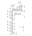
まず、図5~図10を参照して、本発明の第1実施形態について説明する。第1実施形態の磁気メモリ装置100は、STT-MRAM(Spin Transfer Torque Magnetic Random Access Memory)を用いた磁気メモリ装置(以下、「STT-MRAM装置」と呼ぶ。)であり、図5に示すように、メモリセルアレイ110と、選択回路120と、Xデコーダ130と、コントローラ140と、を備える。
<First embodiment>
First, a first embodiment of the present invention will be described with reference to FIGS. 5 to 10. FIG. The magnetic memory device 100 of the first embodiment is a magnetic memory device using STT-MRAM (Spin Transfer Torque Magnetic Random Access Memory) (hereinafter referred to as "STT-MRAM device"), and as shown in FIG. , a memory cell array 110 , a selection circuit 120 , an X decoder 130 and a controller 140 .

メモリセルアレイ110は、クロスポイント型のメモリセルアレイであり、図5に示すように、奇数列のビット線BL1と偶数列のビット線BL2が所定間隔で平行に配列された複数のビット線(複数の配線)と、複数のビット線BL1及びBL2に交差し、所定間隔で平行に配列された複数のワード線WLと、複数のビット線BL1及びBL2と複数のワード線WLとの交点に位置する複数のメモリセル101と、を有する。このように、複数のメモリセル101は、複数のビット線BL1及びBL2の延在方向(図5のy方向)と配列方向(図5のx方向)に沿ってマトリクス状に配置されている。 The memory cell array 110 is a cross-point memory cell array, and as shown in FIG. 5, a plurality of bit lines (a plurality of bit lines) in which odd-numbered bit lines BL1 and even-numbered bit lines BL2 are arranged in parallel at predetermined intervals. ), a plurality of word lines WL intersecting the plurality of bit lines BL1 and BL2 and arranged in parallel at predetermined intervals, and a plurality of word lines WL located at intersections of the plurality of bit lines BL1 and BL2 and the plurality of word lines WL. and a memory cell 101 of . Thus, the plurality of memory cells 101 are arranged in a matrix along the extending direction (y direction in FIG. 5) and arrangement direction (x direction in FIG. 5) of the plurality of bit lines BL1 and BL2.

メモリセル101は、磁気抵抗効果素子としての磁気トンネル接合素子(以下、「MTJ素子」と呼ぶ。)と、MTJ素子をアクセス対象として選択するためのスイッチ素子であるセレクタと、を有している。MTJ素子とセレクタは図5のz方向に積層されている。メモリセル101のMTJ素子は、スピン注入トルク(STT)により磁化反転するMTJ素子であり、強磁性体からなる記録層と、絶縁体からなる障壁層と、強磁性体からなる参照層と、を有する。MTJ素子の記録層、障壁層、及び参照層はこの順もしくはその逆に積層されており、記録層はビット線BL1又はBL2に接続されており、参照層はセレクタに接続されている。セレクタはワード線WLに接続されている。メモリセル101のMTJ素子及びセレクタとして、例えば、非特許文献1に開示されたように、垂直磁化方式のMTJ素子及びHfOxを基本組成とした2端子のセレクタをそれぞれ採用することが可能である。または、メモリセル101のセレクタとして、Si/SiOx/SiN中にCu、Agなどがイオン伝導するイオンブリッジメモリなどで検討されている2端子素子など10以上電流値が変化する2端子素子を採用することも可能である。The memory cell 101 has a magnetic tunnel junction element (hereinafter referred to as an "MTJ element") as a magnetoresistive element, and a selector as a switching element for selecting the MTJ element as an access target. . The MTJ elements and selectors are stacked in the z direction in FIG. The MTJ element of the memory cell 101 is an MTJ element whose magnetization is reversed by spin injection torque (STT), and includes a recording layer made of a ferromagnetic material, a barrier layer made of an insulator, and a reference layer made of a ferromagnetic material. have. The recording layer, barrier layer and reference layer of the MTJ element are stacked in this order or vice versa, the recording layer is connected to the bit line BL1 or BL2, and the reference layer is connected to the selector. The selector is connected to word line WL. As the MTJ element and selector of the memory cell 101, for example, as disclosed in Non-Patent Document 1, a perpendicular magnetization type MTJ element and a two-terminal selector having HfOx as a basic composition can be adopted, respectively. Alternatively, as the selector of the memory cell 101, a two-terminal element that changes the current value by 10 5 or more, such as a two-terminal element that is being studied for an ion bridge memory in which ions such as Cu and Ag are conducted in Si/SiOx/SiN, is adopted. It is also possible to

選択回路120は、第1コントロール線121及び第2コントロール線122を有する。奇数列のビット線BL1は、トランジスタ151を介して第1コントロール線121に接続され、偶数列のビット線BL2は、トランジスタ152を介して第2コントロール線122に接続されている。これらの接続関係の詳細は後述する(図6及び図7参照)。 The selection circuit 120 has a first control line 121 and a second control line 122 . The odd-numbered bit line BL1 is connected to the first control line 121 through the transistor 151, and the even-numbered bit line BL2 is connected to the second control line 122 through the transistor 152. FIG. Details of these connection relationships will be described later (see FIGS. 6 and 7).

Xデコーダ130は、複数のワード線WLに接続されており、コントローラ140の制御の下、アクセス対象の行のワード線WLに電圧を印加する。 The X-decoder 130 is connected to a plurality of word lines WL and applies voltages to the word lines WL of the row to be accessed under the control of the controller 140 .

コントローラ140は、Xデコーダ130と、第1コントロール線121と、第2コントロール線122と、に接続され、データ書き込み又はデータ読み出しに応じて、Xデコーダ130、第1コントロール線121及び第2コントロール線122をそれぞれ制御する。 The controller 140 is connected to the X-decoder 130, the first control line 121, and the second control line 122, and controls the X-decoder 130, the first control line 121, and the second control line according to data write or data read. 122 respectively.

データ書き込み時、コントローラ140は、奇数列のビット線BL1と偶数列のビット線BL2に異なるタイミングで電流を流すように第1コントロール線121及び第2コントロール線122を個別に制御する。ここで「異なるタイミング」とは、隣接するビット線に同時に書き込み電流が流れないように、隣接するビット線の一方に書き込み電流が流れている時と、隣接するビット線の他方に書き込み電流が流れている時が異なっていることを意味する。第2実施形態及び第3実施形態の「異なるタイミング」についても同様である。コントローラ140による書き込み制御の詳細は後述する(図8及び図9参照)。 When writing data, the controller 140 individually controls the first control line 121 and the second control line 122 so that the currents flow through the odd-numbered bit lines BL1 and the even-numbered bit lines BL2 at different timings. Here, "different timing" means that a write current flows through one of the adjacent bit lines and a write current flows through the other of the adjacent bit lines so that the write current does not flow through the adjacent bit lines at the same time. It means that the time is different. The same applies to "different timings" in the second and third embodiments. Details of write control by the controller 140 will be described later (see FIGS. 8 and 9).

次に、図6及び図7を参照して、ビット線BL1と第1コントロール線121との接続、及びビット線BL2と第2コントロール線122との接続について詳細に説明する。 Next, the connection between the bit line BL1 and the first control line 121 and the connection between the bit line BL2 and the second control line 122 will be described in detail with reference to FIGS.

図6は、図5の線VI-VIにおける断面図である。ビット線BL1はトランジスタ151に接続される。トランジスタ151は、電界効果トランジスタであり、ドレイン151bがビット線BL1に接続され、ソース151cが電源線163に接続されている。具体的には、トランジスタ151がビット線BL1よりも下層に設けられており、ビット線BL1は、層間絶縁膜に設けられたスルーホール161a、161b、161c、及び161dと、金属電極層162a、162b、及び162cと、を介して、トランジスタ151のドレイン151bに接続されている。電源線163は、スルーホール161dを介してトランジスタ151のソース151cに接続されている。トランジスタ151のゲート151aは第1コントロール線121に接続されており、ゲート151aに電圧が印加されると、ビット線BL1に電流が流れる。 FIG. 6 is a cross-sectional view taken along line VI-VI of FIG. Bit line BL 1 is connected to transistor 151 . The transistor 151 is a field effect transistor and has a drain 151b connected to the bit line BL1 and a source 151c connected to the power supply line 163 . Specifically, the transistor 151 is provided in a lower layer than the bit line BL1, and the bit line BL1 is connected to through holes 161a, 161b, 161c, and 161d provided in an interlayer insulating film and metal electrode layers 162a and 162b. , and 162c to the drain 151b of the transistor 151. FIG. The power line 163 is connected to the source 151c of the transistor 151 through the through hole 161d. A gate 151a of the transistor 151 is connected to the first control line 121, and when a voltage is applied to the gate 151a, current flows through the bit line BL1.

図7は、図5の線VII-VIIにおける断面図である。ビット線BL2はトランジスタ152に接続される。トランジスタ152は、電界効果トランジスタであり、ドレイン152bがビット線BL2に接続され、ソース152cが電源線173に接続されている。具体的には、トランジスタ152がビット線BL2よりも下層に設けられており、ビット線BL2は、層間絶縁膜に設けられたスルーホール171a、171b、171c、及び171dと、金属電極層172a、172b、及び172cと、を介して、トランジスタ152のドレイン152bに接続されている。電源線173は、スルーホール171dを介してトランジスタ152のソース152cに接続されている。トランジスタ152のゲート152aは第2コントロール線122に接続されており、ゲート152aに電圧が印加されると、ビット線BL2に電流が流れる。 FIG. 7 is a cross-sectional view along line VII-VII of FIG. Bit line BL2 is connected to transistor 152 . The transistor 152 is a field effect transistor and has a drain 152b connected to the bit line BL2 and a source 152c connected to the power supply line 173. FIG. Specifically, the transistor 152 is provided in a lower layer than the bit line BL2, and the bit line BL2 is connected to through holes 171a, 171b, 171c, and 171d provided in the interlayer insulating film, and metal electrode layers 172a and 172b. , and 172c to the drain 152b of the transistor 152. FIG. The power line 173 is connected to the source 152c of the transistor 152 via the through hole 171d. A gate 152a of the transistor 152 is connected to the second control line 122, and when a voltage is applied to the gate 152a, current flows through the bit line BL2.

なお、第1コントロール線121と第2コントロール線122とが別々に設けられていれば、ビット線BL1とトランジスタ151との間を接続するスルーホール及び金属電極層の配置の態様(図6)、並びにビット線BL2とトランジスタ152との間を接続するスルーホール及び金属電極層の配置の態様(図7)は、変更可能である。 Note that if the first control line 121 and the second control line 122 are provided separately, the mode of arrangement of the through hole and the metal electrode layer connecting between the bit line BL1 and the transistor 151 (FIG. 6), Also, the layout of the through-holes connecting the bit line BL2 and the transistor 152 and the metal electrode layer (FIG. 7) can be changed.

次に、図8及び図9を参照して、コントローラ140による書き込み制御について説明する。以下では、奇数列のビット線BL1に接続されたメモリセル101a、101c、及び101eと、偶数列のビット線BL2に接続されたメモリセル101b、101d、及び101fにデータを書き込む例を挙げて説明する。 Next, write control by the controller 140 will be described with reference to FIGS. 8 and 9. FIG. An example of writing data to the memory cells 101a, 101c, and 101e connected to the bit line BL1 of the odd columns and the memory cells 101b, 101d, and 101f connected to the bit lines BL2 of the even columns will be described below. do.

まず、コントローラ140は、書き込むデータに応じて、メモリセル101aに接続されたビット線BL1及びワード線WLの電位、メモリセル101cに接続されたビット線BL1及びワード線WLの電位、並びにメモリセル101eに接続されたビット線BL1及びワード線WLの電位を設定して、メモリセル101a、101c及び101eの各々のセレクタをONにする。また、図8に示すように、第1コントロール線121により、ビット線BL1に接続されたトランジスタ151をONにすることで(すなわち、ゲート151aに電圧を印加することで)、それぞれのビット線BL1を介して、メモリセル101aのMTJ素子、メモリセル101cのMTJ素子、及びメモリセル101eのMTJ素子に書き込み電流Iwを流す。書き込み電流Iwの向きは、ビット線BL1とワード線WLとの電位差により決まる。各MTJ素子に書き込み電流Iwが流れると、スピン注入トルクによって各MTJ素子にデータが書き込まれる。 First, the controller 140 changes the potentials of the bit line BL1 and the word line WL connected to the memory cell 101a, the potentials of the bit line BL1 and the word line WL connected to the memory cell 101c, and the memory cell 101e according to the data to be written. , and the potentials of the bit line BL1 and the word line WL are set to turn ON the selectors of the memory cells 101a, 101c, and 101e. Further, as shown in FIG. 8, by turning on the transistor 151 connected to the bit line BL1 by the first control line 121 (that is, by applying a voltage to the gate 151a), each bit line BL1 is turned on. , a write current Iw is passed through the MTJ element of the memory cell 101a, the MTJ element of the memory cell 101c, and the MTJ element of the memory cell 101e. The direction of the write current Iw is determined by the potential difference between the bit line BL1 and the word line WL. When a write current Iw flows through each MTJ element, data is written into each MTJ element by spin injection torque.

次いで、コントローラ140は、トランジスタ151をOFFにし、書き込むデータに応じて、メモリセル101bに接続されたビット線BL2及びワード線WLの電位、メモリセル101dに接続されたビット線BL2及びワード線WLの電位、並びにメモリセル101fに接続されたビット線BL2及びワード線WLの電位を設定し、メモリセル101b、101d及び101fの各々のセレクタをONにする。また、図9に示すように、第2コントロール線122により、ビット線BL2に接続されたトランジスタ152をONにすることで(すなわち、ゲート152aに電圧を印加することで)、それぞれのビット線BL2を介して、メモリセル101bのMTJ素子、メモリセル101dのMTJ素子、及びメモリセル101fのMTJ素子に書き込み電流Iwを流す。書き込み電流Iwの向きは、ビット線BL2とワード線WLとの電位差により決まる。各MTJ素子に書き込み電流Iwが流れると、スピン注入トルクによって各MTJ素子にデータが書き込まれる。 Next, the controller 140 turns off the transistor 151, and according to the data to be written, the potentials of the bit line BL2 and the word line WL connected to the memory cell 101b and the potentials of the bit line BL2 and the word line WL connected to the memory cell 101d are increased. The potential, the potential of the bit line BL2 and the word line WL connected to the memory cell 101f are set, and the selectors of the memory cells 101b, 101d and 101f are turned on. Further, as shown in FIG. 9, by turning on the transistor 152 connected to the bit line BL2 by the second control line 122 (that is, by applying a voltage to the gate 152a), each bit line BL2 , the write current Iw is passed through the MTJ element of the memory cell 101b, the MTJ element of the memory cell 101d, and the MTJ element of the memory cell 101f. The direction of the write current Iw is determined by the potential difference between the bit line BL2 and the word line WL. When a write current Iw flows through each MTJ element, data is written into each MTJ element by spin injection torque.

なお、奇数列のビット線BL1に書き込み電流を流した後に、偶数列のビット線BL2に書き込み電流を流す例を説明したが、逆の順番にしてもよい。 Although an example has been described in which the write current is applied to the even-numbered bit line BL2 after the write current is applied to the odd-numbered bit line BL1, the order may be reversed.

以上のように、第1実施形態の磁気メモリ装置100によれば、隣接するビット線BL1及びBL2がそれぞれ第1コントロール線121及び第2コントロール線122に接続され、データを書き込むとき、コントローラ140は、非隣接のビット線BL1又は非隣接のビット線BL2に同時に書込み電流を流し、隣接するビット線BL1及びBL2に異なるタイミングで書き込み電流を流すように第1コントロール線121及び第2コントロール線122を個別に制御した。これにより、隣接するビット線BL1及びBL2に同時に書き込み電流が流れることがなく、隣接するメモリセル間において書き込み電流による磁場の影響を低減させ、クロストークの発生を抑制することができる。よって、書き込み電流の値を低減させつつ、低い書き込みエラー率を実現することができる。また、直列接続するメモリセルの数を増やすことができ、製造コストを大幅に増やすことなく、高密度化及び大容量化を図ることができる。さらに、コントロール線ごとにまとめて書き込みをすることができるため、高速の書き込みを実現することができる。 As described above, according to the magnetic memory device 100 of the first embodiment, the adjacent bit lines BL1 and BL2 are connected to the first control line 121 and the second control line 122, respectively. , the first control line 121 and the second control line 122 are arranged so that write currents flow simultaneously through non-adjacent bit lines BL1 or non-adjacent bit lines BL2, and write currents flow through adjacent bit lines BL1 and BL2 at different timings. individually controlled. As a result, the write currents do not flow simultaneously in the adjacent bit lines BL1 and BL2, the influence of the magnetic field caused by the write currents between adjacent memory cells can be reduced, and the occurrence of crosstalk can be suppressed. Therefore, a low write error rate can be achieved while reducing the value of the write current. In addition, the number of memory cells connected in series can be increased, and high density and large capacity can be achieved without significantly increasing the manufacturing cost. Furthermore, since writing can be performed collectively for each control line, high-speed writing can be realized.

なお、図5~図9では、2本のコントロール線を備えた磁気メモリ装置100を示したが、コントロール線の数は2本以上であれば特に限定されない。書き込み電流が大きくなると、2本のコントロール線を個別に制御したとしても漏れ磁場の影響を無視することができなくなる可能性がある。そこで、例えば、図10に示すように、磁気メモリ装置に3本のコントロール線を設けるようにしてもよい。 Although FIGS. 5 to 9 show the magnetic memory device 100 having two control lines, the number of control lines is not particularly limited as long as it is two or more. If the write current becomes large, there is a possibility that the influence of the leakage magnetic field cannot be ignored even if the two control lines are individually controlled. Therefore, for example, as shown in FIG. 10, the magnetic memory device may be provided with three control lines.

図10に示す磁気メモリ装置100Aは、STT-MRAM装置であり、メモリセルアレイ110Aと、選択回路120Aと、Xデコーダ130と、コントローラ140Aと、を備える。 A magnetic memory device 100A shown in FIG. 10 is an STT-MRAM device, and includes a memory cell array 110A, a selection circuit 120A, an X decoder 130, and a controller 140A.

選択回路120Aは、第1コントロール線121、第2コントロール線122、及び第3コントロール線123を有する。 120 A of selection circuits have the 1st control line 121, the 2nd control line 122, and the 3rd control line 123. FIG.

メモリセルアレイ110Aも、メモリセルアレイ110と同様、複数のビット線(ビット線BL1、BL2及びBL3)と複数のワード線WLとの交点にメモリセル101が配置されたクロスポイント型のメモリセルアレイである。メモリセルアレイ110Aにおいて、3n-2列目(nは正の整数)のビット線BL1はトランジスタ151を介して第1コントロール線121に接続され、3n-1列目のビット線BL2はトランジスタ152を介して第2コントロール線122に接続され、3n列目のビット線BL3はトランジスタ153を介して第3コントロール線123に接続されている。トランジスタ151、152及び153は、いずれも電界効果トランジスタである。 Like the memory cell array 110, the memory cell array 110A is also a cross-point type memory cell array in which the memory cells 101 are arranged at intersections of a plurality of bit lines (bit lines BL1, BL2 and BL3) and a plurality of word lines WL. In the memory cell array 110A, the bit line BL1 of the 3n-2th column (n is a positive integer) is connected to the first control line 121 through the transistor 151, and the bit line BL2 of the 3n-1st column is connected through the transistor 152. , and the bit line BL3 on the 3nth column is connected to the third control line 123 via the transistor 153 . Transistors 151, 152 and 153 are all field effect transistors.

コントローラ140Aは、Xデコーダ130と、第1コントロール線121、第2コントロール線122、及び第3コントロール線123と、に接続され、データ書き込み又はデータ読み出しに応じて、Xデコーダ130、第1コントロール線121、第2コントロール線122、及び第3コントロール線123をそれぞれ制御する。 The controller 140A is connected to the X-decoder 130, the first control line 121, the second control line 122, and the third control line 123, and controls the X-decoder 130 and the first control line according to data write or data read. 121, a second control line 122, and a third control line 123, respectively.

メモリセルアレイ110Aにデータを書き込むとき、コントローラ140Aは、隣接するビット線に異なるタイミングで書き込み電流を流すように第1コントロール線121、第2コントロール線122、及び第3コントロール線123を個別に制御する。例えば、まず、第1コントロール線121に接続されたトランジスタ151をONにし、3n-2列目のビット線BL1に書き込み電流を流す。次に、トランジスタ151をOFFにし、第2コントロール線122に接続されたトランジスタ152をONにして、3n-1列目のビット線BL2に書き込み電流を流す。次に、トランジスタ152をOFFにし、第3コントロール線123に接続されたトランジスタ153をONにして、3n列目のビット線BL3に書き込み電流を流す。 When writing data to the memory cell array 110A, the controller 140A individually controls the first control line 121, the second control line 122, and the third control line 123 so that write currents flow to adjacent bit lines at different timings. . For example, first, the transistor 151 connected to the first control line 121 is turned on, and a write current is passed through the bit line BL1 of the 3n-2 column. Next, the transistor 151 is turned off, the transistor 152 connected to the second control line 122 is turned on, and the write current is supplied to the bit line BL2 of the 3n−1 column. Next, the transistor 152 is turned off, the transistor 153 connected to the third control line 123 is turned on, and the write current is supplied to the 3n-th bit line BL3.

図10に示す磁気メモリ装置100Aによれば、より大きな書き込み電流を流す場合であっても、クロストークの発生を抑制することができる。 According to the magnetic memory device 100A shown in FIG. 10, crosstalk can be suppressed even when a larger write current is applied.

<第2実施形態>
次に、図11~図17を参照し、本発明の第2実施形態について説明する。第2実施形態の磁気メモリ装置200は、1トランジスタ(Tra)-1MTJ型のSTT-MRAM装置であり、図11に示すように、メモリセルアレイ210と、選択回路220と、Xデコーダ230と、コントローラ240と、を備える。
<Second embodiment>
Next, a second embodiment of the present invention will be described with reference to FIGS. 11 to 17. FIG. The magnetic memory device 200 of the second embodiment is a 1-transistor (Tra)-1MTJ type STT-MRAM device, and as shown in FIG. 240;

メモリセルアレイ210は、図11に示すように、奇数列のビット線BL1と偶数列のビット線BL2が所定間隔で平行に配列された複数のビット線(複数の配線)と、複数のビット線BL1及びBL2に交差し、所定間隔で平行に配列された複数のワード線WLと、複数のビット線BL1及びBL2と複数のワード線WLとが交差する領域に配置された複数のメモリセル203と、を有する。このように、複数のメモリセル203は、複数のビット線BL1及びBL2の延在方向(図11のy方向)及び配列方向(図11のx方向)に沿ってマトリクス状に配置されている。 As shown in FIG. 11, the memory cell array 210 includes a plurality of bit lines (plurality of wirings) in which odd-numbered bit lines BL1 and even-numbered bit lines BL2 are arranged in parallel at predetermined intervals, and a plurality of bit lines BL1. and BL2 and are arranged in parallel at predetermined intervals; a plurality of memory cells 203 arranged in regions where the plurality of bit lines BL1 and BL2 and the plurality of word lines WL intersect; have Thus, the plurality of memory cells 203 are arranged in a matrix along the extending direction (y direction in FIG. 11) and arrangement direction (x direction in FIG. 11) of the plurality of bit lines BL1 and BL2.

メモリセル203は、磁気抵抗効果素子としてのMTJ素子201と、MTJ素子201をアクセス対象として選択するためのスイッチ素子である選択トランジスタ202と、を有している。MTJ素子201は、スピン注入トルク(STT)により磁化反転するMTJ素子であり、強磁性体からなる記録層と、絶縁体からなる障壁層と、強磁性体からなる参照層と、を有する。MTJ素子201の記録層、障壁層、及び参照層はこの順で積層されており、記録層がビット線BL1又はBL2に接続され、参照層が選択トランジスタ202のドレイン202bに接続されている(図12及び図13参照)。選択トランジスタ202のゲート202aはワード線WLに接続され、ソース202cはソース線266(図12及び図13参照)に接続されている。このように、メモリセル203は、1個の選択トランジスタ202と1個のMTJ素子201とで構成された1Tra-1MTJ型のメモリセルである。 The memory cell 203 has an MTJ element 201 as a magnetoresistive effect element and a selection transistor 202 as a switching element for selecting the MTJ element 201 as an access target. The MTJ element 201 is an MTJ element whose magnetization is reversed by spin injection torque (STT), and has a recording layer made of a ferromagnetic material, a barrier layer made of an insulator, and a reference layer made of a ferromagnetic material. The recording layer, barrier layer, and reference layer of the MTJ element 201 are stacked in this order, the recording layer being connected to the bit line BL1 or BL2, and the reference layer being connected to the drain 202b of the selection transistor 202 (see FIG. 12 and FIG. 13). The select transistor 202 has a gate 202a connected to the word line WL and a source 202c connected to the source line 266 (see FIGS. 12 and 13). Thus, the memory cell 203 is a 1Tra-1MTJ type memory cell composed of one selection transistor 202 and one MTJ element 201 .

選択回路220は、第1コントロール線221及び第2コントロール線222を有する。奇数列のビット線BL1は、トランジスタ251を介して第1コントロール線221に接続され、偶数列のビット線BL2は、トランジスタ252を介して第2コントロール線222に接続されている。これらの接続関係の詳細は後述する(図12及び図13参照)。 The selection circuit 220 has a first control line 221 and a second control line 222 . The odd-numbered bit lines BL1 are connected to the first control line 221 through the transistors 251, and the even-numbered bit lines BL2 are connected to the second control lines 222 through the transistors 252. FIG. Details of these connection relationships will be described later (see FIGS. 12 and 13).

Xデコーダ230は、複数のワード線WL及び複数のソース線266に接続されており、コントローラ240の制御の下、アクセス対象の行のワード線WL及びソース線266のそれぞれに電圧を印加する。 The X-decoder 230 is connected to a plurality of word lines WL and a plurality of source lines 266 and applies voltages to the word lines WL and source lines 266 of the row to be accessed under the control of the controller 240 .

コントローラ240は、Xデコーダ230と、第1コントロール線221と、第2コントロール線222と、に接続され、データ書き込み又はデータ読み出しに応じて、Xデコーダ230、第1コントロール線221及び第2コントロール線222をそれぞれ制御する。 The controller 240 is connected to the X-decoder 230, the first control line 221, and the second control line 222, and controls the X-decoder 230, the first control line 221, and the second control line according to data write or data read. 222 respectively.

データ書き込み時、コントローラ240は、奇数列のビット線BL1と偶数列のビット線BL2に異なるタイミングで書き込み電流を流すように第1コントロール線221及び第2コントロール線222を個別に制御する。コントローラ240による書き込み制御については後述する。 When writing data, the controller 240 individually controls the first control line 221 and the second control line 222 so that write currents flow through the odd-numbered bit lines BL1 and the even-numbered bit lines BL2 at different timings. Write control by the controller 240 will be described later.

次に、図12及び図13を参照して、ビット線BL1と第1コントロール線221との接続、ビット線BL2と第2コントロール線222との接続、及びMTJ素子201と対応する選択トランジスタ202との接続について詳細に説明する。 Next, referring to FIGS. 12 and 13, the connection between bit line BL1 and first control line 221, the connection between bit line BL2 and second control line 222, and the connection between MTJ element 201 and corresponding select transistor 202. connection will be described in detail.

図12は、図11の線XII-XIIにおける断面図である。ビット線BL1はトランジスタ251に接続される。トランジスタ251は、電界効果トランジスタであり、ドレイン251bがビット線BL1に接続され、ソース251cが電源線263に接続されている。具体的には、トランジスタ251がビット線BL1よりも下層に設けられており、ビット線BL1は、層間絶縁膜に設けられたスルーホール261a、261b、261c、及び261dと、金属電極層262a、262b、及び262cと、を介して、トランジスタ251のドレイン251bに接続されている。電源線263は、スルーホール261dを介してトランジスタ251のソース251cに接続されている。トランジスタ251のゲート251aは第1コントロール線221に接続されており、ゲート251aに電圧が印加されると、ビット線BL1に電流が流れる。 12 is a cross-sectional view taken along line XII-XII of FIG. 11. FIG. Bit line BL 1 is connected to transistor 251 . The transistor 251 is a field effect transistor and has a drain 251b connected to the bit line BL1 and a source 251c connected to the power supply line 263 . Specifically, the transistor 251 is provided in a lower layer than the bit line BL1, and the bit line BL1 is connected to through holes 261a, 261b, 261c, and 261d provided in an interlayer insulating film and metal electrode layers 262a and 262b. , and 262c to the drain 251b of the transistor 251. FIG. The power line 263 is connected to the source 251c of the transistor 251 through the through hole 261d. A gate 251a of the transistor 251 is connected to the first control line 221, and when a voltage is applied to the gate 251a, current flows through the bit line BL1.

ビット線BL1に接続されたMTJ素子201は、層間絶縁膜に設けられたスルーホール265b、265c、及び265dと、金属電極層264a、264b、及び264cと、を介して、選択トランジスタ202のドレイン202bに接続されている。選択トランジスタ202のソース202cはスルーホール265dを介してソース線266に接続され、ゲート202aはワード線WLに接続されている。選択トランジスタ202とトランジスタ251は、半導体基板の活性領域に形成されており、これらの活性領域は素子分離領域により区画されている。 The MTJ element 201 connected to the bit line BL1 is connected to the drain 202b of the select transistor 202 through through holes 265b, 265c, and 265d provided in the interlayer insulating film and metal electrode layers 264a, 264b, and 264c. It is connected to the. The source 202c of the select transistor 202 is connected to the source line 266 via the through hole 265d, and the gate 202a is connected to the word line WL. The selection transistor 202 and the transistor 251 are formed in active regions of a semiconductor substrate, and these active regions are partitioned by element isolation regions.

図13は、図11の線XIII-XIIIにおける断面図である。ビット線BL2はトランジスタ252に接続される。トランジスタ252は、電界効果トランジスタであり、ドレイン252bがビット線BL2に接続され、ソース252cが電源線273に接続されている。具体的には、トランジスタ252がビット線BL2よりも下層に設けられており、ビット線BL2は、層間絶縁膜に設けられたスルーホール271a、271b、271c、及び271dと、金属電極層272a、272b、及び272cと、を介して、トランジスタ252のドレイン252bに接続されている。電源線273は、スルーホール271dを介してトランジスタ252のソース252cに接続されている。トランジスタ252のゲート252aは第2コントロール線222に接続されており、ゲート252aに電圧が印加されると、ビット線BL2に電流が流れる。 13 is a cross-sectional view along line XIII-XIII of FIG. 11. FIG. Bit line BL2 is connected to transistor 252 . The transistor 252 is a field effect transistor and has a drain 252b connected to the bit line BL2 and a source 252c connected to the power supply line 273. FIG. Specifically, the transistor 252 is provided in a lower layer than the bit line BL2, and the bit line BL2 is connected to through holes 271a, 271b, 271c, and 271d provided in the interlayer insulating film and metal electrode layers 272a and 272b. , and 272c to the drain 252b of the transistor 252. FIG. The power line 273 is connected to the source 252c of the transistor 252 via the through hole 271d. A gate 252a of the transistor 252 is connected to the second control line 222, and when a voltage is applied to the gate 252a, a current flows through the bit line BL2.

ビット線BL2に接続されたMTJ素子201は、層間絶縁膜に設けられたスルーホール275b、275c、及び275dと、金属電極層274a、274b、及び274cと、を介して、選択トランジスタ202のドレイン202bに接続されている。選択トランジスタ202のソース202cはスルーホール275dを介してソース線266に接続され、ゲート202aはワード線WLに接続されている。選択トランジスタ202とトランジスタ252は、半導体基板の活性領域に形成されており、これらの活性領域は素子分離領域により区画されている。 The MTJ element 201 connected to the bit line BL2 is connected to the drain 202b of the selection transistor 202 through through holes 275b, 275c, and 275d provided in the interlayer insulating film and metal electrode layers 274a, 274b, and 274c. It is connected to the. The source 202c of the select transistor 202 is connected to the source line 266 via the through hole 275d, and the gate 202a is connected to the word line WL. The selection transistor 202 and the transistor 252 are formed in active regions of a semiconductor substrate, and these active regions are partitioned by element isolation regions.

なお、第1コントロール線221と第2コントロール線222とが別々に設けられていれば、ビット線BL1とトランジスタ251との間を接続するスルーホール及び金属電極層の配置の態様(図12)、並びにビット線BL2とトランジスタ252との間を接続するスルーホール及び金属電極層の配置の態様(図13)は、変更可能である。 Note that if the first control line 221 and the second control line 222 are provided separately, the mode of arrangement of the through hole and the metal electrode layer connecting between the bit line BL1 and the transistor 251 (FIG. 12), Also, the layout of the through-holes connecting the bit line BL2 and the transistor 252 and the metal electrode layer (FIG. 13) can be changed.

次に、コントローラ240による書き込み制御について説明する。以下では、奇数列のビット線BL1に書き込み電流を流した後に、偶数列のビット線BL2に書き込み電流を流すものとして説明するが、逆の順番にしてもよい。 Next, write control by the controller 240 will be described. In the following description, it is assumed that the write current is applied to the even-numbered bit line BL2 after the write current is applied to the odd-numbered bit line BL1, but the order may be reversed.

まず、コントローラ240は、書き込むデータに応じて、書き込み対象のメモリセル203が接続された奇数列のビット線BL1の電位、及び当該メモリセル203の選択トランジスタ202のソース202c(ソース線266)の電位を設定する。ビット線BL1と選択トランジスタ202のソース202cとの電位差により、書き込み電流の向きが決まる。また、コントローラ240は、当該メモリセル203に対応するワード線WLから選択トランジスタ202のゲート202aに電圧を印加させて選択トランジスタ202をONにするとともに、第1コントロール線221により、ビット線BL1に接続されたトランジスタ251をONにする。これにより、ビット線BL1及びMTJ素子201に書き込み電流が流れ、スピン注入トルクによってMTJ素子201の磁化が反転し、データが書き込まれる。 First, the controller 240 changes the potential of the odd-numbered bit line BL1 to which the memory cell 203 to be written is connected and the potential of the source 202c (source line 266) of the select transistor 202 of the memory cell 203 according to the data to be written. set. The potential difference between the bit line BL1 and the source 202c of the select transistor 202 determines the direction of the write current. In addition, the controller 240 applies a voltage from the word line WL corresponding to the memory cell 203 to the gate 202a of the select transistor 202 to turn on the select transistor 202, and connects it to the bit line BL1 through the first control line 221. The transistor 251 is turned on. As a result, a write current flows through the bit line BL1 and the MTJ element 201, the magnetization of the MTJ element 201 is reversed by spin injection torque, and data is written.

次いで、コントローラ240は、トランジスタ251をOFFにし、書き込むデータに応じて、書き込み対象のメモリセル203が接続された偶数列のビット線BL2の電位、及び当該メモリセル203の選択トランジスタ202のソース202c(ソース線266)の電位を設定する。ビット線BL2と選択トランジスタ202のソース202cとの電位差により、書き込み電流の向きが決まる。また、コントローラ240は、当該メモリセル203に対応するワード線WLから選択トランジスタ202のゲート202aに電圧を印加させて選択トランジスタ202をONにするとともに、第2コントロール線222により、ビット線BL2に接続されたトランジスタ252をONにする。これにより、ビット線BL2及びMTJ素子201に書き込み電流が流れ、スピン注入トルクによってMTJ素子201の磁化が反転し、データが書き込まれる。 Next, the controller 240 turns off the transistor 251, and according to the data to be written, the potential of the bit line BL2 in the even column connected to the memory cell 203 to be written and the source 202c ( Set the potential of the source line 266). The potential difference between the bit line BL2 and the source 202c of the select transistor 202 determines the direction of the write current. In addition, the controller 240 applies a voltage from the word line WL corresponding to the memory cell 203 to the gate 202a of the selection transistor 202 to turn on the selection transistor 202, and also connects it to the bit line BL2 through the second control line 222. turn on the transistor 252 that is turned on. As a result, a write current flows through the bit line BL2 and the MTJ element 201, the magnetization of the MTJ element 201 is reversed by spin injection torque, and data is written.

第2実施形態の磁気メモリ装置200によれば、第1実施形態の磁気メモリ装置100と同様の効果を得ることができる。磁気メモリ装置200は、各メモリセル203が選択トランジスタ202を有していることから、図11のy方向におけるメモリセル203の配置は、クロスポイント型の磁気メモリ装置100のメモリセル101の配置に比べると密ではない。しかしながら、大容量の磁気メモリ装置200では、ビット線BL1及びBL2の配列方向(図11のx方向)においてメモリセル203は密に配置されることから、第2実施形態のように、第1コントロール線221及び第2コントロール線222を個別に制御して、隣接するビット線に異なるタイミングで電流を流すことは有効である。 According to the magnetic memory device 200 of the second embodiment, effects similar to those of the magnetic memory device 100 of the first embodiment can be obtained. Since each memory cell 203 of the magnetic memory device 200 has a selection transistor 202, the arrangement of the memory cells 203 in the y direction in FIG. not dense in comparison. However, in the large-capacity magnetic memory device 200, the memory cells 203 are densely arranged in the arrangement direction of the bit lines BL1 and BL2 (the x direction in FIG. 11). It is effective to individually control the line 221 and the second control line 222 so that currents flow in adjacent bit lines at different timings.

なお、図11~図13では、2本のコントロール線を備えた磁気メモリ装置200を示したが、コントロール線の数は2本以上であれば特に限定されない。書き込み電流が大きくなると、2本のコントロール線を個別に制御したとしても漏れ磁場の影響を無視することができなくなる可能性がある。そこで、例えば、図14に示すように、磁気メモリ装置に3本のコントロール線を設けるようにしてもよい。 11 to 13 show the magnetic memory device 200 having two control lines, the number of control lines is not particularly limited as long as it is two or more. If the write current becomes large, there is a possibility that the influence of the leakage magnetic field cannot be ignored even if the two control lines are individually controlled. Therefore, for example, as shown in FIG. 14, the magnetic memory device may be provided with three control lines.

図14に示す磁気メモリ装置200Aは、STT-MRAM装置であり、メモリセルアレイ210Aと、選択回路220Aと、Xデコーダ230と、コントローラ240Aと、を備える。 A magnetic memory device 200A shown in FIG. 14 is an STT-MRAM device, and includes a memory cell array 210A, a selection circuit 220A, an X decoder 230, and a controller 240A.

選択回路220Aは、第1コントロール線221、第2コントロール線222、及び第3コントロール線223を有する。 220 A of selection circuits have the 1st control line 221, the 2nd control line 222, and the 3rd control line 223. FIG.

メモリセルアレイ210Aを構成するメモリセル203も、1個のMTJ素子201と1個の選択トランジスタ202とからなる1Tra-1MTJ型のメモリセルである。メモリセルアレイ210Aにおいて、3n-2列目(nは正の整数)のビット線BL1はトランジスタ251を介して第1コントロール線221に接続され、3n-1列目のビット線BL2はトランジスタ252を介して第2コントロール線222に接続され、3n列目のビット線BL3はトランジスタ253を介して第3コントロール線223に接続されている。トランジスタ251、252及び253は、いずれも電界効果トランジスタである。 A memory cell 203 forming the memory cell array 210A is also a 1Tra-1MTJ type memory cell composed of one MTJ element 201 and one selection transistor 202 . In the memory cell array 210A, the bit line BL1 of the 3n-2th column (n is a positive integer) is connected to the first control line 221 through the transistor 251, and the bit line BL2 of the 3n-1th column is connected through the transistor 252. The bit line BL3 on the 3nth column is connected to the third control line 223 via the transistor 253. Transistors 251, 252 and 253 are all field effect transistors.

コントローラ240Aは、Xデコーダ230と、第1コントロール線221、第2コントロール線222、及び第3コントロール線223と、に接続され、データ書き込み又はデータ読み出しに応じて、Xデコーダ230、第1コントロール線221、第2コントロール線222、及び第3コントロール線223をそれぞれ制御する。 The controller 240A is connected to the X-decoder 230, the first control line 221, the second control line 222, and the third control line 223, and controls the X-decoder 230 and the first control line according to data write or data read. 221, the second control line 222 and the third control line 223 respectively.

メモリセルアレイ210Aにデータを書き込むとき、コントローラ240Aは、隣接するビット線に異なるタイミングで書き込み電流を流すように第1コントロール線221、第2コントロール線222、及び第3コントロール線223を個別に制御する。例えば、まず、第1コントロール線221に接続されたトランジスタ251をONにして、3n-2列目のビット線BL1に書き込み電流を流す。次に、トランジスタ251をOFFにし、第2コントロール線222に接続されたトランジスタ252をONにして、3n-1列目のビット線BL2に書き込み電流を流す。次に、トランジスタ252をOFFにし、第3コントロール線223に接続されたトランジスタ253をONにして、3n列目のビット線BL3に書き込み電流を流す。 When writing data to the memory cell array 210A, the controller 240A individually controls the first control line 221, the second control line 222, and the third control line 223 so that write currents flow to adjacent bit lines at different timings. . For example, first, the transistor 251 connected to the first control line 221 is turned on to supply a write current to the 3n-2-th bit line BL1. Next, the transistor 251 is turned off, the transistor 252 connected to the second control line 222 is turned on, and the write current is supplied to the bit line BL2 of the 3n−1 column. Next, the transistor 252 is turned off, the transistor 253 connected to the third control line 223 is turned on, and the write current is supplied to the 3n-th bit line BL3.

図14に示す磁気メモリ装置200Aによれば、より大きな書き込み電流を流す場合であっても、クロストークの発生を抑制することができる。 According to the magnetic memory device 200A shown in FIG. 14, crosstalk can be suppressed even when a larger write current is applied.

図11~図13に示す磁気メモリ装置200及び図14に示す磁気メモリ装置200Aでは、メモリセルアレイの1行につき1本のソース線266を設けているが、図15~図17に示すように、隣接する2行ごとに1本のソース線を設けるようにしてもよい。 In the magnetic memory device 200 shown in FIGS. 11 to 13 and the magnetic memory device 200A shown in FIG. 14, one source line 266 is provided for each row of the memory cell array. One source line may be provided for every two adjacent rows.

図15に示す磁気メモリ装置200Bは、STT-MRAM装置であり、メモリセルアレイ210Bと、選択回路220Bと、Xデコーダ230Bと、コントローラ240Bと、を備えている。 A magnetic memory device 200B shown in FIG. 15 is an STT-MRAM device, and includes a memory cell array 210B, a selection circuit 220B, an X decoder 230B, and a controller 240B.

選択回路220Bは、第1コントロール線221及び第2コントロール線222を有する。 The selection circuit 220B has a first control line 221 and a second control line 222 .

コントローラ240Bは、Xデコーダ230Bと、第1コントロール線221と、第2コントロール線222と、に接続され、データ書き込み又はデータ読み出しに応じて、Xデコーダ230B、第1コントロール線221及び第2コントロール線222をそれぞれ制御する。 The controller 240B is connected to the X-decoder 230B, the first control line 221, and the second control line 222, and controls the X-decoder 230B, the first control line 221, and the second control line according to data write or data read. 222 respectively.

磁気メモリ装置200Bは、メモリセルアレイ210Bの隣接する2行ごとに1本のソース線276を設ける点で図11~図13に示す磁気メモリ装置200と異なる。奇数列のビット線BL1と第1コントロール線221との接続関係、偶数列のビット線BL2と第2コントロール線222との接続関係、及びコントローラ240Bによる書き込み制御については、磁気メモリ装置200と同様であるため、その説明を省略する。以下、磁気メモリ装置200の構造と異なる点のみを説明する。 The magnetic memory device 200B differs from the magnetic memory device 200 shown in FIGS. 11 to 13 in that one source line 276 is provided for every two adjacent rows of the memory cell array 210B. The connection relationship between the odd-numbered bit lines BL1 and the first control lines 221, the connection relationship between the even-numbered bit lines BL2 and the second control lines 222, and the write control by the controller 240B are the same as those of the magnetic memory device 200. Therefore, the description is omitted. Only the points that differ from the structure of the magnetic memory device 200 will be described below.

図16は、図15の線XVI-XVIにおける断面図である。ビット線BL1に接続されたMTJ素子201は、層間絶縁膜に設けられたスルーホール265b、265c、及び265dと、金属電極層264a、264b、及び264cと、を介して、選択トランジスタ202のドレイン202bに接続されている。選択トランジスタ202のソース202cはスルーホール265dを介してソース線276に接続され、ゲート202aはワード線WLに接続されている。行方向(図16のy方向)で隣接する2個の選択トランジスタ202は、ソース202cを共有しており、共通のソース線276に接続されている。選択トランジスタ202は、半導体基板の活性領域に形成されており、活性領域は素子分離領域により区画されている。 16 is a cross-sectional view along line XVI-XVI of FIG. 15. FIG. The MTJ element 201 connected to the bit line BL1 is connected to the drain 202b of the select transistor 202 through through holes 265b, 265c, and 265d provided in the interlayer insulating film and metal electrode layers 264a, 264b, and 264c. It is connected to the. The source 202c of the select transistor 202 is connected to the source line 276 via the through hole 265d, and the gate 202a is connected to the word line WL. Two select transistors 202 adjacent in the row direction (y direction in FIG. 16) share a source 202c and are connected to a common source line 276 . The selection transistor 202 is formed in an active region of a semiconductor substrate, and the active region is partitioned by an isolation region.

図17は、図15の線XVII-XVIIにおける断面図である。ビット線BL2に接続されたMTJ素子201は、層間絶縁膜に設けられたスルーホール275b、275c、及び275dと、金属電極層274a、274b、及び274cと、を介して、選択トランジスタ202のドレイン202bに接続されている。選択トランジスタ202のソース202cはスルーホール275dを介してソース線276に接続され、ゲート202aはワード線WLに接続されている。行方向(図17のy方向)で隣接する2個の選択トランジスタ202は、ソース202cを共有しており、共通のソース線276に接続されている。選択トランジスタ202は、半導体基板の活性領域に形成されており、これらの活性領域は素子分離領域により区画されている。 17 is a cross-sectional view along line XVII-XVII of FIG. 15. FIG. The MTJ element 201 connected to the bit line BL2 is connected to the drain 202b of the selection transistor 202 through through holes 275b, 275c, and 275d provided in the interlayer insulating film and metal electrode layers 274a, 274b, and 274c. It is connected to the. The source 202c of the select transistor 202 is connected to the source line 276 via the through hole 275d, and the gate 202a is connected to the word line WL. Two select transistors 202 adjacent in the row direction (y direction in FIG. 17) share a source 202c and are connected to a common source line 276 . The selection transistor 202 is formed in active regions of a semiconductor substrate, and these active regions are partitioned by element isolation regions.

このように、メモリセルアレイ210Bの行方向で隣接する2個の選択トランジスタ202ごとにソース202cを共有することで、行方向においてメモリセル203をより密に配置することができ、大容量化を図ることができる。 By sharing the source 202c for every two select transistors 202 adjacent in the row direction of the memory cell array 210B in this way, the memory cells 203 can be arranged more densely in the row direction, and the capacity can be increased. be able to.

なお、言うまでもなく、図15~図17の磁気メモリ装置200Bにおいて、3本以上のコントロール線を備えるようにしてもよい。 Needless to say, the magnetic memory device 200B of FIGS. 15 to 17 may be provided with three or more control lines.

<第3実施形態>
次に、図18~図21を参照して本発明の第3実施形態について説明する。第3実施形態の磁気メモリ装置300は、SOT-MRAM(Spin-Orbit Torque Magnetic Random Access Memory)を用いた磁気メモリ装置(以下、「SOT-MRAM装置」と呼ぶ。)であり、図18に示すように、メモリセルアレイ310と、選択回路320と、Xデコーダ330と、コントローラ340と、を備える。
<Third Embodiment>
Next, a third embodiment of the present invention will be described with reference to FIGS. 18 to 21. FIG. The magnetic memory device 300 of the third embodiment is a magnetic memory device using SOT-MRAM (Spin-Orbit Torque Magnetic Random Access Memory) (hereinafter referred to as "SOT-MRAM device"), and is shown in FIG. As shown, a memory cell array 310, a selection circuit 320, an X-decoder 330, and a controller 340 are provided.

メモリセルアレイ310では、図18に示すように、一方向(図18のy方向)に延在した細長形状を有する複数の重金属層(複数の配線)が所定間隔で平行に配列されている。複数の重金属層は、奇数列の重金属層31_1と偶数列の重金属層31_2からなる。各重金属層31_1上には、一定数のメモリセル303が重金属層31_1の長手方向(図18のy方向)に沿って直列に配置され、各重金属層31_2上には、一定数のメモリセル303が重金属層31_2の長手方向(図18のy方向)に沿って直列に配置されている。このように、複数のメモリセル303は、複数の重金属層の延在方向(y方向)及び配列方向(x方向)に沿ってマトリクス状に配置されている。 In the memory cell array 310, as shown in FIG. 18, a plurality of heavy metal layers (plurality of wirings) having an elongated shape extending in one direction (the y direction in FIG. 18) are arranged in parallel at predetermined intervals. The plurality of heavy metal layers are composed of odd-numbered heavy metal layers 31_1 and even-numbered heavy metal layers 31_2. A certain number of memory cells 303 are arranged in series along the longitudinal direction of the heavy metal layer 31_1 (the y direction in FIG. 18) on each heavy metal layer 31_1, and a certain number of memory cells 303 are arranged on each heavy metal layer 31_2. are arranged in series along the longitudinal direction (y direction in FIG. 18) of the heavy metal layer 31_2. In this manner, the plurality of memory cells 303 are arranged in a matrix along the extending direction (y direction) and arrangement direction (x direction) of the plurality of heavy metal layers.

メモリセル303は、磁気抵抗効果素子としてのMTJ素子301と、MTJ素子301上に形成された電極302と、を有する。MTJ素子301は、強磁性体からなる記録層と、絶縁体からなる障壁層と、強磁性体からなる参照層と、を有し、スピン軌道トルク(SOT)により磁化反転するMTJ素子である。MTJ素子301の記録層、障壁層、及び参照層はこの順で積層されており、記録層は重金属層31_1又は重金属層31_2と接しており、参照層は電極302に接続されている。 The memory cell 303 has an MTJ element 301 as a magnetoresistive element and an electrode 302 formed on the MTJ element 301 . The MTJ element 301 has a recording layer made of ferromagnetic material, a barrier layer made of insulating material, and a reference layer made of ferromagnetic material, and is an MTJ element whose magnetization is reversed by spin-orbit torque (SOT). The recording layer, barrier layer, and reference layer of the MTJ element 301 are stacked in this order, the recording layer being in contact with the heavy metal layer 31_1 or heavy metal layer 31_2, and the reference layer being connected to the electrode 302 .

選択回路320は、第1コントロール線321及び第2コントロール線322を有する。奇数列の重金属層31_1は、トランジスタ351を介して第1コントロール線321に接続され、偶数列の重金属層31_2は、トランジスタ352を介して第2コントロール線322に接続されている。これらの接続関係の詳細は後述する(図19及び図20参照)。 The selection circuit 320 has a first control line 321 and a second control line 322 . The heavy metal layers 31_1 in odd columns are connected to the first control line 321 via transistors 351, and the heavy metal layers 31_2 in even columns are connected to the second control line 322 via transistors 352. FIG. Details of these connection relationships will be described later (see FIGS. 19 and 20).

Xデコーダ330は、メモリセル選択用の複数の選択線(図示せず)に接続されており、コントローラ340の制御の下、アクセス対象の選択線を介して電極302に電圧を印加する。 The X-decoder 330 is connected to a plurality of select lines (not shown) for selecting memory cells and, under the control of the controller 340, applies voltages to the electrodes 302 via the select lines to be accessed.

コントローラ340は、Xデコーダ330と、第1コントロール線321と、第2コントロール線322と、に接続され、データ書き込み又はデータ読み出しに応じて、Xデコーダ330、第1コントロール線321及び第2コントロール線322をそれぞれ制御する。 The controller 340 is connected to the X-decoder 330, the first control line 321, and the second control line 322, and controls the X-decoder 330, the first control line 321, and the second control line 321 according to data write or data read. 322 respectively.

データ書き込み時、コントローラ340は、奇数列の重金属層31_1と偶数列の重金属層31_2に異なるタイミングで書き込み電流を流すように第1コントロール線321及び第2コントロール線322を個別に制御する。コントローラ340による書き込み制御については後述する。 When writing data, the controller 340 individually controls the first control line 321 and the second control line 322 so that write currents flow through the odd-column heavy metal layers 31_1 and the even-column heavy metal layers 31_2 at different timings. Write control by the controller 340 will be described later.

次に、図19及び図20を参照して、重金属層31_1と第1コントロール線321との接続、及び重金属層31_2と第2コントロール線322との接続について詳細に説明する。 Next, the connection between the heavy metal layer 31_1 and the first control line 321 and the connection between the heavy metal layer 31_2 and the second control line 322 will be described in detail with reference to FIGS. 19 and 20. FIG.

図19は、図18の線XIX-XIXにおける断面図である。重金属層31_1は、一端がスルーホール361aを介してグラウンドに接続され、他端がトランジスタ351に接続されている。トランジスタ351は、電界効果トランジスタであり、ドレイン351bが重金属層31_1に接続され、ソース351cが電源線363に接続されている。具体的には、トランジスタ351が重金属層31_1よりも下層に設けられており、重金属層31_1は、層間絶縁膜に設けられたスルーホール361a、361b、361c、及び361dと、金属電極層362a、362b、及び362cと、を介して、トランジスタ351のドレイン351bに接続されている。電源線363は、スルーホール361dを介してトランジスタ351のソース351cに接続されている。トランジスタ351のゲート351aは第1コントロール線321に接続されており、ゲート351aに電圧が印加されると、重金属層31_1に電流が流れる。 19 is a cross-sectional view along line XIX-XIX of FIG. 18. FIG. The heavy metal layer 31_1 has one end connected to the ground via the through hole 361a and the other end connected to the transistor 351 . The transistor 351 is a field effect transistor and has a drain 351b connected to the heavy metal layer 31_1 and a source 351c connected to the power supply line 363 . Specifically, the transistor 351 is provided in a lower layer than the heavy metal layer 31_1. , and 362c to the drain 351b of the transistor 351. FIG. The power line 363 is connected to the source 351c of the transistor 351 via the through hole 361d. A gate 351a of the transistor 351 is connected to the first control line 321, and when a voltage is applied to the gate 351a, current flows through the heavy metal layer 31_1.

図20は、図18の線XX-XXにおける断面図である。重金属層31_2は、一端がスルーホール371aを介してグラウンドに接続され、他端がトランジスタ352に接続されている。トランジスタ352は、電界効果トランジスタであり、ドレイン352bが重金属層31_2に接続され、ソース352cが電源線373に接続されている。具体的には、トランジスタ352が重金属層31_2よりも下層に設けられており、重金属層31_2は、層間絶縁膜に設けられたスルーホール371a、371b、371c、及び371dと、金属電極層372a、372b、及び372cと、を介して、トランジスタ352のドレイン352bに接続されている。電源線373は、スルーホール371dを介してトランジスタ352のソース352cに接続されている。トランジスタ352のゲート352aは第2コントロール線322に接続されており、ゲート352aに電圧が印加されると、重金属層31_2に電流が流れる。 20 is a cross-sectional view taken along line XX-XX of FIG. 18. FIG. The heavy metal layer 31_2 has one end connected to the ground via the through hole 371a and the other end connected to the transistor 352 . The transistor 352 is a field effect transistor and has a drain 352b connected to the heavy metal layer 31_2 and a source 352c connected to the power supply line 373 . Specifically, the transistor 352 is provided in a lower layer than the heavy metal layer 31_2. , and 372c to the drain 352b of the transistor 352. FIG. The power line 373 is connected to the source 352c of the transistor 352 through the through hole 371d. A gate 352a of the transistor 352 is connected to the second control line 322, and when a voltage is applied to the gate 352a, current flows through the heavy metal layer 31_2.

なお、第1コントロール線321と第2コントロール線322とが別々に設けられていれば、重金属層31_1とトランジスタ351との間を接続するスルーホール及び金属電極層の配置の態様(図19)、並びに重金属層31_2とトランジスタ352との間を接続するスルーホール及び金属電極層の配置の態様(図20)は、変更可能である。 In addition, if the first control line 321 and the second control line 322 are provided separately, the mode of arrangement of the through hole and the metal electrode layer connecting between the heavy metal layer 31_1 and the transistor 351 (FIG. 19), Also, the mode of arrangement of the through holes connecting between the heavy metal layer 31_2 and the transistor 352 and the metal electrode layer (FIG. 20) can be changed.

次に、コントローラ340による書き込み制御について説明する。以下では、奇数列の重金属層31_1に書き込み電流を流した後に、偶数列の重金属層31_2に書き込み電流を流すものとして説明するが、逆の順番にしてもよい。 Next, write control by the controller 340 will be described. In the following description, it is assumed that the write current is applied to the heavy metal layers 31_1 in the odd columns and then the heavy metal layers 31_2 in the even columns, but the order may be reversed.

まず、コントローラ340は、書き込むデータに応じて、電源線363の電位を設定し、第1コントロール線321によりトランジスタ351をONにすることで(すなわち、ゲート351aに電圧を印加することで)、重金属層31_1に書き込み電流を流す。ここで、電源線363の電位をグラウンドよりLowレベルに設定した場合、書き込み電流は図18及び図19の-y方向に流れ、電源線363の電位をグラウンドよりHighレベルに設定した場合、書き込み電流は図18及び図19の+y方向に流れる。また、コントローラ340は、当該重金属層31_1上に配置された書き込み対象のメモリセル303の電極302から、対応するMTJ素子301の参照層に電圧を印加させる。これにより、当該MTJ素子301の記録層の磁気異方性が下がり、データが書き込まれる。 First, the controller 340 sets the potential of the power supply line 363 in accordance with the data to be written, and turns on the transistor 351 by the first control line 321 (that is, by applying a voltage to the gate 351a), so that the heavy metal A write current is passed through the layer 31_1. Here, when the potential of the power supply line 363 is set at a level lower than the ground, the write current flows in the -y direction in FIGS. flows in the +y direction in FIGS. Further, the controller 340 applies a voltage to the reference layer of the corresponding MTJ element 301 from the electrode 302 of the write target memory cell 303 arranged on the heavy metal layer 31_1. As a result, the magnetic anisotropy of the recording layer of the MTJ element 301 is lowered, and data is written.

次いで、コントローラ340は、トランジスタ351をOFFにし、書き込むデータに応じて、電源線373の電位を設定し、第2コントロール線322によりトランジスタ352をONにすることで(すなわち、ゲート352aに電圧を印加することで)、重金属層31_2に書き込み電流を流す。ここで、電源線373の電位をグラウンドよりLowレベルに設定した場合、書き込み電流は図18及び図20の-y方向に流れ、電源線373の電位をグラウンドよりHighレベルに設定した場合、書き込み電流は図18及び図20の+y方向に流れる。また、コントローラ340は、当該重金属層31_2上に配置された書き込み対象のメモリセル303の電極302から、対応するMTJ素子301の参照層に電圧を印加させる。これにより、当該MTJ素子301の記録層の磁気異方性が下がり、データが書き込まれる。 Next, the controller 340 turns off the transistor 351, sets the potential of the power supply line 373 according to the data to be written, and turns on the transistor 352 by the second control line 322 (that is, by applying a voltage to the gate 352a). ), a write current is passed through the heavy metal layer 31_2. Here, when the potential of the power supply line 373 is set at a level lower than the ground, the write current flows in the -y direction in FIGS. flows in the +y direction in FIGS. Further, the controller 340 applies a voltage to the reference layer of the corresponding MTJ element 301 from the electrode 302 of the write target memory cell 303 arranged on the heavy metal layer 31_2. As a result, the magnetic anisotropy of the recording layer of the MTJ element 301 is lowered, and data is written.

第3実施形態の磁気メモリ装置300によれば、第1実施形態の磁気メモリ装置100及び第2実施形態の磁気メモリ装置200とほぼ同様の効果を得ることができる。特に、磁気メモリ装置300は、コントロール線ごとに一括書き込みが可能なため、より高速な書き込みが可能となる。また、一括書き込みにより、1個のメモリセル303あたりの書き込み電流を下げることができ、消費電力を削減することができる。 According to the magnetic memory device 300 of the third embodiment, substantially the same effects as those of the magnetic memory device 100 of the first embodiment and the magnetic memory device 200 of the second embodiment can be obtained. In particular, since the magnetic memory device 300 is capable of collective writing for each control line, faster writing is possible. In addition, by batch writing, the write current per memory cell 303 can be reduced, and power consumption can be reduced.

なお、図18~図20では、2本のコントロール線を備えた磁気メモリ装置300を示したが、コントロール線の数は2本以上であれば特に限定されない。書き込み電流が大きくなると、2本のコントロール線を個別に制御したとしても漏れ磁場の影響を無視することができなくなる可能性がある。そこで、例えば、図21に示すように、磁気メモリ装置に3本のコントロール線を設けるようにしてもよい。 18 to 20 show the magnetic memory device 300 having two control lines, the number of control lines is not particularly limited as long as it is two or more. If the write current becomes large, there is a possibility that the influence of the leakage magnetic field cannot be ignored even if the two control lines are individually controlled. Therefore, for example, as shown in FIG. 21, the magnetic memory device may be provided with three control lines.

図21に示す磁気メモリ装置300Aは、SOT-MRAM装置であり、メモリセルアレイ310Aと、選択回路320Aと、Xデコーダ330と、コントローラ340Aと、を備える。 A magnetic memory device 300A shown in FIG. 21 is an SOT-MRAM device, and includes a memory cell array 310A, a selection circuit 320A, an X decoder 330, and a controller 340A.

選択回路320Aは、第1コントロール線321、第2コントロール線322、及び第3コントロール線323を有する。 The selection circuit 320A has a first control line 321 , a second control line 322 and a third control line 323 .

メモリセルアレイ310Aにおいて、3n-2列目(nは正の整数)の重金属層31_1は、一端がグラウンドに接続され、他端がトランジスタ351を介して第1コントロール線321に接続されている。3n-1列目の重金属層31_2は、一端がグラウンドに接続され、他端がトランジスタ352を介して第2コントロール線322に接続されている。3n列目の重金属層31_3は、一端がグラウンドに接続され、他端がトランジスタ353を介して第3コントロール線323に接続されている。トランジスタ351、352及び353は、いずれも電界効果トランジスタである。 In the memory cell array 310A, the heavy metal layer 31_1 in the 3n−2th column (n is a positive integer) has one end connected to the ground and the other end connected to the first control line 321 via the transistor 351 . The heavy metal layer 31_2 on the 3n−1 column has one end connected to the ground and the other end connected to the second control line 322 via the transistor 352 . The heavy metal layer 31_3 on the 3nth column has one end connected to the ground and the other end connected to the third control line 323 via the transistor 353 . Transistors 351, 352 and 353 are all field effect transistors.

コントローラ340Aは、Xデコーダ330と、第1コントロール線321、第2コントロール線322、及び第3コントロール線323と、に接続され、データ書き込み又はデータ読み出しに応じて、Xデコーダ330、第1コントロール線321、第2コントロール線322、及び第3コントロール線323をそれぞれ制御する。 The controller 340A is connected to the X-decoder 330, the first control line 321, the second control line 322, and the third control line 323, and controls the X-decoder 330 and the first control line according to data write or data read. 321, the second control line 322, and the third control line 323, respectively.

メモリセルアレイ310Aにデータを書き込むとき、コントローラ340Aは、隣接する重金属層に異なるタイミングで書き込み電流を流すように第1コントロール線321、第2コントロール線322、及び第3コントロール線323を個別に制御する。例えば、まず、第1コントロール線321に接続されたトランジスタ351をONにして、3n-2列目の重金属層31_1に書き込み電流を流す。次に、トランジスタ351をOFFにし、第2コントロール線322に接続されたトランジスタ352をONにして、3n-1列目の重金属層31_2に書き込み電流を流す。次に、トランジスタ352をOFFにし、第3コントロール線323に接続されたトランジスタ353をONにして、3n列目の重金属層31_3に書き込み電流を流す。 When writing data to the memory cell array 310A, the controller 340A individually controls the first control line 321, the second control line 322, and the third control line 323 so as to apply write currents to adjacent heavy metal layers at different timings. . For example, first, the transistor 351 connected to the first control line 321 is turned on to supply a write current to the heavy metal layer 31_1 of the 3n-2 column. Next, the transistor 351 is turned off, the transistor 352 connected to the second control line 322 is turned on, and a write current is supplied to the heavy metal layer 31_2 of the 3n−1 column. Next, the transistor 352 is turned off, the transistor 353 connected to the third control line 323 is turned on, and a write current is supplied to the 3n-th heavy metal layer 31_3.

図21に示す磁気メモリ装置300Aによれば、より大きな書き込み電流を流す場合であっても、クロストークの発生を抑制することができる。 According to the magnetic memory device 300A shown in FIG. 21, crosstalk can be suppressed even when a larger write current is applied.

なお、第3実施形態では、磁気メモリ装置300及び磁気メモリ装置300Aにおいて、重金属層31_1の一端、重金属層31_2の一端、及び重金属層31_3の一端がグラウンドに接続されるものとしたが、これら重金属層の一端をグラウンド以外の基準電圧に設定してもよい。 In the third embodiment, one end of the heavy metal layer 31_1, one end of the heavy metal layer 31_2, and one end of the heavy metal layer 31_3 are connected to the ground in the magnetic memory device 300 and the magnetic memory device 300A. One end of the layer may be set to a reference voltage other than ground.

第1~第3実施形態では、選択回路が2本以上のコントロール線を有し、複数の配線において隣接する配線が、それぞれ、異なるコントロール線に接続された構成を採用することで、所定の非隣接の配線に同時に書込み電流を流し、隣接する配線には異なるタイミングで書き込み電流を流すようにした。以下の第4~第6実施形態では、このような書き込みを実現する別の回路構成について説明する。 In the first to third embodiments, the selection circuit has two or more control lines, and adjacent wirings among a plurality of wirings are respectively connected to different control lines. Write currents are applied to adjacent wirings at the same time, and write currents are applied to adjacent wirings at different timings. In the following fourth to sixth embodiments, another circuit configuration for realizing such writing will be described.

<第4実施形態>
図22に、第4実施形態の磁気メモリ装置400の構成を示す。磁気メモリ装置400は、STT-MRAM装置であり、図22に示すように、クロスポイント型のメモリセルアレイ110と、選択回路420と、Xデコーダ130と、コントローラ440と、を備える。第4実施形態の磁気メモリ装置400と第1実施形態の磁気メモリ装置100は、選択回路の構成と、コントローラによる書き込み制御方法が異なる。以下では、第1実施形態の磁気メモリ装置100と異なる点を主に説明する。
<Fourth Embodiment>
FIG. 22 shows the configuration of a magnetic memory device 400 according to the fourth embodiment. The magnetic memory device 400 is an STT-MRAM device, and includes a cross-point memory cell array 110, a selection circuit 420, an X decoder 130, and a controller 440, as shown in FIG. The magnetic memory device 400 of the fourth embodiment and the magnetic memory device 100 of the first embodiment differ in the configuration of the selection circuit and the write control method by the controller. Differences from the magnetic memory device 100 of the first embodiment are mainly described below.

コントローラ440は、選択回路420及びXデコーダ130に接続されている。メモリセルアレイ110にデータを書き込むとき、コントローラ440は、配線選択のためのアドレス信号A0及びA1を選択回路420に出力する。 A controller 440 is connected to the selection circuit 420 and the X-decoder 130 . When writing data to the memory cell array 110, the controller 440 outputs address signals A0 and A1 for wiring selection to the selection circuit 420. FIG.

選択回路420は、コントローラ440から出力されたアドレス信号A0及びA1に従って、複数の配線(ビット線BL1及びBL2)の中から書き込み電流を流す非隣接の配線(奇数列のビット線BL1のみ又は偶数列のビット線BL2のみ)を選択する。 According to the address signals A0 and A1 output from the controller 440, the selection circuit 420 selects non-adjacent wiring (only bit lines BL1 in odd columns or bit lines BL1 in even columns) through which write currents flow from among a plurality of wirings (bit lines BL1 and BL2). bit line BL2 only) is selected.

図23及び図24に、選択回路420の構成を示す。選択回路420は、図23に示すように、Yデコーダ421と、書き込みドライバ431と、トランジスタ451と、書き込みドライバ432と、トランジスタ452とを有する。書き込みドライバ431及びトランジスタ451は、奇数列のビット線BL1に対応して設けられ、書き込みドライバ432及びトランジスタ452は、偶数列のビット線BL2に対応して設けられる。 23 and 24 show the configuration of the selection circuit 420. FIG. The selection circuit 420 has a Y decoder 421, a write driver 431, a transistor 451, a write driver 432, and a transistor 452, as shown in FIG. The write driver 431 and the transistor 451 are provided corresponding to the odd-numbered bit line BL1, and the write driver 432 and the transistor 452 are provided corresponding to the even-numbered bit line BL2.

トランジスタ451は電界効果トランジスタであり、ソースがビット線BL1に接続され、ドレインが書き込みドライバ431に接続され、ゲートがYデコーダ421(図24)のNOTゲート491の出力段に接続されている。トランジスタ452は電界効果トランジスタであり、ソースがビット線BL2に接続され、ドレインが書き込みドライバ432に接続され、ゲートがYデコーダ421(図24)のNOTゲート492の出力段に接続されている。 The transistor 451 is a field effect transistor having a source connected to the bit line BL1, a drain connected to the write driver 431, and a gate connected to the output stage of the NOT gate 491 of the Y decoder 421 (FIG. 24). The transistor 452 is a field effect transistor having a source connected to the bit line BL2, a drain connected to the write driver 432, and a gate connected to the output stage of the NOT gate 492 of the Y decoder 421 (FIG. 24).

書き込みドライバ431は、コントローラ440の制御の下で、トランジスタ451に電流を流す。書き込みドライバ432は、コントローラ440の制御の下で、トランジスタ452に電流を流す。 Write driver 431 drives current to transistor 451 under the control of controller 440 . Write driver 432 drives current through transistor 452 under the control of controller 440 .

Yデコーダ421は、図24に示すように、NOTゲート461と、6本の選択線Y00、Y01、Y10、Y11、Y20及びY21と、NANDゲート471と、NOTゲート491と、NANDゲート472と、NOTゲート492とを有する。NANDゲート471及びNOTゲート491は、奇数列のビット線BL1に対応して設けられ、NANDゲート472及びNOTゲート492は、偶数列のビット線BL2に対応して設けられている。 24, the Y decoder 421 includes a NOT gate 461, six selection lines Y00, Y01, Y10, Y11, Y20 and Y21, a NAND gate 471, a NOT gate 491, a NAND gate 472, and a NOT gate 492 . The NAND gate 471 and the NOT gate 491 are provided corresponding to the odd-numbered bit line BL1, and the NAND gate 472 and the NOT gate 492 are provided corresponding to the even-numbered bit line BL2.

NOTゲート461の入力段と選択線Y01は、コントローラ440に接続されている。メモリセルアレイ110にデータを書き込むとき、コントローラ440からNOTゲート461と選択線Y01にアドレス信号A0が入力される。NOTゲート461の出力段は選択線Y00に接続されている。選択線Y00には、NOTゲート461から、アドレス信号A0を反転した信号が入力される。アドレス信号A0は、Highレベル(“1”)又はLowレベル(“0”)の値をとる。 The input stage of NOT gate 461 and selection line Y01 are connected to controller 440 . When writing data to the memory cell array 110, an address signal A0 is input from the controller 440 to the NOT gate 461 and the selection line Y01. The output stage of NOT gate 461 is connected to select line Y00. A signal obtained by inverting the address signal A0 is input from the NOT gate 461 to the selection line Y00. The address signal A0 takes a High level ("1") or Low level ("0") value.

4本の選択線Y10、Y11、Y20及びY21は、コントローラ440に接続されている。メモリセルアレイ110にデータを書き込むとき、コントローラ440からこれら4本の選択線Y10、Y11、Y20及びY21にアドレス信号A1が入力される。コントローラ440からから出力されるアドレス信号A1の値は、常にHighレベル(“1”)である。 Four select lines Y10, Y11, Y20 and Y21 are connected to the controller 440. FIG. When writing data to the memory cell array 110, an address signal A1 is input from the controller 440 to these four select lines Y10, Y11, Y20 and Y21. The value of the address signal A1 output from the controller 440 is always High level (“1”).

3本の選択線Y00、Y10及びY20は、NANDゲート471の入力段に接続されている。他の3本の選択線Y01、Y11及びY21は、NANDゲート472の入力段に接続されている。NANDゲート471の出力段は、NOTゲート491の入力段に接続されている。NANDゲート472の出力段は、NOTゲート492の入力段に接続されている。 Three select lines Y 00 , Y 10 and Y 20 are connected to the input stage of NAND gate 471 . Three other select lines Y 01 , Y 11 and Y 21 are connected to the input stage of NAND gate 472 . The output stage of NAND gate 471 is connected to the input stage of NOT gate 491 . The output stage of NAND gate 472 is connected to the input stage of NOT gate 492 .

NOTゲート491の出力段は、トランジスタ451のゲートに接続され、NOTゲート492の出力段は、トランジスタ452のゲートに接続されている。 The output stage of NOT gate 491 is connected to the gate of transistor 451 and the output stage of NOT gate 492 is connected to the gate of transistor 452 .

次に、コントローラ440による書き込み制御について説明する。以下では、奇数列のビット線BL1に書き込み電流を流した後に、偶数列のビット線BL2に書き込み電流を流すものとして説明するが、逆の順番にしてもよい。 Next, write control by the controller 440 will be described. In the following description, it is assumed that the write current is applied to the even-numbered bit line BL2 after the write current is applied to the odd-numbered bit line BL1, but the order may be reversed.

まず、コントローラ440は、4本の選択線Y10、Y11、Y20及びY21に対し、Highレベル(“1”)のアドレス信号A1を出力し、NOTゲート461と選択線Y01に対し、Lowレベル(“0”)のアドレス信号A0を出力する。これにより、NOTゲート461でアドレス信号A0が反転され、選択線Y00はHighレベル(“1”)となる。このとき、NANDゲート471の3入力が全て“1”となるため、NANDゲート471からNOTゲート491に“0”が出力され、NOTゲート491から、反転信号“1”が選択信号S1として出力される。一方、NANDゲート472の3入力は、“1”、“1”、“0”であるため、NANDゲート472からNOTゲート492に“1”が出力され、NOTゲート492から、反転信号“0”が選択信号S2として出力される。 First, the controller 440 outputs a High level ("1") address signal A1 to the four selection lines Y10, Y11, Y20 and Y21, and outputs a Low level ("1") address signal to the NOT gate 461 and the selection line Y01. 0") address signal A0. As a result, the address signal A0 is inverted by the NOT gate 461, and the select line Y00 becomes High level ("1"). At this time, since all three inputs of the NAND gate 471 are "1", "0" is output from the NAND gate 471 to the NOT gate 491, and the inverted signal "1" is output from the NOT gate 491 as the selection signal S1. be. On the other hand, since the three inputs of the NAND gate 472 are "1", "1", and "0", the NAND gate 472 outputs "1" to the NOT gate 492, and the NOT gate 492 outputs the inverted signal "0". is output as the selection signal S2.

トランジスタ451は、ゲートにHighレベル(“1”)の選択信号S1が印加されるとONとなり、書き込みドライバ431により、奇数列のビット線BL1に書き込み電流が一斉に流れる。一方、トランジスタ452は、ゲートにLowレベル(“0”)の選択信号S2が印加されるため、OFFとなり、偶数列のビット線BL2に書き込み電流は流れない。 The transistor 451 is turned ON when a high level (“1”) selection signal S1 is applied to the gate, and the write driver 431 causes the write current to flow to the odd-numbered bit lines BL1 all at once. On the other hand, the transistor 452 is turned off because the selection signal S2 of Low level (“0”) is applied to the gate, and the write current does not flow through the even-numbered bit line BL2.

次いで、コントローラ440は、4本の選択線Y10、Y11、Y20及びY21を、引き続きHighレベル(“1”)に維持させる一方で、NOTゲート461と選択線Y01に対し、Highレベル(“1”)のアドレス信号A0を出力する。これにより、NOTゲート461でアドレス信号A0が反転され、選択線Y00はLowレベル(“0”)となる。このとき、NANDゲート471の3入力は“1”、“1”、“0”となるため、NANDゲート471からNOTゲート491に“1”が入力され、NOTゲート491から、反転信号“0”が選択信号S1として出力される。一方、NANDゲート472の3入力は全て“1”となるため、NANDゲート472からNOTゲート492に“0”が出力され、NOTゲート492から、反転信号“1”が選択信号S2として出力される。 Next, the controller 440 causes the four selection lines Y10, Y11, Y20 and Y21 to remain at the High level (“1”), while keeping the NOT gate 461 and the selection line Y01 at the High level (“1”). ) to output the address signal A0. As a result, the address signal A0 is inverted by the NOT gate 461, and the selection line Y00 becomes Low level ("0"). At this time, the three inputs of the NAND gate 471 are "1", "1", and "0". is output as the selection signal S1. On the other hand, since all three inputs of the NAND gate 472 are "1", "0" is output from the NAND gate 472 to the NOT gate 492, and the inverted signal "1" is output from the NOT gate 492 as the selection signal S2. .

トランジスタ452は、ゲートにHighレベル(“1”)の選択信号S2が印加されるとONとなり、書き込みドライバ432により、偶数列のビット線BL2に書き込み電流が一斉に流れる。一方、トランジスタ451は、ゲートにLowレベル(“0”)の選択信号S1が印加されると、OFFに切り替わるため、奇数列のビット線BL1に書き込み電流は流れない。 The transistor 452 is turned ON when a high-level (“1”) selection signal S2 is applied to the gate, and the write driver 432 causes the write current to flow to the even-numbered bit lines BL2 all at once. On the other hand, the transistor 451 is turned off when the selection signal S1 of Low level (“0”) is applied to the gate, so that the write current does not flow through the bit line BL1 of the odd-numbered column.

第4実施形態の磁気メモリ装置400によれば、選択回路420の面積オーバーヘッドを抑えつつ、非隣接のビット線に同時に書き込み電流を流すことができ、第1実施形態の磁気メモリ装置100と同様の効果を得ることができる。 According to the magnetic memory device 400 of the fourth embodiment, while suppressing the area overhead of the selection circuit 420, write currents can be applied to non-adjacent bit lines at the same time. effect can be obtained.

<第5実施形態>
図25に、第5実施形態の磁気メモリ装置500の構成を示す。磁気メモリ装置500は、1Tra-1MTJ型のSTT-MRAM装置であり、図25に示すように、メモリセルアレイ210と、選択回路520と、Xデコーダ230と、コントローラ540と、を備える。
<Fifth Embodiment>
FIG. 25 shows the configuration of a magnetic memory device 500 according to the fifth embodiment. The magnetic memory device 500 is a 1Tra-1MTJ type STT-MRAM device, and as shown in FIG.

第5実施形態の磁気メモリ装置500と第2実施形態の磁気メモリ装置200は、選択回路の構成と、コントローラによる書き込み制御方法が異なる。以下では、第2実施形態の磁気メモリ装置200と異なる点を主に説明する。 The magnetic memory device 500 of the fifth embodiment and the magnetic memory device 200 of the second embodiment differ in the configuration of the selection circuit and the write control method by the controller. Differences from the magnetic memory device 200 of the second embodiment are mainly described below.

コントローラ540は、選択回路520及びXデコーダ230に接続されている。メモリセルアレイ210にデータを書き込むとき、コントローラ540は、配線選択のためのアドレス信号A0及びA1を選択回路520に出力する。 Controller 540 is connected to selection circuit 520 and X-decoder 230 . When writing data to the memory cell array 210, the controller 540 outputs address signals A0 and A1 for wiring selection to the selection circuit 520. FIG.

選択回路520は、コントローラ540から出力されたアドレス信号A0及びA1に従って、複数の配線(ビット線BL1及びBL2)の中から書き込み電流を流す非隣接の配線(奇数列のビット線BL1のみ又は偶数列のビット線BL2のみ)を選択する。 According to the address signals A0 and A1 output from the controller 540, the selection circuit 520 selects non-adjacent wiring (only bit lines BL1 in odd columns or bit lines BL1 in even columns) from among a plurality of wirings (bit lines BL1 and BL2) through which write currents flow. bit line BL2 only) is selected.

選択回路520の構成は、図23及び図24に示した第4実施形態の選択回路420の構成と同一である。また、コントローラ540による書き込み制御方法も、第4実施形態のコントローラ440と同一である。 The configuration of the selection circuit 520 is the same as the configuration of the selection circuit 420 of the fourth embodiment shown in FIGS. Also, the write control method by the controller 540 is the same as that of the controller 440 of the fourth embodiment.

第5実施形態の磁気メモリ装置500によれば、選択回路520の面積オーバーヘッドを抑えつつ、非隣接のビット線に同時に書き込み電流を流すことができ、第2実施形態の磁気メモリ装置200と同様の効果を得ることができる。 According to the magnetic memory device 500 of the fifth embodiment, while suppressing the area overhead of the selection circuit 520, write currents can be applied to non-adjacent bit lines at the same time. effect can be obtained.

<第6実施形態>
図26に、第6実施形態の磁気メモリ装置600の構成を示す。磁気メモリ装置600は、SOT-MRAM装置であり、図26に示すように、メモリセルアレイ310と、選択回路620と、Xデコーダ330と、コントローラ640と、を備える。
<Sixth embodiment>
FIG. 26 shows the configuration of a magnetic memory device 600 according to the sixth embodiment. The magnetic memory device 600 is an SOT-MRAM device, and includes a memory cell array 310, a selection circuit 620, an X-decoder 330, and a controller 640, as shown in FIG.

第6実施形態の磁気メモリ装置600と第3実施形態の磁気メモリ装置300は、選択回路の構成と、コントローラによる書き込み制御方法が異なる。以下では、第3実施形態の磁気メモリ装置300と異なる点を主に説明する。 The magnetic memory device 600 of the sixth embodiment and the magnetic memory device 300 of the third embodiment differ in the configuration of the selection circuit and the write control method by the controller. Differences from the magnetic memory device 300 of the third embodiment are mainly described below.

コントローラ640は、選択回路620及びXデコーダ330に接続されている。メモリセルアレイ310にデータを書き込むとき、コントローラ640は、配線選択のためのアドレス信号A0及びA1を選択回路620に出力する。 Controller 640 is connected to selection circuit 620 and X-decoder 330 . When writing data to the memory cell array 310, the controller 640 outputs address signals A0 and A1 for wiring selection to the selection circuit 620. FIG.

選択回路620は、コントローラ640から出力されたアドレス信号A0及びA1に従って、複数の配線(重金属層31_1及び31_2)の中から書き込み電流を流す非隣接の配線(奇数列の重金属層31_1のみ又は偶数列の重金属層31_2のみ)を選択する。 According to the address signals A0 and A1 output from the controller 640, the selection circuit 620 selects non-adjacent wirings (heavy metal layers 31_1 in odd columns only or even columns 31_1) through which write currents flow from among a plurality of wirings (heavy metal layers 31_1 and 31_2). (only the heavy metal layer 31_2 of ) is selected.

選択回路620の構成も、図23及び図24に示した第4実施形態の選択回路420の構成と同一である。選択回路620では、トランジスタ451のソースが重金属層31_1に接続され、トランジスタ452のソースが重金属層31_2に接続されている。また、コントローラ640による書き込み制御方法も、第4実施形態のコントローラ440と同一である。 The configuration of the selection circuit 620 is also the same as the configuration of the selection circuit 420 of the fourth embodiment shown in FIGS. In the selection circuit 620, the source of the transistor 451 is connected to the heavy metal layer 31_1, and the source of the transistor 452 is connected to the heavy metal layer 31_2. Also, the write control method by the controller 640 is the same as that of the controller 440 of the fourth embodiment.

第6実施形態の磁気メモリ装置600によれば、選択回路620の面積オーバーヘッドを抑えつつ、非隣接の重金属層に同時に書き込み電流を流すことができ、第3実施形態の磁気メモリ装置300と同様の効果を得ることができる。 According to the magnetic memory device 600 of the sixth embodiment, while suppressing the area overhead of the selection circuit 620, write currents can be applied to non-adjacent heavy metal layers simultaneously. effect can be obtained.

100、100A、200、200A、200B、300、300A、400、500、600 磁気メモリ装置
101、203、303 メモリセル
110、110A、210、210A、210B、310、310A メモリセルアレイ
120、120A、220、220A、220B、320、320A、420、520、620 選択回路
121、221、321 第1コントロール線
122、222、322 第2コントロール線
123、223、323 第3コントロール線
130、230、230B、330 Xデコーダ
140、140A、240、240A、240B、340、340A、440、540、640 コントローラ
151、152、153、251、252、253、351、352、353 トランジスタ
151a、152a、251a、252a、351a、352a ゲート
151b、152b、251b、252b、351b、352b ドレイン
151c、152c、251c、252c、351c、352c ソース
201、301 MTJ素子
202 選択トランジスタ
202a ゲート
202b ドレイン
202c ソース
266、276 ソース線
302 電極
31_1、31_2、31_3 重金属層
421 Yデコーダ
431、432 書き込みドライバ
451、452 トランジスタ
461、491、492 NOTゲート
471、472 NANDゲート
A0、A1 アドレス信号
BL1、BL2、BL3 ビット線
WL ワード線
Iw 書き込み電流
S1、S2 選択信号
100, 100A, 200, 200A, 200B, 300, 300A, 400, 500, 600 Magnetic memory devices 101, 203, 303 Memory cells 110, 110A, 210, 210A, 210B, 310, 310A Memory cell arrays 120, 120A, 220, 220A, 220B, 320, 320A, 420, 520, 620 selection circuits 121, 221, 321 first control lines 122, 222, 322 second control lines 123, 223, 323 third control lines 130, 230, 230B, 330 X Decoders 140, 140A, 240, 240A, 240B, 340, 340A, 440, 540, 640 Controllers 151, 152, 153, 251, 252, 253, 351, 352, 353 Transistors 151a, 152a, 251a, 252a, 351a, 352a Gates 151b, 152b, 251b, 252b, 351b, 352b Drains 151c, 152c, 251c, 252c, 351c, 352c Sources 201, 301 MTJ element 202 Selection transistor 202a Gate 202b Drain 202c Sources 266, 276 Source line 302 Electrode 3 1_1, 31_2, 31_3 heavy metal layer 421 Y decoder 431, 432 write driver 451, 452 transistor 461, 491, 492 NOT gate 471, 472 NAND gate A0, A1 address signal BL1, BL2, BL3 bit line WL word line Iw write current S1, S2 selection signal

Claims (17)

一方向に延在し、且つ所定間隔で互いに平行に配列された複数の配線と、前記複数の配線に接続され、前記複数の配線の延在方向及び配列方向に沿ってマトリクス状に配置され、且つ各々が磁気抵抗効果素子を有する複数のメモリセルと、を有するメモリセルアレイと、
前記複数の配線に接続され、前記複数の配線の中から互いに非隣接の配線を選択する選択回路と、
前記選択回路に接続されたコントローラであって、前記メモリセルアレイにデータを書き込むとき、前記選択回路を制御して前記非隣接の配線を選択させ、選択された前記非隣接の配線に同時に書き込み電流を流すコントローラと、を備え、
前記複数のメモリセルの各々は、選択トランジスタを有し、前記選択トランジスタのドレインは前記磁気抵抗効果素子に接続され、前記選択トランジスタのソースはソース線に接続され、前記選択トランジスタのゲートはワード線に接続され、
前記ソース線及び前記ワード線は、前記複数の配線の配列方向に延在する、
磁気メモリ装置。
a plurality of wires extending in one direction and arranged in parallel with each other at predetermined intervals; connected to the plurality of wires; arranged in a matrix along the extending direction and the arrangement direction of the plurality of wires; and a plurality of memory cells each having a magnetoresistive effect element;
a selection circuit that is connected to the plurality of wirings and selects mutually non-adjacent wirings from the plurality of wirings;
A controller connected to the selection circuit, which controls the selection circuit to select the non-adjacent wirings when writing data to the memory cell array, and simultaneously applies a write current to the selected non-adjacent wirings. a controller for flowing,
Each of the plurality of memory cells has a selection transistor, the drain of the selection transistor is connected to the magnetoresistive element, the source of the selection transistor is connected to the source line, and the gate of the selection transistor is the word line. connected to
the source lines and the word lines extend in the arrangement direction of the plurality of wirings;
magnetic memory device.
前記選択回路は、2本以上のコントロール線を有し、
前記複数の配線において隣接する配線が、それぞれ、前記2本以上のコントロール線の異なるコントロール線に接続され、
前記メモリセルアレイにデータを書き込むとき、前記コントローラは、前記2本以上のコントロール線を個別に制御して、前記複数の配線において隣接する配線に異なるタイミングで前記書き込み電流を流す、請求項1に記載の磁気メモリ装置。
The selection circuit has two or more control lines,
adjacent wirings among the plurality of wirings are respectively connected to different control lines among the two or more control lines;
2. The controller according to claim 1, wherein when writing data to said memory cell array, said controller individually controls said two or more control lines to pass said write current to adjacent wirings in said plurality of wirings at different timings. magnetic memory device.
前記選択回路は、前記複数の配線にそれぞれ接続された複数のトランジスタを備え、
前記複数のトランジスタのうち、前記複数の配線において隣接する配線に接続されたトランジスタは、それぞれ、前記2本以上のコントロール線の異なるコントロール線に接続され、
前記コントローラは、コントロール線ごとに前記複数のトランジスタのオンとオフを制御する、請求項2に記載の磁気メモリ装置。
the selection circuit includes a plurality of transistors respectively connected to the plurality of wirings;
among the plurality of transistors, transistors connected to adjacent wirings among the plurality of wirings are respectively connected to different control lines among the two or more control lines;
3. The magnetic memory device according to claim 2, wherein said controller controls turning on and off of said plurality of transistors for each control line.
前記メモリセルアレイにデータを書き込むとき、前記コントローラは、配線選択のためのアドレス信号を前記選択回路に出力し、
前記選択回路は、前記コントローラから出力された前記アドレス信号に従って、前記複数の配線の中から前記書き込み電流を流す前記非隣接の配線を選択する、請求項1に記載の磁気メモリ装置。
When writing data to the memory cell array, the controller outputs an address signal for wiring selection to the selection circuit,
2. The magnetic memory device according to claim 1, wherein said selection circuit selects said non-adjacent wiring through which said write current flows from among said plurality of wirings according to said address signal output from said controller.
前記磁気抵抗効果素子は、スピン注入トルクにより磁化反転する磁気トンネル接合素子である、請求項1~4の何れか1項に記載の磁気メモリ装置。 5. The magnetic memory device according to claim 1, wherein said magnetoresistive element is a magnetic tunnel junction element whose magnetization is reversed by spin injection torque. (削除)(delete) (削除)(delete) (削除)(delete) (削除)(delete) 前記ソース線は、前記複数の配線の各々の延在方向で隣接する2個の前記選択トランジスタで共有される、請求項1~5の何れか1項に記載の磁気メモリ装置。 6. The magnetic memory device according to claim 1, wherein said source line is shared by two said selection transistors adjacent in the extending direction of each of said plurality of wirings. 一方向に延在し、且つ所定間隔で互いに平行に配列された複数の配線と、前記複数の配線に接続され、前記複数の配線の延在方向及び配列方向に沿ってマトリクス状に配置され、且つ各々が磁気抵抗効果素子を有する複数のメモリセルと、を有するメモリセルアレイと、
前記複数の配線に接続され、前記複数の配線の中から互いに非隣接の配線を選択する選択回路と、
前記選択回路に接続されたコントローラであって、前記メモリセルアレイにデータを書き込むとき、前記選択回路を制御して前記非隣接の配線を選択させ、選択された前記非隣接の配線に同時に書き込み電流を流すコントローラと、
を備え、
前記メモリセルアレイにデータを書き込むとき、前記コントローラは、配線選択のためのアドレス信号を前記選択回路に出力し、
前記選択回路は、前記コントローラから出力された前記アドレス信号に従って、前記複数の配線の中から前記書き込み電流を流す前記非隣接の配線を選択する、磁気メモリ装置。
a plurality of wires extending in one direction and arranged in parallel with each other at predetermined intervals; connected to the plurality of wires; arranged in a matrix along the extending direction and the arrangement direction of the plurality of wires; and a plurality of memory cells each having a magnetoresistive effect element;
a selection circuit that is connected to the plurality of wirings and selects mutually non-adjacent wirings from the plurality of wirings;
A controller connected to the selection circuit, which controls the selection circuit to select the non-adjacent wirings when writing data to the memory cell array, and simultaneously applies a write current to the selected non-adjacent wirings. a controller that flows
with
When writing data to the memory cell array, the controller outputs an address signal for wiring selection to the selection circuit,
The selection circuit selects the non-adjacent wiring through which the write current flows from among the plurality of wirings according to the address signal output from the controller.
前記選択回路は、
前記コントローラ及び前記複数の配線に接続されたデコーダであって、前記メモリセルアレイにデータを書き込むとき、前記コントローラから出力された前記アドレス信号に従って、前記複数の配線のうち第1配線を選択するための第1選択信号と、前記複数の配線のうち前記第1配線に隣接する第2配線を選択するための第2選択信号のいずれか一方を出力するデコーダと、
前記第1配線に接続された電界効果トランジスタであり、前記第1配線に接続されたソースと、ドレインと、前記第1配線を選択するときに前記デコーダから出力された前記第1選択信号が印加されるゲートと、を有する第1トランジスタと、
前記第2配線に接続された電界効果トランジスタであり、前記第2配線に接続されたソースと、ドレインと、前記第2配線を選択するときに前記デコーダから出力された前記第2選択信号が印加されるゲートと、を有する第2トランジスタと、
前記第1トランジスタの前記ドレインに接続され、前記コントローラの制御の下で、前記第1トランジスタに前記書き込み電流を流す第1書き込みドライバと、
前記第2トランジスタの前記ドレインに接続され、前記コントローラの制御の下で、前記第2トランジスタに前記書き込み電流を流す第2書き込みドライバと、
を備える、請求項11に記載の磁気メモリ装置。
The selection circuit is
a decoder connected to the controller and the plurality of wirings, for selecting a first wiring among the plurality of wirings according to the address signal output from the controller when writing data to the memory cell array; a decoder that outputs one of a first selection signal and a second selection signal for selecting a second wiring adjacent to the first wiring among the plurality of wirings;
A field effect transistor connected to the first wiring, wherein the source and drain connected to the first wiring and the first selection signal output from the decoder when selecting the first wiring are applied. a first transistor having a gate connected to
A field effect transistor connected to the second wiring, wherein the source and the drain connected to the second wiring and the second selection signal output from the decoder when selecting the second wiring are applied. a second transistor having a gate connected to
a first write driver connected to the drain of the first transistor and under control of the controller to apply the write current to the first transistor;
a second write driver connected to the drain of the second transistor and under control of the controller to apply the write current to the second transistor;
12. The magnetic memory device of claim 11, comprising:
前記磁気抵抗効果素子は、スピン注入トルクにより磁化反転する磁気トンネル接合素子である、請求項11又は12に記載の磁気メモリ装置。 13. The magnetic memory device according to claim 11, wherein said magnetoresistive element is a magnetic tunnel junction element whose magnetization is reversed by spin injection torque. 前記メモリセルアレイは、前記複数の配線としての複数のビット線と、前記複数のビット線に交差し、所定間隔で平行に配列された複数のワード線と、を有し、
前記メモリセルアレイは、前記複数のメモリセルが前記複数のビット線と前記複数のワード線との交点にそれぞれ位置するクロスポイント型のメモリセルアレイである、請求項11~13の何れか1項に記載の磁気メモリ装置。
the memory cell array has a plurality of bit lines as the plurality of wirings, and a plurality of word lines intersecting the plurality of bit lines and arranged in parallel at predetermined intervals;
14. The memory cell array according to claim 11, wherein said memory cell array is a cross-point type memory cell array in which said plurality of memory cells are located at intersections of said plurality of bit lines and said plurality of word lines. magnetic memory device.
前記複数のメモリセルの各々は、
前記磁気抵抗効果素子として、スピン注入トルクにより磁化反転する磁気トンネル接合素子と、
前記磁気トンネル接合素子に接続され、前記磁気トンネル接合素子をアクセス対象として選択するための選択トランジスタと、
を有する、請求項11又は12に記載の磁気メモリ装置。
each of the plurality of memory cells,
a magnetic tunnel junction element whose magnetization is reversed by spin injection torque as the magnetoresistance effect element;
a selection transistor connected to the magnetic tunnel junction element for selecting the magnetic tunnel junction element as an access target;
13. The magnetic memory device according to claim 11 or 12, comprising:
前記磁気抵抗効果素子は、スピン軌道トルクにより磁化反転する磁気トンネル接合素子である、請求項11又は12に記載の磁気メモリ装置。 13. The magnetic memory device according to claim 11, wherein said magnetoresistive element is a magnetic tunnel junction element whose magnetization is reversed by spin-orbit torque. 前記メモリセルアレイには、前記複数の配線として複数の重金属層が配列され、
前記複数のメモリセルは、前記磁気抵抗効果素子として、スピン軌道トルクにより磁化反転する複数の磁気トンネル接合素子をそれぞれ有し、
前記複数の磁気トンネル接合素子は、前記複数の重金属層上に配置される、請求項11又は12に記載の磁気メモリ装置。
a plurality of heavy metal layers are arranged as the plurality of wirings in the memory cell array;
each of the plurality of memory cells has, as the magnetoresistive effect element, a plurality of magnetic tunnel junction elements whose magnetization is reversed by spin-orbit torque;
13. The magnetic memory device according to claim 11 or 12, wherein said plurality of magnetic tunnel junction elements are arranged on said plurality of heavy metal layers.
JP2020525804A 2018-06-21 2019-06-20 magnetic memory device Active JP7291410B2 (en)

Applications Claiming Priority (3)

Application Number Priority Date Filing Date Title
JP2018117935 2018-06-21
PCT/JP2019/024596 WO2019244998A1 (en) 2018-06-21 2019-06-20 Magnetic memory device

Publications (2)

Publication Number Publication Date
JPWO2019244998A1 JPWO2019244998A1 (en) 2021-08-12
JP7291410B2 true JP7291410B2 (en) 2023-06-15

Family

ID=68982893

Family Applications (1)

Application Number Title Priority Date Filing Date
JP2020525804A Active JP7291410B2 (en) 2018-06-21 2019-06-20 magnetic memory device

Country Status (3)

Country Link
US (1) US11468932B2 (en)
JP (1) JP7291410B2 (en)
WO (1) WO2019244998A1 (en)

Families Citing this family (5)

* Cited by examiner, † Cited by third party
Publication number Priority date Publication date Assignee Title
US11289143B2 (en) * 2019-10-30 2022-03-29 Taiwan Semiconductor Manufacturing Co., Ltd. SOT-MRAM with shared selector
US11462282B2 (en) 2020-04-01 2022-10-04 Taiwan Semiconductor Manufacturing Co., Ltd. Semiconductor memory structure
JP2023037504A (en) * 2021-09-03 2023-03-15 キオクシア株式会社 magnetic memory
JP2024148018A (en) * 2023-04-04 2024-10-17 キオクシア株式会社 Magnetic Memory Devices
US20260075837A1 (en) * 2024-09-09 2026-03-12 SanDisk Technologies, Inc. Sot mram array including shared bit line connection via structures and method of making the same

Citations (1)

* Cited by examiner, † Cited by third party
Publication number Priority date Publication date Assignee Title
JP2013200930A (en) 2012-03-26 2013-10-03 Toshiba Corp Semiconductor memory

Family Cites Families (6)

* Cited by examiner, † Cited by third party
Publication number Priority date Publication date Assignee Title
US8045412B2 (en) * 2008-10-21 2011-10-25 Seagate Technology Llc Multi-stage parallel data transfer
US8228715B2 (en) * 2010-05-28 2012-07-24 Everspin Technologies, Inc. Structures and methods for a field-reset spin-torque MRAM
JP2013077339A (en) * 2011-09-29 2013-04-25 Toshiba Corp Semiconductor memory device
CN103229244B (en) * 2011-11-29 2016-08-03 松下知识产权经营株式会社 Resistance variable nonvolatile memory device and writing method thereof
JP6270934B2 (en) 2015-12-14 2018-01-31 株式会社東芝 Magnetic memory
JP6258452B1 (en) * 2016-12-02 2018-01-10 株式会社東芝 Magnetic memory

Patent Citations (1)

* Cited by examiner, † Cited by third party
Publication number Priority date Publication date Assignee Title
JP2013200930A (en) 2012-03-26 2013-10-03 Toshiba Corp Semiconductor memory

Also Published As

Publication number Publication date
US20210125654A1 (en) 2021-04-29
JPWO2019244998A1 (en) 2021-08-12
US11468932B2 (en) 2022-10-11
WO2019244998A1 (en) 2019-12-26

Similar Documents

Publication Publication Date Title
JP7291410B2 (en) magnetic memory device
JP5025702B2 (en) Semiconductor memory device
KR101312366B1 (en) Write Driver Circuit for Magnetic Random Access Memory Apparatus and Magnetic Random Access Memory Apparatus
JP4780878B2 (en) Thin film magnetic memory device
JP5846124B2 (en) Semiconductor memory device
US6839269B2 (en) Magnetic random access memory
US9165628B2 (en) Semiconductor memory device
KR100518291B1 (en) Magnetic random access memory
JP5100514B2 (en) Semiconductor memory
JP5518777B2 (en) Semiconductor memory device
JP4940260B2 (en) Resistance change type memory device
JP4987386B2 (en) Semiconductor memory having variable resistance element
US8233310B2 (en) Resistance-change memory
JP5345091B2 (en) Information storage device and operation method thereof
US20090067216A1 (en) Resistive memory devices including selected reference memory cells
US8437181B2 (en) Shared bit line SMT MRAM array with shunting transistors between the bit lines
US8050074B2 (en) Magnetic packet memory storage devices, memory systems including such devices, and methods of controlling such devices
JP2012256690A (en) Semiconductor storage device
JP4410095B2 (en) Semiconductor memory
CN112837723A (en) Magnetic random access memory storage array with split-level metal bit line routing
KR101325188B1 (en) Magnetic ramdom access memory
JP3971323B2 (en) Magnetic random access memory
JP5137390B2 (en) Nonvolatile memory device

Legal Events

Date Code Title Description
A529 Written submission of copy of amendment under article 34 pct

Free format text: JAPANESE INTERMEDIATE CODE: A5211

Effective date: 20201110

A621 Written request for application examination

Free format text: JAPANESE INTERMEDIATE CODE: A621

Effective date: 20220617

TRDD Decision of grant or rejection written
A01 Written decision to grant a patent or to grant a registration (utility model)

Free format text: JAPANESE INTERMEDIATE CODE: A01

Effective date: 20230502

A61 First payment of annual fees (during grant procedure)

Free format text: JAPANESE INTERMEDIATE CODE: A61

Effective date: 20230529

R150 Certificate of patent or registration of utility model

Ref document number: 7291410

Country of ref document: JP

Free format text: JAPANESE INTERMEDIATE CODE: R150