JP7236930B2 - Heat dissipation device - Google Patents

Heat dissipation device Download PDF

Info

Publication number
JP7236930B2
JP7236930B2 JP2019096868A JP2019096868A JP7236930B2 JP 7236930 B2 JP7236930 B2 JP 7236930B2 JP 2019096868 A JP2019096868 A JP 2019096868A JP 2019096868 A JP2019096868 A JP 2019096868A JP 7236930 B2 JP7236930 B2 JP 7236930B2
Authority
JP
Japan
Prior art keywords
heat
conducting portion
heat conducting
main surface
substrate
Prior art date
Legal status (The legal status is an assumption and is not a legal conclusion. Google has not performed a legal analysis and makes no representation as to the accuracy of the status listed.)
Active
Application number
JP2019096868A
Other languages
Japanese (ja)
Other versions
JP2020191410A (en
Inventor
卓男 森本
篤生 杉本
等 新井
啓輔 藤原
謙二郎 高西
Current Assignee (The listed assignees may be inaccurate. Google has not performed a legal analysis and makes no representation or warranty as to the accuracy of the list.)
Mitsubishi Electric Corp
Original Assignee
Mitsubishi Electric Corp
Priority date (The priority date is an assumption and is not a legal conclusion. Google has not performed a legal analysis and makes no representation as to the accuracy of the date listed.)
Filing date
Publication date
Application filed by Mitsubishi Electric Corp filed Critical Mitsubishi Electric Corp
Priority to JP2019096868A priority Critical patent/JP7236930B2/en
Publication of JP2020191410A publication Critical patent/JP2020191410A/en
Application granted granted Critical
Publication of JP7236930B2 publication Critical patent/JP7236930B2/en
Active legal-status Critical Current
Anticipated expiration legal-status Critical

Links

Images

Landscapes

  • Structure Of Printed Boards (AREA)
  • Cooling Or The Like Of Semiconductors Or Solid State Devices (AREA)

Description

本発明は放熱装置に関するものである。 The present invention relates to a heat dissipation device.

近年、半導体技術の進歩に伴い、従来よりも高出力かつ高耐圧である半導体チップが開発されている。またシステムの高度化により、半導体素子を含む電子部品の高機能化が進んでいる。その結果、半導体素子すなわち発熱部品の発熱量が増大している。たとえば高周波半導体素子について、これまでの主流の基板材料はガリウムヒ素(GaAs)であった。しかし近年、高周波半導体素子の基板材料としてガリウム窒素(GaN)が急速に普及してきている。これにより、素子の出力が数倍に増加している。その一方で、当該半導体素子を含む発熱部品の発熱量が数倍に増加してきている。 2. Description of the Related Art In recent years, as semiconductor technology advances, semiconductor chips with higher output and higher withstand voltage than ever have been developed. In addition, due to the sophistication of systems, electronic components including semiconductor elements are becoming more sophisticated. As a result, the amount of heat generated by semiconductor elements, that is, heat-generating components is increasing. For example, gallium arsenide (GaAs) has hitherto been the predominant substrate material for high-frequency semiconductor devices. However, in recent years, gallium nitrogen (GaN) has rapidly spread as a substrate material for high-frequency semiconductor devices. This increases the output of the device several times. On the other hand, the amount of heat generated by heat-generating components including the semiconductor element has increased several times.

このような半導体素子の発熱量の増大に対応するために、冷却構造の向上が必要となっている。冷却のためには、発熱部品に含まれる半導体素子などの大きく発熱する部分から、フィンまたは熱交換器などの放熱部に熱を伝導する必要がある。電子部品において発熱量の大きい半導体素子が表面実装により実装される場合、たとえば特開2017-5093号公報(特許文献1)のようにプリント配線基板上に半導体素子などの発熱部品が取り付けられる。 In order to cope with such an increase in the amount of heat generated by semiconductor devices, it is necessary to improve the cooling structure. For cooling, it is necessary to conduct heat from a portion that generates a large amount of heat, such as a semiconductor element included in the heat-generating component, to a heat-dissipating portion such as a fin or a heat exchanger. When a semiconductor element that generates a large amount of heat is surface-mounted in an electronic component, the heat-generating component such as the semiconductor element is mounted on a printed wiring board as in Japanese Patent Application Laid-Open No. 2017-5093 (Patent Document 1), for example.

しかし一般的にプリント配線基板は樹脂材料からなるため熱伝導性が良好でない。このためプリント配線基板上に半導体素子などの大きく発熱する発熱部品が搭載されると、当該発熱部品が高温になる。プリント配線基板の熱伝導率を向上させるために、特開2017-5093号公報においては、サーマルビアを用いた放熱機構がプリント配線基板に形成されている。 However, since printed wiring boards are generally made of a resin material, they do not have good thermal conductivity. Therefore, when a heat-generating component such as a semiconductor element that generates a large amount of heat is mounted on the printed wiring board, the temperature of the heat-generating component becomes high. In order to improve the thermal conductivity of the printed wiring board, in JP-A-2017-5093, a heat dissipation mechanism using thermal vias is formed in the printed wiring board.

特開2017-5093号公報JP 2017-5093 A

特開2017-5093号公報においては、上記のサーマルビアに熱伝導コアを充填することにより、発熱部品から放熱フィン側への高い放熱性能を得ている。しかしながら、近年の電子部品は小型化、高機能化および高集積化が進んでいる。このため電子部品の裏面側または周辺の配線が高密度になっている。これにより発熱部品の発熱密度も高くなっており、特開2017-5093号公報に開示される放熱機構のみでは冷却性能が不足することが問題となっている。 In Japanese Unexamined Patent Application Publication No. 2017-5093, high heat dissipation performance from the heat-generating component to the heat dissipation fin side is obtained by filling the thermal via with a heat-conducting core. However, in recent years, electronic components have become smaller, more sophisticated, and more highly integrated. For this reason, the wiring on the back side of the electronic component or on the periphery is high density. As a result, the heat generation density of the heat-generating components is also high, and the problem is that the cooling performance is insufficient only with the heat dissipation mechanism disclosed in Japanese Patent Application Laid-Open No. 2017-5093.

本発明は上記の課題に鑑みなされたものである。その目的は、基板上に配置された発熱部品の発する熱を高効率に放熱できる放熱装置を提供することである。 The present invention has been made in view of the above problems. It is an object of the present invention to provide a heat dissipation device capable of dissipating heat generated by heat-generating components arranged on a substrate with high efficiency.

本開示に従った放熱装置は、基板と、発熱部品とを備える。発熱部品は基板の第1の主表面の上に配置されている。基板は、熱伝導部と、内層配線とを含む。熱伝導部は、発熱部品の発する熱を伝える。内層配線は、基板内にて熱伝導部と接続されるように形成されている。熱伝導部としての第1の熱伝導部は、発熱部品と平面視にて重なる領域を含み、基板を貫通する。熱伝導部としての第2の熱伝導部は、第1の熱伝導部と間隔をあけて第1の熱伝導部の周囲に、第1の主表面および第2の主表面の少なくともいずれかと間隔をあけて配置される。 A heat dissipation device according to the present disclosure includes a substrate and a heat generating component. A heat-generating component is disposed on the first major surface of the substrate. The substrate includes a heat conducting portion and inner layer wiring. The heat-conducting portion conducts heat generated by the heat-generating component. The inner layer wiring is formed so as to be connected to the heat conducting portion within the substrate. A first heat conducting portion as a heat conducting portion includes a region that overlaps with the heat generating component in a plan view and penetrates the substrate. A second heat-conducting portion as a heat-conducting portion is spaced from the first heat-conducting portion around the first heat-conducting portion and spaced from at least one of the first main surface and the second main surface. are placed apart.

本開示によれば、基板上に配置された発熱部品の発する熱を高効率に放熱できる放熱装置を提供できる。 According to the present disclosure, it is possible to provide a heat dissipation device capable of dissipating heat generated by heat-generating components arranged on a substrate with high efficiency.

実施の形態1の第1例に係る放熱装置の構成を示す概略断面図である。1 is a schematic cross-sectional view showing the configuration of a heat dissipation device according to a first example of Embodiment 1; FIG. 実施の形態1の第2例に係る放熱装置の構成を示す概略断面図である。6 is a schematic cross-sectional view showing the configuration of a heat dissipation device according to a second example of Embodiment 1; FIG. 実施の形態1の第3例に係る放熱装置の構成を示す概略断面図である。FIG. 7 is a schematic cross-sectional view showing the configuration of a heat dissipation device according to a third example of Embodiment 1; 実施の形態1の各例の放熱装置に含まれる基板の製造工程を示すフローチャートである。4 is a flow chart showing a manufacturing process of a substrate included in the heat dissipation device of each example of Embodiment 1. FIG. 実施の形態2に係る放熱装置の構成を示す概略断面図である。FIG. 7 is a schematic cross-sectional view showing the configuration of a heat dissipation device according to Embodiment 2; 図5の放熱装置の製造工程における、基板と実装部品との接合工程を示す概略断面図である。FIG. 6 is a schematic cross-sectional view showing a step of bonding a substrate and a mounted component in the manufacturing process of the heat dissipation device of FIG. 5; 実施の形態3の第1例に係る放熱装置の構成を示す概略断面図である。FIG. 11 is a schematic cross-sectional view showing the configuration of a heat dissipation device according to a first example of Embodiment 3; 実施の形態3の第2例に係る放熱装置の構成を示す概略断面図である。FIG. 11 is a schematic cross-sectional view showing the configuration of a heat dissipation device according to a second example of Embodiment 3; 実施の形態3の第3例に係る放熱装置の構成を示す概略断面図である。FIG. 11 is a schematic cross-sectional view showing the configuration of a heat dissipation device according to a third example of Embodiment 3; 実施の形態3の第4例に係る放熱装置の構成を示す概略断面図である。FIG. 11 is a schematic cross-sectional view showing the configuration of a heat dissipation device according to a fourth example of Embodiment 3; 実施の形態3の第5例に係る放熱装置の構成を示す概略断面図である。FIG. 11 is a schematic cross-sectional view showing the configuration of a heat dissipation device according to a fifth example of Embodiment 3; 実施の形態4の第1例に係る放熱装置の構成を示す概略断面図である。FIG. 11 is a schematic cross-sectional view showing the configuration of a heat dissipation device according to a first example of Embodiment 4; 実施の形態4の第2例に係る放熱装置の構成を示す概略断面図である。FIG. 11 is a schematic cross-sectional view showing the configuration of a heat dissipation device according to a second example of Embodiment 4; 図12の放熱装置の製造工程の第1工程としての、基板の孔部への熱伝導部の挿入工程を示す概略断面図である。FIG. 13 is a schematic cross-sectional view showing a step of inserting a heat conducting portion into a hole of a substrate as a first step of manufacturing steps of the heat dissipation device of FIG. 12 ; 図12の放熱装置の製造工程の第2工程としての、熱伝導部の接合工程を示す概略断面図である。FIG. 13 is a schematic cross-sectional view showing a step of bonding a heat conducting portion as a second step in the manufacturing process of the heat dissipation device of FIG. 12; 実施の形態5の第1例に係る放熱装置の構成を示す概略断面図である。FIG. 11 is a schematic cross-sectional view showing the configuration of a heat dissipation device according to a first example of Embodiment 5; 実施の形態5の第2例に係る放熱装置の構成を示す概略断面図である。FIG. 12 is a schematic cross-sectional view showing the configuration of a heat dissipation device according to a second example of Embodiment 5; 実施の形態5の第3例に係る放熱装置の構成を示す概略断面図である。FIG. 14 is a schematic cross-sectional view showing the configuration of a heat dissipation device according to a third example of Embodiment 5; 実施の形態5の第4例に係る放熱装置の構成を示す概略断面図である。FIG. 14 is a schematic cross-sectional view showing the configuration of a heat dissipation device according to a fourth example of Embodiment 5; 実施の形態5の第5例に係る放熱装置の構成を示す概略断面図である。FIG. 11 is a schematic cross-sectional view showing the configuration of a heat dissipation device according to a fifth example of Embodiment 5; 実施の形態5の第6例に係る放熱装置の構成を示す概略断面図である。FIG. 14 is a schematic cross-sectional view showing the configuration of a heat dissipation device according to a sixth example of the fifth embodiment;

以下、図面を参照しながら、本実施の形態について説明する。なお説明の便宜のため、X方向、Y方向、Z方向が導入されている。 Hereinafter, this embodiment will be described with reference to the drawings. For convenience of explanation, the X direction, Y direction, and Z direction are introduced.

実施の形態1.
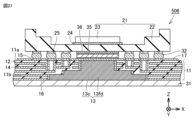
まずは図1を用いて、本実施の形態の第1例に係る放熱装置の構成上の大まかな特徴について説明する。図1は、実施の形態1の第1例に係る放熱装置の構成を示す概略断面図である。図1を参照して、本実施の形態の第1例の放熱装置101は、基板11と、実装部品21と、放熱部材31とを主に備えている。基板11は、一方の主表面である第1の主表面11aと、第1の主表面11aの反対側の他方の主表面である第2の主表面11bとを有している。図1においては第1の主表面11aは基板11のうち特に基板本体12のZ方向の最上部の表面である。図1においては第2の主表面11bは基板11のうち特に基板本体12のZ方向の最下部の表面である。実装部品21は、基板11の第1の主表面11a上に、高い熱伝導性を有する接合材料であるはんだボール32を介して載置されている。実装部品21は、駆動により熱を発する発熱部品22を含んでいる。すなわち基板11の第1の主表面11aの上方には、発熱部品22が配置されている。
Embodiment 1.
First, with reference to FIG. 1, general structural features of the heat dissipation device according to the first example of the present embodiment will be described. FIG. 1 is a schematic cross-sectional view showing the configuration of a heat dissipation device according to a first example of Embodiment 1. FIG. Referring to FIG. 1 , heat dissipation device 101 of the first example of the present embodiment mainly includes substrate 11 , mounted component 21 , and heat dissipation member 31 . The substrate 11 has a first main surface 11a, which is one main surface, and a second main surface 11b, which is the other main surface opposite to the first main surface 11a. In FIG. 1, the first main surface 11a is the uppermost surface of the substrate 11, especially the substrate body 12 in the Z direction. In FIG. 1, the second main surface 11b is the lowermost surface of the substrate 11, especially the substrate body 12 in the Z direction. Mounted component 21 is mounted on first main surface 11a of substrate 11 via solder balls 32, which are a bonding material having high thermal conductivity. Mounted component 21 includes heat-generating component 22 that generates heat when driven. That is, a heat-generating component 22 is arranged above the first main surface 11 a of the substrate 11 .

基板11は、基板本体12を主体とし、たとえば矩形の平面形状を有する板材である。すなわち基板11の基板本体12は、XY平面に沿う方向において矩形状の第1の主表面11aおよび第2の主表面11bを有し、Z方向についてある厚みを有する板材である。基板11は、熱伝導部13と、内層配線14とを含んでいる。熱伝導部13は、発熱部品22の発する熱を、たとえば図のZ方向の上側から下側へ伝える機能を有している。このため熱伝導部13はZ方向に沿って延びている。内層配線14は、基板11内にて熱伝導部13と接続されるように形成されている。ここでは内層配線14は基板11内にて熱伝導部13と熱的および電気的に接続されるように形成されている。 The substrate 11 is mainly composed of a substrate body 12 and is a plate material having, for example, a rectangular planar shape. That is, the substrate body 12 of the substrate 11 is a plate member having a rectangular first main surface 11a and a rectangular second main surface 11b in the direction along the XY plane and a certain thickness in the Z direction. The substrate 11 includes a heat conducting portion 13 and inner layer wirings 14 . The heat conducting portion 13 has a function of conducting heat generated by the heat generating component 22 from the upper side to the lower side in the Z direction of the figure, for example. Therefore, the heat conducting portion 13 extends along the Z direction. The inner layer wiring 14 is formed so as to be connected to the heat conducting portion 13 within the substrate 11 . Here, the inner layer wiring 14 is formed so as to be thermally and electrically connected to the heat conducting portion 13 within the substrate 11 .

熱伝導部13は、第1の熱伝導部13aと、第2の熱伝導部13bとを有している。第1の熱伝導部13aは、発熱部品22と平面視にて重なる領域を含んでいる。図1においては第1の熱伝導部13aは、その全体が発熱部品22と平面的に重なっている。第1の熱伝導部13aは、基板11の特に基板本体12を第1の主表面11aからその反対側の第2の主表面11bまでこれを貫通するように形成された孔部15の内部のほぼ全域を充填するように配置されている。すなわち第1の熱伝導部13aは、基板11の特に基板本体12を第1の主表面11aから第2の主表面11bまで貫通するように配置されている。第1の熱伝導部13aは、たとえば孔部15内に配置された、導電性材料からなるコアなどの構造体である。具体的には、第1の熱伝導部13aは、銅などの熱伝導率の高い材料の金属塊により形成されている。以下においてこのような金属塊をコア材と呼ぶこととする。 The heat conducting portion 13 has a first heat conducting portion 13a and a second heat conducting portion 13b. The first heat conducting portion 13a includes a region that overlaps the heat generating component 22 in plan view. In FIG. 1, the first heat conducting portion 13a is entirely overlapped with the heat generating component 22 in plan view. The first heat conducting portion 13a is formed inside a hole portion 15 formed so as to penetrate the substrate 11, particularly the substrate body 12, from the first main surface 11a to the opposite second main surface 11b. It is arranged so as to fill almost the entire area. That is, the first heat conducting portion 13a is arranged to penetrate through the substrate 11, particularly the substrate body 12, from the first main surface 11a to the second main surface 11b. The first heat conducting portion 13a is a structure such as a core made of an electrically conductive material and arranged in the hole portion 15, for example. Specifically, the first thermally conductive portion 13a is formed of a metal block of a material with high thermal conductivity such as copper. Hereinafter, such a metal lump is called a core material.

これに対し、第2の熱伝導部13bは、図のX方向またはY方向について、第1の熱伝導部13aと間隔をあけて第1の熱伝導部13aの周囲に配置されている。第2の熱伝導部13bも、基板11の特に基板本体12の内部に、たとえば図のZ方向に延びるように形成された孔部15の内部のほぼ全域を充填するように配置されている。ただし第2の熱伝導部13bは、第1の主表面11aおよび第2の主表面11bの少なくともいずれかと間隔をあけて配置されている。第2の熱伝導部13bは、たとえば孔部15内に配置された、導電性材料からなるコアなどの構造体である。具体的には、第2の熱伝導部13bは、銅などの熱伝導率の高い材料の金属塊すなわちコア材により形成されている。 On the other hand, the second heat conducting portion 13b is arranged around the first heat conducting portion 13a with a gap therebetween in the X direction or the Y direction of the figure. The second heat conducting portion 13b is also arranged inside the substrate 11, particularly inside the substrate body 12, so as to fill almost the entire inside of a hole portion 15 formed extending in the Z direction of the figure, for example. However, the second heat conducting portion 13b is spaced apart from at least one of the first main surface 11a and the second main surface 11b. The second heat conducting portion 13b is a structure such as a core made of a conductive material and arranged in the hole portion 15, for example. Specifically, the second thermally conductive portion 13b is formed of a metal lump, that is, a core material of a material having high thermal conductivity such as copper.

言い換えれば、第2の熱伝導部13bをその内部に配置する孔部15は、第1の主表面11aおよび第2の主表面11bの少なくともいずれかには露出しないように、それよりも内側に形成されている。たとえば図1においては、第2の熱伝導部13bをその内部に配置する孔部15は、第1の主表面11aには露出せず第2の主表面11bのみに露出するよう、つまり第2の主表面11bのみに通じるよう、形成されている。その結果として、図1の第2の熱伝導部13bは、第2の主表面11bに露出し、第1の主表面11aには通じず第1の主表面11aとはZ方向について間隔をあけるように配置されている。以下、図1の放熱装置101についてより詳細に説明する。 In other words, the hole portion 15 in which the second heat conducting portion 13b is arranged is arranged inside the first main surface 11a and the second main surface 11b so as not to be exposed to at least one of the first main surface 11a and the second main surface 11b. formed. For example, in FIG. 1, the hole 15 in which the second heat conducting portion 13b is arranged is exposed only to the second main surface 11b without being exposed to the first main surface 11a. is formed so as to communicate only with the main surface 11b of the . As a result, the second heat-conducting portion 13b of FIG. 1 is exposed on the second main surface 11b, does not communicate with the first main surface 11a, and is spaced apart from the first main surface 11a in the Z direction. are arranged as Hereinafter, the heat dissipation device 101 of FIG. 1 will be described in more detail.

<基板の構成>
基板11は、たとえばプリント配線基板である。基板11の基板本体12は、一般公知の樹脂材料により形成されている。後述するように基板本体12は、Z方向について図1の基板11よりも厚みが薄い板材が複数、Z方向に積層されそれらが一体となるように形成されている。この複数積層された薄い板材のそれぞれの一方または他方の主表面上には、内層配線14のパターンが形成される。内層配線14のパターンは、たとえば銅により形成された薄膜のパターンである。
<Construction of board>
Substrate 11 is, for example, a printed wiring board. A substrate body 12 of the substrate 11 is made of a generally known resin material. As will be described later, the substrate body 12 is formed by stacking a plurality of plate materials thinner in the Z direction than the substrate 11 in FIG. 1 and integrating them in the Z direction. A pattern of the inner layer wiring 14 is formed on one or the other main surface of each of the thin plate materials laminated in plurality. The pattern of inner layer wiring 14 is a pattern of a thin film made of copper, for example.

孔部15は、基板11の第1の主表面11aから第2の主表面11bまで、基板本体12を貫通するものと、Z方向について基板本体12の一部のみを延び、第1の主表面11aまたは第2の主表面11bのいずれかのみに通じるものとを有する。このうち前者の第1の主表面11aから第2の主表面11bまで基板本体12を貫通する孔部15は、図1におけるX方向の中央部に形成されており、発熱部品22と平面視にて重なる領域を含むように形成されている。図1において、このような基板本体12を貫通する孔部15は、基板本体12の中央部に1つのみ形成されている。そしてこの孔部15の内部に、第1の熱伝導部13aが挿入されている。これに対し、後者の基板本体12の一部のみを延び貫通しない孔部15は、図1において第1の熱伝導部13aの挿入される孔部15の周囲に、これとX方向およびY方向について互いに間隔をあけて複数、形成されている。図1において、複数の貫通しない孔部15のうち一部の孔部15は第1の主表面11aからZ方向下側に延びている。これらの孔部15は図1におけるZ方向の上側に形成されるため、以降においてこれを上側の非貫通の孔部15と呼ぶ。図1において、複数の貫通しない孔部15のうち他の一部の孔部15は第2の主表面11bからZ方向上側に延びている。これらの孔部15は図1におけるZ方向の下側に形成されるため、以降においてこれを下側の非貫通の孔部15と呼ぶ。 The hole portion 15 penetrates the substrate body 12 from the first main surface 11a to the second main surface 11b of the substrate 11, extends only a part of the substrate body 12 in the Z direction, and extends through the first main surface. 11a or only to the second major surface 11b. Of these, the former hole portion 15 penetrating through the substrate body 12 from the first main surface 11a to the second main surface 11b is formed in the central portion in the X direction in FIG. are formed so as to include an overlapping region. In FIG. 1 , only one hole 15 penetrating through the substrate body 12 is formed in the central portion of the substrate body 12 . A first heat conducting portion 13 a is inserted into the hole portion 15 . On the other hand, the hole portion 15 extending through only a part of the substrate body 12 and not penetrating the substrate main body 12 is arranged around the hole portion 15 into which the first heat conducting portion 13a is inserted in FIG. are formed with a plurality of spaces therebetween. In FIG. 1, some of the plurality of non-penetrating holes 15 extend downward in the Z direction from the first main surface 11a. Since these holes 15 are formed on the upper side in the Z direction in FIG. 1, they are hereinafter referred to as upper non-through holes 15 . In FIG. 1, some of the plurality of non-penetrating holes 15 extend upward in the Z direction from the second main surface 11b. Since these holes 15 are formed on the lower side in the Z direction in FIG. 1, they are hereinafter referred to as lower non-through holes 15 .

図1では、上側の非貫通の孔部15と下側の非貫通の孔部15とが平面視にて互いに重なっている。これらの複数の非貫通の孔部15は、図1においては、中央の貫通する孔部15よりもX方向の幅が細くなっている。なお図示されないが、複数の非貫通の孔部15は、中央の貫通する孔部15よりもY方向の幅が細くなっていてもよい。図1では、中央の貫通する孔部15の左側および右側に2列ずつ、非貫通の孔部15が形成されているが、この列の数は任意である。 In FIG. 1, the non-penetrating hole 15 on the upper side and the non-penetrating hole 15 on the lower side overlap each other in plan view. These non-penetrating holes 15 are narrower in width in the X direction than the central penetrating hole 15 in FIG. Although not shown, the plurality of non-penetrating holes 15 may have a smaller width in the Y direction than the penetrating hole 15 at the center. In FIG. 1, two rows of non-penetrating holes 15 are formed on the left and right sides of the central penetrating hole 15, but the number of rows is arbitrary.

これらの複数の非貫通の孔部15のうち、下側の非貫通の孔部15の内部には、第2の熱伝導部13bが挿入されている。これにより、コア材としての第2の熱伝導部13bは、第2の主表面11bに通じるように配置されている。一方図1では、複数の貫通しない孔部15のうち、上側の非貫通の孔部15の内部にはコア材としての第2の熱伝導部13bが挿入されていない。 The second heat conducting portion 13b is inserted into the lower non-penetrating hole 15 among the plurality of non-penetrating holes 15 . Thereby, the second heat conducting portion 13b as a core material is arranged so as to communicate with the second main surface 11b. On the other hand, in FIG. 1, the second heat conducting portion 13b as a core material is not inserted into the upper non-penetrating hole 15 among the plurality of non-penetrating holes 15. As shown in FIG.

つまり図1では、熱伝導部13としての第1の熱伝導部13aおよび第2の熱伝導部13bはいずれも第2の主表面11bに通じている。一方、第1の熱伝導部13aは第1の主表面11aに通じるが、第2の熱伝導部13bは第1の主表面11aに通じていない。したがって図1では、熱伝導部13としての第1の熱伝導部13aおよび第2の熱伝導部13bが第2の主表面11bに通じる部分の面積の総和は、熱伝導部13としての第1の熱伝導部13aおよび第2の熱伝導部13bが第1の主表面11aに通じる部分の面積の総和よりも大きい。 That is, in FIG. 1, both the first heat conducting portion 13a and the second heat conducting portion 13b as the heat conducting portion 13 communicate with the second main surface 11b. On the other hand, the first heat conducting portion 13a communicates with the first main surface 11a, but the second heat conducting portion 13b does not communicate with the first main surface 11a. Therefore, in FIG. 1, the sum of the areas of the portions where the first heat conducting portion 13a and the second heat conducting portion 13b as the heat conducting portion 13 communicate with the second main surface 11b is the first is larger than the total area of the portions where the heat conducting portion 13a and the second heat conducting portion 13b communicate with the first main surface 11a.

これらの複数の貫通しない孔部15のうち、下側の非貫通の孔部15の内部に挿入され当該孔部15を充填する第2の熱伝導部13bは、銅などの導電性材料からなるコア材である。これに対し、上側の非貫通の孔部15の内部には、第2の熱伝導部として、コア材としての導電性材料の代わりに、孔部15の内壁を覆う銅などの導電性部材が形成されていてもよい。この導電性部材は内壁導電膜16である。なお内壁導電膜16は、コア材としての第2の熱伝導部13bが充填される、下側の非貫通の孔部15の内壁面にも形成されていてもよい。図1においては下側の非貫通の孔部15の内壁面にも内壁導電膜16が形成されている。 Among the plurality of non-penetrating holes 15, the second heat conducting part 13b inserted into the lower non-penetrating hole 15 and filling the hole 15 is made of a conductive material such as copper. Core material. On the other hand, inside the non-penetrating hole 15 on the upper side, a conductive member such as copper covering the inner wall of the hole 15 is used as a second heat conducting member instead of the conductive material as the core material. may be formed. This conductive member is the inner wall conductive film 16 . The inner wall conductive film 16 may also be formed on the inner wall surface of the lower non-through hole 15 filled with the second heat conducting portion 13b as the core material. In FIG. 1, the inner wall conductive film 16 is also formed on the inner wall surface of the non-penetrating hole portion 15 on the lower side.

第2の熱伝導部13bは、第1の熱伝導部13aが挿入される孔部15よりもZ方向、X方向およびY方向の寸法が小さい非貫通の孔部15の内部に挿入される。このため図1では第2の熱伝導部13bは第1の熱伝導部13aよりも寸法が小さい。ただしこれに限らず、たとえば中央の貫通する孔部15の内部には、第2の熱伝導部13bとたとえば同程度に小さい第1の熱伝導部13aが複数挿入されてもよい。 The second heat conducting portion 13b is inserted into a non-penetrating hole portion 15 whose dimensions in the Z, X and Y directions are smaller than those of the hole portion 15 into which the first heat conducting portion 13a is inserted. Therefore, in FIG. 1, the second heat conducting portion 13b is smaller in size than the first heat conducting portion 13a. However, not limited to this, for example, a plurality of first heat conducting portions 13a that are approximately the same size as the second heat conducting portions 13b may be inserted into the center penetrating hole portion 15, for example.

図1においては、X方向に複数列並ぶ非貫通の孔部15のサイズは以下の特徴を有する。すなわち中央の貫通する孔部15に近づくにつれ、下側の非貫通の孔部15はZ方向に長く延び、上側の非貫通の孔部15はZ方向に短く延びている。このようにすれば、内層配線14の配置されるスペースをより多く確保できる。ただしこのような態様に限られない。内層配線14の配置スペースが確保できる限り、たとえば各列の非貫通の孔部15のうち、互いに平面視にて重なる上側の非貫通の孔部15と下側の非貫通の孔部15とがZ方向に延びる長さがほぼ等しくなっていてもよい。 In FIG. 1, the sizes of the non-penetrating holes 15 arranged in a plurality of rows in the X direction have the following characteristics. That is, the lower non-through hole 15 extends longer in the Z direction, and the upper non-through hole 15 extends shorter in the Z direction as the central through hole 15 is approached. In this way, more space for arranging the inner layer wiring 14 can be secured. However, it is not limited to such a mode. As long as a space for arranging the inner layer wiring 14 can be secured, for example, among the non-penetrating holes 15 in each row, the upper non-penetrating hole 15 and the lower non-penetrating hole 15 that overlap each other in plan view are The lengths extending in the Z direction may be substantially equal.

また図1に示すように、第2の主表面11b側に通じる熱伝導部13のコア材の総数が、第1の主表面11a側に通じる熱伝導部13のコア材の総数よりも大きくてもよい。具体的には図1においては、第1の主表面11aに通じるコア材は1つの第1の熱伝導部13aのみである。これに対し図1においては、第2の主表面11bに通じるコア材は1つの第1の熱伝導部13aと4つの第2の熱伝導部13bとの合計5つである。 Further, as shown in FIG. 1, the total number of core materials of the heat conducting portion 13 leading to the second main surface 11b side is larger than the total number of core members of the heat conducting portion 13 leading to the first main surface 11a side. good too. Specifically, in FIG. 1, the core material communicating with the first main surface 11a is only one first heat conducting portion 13a. On the other hand, in FIG. 1, there are a total of five core members communicating with the second main surface 11b, one first heat conducting portion 13a and four second heat conducting portions 13b.

図1において、内層配線14は、第1の熱伝導部13aと第2の熱伝導部13bとを接続するように配置されている。ここでは内層配線14は、第1の熱伝導部13aと第2の熱伝導部13bとを熱的および電気的に接続することを意味している。 In FIG. 1, the inner layer wiring 14 is arranged so as to connect the first heat conducting portion 13a and the second heat conducting portion 13b. Here, the inner layer wiring 14 means to thermally and electrically connect the first heat conducting portion 13a and the second heat conducting portion 13b.

具体的には、たとえば基板11に形成された孔部15内に、コア材としての第1の熱伝導部13aと、コア材としての第2の熱伝導部13bとが、充填されている。これらの孔部15は後述するように、樹脂製の基板本体12とその上に形成された内層配線14となるべき銅などの薄膜パターンの部分にそれらが欠落した部分として形成されたものである。このため孔部15の内壁面の少なくとも一部には内層配線14が露出している。この孔部15内にコア材としての導体材料の熱伝導部13が挿入される。熱伝導部13の表面の少なくとも一部が、孔部15の内壁面を形成する内層配線14の露出部に接触する。これにより、孔部15内の熱伝導部13と、孔部15の内壁面に露出する内層配線14とが接触した部分にて、第1の熱伝導部13aと第2の熱伝導部13bとが、内層配線14と接続される。これらの接続は、熱的および電気的になされる。 Specifically, for example, a hole portion 15 formed in the substrate 11 is filled with a first heat conducting portion 13a as a core material and a second heat conducting portion 13b as a core material. As will be described later, these holes 15 are formed as portions missing from the resin-made substrate body 12 and thin-film pattern portions of copper or the like that are to become the inner layer wirings 14 formed thereon. . Therefore, the inner layer wiring 14 is exposed on at least a part of the inner wall surface of the hole 15 . A heat conducting portion 13 made of a conductive material as a core material is inserted into the hole portion 15 . At least part of the surface of the heat conducting portion 13 contacts the exposed portion of the inner layer wiring 14 forming the inner wall surface of the hole portion 15 . As a result, the first heat conducting portion 13a and the second heat conducting portion 13b are formed at the portion where the heat conducting portion 13 in the hole portion 15 and the inner layer wiring 14 exposed on the inner wall surface of the hole portion 15 are in contact with each other. is connected to the inner layer wiring 14 . These connections are made thermally and electrically.

ただし孔部15内の熱伝導部13と内層配線14とは、これらの間にたとえば内壁面のめっき膜としての内壁導電膜16などの他の導電性部材または薄い樹脂等を挟むように接続される場合もある。この場合においても、熱伝導部13と内層配線14とはこれらの間の内壁導電膜16および薄い樹脂などの部材を介して少なくとも熱的に接続される。つまり熱伝導部13と内層配線14との間の熱の伝導が可能である。そこで本実施の形態では、このような場合も含めて熱伝導部13すなわち第1の熱伝導部13aおよび第2の熱伝導部13bと内層配線14とが「接続されている」ものと定義する。また第1の熱伝導部13aが挿入される孔部15内の内壁導電膜16および第2の熱伝導部13bが挿入される孔部15内の内壁導電膜16を介して、第1の熱伝導部13aと第2の熱伝導部13bとが少なくとも熱的に接続される。このため内層配線14は、たとえば内壁導電膜16を介して、第1の熱伝導部13aと第2の熱伝導部13bとを接続するように、すなわち少なくとも熱的に接続するように、配置される。ただし熱伝導部13と内層配線14とはたとえば内壁導電膜16を介して電気的に接続されることがより好ましい。また内層配線14は第1の熱伝導部13aと第2の熱伝導部13bとを内壁導電膜16を介して電気的に接続されることがより好ましい。 However, the heat conducting portion 13 in the hole portion 15 and the inner layer wiring 14 are connected so as to sandwich another conductive member such as an inner wall conductive film 16 as a plated film on the inner wall surface or a thin resin or the like between them. sometimes Also in this case, the heat conducting portion 13 and the inner layer wiring 14 are at least thermally connected via the inner wall conductive film 16 and a member such as a thin resin between them. That is, heat can be conducted between the heat conducting portion 13 and the inner layer wiring 14 . Therefore, in the present embodiment, the heat conducting portion 13, that is, the first heat conducting portion 13a and the second heat conducting portion 13b and the inner layer wiring 14 are defined to be "connected" including such a case. . In addition, the first heat is transmitted via the inner wall conductive film 16 in the hole 15 into which the first heat conducting portion 13a is inserted and the inner wall conductive film 16 in the hole 15 into which the second heat conducting portion 13b is inserted. Conducting portion 13a and second heat conducting portion 13b are at least thermally connected. For this reason, the inner layer wiring 14 is arranged to connect the first heat conducting portion 13a and the second heat conducting portion 13b via the inner wall conductive film 16, that is, to at least thermally connect them. be. However, it is more preferable that the heat conducting portion 13 and the inner layer wiring 14 are electrically connected via the inner wall conductive film 16, for example. More preferably, the inner layer wiring 14 electrically connects the first heat conducting portion 13 a and the second heat conducting portion 13 b via the inner wall conductive film 16 .

なお基板11にはZ方向に互いに間隔をあけて複数層の内層配線14が形成されている。ただし基板11の第1の主表面11a上には、表層配線17が形成されている。この表層配線17のパターンは、内層配線14のパターンと同一の材質および厚みにより形成されている。すなわち表層配線17は、たとえば銅により形成された薄膜のパターンである。なお上側の非貫通の孔部15の直上には、表層配線17とたとえば同一の材質および厚みであるめっき膜17aが形成されている。めっき膜17aはたとえばめっきにより形成された銅の薄膜である。めっき膜17aは孔部15の形成により除去された内層配線14の部分を補うように形成される導電膜である。したがってめっき膜17aは、孔部15をZ方向の上側から塞ぐように形成されている。 A plurality of inner layer wirings 14 are formed on the substrate 11 at intervals in the Z direction. However, a surface layer wiring 17 is formed on the first main surface 11 a of the substrate 11 . The pattern of the surface layer wiring 17 is formed of the same material and thickness as the pattern of the inner layer wiring 14 . That is, surface wiring 17 is a pattern of a thin film made of copper, for example. A plated film 17a having the same material and thickness as surface wiring 17, for example, is formed directly above non-penetrating hole 15 on the upper side. Plated film 17a is, for example, a copper thin film formed by plating. The plating film 17a is a conductive film formed so as to compensate for the portion of the inner layer wiring 14 removed by forming the hole 15. As shown in FIG. Therefore, the plated film 17a is formed so as to close the hole 15 from above in the Z direction.

<実装部品の構成>
実装部品21は、発熱部品22と、パッケージ23とを含んでいる。発熱部品22は、たとえばシリコン(Si)、ガリウム窒素またはガリウムヒ素の基板に形成された半導体トランジスタまたはダイオードを有する半導体素子である。発熱部品22は、上記半導体素子の駆動により発熱する。パッケージ23は、単層または多層の樹脂基板またはセラミック基板により形成されるケース状の部材である。ただしパッケージ23は金属製のケース状の部材であってもよい。パッケージ23は発熱部品22を内部に収納する。パッケージ23はたとえば、ガルウイングパッケージ、フラットリードパッケージ、QFN(Quad For Non-Lead)パッケージ、BGA(Ball Grid Array)パッケージからなる群から選択されるいずれかであることが好ましい。発熱部品22は、パッケージ23の内部のたとえば底面上に、はんだなどの接合層24により接合されている。
<Configuration of mounted parts>
Mounted component 21 includes heat-generating component 22 and package 23 . Heat-generating component 22 is a semiconductor element having a semiconductor transistor or diode formed on a substrate of silicon (Si), gallium nitrogen, or gallium arsenide, for example. The heat-generating component 22 generates heat by driving the semiconductor element. The package 23 is a case-shaped member formed of a single-layer or multi-layer resin substrate or ceramic substrate. However, the package 23 may be a metal case-like member. The package 23 accommodates the heat-generating component 22 inside. The package 23 is preferably one selected from the group consisting of, for example, a gull wing package, a flat lead package, a QFN (Quad For Non-Lead) package, and a BGA (Ball Grid Array) package. The heat-generating component 22 is bonded to, for example, the bottom surface inside the package 23 with a bonding layer 24 such as solder.

<その他の部材>
基板11の第2の主表面11b上の表層配線17に接するように、基板11には放熱部材31が接合されている。つまり基板11の、発熱部品22を含む実装部品21が実装される第1の主表面11a側と反対側である第2の主表面11b側には、放熱部材31が接合されている。放熱部材31は一般公知のたとえば銅製のヒートシンクなどである。ただしこれに限らず、放熱部材31として他の冷却器が用いられてもよい。
<Other parts>
A heat dissipation member 31 is joined to the substrate 11 so as to be in contact with the surface wiring 17 on the second main surface 11 b of the substrate 11 . That is, the heat radiating member 31 is bonded to the second main surface 11b side of the substrate 11, which is opposite to the first main surface 11a side on which the mounting component 21 including the heat generating component 22 is mounted. The heat dissipation member 31 is a generally known heat sink made of copper, for example. However, not limited to this, another cooler may be used as the heat dissipation member 31 .

基板11の第1の主表面11a上の表層配線17およびめっき膜17aに接するように、はんだボール32が複数、互いに間隔をあけて配置されている。これらのはんだボール32は、パッケージ23の最下面に形成された導電膜のパターンに接するように配置されている。パッケージ23の当該導電膜のパターンは、発熱部品22に含まれる半導体素子と電気的に接続されていることが好ましい。これによりはんだボール32は、基板11と実装部品21とを電気的に接続している。 A plurality of solder balls 32 are spaced apart from each other so as to be in contact with surface wiring 17 and plating film 17a on first main surface 11a of substrate 11 . These solder balls 32 are arranged so as to be in contact with the conductive film pattern formed on the bottom surface of the package 23 . It is preferable that the pattern of the conductive film of the package 23 is electrically connected to the semiconductor element included in the heat-generating component 22 . Accordingly, the solder balls 32 electrically connect the board 11 and the mounted component 21 .

本実施の形態でのはんだボール32は、たとえば金属コアを含むはんだ材料、または銀ペーストのような、熱伝導性が高くリフロー可能な接合材料であることが好ましい。これによりはんだボール32は、基板11と実装部品21とを低熱抵抗で接続できる。 The solder balls 32 in this embodiment are preferably a solder material containing a metal core, or a bonding material that is highly thermally conductive and reflowable, such as silver paste. As a result, the solder balls 32 can connect the board 11 and the mounting component 21 with low thermal resistance.

<放熱装置の動作>
以上の構成を有する放熱装置101は以下のように動作する。半導体素子の駆動により発熱部品22で発生した熱は、パッケージ23とはんだボール32とを介して、基板11の、発熱部品22と平面的に重なる第1の熱伝導部13aに伝熱される。第1の熱伝導部13aは、その真下の放熱部材31側へと放熱することができる。また第1の熱伝導部13aは、これが配置される孔部15の内壁面の内壁導電膜16を介して、あるいは直接、内層配線14に接続されている。また第2の熱伝導部13bも同様に、これが配置される孔部15の内壁面の内壁導電膜16を介して、あるいは直接、内層配線14に接続されている。つまり第1の熱伝導部13aは、内層配線14を介して、第2の熱伝導部13bに、少なくとも熱的に接続されている。このため第1の熱伝導部13aに伝わった熱は、内層配線14を介して第2の熱伝導部13bに伝わることができる。第2の熱伝導部13bは第1の熱伝導部13aと同様に、その真下の放熱部材31側へと放熱することができる。
<Operation of heat sink>
The heat dissipation device 101 having the above configuration operates as follows. The heat generated by the heat-generating component 22 due to the driving of the semiconductor element is transferred to the first heat-conducting portion 13a of the substrate 11, which planarly overlaps the heat-generating component 22, via the package 23 and the solder balls 32. The first heat conducting portion 13a can dissipate heat toward the heat dissipating member 31 directly below. Also, the first heat conducting portion 13a is connected to the inner layer wiring 14 via the inner wall conductive film 16 on the inner wall surface of the hole portion 15 in which the first heat conducting portion 13a is arranged, or directly. Similarly, the second heat conducting portion 13b is also connected to the inner layer wiring 14 via the inner wall conductive film 16 on the inner wall surface of the hole portion 15 in which it is arranged, or directly. That is, the first thermally conductive portion 13a is at least thermally connected to the second thermally conductive portion 13b through the inner layer wiring 14 . Therefore, the heat transmitted to the first heat conductive portion 13a can be transmitted to the second heat conductive portion 13b via the inner layer wiring 14. As shown in FIG. Like the first heat conducting portion 13a, the second heat conducting portion 13b can dissipate heat toward the heat dissipating member 31 directly below.

図2は、実施の形態1の第2例に係る放熱装置の構成を示す概略断面図である。なお以降の各図において、図1と同一の構成要素には同一の符号を付し、図1と同様の構成および特徴についてはその説明を繰り返さない。すなわち以降の各例の説明においては、図1または既存の他例と異なる構成および特徴を中心に説明する。図2を参照して、本実施の形態の第2例の放熱装置102においては、基板本体12を貫通する孔部15は、基板本体12の中央部に、互いに間隔をあけて複数、形成されている。図2においては1例として3つの貫通する孔部15が示されるが、孔部15の数はこれに限られない。そしてこれらの孔部15の内部に、第1の熱伝導部13aが挿入されている。このため図2における個々の第1の熱伝導部13aは、図1における個々の第1の熱伝導部13aよりも、X方向およびY方向の寸法が小さい。 FIG. 2 is a schematic cross-sectional view showing the configuration of a heat dissipation device according to a second example of the first embodiment. In each of the subsequent figures, the same components as in FIG. 1 are denoted by the same reference numerals, and the same configurations and features as in FIG. 1 will not be described repeatedly. That is, in the description of each example below, the description will focus on the configuration and features that are different from those of FIG. 1 or other existing examples. Referring to FIG. 2, in heat dissipation device 102 of the second example of the present embodiment, a plurality of holes 15 penetrating substrate body 12 are formed in the central portion of substrate body 12 at intervals. ing. Although three penetrating holes 15 are shown in FIG. 2 as an example, the number of holes 15 is not limited to this. A first heat conducting portion 13 a is inserted into these holes 15 . For this reason, the individual first heat conducting portions 13a in FIG. 2 have smaller dimensions in the X direction and the Y direction than the individual first heat conducting portions 13a in FIG.

図3は、実施の形態1の第3例に係る放熱装置の構成を示す概略断面図である。図3を参照して、本実施の形態の第3例の放熱装置103においては、最も中央の貫通された孔部15に近い上側の非貫通の孔部15は、上記他例と同様、これと平面視にて重なるように、下側の非貫通の孔部15を有する。当該下側の非貫通の孔部15は第2の熱伝導部13bにより充填されている。ただしその外側の上側の非貫通の孔部15は、平面視にて下側の非貫通の孔部15と重なっていない。そして当該上側の非貫通の孔部15のさらに外側に、下側の非貫通の孔部15を有している。この下側の非貫通の孔部15の内部には第2の熱伝導部13bが充填されていない。当該外側の上側の非貫通の孔部15と、下側の非貫通の孔部15とは、内層配線14により繋がっている。 FIG. 3 is a schematic cross-sectional view showing the configuration of a heat dissipation device according to a third example of the first embodiment. Referring to FIG. 3, in heat dissipation device 103 of the third example of the present embodiment, upper non-penetrating hole 15 closest to central penetrating hole 15 is similar to the other examples above. It has a lower non-penetrating hole 15 so as to overlap with the bottom when viewed from the top. The lower non-penetrating hole portion 15 is filled with the second heat conducting portion 13b. However, the non-through hole 15 on the outer side does not overlap with the non-through hole 15 on the lower side in plan view. Further outside the upper non-penetrating hole 15 , there is a lower non-penetrating hole 15 . The inside of the non-penetrating hole 15 on the lower side is not filled with the second heat conducting portion 13b. The upper non-penetrating hole 15 and the lower non-penetrating hole 15 of the outside are connected by an inner layer wiring 14 .

また放熱装置103においては、基板11と放熱部材31との間に、非導電放熱シート33が配置されている。非導電放熱シート33には、高い熱伝導性を持つ絶縁材料としてエポキシ樹脂などが用いられる。非導電放熱シート33は平板形状の部材である。これが基板11の第2の主表面11b側であり放熱部材31のZ方向上側に接合されている。 Moreover, in the heat dissipation device 103 , a non-conductive heat dissipation sheet 33 is arranged between the substrate 11 and the heat dissipation member 31 . Epoxy resin or the like is used as an insulating material having high thermal conductivity for the non-conductive heat dissipation sheet 33 . The non-conductive heat radiation sheet 33 is a plate-shaped member. This is the second main surface 11b side of the substrate 11 and is joined to the upper side of the heat dissipation member 31 in the Z direction.

上側の非貫通の孔部15は、フレームグランドとしても機能する放熱部材31への接続を避けたい場合がある。しかしその目的のために孔部15を非貫通とすれば、その孔部15は第2の主表面11bに達しないため放熱性に劣る。そこで図3のように非導電放熱シート33が基板11と放熱部材31との間に配置される。これにより図3のように、上側の非貫通の孔部15と、下側の非貫通の孔部15とを内層配線14などにより電気的に接続し、これらが一体となったものが得られる。これらが一体となったものが、実装部品21から下方の放熱部材31側への放熱を可能とするため、放熱装置103全体の放熱機能が高められる。 It may be desirable to avoid connecting the upper non-through hole 15 to the heat dissipation member 31 that also functions as a frame ground. However, if the hole 15 is made non-penetrating for that purpose, the hole 15 does not reach the second main surface 11b, resulting in poor heat dissipation. Therefore, a non-conductive heat radiation sheet 33 is arranged between the substrate 11 and the heat radiation member 31 as shown in FIG. As a result, as shown in FIG. 3, the non-penetrating hole 15 on the upper side and the non-penetrating hole 15 on the lower side are electrically connected to each other by the inner layer wiring 14 or the like, and an integrated structure is obtained. . The combination of these elements enables heat dissipation from the mounting component 21 to the lower heat dissipation member 31 side, so that the heat dissipation function of the heat dissipation device 103 as a whole is enhanced.

次に、図4のフローチャートを用いて、図1または図2の放熱装置101,102,103を構成する、特に基板11の製造工程について説明する。なお放熱装置101~103の間では孔部15の位置等が異なるが、以下では全例に共通のプロセスについて説明する。図4は、実施の形態1の各例の放熱装置に含まれる基板の製造工程を示すフローチャートである。図4を参照して、まず準備工程(S10)がなされる。具体的には、樹脂製の薄い、基板本体12となるべき矩形状の板材が複数準備される。この複数の板材のそれぞれの一方または双方の主表面上に、たとえば銅の配線パターンが形成される。その後、当該複数の板材のそれぞれにこれを一方の主表面からその反対側の他方の主表面まで貫通するビアが形成される。このビアは、たとえば複数の板材のうち一の板材と他の板材とが重ね合わせられたときに、一の板材のビアと他の板材のビアとが同位置にて重なりあうように形成されることが好ましい。特に複数の板材が重ね合わせられたときに、上記ビア同士が重なり合うことにより、それらのビアが図1~図3のいずれかの基板11の非貫通の孔部15を形成する態様であることが好ましい。またビアの内壁面には、たとえばめっき工程により銅の薄膜が、内壁導電膜16となるべき膜として形成される。 Next, a manufacturing process of particularly the substrate 11, which constitutes the heat dissipation devices 101, 102, and 103 of FIG. 1 or 2, will be described with reference to the flow chart of FIG. Although the positions of the holes 15 and the like are different between the radiators 101 to 103, processes common to all examples will be described below. 4 is a flow chart showing a manufacturing process of a substrate included in each example of the heat dissipation device of Embodiment 1. FIG. Referring to FIG. 4, first, a preparation step (S10) is performed. Specifically, a plurality of thin rectangular plate members made of resin to be the substrate body 12 are prepared. A copper wiring pattern, for example, is formed on one or both main surfaces of each of the plurality of plate members. After that, vias are formed through each of the plurality of plate members from one main surface to the other main surface on the opposite side. The vias are formed such that, for example, when one of a plurality of plate materials is superimposed on another plate material, the via of one plate material and the via of the other plate material overlap at the same position. is preferred. In particular, when a plurality of plate materials are superimposed, the vias overlap each other, and the vias form the non-penetrating holes 15 of the substrate 11 shown in any one of FIGS. 1 to 3. preferable. On the inner wall surface of the via, for example, a copper thin film is formed as a film to become the inner wall conductive film 16 by a plating process.

次に積層工程(S20)がなされる。プリプレグと呼ばれるシートが、当該各板材の上に重ねられた状態で、当該各板材が重ね合わせられる。そして接着工程(S30)がなされる。重ね合わせられた複数の板材が、高温高圧下にさらされる。これにより、プリプレグが当該複数の板材同士を接着する。このとき、ビア同士の接続により非貫通の孔部15が形成される。以上の工程(S20)および(S30)が、必要な基板11のZ方向の厚みとなるまで複数回、繰り返されてもよい。 Next, a stacking step (S20) is performed. A sheet called prepreg is superimposed on each of the plate members, and the plate members are superimposed on each other. Then, a bonding step (S30) is performed. A plurality of stacked plate materials are exposed to high temperature and high pressure. As a result, the prepreg bonds the plurality of plate members together. At this time, non-penetrating holes 15 are formed by connecting vias. The above steps (S20) and (S30) may be repeated multiple times until the required thickness of the substrate 11 in the Z direction is obtained.

必要な厚みの基板11が形成されたところで、穴あけ加工工程(S40)として、基板本体12全体の第1の主表面11aから第2の主表面11bまでこれを貫通するように、基板11を貫通する孔部15が形成される。またこの孔部15の内壁面にも、たとえばめっき工程により銅の薄膜が、内壁導電膜16として形成されてもよい。 When the substrate 11 having the required thickness is formed, in the drilling step (S40), the substrate 11 is penetrated from the first main surface 11a of the entire substrate body 12 to the second main surface 11b. A hole portion 15 is formed. A copper thin film may also be formed as the inner wall conductive film 16 on the inner wall surface of the hole 15 by, for example, a plating process.

その後、基板11の全体を貫通する孔部15には第1の熱伝導部13aのコア材が、たとえば圧入工程により挿入される。コア材は孔部15のほぼ全体を充填する。コア材の少なくとも一部が、孔部15の内壁面として露出する内層配線14、またはその内壁面を覆う内壁導電膜16の部分に接触する。また同様に、基板11を貫通しない孔部15のうち、特に第2の主表面11bに通じるように形成された孔部15内には、第2の熱伝導部13bのコア材が、たとえば圧入工程により挿入される。第1の熱伝導部13aおよび第2の熱伝導部13bは、あらかじめ金属塊となるように整形されたコア材である。コア材が挿入された後、必要に応じて熱処理工程および化学工程がなされてもよい。 After that, the core material of the first heat conducting portion 13a is inserted into the hole portion 15 penetrating the entire substrate 11 by, for example, a press-fitting process. The core material fills substantially the entire hole 15 . At least part of the core material contacts the inner layer wiring 14 exposed as the inner wall surface of the hole 15 or the inner wall conductive film 16 covering the inner wall surface. Similarly, among the holes 15 that do not penetrate the substrate 11, the core material of the second heat conducting portion 13b is press-fitted, for example, into the holes 15 that are formed to communicate with the second main surface 11b. inserted by the process. The first heat-conducting portion 13a and the second heat-conducting portion 13b are core materials preliminarily shaped into metal lumps. After the core material is inserted, heat treatment and chemical steps may be performed as required.

その後、必要に応じて、基板本体12の孔部15の内壁面と、その内部に充填された熱伝導部13のコア材との隙間に穴埋め樹脂が充填されてもよい。あるいは圧入工程により孔部15内に挿入された熱伝導部13が部分的にかしめられてもよい。そのようにすれば熱伝導部13は樹脂材料を介在することなく孔部15内に固定される。 After that, if necessary, the gap between the inner wall surface of the hole portion 15 of the substrate body 12 and the core material of the heat conducting portion 13 filled therein may be filled with a filling resin. Alternatively, the heat-conducting portion 13 inserted into the hole portion 15 by a press-fitting process may be partially crimped. By doing so, the heat conducting portion 13 is fixed in the hole portion 15 without interposing the resin material.

次に、本実施の形態の作用効果について説明する。 Next, the effects of this embodiment will be described.

本開示に従った放熱装置は、基板11と、発熱部品22とを備える。発熱部品22は基板11の第1の主表面11aの上に配置されている。基板11は、熱伝導部13と、内層配線14とを含む。熱伝導部13は、発熱部品22の発する熱を伝える。内層配線14は、基板11内にて熱伝導部13と接続されるように形成されている。熱伝導部13は、第1の熱伝導部13aと、第2の熱伝導部13bとを有する。第1の熱伝導部13aは、発熱部品22と平面視にて重なる領域を含み、第1の主表面11aから第1の主表面11aと反対側の第2の主表面11bまで基板11を貫通する。第2の熱伝導部13bは、第1の熱伝導部13aと間隔をあけて第1の熱伝導部13aの周囲に配置され、第1の主表面11aおよび第2の主表面11bの少なくともいずれかと間隔をあけて配置される。 A heat dissipation device according to the present disclosure comprises a substrate 11 and a heat generating component 22 . Heat-generating component 22 is arranged on first main surface 11 a of substrate 11 . The substrate 11 includes a heat conducting portion 13 and inner layer wirings 14 . The heat conducting portion 13 conducts heat generated by the heat generating component 22 . The inner layer wiring 14 is formed so as to be connected to the heat conducting portion 13 within the substrate 11 . The heat conducting portion 13 has a first heat conducting portion 13a and a second heat conducting portion 13b. The first heat conducting portion 13a includes a region that overlaps with the heat generating component 22 in a plan view, and penetrates the substrate 11 from the first main surface 11a to the second main surface 11b opposite to the first main surface 11a. do. The second heat-conducting portion 13b is arranged around the first heat-conducting portion 13a with a gap from the first heat-conducting portion 13a. are placed with a gap between them.

発熱部品22と平面視にて重なる領域を含む第1の熱伝導部13aには、発熱部品22の熱が直接伝わる。熱伝導部13と内層配線14とは接続、特に熱的に接続されるように配置されている。このため第1の熱伝導部13aに伝わった熱は、内層配線14に伝わり、そこから第2の熱伝導部13bに容易に伝えらえる。これにより、発熱部品22の熱を第1の熱伝導部13aのみならずその周囲の第2の熱伝導部13bにも分散することができる。このため第1の熱伝導部13aと第2の熱伝導部13bとから放熱装置101などの外部へ放熱することができる。すなわちたとえば第1の熱伝導部13aのみを有する場合に比べて放熱ルートの熱抵抗を低下させることができる。その結果、放熱装置101~103全体で高い放熱性能を実現できる。 The heat of the heat-generating component 22 is directly transmitted to the first heat conducting portion 13a including a region that overlaps with the heat-generating component 22 in plan view. The heat conducting portion 13 and the inner layer wiring 14 are arranged so as to be connected, particularly thermally connected. Therefore, the heat transmitted to the first heat conductive portion 13a is transmitted to the inner layer wiring 14, and is easily transmitted from there to the second heat conductive portion 13b. Thereby, the heat of the heat-generating component 22 can be dispersed not only in the first heat-conducting portion 13a but also in the surrounding second heat-conducting portion 13b. Therefore, the heat can be radiated to the outside such as the heat dissipation device 101 from the first heat conducting portion 13a and the second heat conducting portion 13b. That is, the thermal resistance of the heat dissipation route can be reduced compared to the case where only the first heat conducting portion 13a is provided, for example. As a result, the heat dissipation devices 101 to 103 as a whole can achieve high heat dissipation performance.

発熱部品22の熱はその真下の第1の熱伝導部13aに高い放熱性で伝わる。しかし仮にそこから真下の放熱部材31に伝熱するルートのみが存在すれば、なお放熱機能が不十分となる可能性がある。そこで第1の熱伝導部13aと熱的に接続された内層配線14を介し、第1の熱伝導部13aから第2の熱伝導部13bに熱を伝えるルートを追加で配置している。このため放熱装置101~103においては発熱部品22から放熱部材31への放熱ルートが増加し、いっそう高い放熱性能が実現できる。 The heat of the heat-generating component 22 is transferred to the first heat-conducting portion 13a directly below it with high heat dissipation. However, if there were only a route for transferring heat from there to the heat dissipating member 31 directly below, there is a possibility that the heat dissipating function would still be insufficient. Therefore, a route for conducting heat from the first heat conducting portion 13a to the second heat conducting portion 13b is additionally arranged via the inner layer wiring 14 thermally connected to the first heat conducting portion 13a. Therefore, in the heat dissipation devices 101 to 103, the number of heat dissipation routes from the heat generating component 22 to the heat dissipation member 31 is increased, and a higher heat dissipation performance can be realized.

第2の熱伝導部13bは、たとえば第1の主表面11aと間隔をあけて配置される。逆に言えば第2の熱伝導部13bは、たとえば第2の主表面11b側に配置される。これにより、特に基板11のうち発熱部品22が配置される第1の主表面11a側と反対側の第2の主表面11b側にて、第2の熱伝導部13bによる放熱部材31側への放熱機能をより高めることができる。 Second heat conducting portion 13b is arranged, for example, with a gap from first main surface 11a. Conversely, second heat conducting portion 13b is arranged, for example, on the second main surface 11b side. As a result, particularly on the second main surface 11b side of the substrate 11 opposite to the first main surface 11a side where the heat generating component 22 is arranged, the second heat conducting portion 13b allows the heat dissipation member 31 side to pass through. The heat dissipation function can be further enhanced.

また第2の熱伝導部13bは、たとえば第1の主表面11aと間隔をあけて配置される。このため基板11内の特に第1の主表面11aに近い領域には、実装部品21の電源および制御信号を引き回すためのスペースを増加できる。なお基板11内にて第1の熱伝導部13aの周囲に配置されるべき実装部品21の電源および制御信号の数量は、第1の熱伝導部13aの周囲に配置される実装部品21の電源および制御信号により制約される。基板11内の特に第1の主表面11aに近い領域を電源および制御信号の配置領域とする。これにより、基板11内の特に発熱部品22が配置される側と反対側である第2の主表面11bに近い領域を、第2の熱伝導部13bを配置し、発熱部品22の熱を第2の熱伝導部13bから放熱装置の外部へ放出する領域とできる。 Second heat conducting portion 13b is arranged, for example, with a gap from first main surface 11a. Therefore, the space for routing the power supply and control signals of the mounted component 21 can be increased in the region within the substrate 11, particularly near the first main surface 11a. Note that the number of power sources and control signals for the mounted components 21 to be arranged around the first heat conducting portion 13a in the substrate 11 is and control signals. A region in the substrate 11 that is particularly close to the first main surface 11a is used as a power supply and control signal arrangement region. As a result, the second heat conducting portion 13b is arranged in the area near the second main surface 11b, which is the side opposite to the side on which the heat-generating component 22 is arranged, in the substrate 11 in particular, so that the heat of the heat-generating component 22 is transferred to the second main surface 11b. 2 from the heat conducting portion 13b to the outside of the heat dissipation device.

以上の効果を奏する観点から、上記放熱装置において、第2の熱伝導部13bは、第2の主表面11bに通じるように配置されていることが好ましい。上記放熱装置において、熱伝導部13としての第1の熱伝導部13aおよび第2の熱伝導部13bが第2の主表面11bに通じる部分の面積の総和は、熱伝導部13としての第1の熱伝導部13aおよび第2の熱伝導部13bが第1の主表面11aに通じる部分の面積の総和より大きいことが好ましい。このようにすれば、熱伝導部13が基板11の第2の主表面11b上にて第1の主表面11a上よりも広い面積にて、あるいは多数、配置される。このため、第2の主表面11b側にてより効率的に、発熱部品22の熱を放熱部材31から基板11の外部に放熱できる。 From the viewpoint of achieving the above effects, in the heat dissipation device, it is preferable that the second heat conducting portion 13b is arranged so as to communicate with the second main surface 11b. In the above heat dissipation device, the total area of the portions where the first heat conducting portion 13a and the second heat conducting portion 13b as the heat conducting portion 13 communicate with the second main surface 11b is It is preferable that the heat conducting portion 13a and the second heat conducting portion 13b are larger than the total area of the portions communicating with the first main surface 11a. In this way, the heat conducting portions 13 are arranged on the second main surface 11b of the substrate 11 in a larger area than on the first main surface 11a, or in a large number. Therefore, the heat of the heat-generating component 22 can be more efficiently radiated to the outside of the substrate 11 from the heat radiating member 31 on the second main surface 11b side.

上記放熱装置において、第2の熱伝導部13bは、基板11に形成された孔部15内に充填された導電性部材としてのコア材により形成されることが好ましい。このようにすれば、第2の熱伝導部13bによる放熱機能をいっそう高めることができる。 In the heat dissipation device described above, the second heat conducting portion 13 b is preferably formed of a core material as a conductive member filled in the hole 15 formed in the substrate 11 . By doing so, the heat dissipation function of the second heat conducting portion 13b can be further enhanced.

ただし上記放熱装置において、第2の熱伝導部は、基板11に形成された孔部15の内壁を覆う導電性部材としての内壁導電膜16により形成されてもよい。この場合、孔部15内の内壁導電膜16の内側にはコア材などが配置されず、空洞となっている。しかしこの場合においても、内壁導電膜16の熱伝導性により、第2の熱伝導部の最低限の熱伝導性を確保できる。コア材を設けないため、このような第2の熱伝導部は、材料費の削減により製造コストを削減できる。 However, in the heat dissipation device described above, the second heat conducting portion may be formed of an inner wall conductive film 16 as a conductive member covering the inner wall of the hole 15 formed in the substrate 11 . In this case, a core material or the like is not arranged inside the inner wall conductive film 16 in the hole 15, and a cavity is formed. However, even in this case, the thermal conductivity of the inner wall conductive film 16 ensures the minimum thermal conductivity of the second thermally conductive portion. Since the core material is not provided, such a second heat conducting part can reduce the manufacturing cost by reducing the material cost.

上記放熱装置において、内層配線14は、第1の熱伝導部13aと第2の熱伝導部13bとを接続するように配置されることが好ましい。たとえば基板本体12を構成する樹脂材料は、発熱部品22からその真下の第1の熱伝導部13aに伝わった熱を第2の熱伝導部13bに十分に伝えることが困難である。そこで第1の熱伝導部13aと第2の熱伝導部13bとを内層配線14で接続する。これにより、第1の熱伝導部13aの熱を、内層配線14を介して、第2の熱伝導部13bに容易に伝えることができる。このようにすれば、発熱部品22の熱は、第1の熱伝導部13aのみならず、第2の熱伝導部13bからも、外部に放熱できる。 In the heat dissipation device described above, the inner layer wiring 14 is preferably arranged to connect the first heat conducting portion 13a and the second heat conducting portion 13b. For example, it is difficult for the resin material forming the substrate body 12 to sufficiently transfer the heat transferred from the heat-generating component 22 to the first heat-conducting portion 13a immediately below it to the second heat-conducting portion 13b. Therefore, the first heat conducting portion 13 a and the second heat conducting portion 13 b are connected by the inner layer wiring 14 . Thereby, the heat of the first thermally conductive portion 13a can be easily transferred to the second thermally conductive portion 13b through the inner layer wiring 14 . In this way, the heat of the heat-generating component 22 can be radiated to the outside not only from the first heat-conducting portion 13a but also from the second heat-conducting portion 13b.

実施の形態2.
図5は、実施の形態2に係る放熱装置の構成を示す概略断面図である。図5を参照して、本実施の形態においては、第3の熱伝導部13cを有している。具体的には、図5の実施の形態2の放熱装置201においては、発熱部品22と第1の熱伝導部13aとの間に、熱伝導部13としての第3の熱伝導部13cが挟まれるように配置されている。第3の熱伝導部13cは発熱部品22と平面視にて重なる領域を含むように配置される。図5においては第1の熱伝導部13aは、その全体が発熱部品22と平面的に重なっている。
Embodiment 2.
FIG. 5 is a schematic cross-sectional view showing the configuration of a heat dissipation device according to Embodiment 2. FIG. Referring to FIG. 5, the present embodiment has a third heat conducting portion 13c. Specifically, in the heat dissipation device 201 of the second embodiment shown in FIG. 5, the third heat conducting portion 13c as the heat conducting portion 13 is sandwiched between the heat generating component 22 and the first heat conducting portion 13a. are arranged so that they can be The third heat conducting portion 13c is arranged so as to include a region that overlaps with the heat generating component 22 in plan view. In FIG. 5, the first heat conducting portion 13a is entirely overlapped with the heat generating component 22 in plan view.

第3の熱伝導部13cは、たとえば矩形の平面形状を有する板材である。第3の熱伝導部13cは、銅などの熱伝導率の高い材料の金属塊により形成されている。 The third heat conducting portion 13c is, for example, a plate material having a rectangular planar shape. The third thermally conductive portion 13c is made of a metal block of a material with high thermal conductivity such as copper.

第3の熱伝導部13cは、Z方向についてはんだボール32とほぼ同じ位置に配置される。また第3の熱伝導部13cは、第1の熱伝導部13cが挿入された孔部15の上方を覆うめっき膜17aと、リフロー層34により接合されている。リフロー層34は、後述するリフロー工程により接合される層を意味する。また第3の熱伝導部13cは、パッケージ23の最下面と、接合層35により接合されている。この接合層35は、熱伝導率の高い材料、特にはんだボール32よりも導電性の高い材料により構成される。 The third heat conducting portions 13c are arranged at substantially the same positions as the solder balls 32 in the Z direction. Further, the third heat conducting portion 13c is joined by the reflow layer 34 to the plated film 17a covering the hole 15 into which the first heat conducting portion 13c is inserted. The reflow layer 34 means a layer that is joined by a reflow process, which will be described later. Also, the third heat conducting portion 13 c is joined to the lowermost surface of the package 23 by a joining layer 35 . The bonding layer 35 is made of a material with high thermal conductivity, especially a material with higher electrical conductivity than the solder balls 32 .

次に、図6を用いて、図5の放熱装置201の、特に基板11と実装部品21との接合方法について説明する。図6は、図5の放熱装置の製造工程における、基板と実装部品との接合工程を示す概略断面図である。図6を参照して、基板11の第1の主表面11a上の表層配線17およびめっき膜17aの上には、リフローはんだ34aが塗布される。リフローはんだ34aは、後述するリフロー工程による接合に用いられるペースト状のはんだ材料である。ただしリフローはんだ34aとしてははんだ材料に限らず、リフロー工程により接合可能な他のペースト状の導電性材料が用いられてもよい。 Next, a method of joining the heat dissipation device 201 shown in FIG. 5, especially the substrate 11 and the mounting component 21, will be described with reference to FIG. FIG. 6 is a schematic cross-sectional view showing a step of bonding a substrate and a mounted component in the manufacturing process of the heat dissipation device of FIG. 6, reflow solder 34a is applied onto surface wiring 17 and plated film 17a on first main surface 11a of substrate 11. Referring to FIG. The reflow solder 34a is a paste-like solder material used for joining by a reflow process, which will be described later. However, the reflow solder 34a is not limited to a solder material, and other paste-like conductive materials that can be joined by a reflow process may be used.

図6に示すように、基板11と実装部品21との接合に先立ち、第3の熱伝導部13cが、実装部品21のたとえば発熱部品22と平面視にて重なる位置に、接合層35により接合される。第3の熱伝導部13cはパッケージ23の最下面に接合される。この接合に用いられる接合層35は、はんだボール32よりも導電性が高い材料が用いられる。 As shown in FIG. 6, prior to bonding the substrate 11 and the mounting component 21, the third heat-conducting portion 13c is bonded by a bonding layer 35 to a position where the mounting component 21 overlaps, for example, the heat-generating component 22 in plan view. be done. The third heat conducting portion 13c is bonded to the bottom surface of the package 23. As shown in FIG. A material having a higher conductivity than the solder balls 32 is used for the bonding layer 35 used for this bonding.

その後、図6に示すように、第3の熱伝導部13cおよびはんだボール32が接合された実装部品21が、リフローはんだ34aの塗布された基板11上に載置される。リフローはんだ34aは基板11の表層配線17およびめっき膜17aの上のうち、はんだボール32または第3の熱伝導部13cと平面視にて重なるべき領域上に塗布される。実装部品21が基板11上に載置された状態で、一般公知のリフロー工程がなされる。これによりリフローはんだ34aがリフロー層34となり、基板11と実装部品21とが接合される。 After that, as shown in FIG. 6, the mounted component 21 to which the third heat conducting portions 13c and the solder balls 32 are bonded is placed on the substrate 11 coated with the reflow solder 34a. The reflow solder 34a is applied on the surface wiring 17 and the plated film 17a of the substrate 11 on the area that should overlap the solder ball 32 or the third heat conducting portion 13c in a plan view. A generally known reflow process is performed with the mounted component 21 placed on the substrate 11 . As a result, the reflow solder 34a becomes the reflow layer 34, and the board 11 and the mounting component 21 are joined together.

次に、本実施の形態の作用効果について説明する。ここでは実施の形態2における、実施の形態1の効果に対し追加で得られる効果について説明する。このことは以降の各実施の形態の作用効果の説明においても同様である。 Next, the effects of this embodiment will be described. Here, effects obtained in addition to the effects of the first embodiment in the second embodiment will be described. This also applies to the description of the effects of each embodiment below.

たとえばパッケージがBGAパッケージである場合、基板と実装部品とははんだボールで接続される。このため基板と実装部品との間の熱的に接続可能な領域の面積ははんだボールの量および表面積などにより制限される。このためはんだボールの量および表面積が不十分であれば、基板と実装部品との間の熱抵抗が大きくなる。そこで両者間の熱抵抗を極力小さくすることが望まれる。 For example, if the package is a BGA package, the substrate and mounted components are connected with solder balls. Therefore, the area of the thermally connectable region between the board and the mounted component is limited by the amount and surface area of the solder balls. Therefore, if the amount and surface area of the solder balls are insufficient, the thermal resistance between the board and the mounted component will increase. Therefore, it is desirable to minimize the thermal resistance between the two.

熱抵抗を低減する観点から、はんだボールに、金属コアを含むはんだ材料、または銀ペーストなどの、熱伝導性が高い接合材料が用いられる場合がある。しかし熱伝導性の高い接合材料は高価である。このためはんだボールとして上記材料からなるものだけを放熱装置の全体に用いるとコストが高騰する。材料コストの削減の観点から、放熱装置のうち特に高い放熱性が要求される領域のはんだボールのみに上記材料が選択的に使用されることが好ましい。 From the viewpoint of reducing thermal resistance, a solder material containing a metal core or a bonding material with high thermal conductivity, such as silver paste, may be used for solder balls. However, bonding materials with high thermal conductivity are expensive. Therefore, if only solder balls made of the above materials are used for the entire heat dissipation device, the cost rises. From the viewpoint of material cost reduction, it is preferable to selectively use the above materials only for the solder balls in the areas of the heat dissipation device that require particularly high heat dissipation.

そこで本実施の形態の開示に従った放熱装置は、発熱部品22と第1の熱伝導部13aとの間に、第3の熱伝導部13cが挟まれる。つまり、少なくとも発熱部品22の真下の、すなわち発熱部品22と平面視にて重なる放熱量の多い領域にて、高熱伝導率の第3の熱伝導部13cが配置される。このため第3の熱伝導部13cの配置領域以外の領域に配置されるはんだボール32は、実施の形態1で使用した材料よりも熱伝導率の低い安価なものを用いることができる。たとえこのようにしても、少なくとも第3の熱伝導部13cが配置されることにより、放熱装置201全体において高い放熱性能を確保できる。 Therefore, in the heat dissipation device according to the disclosure of the present embodiment, the third heat conducting portion 13c is sandwiched between the heat generating component 22 and the first heat conducting portion 13a. That is, the third heat conducting portion 13c with high thermal conductivity is arranged at least directly under the heat generating component 22, that is, in a region overlapping with the heat generating component 22 in plan view and having a large amount of heat dissipation. Therefore, for the solder balls 32 arranged in the area other than the arrangement area of the third heat conducting portion 13c, it is possible to use an inexpensive material with lower thermal conductivity than the material used in the first embodiment. Even in this case, by arranging at least the third heat conducting portion 13c, high heat dissipation performance can be ensured in the heat dissipation device 201 as a whole.

また第3の熱伝導部13cが矩形の板形状であれば、これと第1の熱伝導部13aとの接合部は、はんだボール32のような球形状などである必要はない。つまり上記接合部の形状の自由度が上がる。このため当該接合部を熱抵抗の低い形状とすることにより、接合部の熱抵抗を低くできる。このため第3の熱伝導部13cにより、これと基板11側との接合部分の熱抵抗を低くできる。したがって、放熱装置201全体において高い放熱性能を確保できる。 Further, if the third heat conducting portion 13c has a rectangular plate shape, the joining portion between the third heat conducting portion 13c and the first heat conducting portion 13a does not need to be spherical like the solder ball 32 or the like. In other words, the degree of freedom in the shape of the joint is increased. Therefore, the heat resistance of the joint can be reduced by forming the joint into a shape with low thermal resistance. Therefore, the third heat conducting portion 13c can reduce the thermal resistance of the joint portion between the third heat conducting portion 13c and the substrate 11 side. Therefore, high heat dissipation performance can be ensured in the heat dissipation device 201 as a whole.

実施の形態3.
図7は、実施の形態3の第1例に係る放熱装置の構成を示す概略断面図である。図7を参照して、本実施の形態の第1例の放熱装置301は放熱装置101とほぼ同一構成であるが、第1の熱伝導部13aの代わりに第1の熱伝導部13adが配置されている。コア材としての第1の熱伝導部13adは銅モリブデン(CuMo)を材料としている。このように本実施の形態での第1の熱伝導部13adは、銅モリブデンを含んでいる。
Embodiment 3.
FIG. 7 is a schematic cross-sectional view showing the configuration of a heat dissipation device according to the first example of the third embodiment. Referring to FIG. 7, heat dissipation device 301 of the first example of the present embodiment has substantially the same configuration as heat dissipation device 101, but first heat conducting portion 13ad is arranged instead of first heat conducting portion 13a. It is The first heat conducting portion 13ad as a core material is made of copper molybdenum (CuMo). Thus, the first heat conducting portion 13ad in this embodiment contains copper molybdenum.

図8は、実施の形態3の第2例に係る放熱装置の構成を示す概略断面図である。図8を参照して、本実施の形態の第2例の放熱装置302は放熱装置102とほぼ同一構成であるが、第1の熱伝導部13aの代わりに、銅モリブデンを材料とする第1の熱伝導部13adが配置されている。図9は、実施の形態3の第3例に係る放熱装置の構成を示す概略断面図である。図9を参照して、本実施の形態の第3例の放熱装置303は放熱装置201とほぼ同一構成であるが、第1の熱伝導部13aの代わりに、銅モリブデンを材料とする第1の熱伝導部13adが配置されている。 FIG. 8 is a schematic cross-sectional view showing the configuration of a heat dissipation device according to a second example of the third embodiment. Referring to FIG. 8, heat dissipation device 302 of the second example of the present embodiment has substantially the same configuration as heat dissipation device 102, but instead of first heat conducting portion 13a, a first heat conducting portion 13a made of copper molybdenum is used. are arranged. FIG. 9 is a schematic cross-sectional view showing the configuration of a heat dissipation device according to a third example of the third embodiment. Referring to FIG. 9, heat dissipation device 303 of the third example of the present embodiment has substantially the same configuration as heat dissipation device 201, but instead of first heat conducting portion 13a, a first heat conducting portion 13a is made of copper molybdenum. are arranged.

次に、実施の形態3の作用効果について説明する。図7から図9のように銅モリブデンを含む第1の熱伝導部13adを用いることにより、銅からなる第1の熱伝導部13aよりもさらに放熱性を高めることができる。 Next, functions and effects of the third embodiment will be described. By using the first thermally conductive portion 13ad containing copper molybdenum as shown in FIGS. 7 to 9, the heat dissipation property can be further enhanced as compared with the first thermally conductive portion 13a made of copper.

なお図7~図9の放熱装置301~303において、第2の熱伝導部13bのコア材は実施の形態1,2と同様に銅からなるものであってもよい。しかし放熱装置301~303の第2の熱伝導部13bも、第1の熱伝導部13adと同様に銅モリブデンを含む、あるいは銅モリブデンを材料とするものであってもよい。図10は、実施の形態3の第4例に係る放熱装置の構成を示す概略断面図である。図10を参照して、本実施の形態の第4例の放熱装置304は放熱装置301とほぼ同一構成であるが、下側の非貫通の孔部15内に第2の熱伝導部13bのコア材が配置されていない。図11は、実施の形態3の第5例に係る放熱装置の構成を示す概略断面図である。図11を参照して、本実施の形態の第5例の放熱装置305は放熱装置302とほぼ同一構成であるが、下側の非貫通の孔部15内に第2の熱伝導部13bのコア材が配置されていない。第1の熱伝導部13adによる高い放熱性が確保されているため、その周囲の第2の熱伝導部は最低限の熱伝導性のみを有する内壁導電膜16のみである、図10,11のような構成であってもよい。コア材を設けないため、この下側の非貫通の孔部15における第2の熱伝導部である内壁導電膜16は、材料費の削減により製造コストを削減できる。また図10および図11において、第1の熱伝導部13adの代わりに、実施の形態1,2と同様の第1の熱伝導部13aが用いられてもよい。 In the heat dissipation devices 301 to 303 of FIGS. 7 to 9, the core material of the second heat conducting portion 13b may be made of copper as in the first and second embodiments. However, the second heat conducting portions 13b of the heat dissipation devices 301 to 303 may also contain copper molybdenum or be made of copper molybdenum, like the first heat conducting portions 13ad. FIG. 10 is a schematic cross-sectional view showing the configuration of a heat dissipation device according to a fourth example of the third embodiment. Referring to FIG. 10, heat dissipation device 304 of the fourth example of the present embodiment has substantially the same configuration as heat dissipation device 301, but second heat conducting portion 13b is provided in non-penetrating hole 15 on the lower side. Core material is not placed. FIG. 11 is a schematic cross-sectional view showing the configuration of a heat dissipation device according to a fifth example of the third embodiment. Referring to FIG. 11, heat dissipation device 305 of the fifth example of the present embodiment has substantially the same configuration as heat dissipation device 302, but second heat conducting portion 13b is provided in non-penetrating hole 15 on the lower side. Core material is not placed. Since high heat dissipation is ensured by the first heat conducting portion 13ad, the surrounding second heat conducting portion is only the inner wall conductive film 16 having only the minimum heat conductivity. Such a configuration may be used. Since no core material is provided, the inner wall conductive film 16, which is the second heat conducting portion in the non-penetrating hole portion 15 on the lower side, can reduce the manufacturing cost by reducing the material cost. Also, in FIGS. 10 and 11, the first heat conducting portion 13a similar to that of the first and second embodiments may be used instead of the first heat conducting portion 13ad.

実施の形態4.
図12は、実施の形態4の第1例に係る放熱装置の構成を示す概略断面図である。図12を参照して、本実施の形態の第1例の放熱装置401は、非貫通の孔部15を有さず、基板11を第1の主表面11aから第2の主表面11bまで貫通する孔部15のみが形成されている。この孔部15は、図12におけるX方向の中央部に形成されており、発熱部品22と平面視にて重なる領域を含むように形成されている。図1において、このような基板本体12を貫通する孔部15は、基板本体12の中央部に1つのみ形成されている。孔部15は、第1の主表面11aから第2の主表面11bに向けて、徐々にその主表面に沿う方向の幅、およびその延びるZ方向に交差するXY平面に沿う断面積が大きくなる。
Embodiment 4.
FIG. 12 is a schematic cross-sectional view showing the configuration of a heat dissipation device according to the first example of the fourth embodiment. Referring to FIG. 12, heat dissipation device 401 of the first example of the present embodiment does not have non-penetrating hole 15, but penetrates substrate 11 from first main surface 11a to second main surface 11b. Only the hole 15 is formed. The hole portion 15 is formed in the central portion in the X direction in FIG. 12, and is formed so as to include a region that overlaps with the heat generating component 22 in plan view. In FIG. 1 , only one hole 15 penetrating through the substrate body 12 is formed in the central portion of the substrate body 12 . Hole 15 gradually increases in width in the direction along the main surface and in cross-sectional area along the XY plane intersecting the extending Z direction from first main surface 11a toward second main surface 11b. .

つまり孔部15の第1の主表面11aから第2の主表面11bまで延びる内壁面は、Z方向に対して傾斜するように延びている。言い換えれば図12の断面図において、孔部15の内壁面はテーパ状に延びている。 That is, the inner wall surface extending from the first main surface 11a to the second main surface 11b of the hole portion 15 extends so as to be inclined with respect to the Z direction. In other words, in the cross-sectional view of FIG. 12, the inner wall surface of the hole 15 extends in a tapered shape.

孔部15の内部には、熱伝導部13としての第1の熱伝導部13eが充填されている。第1の熱伝導部13eは、実施の形態1などの第1の熱伝導部13aと同様に、孔部15の内部のほぼ全域を充填するように配置されている。すなわち第1の熱伝導部13eは、基板11の特に基板本体12を第1の主表面11aから第2の主表面11bまで貫通するように配置されている。第1の熱伝導部13eは、発熱部品22と平面視にて重なる領域を含んでいる。ただし第1の熱伝導部13eはZ方向の下方に向けて大きくなるため、特に第2の主表面11b側の領域においてはその外側が発熱部品22と平面的に重なっていない。第1の熱伝導部13eは孔部15と同様にテーパ状の断面形状を有する、銅などの熱伝導率の高い材料からなるコア材である。 The inside of the hole portion 15 is filled with a first heat conducting portion 13 e as the heat conducting portion 13 . The first heat conducting portion 13e is arranged so as to fill almost the entire inside of the hole portion 15, like the first heat conducting portion 13a in the first embodiment. That is, the first heat conducting portion 13e is arranged so as to penetrate the substrate 11, particularly the substrate body 12, from the first main surface 11a to the second main surface 11b. The first heat conducting portion 13e includes a region that overlaps the heat generating component 22 in plan view. However, since the first heat conducting portion 13e becomes larger downward in the Z direction, the outside thereof does not planarly overlap the heat generating component 22 particularly in the region on the side of the second main surface 11b. The first heat conducting portion 13e is a core material having a tapered cross-sectional shape similar to the hole portion 15 and made of a material with high thermal conductivity such as copper.

内層配線14は、孔部15の形成時に部分的に欠落されるため、孔部15の内壁面の少なくとも一部に露出している。ただし当該内壁面上に内壁導電膜16が形成されてもよい。いずれにせよ第1の熱伝導部13eと内層配線14とは、少なくとも熱的に接続されている。なお第1の熱伝導部13eと内層配線14とは電気的に接続されていることがより好ましい。 Since the inner layer wiring 14 is partially removed when the hole 15 is formed, it is exposed on at least a part of the inner wall surface of the hole 15 . However, the inner wall conductive film 16 may be formed on the inner wall surface. In any case, the first heat conducting portion 13e and the inner layer wiring 14 are at least thermally connected. It is more preferable that the first heat conducting portion 13e and the inner layer wiring 14 are electrically connected.

放熱装置401では放熱装置201と同様に、発熱部品22と第1の熱伝導部13aとの間に、熱伝導部13としての第3の熱伝導部13cが挟まれるように配置されている。しかし放熱装置401では第3の熱伝導部13cを有さず、第3の熱伝導部13cが配置される領域においても基板11と実装部品21とがはんだボール32により接続されてもよい。 In the heat dissipation device 401, similarly to the heat dissipation device 201, the third heat conducting portion 13c as the heat conducting portion 13 is arranged between the heat generating component 22 and the first heat conducting portion 13a. However, the heat dissipation device 401 may not have the third heat conducting portion 13c, and the substrate 11 and the mounting component 21 may be connected by the solder balls 32 in the region where the third heat conducting portion 13c is arranged.

図13は、実施の形態4の第2例に係る放熱装置の構成を示す概略断面図である。図13を参照して、本実施の形態の第2例の放熱装置402は、放熱装置401と比較して以下の点が異なっている。放熱装置402の基板11は、上側の非貫通の孔部15が形成されている。また基板11を第1の主表面11aから第2の主表面11bまで貫通する孔部15は、第1の主表面11aから第2の主表面11bに向けて、段階的にその主表面に沿う方向の幅、およびその延びるZ方向に交差するXY平面に沿う断面積が大きくなる。 FIG. 13 is a schematic cross-sectional view showing the configuration of a heat dissipation device according to a second example of the fourth embodiment. Referring to FIG. 13, heat dissipation device 402 of the second example of the present embodiment differs from heat dissipation device 401 in the following points. The substrate 11 of the heat dissipation device 402 is formed with an upper non-through hole 15 . The hole 15 penetrating the substrate 11 from the first main surface 11a to the second main surface 11b extends along the main surface in stages from the first main surface 11a to the second main surface 11b. The width of the direction and the cross-sectional area along the XY plane intersecting the extending Z direction are increased.

つまり孔部15の第1の主表面11aから第2の主表面11bまで延びる内壁面は、Z方向に延びる部分と、そこから屈曲してX方向およびY方向に沿って延びる部分とを周期的に有するように延びている。言い換えれば図13の断面図において、孔部15の内壁面は階段状に延びている。 That is, the inner wall surface extending from the first main surface 11a to the second main surface 11b of the hole portion 15 has a portion extending in the Z direction and a portion bending therefrom and extending along the X direction and the Y direction. It extends to have In other words, in the cross-sectional view of FIG. 13, the inner wall surface of the hole 15 extends stepwise.

孔部15の内部には、熱伝導部13としての第1の熱伝導部13fが充填されている。第1の熱伝導部13fは銅などのコア材である。第1の熱伝導部13fの孔部15に対する充填態様は、放熱装置402における第1の熱伝導部13eの孔部15に対する充填態様と同様である。そして第1の熱伝導部13fと内層配線14とは、少なくとも熱的に接続されている。 The inside of the hole 15 is filled with a first heat conducting portion 13 f as the heat conducting portion 13 . The first heat conducting portion 13f is a core material such as copper. The manner in which the hole 15 is filled with the first heat conducting portion 13 f is the same as the manner in which the hole 15 is filled with the first heat conducting portion 13 e in the heat dissipation device 402 . The first heat conducting portion 13f and the inner layer wiring 14 are at least thermally connected.

つまり第1の熱伝導部13fは階段状の断面形状を有している。第1の熱伝導部13fは、たとえばその真上に配置される上側の非貫通の孔部15とZ方向にて対向可能となる程度のX方向の幅を有している。複数の非貫通の孔部15のうち最も第1の熱伝導部13fに近い孔部15は、第1の主表面11aに通じる第1の熱伝導部13fの幅の狭い第1領域よりも1段階だけ幅が広くなった、第1の熱伝導部13fの第2領域とZ方向に対向する。複数の非貫通の孔部15のうち第1の熱伝導部13fから遠い孔部15は、第2領域よりも1段階だけ幅が広くなった、第1の熱伝導部13fの第3領域とZ方向に対向する。このように非貫通の孔部15のX方向の位置に応じて、それに対向するように、第1の熱伝導部13fのX方向の幅が段階的に広くなることが好ましい。 That is, the first heat conducting portion 13f has a stepped cross-sectional shape. The first heat conducting portion 13f has a width in the X direction that allows it to face, for example, the upper non-penetrating hole portion 15 arranged directly above it in the Z direction. Of the plurality of non-penetrating holes 15, the hole 15 closest to the first thermally conductive portion 13f is 1 mm wider than the narrow first region of the first thermally conductive portion 13f leading to the first main surface 11a. It faces in the Z direction the second region of the first heat conducting part 13f whose width is widened by a step. Among the plurality of non-penetrating holes 15, the hole 15 far from the first heat conducting portion 13f is the third region of the first heat conducting portion 13f, which is wider than the second region by one step. Oppose in the Z direction. In this manner, it is preferable that the width of the first heat conducting portion 13f in the X direction is increased stepwise so as to face the non-penetrating hole 15 in the X direction.

次に、図14および図15を用いて、図12の放熱装置401の、特に実装部品21と接合された基板11の孔部15への第1の熱伝導部13eの挿入工程および接合工程について説明する。図14は、図12の放熱装置の製造工程の第1工程としての、基板の孔部への熱伝導部の挿入工程を示す概略断面図である。図14を参照して、図6の工程と同様にリフロー工程により、基板11と実装部品21とがはんだボール32を介在して接合される。なおこの時点では基板11に形成された孔部15内は空洞となっている。その接合の後、最上面にたとえばペースト状の低温はんだ36aが塗布された第1の熱伝導部13eのコア材が、孔部15内に挿入される。 Next, referring to FIGS. 14 and 15, the process of inserting the first heat conducting portion 13e into the hole 15 of the substrate 11 joined to the mounted component 21 and the joining process of the heat dissipation device 401 of FIG. explain. 14 is a schematic cross-sectional view showing a step of inserting a heat conducting portion into a hole of a substrate, which is the first step of the manufacturing steps of the heat dissipation device of FIG. 12. FIG. Referring to FIG. 14, substrate 11 and mounting component 21 are joined together with solder balls 32 interposed therebetween by a reflow process similar to the process of FIG. At this point, the hole 15 formed in the substrate 11 is hollow. After the bonding, the core material of the first thermally conductive portion 13 e having the uppermost surface coated with, for example, paste-like low-temperature solder 36 a is inserted into the hole 15 .

図15は、図12の放熱装置の製造工程の第2工程としての、熱伝導部の接合工程を示す概略断面図である。図15を参照して、低温はんだ36aを用いて再度たとえばリフロー工程がなされる。これにより低温はんだ36aが低温はんだ層36となり、第1の熱伝導部13eは第3の熱伝導部13cの下側の面上に接合される。これにより第1の熱伝導部13eが基板11の孔部15内に充填される。ここで低温はんだ36aが用いられたのは、再度のリフロー工程時に先のリフロー工程時の接合に用いられたリフローはんだ34a等が再度溶融するなどの不具合の発生を防止するためである。すなわち低温はんだ36aは、先のリフロー工程に用いられたリフローはんだ34aよりも融点が低いはんだ材料を意味する。しかし低温はんだ36aとしてははんだ材料に限らず、リフローはんだ34aよりも融点が低い限り任意の材料が適用可能である。 FIG. 15 is a schematic cross-sectional view showing a step of joining the heat conducting portions as a second step of the manufacturing steps of the heat dissipation device of FIG. 12 . Referring to FIG. 15, a reflow process, for example, is performed again using low-temperature solder 36a. As a result, the low-temperature solder 36a becomes the low-temperature solder layer 36, and the first thermally conductive portion 13e is bonded to the lower surface of the third thermally conductive portion 13c. As a result, the holes 15 of the substrate 11 are filled with the first heat conducting portions 13e. The reason why the low-temperature solder 36a is used here is to prevent problems such as re-melting of the reflow solder 34a used for bonding in the previous reflow process during the second reflow process. That is, the low-temperature solder 36a means a solder material having a melting point lower than that of the reflow solder 34a used in the previous reflow process. However, the low-temperature solder 36a is not limited to a solder material, and any material can be applied as long as the melting point is lower than that of the reflow solder 34a.

詳細説明を省略するが、図13の放熱装置402における第1の熱伝導部13fの挿入工程および接合工程も、図14および図15と基本的に同様の処理によりなされる。 Although the detailed description is omitted, the insertion process and bonding process of the first heat conducting portion 13f in the heat dissipation device 402 of FIG.

次に、本実施の形態の作用効果について説明する。本実施の形態の開示に従った放熱装置は、基板11と、発熱部品22とを備える。発熱部品22は基板11の第1の主表面11aの上に配置されている。基板11は、熱伝導部13と、内層配線14とを含む。熱伝導部13e,13fは、発熱部品22の発する熱を伝える。内層配線14は、基板11内にて熱伝導部13e,13fと接続されるように形成されている。熱伝導部13e,13fは、発熱部品22と平面視にて重なる領域を含み、第1の主表面11aから第1の主表面11aと反対側の第2の主表面11bまで基板11を貫通する。熱伝導部13e,13fは、第2の主表面11b側において第1の主表面11a側よりも、基板11の主表面に沿う方向の幅、および熱伝導部13e,13fの延びる方向に交差する方向に沿う平面の断面積が大きくなる。 Next, the effects of this embodiment will be described. A heat dissipation device according to the disclosure of this embodiment includes a substrate 11 and a heat generating component 22 . Heat-generating component 22 is arranged on first main surface 11 a of substrate 11 . The substrate 11 includes a heat conducting portion 13 and inner layer wirings 14 . The heat conducting portions 13e and 13f conduct heat generated by the heat generating component 22. As shown in FIG. The inner layer wiring 14 is formed in the substrate 11 so as to be connected to the heat conducting portions 13e and 13f. The heat conducting portions 13e and 13f include regions overlapping the heat generating component 22 in plan view, and penetrate the substrate 11 from the first main surface 11a to the second main surface 11b on the opposite side of the first main surface 11a. . The heat conducting portions 13e and 13f intersect the width along the main surface of the substrate 11 and the extending direction of the heat conducting portions 13e and 13f on the side of the second main surface 11b rather than on the side of the first main surface 11a. The cross-sectional area of the plane along the direction increases.

これにより、実施の形態1などと同様に、熱伝導部13e,13fが第2の主表面11bに通じる部分の面積は、熱伝導部13e,13fが第1の主表面11aに通じる部分の面積よりも大きくなる。このため、実施の形態1などと同様に、第2の主表面11b側にてより効率的に、発熱部品22の熱を基板11の外部に放熱できる。 Accordingly, as in the first embodiment, the area of the portions where the heat conducting portions 13e and 13f communicate with the second main surface 11b is equal to the area of the portions where the heat conducting portions 13e and 13f communicate with the first main surface 11a. be larger than Therefore, the heat of heat-generating component 22 can be more efficiently dissipated to the outside of substrate 11 on the second main surface 11b side, as in the first embodiment.

また放熱装置401,402の製造工程において、特に第3の熱伝導部13cが大きければ、これが基板11と実装部品21との間に収納できない場合がある。このような場合に、図14および図15の工程のように、基板11上に実装部品21が実装された後に、基板11を貫通する孔部15内に熱伝導部13e,13fが挿入され、低温はんだにより接合される。このようにすれば、図12および図13の態様を有する放熱装置401,402を高品質に提供できる。 In addition, in the manufacturing process of the heat dissipation devices 401 and 402, especially if the third heat conducting portion 13c is large, it may not be possible to accommodate it between the substrate 11 and the mounted component 21 in some cases. In such a case, as in the steps of FIGS. 14 and 15, after the component 21 is mounted on the substrate 11, the heat conducting portions 13e and 13f are inserted into the holes 15 penetrating the substrate 11, Joined by low temperature solder. In this way, heat dissipation devices 401 and 402 having the configurations of FIGS. 12 and 13 can be provided with high quality.

実施の形態5.
図16は、実施の形態5の第1例に係る放熱装置の構成を示す概略断面図である。図16を参照して、本実施の形態の第1例の放熱装置501の放熱装置101との主な相違点は以下の通りである。
Embodiment 5.
FIG. 16 is a schematic cross-sectional view showing the configuration of a heat dissipation device according to the first example of the fifth embodiment. Referring to FIG. 16, main differences between heat dissipation device 501 of the first example of the present embodiment and heat dissipation device 101 are as follows.

放熱装置501は非貫通の孔部15を有さず、基板11を第1の主表面11aから第2の主表面11bまで貫通する孔部15のみが形成されている。この孔部15は放熱装置101などの第1の熱伝導部13aが挿入された孔部15と同様に、発熱部品22と平面視にて重なる領域を含むように形成されている。図16ではこの孔部22内の全域が発熱部品22と平面視にて重なる領域内に配置される。この孔部15の内部のほぼ全域を充填するように、熱伝導部13としての第1の熱伝導部13adが配置されている。すなわち図16に示すような態様の基板11に形成された孔部15内に、銅モリブデンを含む、または銅モリブデンからなる、第1の熱伝導部13adのコア材が配置されている。第1の熱伝導部13adは、基板11の特に基板本体12を第1の主表面11aから第2の主表面11bまで貫通するように配置されている。第1の熱伝導部13eは、発熱部品22と平面視にて重なる領域を含んでいる。 Heat dissipation device 501 does not have non-penetrating hole 15, and only hole 15 that penetrates substrate 11 from first main surface 11a to second main surface 11b is formed. This hole 15 is formed so as to include a region that overlaps with the heat-generating component 22 in plan view, like the hole 15 into which the first heat-conducting portion 13a of the radiator 101 is inserted. In FIG. 16, the entire area inside the hole 22 is arranged in a region overlapping the heat generating component 22 in a plan view. A first heat conducting portion 13ad as the heat conducting portion 13 is arranged so as to fill almost the entire inside of the hole portion 15 . That is, the core material of the first thermally conductive portion 13ad containing or made of copper molybdenum is arranged in the hole 15 formed in the substrate 11 as shown in FIG. The first heat conducting portion 13ad is arranged to penetrate through the substrate 11, particularly the substrate body 12, from the first main surface 11a to the second main surface 11b. The first heat conducting portion 13e includes a region that overlaps the heat generating component 22 in plan view.

基板11内において、第1の熱伝導部13adと内層配線14とは、少なくとも熱的に接続されている。なお第1の熱伝導部13adと内層配線14とは電気的に接続されていることがより好ましい。 In the substrate 11, the first heat conducting portion 13ad and the inner layer wiring 14 are at least thermally connected. It is more preferable that the first heat conducting portion 13ad and the inner layer wiring 14 are electrically connected.

図17は、実施の形態5の第2例に係る放熱装置の構成を示す概略断面図である。図17を参照して、本実施の形態の第2例の放熱装置502は、放熱装置501に対して、第1の熱伝導部13adの真上の、基板11と実装部品21との間の領域に、はんだボール32が配置されていない点において異なっている。 FIG. 17 is a schematic cross-sectional view showing the configuration of a heat dissipation device according to a second example of the fifth embodiment. Referring to FIG. 17, a heat dissipation device 502 of the second example of the present embodiment is different from heat dissipation device 501 in that it is located between substrate 11 and mounted component 21 directly above first heat conduction portion 13ad. The difference is that the solder balls 32 are not arranged in the region.

次に、放熱装置501,502の作用効果について説明する。これらの放熱装置は、基板11と、発熱部品22とを備える。発熱部品22は基板11の第1の主表面11aの上に配置されている。基板11は、熱伝導部13adと、内層配線14とを含む。熱伝導部13adは、発熱部品22の発する熱を伝える。内層配線14は、基板11内にて熱伝導部13adと接続されるように形成されている。熱伝導部13adは、発熱部品22と平面視にて重なる領域を含み、第1の主表面11aから第1の主表面11aと反対側の第2の主表面11bまで基板11を貫通する。第1の熱伝導部13adは、銅モリブデンを含んでいる。 Next, the effects of heat dissipation devices 501 and 502 will be described. These heat dissipation devices comprise a substrate 11 and heat generating components 22 . Heat-generating component 22 is arranged on first main surface 11 a of substrate 11 . The substrate 11 includes a heat conducting portion 13ad and inner layer wirings 14 . The heat conducting portion 13ad conducts heat generated by the heat generating component 22 . The inner layer wiring 14 is formed in the substrate 11 so as to be connected to the heat conducting portion 13ad. Heat conducting portion 13ad includes a region overlapping heat generating component 22 in plan view, and penetrates substrate 11 from first main surface 11a to second main surface 11b on the opposite side of first main surface 11a. The first heat conducting portion 13ad contains copper molybdenum.

このようにしても実施の形態3と同様に、銅モリブデンを含む第1の熱伝導部13adによる銅よりも高い放熱性が得られる。このため図17の放熱装置502のように発熱部品22の真下のはんだボール32が省かれても、発熱部品22からその真下の熱伝導部13adへの放熱性が確保できる。 Even in this case, as in the third embodiment, the first heat conductive portion 13ad containing copper molybdenum provides a higher heat dissipation than copper. Therefore, even if the solder ball 32 directly below the heat-generating component 22 is omitted as in the heat dissipation device 502 of FIG.

図18は、実施の形態5の第3例に係る放熱装置の構成を示す概略断面図である。図18を参照して、本実施の形態の第3例の放熱装置503は、放熱装置501に対して、孔部15が基板11を貫通せず、第1の主表面11aのみに通じている点において異なっている。このため孔部15内に充填される第1の熱伝導部13gdも基板11を貫通せず、第1の主表面11aのみに通じている。なお第1の熱伝導部13gdは銅モリブデンを含む、または銅モリブデンからなる、コア材である。 FIG. 18 is a schematic cross-sectional view showing the configuration of a heat dissipation device according to a third example of the fifth embodiment. Referring to FIG. 18, heat dissipation device 503 of the third example of the present embodiment differs from heat dissipation device 501 in that hole 15 does not penetrate substrate 11 but communicates only with first main surface 11a. They are different in that respect. Therefore, the first heat conducting portion 13gd filled in the hole portion 15 also does not penetrate the substrate 11 and communicates only with the first main surface 11a. Note that the first heat conducting portion 13gd is a core material containing or made of copper molybdenum.

たとえ図18のような構成とされても、銅モリブデンを含む第1の熱伝導部13gdの放熱性は非常に高い。このため発熱部品22から第1の熱伝導部13gd、およびその下側の放熱部材31側への放熱機能はある程度確保できる。第1の熱伝導部13gdの熱伝導性が高いためである。 Even with the configuration as shown in FIG. 18, the heat dissipation of the first heat conducting portion 13gd containing copper molybdenum is very high. Therefore, the heat dissipation function from the heat generating component 22 to the first heat conducting portion 13gd and the heat dissipating member 31 below it can be ensured to some extent. This is because the thermal conductivity of the first thermally conductive portion 13gd is high.

図19は、実施の形態5の第4例に係る放熱装置の構成を示す概略断面図である。図19を参照して、本実施の形態の第4例の放熱装置504は、放熱装置501に対して、孔部15が放熱装置402のように階段状に形成されている。ただし放熱装置402に比べて孔部15の階段形状は簡素である。放熱装置402が3段階の階段形状であるのに対し、放熱装置504では2段階の階段形状を有している。孔部15内には他例と同様に、銅モリブデンを含む第1の熱伝導部13fdのコア材が配置されている。図19の構成によっても、第1の熱伝導部13fdの高い熱伝導性と、第2の主表面11b側にて第1の主表面11a側よりも面積が大きくされた形状とにより、他例と同様に、放熱部材31側への高い放熱性を確保できる。 FIG. 19 is a schematic cross-sectional view showing the configuration of a heat dissipation device according to a fourth example of the fifth embodiment. Referring to FIG. 19 , in heat dissipation device 504 of the fourth example of the present embodiment, holes 15 are formed stepwise like heat dissipation device 402 in contrast to heat dissipation device 501 . However, the stepped shape of the hole 15 is simpler than that of the radiator 402 . While the heat dissipation device 402 has a three-stage step shape, the heat dissipation device 504 has a two-step step shape. A core material of the first heat conducting portion 13fd containing copper molybdenum is arranged in the hole portion 15 as in the other examples. Also with the configuration of FIG. Similarly, high heat dissipation to the heat dissipation member 31 side can be ensured.

図20は、実施の形態5の第5例に係る放熱装置の構成を示す概略断面図である。図20を参照して、本実施の形態の第5例の放熱装置505は、放熱装置401の第1の熱伝導部13eが、銅モリブデンを含む、または銅モリブデンからなる、第1の熱伝導部13edのコア材に置き換えられている。図21は、実施の形態5の第6例に係る放熱装置の構成を示す概略断面図である。図21を参照して、本実施の形態の第6例の放熱装置506は、放熱装置402の第1の熱伝導部13fが、銅モリブデンを含む、または銅モリブデンからなる、第1の熱伝導部13fdのコア材に置き換えられている。図20および図21のように銅モリブデンを含む熱伝導部13ed,13fdが用いられても、本実施の形態の他の各例と同様に高い放熱性を確保できる。 FIG. 20 is a schematic cross-sectional view showing the configuration of a heat dissipation device according to a fifth example of the fifth embodiment. Referring to FIG. 20, heat dissipation device 505 of the fifth example of the present embodiment has a first heat conduction portion 13e in which first heat conduction portion 13e of heat dissipation device 401 contains or consists of copper molybdenum. It is replaced by the core material of the part 13ed. FIG. 21 is a schematic cross-sectional view showing the configuration of a heat dissipation device according to the sixth example of the fifth embodiment. Referring to FIG. 21, heat dissipation device 506 of the sixth example of the present embodiment has a first heat conduction portion 13f in which first heat conduction portion 13f of heat dissipation device 402 contains or consists of copper molybdenum. It has been replaced by the core material of portion 13fd. Even if heat conducting portions 13ed and 13fd containing copper molybdenum are used as shown in FIGS. 20 and 21, high heat dissipation can be ensured similarly to other examples of the present embodiment.

なお本実施の形態においても実施の形態3と同様に、非貫通の孔部15内にも銅モリブデンを含むまたは銅モリブデンからなる、熱伝導部13のコア材が挿入されてもよい。 In the present embodiment, as in the third embodiment, the core material of the heat conducting portion 13 containing or made of copper molybdenum may be inserted into the non-penetrating hole portion 15 as well.

以上に述べた各実施の形態(に含まれる各例)に記載した特徴を、技術的に矛盾のない範囲で適宜組み合わせるように適用してもよい。 You may apply so that the feature described in each embodiment (each example included in) described above may be suitably combined in the technically consistent range.

今回開示された実施の形態はすべての点で例示であって制限的なものではないと考えられるべきである。本発明の範囲は上記した説明ではなくて特許請求の範囲によって示され、特許請求の範囲と均等の意味および範囲内でのすべての変更が含まれることが意図される。 It should be considered that the embodiments disclosed this time are illustrative in all respects and not restrictive. The scope of the present invention is indicated by the scope of the claims rather than the above description, and is intended to include all modifications within the meaning and range of equivalents of the scope of the claims.

11 基板、11a 第1の主表面、11b 第2の主表面、12 基板本体、13 熱伝導部、13a,13ad,13e,13ed,13fd,13gd 第1の熱伝導部、13b 第2の熱伝導部、13c 第3の熱伝導部、14 内層配線、15 孔部、16 内壁導電膜、17 表層配線、17a めっき膜、21 実装部品、22 発熱部品、23 パッケージ、24,35 接合層、31 放熱部材、32 はんだボール、33 非導電放熱シート、34 リフロー層、34a リフローはんだ、36 低温はんだ層、36a 低温はんだ、101,102,103,201,301,302,303,401,402,501,502,503,504,505,506 放熱装置。 REFERENCE SIGNS LIST 11 substrate 11a first main surface 11b second main surface 12 substrate body 13 heat conduction portion 13a, 13ad, 13e, 13ed, 13fd, 13gd first heat conduction portion 13b second heat conduction Part 13c Third heat conduction part 14 Inner layer wiring 15 Hole 16 Inner wall conductive film 17 Surface wiring 17a Plating film 21 Mounting component 22 Heat generating component 23 Package 24, 35 Bonding layer 31 Heat dissipation Member 32 Solder ball 33 Non-conductive heat dissipation sheet 34 Reflow layer 34a Reflow solder 36 Low temperature solder layer 36a Low temperature solder , 503, 504, 505, 506 Heat dissipation device.

Claims (5)

基板と、
前記基板の第1の主表面の上に配置された発熱部品とを備え、
前記基板は、
前記発熱部品の発する熱を伝える熱伝導部と、
前記基板内にて前記熱伝導部と接続されるように形成された内層配線とを含み、
前記熱伝導部は、
前記発熱部品と平面視にて重なる領域を含み、前記第1の主表面から前記第1の主表面と反対側の第2の主表面まで前記基板を貫通する第1の熱伝導部と、
前記第1の熱伝導部と間隔をあけて前記第1の熱伝導部の周囲に配置され、前記第1の主表面および前記第2の主表面の少なくともいずれかと間隔をあけて配置される第2の熱伝導部とを有し、
前記第1の熱伝導部と前記第2の熱伝導部とを結ぶ第1方向についての前記第1の熱伝導部の幅は、前記第1の主表面から前記第2の主表面に向けて段階的に広くなり、
前記第1の主表面に通じる前記第2の熱伝導部が、前記第1の主表面と前記第2の主表面とを結ぶ第2方向について前記第1の熱伝導部と対向するように配置される、放熱装置。
a substrate;
a heat-generating component disposed on the first main surface of the substrate;
The substrate is
a heat-conducting portion that conducts heat generated by the heat-generating component;
an inner layer wiring formed to be connected to the heat conducting portion within the substrate,
The heat conducting part is
a first heat conducting portion including a region overlapping the heat generating component in plan view and penetrating the substrate from the first main surface to a second main surface opposite to the first main surface;
A second heat-conducting part that is spaced apart from the first heat-conducting part and arranged around the first heat-conducting part and spaced from at least one of the first main surface and the second main surface 2 heat-conducting portions,
The width of the first heat conducting portion in the first direction connecting the first heat conducting portion and the second heat conducting portion is from the first main surface toward the second main surface. gradually widen,
The second heat conducting portion communicating with the first main surface is arranged to face the first heat conducting portion in a second direction connecting the first main surface and the second main surface. heat dissipation device.
前記第2の熱伝導部は、前記基板に形成された孔部内に充填された導電性部材により形成される、請求項1に記載の放熱装置。 2. The heat dissipation device according to claim 1 , wherein said second heat conducting part is formed of a conductive member filled in a hole formed in said substrate. 前記第2の熱伝導部は、前記基板に形成された孔部の内壁を覆う導電性部材により形成される、請求項1に記載の放熱装置。 2. The heat dissipation device according to claim 1 , wherein said second heat conducting part is formed of a conductive member covering an inner wall of a hole formed in said substrate. 前記発熱部品と前記第1の熱伝導部との間に、第3の熱伝導部が挟まれる、請求項1~のいずれか1項に記載の放熱装置。 The heat dissipation device according to any one of claims 1 to 3 , wherein a third heat conducting portion is sandwiched between said heat generating component and said first heat conducting portion. 前記第1の熱伝導部は銅モリブデンを含む、請求項1~のいずれか1項に記載の放熱装置。 The heat dissipation device according to any one of claims 1 to 4 , wherein the first heat conducting portion comprises copper molybdenum .
JP2019096868A 2019-05-23 2019-05-23 Heat dissipation device Active JP7236930B2 (en)

Priority Applications (1)

Application Number Priority Date Filing Date Title
JP2019096868A JP7236930B2 (en) 2019-05-23 2019-05-23 Heat dissipation device

Applications Claiming Priority (1)

Application Number Priority Date Filing Date Title
JP2019096868A JP7236930B2 (en) 2019-05-23 2019-05-23 Heat dissipation device

Publications (2)

Publication Number Publication Date
JP2020191410A JP2020191410A (en) 2020-11-26
JP7236930B2 true JP7236930B2 (en) 2023-03-10

Family

ID=73455034

Family Applications (1)

Application Number Title Priority Date Filing Date
JP2019096868A Active JP7236930B2 (en) 2019-05-23 2019-05-23 Heat dissipation device

Country Status (1)

Country Link
JP (1) JP7236930B2 (en)

Families Citing this family (1)

* Cited by examiner, † Cited by third party
Publication number Priority date Publication date Assignee Title
JP7495902B2 (en) * 2021-04-01 2024-06-05 日本特殊陶業株式会社 Semiconductor Package

Citations (5)

* Cited by examiner, † Cited by third party
Publication number Priority date Publication date Assignee Title
JP2007311510A (en) 2006-05-18 2007-11-29 Ngk Spark Plug Co Ltd Wiring board
JP2010080572A (en) 2008-09-25 2010-04-08 Denso Corp Electronic equipment
JP2011124251A (en) 2009-12-08 2011-06-23 Renesas Electronics Corp Semiconductor device and method of manufacturing the same
JP2015185671A (en) 2014-03-24 2015-10-22 京セラサーキットソリューションズ株式会社 Printed wiring board and manufacturing method thereof
JP2018121005A (en) 2017-01-27 2018-08-02 京セラ株式会社 Electronic element mounting substrate, electronic device, and electronic module

Family Cites Families (3)

* Cited by examiner, † Cited by third party
Publication number Priority date Publication date Assignee Title
JPH07321471A (en) * 1994-05-25 1995-12-08 Oki Electric Ind Co Ltd Multilayer board
JP3603354B2 (en) * 1994-11-21 2004-12-22 株式会社デンソー Hybrid integrated circuit device
JP3266505B2 (en) * 1996-05-20 2002-03-18 京セラ株式会社 Multilayer circuit board

Patent Citations (5)

* Cited by examiner, † Cited by third party
Publication number Priority date Publication date Assignee Title
JP2007311510A (en) 2006-05-18 2007-11-29 Ngk Spark Plug Co Ltd Wiring board
JP2010080572A (en) 2008-09-25 2010-04-08 Denso Corp Electronic equipment
JP2011124251A (en) 2009-12-08 2011-06-23 Renesas Electronics Corp Semiconductor device and method of manufacturing the same
JP2015185671A (en) 2014-03-24 2015-10-22 京セラサーキットソリューションズ株式会社 Printed wiring board and manufacturing method thereof
JP2018121005A (en) 2017-01-27 2018-08-02 京セラ株式会社 Electronic element mounting substrate, electronic device, and electronic module

Also Published As

Publication number Publication date
JP2020191410A (en) 2020-11-26

Similar Documents

Publication Publication Date Title
US8049330B2 (en) Wafer-level chip scale packaging for LED comprising carrier substrate with thermally conductive through holes and fill channels
CN104051376B (en) Power overlay structure and preparation method thereof
JP4493121B2 (en) Semiconductor device and semiconductor chip packaging method
US7772692B2 (en) Semiconductor device with cooling member
JP3224978B2 (en) Semiconductor device
US8716830B2 (en) Thermally efficient integrated circuit package
JP5965687B2 (en) Power semiconductor module
TWI286832B (en) Thermal enhance semiconductor package
JP2008251671A (en) Heat dissipation board, manufacturing method thereof, and electronic component module
CN1319138C (en) Method of forming a packaged semiconductor device
TW200411865A (en) Thermal- enhance MCM package
JP2803603B2 (en) Multi-chip package structure
CN116093044B (en) Multi-chip integration method and structure
CN101882606B (en) Heat-dissipation semiconductor encapsulation structure and manufacturing method thereof
JP7236930B2 (en) Heat dissipation device
JP7639307B2 (en) Heat dissipation device
JP2004281804A (en) Circuit board
TWI269414B (en) Package substrate with improved structure for thermal dissipation and electronic device using the same
CN116454038A (en) Packaging method and packaging structure
JP4797492B2 (en) Semiconductor device
JP2006128571A (en) Semiconductor device
JP3818310B2 (en) Multilayer board
CN111213234B (en) Semiconductor assembly
JP2007053148A (en) Semiconductor module
CN114556548B (en) Power Module

Legal Events

Date Code Title Description
A621 Written request for application examination

Free format text: JAPANESE INTERMEDIATE CODE: A621

Effective date: 20210903

A977 Report on retrieval

Free format text: JAPANESE INTERMEDIATE CODE: A971007

Effective date: 20220516

A131 Notification of reasons for refusal

Free format text: JAPANESE INTERMEDIATE CODE: A131

Effective date: 20220524

A521 Request for written amendment filed

Free format text: JAPANESE INTERMEDIATE CODE: A523

Effective date: 20220721

A131 Notification of reasons for refusal

Free format text: JAPANESE INTERMEDIATE CODE: A131

Effective date: 20221122

A521 Request for written amendment filed

Free format text: JAPANESE INTERMEDIATE CODE: A523

Effective date: 20230119

TRDD Decision of grant or rejection written
A01 Written decision to grant a patent or to grant a registration (utility model)

Free format text: JAPANESE INTERMEDIATE CODE: A01

Effective date: 20230131

A61 First payment of annual fees (during grant procedure)

Free format text: JAPANESE INTERMEDIATE CODE: A61

Effective date: 20230228

R150 Certificate of patent or registration of utility model

Ref document number: 7236930

Country of ref document: JP

Free format text: JAPANESE INTERMEDIATE CODE: R150

R250 Receipt of annual fees

Free format text: JAPANESE INTERMEDIATE CODE: R250