JP6904730B2 - 撮像装置 - Google Patents
撮像装置 Download PDFInfo
- Publication number
- JP6904730B2 JP6904730B2 JP2017037883A JP2017037883A JP6904730B2 JP 6904730 B2 JP6904730 B2 JP 6904730B2 JP 2017037883 A JP2017037883 A JP 2017037883A JP 2017037883 A JP2017037883 A JP 2017037883A JP 6904730 B2 JP6904730 B2 JP 6904730B2
- Authority
- JP
- Japan
- Prior art keywords
- conductor
- oxide semiconductor
- transistor
- insulator
- region
- Prior art date
- Legal status (The legal status is an assumption and is not a legal conclusion. Google has not performed a legal analysis and makes no representation as to the accuracy of the status listed.)
- Active
Links
Images


Classifications
-
- H—ELECTRICITY
- H10—SEMICONDUCTOR DEVICES; ELECTRIC SOLID-STATE DEVICES NOT OTHERWISE PROVIDED FOR
- H10F—INORGANIC SEMICONDUCTOR DEVICES SENSITIVE TO INFRARED RADIATION, LIGHT, ELECTROMAGNETIC RADIATION OF SHORTER WAVELENGTH OR CORPUSCULAR RADIATION
- H10F39/00—Integrated devices, or assemblies of multiple devices, comprising at least one element covered by group H10F30/00, e.g. radiation detectors comprising photodiode arrays
- H10F39/80—Constructional details of image sensors
- H10F39/803—Pixels having integrated switching, control, storage or amplification elements
- H10F39/8037—Pixels having integrated switching, control, storage or amplification elements the integrated elements comprising a transistor
- H10F39/80377—Pixels having integrated switching, control, storage or amplification elements the integrated elements comprising a transistor characterised by the channel of the transistor, e.g. channel having a doping gradient
-
- H—ELECTRICITY
- H10—SEMICONDUCTOR DEVICES; ELECTRIC SOLID-STATE DEVICES NOT OTHERWISE PROVIDED FOR
- H10D—INORGANIC ELECTRIC SEMICONDUCTOR DEVICES
- H10D30/00—Field-effect transistors [FET]
- H10D30/60—Insulated-gate field-effect transistors [IGFET]
- H10D30/67—Thin-film transistors [TFT]
- H10D30/674—Thin-film transistors [TFT] characterised by the active materials
- H10D30/6755—Oxide semiconductors, e.g. zinc oxide, copper aluminium oxide or cadmium stannate
-
- H—ELECTRICITY
- H10—SEMICONDUCTOR DEVICES; ELECTRIC SOLID-STATE DEVICES NOT OTHERWISE PROVIDED FOR
- H10D—INORGANIC ELECTRIC SEMICONDUCTOR DEVICES
- H10D86/00—Integrated devices formed in or on insulating or conducting substrates, e.g. formed in silicon-on-insulator [SOI] substrates or on stainless steel or glass substrates
- H10D86/40—Integrated devices formed in or on insulating or conducting substrates, e.g. formed in silicon-on-insulator [SOI] substrates or on stainless steel or glass substrates characterised by multiple TFTs
- H10D86/60—Integrated devices formed in or on insulating or conducting substrates, e.g. formed in silicon-on-insulator [SOI] substrates or on stainless steel or glass substrates characterised by multiple TFTs wherein the TFTs are in active matrices
-
- H—ELECTRICITY
- H10—SEMICONDUCTOR DEVICES; ELECTRIC SOLID-STATE DEVICES NOT OTHERWISE PROVIDED FOR
- H10F—INORGANIC SEMICONDUCTOR DEVICES SENSITIVE TO INFRARED RADIATION, LIGHT, ELECTROMAGNETIC RADIATION OF SHORTER WAVELENGTH OR CORPUSCULAR RADIATION
- H10F39/00—Integrated devices, or assemblies of multiple devices, comprising at least one element covered by group H10F30/00, e.g. radiation detectors comprising photodiode arrays
- H10F39/10—Integrated devices
- H10F39/12—Image sensors
- H10F39/18—Complementary metal-oxide-semiconductor [CMOS] image sensors; Photodiode array image sensors
-
- H—ELECTRICITY
- H10—SEMICONDUCTOR DEVICES; ELECTRIC SOLID-STATE DEVICES NOT OTHERWISE PROVIDED FOR
- H10F—INORGANIC SEMICONDUCTOR DEVICES SENSITIVE TO INFRARED RADIATION, LIGHT, ELECTROMAGNETIC RADIATION OF SHORTER WAVELENGTH OR CORPUSCULAR RADIATION
- H10F39/00—Integrated devices, or assemblies of multiple devices, comprising at least one element covered by group H10F30/00, e.g. radiation detectors comprising photodiode arrays
- H10F39/80—Constructional details of image sensors
- H10F39/803—Pixels having integrated switching, control, storage or amplification elements
- H10F39/8037—Pixels having integrated switching, control, storage or amplification elements the integrated elements comprising a transistor
- H10F39/80373—Pixels having integrated switching, control, storage or amplification elements the integrated elements comprising a transistor characterised by the gate of the transistor
-
- H—ELECTRICITY
- H10—SEMICONDUCTOR DEVICES; ELECTRIC SOLID-STATE DEVICES NOT OTHERWISE PROVIDED FOR
- H10F—INORGANIC SEMICONDUCTOR DEVICES SENSITIVE TO INFRARED RADIATION, LIGHT, ELECTROMAGNETIC RADIATION OF SHORTER WAVELENGTH OR CORPUSCULAR RADIATION
- H10F39/00—Integrated devices, or assemblies of multiple devices, comprising at least one element covered by group H10F30/00, e.g. radiation detectors comprising photodiode arrays
- H10F39/80—Constructional details of image sensors
- H10F39/806—Optical elements or arrangements associated with the image sensors
- H10F39/8063—Microlenses
-
- H—ELECTRICITY
- H10—SEMICONDUCTOR DEVICES; ELECTRIC SOLID-STATE DEVICES NOT OTHERWISE PROVIDED FOR
- H10F—INORGANIC SEMICONDUCTOR DEVICES SENSITIVE TO INFRARED RADIATION, LIGHT, ELECTROMAGNETIC RADIATION OF SHORTER WAVELENGTH OR CORPUSCULAR RADIATION
- H10F39/00—Integrated devices, or assemblies of multiple devices, comprising at least one element covered by group H10F30/00, e.g. radiation detectors comprising photodiode arrays
- H10F39/80—Constructional details of image sensors
- H10F39/807—Pixel isolation structures
-
- H—ELECTRICITY
- H10—SEMICONDUCTOR DEVICES; ELECTRIC SOLID-STATE DEVICES NOT OTHERWISE PROVIDED FOR
- H10F—INORGANIC SEMICONDUCTOR DEVICES SENSITIVE TO INFRARED RADIATION, LIGHT, ELECTROMAGNETIC RADIATION OF SHORTER WAVELENGTH OR CORPUSCULAR RADIATION
- H10F39/00—Integrated devices, or assemblies of multiple devices, comprising at least one element covered by group H10F30/00, e.g. radiation detectors comprising photodiode arrays
- H10F39/80—Constructional details of image sensors
- H10F39/809—Constructional details of image sensors of hybrid image sensors
-
- H—ELECTRICITY
- H10—SEMICONDUCTOR DEVICES; ELECTRIC SOLID-STATE DEVICES NOT OTHERWISE PROVIDED FOR
- H10F—INORGANIC SEMICONDUCTOR DEVICES SENSITIVE TO INFRARED RADIATION, LIGHT, ELECTROMAGNETIC RADIATION OF SHORTER WAVELENGTH OR CORPUSCULAR RADIATION
- H10F39/00—Integrated devices, or assemblies of multiple devices, comprising at least one element covered by group H10F30/00, e.g. radiation detectors comprising photodiode arrays
- H10F39/80—Constructional details of image sensors
- H10F39/811—Interconnections
-
- H—ELECTRICITY
- H10—SEMICONDUCTOR DEVICES; ELECTRIC SOLID-STATE DEVICES NOT OTHERWISE PROVIDED FOR
- H10K—ORGANIC ELECTRIC SOLID-STATE DEVICES
- H10K39/00—Integrated devices, or assemblies of multiple devices, comprising at least one organic radiation-sensitive element covered by group H10K30/00
- H10K39/30—Devices controlled by radiation
- H10K39/32—Organic image sensors
-
- H—ELECTRICITY
- H04—ELECTRIC COMMUNICATION TECHNIQUE
- H04N—PICTORIAL COMMUNICATION, e.g. TELEVISION
- H04N23/00—Cameras or camera modules comprising electronic image sensors; Control thereof
- H04N23/70—Circuitry for compensating brightness variation in the scene
- H04N23/73—Circuitry for compensating brightness variation in the scene by influencing the exposure time
-
- H—ELECTRICITY
- H10—SEMICONDUCTOR DEVICES; ELECTRIC SOLID-STATE DEVICES NOT OTHERWISE PROVIDED FOR
- H10F—INORGANIC SEMICONDUCTOR DEVICES SENSITIVE TO INFRARED RADIATION, LIGHT, ELECTROMAGNETIC RADIATION OF SHORTER WAVELENGTH OR CORPUSCULAR RADIATION
- H10F39/00—Integrated devices, or assemblies of multiple devices, comprising at least one element covered by group H10F30/00, e.g. radiation detectors comprising photodiode arrays
- H10F39/80—Constructional details of image sensors
- H10F39/812—Arrangements for transferring the charges in the image sensor perpendicular to the imaging plane, e.g. buried regions used to transfer generated charges to circuitry under the photosensitive region
Landscapes
- Thin Film Transistor (AREA)
- Solid State Image Pick-Up Elements (AREA)
- Transforming Light Signals Into Electric Signals (AREA)
Description
本実施の形態では、本発明の一態様である撮像装置について、図面を参照して説明する。
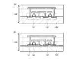
本実施の形態では、本発明の一態様に用いることのできるOSトランジスタについて図面を用いて説明する。なお、本実施の形態における図面では、明瞭化のために一部の要素を拡大、縮小、または省略して図示している。
本実施の形態では、実施の形態2に示したトランジスタの構成要素について詳細を説明する。
本実施の形態では、本発明の一態様に用いることのできる酸化物半導体の材料について説明する。
以下に、本発明に係る酸化物半導体について説明する。
以下では、本発明の一態様に用いることのできる酸化物半導体の構造について説明する。
本実施の形態では、イメージセンサチップを収めたパッケージおよびカメラモジュールの一例について説明する。当該イメージセンサチップには、本発明の一態様の撮像装置の構成を用いることができる。
本発明の一態様に係る撮像装置を用いることができる電子機器として、表示機器、パーソナルコンピュータ、記録媒体を備えた画像記憶装置または画像再生装置、携帯電話、携帯型を含むゲーム機、携帯データ端末、電子書籍端末、ビデオカメラ、デジタルスチルカメラなどのカメラ、ゴーグル型ディスプレイ(ヘッドマウントディスプレイ)、ナビゲーションシステム、音響再生装置(カーオーディオ、デジタルオーディオプレイヤーなど)、複写機、ファクシミリ、プリンタ、プリンタ複合機、現金自動預け入れ払い機(ATM)、自動販売機などが挙げられる。これら電子機器の具体例を図40に示す。
10a 画素
10b 画素
10c 画素
12 ロードライバ回路
13 CDS回路
14 A/D変換回路
15 カラムドライバ回路
16 画素アレイ
17 コンパレータ回路
18 カウンター回路
19 基板
21 光電変換素子
31 領域
32 領域
33 トランジスタ
34 トランジスタ
35 トランジスタ
41 領域
51 配線
53 配線
54 配線
60 絶縁体
61 導電体
62 導電体
63 絶縁体
64 半導体
64a 半導体
64b 半導体
64c 半導体
65 導電体
66 導電体
67 絶縁体
68 導電体
69 導電体
70 絶縁体
71 導電体
72 導電体
73 導電体
74 導電体
75 導電体
76 導電体
78 導電体
79 導電体
81 トランジスタ
82 トランジスタ
83 トランジスタ
84 容量素子
85 容量素子
91 配線
92 配線
93 配線
100 絶縁体
101 絶縁体
102 絶縁体
103 絶縁体
104 絶縁体
105 絶縁体
110 基板
111 配線
113 配線
120 導電体
121 導電体
130 シリコン基板
131 トランジスタ
132 トランジスタ
140 活性層
220 p+領域
230 p−領域
240 n型領域
250 p+領域
261 光電変換層
262 透光性導電体
263 半導体
264 半導体
265 半導体
266 電極
266a 導電体
266b 導電体
267 隔壁
268 正孔注入阻止層
269 電子注入阻止層
271 配線
271a 導電体
271b 導電体
288 配線
301 トランジスタ
302 トランジスタ
303 トランジスタ
304 トランジスタ
305 トランジスタ
306 トランジスタ
307 トランジスタ
310 基板
320 導電体
330 絶縁体
340 酸化物半導体
340a 酸化物半導体
340b 酸化物半導体
340c 酸化物半導体
340d 酸化物半導体
350 導電体
351 導電体
352 領域
353 領域
354 導電体
355 導電体
356 絶縁体
357 絶縁体
360 絶縁体
370 導電体
370a 導電体
370b 導電体
380 絶縁体
390 絶縁体
810 パッケージ基板
811 パッケージ基板
820 カバーガラス
821 レンズカバー
830 接着剤
835 レンズ
840 バンプ
841 ランド
850 イメージセンサチップ
851 イメージセンサチップ
860 電極パッド
861 電極パッド
870 ワイヤ
871 ワイヤ
880 スルーホール
885 ランド
890 ICチップ
901 筐体
902 筐体
903 表示部
904 表示部
905 マイク
906 スピーカー
907 操作キー
908 スタイラス
909 カメラ
911 筐体
912 表示部
919 カメラ
931 筐体
932 表示部
933 リストバンド
935 ボタン
936 竜頭
939 カメラ
951 筐体
952 レンズ
953 支持部
961 筐体
962 シャッターボタン
963 マイク
965 レンズ
967 発光部
971 筐体
972 筐体
973 表示部
974 操作キー
975 レンズ
976 接続部
1100 層
1200 層
1300 層
1400 層
1430 遮光層
1440 マイクロレンズアレイ
1450a 光学変換層
1450b 光電変換層
1450c 光電変換層
Claims (2)
- 光電変換素子と、前記光電変換素子に発生した電荷に応じて電位が変動するノードにゲートが電気的に接続されるトランジスタと、を含む画素を有する撮像装置であって、
第1の導電体と、第2の導電体と、第3の導電体と、第4の導電体と、第5の導電体と、第1の絶縁体と、第2の絶縁体と、酸化物半導体と、を前記画素に有し、
前記第1の導電体は、前記第1の絶縁体の下面と接し、
前記第1の絶縁体は、前記酸化物半導体の下面と接し、
前記酸化物半導体は、前記第2の導電体の下面と接し、
前記酸化物半導体は、前記第3の導電体の下面と接し、
前記酸化物半導体は、前記第2の絶縁体の下面と接し、
前記第2の導電体は、前記第2の絶縁体の下面と接し、
前記第3の導電体は、前記第2の絶縁体の下面と接し、
前記第2の絶縁体は、前記第4の導電体の下面と接し、
前記第2の絶縁体は、前記第5の導電体の下面と接し、
前記第1の導電体は、前記第4の導電体と重なる領域を有し、
前記第1の導電体は、前記第5の導電体と重なる領域を有し、
前記第2の導電体は、前記第4の導電体と重なる領域を有し、
前記第3の導電体は、前記第5の導電体と重なる領域を有し、
前記第1の導電体、前記第4の導電体、及び前記第5の導電体は、ゲート電極としての機能を有し、
前記第1の絶縁体はゲート絶縁膜としての機能を有し、
前記第2の絶縁体はゲート絶縁膜としての機能を有し、
前記第2の導電体は、前記光電変換素子の一方の電極と電気的に接続され、
前記第3の導電体は、前記トランジスタのゲートと電気的に接続される、撮像装置。 - 請求項1において、
第6の導電体と、第7の導電体と、を有し、
前記第6の導電体は前記第1の絶縁体の下面と接し、
前記第7の導電体は前記第1の絶縁体の下面と接し、
前記第6の導電体は前記第4の導電体と重なる領域を有し、
前記第7の導電体は前記第5の導電体と重なる領域を有し、
前記第6の導電体及び前記第7の導電体は、ゲート電極としての機能を有する、撮像装置。
Applications Claiming Priority (2)
| Application Number | Priority Date | Filing Date | Title |
|---|---|---|---|
| JP2016044271 | 2016-03-08 | ||
| JP2016044271 | 2016-03-08 |
Publications (2)
| Publication Number | Publication Date |
|---|---|
| JP2017163139A JP2017163139A (ja) | 2017-09-14 |
| JP6904730B2 true JP6904730B2 (ja) | 2021-07-21 |
Family
ID=59788642
Family Applications (1)
| Application Number | Title | Priority Date | Filing Date |
|---|---|---|---|
| JP2017037883A Active JP6904730B2 (ja) | 2016-03-08 | 2017-03-01 | 撮像装置 |
Country Status (2)
| Country | Link |
|---|---|
| US (2) | US10014334B2 (ja) |
| JP (1) | JP6904730B2 (ja) |
Families Citing this family (5)
| Publication number | Priority date | Publication date | Assignee | Title |
|---|---|---|---|---|
| US10529740B2 (en) * | 2013-07-25 | 2020-01-07 | Semiconductor Energy Laboratory Co., Ltd. | Semiconductor device including semiconductor layer and conductive layer |
| JP7110987B2 (ja) * | 2016-12-05 | 2022-08-02 | 凸版印刷株式会社 | 固体撮像素子 |
| CN109997352B (zh) * | 2016-12-27 | 2021-06-01 | 松下知识产权经营株式会社 | 摄像装置、相机以及摄像方法 |
| CN111653645A (zh) * | 2020-06-15 | 2020-09-11 | 京东方科技集团股份有限公司 | 一种探测面板、其制作方法及射线探测装置 |
| JP7626687B2 (ja) * | 2021-08-19 | 2025-02-04 | 株式会社ジャパンディスプレイ | 検出装置 |
Family Cites Families (124)
| Publication number | Priority date | Publication date | Assignee | Title |
|---|---|---|---|---|
| JPS60198861A (ja) | 1984-03-23 | 1985-10-08 | Fujitsu Ltd | 薄膜トランジスタ |
| JPH0244256B2 (ja) | 1987-01-28 | 1990-10-03 | Kagaku Gijutsucho Mukizaishitsu Kenkyushocho | Ingazn2o5deshimesarerurotsuhoshokeinosojokozoojusurukagobutsuoyobisonoseizoho |
| JPH0244260B2 (ja) | 1987-02-24 | 1990-10-03 | Kagaku Gijutsucho Mukizaishitsu Kenkyushocho | Ingazn5o8deshimesarerurotsuhoshokeinosojokozoojusurukagobutsuoyobisonoseizoho |
| JPH0244258B2 (ja) | 1987-02-24 | 1990-10-03 | Kagaku Gijutsucho Mukizaishitsu Kenkyushocho | Ingazn3o6deshimesarerurotsuhoshokeinosojokozoojusurukagobutsuoyobisonoseizoho |
| JPS63210023A (ja) | 1987-02-24 | 1988-08-31 | Natl Inst For Res In Inorg Mater | InGaZn↓4O↓7で示される六方晶系の層状構造を有する化合物およびその製造法 |
| JPH0244262B2 (ja) | 1987-02-27 | 1990-10-03 | Kagaku Gijutsucho Mukizaishitsu Kenkyushocho | Ingazn6o9deshimesarerurotsuhoshokeinosojokozoojusurukagobutsuoyobisonoseizoho |
| JPH0244263B2 (ja) | 1987-04-22 | 1990-10-03 | Kagaku Gijutsucho Mukizaishitsu Kenkyushocho | Ingazn7o10deshimesarerurotsuhoshokeinosojokozoojusurukagobutsuoyobisonoseizoho |
| JPH05251705A (ja) | 1992-03-04 | 1993-09-28 | Fuji Xerox Co Ltd | 薄膜トランジスタ |
| JP3479375B2 (ja) | 1995-03-27 | 2003-12-15 | 科学技術振興事業団 | 亜酸化銅等の金属酸化物半導体による薄膜トランジスタとpn接合を形成した金属酸化物半導体装置およびそれらの製造方法 |
| JPH11505377A (ja) | 1995-08-03 | 1999-05-18 | フィリップス エレクトロニクス ネムローゼ フェンノートシャップ | 半導体装置 |
| JPH0990405A (ja) * | 1995-09-21 | 1997-04-04 | Sharp Corp | 薄膜トランジスタ |
| JP3625598B2 (ja) | 1995-12-30 | 2005-03-02 | 三星電子株式会社 | 液晶表示装置の製造方法 |
| JP4170454B2 (ja) | 1998-07-24 | 2008-10-22 | Hoya株式会社 | 透明導電性酸化物薄膜を有する物品及びその製造方法 |
| JP2000150861A (ja) | 1998-11-16 | 2000-05-30 | Tdk Corp | 酸化物薄膜 |
| JP3276930B2 (ja) | 1998-11-17 | 2002-04-22 | 科学技術振興事業団 | トランジスタ及び半導体装置 |
| TW460731B (en) | 1999-09-03 | 2001-10-21 | Ind Tech Res Inst | Electrode structure and production method of wide viewing angle LCD |
| JP4089858B2 (ja) | 2000-09-01 | 2008-05-28 | 国立大学法人東北大学 | 半導体デバイス |
| KR20020038482A (ko) | 2000-11-15 | 2002-05-23 | 모리시타 요이찌 | 박막 트랜지스터 어레이, 그 제조방법 및 그것을 이용한표시패널 |
| JP3997731B2 (ja) | 2001-03-19 | 2007-10-24 | 富士ゼロックス株式会社 | 基材上に結晶性半導体薄膜を形成する方法 |
| JP2002289859A (ja) | 2001-03-23 | 2002-10-04 | Minolta Co Ltd | 薄膜トランジスタ |
| JP4003549B2 (ja) * | 2001-06-28 | 2007-11-07 | 日本ビクター株式会社 | 固体撮像装置 |
| JP3925839B2 (ja) | 2001-09-10 | 2007-06-06 | シャープ株式会社 | 半導体記憶装置およびその試験方法 |
| JP4090716B2 (ja) | 2001-09-10 | 2008-05-28 | 雅司 川崎 | 薄膜トランジスタおよびマトリクス表示装置 |
| JP4164562B2 (ja) | 2002-09-11 | 2008-10-15 | 独立行政法人科学技術振興機構 | ホモロガス薄膜を活性層として用いる透明薄膜電界効果型トランジスタ |
| EP1443130B1 (en) | 2001-11-05 | 2011-09-28 | Japan Science and Technology Agency | Natural superlattice homologous single crystal thin film, method for preparation thereof, and device using said single crystal thin film |
| JP4083486B2 (ja) | 2002-02-21 | 2008-04-30 | 独立行政法人科学技術振興機構 | LnCuO(S,Se,Te)単結晶薄膜の製造方法 |
| US7049190B2 (en) | 2002-03-15 | 2006-05-23 | Sanyo Electric Co., Ltd. | Method for forming ZnO film, method for forming ZnO semiconductor layer, method for fabricating semiconductor device, and semiconductor device |
| JP3933591B2 (ja) | 2002-03-26 | 2007-06-20 | 淳二 城戸 | 有機エレクトロルミネッセント素子 |
| US7339187B2 (en) | 2002-05-21 | 2008-03-04 | State Of Oregon Acting By And Through The Oregon State Board Of Higher Education On Behalf Of Oregon State University | Transistor structures |
| JP2004022625A (ja) | 2002-06-13 | 2004-01-22 | Murata Mfg Co Ltd | 半導体デバイス及び該半導体デバイスの製造方法 |
| US7105868B2 (en) | 2002-06-24 | 2006-09-12 | Cermet, Inc. | High-electron mobility transistor with zinc oxide |
| US7067843B2 (en) | 2002-10-11 | 2006-06-27 | E. I. Du Pont De Nemours And Company | Transparent oxide semiconductor thin film transistors |
| JP4166105B2 (ja) | 2003-03-06 | 2008-10-15 | シャープ株式会社 | 半導体装置およびその製造方法 |
| JP2004273732A (ja) | 2003-03-07 | 2004-09-30 | Sharp Corp | アクティブマトリクス基板およびその製造方法 |
| JP4108633B2 (ja) | 2003-06-20 | 2008-06-25 | シャープ株式会社 | 薄膜トランジスタおよびその製造方法ならびに電子デバイス |
| US7262463B2 (en) | 2003-07-25 | 2007-08-28 | Hewlett-Packard Development Company, L.P. | Transistor including a deposited channel region having a doped portion |
| US7282782B2 (en) | 2004-03-12 | 2007-10-16 | Hewlett-Packard Development Company, L.P. | Combined binary oxide semiconductor device |
| EP1737044B1 (en) | 2004-03-12 | 2014-12-10 | Japan Science and Technology Agency | Amorphous oxide and thin film transistor |
| US7297977B2 (en) | 2004-03-12 | 2007-11-20 | Hewlett-Packard Development Company, L.P. | Semiconductor device |
| US7145174B2 (en) | 2004-03-12 | 2006-12-05 | Hewlett-Packard Development Company, Lp. | Semiconductor device |
| US7211825B2 (en) | 2004-06-14 | 2007-05-01 | Yi-Chi Shih | Indium oxide-based thin film transistors and circuits |
| JP2006100760A (ja) | 2004-09-02 | 2006-04-13 | Casio Comput Co Ltd | 薄膜トランジスタおよびその製造方法 |
| US7285501B2 (en) | 2004-09-17 | 2007-10-23 | Hewlett-Packard Development Company, L.P. | Method of forming a solution processed device |
| US7298084B2 (en) | 2004-11-02 | 2007-11-20 | 3M Innovative Properties Company | Methods and displays utilizing integrated zinc oxide row and column drivers in conjunction with organic light emitting diodes |
| RU2358354C2 (ru) | 2004-11-10 | 2009-06-10 | Кэнон Кабусики Кайся | Светоизлучающее устройство |
| US7829444B2 (en) | 2004-11-10 | 2010-11-09 | Canon Kabushiki Kaisha | Field effect transistor manufacturing method |
| KR100998527B1 (ko) | 2004-11-10 | 2010-12-07 | 고쿠리츠다이가쿠호진 토쿄고교 다이가꾸 | 비정질 산화물 및 전계 효과 트랜지스터 |
| US7791072B2 (en) | 2004-11-10 | 2010-09-07 | Canon Kabushiki Kaisha | Display |
| EP1815530B1 (en) | 2004-11-10 | 2021-02-17 | Canon Kabushiki Kaisha | Field effect transistor employing an amorphous oxide |
| US7453065B2 (en) | 2004-11-10 | 2008-11-18 | Canon Kabushiki Kaisha | Sensor and image pickup device |
| US7863611B2 (en) | 2004-11-10 | 2011-01-04 | Canon Kabushiki Kaisha | Integrated circuits utilizing amorphous oxides |
| US7579224B2 (en) | 2005-01-21 | 2009-08-25 | Semiconductor Energy Laboratory Co., Ltd. | Method for manufacturing a thin film semiconductor device |
| TWI481024B (zh) | 2005-01-28 | 2015-04-11 | 半導體能源研究所股份有限公司 | 半導體裝置,電子裝置,和半導體裝置的製造方法 |
| TWI505473B (zh) | 2005-01-28 | 2015-10-21 | 半導體能源研究所股份有限公司 | 半導體裝置,電子裝置,和半導體裝置的製造方法 |
| US7858451B2 (en) | 2005-02-03 | 2010-12-28 | Semiconductor Energy Laboratory Co., Ltd. | Electronic device, semiconductor device and manufacturing method thereof |
| US7948171B2 (en) | 2005-02-18 | 2011-05-24 | Semiconductor Energy Laboratory Co., Ltd. | Light emitting device |
| US20060197092A1 (en) | 2005-03-03 | 2006-09-07 | Randy Hoffman | System and method for forming conductive material on a substrate |
| US8681077B2 (en) | 2005-03-18 | 2014-03-25 | Semiconductor Energy Laboratory Co., Ltd. | Semiconductor device, and display device, driving method and electronic apparatus thereof |
| US7544967B2 (en) | 2005-03-28 | 2009-06-09 | Massachusetts Institute Of Technology | Low voltage flexible organic/transparent transistor for selective gas sensing, photodetecting and CMOS device applications |
| US7645478B2 (en) | 2005-03-31 | 2010-01-12 | 3M Innovative Properties Company | Methods of making displays |
| US8300031B2 (en) | 2005-04-20 | 2012-10-30 | Semiconductor Energy Laboratory Co., Ltd. | Semiconductor device comprising transistor having gate and drain connected through a current-voltage conversion element |
| JP2006344849A (ja) | 2005-06-10 | 2006-12-21 | Casio Comput Co Ltd | 薄膜トランジスタ |
| US7691666B2 (en) | 2005-06-16 | 2010-04-06 | Eastman Kodak Company | Methods of making thin film transistors comprising zinc-oxide-based semiconductor materials and transistors made thereby |
| US7402506B2 (en) | 2005-06-16 | 2008-07-22 | Eastman Kodak Company | Methods of making thin film transistors comprising zinc-oxide-based semiconductor materials and transistors made thereby |
| US7507618B2 (en) | 2005-06-27 | 2009-03-24 | 3M Innovative Properties Company | Method for making electronic devices using metal oxide nanoparticles |
| KR100711890B1 (ko) | 2005-07-28 | 2007-04-25 | 삼성에스디아이 주식회사 | 유기 발광표시장치 및 그의 제조방법 |
| JP2007059128A (ja) | 2005-08-23 | 2007-03-08 | Canon Inc | 有機el表示装置およびその製造方法 |
| JP5116225B2 (ja) | 2005-09-06 | 2013-01-09 | キヤノン株式会社 | 酸化物半導体デバイスの製造方法 |
| JP4280736B2 (ja) | 2005-09-06 | 2009-06-17 | キヤノン株式会社 | 半導体素子 |
| JP4850457B2 (ja) | 2005-09-06 | 2012-01-11 | キヤノン株式会社 | 薄膜トランジスタ及び薄膜ダイオード |
| JP2007073705A (ja) | 2005-09-06 | 2007-03-22 | Canon Inc | 酸化物半導体チャネル薄膜トランジスタおよびその製造方法 |
| EP1998373A3 (en) | 2005-09-29 | 2012-10-31 | Semiconductor Energy Laboratory Co, Ltd. | Semiconductor device having oxide semiconductor layer and manufacturing method thereof |
| KR100775058B1 (ko) * | 2005-09-29 | 2007-11-08 | 삼성전자주식회사 | 픽셀 및 이를 이용한 이미지 센서, 그리고 상기 이미지센서를 포함하는 이미지 처리 시스템 |
| JP5037808B2 (ja) | 2005-10-20 | 2012-10-03 | キヤノン株式会社 | アモルファス酸化物を用いた電界効果型トランジスタ、及び該トランジスタを用いた表示装置 |
| CN101577231B (zh) | 2005-11-15 | 2013-01-02 | 株式会社半导体能源研究所 | 半导体器件及其制造方法 |
| TWI292281B (en) | 2005-12-29 | 2008-01-01 | Ind Tech Res Inst | Pixel structure of active organic light emitting diode and method of fabricating the same |
| US7867636B2 (en) | 2006-01-11 | 2011-01-11 | Murata Manufacturing Co., Ltd. | Transparent conductive film and method for manufacturing the same |
| JP4977478B2 (ja) | 2006-01-21 | 2012-07-18 | 三星電子株式会社 | ZnOフィルム及びこれを用いたTFTの製造方法 |
| US7576394B2 (en) | 2006-02-02 | 2009-08-18 | Kochi Industrial Promotion Center | Thin film transistor including low resistance conductive thin films and manufacturing method thereof |
| US7977169B2 (en) | 2006-02-15 | 2011-07-12 | Kochi Industrial Promotion Center | Semiconductor device including active layer made of zinc oxide with controlled orientations and manufacturing method thereof |
| KR20070101595A (ko) | 2006-04-11 | 2007-10-17 | 삼성전자주식회사 | ZnO TFT |
| US20070252928A1 (en) | 2006-04-28 | 2007-11-01 | Toppan Printing Co., Ltd. | Structure, transmission type liquid crystal display, reflection type display and manufacturing method thereof |
| JP5028033B2 (ja) | 2006-06-13 | 2012-09-19 | キヤノン株式会社 | 酸化物半導体膜のドライエッチング方法 |
| JP4609797B2 (ja) | 2006-08-09 | 2011-01-12 | Nec液晶テクノロジー株式会社 | 薄膜デバイス及びその製造方法 |
| JP4999400B2 (ja) | 2006-08-09 | 2012-08-15 | キヤノン株式会社 | 酸化物半導体膜のドライエッチング方法 |
| JP4332545B2 (ja) | 2006-09-15 | 2009-09-16 | キヤノン株式会社 | 電界効果型トランジスタ及びその製造方法 |
| JP4274219B2 (ja) | 2006-09-27 | 2009-06-03 | セイコーエプソン株式会社 | 電子デバイス、有機エレクトロルミネッセンス装置、有機薄膜半導体装置 |
| JP5164357B2 (ja) | 2006-09-27 | 2013-03-21 | キヤノン株式会社 | 半導体装置及び半導体装置の製造方法 |
| US7622371B2 (en) | 2006-10-10 | 2009-11-24 | Hewlett-Packard Development Company, L.P. | Fused nanocrystal thin film semiconductor and method |
| US7772021B2 (en) | 2006-11-29 | 2010-08-10 | Samsung Electronics Co., Ltd. | Flat panel displays comprising a thin-film transistor having a semiconductive oxide in its channel and methods of fabricating the same for use in flat panel displays |
| JP2008140684A (ja) | 2006-12-04 | 2008-06-19 | Toppan Printing Co Ltd | カラーelディスプレイおよびその製造方法 |
| KR101303578B1 (ko) | 2007-01-05 | 2013-09-09 | 삼성전자주식회사 | 박막 식각 방법 |
| US8207063B2 (en) | 2007-01-26 | 2012-06-26 | Eastman Kodak Company | Process for atomic layer deposition |
| KR100851215B1 (ko) | 2007-03-14 | 2008-08-07 | 삼성에스디아이 주식회사 | 박막 트랜지스터 및 이를 이용한 유기 전계 발광표시장치 |
| US7795613B2 (en) | 2007-04-17 | 2010-09-14 | Toppan Printing Co., Ltd. | Structure with transistor |
| KR101325053B1 (ko) | 2007-04-18 | 2013-11-05 | 삼성디스플레이 주식회사 | 박막 트랜지스터 기판 및 이의 제조 방법 |
| KR20080094300A (ko) | 2007-04-19 | 2008-10-23 | 삼성전자주식회사 | 박막 트랜지스터 및 그 제조 방법과 박막 트랜지스터를포함하는 평판 디스플레이 |
| KR101334181B1 (ko) | 2007-04-20 | 2013-11-28 | 삼성전자주식회사 | 선택적으로 결정화된 채널층을 갖는 박막 트랜지스터 및 그제조 방법 |
| WO2008133345A1 (en) | 2007-04-25 | 2008-11-06 | Canon Kabushiki Kaisha | Oxynitride semiconductor |
| KR101345376B1 (ko) | 2007-05-29 | 2013-12-24 | 삼성전자주식회사 | ZnO 계 박막 트랜지스터 및 그 제조방법 |
| KR101404074B1 (ko) * | 2007-07-31 | 2014-06-05 | 삼성전기주식회사 | Cmos 영상 센서 |
| US8202365B2 (en) | 2007-12-17 | 2012-06-19 | Fujifilm Corporation | Process for producing oriented inorganic crystalline film, and semiconductor device using the oriented inorganic crystalline film |
| JP4623179B2 (ja) | 2008-09-18 | 2011-02-02 | ソニー株式会社 | 薄膜トランジスタおよびその製造方法 |
| JP5451280B2 (ja) | 2008-10-09 | 2014-03-26 | キヤノン株式会社 | ウルツ鉱型結晶成長用基板およびその製造方法ならびに半導体装置 |
| KR101432764B1 (ko) * | 2008-11-13 | 2014-08-21 | 가부시키가이샤 한도오따이 에네루기 켄큐쇼 | 반도체장치의 제조방법 |
| WO2011027656A1 (en) * | 2009-09-04 | 2011-03-10 | Semiconductor Energy Laboratory Co., Ltd. | Transistor and display device |
| KR102114011B1 (ko) | 2010-01-15 | 2020-05-22 | 가부시키가이샤 한도오따이 에네루기 켄큐쇼 | 반도체 장치 및 이를 구동하는 방법 |
| DE112011100842T5 (de) | 2010-03-08 | 2013-01-17 | Semiconductor Energy Laboratory Co., Ltd. | Halbleiterbauelement und Verfahren zu dessen Herstellung |
| CN102782622B (zh) | 2010-03-12 | 2016-11-02 | 株式会社半导体能源研究所 | 显示装置的驱动方法 |
| JP2012147187A (ja) * | 2011-01-11 | 2012-08-02 | Olympus Imaging Corp | 撮像装置 |
| JP5821315B2 (ja) | 2011-06-21 | 2015-11-24 | ソニー株式会社 | 電子機器、電子機器の駆動方法 |
| US8836626B2 (en) | 2011-07-15 | 2014-09-16 | Semiconductor Energy Laboratory Co., Ltd. | Semiconductor device and method for driving the same |
| US9490373B2 (en) * | 2012-02-02 | 2016-11-08 | Sony Corporation | Solid-state imaging device and electronic apparatus with improved storage portion |
| KR102269460B1 (ko) * | 2013-06-27 | 2021-06-28 | 가부시키가이샤 한도오따이 에네루기 켄큐쇼 | 반도체 장치 |
| JP2015023250A (ja) | 2013-07-23 | 2015-02-02 | ソニー株式会社 | 固体撮像素子及びその駆動方法、並びに電子機器 |
| JP2015041677A (ja) * | 2013-08-21 | 2015-03-02 | ルネサスエレクトロニクス株式会社 | 半導体装置およびその製造方法 |
| TWI706550B (zh) * | 2013-11-06 | 2020-10-01 | 日商新力股份有限公司 | 固體攝像裝置及其製造方法、及電子機器 |
| KR102380829B1 (ko) * | 2014-04-23 | 2022-03-31 | 가부시키가이샤 한도오따이 에네루기 켄큐쇼 | 촬상 장치 |
| JP6260787B2 (ja) * | 2014-05-23 | 2018-01-17 | パナソニックIpマネジメント株式会社 | 撮像装置 |
| KR102509203B1 (ko) | 2014-08-29 | 2023-03-14 | 가부시키가이샤 한도오따이 에네루기 켄큐쇼 | 촬상 장치 및 전자 기기 |
| WO2016055909A1 (en) * | 2014-10-10 | 2016-04-14 | Semiconductor Energy Laboratory Co., Ltd. | Imaging device |
| WO2016092427A1 (en) * | 2014-12-10 | 2016-06-16 | Semiconductor Energy Laboratory Co., Ltd. | Semiconductor device and method for manufacturing the same |
| JP6555468B2 (ja) * | 2015-04-02 | 2019-08-07 | パナソニックIpマネジメント株式会社 | 撮像装置 |
| US10020336B2 (en) * | 2015-12-28 | 2018-07-10 | Semiconductor Energy Laboratory Co., Ltd. | Imaging device and electronic device using three dimentional (3D) integration |
-
2017
- 2017-03-01 JP JP2017037883A patent/JP6904730B2/ja active Active
- 2017-03-02 US US15/447,801 patent/US10014334B2/en active Active
-
2018
- 2018-06-28 US US16/021,146 patent/US10256265B2/en active Active
Also Published As
| Publication number | Publication date |
|---|---|
| US20170263661A1 (en) | 2017-09-14 |
| US20180308886A1 (en) | 2018-10-25 |
| US10256265B2 (en) | 2019-04-09 |
| JP2017163139A (ja) | 2017-09-14 |
| US10014334B2 (en) | 2018-07-03 |
Similar Documents
| Publication | Publication Date | Title |
|---|---|---|
| JP6959468B2 (ja) | カメラモジュール、及び、電子機器 | |
| JP6811342B2 (ja) | 光電変換装置 | |
| JP6755756B2 (ja) | 撮像装置 | |
| JP6960025B2 (ja) | 撮像装置 | |
| JP7085595B2 (ja) | 撮像装置 | |
| JP6737633B2 (ja) | 撮像装置および電子機器 | |
| JP7020783B2 (ja) | 撮像装置 | |
| JP7114783B2 (ja) | 撮像素子 | |
| JP2022043162A (ja) | 撮像装置 | |
| JP6904730B2 (ja) | 撮像装置 | |
| JP6903413B2 (ja) | 撮像装置、モジュール、および電子機器 | |
| JP2020171023A (ja) | 電子機器および撮像装置 |
Legal Events
| Date | Code | Title | Description |
|---|---|---|---|
| A621 | Written request for application examination |
Free format text: JAPANESE INTERMEDIATE CODE: A621 Effective date: 20200217 |
|
| A977 | Report on retrieval |
Free format text: JAPANESE INTERMEDIATE CODE: A971007 Effective date: 20201225 |
|
| A131 | Notification of reasons for refusal |
Free format text: JAPANESE INTERMEDIATE CODE: A131 Effective date: 20210126 |
|
| A521 | Request for written amendment filed |
Free format text: JAPANESE INTERMEDIATE CODE: A523 Effective date: 20210311 |
|
| A131 | Notification of reasons for refusal |
Free format text: JAPANESE INTERMEDIATE CODE: A131 Effective date: 20210330 |
|
| A521 | Request for written amendment filed |
Free format text: JAPANESE INTERMEDIATE CODE: A523 Effective date: 20210506 |
|
| TRDD | Decision of grant or rejection written | ||
| A01 | Written decision to grant a patent or to grant a registration (utility model) |
Free format text: JAPANESE INTERMEDIATE CODE: A01 Effective date: 20210601 |
|
| A61 | First payment of annual fees (during grant procedure) |
Free format text: JAPANESE INTERMEDIATE CODE: A61 Effective date: 20210624 |
|
| R150 | Certificate of patent or registration of utility model |
Ref document number: 6904730 Country of ref document: JP Free format text: JAPANESE INTERMEDIATE CODE: R150 |
|
| R250 | Receipt of annual fees |
Free format text: JAPANESE INTERMEDIATE CODE: R250 |
|
| R250 | Receipt of annual fees |
Free format text: JAPANESE INTERMEDIATE CODE: R250 |