JP6232690B2 - Imaging apparatus, illumination control method, and program - Google Patents
Imaging apparatus, illumination control method, and program Download PDFInfo
- Publication number
- JP6232690B2 JP6232690B2 JP2012061878A JP2012061878A JP6232690B2 JP 6232690 B2 JP6232690 B2 JP 6232690B2 JP 2012061878 A JP2012061878 A JP 2012061878A JP 2012061878 A JP2012061878 A JP 2012061878A JP 6232690 B2 JP6232690 B2 JP 6232690B2
- Authority
- JP
- Japan
- Prior art keywords
- voltage
- light emitting
- unit
- imaging
- light
- Prior art date
- Legal status (The legal status is an assumption and is not a legal conclusion. Google has not performed a legal analysis and makes no representation as to the accuracy of the status listed.)
- Expired - Fee Related
Links
Images


Landscapes
- Stroboscope Apparatuses (AREA)
- Studio Devices (AREA)
Description
本発明は、発光部を備えた撮像装置、照明制御方法及びプログラムに関する。 The present invention relates to an imaging device including a light emitting unit, an illumination control method, and a program.
従来より、デジタルカメラに搭載されるストロボシステムの多くは、発光部としてキセノンライトを含む構成が広く採用されていた。 Conventionally, many strobe systems mounted on digital cameras have widely adopted a configuration including a xenon light as a light emitting unit.
近年のストロボシステムの中には、高輝度なLED(Light Emitting Diode:発光ダイオード)を発光部として含むものも存在する。このようなストロボシステムを、以下、「LEDストロボシステム」と呼ぶ。 Some recent strobe systems include a high-luminance LED (Light Emitting Diode) as a light emitting unit. Such a strobe system is hereinafter referred to as an “LED strobe system”.
このようなLEDストロボシステムにおいては、大発光量が必要であるため、非常に大きな電流IFがLEDに流れる必要がある。
ただし、LEDには、電流IFが高値になるに連れて電圧VFも高値になるという特徴が存在する。この特徴のために、一定値以下の電圧VFでしかLEDに印加できないような環境では、LEDの電流IFが、LEDストロボシステムにとって必要な値に到達しないおそれがある。
このようなことから、現在一般的に開発が進んでいるLEDストロボシステムでは、LEDと、昇圧回路と、定電流/発光回路と、EDLC(Electric Double−Layer Capacitor:電気二重層キャパシタ)と、EDLC充電回路と、で構成されているものがある。
このようなLEDストロボシステムの昇圧回路で生成する電圧は、
・EDLCの内部のインピーダンスのバラツキ、温度特性及び経年変化
・定電流回路の損失
・LEDの電圧VFのバラツキ、温度特性及び経年変化
等を考慮した上で決める必要がある。
特にEDLC等を用いるケースでは、高い電圧を印加すると劣化が生じるため、できるだけ低い電圧で動作させるのが好ましい。
ここでEDLC等のLEDストロボの発光に係るデバイスの劣化を抑制する技術としては、特許文献1に記載の技術が知られている。
この特許文献1には、LEDストロボを発光させる際、電池の種類、温度又は充放電回数等の過去の使用状況によって充電させるべき電圧値を調整することにより、デバイスの劣化を抑制する技術が記載されている。
In such an LED strobe system, since a large amount of light emission is required, a very large current IF needs to flow through the LED.
However, the LED has a feature that the voltage VF becomes higher as the current IF becomes higher. Due to this feature, the LED current IF may not reach the value required for the LED strobe system in an environment where the LED can only be applied at a voltage VF below a certain value.
For this reason, in LED strobe systems that are currently being developed in general, LEDs, booster circuits, constant current / light emitting circuits, EDLCs (Electronic Double-Layer Capacitors), and EDLCs And a charging circuit.
The voltage generated by the booster circuit of such an LED strobe system is
-It is necessary to decide in consideration of variations in internal impedance of EDLC, temperature characteristics and aging, loss of constant current circuit, variation in LED voltage VF, temperature characteristics and aging.
In particular, in the case of using EDLC or the like, it is preferable to operate at as low a voltage as possible because deterioration occurs when a high voltage is applied.
Here, as a technique for suppressing deterioration of a device related to light emission of an LED strobe such as EDLC, a technique described in
This
しかしながら、上述した特許文献1に記載の技術では、電池の種類や過去の使用状況によって充電させるべき電圧値を決めるために、発光時の状況が考慮されておらず、発光部の劣化の抑制が行われていない可能性があった。
However, in the technique described in
本発明は、このような状況に鑑みてなされたものであり、発光部の劣化を確実に抑制することができる撮像装置、照明制御方法及びプログラムを提供することを目的とする。 The present invention has been made in view of such a situation, and an object thereof is to provide an imaging device, an illumination control method, and a program capable of reliably suppressing deterioration of a light emitting unit.
上記目的を達成するため、本発明の一態様の撮像装置は、電圧が印加されることにより発光する発光手段と、画像を撮像する撮像手段と、前記発光手段に電圧を印加する電圧印加手段と、前記電圧印加手段によって電圧が印加されて前記発光手段が発光すると、この時の発光状態に対応する印加電圧値とこれ以前に発光した所望の発光状態に対応する印加電圧値との誤差に基づいて、今回の撮像における印加電圧値を取得する取得手段と、前記取得手段によって取得された印加電圧値の電圧を前記発光手段に印加するよう前記電圧印加手段を制御する電圧印加制御手段と、前記電圧印加制御手段による制御により発光手段が発光した時に前記撮像手段が撮像した画像のデータを所定の記録媒体に記録するように制御する記録制御手段と、を備えたことを特徴とする。 In order to achieve the above object, an imaging device of one embodiment of the present invention includes a light emitting unit that emits light when a voltage is applied thereto, an imaging unit that captures an image, and a voltage applying unit that applies a voltage to the light emitting unit. When the voltage is applied by the voltage applying means and the light emitting means emits light , based on an error between an applied voltage value corresponding to the light emitting state at this time and an applied voltage value corresponding to a desired light emitting state previously emitted. Acquisition means for acquiring an applied voltage value in the current imaging, voltage application control means for controlling the voltage application means to apply the voltage of the applied voltage value acquired by the acquisition means to the light emitting means, and Recording control means for controlling the image data captured by the imaging means to be recorded on a predetermined recording medium when the light emitting means emits light under the control of the voltage application control means. Characterized in that was.
本発明によれば、発光部の劣化を確実に抑制することができる。 According to the present invention, it is possible to reliably suppress deterioration of the light emitting unit.
以下、本発明の実施形態について、図面を用いて説明する。 Hereinafter, embodiments of the present invention will be described with reference to the drawings.
図1は、本発明の一実施形態に係る撮像装置1のハードウェアの構成を示すブロック図である。
撮像装置1は、例えばデジタルカメラして構成される。
FIG. 1 is a block diagram showing a hardware configuration of an
The
撮像装置1は、図1に示すように、制御部11と、メモリデバイス12と、撮像部13と、A/D(Analog/Digital)変換部14と、レンズ駆動部15と、駆動機構16と、発光部17と、電圧印加部18と、発光状態検出部19と、表示部20と、操作部21と、メモリカード装着部22と、USB(Universal Serial Bus)コネクタ23と、電源24と、を備える。
As shown in FIG. 1, the
制御部11は、CPU(Central Processing Unit)等で構成され、メモリデバイス12等に記録されているプログラムや、メモリデバイス12等にロードされたプログラムに従って各種の処理を実行する。
The
メモリデバイス12は、例えばROM(Read Only Memory)やRAM(Random Access Memory)等の種々のメモリデバイス12によって構成され各種データを記憶する。
The
撮像部13は、図示はしないが、光学レンズ部と、イメージセンサと、を備えている。
光学レンズ部は、被写体を撮影するために、光を集光するレンズ、例えばフォーカスレンズやズームレンズ等で構成される。
フォーカスレンズは、イメージセンサの受光面に被写体像を結像させるレンズである。ズームレンズは、焦点距離を一定の範囲で自在に変化させるレンズである。
光学レンズ部にはまた、必要に応じて、焦点、露出、ホワイトバランス等の設定パラメータを調整する周辺回路が設けられる。
Although not shown, the
The optical lens unit is configured by a lens that collects light, for example, a focus lens or a zoom lens, in order to photograph a subject.
The focus lens is a lens that forms a subject image on the light receiving surface of the image sensor. The zoom lens is a lens that freely changes the focal length within a certain range.
The optical lens unit is also provided with a peripheral circuit for adjusting setting parameters such as focus, exposure, and white balance as necessary.
イメージセンサは、光電変換素子や、AFE(Analog Front End)等から構成される。
光電変換素子は、例えばCMOS(Complementary Metal Oxide Semiconductor)型の光電変換素子等から構成される。光電変換素子には、光学レンズ部から被写体像が入射される。そこで、光電変換素子は、被写体像を光電変換(撮像)して画像信号を一定時間蓄積し、蓄積した画像信号をアナログ信号としてA/D変換部14に順次供給する。
A/D変換部14は、撮像部13のイメージセンサから供給されたアナログの画像信号に対して、A/D変換処理等の各種信号処理を施す。各種信号処理によって、デジタル信号が生成され、制御部11に供給される。
このような撮像部13からA/D変換部14を経由して制御部11に供給されるデジタル信号を、以下、「撮像画像のデータ」と呼ぶ。
The image sensor includes a photoelectric conversion element, AFE (Analog Front End), and the like.
The photoelectric conversion element is composed of, for example, a CMOS (Complementary Metal Oxide Semiconductor) type photoelectric conversion element or the like. A subject image is incident on the photoelectric conversion element from the optical lens unit. Therefore, the photoelectric conversion element photoelectrically converts (captures) the subject image, accumulates the image signal for a predetermined time, and sequentially supplies the accumulated image signal to the A /
The A /
Such a digital signal supplied from the
レンズ駆動部15は、制御部11からの制御の下、駆動機構に指令を発行する。
駆動機構16は、レンズ駆動部15からの指令に従い、撮像部13の図示せぬレンズユニットを駆動させる。
The
The
発光部17は、1以上のLEDからなるLED部31と、EDLC部32と、を含むように構成される、印加された電圧の値に応じた光量で発光する。
電圧印加部18は、昇圧回路により構成され、制御部11の制御の下、所定の値の電圧を発光部17に対して印加する。
発光状態検出部19は、電圧印加部18により電圧が印加されている際の発光部17の発光状態を検出し、制御部11に供給する。発光状態検出部19により検出される発光状態は、LED部31の発光量に応じて可変する状態であれば足り、特に限定されないが、本実施形態では、LED部31の電流IFの値であるものとする。
このように、本実施形態では、発光部17、電圧印加部18、及び発光状態検出部19により、LEDストロボシステムが構築される。
The
The
The light emission
Thus, in this embodiment, the LED strobe system is constructed by the
表示部20は、LCD(Liquid Crystal Display:液晶ディスプレイ)等のディスプレイで構成され、各種画像、例えば撮像部13により撮像された撮像画像を表示する。
操作部21は、レリーズ釦を含む各種釦等で構成され、ユーザの指示操作に応じて各種情報を入力する。
メモリカード装着部22は、脱着可能なメモリカード25を装着し、メモリカード25に記憶されたデータを読み出して制御部11に供給したり、制御部11から供給されたデータ(例えば撮像画像のデータ)をメモリカード25に書き込んだりする。
USBコネクタ23は、USB規格のシリアルバスコネクタであり、ケーブルを介して外部機器と接続し、撮像装置1と外部機器との間での各種データ(例えば撮像画像のデータ)の授受を中継する。
電源24は、例えば、リチウムイオン二次電池により構成され、撮像装置1に駆動用の電力を供給する電力供給源である。
The
The
The memory
The USB connector 23 is a USB standard serial bus connector, is connected to an external device via a cable, and relays various data (for example, captured image data) between the
The
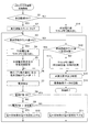
図2は、このような撮像装置1の機能的構成のうち、LEDストロボ撮影処理を実行するための機能的構成を示す機能ブロック図である。
FIG. 2 is a functional block diagram illustrating a functional configuration for executing the LED strobe photographing process among the functional configurations of the
LEDストロボ撮影処理とは、撮像部13の撮像動作と共に、ストロボ(LED部31)を発光させるまでの一連の処理であって、記録用の撮像動作の前段階に実行されるキャリブレーションを含む処理である。
キャリブレーションとは、LED部31の発光状態(電流IFの値)が所望の状態になるように、電圧印加部18によりLED部31に印加される電圧Voutの値を必要最小限の値に調整することをいう。これにより、LED部31を発光させるために必要となる電力効率が向上し、発光部17のEDLC部32の劣化を抑制することができる。
The LED strobe photographing process is a series of processing until the strobe (LED unit 31) emits light, together with the image capturing operation of the
Calibration refers to adjusting the value of the voltage Vout applied to the LED unit 31 by the
このようにキャリブレーションでは、発光状態検出部19による発光状態の検出が必要となる。このため、撮像動作時のストロボ発光とは別に、LED部31の発光が必要になる。本実施形態では、このようなLED部31の発光として、赤目軽減動作時のLED部31の発光が利用される。
ここで、赤目軽減動作とは、次のような動作をいう。即ち、暗部に存在する人物を、ストロボ発光をしながら撮影すると、当該人物の目の瞳孔は開いた状態であるため、網膜の毛細血管がストロボの光を反射させる。その瞬間の当該人物が撮影されるので、その撮影により得られた撮像画像においては、当該人物の目は、ストロボ光の反射のために赤目になる現象、即ちいわゆる赤目現象が生ずる。そこで、撮像装置(撮像装置1のみならず従来の撮像装置)は、ストロボ発光を伴う記録用の撮像動作時の前処理として、撮像動作とは独立して、ストロボ発光をする動作をすることで、当該人物の瞳孔を閉じさせて赤目現象を抑制する。このように、赤目現象を抑制する目的で、記録用の撮像動作時のストロボ発光の前に、ストロボ発光する動作が、赤目軽減動作である。
即ち、本実施形態では、このような赤目軽減動作と兼用して、キャリブレーションが実行される。
これにより、ユーザにキャリブレーションを意識させることなく、LED部31の電圧Voutの値の調整が適切に行われる。また、赤目軽減動作は、撮像部13の撮像動作とは独立した動作であるため、赤目軽減動作時のLED部31の発光、即ちキャリブレーションのためのLED部31の発光は、撮像画像に悪影響を与えることはない。また、キャリブレーションだけのために電力が供給されることもない。
Thus, in the calibration, it is necessary to detect the light emission state by the light emission
Here, the red-eye reduction operation refers to the following operation. That is, when a person existing in a dark part is photographed while performing strobe light emission, since the pupil of the person's eyes is in an open state, the capillaries of the retina reflect the light of the strobe. Since the person at that moment is photographed, in the captured image obtained by the photographing, a phenomenon that the person's eyes become red eyes due to reflection of strobe light, that is, a so-called red-eye phenomenon occurs. Therefore, the imaging apparatus (the conventional imaging apparatus as well as the imaging apparatus 1) performs an operation of emitting the strobe light independently of the imaging operation as a pre-processing at the time of the recording imaging operation with the strobe light emission. The pupil of the person is closed to suppress the red-eye phenomenon. As described above, for the purpose of suppressing the red-eye phenomenon, the operation for emitting the strobe light before the strobe light emission during the recording imaging operation is the red-eye reduction operation.
That is, in the present embodiment, calibration is executed in combination with such a red-eye reduction operation.
Thereby, the value of the voltage Vout of the LED unit 31 is appropriately adjusted without making the user aware of calibration. Further, since the red-eye reduction operation is an operation independent of the imaging operation of the
撮像装置1は、LEDストロボ撮影処理が実行される場合には、図2に示すように、制御部11において、操作検出部41と、モード設定部42と、ストロボ設定部43と、印加制御部44と、記憶制御部45と、撮像制御部46と、が機能する。
この場合、メモリデバイス12の一領域として、印加電圧データ記憶部51が設けられ、メモリカード25の一領域として、画像データ記録部52が設けられていることが例示であって、その他例えば、USBコネクタ23からケーブルを介して接続される外部機器等の記憶部の一領域に設けられるようにしてもよい。
When the LED strobe photographing process is executed, the
In this case, the application voltage
印加電圧データ記憶部51は、電圧印加部18によりLED部31に印加される電圧Voutの指令値のデータを記憶している。
画像データ記録部52は、撮像部により記録用として撮像された撮像画像のデータを記録する。
The applied voltage
The image
操作検出部41は、ユーザにより操作部に対してなされた操作の内容を検出する。具体的には、撮像装置1の動作モードの設定を指示する操作、LEDストロボ撮影処理の開始を指示する操作、撮像画像の記録を指示する操作等各種操作の内容が、操作検出部41により検出される。
The
モード設定部42は、操作検出部41の検出結果等に基づいて、撮像装置1の動作モードを設定する。本実施形態では、ストロボ発光を伴う撮像動作がなされる動作モードとして、赤目軽減動作を実行するモード(以下、「赤目軽減モード」と呼ぶ)と、当該赤目軽減動作を実行しない通常のモード(以下、「通常モード」と呼ぶ)とが存在する。
ストロボ設定部43は、LEDストロボ撮影処理において必要となる各種設定の処理等、LEDストロボ撮影処理における一般的な処理を実行する。具体的には、ストロボ設定部43は、キャリブレーションにおける発光回数のカウントやクリア等を実行する。
The
The
印加制御部44は、電圧印加部18による電圧の印加のタイミングや、印加量(即ち、電圧Voutの値)を制御する。
印加量の制御を具体的に説明すると、印加制御部44は、初期状態では、電圧Voutの指令値(適切と判断される値)として、初期状態では印加電圧データ記憶部51から前回の指令値を取得する。その後は、印加制御部44は、発光状態検出部により検出された発光部17の発光状態(本実施形態においては電流IFの値)をフィードバック値として、所望の発光状態を設定値(本実施形態においては電流IFの適切な値として設定された設定値)として、設定値に対するフィードバック値の誤差を算出する。そして、印加制御部44は、当該誤差に基づいて、電圧Voutの指令値(適切と判断される値)を取得する。
印加制御部44は、このようにして取得した電圧Voutの指令値(適切と判断される値)を電圧印加部18に通知して、当該指令値の電圧Voutを電圧印加部が出力するように制御する。
The
The control of the application amount will be described in detail. The
The
記憶制御部45は、このようにして印加制御部44により繰り返し行われるキャリブレーションの結果、即ち、逐次取得される電圧Voutの指令値(適切と判断される値)を印加電圧データ記憶部51に記憶させる制御を実行したり、記録用として得られた撮像画像のデータを画像データ記録部52に記録する制御を実行したりする。
撮像制御部46は、撮像部13の撮像動作を制御する。この際、撮像制御部46は、レンズ駆動部15も合わせて制御する。
The
The
図3は、図2の機能的構成を有する図1の撮像装置1が実行するLEDストロボ撮影処理の流れを説明するフローチャートである。
ユーザは、操作部21を用いて、LEDストロボ撮影処理の開始を指示する所定の操作をすることができる。
LEDストロボ撮影処理は、このようなユーザによる所定の操作が操作検出部41により検出されたことを契機として開始され、次のような処理が実行される。
FIG. 3 is a flowchart for explaining the flow of LED strobe photographing processing executed by the
The user can use the
The LED flash photographing process is started when such a predetermined operation by the user is detected by the
ステップS1において、モード設定部42は、赤目軽減モードに設定したか否かを判断する。
赤目軽減モードでない通常モードが設定されている場合(赤目軽減OFFの場合)、ステップS1においてNOであると判断されて、処理はステップS14に進む。ただし、ステップS14以降の処理は後述する。
赤目軽減モードに設定されている場合(赤目軽減ONの場合)には、ステップS1においてYESであると判断されて、処理はステップS2に進む。
In step S1, the
When the normal mode that is not the red-eye reduction mode is set (when the red-eye reduction is OFF), it is determined as NO in Step S1, and the process proceeds to Step S14. However, the process after step S14 is mentioned later.
When the red-eye reduction mode is set (when red-eye reduction is ON), it is determined as YES in Step S1, and the process proceeds to Step S2.
ステップS2において、ストロボ設定部43は、発光回数のカウントをクリアにする。即ち、ストロボ設定部43により、発光部17の発光回数は0回とされる。これにより、赤目軽減動作、及びそれと兼用にキャリブレーションが開始され、次のようなステップS3乃至S11のループ処理が繰り返し実行される。
In step S2, the
ステップS3において、ストロボ設定部43は、発光回数のカウントが0回か否かを判断する。
発光回数のカウントが0回以上である場合(発光回数カウント値>0の場合)には、ステップS3においてNOであると判断されて、処理はステップS12に進む。ただし、ステップS12以降の処理は後述する。
発光回数のカウントが0回である場合(発光回数カウント値=0の場合)には、ステップS4においてYESであると判断されて、処理はステップS4に進む。
In step S <b> 3, the
When the count of the number of times of light emission is 0 or more (when the number of times of light emission count> 0), it is determined as NO in step S3, and the process proceeds to step S12. However, the process after step S12 is mentioned later.
When the number of times of light emission is 0 (when the number of times of light emission count = 0), it is determined as YES in step S4, and the process proceeds to step S4.
ステップS4において、印加制御部44は、印加電圧値のラストメモリを読み出す。ここで、印加電圧値とは、電圧Voutの指令値(適切と判断される値)を意味する。従って、印加電圧値のラストメモリとは、前回のキャリブレーション時に、次回に印加電圧値として使用すべきとして設定されて(前回における、後述するステップS8乃至S11の処理が実行されて)、印加電圧データ記憶部51に記憶されている電圧Voutの指令値(適切と判断される値)を意味する。
In step S4, the
ステップS5において、印加制御部44は、印加電圧値を設定し、定電流値を設定する。即ち、印加制御部44は、電圧印加部18による発光部17への印加をステップS4の処理で読み出した印加電圧値で行うように設定する。また、印加制御部44は、電圧印加部18に対して、発光部17が所定の定電流値となるように設定する。
In step S5, the
ステップS6において、印加制御部44は、発光(プリ発光動作)を実行し、ストロボ設定部43は、発光回数カウント値+1とする。
即ち、印加制御部44は、赤目軽減用兼キャリブレーション用に、撮像部13での撮像を行う時の発光(本発光動作)の前の発光動作であるプリ発光動作を行うような電圧印加部18への制御を実行する。その結果、発光部17が発光する。
また、発光部17の発光に伴って、ストロボ設定部43は、発光回数をカウントする。その結果、発光回数カウント値が1回となる。
In step S6, the
That is, the
As the
ステップS7において、発光状態検出部19は、電流を検出する。詳細には、発光状態検出部19は、発光部17の発光時の電流IF値を検出する。その後、発光状態検出部19は、検出した電流IF値を印加制御部44に供給する。
In step S7, the light emission
ステップS8において、印加制御部44は、電流IF値がOKか否かを判断する。詳細には、印加制御部44は、ステップS7において検出された電流IF値と、印加電圧データ記憶部51に記憶されているデータ値とを比較して、発光部17の電流IFの値が適切な値であるか否かを判断する。
発光部17の電流IF値が適切であると判断された場合(電流IF値=OKの場合)には、ステップS8においてYESと判断されて、処理はステップS3に戻り、再びステップS3以降の処理が実行される。
これに対して、発光部17の電流IF値が適切でないと判断された場合(電流IF値=NGの場合)には、ステップS8においてNOと判断されて、処理はステップS9に進む。
In step S8, the
If it is determined that the current IF value of the
On the other hand, when it is determined that the current IF value of the
ステップS9において、印加制御部44は、電流IF値を設定値が超えているか否かを判断する。印加制御部44は、ステップS7の処理において検出された電流IF値と、印加電圧データ記憶部51に記憶されている設定値とを比較して、ステップS7の処理において検出された電流IF値が設定値よりも高いか否かを判断する。
検出された電流IF値よりも設定値が高いと判断された場合(電流IF値<設定値の場合)には、ステップS9においてYESであり、処理はステップS10に進む。
In step S9, the
If it is determined that the set value is higher than the detected current IF value (if current IF value <set value), YES is determined in step S9, and the process proceeds to step S10.
ステップS10において、印加制御部44は、電圧印加部18の電圧設定を上げる。これにより、その後、発光があった場合には、設定されている電圧値は、適正な値に近づいた値になる。その後処理はステップS3に戻り、再びステップS3以降の処理が実行される。
In step S <b> 10, the
これに対して、検出された電流IF値が設定値以上であると判断された場合(電流IF値≧設定値の場合)には、ステップS9においてNOであり、処理はステップS11に進む。 On the other hand, when it is determined that the detected current IF value is equal to or larger than the set value (when current IF value ≧ set value), NO is determined in step S9, and the process proceeds to step S11.
ステップS11において、印加制御部44は、電圧印加部18の電圧設定を下げる。これにより、その後、発光があった場合には、設定されている電圧値は、適正な値に近づいた値になる。その後処理はステップS3に戻り、再びステップS3以降の処理が実行される。
In step S <b> 11, the
ステップS12において、ストロボ設定部43は、発光回数カウント値よりも赤目現象を軽減させるため必要とされる、予め設定された回数(以降、設定回数という)の方が多い否かを判断する。
発光回数カウント値よりも設定回数の方が多いと判断された場合(発光回数カウント値<設定回数)には、ステップS12においてYESと判断されて、処理はステップS6に進む。
これに対して、発光回数カウント値が設定回数以上であると判断された場合(発光回数カウント値≧設定回数)には、ステップS12においてNOと判断されて、処理はステップS13に進む。
In step S <b> 12, the
If it is determined that the set number of times is larger than the light emission number count value (light emission number count value <set number of times), YES is determined in step S12, and the process proceeds to step S6.
On the other hand, when it is determined that the light emission count value is greater than or equal to the set number (light emission count value ≧ set number), NO is determined in step S12, and the process proceeds to step S13.
ステップS13において、印加制御部44は、ラストメモリを実行し、記憶制御部45は、電圧印加部18の電圧値とラストメモリ実行時の電圧値と日時を、印加電圧データ記憶部51に記憶する制御を実行する。その後、処理は、ステップS15に進む。ただし、ステップS15以降の処理は後述する。
In step S <b> 13, the
ステップS14において、印加制御部44は、印加電圧値のラストメモリ読み出しを行う。即ち、印加制御部44は、印加電圧データ記憶部51から前回の発光で用いた値として記憶される印加電圧値を読み出す。
In step S14, the
ステップS15において、印加制御部44は、本発光動作を実行する。即ち、印加制御部44は、撮像部13での撮像を行う時の発光(本発光動作)の発光動作を行うような電圧印加部18への制御を実行する。その結果、発光部17が発光する。また、発光部17の発光に伴って、撮像制御部46は、撮像部13を制御する。
ステップS15において、発光部17での発光が行われる時には、発光部17の電圧はすでに調整されているために、過剰な電圧での発光が行われなくなる。
In step S15, the
In step S15, when the
ステップS16において、記憶制御部45は、撮像画像のデータを記録する。記憶制御部45は、撮像画像のデータを画像データ記録部52に記憶する制御を実行する。その後、LEDストロボ撮影処理は終了する。
In step S <b> 16, the
以上のように構成される撮像装置1は、発光部17と、撮像部13と、操作検出部41と、電圧印加部18と、印加制御部44と、記憶制御部45とを備える。
発光部17は、電圧が印加されることにより発光する。
撮像部13は、画像を撮像する。
操作検出部41は、撮像部13の撮像対象の画像のデータの記録指示を検出する。
電圧印加部18は、操作検出部41によって記録指示が検出されると、発光部17に発光させるべく電圧を印加する。
印加制御部44は、電圧印加部18によって電圧が印加されて発光部17が発光すると、この時の発光状態から発光部17の劣化を引き起こさない程度の印加電圧値を取得する。また、印加制御部44は、取得された印加電圧値の電圧を、発光部17に印加するように電圧印加部18を制御する。
記憶制御部45は、発光部17が発光した時に撮像部13が撮像した画像のデータを所定のメモリカード25に記録するように制御する。
The
The
The
The
The
When a voltage is applied by the
The
従って、撮像装置1は、操作検出部41によって記録指示が検出されると、発光部17を発光させるべく電圧を印加し、印加制御部44によって取得した印加電圧値を発光部17に印加し、電圧印加部18によって電圧が印加された発光部17が発光すると、この時の発光状態から適切と判断された印加電圧値を取得し、取得された印加電圧値の電圧を、電圧印加部18が発光部17に印加するように制御する。
このため、撮像装置1は、例えば、発光部17に過剰な電圧をかけることがなく、発光部17の劣化を確実に防止することができる。また、撮像装置1は、例えば、発光部17で過剰な電圧をかけず、結果的に電源24の寿命を延ばすことができる。
Therefore, when the recording instruction is detected by the
For this reason, the
また、撮像装置1は、発光部17へ電圧を印加するための電力を含め、撮像装置1が使用する電力は、所定の電源により供給されるようにし、適切な印加電圧値を電源24の劣化を引き起こさない程度の電圧値とすることができる。
このように構成した場合には、撮像装置1は、電源24の劣化を引き起こすことがないために、電源24の寿命を延ばすことができる。
なお、上述した発光部17や電源24等の劣化を引き起こさない程度の電圧値とは、実測により、又は所定の劣化予測式により演算されて、メモリデバイス12やメモリカード25等のメモリに予め記憶されている。従って、劣化を引き起こさない程度の電圧値と検出した値との対比を行って、電圧値を調整することにより発光部17や電源24等の劣化を引き起こさない程度の電圧下での使用が可能となる。
In addition, the
When configured in this manner, the
Note that the above-described voltage value that does not cause deterioration of the
また、印加制御部44が適切な印加電圧値を取得するために用いた発光状態が取得された発光とは、赤目軽減用の発光である。
従って、撮像装置1は、赤目軽減用の発光を利用して、電圧値を取得することができるために、別途、電圧値を取得するための発光操作を設ける必要がない。
Further, the light emission for which the light emission state used for the
Therefore, since the
なお、本発明は、上述の実施形態に限定されるものではなく、本発明の目的を達成できる範囲での変形、改良等は本発明に含まれるものである。 In addition, this invention is not limited to the above-mentioned embodiment, The deformation | transformation in the range which can achieve the objective of this invention, improvement, etc. are included in this invention.
上述の実施形態では、赤目軽減モードが設定されていることで赤目軽減に係る処理が実行されるように構成されていたがこれに限られず、例えば、赤目軽減モードが設定されていなくても被写体として顔を認識した場合に赤目軽減に係る処理を実行するように構成してもよい。 In the above-described embodiment, the red-eye reduction mode is set so that the processing related to red-eye reduction is executed. However, the present invention is not limited to this. For example, the subject can be processed even if the red-eye reduction mode is not set. When the face is recognized, the processing relating to red-eye reduction may be executed.
また、上述の実施形態では、発光部17の発光時の光度の度合いを導き出すためのパラメータとして、電流IFを用いていたがこれに限られない。光度の度合いを導き出すためのパラメータとしては、例えば、電流IFと正の関係となる電圧VFを用いることもできる。即ち、電圧VFを検出して、電圧VFと電流IFとの関係から、電流IFを算出することで、光度の度合いを導き出すことができる。また、電圧VFと負の関係となる温度Tを用いることもできる。即ち、温度Tを検出して、温度Tと電圧VFとの関係から、電圧VFを算出し、さらに、電圧VFと電流IFの関係から、電流IFを算出することで、光度の度合いを導き出すことができる。
In the above-described embodiment, the current IF is used as a parameter for deriving the degree of luminous intensity at the time of light emission of the
また、上述の実施形態では、発光部17を構成する一例としてLEDにより説明を行ったがこれに限られない。発光部17は、発光ダイオードであればよく、例えば、有機EL(electroluminescence)等の発光ダイオードであってもよい。
Moreover, in the above-mentioned embodiment, although demonstrated by LED as an example which comprises the
また、上述の実施形態では、本発明が適用される撮像装置1は、デジタルカメラを例として説明したが、特にこれに限定されない。
例えば、本発明は、LEDストロボ撮影機能を有する電子機器一般に適用することができる。具体的には、例えば、本発明は、ノート型のパーソナルコンピュータ、テレビジョン受像機、ビデオカメラ、携帯型ナビゲーション装置、携帯電話機、ポータブルゲーム機等に適用可能である。
In the above-described embodiment, the
For example, the present invention can be applied to general electronic devices having an LED flash photographing function. Specifically, for example, the present invention can be applied to a notebook personal computer, a television receiver, a video camera, a portable navigation device, a mobile phone, a portable game machine, and the like.
上述した一連の処理は、ハードウェアにより実行させることもできるし、ソフトウェアにより実行させることもできる。
換言すると、図2の機能的構成は例示に過ぎず、特に限定されない。即ち、上述した一連の処理を全体として実行できる機能が撮像装置1に備えられていれば足り、この機能を実現するためにどのような機能ブロックを用いるのかは特に図2の例に限定されない。
また、1つの機能ブロックは、ハードウェア単体で構成してもよいし、ソフトウェア単体で構成してもよいし、それらの組み合わせで構成してもよい。
The series of processes described above can be executed by hardware or can be executed by software.
In other words, the functional configuration of FIG. 2 is merely an example and is not particularly limited. That is, it is sufficient that the
In addition, one functional block may be constituted by hardware alone, software alone, or a combination thereof.
一連の処理をソフトウェアにより実行させる場合には、そのソフトウェアを構成するプログラムが、コンピュータ等にネットワークや記録媒体からインストールされる。
コンピュータは、専用のハードウェアに組み込まれているコンピュータであってもよい。また、コンピュータは、各種のプログラムをインストールすることで、各種の機能を実行することが可能なコンピュータ、例えば汎用のパーソナルコンピュータであってもよい。
When a series of processing is executed by software, a program constituting the software is installed on a computer or the like from a network or a recording medium.
The computer may be a computer incorporated in dedicated hardware. The computer may be a computer capable of executing various functions by installing various programs, for example, a general-purpose personal computer.
このようなプログラムを含む記録媒体は、ユーザにプログラムを提供するために装置本体とは別に配布される図1のメモリデバイス12により構成されるだけでなく、装置本体に予め組み込まれた状態でユーザに提供される記録媒体等で構成される。メモリカード25は、例えば、磁気ディスク(フロッピディスクを含む)、光ディスク、又は光磁気ディスク等により構成される。光ディスクは、例えば、CD−ROM(Compact Disk−Read Only Memory),DVD(Digital Versatile Disk)等により構成される。光磁気ディスクは、MD(Mini−Disk)等により構成される。また、装置本体に予め組み込まれた状態でユーザに提供される記録媒体は、例えば、プログラムが記録されている図1のメモリデバイス12や、図1のUSBコネクタ23にケーブルを介して接続されるハードディスク等で構成される。
The recording medium including such a program is not only constituted by the
なお、本明細書において、記録媒体に記録されるプログラムを記述するステップは、その順序に沿って時系列的に行われる処理はもちろん、必ずしも時系列的に処理されなくとも、並列的或いは個別に実行される処理をも含むものである。 In the present specification, the step of describing the program recorded on the recording medium is not limited to the processing performed in time series along the order, but is not necessarily performed in time series, either in parallel or individually. The process to be executed is also included.
以上、本発明のいくつかの実施形態について説明したが、これらの実施形態は、例示に過ぎず、本発明の技術的範囲を限定するものではない。本発明はその他の様々な実施形態を取ることが可能であり、さらに、本発明の要旨を逸脱しない範囲で、省略や置換等種々の変更を行うことができる。これら実施形態やその変形は、本明細書等に記載された発明の範囲や要旨に含まれると共に、特許請求の範囲に記載された発明とその均等の範囲に含まれる。 As mentioned above, although several embodiment of this invention was described, these embodiment is only an illustration and does not limit the technical scope of this invention. The present invention can take other various embodiments, and various modifications such as omission and replacement can be made without departing from the gist of the present invention. These embodiments and modifications thereof are included in the scope and gist of the invention described in this specification and the like, and are included in the invention described in the claims and the equivalents thereof.
以下に、本願の出願当初の特許請求の範囲に記載された発明を付記する。
[付記1]
電圧が印加されることにより発光する発光手段と、
画像を撮像する撮像手段と、
前記撮像手段の撮像対象の画像のデータの記録指示を検出する検出手段と、
前記検出手段によって記録指示が検出されると、前記発光手段に電圧を印加する電圧印加手段と、
前記電圧印加手段によって電圧が印加されて前記発光手段が発光すると、この時の発光状態から前記発光手段の劣化を引き起こさない程度の印加電圧値を取得する取得手段と、
前記取得手段によって取得された印加電圧値の電圧を前記発光手段に印加するよう前記電圧印加手段を制御する電圧印加制御手段と、
前記発光手段が発光した時に前記撮像手段が撮像した画像のデータを所定の記録媒体に記録するように制御する記録制御手段と、
を備えたことを特徴とする撮像装置。
[付記2]
前記発光手段へ電圧を印加するための電力を含め、前記撮像装置が使用する電力は、所定の電源により供給されることを特徴とする付記1に記載の撮像装置。
[付記3]
前記取得手段が適切な印加電圧値を取得するために用いた発光状態が取得された発光とは、赤目軽減用の発光であることを特徴とする付記1又は2に記載の撮像装置。
[付記4]
前記発光手段は、発光ダイオードであることを特徴とする付記1乃至3の何れか1つに記載の撮像装置。
[付記5]
電圧が印加されることにより発光する発光手段と、画像を撮像する撮像手段と、を備える撮像装置が実行する照明制御方法であって、
前記撮像手段の撮像対象の画像のデータの記録指示を検出する検出ステップと、
前記検出ステップによって記録指示が検出されると、前記発光手段を発光させるべく電圧を印加する電圧印加ステップと、
前記電圧印加ステップによって電圧が印加されて前記発光手段が発光すると、この時の発光状態から前記発光手段の劣化を引き起こさない程度の印加電圧値を取得する取得ステップと、
前記取得ステップによって取得された印加電圧値の電圧を前記発光手段に印加するよう制御する電圧印加制御ステップと、
前記発光手段が発光した時に前記撮像手段が撮像した画像のデータを所定の記録媒体に記録するように制御する記録制御ステップと、
を含むことを特徴とする照明制御方法。
[付記6]
電圧が印加されることにより発光する発光手段と、画像を撮像する撮像手段と、を備える撮像装置を制御するコンピュータを、
前記撮像手段の撮像対象の画像のデータの記録指示を検出する検出手段、
前記検出手段によって記録指示が検出されると、前記発光手段を発光させるべく電圧を印加する電圧印加手段、
前記電圧印加手段によって電圧が印加されて前記発光手段が発光すると、この時の発光状態から前記発光手段の劣化を引き起こさない程度の印加電圧値を取得する取得手段、
前記取得手段によって取得された印加電圧値の電圧を前記発光手段に印加するように前記電圧印加手段を制御する電圧印加制御手段、
前記発光手段が発光した時に前記撮像手段が撮像した画像のデータを所定の記録媒体に記録するように制御する記録制御手段、
として機能させることを特徴とするプログラム。
The invention described in the scope of claims at the beginning of the filing of the present application will be appended.
[Appendix 1]
A light emitting means that emits light when a voltage is applied;
An imaging means for capturing an image;
Detecting means for detecting an instruction to record data of an image to be imaged by the imaging means;
A voltage applying means for applying a voltage to the light emitting means when a recording instruction is detected by the detecting means;
When the voltage is applied by the voltage applying unit and the light emitting unit emits light, the obtaining unit acquires an applied voltage value that does not cause deterioration of the light emitting unit from the light emitting state at this time;
Voltage application control means for controlling the voltage application means to apply a voltage of the applied voltage value acquired by the acquisition means to the light emitting means;
Recording control means for controlling the image data captured by the imaging means to be recorded on a predetermined recording medium when the light emitting means emits light;
An imaging apparatus comprising:
[Appendix 2]
The imaging apparatus according to
[Appendix 3]
The imaging apparatus according to
[Appendix 4]
The imaging device according to any one of
[Appendix 5]
An illumination control method executed by an imaging apparatus comprising: a light emitting unit that emits light when a voltage is applied; and an imaging unit that captures an image,
A detection step of detecting an instruction to record data of an image to be imaged by the imaging means;
A voltage applying step of applying a voltage to cause the light emitting means to emit light when a recording instruction is detected by the detecting step;
When a voltage is applied by the voltage application step and the light emitting means emits light, an acquisition step of acquiring an applied voltage value that does not cause deterioration of the light emitting means from the light emitting state at this time;
A voltage application control step for controlling the voltage of the applied voltage value acquired by the acquiring step to be applied to the light emitting means;
A recording control step for controlling to record data of an image captured by the imaging unit on a predetermined recording medium when the light emitting unit emits light;
The lighting control method characterized by including.
[Appendix 6]
A computer that controls an imaging device including: a light emitting unit that emits light when a voltage is applied; and an imaging unit that captures an image.
Detecting means for detecting an instruction to record data of an image to be imaged by the imaging means;
A voltage applying means for applying a voltage to cause the light emitting means to emit light when a recording instruction is detected by the detecting means;
When the voltage is applied by the voltage applying means and the light emitting means emits light, the obtaining means acquires an applied voltage value that does not cause deterioration of the light emitting means from the light emitting state at this time;
Voltage application control means for controlling the voltage application means to apply the voltage of the applied voltage value acquired by the acquisition means to the light emitting means;
Recording control means for controlling the image data captured by the imaging means to be recorded on a predetermined recording medium when the light emitting means emits light;
A program characterized by functioning as
1・・・撮像装置,11・・・制御部,12・・・メモリデバイス,13・・・撮像部,14・・・A/D変換部,15・・・レンズ駆動部,16・・・駆動機構,17・・・発光部,18・・・電圧印加部,19・・・発光状態検出部,20・・・表示部,21・・・操作部,22・・・メモリカード装着部,23・・・USBコネクタ,24・・・電源,25・・・メモリカード,41・・・操作検出部,42・・・モード設定部,43・・・ストロボ設定部,44・・・印加制御部,45・・・記憶制御部,46・・・撮像制御部,51・・・印加電圧データ記憶部,52・・・画像データ記録部
DESCRIPTION OF
Claims (7)
画像を撮像する撮像手段と、
前記発光手段に電圧を印加する電圧印加手段と、
前記電圧印加手段によって電圧が印加されて前記発光手段が発光すると、この時の発光状態に対応する印加電圧値とこれ以前に発光した所望の発光状態に対応する印加電圧値との誤差に基づいて、今回の撮像における印加電圧値を取得する取得手段と、
前記取得手段によって取得された印加電圧値の電圧を前記発光手段に印加するよう前記電圧印加手段を制御する電圧印加制御手段と、
前記電圧印加制御手段による制御により発光手段が発光した時に前記撮像手段が撮像した画像のデータを所定の記録媒体に記録するように制御する記録制御手段と、
を備えたことを特徴とする撮像装置。 A light emitting means that emits light when a voltage is applied;
An imaging means for capturing an image;
Voltage applying means for applying a voltage to the light emitting means;
When a voltage is applied by the voltage applying unit and the light emitting unit emits light , based on an error between an applied voltage value corresponding to the light emitting state at this time and an applied voltage value corresponding to a desired light emitting state previously emitted. Acquiring means for acquiring an applied voltage value in the current imaging;
Voltage application control means for controlling the voltage application means to apply a voltage of the applied voltage value acquired by the acquisition means to the light emitting means;
Recording control means for controlling the image data picked up by the imaging means to be recorded on a predetermined recording medium when the light emitting means emits light under the control of the voltage application control means;
An imaging apparatus comprising:
前記電圧印加手段は、前記検出手段によって記録指示が検出されると、前記発光手段に
電圧を印加することを特徴とする請求項1乃至4の何れかに記載の撮像装置。 A detection unit for detecting an instruction to record data of an image to be imaged by the imaging unit;
The imaging apparatus according to claim 1, wherein the voltage application unit applies a voltage to the light emitting unit when a recording instruction is detected by the detection unit.
前記発光手段を発光させるべく電圧を印加する電圧印加ステップと、
前記電圧印加ステップによって電圧が印加されて前記発光手段が発光すると、前記電圧印加ステップにて電圧が印加されて前記発光手段が発光すると、この時の発光状態に対応する印加電圧値とこれ以前に発光した所望の発光状態に対応する印加電圧値との誤差に基づいて、今回の撮像における印加電圧値を取得する取得ステップと、
前記取得ステップによって取得された印加電圧値の電圧を前記発光手段に印加するよう制御する電圧印加制御ステップと、
前記発光手段が発光した時に前記撮像手段が撮像した画像のデータを所定の記録媒体に記録するように制御する記録制御ステップと、
を含むことを特徴とする照明制御方法。 An illumination control method executed by an imaging apparatus comprising: a light emitting unit that emits light when a voltage is applied; and an imaging unit that captures an image,
A voltage applying step for applying a voltage to cause the light emitting means to emit light;
When a voltage is applied by the voltage applying step and the light emitting means emits light, when a voltage is applied in the voltage applying step and the light emitting means emits light, the applied voltage value corresponding to the light emitting state at this time and the previous An acquisition step of acquiring an applied voltage value in the current imaging based on an error from an applied voltage value corresponding to a desired emission state of light emission ;
A voltage application control step for controlling the voltage of the applied voltage value acquired by the acquiring step to be applied to the light emitting means;
A recording control step for controlling to record data of an image captured by the imaging unit on a predetermined recording medium when the light emitting unit emits light;
The lighting control method characterized by including.
前記発光手段を発光させるべく電圧を印加する電圧印加手段、
前記電圧印加手段によって電圧が印加されて前記発光手段が発光すると、この時の発光状態に対応する印加電圧値とこれ以前に発光した所望の発光状態に対応する印加電圧値との誤差に基づいて、今回の撮像における印加電圧値を取得する取得手段、
前記取得手段によって取得された印加電圧値の電圧を前記発光手段に印加するように前記電圧印加手段を制御する電圧印加制御手段、
前記発光手段が発光した時に前記撮像手段が撮像した画像のデータを所定の記録媒体に記録するように制御する記録制御手段、
として機能させることを特徴とするプログラム。 A computer that controls an imaging device including: a light emitting unit that emits light when a voltage is applied; and an imaging unit that captures an image.
Voltage applying means for applying a voltage to cause the light emitting means to emit light,
When a voltage is applied by the voltage applying unit and the light emitting unit emits light , based on an error between an applied voltage value corresponding to the light emitting state at this time and an applied voltage value corresponding to a desired light emitting state previously emitted. , Acquisition means for acquiring an applied voltage value in the current imaging,
Voltage application control means for controlling the voltage application means to apply the voltage of the applied voltage value acquired by the acquisition means to the light emitting means;
Recording control means for controlling the image data captured by the imaging means to be recorded on a predetermined recording medium when the light emitting means emits light;
A program characterized by functioning as
Priority Applications (1)
| Application Number | Priority Date | Filing Date | Title |
|---|---|---|---|
| JP2012061878A JP6232690B2 (en) | 2012-03-19 | 2012-03-19 | Imaging apparatus, illumination control method, and program |
Applications Claiming Priority (1)
| Application Number | Priority Date | Filing Date | Title |
|---|---|---|---|
| JP2012061878A JP6232690B2 (en) | 2012-03-19 | 2012-03-19 | Imaging apparatus, illumination control method, and program |
Publications (3)
| Publication Number | Publication Date |
|---|---|
| JP2013195644A JP2013195644A (en) | 2013-09-30 |
| JP2013195644A5 JP2013195644A5 (en) | 2015-04-30 |
| JP6232690B2 true JP6232690B2 (en) | 2017-11-22 |
Family
ID=49394673
Family Applications (1)
| Application Number | Title | Priority Date | Filing Date |
|---|---|---|---|
| JP2012061878A Expired - Fee Related JP6232690B2 (en) | 2012-03-19 | 2012-03-19 | Imaging apparatus, illumination control method, and program |
Country Status (1)
| Country | Link |
|---|---|
| JP (1) | JP6232690B2 (en) |
Families Citing this family (2)
| Publication number | Priority date | Publication date | Assignee | Title |
|---|---|---|---|---|
| DE102018119182C5 (en) * | 2018-08-07 | 2021-10-14 | Basler Ag | Device and method for controlling the lighting in industrial camera systems |
| JP7204530B2 (en) * | 2019-02-28 | 2023-01-16 | キヤノン株式会社 | Lighting device and its control method |
Family Cites Families (6)
| Publication number | Priority date | Publication date | Assignee | Title |
|---|---|---|---|---|
| JP2003140236A (en) * | 2001-11-05 | 2003-05-14 | Fuji Photo Film Co Ltd | Camera |
| JP4228277B2 (en) * | 2003-01-31 | 2009-02-25 | 富士フイルム株式会社 | LED lighting device |
| JP2005303233A (en) * | 2004-04-16 | 2005-10-27 | Nsk Ltd | Illumination light source device |
| JP2007165411A (en) * | 2005-12-09 | 2007-06-28 | Matsushita Electric Ind Co Ltd | Semiconductor light emitting device and light emission control method thereof |
| JP5024061B2 (en) * | 2008-01-10 | 2012-09-12 | 株式会社ニコン | Image capturing apparatus and display device control method |
| JP5625370B2 (en) * | 2010-01-29 | 2014-11-19 | オムロン株式会社 | Lighting control device and lighting device including the same |
-
2012
- 2012-03-19 JP JP2012061878A patent/JP6232690B2/en not_active Expired - Fee Related
Also Published As
| Publication number | Publication date |
|---|---|
| JP2013195644A (en) | 2013-09-30 |
Similar Documents
| Publication | Publication Date | Title |
|---|---|---|
| US8970716B2 (en) | Image-capturing apparatus and control method of the image-capturing apparatus | |
| US8319856B2 (en) | Imaging apparatus for calculating a histogram to adjust color balance | |
| US10200630B2 (en) | Image capturing apparatus capable of changing an aperture value based on a change in an aperture diameter, controlling method of the same, and recording medium | |
| JP2005184508A (en) | Imaging apparatus and control method thereof | |
| US9560286B2 (en) | Image capturing apparatus and method for controlling the same | |
| US10348977B2 (en) | Image pickup apparatus calculating light-amount variation characteristic of light from object, control method therefor, and storage medium storing control program therefor | |
| JP6232690B2 (en) | Imaging apparatus, illumination control method, and program | |
| JP6410416B2 (en) | IMAGING DEVICE AND IMAGING DEVICE CONTROL METHOD | |
| JP5045474B2 (en) | Electronic camera and electronic camera strobe device | |
| JP6335497B2 (en) | Imaging device, control method thereof, and control program | |
| JP5387645B2 (en) | Imaging apparatus and program thereof | |
| JP2011040799A (en) | Imaging device | |
| JP2011061640A (en) | Imaging apparatus | |
| JP2005115161A (en) | Electronic flash device, control method for electronic flash device and camera system | |
| US10284783B2 (en) | Imaging apparatus and control method of imaging apparatus | |
| JP4540374B2 (en) | Camera device provided with strobe lamp and imaging method of the camera device | |
| JP2005115160A (en) | Electronic flash device, control method for electronic flash device, camera and camera system | |
| JP4915272B2 (en) | Imaging apparatus and program thereof | |
| US20130251356A1 (en) | Imaging device | |
| JP5228428B2 (en) | Flash device, charging control program, and charging method | |
| JP5387639B2 (en) | Imaging apparatus and program thereof | |
| JP2024169975A (en) | Imaging device, control method thereof, and program | |
| JP2025128695A (en) | Illumination device, imaging system, and control method thereof | |
| JP4619020B2 (en) | Electronic equipment with strobe device | |
| JP6349625B2 (en) | Image recording apparatus and method |
Legal Events
| Date | Code | Title | Description |
|---|---|---|---|
| A521 | Request for written amendment filed |
Free format text: JAPANESE INTERMEDIATE CODE: A523 Effective date: 20150313 |
|
| A621 | Written request for application examination |
Free format text: JAPANESE INTERMEDIATE CODE: A621 Effective date: 20150313 |
|
| A977 | Report on retrieval |
Free format text: JAPANESE INTERMEDIATE CODE: A971007 Effective date: 20160120 |
|
| A131 | Notification of reasons for refusal |
Free format text: JAPANESE INTERMEDIATE CODE: A131 Effective date: 20160126 |
|
| A521 | Request for written amendment filed |
Free format text: JAPANESE INTERMEDIATE CODE: A523 Effective date: 20160325 |
|
| A131 | Notification of reasons for refusal |
Free format text: JAPANESE INTERMEDIATE CODE: A131 Effective date: 20160830 |
|
| A521 | Request for written amendment filed |
Free format text: JAPANESE INTERMEDIATE CODE: A523 Effective date: 20161027 |
|
| A02 | Decision of refusal |
Free format text: JAPANESE INTERMEDIATE CODE: A02 Effective date: 20170404 |
|
| A521 | Request for written amendment filed |
Free format text: JAPANESE INTERMEDIATE CODE: A523 Effective date: 20170703 |
|
| A911 | Transfer to examiner for re-examination before appeal (zenchi) |
Free format text: JAPANESE INTERMEDIATE CODE: A911 Effective date: 20170710 |
|
| TRDD | Decision of grant or rejection written | ||
| A01 | Written decision to grant a patent or to grant a registration (utility model) |
Free format text: JAPANESE INTERMEDIATE CODE: A01 Effective date: 20170926 |
|
| A61 | First payment of annual fees (during grant procedure) |
Free format text: JAPANESE INTERMEDIATE CODE: A61 Effective date: 20171009 |
|
| R150 | Certificate of patent or registration of utility model |
Ref document number: 6232690 Country of ref document: JP Free format text: JAPANESE INTERMEDIATE CODE: R150 |
|
| LAPS | Cancellation because of no payment of annual fees |