JP5923334B2 - Semiconductor device - Google Patents
Semiconductor device Download PDFInfo
- Publication number
- JP5923334B2 JP5923334B2 JP2012036511A JP2012036511A JP5923334B2 JP 5923334 B2 JP5923334 B2 JP 5923334B2 JP 2012036511 A JP2012036511 A JP 2012036511A JP 2012036511 A JP2012036511 A JP 2012036511A JP 5923334 B2 JP5923334 B2 JP 5923334B2
- Authority
- JP
- Japan
- Prior art keywords
- conductive layer
- insulating film
- contact
- semiconductor device
- layer
- Prior art date
- Legal status (The legal status is an assumption and is not a legal conclusion. Google has not performed a legal analysis and makes no representation as to the accuracy of the status listed.)
- Expired - Fee Related
Links
Images


Classifications
-
- H—ELECTRICITY
- H10—SEMICONDUCTOR DEVICES; ELECTRIC SOLID-STATE DEVICES NOT OTHERWISE PROVIDED FOR
- H10W—GENERIC PACKAGES, INTERCONNECTIONS, CONNECTORS OR OTHER CONSTRUCTIONAL DETAILS OF DEVICES COVERED BY CLASS H10
- H10W20/00—Interconnections in chips, wafers or substrates
- H10W20/01—Manufacture or treatment
- H10W20/031—Manufacture or treatment of conductive parts of the interconnections
- H10W20/067—Manufacture or treatment of conductive parts of the interconnections by modifying the pattern of conductive parts
-
- H—ELECTRICITY
- H10—SEMICONDUCTOR DEVICES; ELECTRIC SOLID-STATE DEVICES NOT OTHERWISE PROVIDED FOR
- H10B—ELECTRONIC MEMORY DEVICES
- H10B10/00—Static random access memory [SRAM] devices
- H10B10/12—Static random access memory [SRAM] devices comprising a MOSFET load element
- H10B10/125—Static random access memory [SRAM] devices comprising a MOSFET load element the MOSFET being a thin film transistor [TFT]
-
- H—ELECTRICITY
- H10—SEMICONDUCTOR DEVICES; ELECTRIC SOLID-STATE DEVICES NOT OTHERWISE PROVIDED FOR
- H10B—ELECTRONIC MEMORY DEVICES
- H10B10/00—Static random access memory [SRAM] devices
- H10B10/18—Peripheral circuit regions
-
- H—ELECTRICITY
- H10—SEMICONDUCTOR DEVICES; ELECTRIC SOLID-STATE DEVICES NOT OTHERWISE PROVIDED FOR
- H10W—GENERIC PACKAGES, INTERCONNECTIONS, CONNECTORS OR OTHER CONSTRUCTIONAL DETAILS OF DEVICES COVERED BY CLASS H10
- H10W20/00—Interconnections in chips, wafers or substrates
- H10W20/01—Manufacture or treatment
- H10W20/031—Manufacture or treatment of conductive parts of the interconnections
- H10W20/056—Manufacture or treatment of conductive parts of the interconnections by filling conductive material into holes, grooves or trenches
-
- H—ELECTRICITY
- H10—SEMICONDUCTOR DEVICES; ELECTRIC SOLID-STATE DEVICES NOT OTHERWISE PROVIDED FOR
- H10W—GENERIC PACKAGES, INTERCONNECTIONS, CONNECTORS OR OTHER CONSTRUCTIONAL DETAILS OF DEVICES COVERED BY CLASS H10
- H10W20/00—Interconnections in chips, wafers or substrates
- H10W20/01—Manufacture or treatment
- H10W20/071—Manufacture or treatment of dielectric parts thereof
- H10W20/081—Manufacture or treatment of dielectric parts thereof by forming openings in the dielectric parts
- H10W20/083—Manufacture or treatment of dielectric parts thereof by forming openings in the dielectric parts the openings being via holes penetrating underlying conductors
-
- H—ELECTRICITY
- H10—SEMICONDUCTOR DEVICES; ELECTRIC SOLID-STATE DEVICES NOT OTHERWISE PROVIDED FOR
- H10W—GENERIC PACKAGES, INTERCONNECTIONS, CONNECTORS OR OTHER CONSTRUCTIONAL DETAILS OF DEVICES COVERED BY CLASS H10
- H10W20/00—Interconnections in chips, wafers or substrates
- H10W20/40—Interconnections external to wafers or substrates, e.g. back-end-of-line [BEOL] metallisations or vias connecting to gate electrodes
- H10W20/41—Interconnections external to wafers or substrates, e.g. back-end-of-line [BEOL] metallisations or vias connecting to gate electrodes characterised by their conductive parts
- H10W20/42—Vias, e.g. via plugs
-
- H—ELECTRICITY
- H10—SEMICONDUCTOR DEVICES; ELECTRIC SOLID-STATE DEVICES NOT OTHERWISE PROVIDED FOR
- H10W—GENERIC PACKAGES, INTERCONNECTIONS, CONNECTORS OR OTHER CONSTRUCTIONAL DETAILS OF DEVICES COVERED BY CLASS H10
- H10W20/00—Interconnections in chips, wafers or substrates
- H10W20/40—Interconnections external to wafers or substrates, e.g. back-end-of-line [BEOL] metallisations or vias connecting to gate electrodes
- H10W20/41—Interconnections external to wafers or substrates, e.g. back-end-of-line [BEOL] metallisations or vias connecting to gate electrodes characterised by their conductive parts
- H10W20/435—Cross-sectional shapes or dispositions of interconnections
-
- H—ELECTRICITY
- H10—SEMICONDUCTOR DEVICES; ELECTRIC SOLID-STATE DEVICES NOT OTHERWISE PROVIDED FOR
- H10D—INORGANIC ELECTRIC SEMICONDUCTOR DEVICES
- H10D1/00—Resistors, capacitors or inductors
- H10D1/60—Capacitors
- H10D1/68—Capacitors having no potential barriers
- H10D1/692—Electrodes
- H10D1/711—Electrodes having non-planar surfaces, e.g. formed by texturisation
- H10D1/716—Electrodes having non-planar surfaces, e.g. formed by texturisation having vertical extensions
Landscapes
- Semiconductor Memories (AREA)
- Internal Circuitry In Semiconductor Integrated Circuit Devices (AREA)
Description
本発明は、半導体装置に関するものである。 The present invention relates to a semiconductor device.
高集積化および微細化により、半導体装置を構成する微細素子が複数、平面視において重なるよう多層化する傾向が強まっている。半導体装置の多層化に伴い、半導体基板の主表面上に形成されるトランジスタのソース/ドレイン領域と、当該トランジスタより上側の層とが、プラグと呼ばれる接続層により電気的に接続される技術が往々にして用いられる。トランジスタのソース/ドレイン領域と、より上側に配置される層とがプラグ導電層により電気的に接続される構成は、たとえば特開2004−79696号公報(特許文献1)、特開2003−332464号公報(特許文献2)などに開示されている。 Due to high integration and miniaturization, there is an increasing tendency to make a plurality of microelements constituting a semiconductor device overlap in a plan view. With the increase in the number of semiconductor devices, there is often a technique in which a source / drain region of a transistor formed on the main surface of a semiconductor substrate and a layer above the transistor are electrically connected by a connection layer called a plug. Used. A configuration in which a source / drain region of a transistor and a layer disposed on the upper side are electrically connected by a plug conductive layer is disclosed in, for example, Japanese Patent Application Laid-Open Nos. 2004-79696 and 2003-332464. It is disclosed in the gazette (patent document 2) etc.
特開2004−79696号公報に開示される半導体装置は、SRAM(Static Random Access Memory)と呼ばれる揮発性メモリである。特開2004−79696号公報に開示されるSRAMは、負荷トランジスタとしていわゆるTFT(Thin Film Transistor)と呼ばれる薄膜トランジスタを用いたSRAM回路に、いわゆるDRAM(Dynamic Random Access Memory)としてのキャパシタが付加されている。記憶ノード部の代わりにキャパシタに電荷が保持され、かつキャパシタの電位がSRAM回路を構成するいわゆるフリップフロップ回路により保持される。このため記憶ノード部に電荷が蓄積されるSRAMに比べてアルファ線に起因するソフトエラーの発生を抑制することができる。さらにフリップフロップ回路の少なくとも一部分がビット線の上方に設けられるため、半導体装置を小型化(微細化)することができる。 A semiconductor device disclosed in Japanese Patent Application Laid-Open No. 2004-79696 is a volatile memory called SRAM (Static Random Access Memory). In the SRAM disclosed in Japanese Patent Application Laid-Open No. 2004-79696, a capacitor as a so-called DRAM (Dynamic Random Access Memory) is added to an SRAM circuit using a thin film transistor called a so-called TFT (Thin Film Transistor) as a load transistor. . Instead of the storage node portion, electric charge is held in the capacitor, and the potential of the capacitor is held by a so-called flip-flop circuit constituting the SRAM circuit. For this reason, it is possible to suppress the occurrence of a soft error due to alpha rays, compared to an SRAM in which charges are stored in the storage node portion. Further, since at least a part of the flip-flop circuit is provided above the bit line, the semiconductor device can be downsized (miniaturized).
また特開2003−332464号公報には、コンタクト電極の側部のみに接する庇状引出部が形成されている。 Japanese Patent Application Laid-Open No. 2003-332464 has a hook-shaped lead portion that contacts only the side portion of the contact electrode.
しかしながら上記2つの公報に記載の構成では、デバイスの微細化に伴って配線幅が小さくなると、プラグ導電層とその上層の配線層との確実な接続が困難となる。また配線幅の縮小により配線幅に対する相対的な配線高さが大きくなり、配線が倒れやすくなる。 However, in the configurations described in the above two publications, when the wiring width is reduced as the device is miniaturized, it is difficult to reliably connect the plug conductive layer and the upper wiring layer. Further, the reduction of the wiring width increases the wiring height relative to the wiring width, and the wiring is likely to fall down.
その他の課題と新規な特徴は、本明細書の記述および添付図面から明らかになるであろう。 Other problems and novel features will become apparent from the description of the specification and the accompanying drawings.
一実施の形態の半導体装置においては、半導体基板の主表面に位置する導電領域にプラグ導電層が接している。そのプラグ導電層の上面および側面の双方に接するようにコンタクト導電層が形成されている。コンタクト導電層に電気的に接続するようにコンタクト導電層上に配線層が位置している。導電領域は、トランジスタのソース領域およびドレイン領域のいずれかである。コンタクト導電層と配線層とが同じ層により一体に構成されており、かつトランジスタのチャネル幅方向における配線層の配線幅はチャネル幅方向におけるコンタクト導電層の幅よりも細い。 In the semiconductor device of one embodiment, the plug conductive layer is in contact with the conductive region located on the main surface of the semiconductor substrate. A contact conductive layer is formed in contact with both the upper surface and the side surface of the plug conductive layer. A wiring layer is located on the contact conductive layer so as to be electrically connected to the contact conductive layer. The conductive region is one of a source region and a drain region of the transistor. The contact conductive layer and the wiring layer are integrally formed of the same layer, and the wiring width of the wiring layer in the channel width direction of the transistor is smaller than the width of the contact conductive layer in the channel width direction.
前記一実施の形態によれば、プラグ導電層の上面および側面の双方に接するようにコンタクト導電層が形成されているため、プラグ導電層とその上層の配線層との確実な接続が容易となり、かつ配線の倒れを抑制できる。 According to the one embodiment, since the contact conductive layer is formed so as to be in contact with both the upper surface and the side surface of the plug conductive layer, reliable connection between the plug conductive layer and the upper wiring layer is facilitated. And the fall of wiring can be controlled.
以下、実施の形態について図に基づいて説明する。
(実施の形態1)
図1を参照して、本実施の形態の半導体装置DVは、たとえばシリコン単結晶からなる半導体ウェハなどの半導体基板SUBの主表面上に複数種類の回路が形成されている。一例として、半導体装置DVを構成する回路として、信号入出力回路、DA(Digital/Analog)−ADコンバータ、電源回路、CPU(Central Processing Unit)、Flashメモリ、およびSRAM(Static Random Access Memory)が挙げられる。
Hereinafter, embodiments will be described with reference to the drawings.
(Embodiment 1)
Referring to FIG. 1, semiconductor device DV of the present embodiment has a plurality of types of circuits formed on the main surface of semiconductor substrate SUB such as a semiconductor wafer made of silicon single crystal. As an example, as a circuit constituting the semiconductor device DV, a signal input / output circuit, a DA (Digital / Analog) -AD converter, a power supply circuit, a CPU (Central Processing Unit), a flash memory, and an SRAM (Static Random Access Memory) are given. It is done.
半導体装置DVを構成する各回路の役割は以下のとおりである。まず信号入出力回路では、当該半導体装置DVの外部に配置される回路との電気信号の入出力などがなされる。DA−ADコンバータでは、アナログ信号とデジタル信号との変換が行なわれる。電源回路では半導体装置DVの駆動に必要な電力の供給や、当該電力の制御がなされる。CPUでは論理回路による論理演算が行なわれる。またFlashメモリやSRAMではデータの格納が行なわれる。 The role of each circuit constituting the semiconductor device DV is as follows. First, in the signal input / output circuit, an electrical signal is input / output to / from a circuit arranged outside the semiconductor device DV. In the DA-AD converter, an analog signal and a digital signal are converted. The power supply circuit supplies power necessary for driving the semiconductor device DV and controls the power. In the CPU, a logical operation is performed by a logic circuit. Data is stored in the flash memory or the SRAM.
次に、本実施の形態の半導体装置に用いられるSRAMメモリセルの回路構成について図2を用いて説明する。 Next, a circuit configuration of the SRAM memory cell used in the semiconductor device of this embodiment will be described with reference to FIG.
図2を参照して、SRAMメモリセルは、たとえばビット線対BL、/BLと、ワード線WLと、フリップフロップ回路と、1対のアクセストランジスタT5、T6と、1対のキャパシタC1、C2とを有している。 Referring to FIG. 2, an SRAM memory cell includes, for example, a bit line pair BL, / BL, a word line WL, a flip-flop circuit, a pair of access transistors T5, T6, and a pair of capacitors C1, C2. have.
フリップフロップ回路は2つのCMOS(Complementary Metal Oxide Semiconductor)インバータを有している。一方のCMOSインバータは、ドライバトランジスタT1と負荷トランジスタT3とにより構成されている。他方のCMOSインバータは、ドライバトランジスタT2と負荷トランジスタT4とにより構成されている。 The flip-flop circuit has two CMOS (Complementary Metal Oxide Semiconductor) inverters. One CMOS inverter includes a driver transistor T1 and a load transistor T3. The other CMOS inverter is composed of a driver transistor T2 and a load transistor T4.
SRAMはフリップフロップ回路を有することにより、情報として蓄えられた電荷を所定の周期で元に戻すいわゆるリフレッシュと呼ばれる処理を不要とする半導体記憶装置である。本実施の形態におけるSRAMはさらに、DRAMと同等のキャパシタC1、C2を有している。 An SRAM is a semiconductor memory device that has a flip-flop circuit and thus eliminates a process called so-called refresh that restores charges stored as information at a predetermined cycle. The SRAM in the present embodiment further has capacitors C1 and C2 equivalent to DRAM.
フリップフロップ回路においては、ドライバトランジスタT1および負荷トランジスタT3の各ゲート電極とキャパシタC1の一方電極とは、アクセストランジスタT6のソースSと電気的に接続されている。アクセストランジスタT6のソースSはドライバトランジスタT2および負荷トランジスタT4の各ドレインDと電気的に接続されており、これらが接続された領域は第1の記憶ノード部として機能する。 In the flip-flop circuit, the gate electrodes of driver transistor T1 and load transistor T3 and one electrode of capacitor C1 are electrically connected to source S of access transistor T6. The source S of the access transistor T6 is electrically connected to the drains D of the driver transistor T2 and the load transistor T4, and the region where these are connected functions as a first storage node unit.
ドライバトランジスタT2および負荷トランジスタT4の各ゲート電極とキャパシタC2の一方電極とは、アクセストランジスタT5のソースSと電気的に接続されている。アクセストランジスタT5のソースSはドライバトランジスタT1および負荷トランジスタT3の各ドレインDと電気的に接続されており、これらが接続された領域は第2の記憶ノード部として機能する。 Each gate electrode of driver transistor T2 and load transistor T4 and one electrode of capacitor C2 are electrically connected to source S of access transistor T5. The source S of the access transistor T5 is electrically connected to the drains D of the driver transistor T1 and the load transistor T3, and the region where these are connected functions as a second storage node unit.
ドライバトランジスタT1、T2の各ソースSはGND電位に電気的に接続されており、負荷トランジスタT3、T4の各ソースSは、電圧Vccを印加するVcc配線(電源供給配線)に電気的に接続されている。さらにキャパシタC1、C2の各々の他方電極は、上記電圧Vccの1/2である電圧Vcc/2を印加するVcc/2配線に電気的に接続されている。1対のビット線対BL、/BLのそれぞれは、1対のアクセストランジスタT5およびT6のドレインDと接続されている。 Each source S of the driver transistors T1 and T2 is electrically connected to the GND potential, and each source S of the load transistors T3 and T4 is electrically connected to a Vcc wiring (power supply wiring) to which the voltage Vcc is applied. ing. Furthermore, the other electrode of each of the capacitors C1 and C2 is electrically connected to a Vcc / 2 wiring that applies a voltage Vcc / 2 that is ½ of the voltage Vcc. Each of the pair of bit lines BL, / BL is connected to the drains D of the pair of access transistors T5 and T6.
フリップフロップ回路を構成するドライバトランジスタT1、T2は、たとえばnチャネル型のMOSトランジスタである。負荷トランジスタT3、T4は、たとえばpチャネル型のTFTである。またアクセストランジスタT5、T6は、たとえばnチャネル型のMOSトランジスタである。このように本実施の形態のSRAMは、負荷トランジスタがTFTであり、かつDRAMと同等のキャパシタが付加された、いわゆるAdvanced SRAMである。 Driver transistors T1 and T2 constituting the flip-flop circuit are, for example, n-channel MOS transistors. The load transistors T3 and T4 are, for example, p-channel TFTs. Access transistors T5 and T6 are, for example, n-channel MOS transistors. As described above, the SRAM of the present embodiment is a so-called Advanced SRAM in which the load transistor is a TFT and a capacitor equivalent to a DRAM is added.
次に、図2に示すSRAMのメモリセルに対応した半導体装置の具体的な構成について、図3を用いて説明する。ただし図3の断面図は、特定の領域における断面の態様を示す図ではなく、図2に示すトランジスタやキャパシタなどの各要素が半導体装置内で呈する形を説明するために寄せ集めたものである。 Next, a specific structure of the semiconductor device corresponding to the SRAM memory cell shown in FIG. 2 will be described with reference to FIG. However, the cross-sectional view of FIG. 3 is not a view showing a cross-sectional aspect in a specific region, but is gathered together to explain the shape of each element such as a transistor and a capacitor shown in FIG. 2 in the semiconductor device. .
図3を参照して、図中左側はSRAMメモリセルの形成領域を示しており、図中右側は周辺回路の形成領域を示している。本実施の形態に係る半導体装置は、たとえばシリコン単結晶からなるp型の半導体基板SUBの主表面に形成されている。 Referring to FIG. 3, the left side of the drawing shows the SRAM memory cell formation region, and the right side of the drawing shows the peripheral circuit formation region. The semiconductor device according to the present embodiment is formed on the main surface of a p-type semiconductor substrate SUB made of, for example, silicon single crystal.
半導体基板SUBの主表面はSTI(Shallow Trench Isolation)により電気的に分離されている。このSTIは、半導体基板SUBの主表面に形成された溝内に絶縁膜SIを埋め込むことにより形成されている。このSTIによって電気的に分離された半導体基板SUBの主表面に、SRAMメモリセル用のトランジスタTGと周辺回路用のトランジスタTGとが形成されている。 The main surface of the semiconductor substrate SUB is electrically isolated by STI (Shallow Trench Isolation). This STI is formed by embedding an insulating film SI in a groove formed in the main surface of the semiconductor substrate SUB. An SRAM memory cell transistor TG and a peripheral circuit transistor TG are formed on the main surface of the semiconductor substrate SUB electrically isolated by the STI.
図中左側のメモリセル形成領域には、半導体基板SUBの主表面にp型ウエル領域PWLが形成されている。また、図中右側の周辺回路領域にはp型ウエル領域PWLとn型ウエル領域NWLとが形成されている。SRAMメモリセル用のトランジスタTGと周辺回路用のトランジスタTGとの各々は、1対のソース/ドレイン領域SDと、ゲート絶縁膜GIと、ゲート電極GEとを有している。 In the memory cell formation region on the left side of the figure, a p-type well region PWL is formed on the main surface of the semiconductor substrate SUB. A p-type well region PWL and an n-type well region NWL are formed in the peripheral circuit region on the right side in the drawing. Each of the SRAM memory cell transistor TG and the peripheral circuit transistor TG has a pair of source / drain regions SD, a gate insulating film GI, and a gate electrode GE.
1対のソース/ドレイン領域SDの各々は半導体基板SUBの主表面に互いに間隔をあけて形成されている。ゲート電極GEは1対のソース/ドレイン領域SDに挟まれる半導体基板SUBの主表面上にゲート絶縁膜GIを介在して形成されている。 Each of the pair of source / drain regions SD is formed on the main surface of the semiconductor substrate SUB at a distance from each other. Gate electrode GE is formed on the main surface of semiconductor substrate SUB sandwiched between a pair of source / drain regions SD with a gate insulating film GI interposed therebetween.
絶縁膜HMがゲート電極GE上に形成されている。この絶縁膜HMは、たとえばTEOS(Tetra Ethyl Ortho Silicate)を原料として形成されたシリコン酸化膜とシリコン窒化膜との積層構造よりなっている。絶縁膜HMは、この絶縁膜HMをマスクとしたいわゆる自己整合処理を行なう際のエッチングのストッパ膜として機能するものである。 An insulating film HM is formed on the gate electrode GE. The insulating film HM has a laminated structure of a silicon oxide film and a silicon nitride film formed using, for example, TEOS (Tetra Ethyl Ortho Silicate) as a raw material. The insulating film HM functions as an etching stopper film when performing a so-called self-alignment process using the insulating film HM as a mask.
ゲート絶縁膜GIおよびゲート電極GEの側壁には絶縁膜NOが形成されている。ゲート絶縁膜GI、ゲート電極GEおよび絶縁膜HMの積層構造の側壁には、側壁絶縁膜SWが形成されている。側壁絶縁膜SWも絶縁膜HMと同様に、側壁絶縁膜SWをマスクとしたいわゆる自己整合処理を行なう際のエッチングのストッパ膜として機能するものである。 An insulating film NO is formed on the side walls of the gate insulating film GI and the gate electrode GE. A sidewall insulating film SW is formed on the sidewall of the stacked structure of the gate insulating film GI, the gate electrode GE, and the insulating film HM. Similar to the insulating film HM, the side wall insulating film SW also functions as an etching stopper film when performing so-called self-alignment processing using the side wall insulating film SW as a mask.
なおゲート電極GE上に絶縁膜HMが形成されるが、図3の断面図に示されない紙面奥行き方向に延びる領域において、ゲート電極GEは他の配線と電気的に接続されている。 Although the insulating film HM is formed over the gate electrode GE, the gate electrode GE is electrically connected to other wirings in a region extending in the depth direction of the paper not shown in the cross-sectional view of FIG.
SRAMメモリセル用と周辺回路用との各トランジスタTG上を覆うように、ライナー膜ILと、層間絶縁膜II1と、絶縁膜IIとが下から順に半導体基板SUB上に形成されている。SRAMメモリセルの形成領域においては、ソース/ドレイン領域SD上のライナー膜IL、層間絶縁膜II1および絶縁膜IIが選択的に除去されており、その除去された部分にプラグ導電層PLが形成されている。 A liner film IL, an interlayer insulating film II1, and an insulating film II are formed on the semiconductor substrate SUB in order from the bottom so as to cover the SRAM memory cell and peripheral circuit transistors TG. In the SRAM memory cell formation region, liner film IL, interlayer insulating film II1 and insulating film II on source / drain region SD are selectively removed, and plug conductive layer PL is formed in the removed portion. ing.
SRAMメモリセル用と周辺回路用との各トランジスタTG上を覆うように、絶縁膜HM、IIなどの上に層間絶縁膜II2が形成されている。SRAMメモリセルの形成領域においては、層間絶縁膜II2にプラグ導電層PLに達するスルーホールが形成されており、そのスルーホール内にコンタクト導電層CTCが形成されている。このコンタクト導電層CTCに電気的に接続するように層間絶縁膜II2上にビット線BLなどの配線層が延在している。 An interlayer insulating film II2 is formed on the insulating films HM, II, etc. so as to cover the respective transistors TG for the SRAM memory cell and the peripheral circuit. In the formation region of the SRAM memory cell, a through hole reaching the plug conductive layer PL is formed in the interlayer insulating film II2, and a contact conductive layer CTC is formed in the through hole. A wiring layer such as a bit line BL extends on the interlayer insulating film II2 so as to be electrically connected to the contact conductive layer CTC.
また周辺回路の形成領域においては層間絶縁膜II2の上面からソース/ドレイン領域SDやゲート電極GEに達するコンタクトホールが形成されており、これらのコンタクトホール内にコンタクト導電層CTCが形成されている。このコンタクト導電層CTCに電気的に接続するように層間絶縁膜II2上に配線層が延在している。 In the peripheral circuit formation region, contact holes are formed from the upper surface of the interlayer insulating film II2 to the source / drain regions SD and the gate electrode GE, and a contact conductive layer CTC is formed in these contact holes. A wiring layer extends on the interlayer insulating film II2 so as to be electrically connected to the contact conductive layer CTC.
この配線層を覆うように層間絶縁膜II2上に、たとえばシリコン酸化膜からなる層間絶縁膜II3、II4、II5、II6が順次形成されており、層間絶縁膜II6の上面に接するように、たとえばシリコン窒化膜からなる絶縁膜I1が形成されている。さらに絶縁膜I1の上面に接するように、たとえばシリコン酸化膜からなる層間絶縁膜II7、II8、II9、II10が順次形成されている。 On the interlayer insulating film II2, interlayer insulating films II3, II4, II5, II6 made of, for example, a silicon oxide film are sequentially formed so as to cover the wiring layer, and silicon, for example, is contacted with the upper surface of the interlayer insulating film II6. An insulating film I1 made of a nitride film is formed. Further, interlayer insulating films II7, II8, II9, and II10 made of, for example, a silicon oxide film are sequentially formed so as to be in contact with the upper surface of the insulating film I1.
層間絶縁膜II3上には、下層配線2Gが形成されている。下層配線2Gは、たとえば導電層SCとプラグ導電層PLとにより、トランジスタTGのソース/ドレイン領域SDと電気的に接続されている。下層配線2Gは、概ねキャパシタと平面視において重なる領域に形成されることが好ましい。下層配線2Gは、たとえば不純物がドープされた多結晶シリコン(以下、「ドープトポリシリコン」と表記する)膜から構成されることが好ましい。また下層に形成されるトランジスタTGなどがたとえばnチャネル型トランジスタである場合には、下層配線2Gは当該トランジスタTGとの電気的な接続を容易にするため、たとえばn型の不純物イオンを含む多結晶シリコンから構成されていてもよい。 On the interlayer insulating film II3, a lower layer wiring 2G is formed. Lower wiring 2G is electrically connected to source / drain region SD of transistor TG, for example, by conductive layer SC and plug conductive layer PL. The lower layer wiring 2G is preferably formed in a region that generally overlaps the capacitor in plan view. Lower layer wiring 2G is preferably composed of, for example, a polycrystalline silicon (hereinafter referred to as “doped polysilicon”) film doped with impurities. When the transistor TG or the like formed in the lower layer is, for example, an n-channel transistor, the lower-layer wiring 2G has a polycrystalline structure containing n-type impurity ions, for example, to facilitate electrical connection with the transistor TG. It may be composed of silicon.
層間絶縁膜II4上には、導電層TPが形成されている。この導電層TPは多結晶シリコン(ポリシリコン)よりなる半導体層であり、SRAMの負荷トランジスタT3、T4(図1参照)としてのTFTのチャネル領域と、そのチャネル領域を挟む1対のソース/ドレイン領域とを有している。また導電層TPには、TFTに電源を供給するための電源供給配線の一部が含まれる。導電層TPは、概ねキャパシタと平面視において重なる領域に形成されることが好ましい。 A conductive layer TP is formed on the interlayer insulating film II4. This conductive layer TP is a semiconductor layer made of polycrystalline silicon (polysilicon), and includes a channel region of a TFT as SRAM load transistors T3 and T4 (see FIG. 1) and a pair of source / drains sandwiching the channel region. And have a region. The conductive layer TP includes a part of power supply wiring for supplying power to the TFT. The conductive layer TP is preferably formed in a region that generally overlaps the capacitor in plan view.
層間絶縁膜II5上には、TFTのゲート電極TDが形成されている。ゲート電極TDはドープトポリシリコンを含む半導体層であることが好ましい。ゲート電極TDと下層配線2Gとの電気的な接続は、データノードコンタクトDBと呼ばれる導電層によりなされることが好ましい。このデータノードコンタクトDBはゲート電極TDから下層配線2Gに向けて延在する途中で、導電層TPの端部と接し、導電層TPと電気的に接続されるものである。 A TFT gate electrode TD is formed on the interlayer insulating film II5. The gate electrode TD is preferably a semiconductor layer containing doped polysilicon. The electrical connection between the gate electrode TD and the lower layer wiring 2G is preferably made by a conductive layer called a data node contact DB. The data node contact DB is in contact with the end portion of the conductive layer TP and is electrically connected to the conductive layer TP while extending from the gate electrode TD toward the lower layer wiring 2G.
データノードコンタクトDBは、SRAMのフリップフロップ回路(クロスカップル)を形成するための導電層であり、たとえばゲート電極TDと同様にドープトポリシリコンを含む半導体層により形成される。データノードコンタクトDBは、ゲート電極TDから下層配線2Gまで、層間絶縁膜II4、II5を貫通するように、半導体基板SUBの主表面に略垂直な方向に延在するように形成されることが好ましい。 The data node contact DB is a conductive layer for forming an SRAM flip-flop circuit (cross couple), and is formed of, for example, a semiconductor layer containing doped polysilicon like the gate electrode TD. The data node contact DB is preferably formed so as to extend in a direction substantially perpendicular to the main surface of the semiconductor substrate SUB so as to penetrate the interlayer insulating films II4 and II5 from the gate electrode TD to the lower layer wiring 2G. .
データノードコンタクトDBは、ゲート電極TDより上層のたとえばキャパシタをゲート電極TDに電気的に接続するように形成されてもよく、下層配線2Gより下層のたとえば導電層SCを下層配線2Gに電気的に接続するように形成されてもよい。この場合、データノードコンタクトDBは、たとえばキャパシタからゲート電極TD、導電層TPおよび下層配線2Gを貫通し、導電層SCに達するように形成されてもよい。 The data node contact DB may be formed so as to electrically connect, for example, a capacitor above the gate electrode TD to the gate electrode TD, and electrically connect, for example, the conductive layer SC below the lower layer wiring 2G to the lower layer wiring 2G. It may be formed to connect. In this case, the data node contact DB may be formed so as to penetrate the gate electrode TD, the conductive layer TP, and the lower layer wiring 2G from the capacitor and reach the conductive layer SC, for example.
層間絶縁膜II6上には、キャパシタが形成されている。キャパシタは、下部電極となるストレージノードSNと、上部電極となるセルプレートCPと、キャパシタ誘電体膜DEとを有している。キャパシタ誘電体膜DEは、ストレージノードSNとセルプレートCRとの間に挟まれている。このキャパシタのストレージノードSNは、データノードコンタクトDBの上面に接することにより、データノードコンタクトDBと電気的に接続されている。 A capacitor is formed on the interlayer insulating film II6. The capacitor includes a storage node SN serving as a lower electrode, a cell plate CP serving as an upper electrode, and a capacitor dielectric film DE. The capacitor dielectric film DE is sandwiched between the storage node SN and the cell plate CR. The storage node SN of the capacitor is electrically connected to the data node contact DB by contacting the upper surface of the data node contact DB.
キャパシタより上方の、たとえば層間絶縁膜II8上および層間絶縁膜II9上には、メタル配線MTLが形成されている。メタル配線MTLはたとえばアルミニウム、アルミニウム銅の合金、銅、タングステンなどからなっている。このメタル配線MTLは、その上面および下面が、たとえばタンタル、チタン、窒化チタンなどからなるバリアメタルBRLにて覆われていることが好ましい。また上記のメタル配線MTL同士の接続や、メタル配線MTLとビット線BLとの接続は、たとえば銅やタングステンなどからなるメタルコンタクト導電層MCTによりなされることが好ましい。 Metal interconnection MTL is formed above the capacitor, for example, on interlayer insulating film II8 and interlayer insulating film II9. The metal wiring MTL is made of, for example, aluminum, an alloy of aluminum copper, copper, tungsten, or the like. It is preferable that the upper and lower surfaces of metal wiring MTL are covered with a barrier metal BRL made of, for example, tantalum, titanium, titanium nitride or the like. Further, the connection between the metal wirings MTL and the connection between the metal wiring MTL and the bit line BL are preferably made by a metal contact conductive layer MCT made of, for example, copper or tungsten.
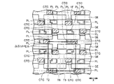
次に、本実施の形態の半導体装置の具体的な構成について、図4〜図8を用いて説明する。なお図4〜図6において太線で囲まれた領域は1つのSRAMメモリセル(ユニットセル)の形成領域を示している。 Next, a specific configuration of the semiconductor device of this embodiment will be described with reference to FIGS. 4 to 6, a region surrounded by a thick line indicates a region where one SRAM memory cell (unit cell) is formed.
図4を参照して、半導体基板SUBの主表面にはSTIなどの素子分離構造が形成されており、その素子分離構造によって複数の活性領域1Fが半導体基板SUBの主表面において互いに電気的に分離されている。この活性領域1Fは、図4中上下方向に延在している。この活性領域1Fと直交するようにゲート電極GEが、図4中左右方向に延在している。この活性領域1Fとゲート電極GEとの交差部付近に、SRAMメモリセルに含まれる各トランジスタT1、T2、T5、T6が形成されている。
Referring to FIG. 4, an element isolation structure such as STI is formed on the main surface of semiconductor substrate SUB, and a plurality of
図7を参照して、トランジスタT1、T2、T5、T6の各々は、半導体基板SUBの主表面において活性領域1Fに形成された1対のソース/ドレイン領域SDと、その1対のソース/ドレイン領域SDに挟まれる半導体基板SUBの主表面上にゲート絶縁膜GIを介在して形成されたゲート電極GEとを有している。
Referring to FIG. 7, each of transistors T1, T2, T5, T6 includes a pair of source / drain regions SD formed in
図4を参照して、ユニットセル内において、ドライバトランジスタT1のドレイン領域とアクセストランジスタT5のソース領域とは共通の不純物領域から構成されており、互いに電気的に接続されている。またドライバトランジスタT2のドレイン領域とアクセストランジスタT6のソース領域とは共通の不純物領域から構成されており、互いに電気的に接続されている。またアクセストランジスタT5のゲート電極GEとアクセストランジスタT6のゲート電極GEとは共通の導電層により一体となるよう構成されており、互いに電気的に接続されている。 Referring to FIG. 4, in the unit cell, the drain region of driver transistor T1 and the source region of access transistor T5 are formed of a common impurity region and are electrically connected to each other. The drain region of driver transistor T2 and the source region of access transistor T6 are formed of a common impurity region and are electrically connected to each other. Further, the gate electrode GE of the access transistor T5 and the gate electrode GE of the access transistor T6 are configured to be integrated by a common conductive layer and are electrically connected to each other.
また図4中上下方向に隣り合うユニットセル間においては、ドライバトランジスタT1のソース領域同士が共通の不純物領域から構成されており、互いに電気的に接続されている。また図4中上下方向に隣り合うユニットセル間においては、ドライバトランジスタT2のソース領域同士も共通の不純物領域から構成されており、互いに電気的に接続されている。また図4中左右方向に隣り合うユニットセル間においては、アクセストランジスタT5、T6のゲート電極GE同士が各ユニットセル間で一体となるように構成されており、互いに電気的に接続されている。 In addition, between the unit cells adjacent in the vertical direction in FIG. 4, the source regions of the driver transistor T1 are composed of a common impurity region and are electrically connected to each other. Further, between the unit cells adjacent in the vertical direction in FIG. 4, the source regions of the driver transistor T2 are also composed of a common impurity region and are electrically connected to each other. Also, between unit cells adjacent in the left-right direction in FIG. 4, the gate electrodes GE of the access transistors T5 and T6 are configured to be integrated between the unit cells and are electrically connected to each other.
図7を参照して、トランジスタT1、T2、T5、T6の各々のゲート電極GEは、たとえばドープトポリシリコン膜GE1と、タングステンシリサイド膜GE2とが積層されたいわゆるポリサイド構造となっている。またトランジスタT1、T2、T5、T6の各々のゲート電極GEは、ドープトポリシリコン膜単層からなっていてもよい。 Referring to FIG. 7, each gate electrode GE of transistors T1, T2, T5, T6 has a so-called polycide structure in which, for example, a doped polysilicon film GE1 and a tungsten silicide film GE2 are stacked. The gate electrodes GE of the transistors T1, T2, T5, and T6 may be formed of a single layer of doped polysilicon film.
ゲート電極GE上には絶縁膜HMが形成されている。この絶縁膜HMは、たとえばTEOS(Tetra Ethyl Ortho Silicate)を原料として形成されたシリコン酸化膜とシリコン窒化膜との積層構造よりなっている。 An insulating film HM is formed on the gate electrode GE. The insulating film HM has a laminated structure of a silicon oxide film and a silicon nitride film formed using, for example, TEOS (Tetra Ethyl Ortho Silicate) as a raw material.
ゲート絶縁膜GIおよびゲート電極GEの側壁には、たとえばシリコン酸化膜よりなる絶縁膜NOが形成されている。またゲート絶縁膜GI、ゲート電極GEおよび絶縁膜HMの積層構造の側壁には、絶縁膜NOの側部を覆うように側壁絶縁膜SWが形成されている。側壁絶縁膜SWは、シリコン窒化膜で形成されても、シリコン酸化膜とシリコン窒化膜との組合せで形成されてもよい。 An insulating film NO made of, for example, a silicon oxide film is formed on the side walls of the gate insulating film GI and the gate electrode GE. A sidewall insulating film SW is formed on the side wall of the stacked structure of the gate insulating film GI, the gate electrode GE, and the insulating film HM so as to cover the side portion of the insulating film NO. Sidewall insulating film SW may be formed of a silicon nitride film or a combination of a silicon oxide film and a silicon nitride film.
図7および図8を参照して、半導体基板SUBの主表面上には、ライナー膜ILと、層間絶縁膜II1と、絶縁膜IIとが下から順に形成されている。SRAMメモリセルの形成領域内においては、ソース/ドレイン領域SD上のライナー膜IL、層間絶縁膜II1および絶縁膜IIが選択的に除去されている。これにより、ライナー膜IL、層間絶縁膜II1および絶縁膜IIの各々を貫通してソース/ドレイン領域SDに達するコンタクトホールCH1が形成されている。このコンタクトホールCH1の内部には、ソース/ドレイン領域SDに接続されたプラグ導電層PLが形成されている。このプラグ導電層PLの上面の高さ位置は、層間絶縁膜II1の上面の高さ位置よりも低く、かつ絶縁膜HMの上面の高さ位置と同じかそれよりも低い。 Referring to FIGS. 7 and 8, a liner film IL, an interlayer insulating film II1, and an insulating film II are formed in this order from the bottom on the main surface of the semiconductor substrate SUB. In the SRAM memory cell formation region, the liner film IL, the interlayer insulating film II1, and the insulating film II on the source / drain region SD are selectively removed. As a result, a contact hole CH1 penetrating each of the liner film IL, the interlayer insulating film II1 and the insulating film II and reaching the source / drain region SD is formed. Inside the contact hole CH1, a plug conductive layer PL connected to the source / drain region SD is formed. The height position of the upper surface of the plug conductive layer PL is lower than the height position of the upper surface of the interlayer insulating film II1, and is the same as or lower than the height position of the upper surface of the insulating film HM.
図4を参照して、コンタクトホールCH1は、1つの活性領域1Fにおけるドライバトランジスタの1対のソース/ドレイン領域SDと、アクセストランジスタの1対のソース/ドレイン領域SDとの上方を繋ぐように開口している。このためコンタクトホールCH1は、図4中上下方向に隣り合うユニットセル間を跨ぐように開口している。本実施の形態においては、1つのコンタクトホールCH1の開口内に5つの互いに分離したプラグ導電層PLが配置されている。このプラグ導電層PLは、たとえばドープトポリシリコン膜からなっている。
Referring to FIG. 4, contact hole CH1 is opened to connect a pair of source / drain regions SD of the driver transistor and a pair of source / drain regions SD of the access transistor in one
図7および図8を参照して、プラグ導電層PL、絶縁膜HM、IIなどの上に層間絶縁膜II2が形成されている。この層間絶縁膜II2には、複数のスルーホールTHが形成されている。複数のスルーホールTHは、アクセストランジスタT5、T6の各ドレイン領域に接続されたプラグ導電層PLに達するスルーホールTHと、ドライバトランジスタT1、T2の各ソース領域に接続されたプラグ導電層PLに達するスルーホールTHとを含んでいる。 7 and 8, interlayer insulating film II2 is formed on plug conductive layer PL, insulating films HM, II, and the like. A plurality of through holes TH are formed in the interlayer insulating film II2. The plurality of through holes TH reach the plug conductive layer PL connected to the drain regions of the access transistors T5 and T6 and the plug conductive layer PL connected to the source regions of the driver transistors T1 and T2. Through hole TH is included.
これらのスルーホールTHの各々からはプラグ導電層PLの上面の一部と側面の一部とが露出している。またスルーホールTH(コンタクト導電層用穴)の各々は、層間絶縁膜II1内において、コンタクトホールCH1(プラグ導電層用穴)と互いに接続されるように形成されている。 From each of these through holes TH, a part of the upper surface and a part of the side surface of the plug conductive layer PL are exposed. Each of the through holes TH (contact conductive layer holes) is formed in the interlayer insulating film II1 so as to be connected to the contact hole CH1 (plug conductive layer hole).
このスルーホールTH内にはコンタクト導電層CTCが形成されている。このコンタクト導電層CTCは、スルーホールTHから露出したプラグ導電層PLの上面の一部と側面の一部との双方に接するように形成されている。このコンタクト導電層CTCは、たとえばTi(チタン)/TiN(窒化チタン)層とW(タングステン)層とから構成されている。 A contact conductive layer CTC is formed in the through hole TH. The contact conductive layer CTC is formed so as to be in contact with both part of the upper surface and part of the side surface of the plug conductive layer PL exposed from the through hole TH. This contact conductive layer CTC is composed of, for example, a Ti (titanium) / TiN (titanium nitride) layer and a W (tungsten) layer.
図5を参照して、コンタクト導電層CTCは、平面視において(半導体基板SUBの主表面に対して直交する方向からみて)コンタクト導電層CTCが接続されるプラグ導電層PLに対して、各トランジスタT1、T2、T5、T6のチャネル幅方向(図5中左右方向)に突き出すように(ずれるように)形成されている。これによりコンタクト導電層CTCは、プラグ導電層PLのチャネル幅方向に互いに対向する両側面の少なくとも一方の側面に接続されている。 Referring to FIG. 5, contact conductive layer CTC is connected to each plug conductive layer PL to which contact conductive layer CTC is connected in plan view (as viewed from the direction orthogonal to the main surface of semiconductor substrate SUB). It is formed so as to protrude (displace) in the channel width direction (left and right direction in FIG. 5) of T1, T2, T5, and T6. Thus, the contact conductive layer CTC is connected to at least one side surface of the plug conductive layer PL facing each other in the channel width direction.
図8を参照して、コンタクト導電層CTCに電気的に接続するように層間絶縁膜II2上にビット線BLなどの配線層が形成されている。このビット線BLなどの配線層は、その配線層が接続されるコンタクト導電層CTCと同一の層により一体に形成されている。このためビット線BLなどの配線層は、コンタクト導電層CTCと同じ材質である、Ti(チタン)/TiN(窒化チタン)層とW(タングステン)層とから構成されている。 Referring to FIG. 8, a wiring layer such as bit line BL is formed on interlayer insulating film II2 so as to be electrically connected to contact conductive layer CTC. The wiring layer such as the bit line BL is integrally formed of the same layer as the contact conductive layer CTC to which the wiring layer is connected. Therefore, the wiring layer such as the bit line BL is composed of a Ti (titanium) / TiN (titanium nitride) layer and a W (tungsten) layer, which are the same material as the contact conductive layer CTC.
図6を参照して、ビット線BLは、コンタクト導電層CTCとプラグ導電層PLとを介してアクセストランジスタT5のドレイン領域に電気的に接続されている。ビット線/BLは、コンタクト導電層CTCとプラグ導電層PLとを介してアクセストランジスタT6のドレイン領域に電気的に接続されている。グランド配線GNDは、コンタクト導電層CTCとプラグ導電層PLとを介してドライバトランジスタT1のソース領域に電気的に接続されている。またグランド配線GNDは、コンタクト導電層CTCとプラグ導電層PLとを介してドライバトランジスタT2のソース領域に電気的に接続されている。 Referring to FIG. 6, bit line BL is electrically connected to the drain region of access transistor T5 through contact conductive layer CTC and plug conductive layer PL. Bit line / BL is electrically connected to the drain region of access transistor T6 through contact conductive layer CTC and plug conductive layer PL. The ground wiring GND is electrically connected to the source region of the driver transistor T1 through the contact conductive layer CTC and the plug conductive layer PL. The ground wiring GND is electrically connected to the source region of the driver transistor T2 through the contact conductive layer CTC and the plug conductive layer PL.
ビット線BL、/BLおよびグランド配線GNDの各配線層は、上述のとおりコンタクト導電層CTCと同じ材質から構成されている。また各配線層BL、/BL、GNDは、プラグ導電層PLの真上に位置しない領域においてコンタクト導電層CTCと接続された部分を有している。各配線層BL、/BL、GNDは、その長さ方向の全体がプラグ導電層PLの真上に位置しない領域に配置されていることが好ましい。また各配線層BL、/BL、GNDは、平面視においてメモリセルの形成領域を直線状に延びて横断していることが好ましい。 Each wiring layer of the bit lines BL, / BL and the ground wiring GND is made of the same material as the contact conductive layer CTC as described above. Each of the wiring layers BL, / BL, GND has a portion connected to the contact conductive layer CTC in a region not directly above the plug conductive layer PL. Each wiring layer BL, / BL, GND is preferably arranged in a region where the entire length direction is not located immediately above the plug conductive layer PL. Each of the wiring layers BL, / BL, GND preferably extends linearly across the memory cell formation region in plan view.
各配線層BL、/BL、GNDよりも上層の構成については、図3を用いて説明した構成とほぼ同じであるため、その説明は繰り返さない。 Since the configuration above each wiring layer BL, / BL, GND is substantially the same as the configuration described with reference to FIG. 3, the description thereof will not be repeated.
次に、本実施の形態の半導体装置の製造方法について説明する。
図9(A)、(B)、(C)を参照して、シリコン基板SUB上に素子分離構造を構成する絶縁膜SIがたとえばシリコン酸化膜から形成される。その後、イオン注入や熱処理が行われて、p型ウエル領域PWLとn型ウエル領域NWLとが形成される。
Next, a method for manufacturing the semiconductor device of the present embodiment will be described.
Referring to FIGS. 9A, 9B, and 9C, an insulating film SI constituting an element isolation structure is formed on a silicon substrate SUB, for example, from a silicon oxide film. Thereafter, ion implantation and heat treatment are performed to form a p-type well region PWL and an n-type well region NWL.
図10(A)、(B)、(C)を参照して、ゲート絶縁膜GIとゲート電極GEとが形成される。ゲート電極GEは、たとえばドープトポリシリコン膜GE1と、タングステンシリサイド膜GE2とが積層されたいわゆるポリサイド構造で形成される。ゲート電極GE上には、後工程のSAC(Self Align Contact)時にエッチングストッパ膜として機能する絶縁膜HMが形成される。絶縁膜HMは、たとえばSiN膜の単層や、SiN膜とTEOS膜(SiO2膜)との多層などから形成される。
Referring to FIGS. 10A, 10B, and 10C, gate insulating film GI and gate electrode GE are formed. The gate electrode GE is formed of, for example, a so-called polycide structure in which a doped polysilicon film GE1 and a tungsten silicide film GE2 are stacked. On the gate electrode GE, an insulating film HM that functions as an etching stopper film at the time of SAC (Self Align Contact) in a subsequent process is formed. The insulating film HM is formed from, for example, a single layer of a SiN film or a multilayer of a SiN film and a TEOS film (
その後、ゲート電極GEの側壁にはトランジスタの電界緩和用の酸化などによりシリコン酸化膜よりなる絶縁膜NOが形成される。その後、ソース/ドレイン形成用のイオン注入などが行われた後に、ゲート絶縁膜GI、ゲート電極GEおよび絶縁膜HMの側壁を覆う側壁絶縁膜SWがたとえばSiN膜などの絶縁膜から形成される。その後、さらにソース/ドレイン形成用のイオン注入が行われて、LDD(Lightly Doped Drain)構造のソース/ドレイン領域SDが形成される。 Thereafter, an insulating film NO made of a silicon oxide film is formed on the sidewall of the gate electrode GE by oxidation for electric field relaxation of the transistor or the like. Thereafter, after ion implantation for source / drain formation is performed, a sidewall insulating film SW covering the sidewalls of the gate insulating film GI, the gate electrode GE, and the insulating film HM is formed from an insulating film such as a SiN film. Thereafter, ion implantation for forming a source / drain is further performed to form a source / drain region SD having an LDD (Lightly Doped Drain) structure.
図11(A)、(B)、(C)を参照して、表面全面に、たとえばSiN膜よりなるライナー膜ILが形成される。 Referring to FIGS. 11A, 11B, and 11C, a liner film IL made of, for example, a SiN film is formed on the entire surface.
図12(A)、(B)、(C)を参照して、ライナー膜IL上に、たとえばBP(Boro Phospho)TEOSなどからなる層間絶縁膜II1が形成される。この層間絶縁膜II1は熱処理を加えられてある程度平坦化される。この後、層間絶縁膜II1にCMP(Chemical Mechanical Polishing)処理が施されることにより、層間絶縁膜II1はライナー膜ILが露出するまで研磨除去されて、その上面が平坦化される。 12A, 12B, and 12C, an interlayer insulating film II1 made of, for example, BP (Boro Phospho) TEOS or the like is formed on liner film IL. This interlayer insulating film II1 is flattened to some extent by heat treatment. Thereafter, CMP (Chemical Mechanical Polishing) processing is performed on the interlayer insulating film II1, whereby the interlayer insulating film II1 is polished and removed until the liner film IL is exposed, and the upper surface thereof is flattened.
図13(A)、(B)、(C)を参照して、平坦化された層間絶縁膜II1上に、たとえばTEOSを原料としたシリコン酸化膜よりなる絶縁膜IIが形成される。この絶縁膜II上に、通常の写真製版技術によりレジストパターンPR1が形成される。このレジストパターンPR1をマスクとして絶縁膜IIと層間絶縁膜II1とがエッチングにより選択的に除去される。この後、レジストパターンPR1がたとえばアッシングなどにより除去される。 Referring to FIGS. 13A, 13B, and 13C, an insulating film II made of, for example, a silicon oxide film using TEOS as a raw material is formed on the planarized interlayer insulating film II1. A resist pattern PR1 is formed on the insulating film II by a normal photolithography technique. Using this resist pattern PR1 as a mask, insulating film II and interlayer insulating film II1 are selectively removed by etching. Thereafter, resist pattern PR1 is removed by, for example, ashing.
図14(A)、(B)、(C)を参照して、上記の絶縁膜IIと層間絶縁膜II1とのエッチング除去により、絶縁膜IIと層間絶縁膜II1とに開口部が形成され、層間絶縁膜II1の下層のライナー膜ILが露出する。露出したライナー膜ILがエッチングにより除去される。 Referring to FIGS. 14A, 14B, and 14C, an opening is formed in insulating film II and interlayer insulating film II1 by etching removal of insulating film II and interlayer insulating film II1. The liner film IL under the interlayer insulating film II1 is exposed. The exposed liner film IL is removed by etching.
図15(A)、(B)、(C)を参照して、上記のライナー膜ILのエッチング除去により、ソース/ドレイン領域SDを露出させるコンタクトホールCH1が絶縁膜IL、II1、IIに形成される。 Referring to FIGS. 15A, 15B, and 15C, contact hole CH1 exposing source / drain region SD is formed in insulating films IL, II1, and II by etching removal of liner film IL described above. The
図16(A)、(B)、(C)を参照して、コンタクトホールCH1内を埋め込むように、たとえばリンがドープされたドープトポリシリコンよりなる導電層PLが絶縁膜II上に形成される。この導電層PLに全面エッチバックが施される。 Referring to FIGS. 16A, 16B, and 16C, a conductive layer PL made of, for example, doped polysilicon doped with phosphorus is formed on the insulating film II so as to fill the contact hole CH1. The The entire surface of the conductive layer PL is etched back.
図17(A)、(B)、(C)を参照して、上記の全面エッチバックにより、導電層PLの上面の高さ位置が絶縁膜II、II1の上面の高さ位置よりも低く、かつ絶縁膜HMの上面の高さ位置と同じかそれよりも低くなる。これにより導電層PLから互いに分離した複数のプラグ導電層PLが形成される。1つのコンタクトホールCH1内の複数のプラグ導電層PLはゲート電極GEにより分離される。 Referring to FIGS. 17A, 17B, and 17C, the height position of the upper surface of the conductive layer PL is lower than the height position of the upper surfaces of the insulating films II and II1 by the above-described overall etch-back. In addition, the height is the same as or lower than the height of the upper surface of the insulating film HM. Thereby, a plurality of plug conductive layers PL separated from the conductive layer PL are formed. The plurality of plug conductive layers PL in one contact hole CH1 are separated by the gate electrode GE.
図18(A)、(B)、(C)を参照して、表面全面に層間絶縁膜II2が形成される。この層間絶縁膜II2は、層間絶縁膜II1と同一の材質でもよく、また異なる材質でもよい。 Referring to FIGS. 18A, 18B, and 18C, an interlayer insulating film II2 is formed on the entire surface. The interlayer insulating film II2 may be the same material as the interlayer insulating film II1 or may be a different material.
図19(A)、(B)、(C)を参照して、通常の写真製版技術およびエッチング技術により周辺回路の形成領域にコンタクトホールCH2が形成される。このコンタクトホールCH2は、ゲート電極GEに達するものと、半導体基板SUBの主表面の不純物領域に達するものとを含む。 Referring to FIGS. 19A, 19B, and 19C, contact hole CH2 is formed in the peripheral circuit formation region by a normal photoengraving technique and etching technique. This contact hole CH2 includes one that reaches the gate electrode GE and one that reaches the impurity region on the main surface of the semiconductor substrate SUB.
図20(A)、(B)、(C)を参照して、通常の写真製版技術およびエッチング技術により、メモリセルの形成領域にスルーホールTHが形成される。このスルーホールTHはプラグ導電層PLの上面の一部と側面の一部との双方を露出するように形成される。つまりスルーホールTHは、層間絶縁膜II1の内部にまで達するように形成されて、層間絶縁膜II1の内部においてコンタクトホールCH1と互いに接続されるように形成される。 Referring to FIGS. 20A, 20B, and 20C, through holes TH are formed in the memory cell formation region by a normal photolithography technique and etching technique. The through hole TH is formed so as to expose both a part of the upper surface and a part of the side surface of the plug conductive layer PL. That is, the through hole TH is formed so as to reach the inside of the interlayer insulating film II1, and is formed so as to be connected to the contact hole CH1 inside the interlayer insulating film II1.
図21(A)、(B)、(C)を参照して、スルーホールTHおよびコンタクトホールCH2のそれぞれの内部を埋め込むように層間絶縁膜II2の上に導電層CFが形成される。この導電層CFは、たとえばTi/TiNのバリアメタル層とWの配線層とから形成される。 Referring to FIGS. 21A, 21B, and 21C, conductive layer CF is formed on interlayer insulating film II2 so as to embed each inside of through hole TH and contact hole CH2. The conductive layer CF is formed of, for example, a Ti / TiN barrier metal layer and a W wiring layer.
図22(A)、(B)、(C)を参照して、導電層CFが、通常の写真製版技術およびエッチング技術によりパターニングされる。これにより導電層CFから、メモリセルの形成領域ではコンタクト導電層CTCと配線層BL、/BL、GNDとが一体で形成され、周辺回路の形成領域では配線層ICLが形成される。このようにして本実施の形態の半導体装置が製造される。 Referring to FIGS. 22A, 22B, and 22C, conductive layer CF is patterned by a normal photolithography technique and etching technique. As a result, the contact conductive layer CTC and the wiring layers BL, / BL, GND are integrally formed from the conductive layer CF in the memory cell formation region, and the wiring layer ICL is formed in the peripheral circuit formation region. In this way, the semiconductor device of the present embodiment is manufactured.
次に、図23〜図34に示す関連技術を説明したうえで、その関連技術と対比して本実施の形態の作用効果について説明する。 Next, after describing the related technique shown in FIGS. 23 to 34, the operational effects of the present embodiment will be described in comparison with the related technique.
図23〜図26を参照して、関連技術の構成は、コンタクト導電層CTCがプラグ導電層PLの上面にのみ接して形成されている点で、本実施の形態の構成と異なっている。このため関連技術の構成では、図23に示すようにプラグ導電層PLの上面の寸法が大きく、かつ平面視においてコンタクト導電層CTCはプラグ導電層PLの配置位置から突き出していない。また図24に示すように各配線層BL、/BL、GNDは、ユニットセル内において平面視で一直線状に配置することはできず、折れ曲がっている。 23 to 26, the configuration of the related art is different from the configuration of the present embodiment in that contact conductive layer CTC is formed in contact with only the upper surface of plug conductive layer PL. Therefore, in the configuration of the related art, as shown in FIG. 23, the size of the upper surface of the plug conductive layer PL is large, and the contact conductive layer CTC does not protrude from the arrangement position of the plug conductive layer PL in plan view. In addition, as shown in FIG. 24, the wiring layers BL, / BL, GND cannot be arranged in a straight line in the unit cell, and are bent.
また図25に示すように、プラグ導電層PLの上面の高さ位置は層間絶縁膜II1の上面の高さ位置と同じであり、かつゲート電極GE上の絶縁膜HMの上面の高さ位置よりも高い。また図26に示すように、配線層BL、/BL、GNDの各々は、それらが電気的に接続されるプラグ導電層PLの真上の領域上に位置している。 Further, as shown in FIG. 25, the height position of the upper surface of the plug conductive layer PL is the same as the height position of the upper surface of the interlayer insulating film II1, and from the height position of the upper surface of the insulating film HM on the gate electrode GE. Is also expensive. As shown in FIG. 26, each of the wiring layers BL, / BL, GND is located on a region immediately above the plug conductive layer PL to which they are electrically connected.
なお、上記以外の関連技術の構成は本実施の形態の構成とほぼ同じであるため、同一の要素については同一の符号を付し、その説明を繰り返さない。 In addition, since the structure of related technology other than the above is substantially the same as the structure of this Embodiment, the same code | symbol is attached | subjected about the same element and the description is not repeated.
この関連技術の製造方法は、たとえば以下のとおりである。
関連技術の製造方法は、まず図9〜図11に示す本実施の形態の製造方法と同一の工程を経る。この後、図27を参照して、トランジスタTGを覆うように層間絶縁膜II1が形成される。
The manufacturing method of this related technique is as follows, for example.
The related art manufacturing method first undergoes the same steps as the manufacturing method of the present embodiment shown in FIGS. Thereafter, referring to FIG. 27, interlayer insulating film II1 is formed to cover transistor TG.
図28を参照して、層間絶縁膜II1にコンタクトホールCH1が形成される。このコンタクトホールCH1は、ソース/ドレイン領域SD毎に1つずつ形成される。 Referring to FIG. 28, contact hole CH1 is formed in interlayer insulating film II1. One contact hole CH1 is formed for each source / drain region SD.
図29を参照して、各コンタクトホールCH1を埋め込むように層間絶縁膜II1上に導電層PLが形成される。この導電層PLに全面エッチバック処理かあるいはCMP処理が施される。 Referring to FIG. 29, conductive layer PL is formed on interlayer insulating film II1 so as to fill each contact hole CH1. This conductive layer PL is subjected to an overall etch back process or a CMP process.
図30を参照して、上記の全面エッチバック処理あるいはCMP処理により導電層PLが研磨除去されて、層間絶縁膜II1の上面が露出する。これにより、各コンタクトホールCH1を埋め込むプラグ導電層PLが導電層PLから形成される。 Referring to FIG. 30, conductive layer PL is polished and removed by the above-described overall etch-back process or CMP process, and the upper surface of interlayer insulating film II1 is exposed. As a result, a plug conductive layer PL filling each contact hole CH1 is formed from the conductive layer PL.
図31を参照して、層間絶縁膜II1およびプラグ導電層PL上に層間絶縁膜II2が形成される。 Referring to FIG. 31, interlayer insulating film II2 is formed on interlayer insulating film II1 and plug conductive layer PL.
図32を参照して、層間絶縁膜II2にスルーホールTHとコンタクトホールCH2とが形成される。スルーホールTHはプラグ導電層PLの上面のみを露出するように形成される。またコンタクトホールCH2はゲート電極GEまたは半導体基板SUBの主表面の不純物領域に達するように形成される。 Referring to FIG. 32, through hole TH and contact hole CH2 are formed in interlayer insulating film II2. Through hole TH is formed to expose only the upper surface of plug conductive layer PL. Contact hole CH2 is formed to reach the impurity region on the main surface of gate electrode GE or semiconductor substrate SUB.
図33を参照して、スルーホールTHおよびコンタクトホールCH2内を埋め込むように層間絶縁膜II2上に導電層CFが形成される。 Referring to FIG. 33, conductive layer CF is formed on interlayer insulating film II2 so as to fill in through hole TH and contact hole CH2.
図34を参照して、導電層CFがパターニングされて導電層CFからコンタクト導電層CTCと、配線層BL、/BL、GNDと、配線層ICLとが形成される。このように関連技術は製造される。 Referring to FIG. 34, conductive layer CF is patterned to form contact conductive layer CTC, wiring layers BL, / BL, GND, and wiring layer ICL from conductive layer CF. In this way, the related technology is manufactured.
関連技術の構成では、図26に示すようにコンタクト導電層CTCをプラグ導電層PLの上面のみに接続するよう形成するため、プラグ導電層PLの上面の寸法を十分に大きくする必要がある。しかし、デバイスの微細化に伴い、そのような大きな寸法の上面を有するプラグ導電層PLのパターンの形成が困難となっている。 In the configuration of the related art, as shown in FIG. 26, the contact conductive layer CTC is formed so as to be connected only to the upper surface of the plug conductive layer PL. Therefore, it is necessary to sufficiently increase the size of the upper surface of the plug conductive layer PL. However, with the miniaturization of devices, it is difficult to form a pattern of the plug conductive layer PL having an upper surface with such a large dimension.
また1つのメモリセルの形成領域内に配線される3本の配線層BL、/BL、GNDはスルーホールTHと接続するために折れ曲がって配置する必要があった。しかしコンタクト導電層CTCがプラグ導電層PLの上面のみに接続されるという制約下では、デバイスの微細化にともなってコンタクト導電層CTCの配置が困難となってきている。 Further, the three wiring layers BL, / BL, GND wired in the formation region of one memory cell have to be bent and arranged in order to connect with the through hole TH. However, under the restriction that the contact conductive layer CTC is connected only to the upper surface of the plug conductive layer PL, it is difficult to dispose the contact conductive layer CTC as the device is miniaturized.
また図26に示すようにコンタクト導電層CTCとビット線BLなどの配線層とが同一の層から一体として形成されることにより、ビット線BLなどの配線層の倒れに対するマージンが向上されている。しかしながらデバイスの微細化によりコンタクト導電層CTCのサイズが小さくなり、また縦方向にもスケーリングが進むことにより、スルーホールTHの深さが浅くなり、ビット線BLなどの配線層の倒れに対するマージンもなくなってきている。 In addition, as shown in FIG. 26, the contact conductive layer CTC and the wiring layer such as the bit line BL are integrally formed from the same layer, thereby improving the margin against the collapse of the wiring layer such as the bit line BL. However, as the device is miniaturized, the size of the contact conductive layer CTC is reduced, and the vertical scaling increases the depth of the through hole TH, thereby eliminating the margin for the collapse of the wiring layer such as the bit line BL. It is coming.
これに対して本実施の形態においては、図8に示すようにプラグ導電層PLの上面および側面の双方に接するようにコンタクト導電層CTCが形成されている。このためプラグ導電層PLとコンタクト導電層CTCとの確実な接続が容易となる。よってデバイスの微細化にともなってプラグ導電層PLの上面の寸法を小さくしてもプラグ導電層PLとコンタクト導電層CTCとを確実に接続することができる。 In contrast, in the present embodiment, as shown in FIG. 8, contact conductive layer CTC is formed so as to be in contact with both the upper surface and the side surface of plug conductive layer PL. This facilitates reliable connection between the plug conductive layer PL and the contact conductive layer CTC. Therefore, the plug conductive layer PL and the contact conductive layer CTC can be reliably connected even if the size of the upper surface of the plug conductive layer PL is reduced with the miniaturization of the device.
また本実施の形態においては、図8に示すようにプラグ導電層PLの上面および側面の双方に接するようにコンタクト導電層CTCが形成されている。このため、そのコンタクト導電層CTCと一体に形成される配線層BL、/BL、GNDの配置の自由度が向上する。よってデバイスが微細化されても、3本の配線層BL、/BL、GNDの等ピッチでの配置に容易に対応することができる。 In the present embodiment, as shown in FIG. 8, contact conductive layer CTC is formed so as to be in contact with both the upper surface and the side surface of plug conductive layer PL. For this reason, the degree of freedom of arrangement of the wiring layers BL, / BL, GND formed integrally with the contact conductive layer CTC is improved. Therefore, even if the device is miniaturized, it is possible to easily cope with the arrangement of the three wiring layers BL, / BL, GND at an equal pitch.
また本実施の形態においては、図8に示すようにプラグ導電層PLの上面および側面の双方に接するようにコンタクト導電層CTCが形成されている。このため、コンタクト導電層CTCを関連技術のコンタクト導電層CTCよりも下側の深い位置にまで延ばすことが可能となる。これにより、配線層BL、/BL、GNDの倒れに対するマージンを大きく確保することができ直線で配置することも可能である。なお、パターンを直線状に配置することで折り曲げて配置する場合に比べて、写真製版時のマージンを拡大することができる。 In the present embodiment, as shown in FIG. 8, contact conductive layer CTC is formed so as to be in contact with both the upper surface and the side surface of plug conductive layer PL. Therefore, the contact conductive layer CTC can be extended to a deeper position below the contact conductive layer CTC of the related art. As a result, a large margin against the collapse of the wiring layers BL, / BL, GND can be secured, and the wiring layers BL, / BL, GND can be arranged linearly. In addition, the margin at the time of photoengraving can be expanded compared to the case where the pattern is arranged in a straight line, compared with the case where the pattern is bent.
また本実施の形態においては、図8に示すように配線層BL、/BL、GNDは、プラグ導電層PLの真上に位置しない領域においてコンタクト導電層CTCと接続されている。これにより、配線層BL、/BL、GNDの平面視における配置の自由度が向上する。 In the present embodiment, as shown in FIG. 8, the wiring layers BL, / BL, GND are connected to the contact conductive layer CTC in a region not directly above the plug conductive layer PL. As a result, the degree of freedom in arrangement of the wiring layers BL, / BL, GND in a plan view is improved.
また本実施の形態においては、図8に示すように層間絶縁膜II1内においてコンタクトホールCH1とスルーホールTHとが互いに接続されるように形成されている。これにより、コンタクト導電層CTCを関連技術のコンタクト導電層CTCよりも下側の深い位置にまで延ばすことが可能となり、配線層BL、/BL、GNDの倒れに対するマージンを大きく確保することができる。 Further, in the present embodiment, as shown in FIG. 8, the contact hole CH1 and the through hole TH are formed in the interlayer insulating film II1 so as to be connected to each other. As a result, the contact conductive layer CTC can be extended to a deeper position below the contact conductive layer CTC of the related art, and a large margin for the collapse of the wiring layers BL, / BL, GND can be secured.
また本実施の形態においては、プラグ導電層PLの上面の高さ位置は層間絶縁膜の上面の高さ位置よりも低い。これにより、プラグ導電層PL上に形成されるコンタクト導電層CTCの厚みを厚くすることができる。よって、配線層の倒れを抑制することができる。 In the present embodiment, the height position of the upper surface of plug conductive layer PL is lower than the height position of the upper surface of the interlayer insulating film. Thereby, the thickness of the contact conductive layer CTC formed on the plug conductive layer PL can be increased. Therefore, the wiring layer can be prevented from falling.
また本実施の形態においては、図5に示すように平面視においてコンタクト導電層CTCはプラグ導電層PLに対してトランジスタTGのチャネル幅方向に突き出すように配置されている。このため、そのコンタクト導電層CTCに接続される配線層BL、/BL、GNDのチャネル幅方向の配置の自由度が向上する。 In the present embodiment, as shown in FIG. 5, the contact conductive layer CTC is arranged so as to protrude in the channel width direction of the transistor TG with respect to the plug conductive layer PL in plan view. For this reason, the freedom degree of arrangement of the wiring layers BL, / BL, GND connected to the contact conductive layer CTC in the channel width direction is improved.
また本実施の形態においては、図4あるいは図7に示すようにゲート電極GEと対向するプラグ導電層PLの面積を減らすことができ、ゲート電極GEとプラグ導電層PLとの間によるビット線容量を低減することができる。 In the present embodiment, as shown in FIG. 4 or FIG. 7, the area of the plug conductive layer PL facing the gate electrode GE can be reduced, and the bit line capacitance between the gate electrode GE and the plug conductive layer PL can be reduced. Can be reduced.
(実施の形態2)
実施の形態1においては、図8に示すようにコンタクト導電層CTCの底面がライナー膜ILに達しない(つまりコンタクト導電層CTCの底面が層間絶縁膜II2よりなる)場合について説明した。しかし図35に示す本実施の形態のように、コンタクト導電層CTCの底面はライナー膜ILに達していてもよい。つまりコンタクト導電層CTCの底面がライナー膜ILよりなっていてもよい。
(Embodiment 2)
In the first embodiment, the case where the bottom surface of the contact conductive layer CTC does not reach the liner film IL (that is, the bottom surface of the contact conductive layer CTC is formed of the interlayer insulating film II2) has been described as shown in FIG. However, as in the present embodiment shown in FIG. 35, the bottom surface of the contact conductive layer CTC may reach the liner film IL. That is, the bottom surface of the contact conductive layer CTC may be made of the liner film IL.
なおこれ以外の本実施の形態の構成は、図8に示す実施の形態1の構成をほぼ同じであるため同一の要素については同一の符号を付しその説明を繰り返さない。
In addition, since the structure of this Embodiment other than this is as substantially the structure of
本実施の形態の製造方法は、まず図9〜図19に示す実施の形態1の工程と同様の工程を経る。この後、図36(A)、(B)を参照して、通常の写真製版技術およびエッチング技術により、メモリセルの形成領域にスルーホールTHが形成される。このスルーホールTHは、ライナー膜ILに達するように形成されて、かつ層間絶縁膜II1の内部においてコンタクトホールCH1と互いに接続されるように形成される。これにより、スルーホールTHはプラグ導電層PLの上面の一部と側面の一部との双方を露出するように形成される。 The manufacturing method of the present embodiment first undergoes the same steps as those of the first embodiment shown in FIGS. Thereafter, referring to FIGS. 36A and 36B, through holes TH are formed in the memory cell formation region by a normal photolithography technique and etching technique. The through hole TH is formed so as to reach the liner film IL, and is formed so as to be connected to the contact hole CH1 inside the interlayer insulating film II1. Thus, the through hole TH is formed so as to expose both a part of the upper surface and a part of the side surface of the plug conductive layer PL.
図37(A)、(B)を参照して、スルーホールTHおよびコンタクトホールCH2のそれぞれの内部を埋め込むように層間絶縁膜II2の上に導電層CFが形成される。この導電層CFは、たとえばTi/TiNのバリアメタル層とWの配線層とから形成される。 Referring to FIGS. 37A and 37B, conductive layer CF is formed on interlayer insulating film II2 so as to embed each inside of through hole TH and contact hole CH2. The conductive layer CF is formed of, for example, a Ti / TiN barrier metal layer and a W wiring layer.
図38(A)、(B)を参照して、導電層CFが、通常の写真製版技術およびエッチング技術によりパターニングされる。これにより導電層CFから、メモリセルの形成領域ではコンタクト導電層CTCと配線層BL、/BL、GNDとが一体で形成され、周辺回路の形成領域では配線層ICLが形成される。このようにして本実施の形態の半導体装置が製造される。 Referring to FIGS. 38A and 38B, conductive layer CF is patterned by ordinary photolithography and etching techniques. As a result, the contact conductive layer CTC and the wiring layers BL, / BL, GND are integrally formed from the conductive layer CF in the memory cell formation region, and the wiring layer ICL is formed in the peripheral circuit formation region. In this way, the semiconductor device of the present embodiment is manufactured.
本実施の形態によれば、図35に示すようにコンタクト導電層CTCの底面がライナー膜ILに達している。このため本実施の形態ではコンタクト導電層CTCを実施の形態1のコンタクト導電層CTCよりも下側の深い位置にまで延ばすことが可能となる。これにより、配線層BL、/BL、GNDの倒れに対するマージンをさらに大きく確保することができる。 According to the present embodiment, as shown in FIG. 35, the bottom surface of the contact conductive layer CTC reaches the liner film IL. For this reason, in this embodiment, the contact conductive layer CTC can be extended to a deeper position below the contact conductive layer CTC of the first embodiment. As a result, it is possible to secure a larger margin against the collapse of the wiring layers BL, / BL, GND.
(実施の形態3)
実施の形態1および2においてはSRAMのメモリセルについて説明したが、本実施の形態のようにコンタクト導電層CTCがプラグ導電層PLの上面および側面の双方に接続された構成はDRAMに適用されてもよい。
(Embodiment 3)
In the first and second embodiments, the SRAM memory cell has been described. However, the structure in which the contact conductive layer CTC is connected to both the upper surface and the side surface of the plug conductive layer PL as in the present embodiment is applied to the DRAM. Also good.
図39および図40を参照して、本実施の形態のDRAMの構成では、平面視においてゲート電極GEとビット線BLとが直交するように配置されており、ゲート電極GEとビット線BLとの交差部付近にトランジスタが形成されている。このトランジスタは、半導体基板SUBの主表面の活性領域1F内に形成された1対のソース/ドレイン領域SDと、1対のソース/ドレイン領域SDに挟まれる半導体基板の主表面上にゲート絶縁層を介在して形成されたゲート電極GEとを有している。1つの活性領域1Fには2つのトランジスタが並んで形成されており、その2つのトランジスタの各ソース/ドレイン領域SDの一方は共通の不純物領域により構成されている。
Referring to FIGS. 39 and 40, in the configuration of the DRAM of the present embodiment, gate electrode GE and bit line BL are arranged to be orthogonal to each other in plan view, and gate electrode GE and bit line BL are Transistors are formed near the intersection. This transistor includes a pair of source / drain regions SD formed in the
図40を参照して、半導体基板SUBの主表面には、ライナー膜ILと、層間絶縁膜II1と、絶縁膜IIとが下から順に積層されている。これらの絶縁膜IL、II1、IIを貫通してソース/ドレイン領域SDに達するようにコンタクトホールCH1が形成されている。このコンタクトホールCH1内には、ソース/ドレイン領域SDと接続するようにプラグ導電層PLが形成されている。このプラグ導電層PLの上面の高さ位置は、層間絶縁膜II1の上面の高さ位置よりも低い。 Referring to FIG. 40, a liner film IL, an interlayer insulating film II1, and an insulating film II are sequentially stacked from the bottom on the main surface of the semiconductor substrate SUB. A contact hole CH1 is formed so as to penetrate the insulating films IL, II1, and II and reach the source / drain region SD. In this contact hole CH1, a plug conductive layer PL is formed so as to be connected to the source / drain region SD. The height position of the upper surface of the plug conductive layer PL is lower than the height position of the upper surface of the interlayer insulating film II1.
絶縁膜IIおよびプラグ導電層PL上には層間絶縁膜II2が形成されている。この層間絶縁膜II2、絶縁膜IIおよび層間絶縁膜II1には、プラグ導電層PLの上面および側面の一部を露出するスルーホールTHが形成されている。このスルーホールTH内には、プラグ導電層PLの上面および側面に接続するようにコンタクト導電層CTCが形成されている。 Over the insulating film II and the plug conductive layer PL, an interlayer insulating film II2 is formed. In the interlayer insulating film II2, the insulating film II, and the interlayer insulating film II1, a through hole TH that exposes a part of the upper surface and side surface of the plug conductive layer PL is formed. In this through hole TH, contact conductive layer CTC is formed so as to be connected to the upper surface and side surface of plug conductive layer PL.
図39を参照して、このコンタクト導電層CTCは、DRAMメモリセルにおいては2つのトランジスタの間で共有されるソース/ドレイン領域SDに接続されたプラグ導電層PLに接続されるように形成されている。またコンタクト導電層CTCはプラグ導電層PLに対してトランジスタTGのチャネル幅方向(図中上下方向)に突き出すように配置されている。 Referring to FIG. 39, contact conductive layer CTC is formed to be connected to plug conductive layer PL connected to source / drain region SD shared between two transistors in a DRAM memory cell. Yes. The contact conductive layer CTC is disposed so as to protrude from the plug conductive layer PL in the channel width direction (vertical direction in the drawing) of the transistor TG.
図39および図40を参照して、このコンタクト導電層CTCに接続するように層間絶縁膜II2上にはビット線BLが延在している。このビット線BLは、そのビット線BLが接続されるコンタクト導電層CTCと同一の層により一体に形成されている。このためビット線BLは、コンタクト導電層CTCと同じ材質である。複数のビット線BLは同一ピッチで互いに並走するよう配置されている。 Referring to FIGS. 39 and 40, bit line BL extends on interlayer insulating film II2 so as to be connected to contact conductive layer CTC. The bit line BL is integrally formed of the same layer as the contact conductive layer CTC to which the bit line BL is connected. Therefore, the bit line BL is made of the same material as the contact conductive layer CTC. The plurality of bit lines BL are arranged in parallel with each other at the same pitch.
ビット線BLは、プラグ導電層PLの真上に位置しない領域においてコンタクト導電層CTCと接続された部分を有していることが好ましい。ビット線BLは、その長さ方向の全体がプラグ導電層PLの真上に位置しない領域に配置されていることが好ましい。 Bit line BL preferably has a portion connected to contact conductive layer CTC in a region not directly above plug conductive layer PL. The bit line BL is preferably arranged in a region where the entire length direction is not located immediately above the plug conductive layer PL.
図39を参照して、コンタクト導電層CTCが接続されていないプラグ導電層PLにはキャパシタ(図示せず)が電気的に接続されている。 Referring to FIG. 39, a capacitor (not shown) is electrically connected to plug conductive layer PL to which contact conductive layer CTC is not connected.
なお本実施の形態の各要素のうち実施の形態1の各要素と対応する要素については同一の符号を付している。本実施の形態の各要素のうち実施の形態1の各要素と対応する要素については、上記以外の構成、材質は実施の形態1の要素とほぼ同じであるため、その説明を繰り返さない。
In addition, the same code | symbol is attached | subjected about the element corresponding to each element of
次に、本実施の形態の作用効果について、図41および図42に示す関連技術と対比して説明する。 Next, the operational effects of the present embodiment will be described in comparison with the related art shown in FIGS.
図41および図42を参照して、関連技術の構成は、コンタクト導電層CTCがプラグ導電層PLの上面にのみ接して形成されている点で、本実施の形態の構成と異なっている。このため関連技術の構成では、図41に示すようにプラグ導電層PLの上面の寸法が大きくなり、平面視においてコンタクト導電層CTCはプラグ導電層PLの配置位置から突き出していない。また図42に示すようにプラグ導電層PLの上面の高さ位置は層間絶縁膜II1の上面の高さ位置と同じである。またビット線BLは、ビット線BLが電気的に接続されるプラグ導電層PLの真上の領域上に位置している。 41 and 42, the configuration of the related art is different from the configuration of the present embodiment in that contact conductive layer CTC is formed in contact with only the upper surface of plug conductive layer PL. For this reason, in the configuration of the related art, as shown in FIG. 41, the dimension of the upper surface of the plug conductive layer PL is increased, and the contact conductive layer CTC does not protrude from the arrangement position of the plug conductive layer PL in plan view. As shown in FIG. 42, the height position of the upper surface of the plug conductive layer PL is the same as the height position of the upper surface of the interlayer insulating film II1. Further, the bit line BL is located on a region immediately above the plug conductive layer PL to which the bit line BL is electrically connected.
なお、上記以外の関連技術の構成は本実施の形態の構成とほぼ同じであるため、同一の要素については同一の符号を付し、その説明を繰り返さない。 In addition, since the structure of related technology other than the above is substantially the same as the structure of this Embodiment, the same code | symbol is attached | subjected about the same element and the description is not repeated.
これに対して本実施の形態においては、図40に示すようにプラグ導電層PLの上面および側面の双方に接するようにコンタクト導電層CTCが形成されている。このためプラグ導電層PLとコンタクト導電層CTCとの確実な接続が容易となる。よってデバイスの微細化にともなってプラグ導電層PLの上面の寸法を小さくしてもプラグ導電層PLとコンタクト導電層CTCとを確実に接続することができる。 In contrast, in the present embodiment, as shown in FIG. 40, contact conductive layer CTC is formed so as to be in contact with both the upper surface and the side surface of plug conductive layer PL. This facilitates reliable connection between the plug conductive layer PL and the contact conductive layer CTC. Therefore, the plug conductive layer PL and the contact conductive layer CTC can be reliably connected even if the size of the upper surface of the plug conductive layer PL is reduced with the miniaturization of the device.
また本実施の形態においては、図40に示すようにプラグ導電層PLの上面および側面の双方に接するようにコンタクト導電層CTCが形成されている。このため、そのコンタクト導電層CTCと一体に形成されるビット線BLの配置の自由度が向上する。よってデバイスが微細化されても、ビット線BLの等ピッチでの配置に容易に対応することができる。 In the present embodiment, as shown in FIG. 40, contact conductive layer CTC is formed so as to be in contact with both the upper surface and the side surface of plug conductive layer PL. For this reason, the freedom degree of arrangement | positioning of the bit line BL formed integrally with the contact conductive layer CTC improves. Therefore, even if the device is miniaturized, it is possible to easily cope with the arrangement of the bit lines BL at an equal pitch.
また本実施の形態においては、図40に示すようにプラグ導電層PLの上面および側面の双方に接するようにコンタクト導電層CTCが形成されている。このため、コンタクト導電層CTCを関連技術のコンタクト導電層CTCよりも深い位置にまで延ばすことが可能となる。これにより、ビット線BLの倒れに対するマージンを大きく確保することができる。 In the present embodiment, as shown in FIG. 40, contact conductive layer CTC is formed so as to be in contact with both the upper surface and the side surface of plug conductive layer PL. For this reason, the contact conductive layer CTC can be extended to a position deeper than the contact conductive layer CTC of the related art. As a result, a large margin for the fall of the bit line BL can be secured.
また本実施の形態においては、図40に示すようにビット線BLは、プラグ導電層PLの真上に位置しない領域においてコンタクト導電層CTCと接続されている。これにより、ビット線BLの平面視における配置の自由度が向上する。 In the present embodiment, as shown in FIG. 40, bit line BL is connected to contact conductive layer CTC in a region not directly above plug conductive layer PL. Thereby, the degree of freedom of arrangement of the bit line BL in plan view is improved.
また本実施の形態においては、図40に示すように層間絶縁膜II1内においてコンタクトホールCH1とスルーホールTHとが互いに接続されるように形成されている。これにより、コンタクト導電層CTCを関連技術のコンタクト導電層CTCよりも深い位置にまで延ばすことが可能となり、ビット線BLの倒れに対するマージンを大きく確保することができる。 In the present embodiment, as shown in FIG. 40, contact hole CH1 and through hole TH are formed to be connected to each other in interlayer insulating film II1. As a result, the contact conductive layer CTC can be extended to a position deeper than the contact conductive layer CTC of the related art, and a large margin against the fall of the bit line BL can be secured.
また本実施の形態においては、図40に示すようにプラグ導電層PLの上面の高さ位置は層間絶縁膜II1の上面の高さ位置よりも低い。これにより、プラグ導電層PL上に形成されるコンタクト導電層CTCの厚みを厚くすることができる。よって、ビット線BLの倒れを抑制することができる。 In the present embodiment, as shown in FIG. 40, the height position of the upper surface of plug conductive layer PL is lower than the height position of the upper surface of interlayer insulating film II1. Thereby, the thickness of the contact conductive layer CTC formed on the plug conductive layer PL can be increased. Therefore, the fall of the bit line BL can be suppressed.
また本実施の形態においては、図39に示すように平面視においてコンタクト導電層CTCはプラグ導電層PLに対してトランジスタTGのチャネル幅方向に突き出すように配置されている。このため、そのコンタクト導電層CTCに接続されるビット線BLのチャネル幅方向の配置の自由度が向上する。 In the present embodiment, as shown in FIG. 39, contact conductive layer CTC is arranged so as to protrude in the channel width direction of transistor TG with respect to plug conductive layer PL in plan view. For this reason, the degree of freedom of arrangement of the bit line BL connected to the contact conductive layer CTC in the channel width direction is improved.
(実施の形態4)
上記の実施の形態1〜3において共通する構成を本実施の形態の構成として図43を用いて説明する。
(Embodiment 4)
A configuration common to the first to third embodiments will be described as a configuration of the present embodiment with reference to FIG.
図43を参照して、本実施の形態の半導体装置においては、半導体基板SUBの主表面に不純物領域などの導電領域SDが形成されている。プラグ導電層PLは、半導体基板SUBの主表面上に位置し、かつ導電領域SDに接続されている。コンタクト導電層CTCは、プラグ導電層PLの上面および側面の双方に接している。配線層BLは、コンタクト導電層CTCに電気的に接続するようにコンタクト導電層CTC上に形成されている。 Referring to FIG. 43, in the semiconductor device of the present embodiment, conductive region SD such as an impurity region is formed on the main surface of semiconductor substrate SUB. Plug conductive layer PL is located on the main surface of semiconductor substrate SUB and connected to conductive region SD. Contact conductive layer CTC is in contact with both the upper surface and the side surface of plug conductive layer PL. The wiring layer BL is formed on the contact conductive layer CTC so as to be electrically connected to the contact conductive layer CTC.
この構成においては、プラグ導電層PLの上面および側面の双方に接するようにコンタクト導電層CTCが形成されているため、プラグ導電層PLとその上層の配線層BLとの確実な接続が容易となり、かつ配線の倒れを抑制できる。 In this configuration, since the contact conductive layer CTC is formed so as to be in contact with both the upper surface and the side surface of the plug conductive layer PL, reliable connection between the plug conductive layer PL and the upper wiring layer BL is facilitated. And the fall of wiring can be controlled.
以上、本発明者によってなされた発明を実施の形態に基づき具体的に説明したが、本発明は前記実施の形態に限定されるものではなく、その要旨を逸脱しない範囲で種々変更可能であることはいうまでもない。 As mentioned above, the invention made by the present inventor has been specifically described based on the embodiment. However, the present invention is not limited to the embodiment, and various modifications can be made without departing from the scope of the invention. Needless to say.
1F 活性領域、2G 下層配線、BL ビット線、BRL バリアメタル、C1,C2 キャパシタ、CF,SC,TP 導電層、CH1,CH2 コンタクトホール、CR セルプレート、CTC コンタクト導電層、D ドレイン、DB データノードコンタクト、DE キャパシタ誘電体膜、DV 半導体装置、GE,TD ゲート電極、GE1 ドープトポリシリコン膜、GE2 タングステン膜、GI ゲート絶縁膜、GND グランド配線、HM,II,I1,NO,SI 絶縁膜、II1〜II9 層間絶縁膜、IL ライナー膜、MCT メタルコンタクト導電層、MTL メタル配線、PL プラグ導電層、PWL p型ウエル領域、S ソース、SD ソース/ドレイン領域、SN ストレージノード、SUB 半導体基板、SW 側壁絶縁膜、T1,T2 ドライバトランジスタ、T3,T4 負荷トランジスタ、T5,T6 アクセストランジスタ、TH スルーホール、WL ワード線。 1F active region, 2G lower layer wiring, BL bit line, BRL barrier metal, C1, C2 capacitor, CF, SC, TP conductive layer, CH1, CH2 contact hole, CR cell plate, CTC contact conductive layer, D drain, DB data node Contact, DE capacitor dielectric film, DV semiconductor device, GE, TD gate electrode, GE1 doped polysilicon film, GE2 tungsten film, GI gate insulating film, GND ground wiring, HM, II, I1, NO, SI insulating film, II1-II9 Interlayer insulating film, IL liner film, MCT metal contact conductive layer, MTL metal wiring, PL plug conductive layer, PWL p-type well region, S source, SD source / drain region, SN storage node, SUB semiconductor substrate, SW Side wall Film, T1, T2 driver transistor, T3, T4 load transistors, T5, T6 access transistors, TH through hole, WL the word line.
Claims (10)
前記半導体基板の前記主表面に位置する導電領域と、
前記主表面上に位置し、かつ前記導電領域に接続されたプラグ導電層と、
前記プラグ導電層の上面および側面の双方に接するコンタクト導電層と、
前記コンタクト導電層に電気的に接続するように前記コンタクト導電層上に位置する配線層とを備え、
前記導電領域は、トランジスタのソース領域およびドレイン領域のいずれかであり、
前記コンタクト導電層と前記配線層とが同じ層により一体に構成されており、かつ前記トランジスタのチャネル幅方向における前記配線層の配線幅は前記チャネル幅方向における前記コンタクト導電層の幅よりも細い、半導体装置。 A semiconductor substrate having a main surface;
A conductive region located on the main surface of the semiconductor substrate;
A plug conductive layer located on the main surface and connected to the conductive region;
A contact conductive layer in contact with both an upper surface and a side surface of the plug conductive layer;
A wiring layer located on the contact conductive layer so as to be electrically connected to the contact conductive layer ,
The conductive region is one of a source region and a drain region of a transistor,
The contact conductive layer and the wiring layer are integrally formed of the same layer, and the wiring width of the wiring layer in the channel width direction of the transistor is narrower than the width of the contact conductive layer in the channel width direction . Semiconductor device.
前記層間絶縁膜には、前記プラグ導電層を充填するためのプラグ導電層用穴と、前記コンタクト導電層を充填するためのコンタクト導電層用穴とが互いに接続されるように配置されている、請求項1または2に記載の半導体装置。 Further comprising an interlayer insulating film located on the main surface of the semiconductor substrate;
The interlayer insulating film is arranged so that a plug conductive layer hole for filling the plug conductive layer and a contact conductive layer hole for filling the contact conductive layer are connected to each other. the semiconductor device according to claim 1 or 2.
前記コンタクト導電層用穴の底面は前記ライナー層よりなっている、請求項3に記載の半導体装置。 A liner layer positioned between the main surface of the semiconductor substrate and the interlayer insulating film;
The semiconductor device according to claim 3 , wherein a bottom surface of the contact conductive layer hole is formed of the liner layer.
前記配線層は、前記主表面に直交する方向から見て、前記メモリセルの形成領域を直線状に延びて横断している、請求項1〜7のいずれかに記載の半導体装置。 The transistor is included in a memory cell;
The wiring layer, when viewed from a direction perpendicular to said main surface, traverses extends formation region of the memory cell in a straight line, the semiconductor device according to any one of claims 1-7.
Priority Applications (3)
| Application Number | Priority Date | Filing Date | Title |
|---|---|---|---|
| JP2012036511A JP5923334B2 (en) | 2012-02-22 | 2012-02-22 | Semiconductor device |
| US13/772,089 US8987917B2 (en) | 2012-02-22 | 2013-02-20 | Semiconductor device having non-planar interface between a plug layer and a contact layer |
| US14/643,663 US20150187645A1 (en) | 2012-02-22 | 2015-03-10 | Semiconductor Device Having Non-Planar Interface Between a Plug Layer and a Contact Layer |
Applications Claiming Priority (1)
| Application Number | Priority Date | Filing Date | Title |
|---|---|---|---|
| JP2012036511A JP5923334B2 (en) | 2012-02-22 | 2012-02-22 | Semiconductor device |
Publications (2)
| Publication Number | Publication Date |
|---|---|
| JP2013172090A JP2013172090A (en) | 2013-09-02 |
| JP5923334B2 true JP5923334B2 (en) | 2016-05-24 |
Family
ID=48981667
Family Applications (1)
| Application Number | Title | Priority Date | Filing Date |
|---|---|---|---|
| JP2012036511A Expired - Fee Related JP5923334B2 (en) | 2012-02-22 | 2012-02-22 | Semiconductor device |
Country Status (2)
| Country | Link |
|---|---|
| US (2) | US8987917B2 (en) |
| JP (1) | JP5923334B2 (en) |
Families Citing this family (5)
| Publication number | Priority date | Publication date | Assignee | Title |
|---|---|---|---|---|
| JP6448424B2 (en) * | 2015-03-17 | 2019-01-09 | ルネサスエレクトロニクス株式会社 | Semiconductor device and manufacturing method thereof |
| JP6569901B2 (en) * | 2015-08-28 | 2019-09-04 | ラピスセミコンダクタ株式会社 | Semiconductor device and manufacturing method of semiconductor device |
| KR102832732B1 (en) * | 2021-02-16 | 2025-07-10 | 삼성전자주식회사 | Semiconductor devices |
| US12349363B2 (en) | 2022-06-25 | 2025-07-01 | Taiwan Semiconductor Manufacturing Company, Ltd. | Ferroelectric device and methods of forming the same |
| US12463130B2 (en) | 2022-11-18 | 2025-11-04 | International Business Machines Corporation | Wrap around metal via structure |
Family Cites Families (14)
| Publication number | Priority date | Publication date | Assignee | Title |
|---|---|---|---|---|
| US5451543A (en) * | 1994-04-25 | 1995-09-19 | Motorola, Inc. | Straight sidewall profile contact opening to underlying interconnect and method for making the same |
| US6020258A (en) * | 1997-07-07 | 2000-02-01 | Yew; Tri-Rung | Method for unlanded via etching using etch stop |
| FR2779274B1 (en) * | 1998-05-27 | 2000-08-18 | St Microelectronics Sa | INTEGRATED CIRCUIT WITH STOP LAYER AND MANUFACTURING METHOD THEREOF |
| TW468276B (en) * | 1998-06-17 | 2001-12-11 | United Microelectronics Corp | Self-aligned method for forming capacitor |
| TW395025B (en) * | 1998-09-03 | 2000-06-21 | United Microelectronics Corp | Manufacturing method of the unlanded via plug |
| JP2001185614A (en) * | 1999-12-22 | 2001-07-06 | Mitsubishi Electric Corp | Semiconductor device and method of manufacturing the same |
| JP3957945B2 (en) * | 2000-03-31 | 2007-08-15 | 富士通株式会社 | Semiconductor device and manufacturing method thereof |
| DE10140468B4 (en) * | 2001-08-17 | 2006-01-05 | Infineon Technologies Ag | Method for producing contact holes on a metallization structure |
| US7008872B2 (en) * | 2002-05-03 | 2006-03-07 | Intel Corporation | Use of conductive electrolessly deposited etch stop layers, liner layers and via plugs in interconnect structures |
| JP2003332464A (en) * | 2002-05-10 | 2003-11-21 | Fujitsu Ltd | Semiconductor memory device and method of manufacturing the same |
| JP2004079696A (en) * | 2002-08-14 | 2004-03-11 | Renesas Technology Corp | Semiconductor storage device |
| JP2005038884A (en) * | 2003-07-15 | 2005-02-10 | Toshiba Corp | Nonvolatile semiconductor memory device and manufacturing method thereof |
| JP2008205032A (en) * | 2007-02-16 | 2008-09-04 | Renesas Technology Corp | Semiconductor device |
| JP2010056227A (en) * | 2008-08-27 | 2010-03-11 | Toshiba Corp | Semiconductor device and method of manufacturing the same |
-
2012
- 2012-02-22 JP JP2012036511A patent/JP5923334B2/en not_active Expired - Fee Related
-
2013
- 2013-02-20 US US13/772,089 patent/US8987917B2/en active Active
-
2015
- 2015-03-10 US US14/643,663 patent/US20150187645A1/en not_active Abandoned
Also Published As
| Publication number | Publication date |
|---|---|
| JP2013172090A (en) | 2013-09-02 |
| US20130214428A1 (en) | 2013-08-22 |
| US8987917B2 (en) | 2015-03-24 |
| US20150187645A1 (en) | 2015-07-02 |
Similar Documents
| Publication | Publication Date | Title |
|---|---|---|
| US8766356B2 (en) | Semiconductor devices having bit line insulating capping patterns and multiple conductive patterns thereon | |
| US8941162B2 (en) | Semiconductor device, method for forming the same, and data processing system | |
| US6765272B2 (en) | Semiconductor device | |
| US9209192B2 (en) | Semiconductor device and method of fabricating the same | |
| US20090087958A1 (en) | Semiconductor device and manufacturing method thereof | |
| JP2002289703A (en) | Semiconductor memory and its manufacturing method | |
| JP5596260B2 (en) | Semiconductor device and manufacturing method thereof | |
| JP5923334B2 (en) | Semiconductor device | |
| US9070582B2 (en) | Semiconductor device, method of forming semiconductor device, and data processing system | |
| US20150349134A1 (en) | Semiconductor device | |
| CN104465659B (en) | Semiconductor device | |
| JP5830400B2 (en) | Semiconductor device and manufacturing method of semiconductor device | |
| US20160064285A1 (en) | Manufacturing method for semiconductor device | |
| JP2001203337A (en) | Semiconductor integrated circuit device and method of manufacturing the same | |
| JP2008294111A (en) | Manufacturing method of semiconductor device | |
| JP6040035B2 (en) | Semiconductor device and manufacturing method thereof | |
| US11476258B2 (en) | Semiconductor device including short-circuit prevention structure and manufacturing method thereof | |
| JP2013016581A (en) | Semiconductor device and manufacturing method of the same | |
| JP5676368B2 (en) | Semiconductor device and manufacturing method thereof | |
| JP2014175647A (en) | Semiconductor device and method for manufacturing the same | |
| JP4214162B2 (en) | Semiconductor memory device and manufacturing method thereof | |
| JP2015060864A (en) | Semiconductor storage device and manufacturing method of the same | |
| KR20080011495A (en) | Wiring structure of semiconductor device and method for forming same | |
| JP2006135003A (en) | Manufacturing method of semiconductor device |
Legal Events
| Date | Code | Title | Description |
|---|---|---|---|
| A621 | Written request for application examination |
Free format text: JAPANESE INTERMEDIATE CODE: A621 Effective date: 20140805 |
|
| A977 | Report on retrieval |
Free format text: JAPANESE INTERMEDIATE CODE: A971007 Effective date: 20150724 |
|
| A131 | Notification of reasons for refusal |
Free format text: JAPANESE INTERMEDIATE CODE: A131 Effective date: 20150804 |
|
| A521 | Request for written amendment filed |
Free format text: JAPANESE INTERMEDIATE CODE: A523 Effective date: 20150930 |
|
| TRDD | Decision of grant or rejection written | ||
| A01 | Written decision to grant a patent or to grant a registration (utility model) |
Free format text: JAPANESE INTERMEDIATE CODE: A01 Effective date: 20160329 |
|
| A61 | First payment of annual fees (during grant procedure) |
Free format text: JAPANESE INTERMEDIATE CODE: A61 Effective date: 20160418 |
|
| R150 | Certificate of patent or registration of utility model |
Ref document number: 5923334 Country of ref document: JP Free format text: JAPANESE INTERMEDIATE CODE: R150 |
|
| LAPS | Cancellation because of no payment of annual fees |