JP5682742B2 - Power supply device and lighting device - Google Patents
Power supply device and lighting device Download PDFInfo
- Publication number
- JP5682742B2 JP5682742B2 JP2009113631A JP2009113631A JP5682742B2 JP 5682742 B2 JP5682742 B2 JP 5682742B2 JP 2009113631 A JP2009113631 A JP 2009113631A JP 2009113631 A JP2009113631 A JP 2009113631A JP 5682742 B2 JP5682742 B2 JP 5682742B2
- Authority
- JP
- Japan
- Prior art keywords
- power supply
- smoothing capacitor
- connector
- output
- terminals
- Prior art date
- Legal status (The legal status is an assumption and is not a legal conclusion. Google has not performed a legal analysis and makes no representation as to the accuracy of the status listed.)
- Expired - Fee Related
Links
Images


Landscapes
- Circuit Arrangement For Electric Light Sources In General (AREA)
- Led Devices (AREA)
- Dc-Dc Converters (AREA)
Description
本発明は、例えば、スイッチングレギュレータより構成される電源装置及び照明装置に関する。 The present invention relates to, for example, a power supply device and a lighting device including a switching regulator.
従来、スイッチングレギュレータより構成される電源装置として、引用文献1に開示されるようにスイッチング素子のオンオフ動作により誘起された電圧を整流ダイオード及び平滑コンデンサにより整流平滑し負荷に対し安定した直流出力を供給するものが知られている。
Conventionally, as a power supply device composed of a switching regulator, the voltage induced by the on / off operation of the switching element is rectified and smoothed by a rectifier diode and a smoothing capacitor as disclosed in the cited
このような電源装置は、発光ダイオード(LED素子)などの半導体発光素子のような低電圧の負荷が接続される場合、電源回路の効率を高める上で有効である。 Such a power supply device is effective in increasing the efficiency of the power supply circuit when a low voltage load such as a semiconductor light emitting element such as a light emitting diode (LED element) is connected.
ところで、このような電源装置に負荷を接続する場合、電源装置の出力端子にコネクタなどの接続手段を設け、この接続手段を介して負荷を着脱可能に設けるようになっている。ところが、負荷の接続にコネクタを用いた場合、例えばコネクタの接続不良などにより負荷側が開放されることがあり、この状態で電源装置の電源が投入されると、出力側に過電圧が発生することがある。この過電圧は、電源装置に接続される平滑コンデンサに直接印加されるため、コンデンサの耐圧を超えることがあると、コンデンサを破損してしまう。 By the way, when connecting a load to such a power supply device, connection means such as a connector is provided at the output terminal of the power supply device, and the load is detachably provided through this connection means. However, when a connector is used to connect the load, the load side may be opened due to, for example, a poor connection of the connector. When the power supply device is turned on in this state, an overvoltage may be generated on the output side. is there. Since this overvoltage is directly applied to the smoothing capacitor connected to the power supply device, the capacitor may be damaged if it exceeds the withstand voltage of the capacitor.
そこで、従来、過電圧の発生を前提にして平滑コンデンサに耐圧の大きなものを使用することが考えられるが、このような高耐圧を考慮した平滑コンデンサは、部品形状が大きくなり、コストアップの要因にもなる。 Therefore, conventionally, it is conceivable to use a smoothing capacitor with a high withstand voltage on the premise of occurrence of overvoltage, but the smoothing capacitor considering such a high withstand voltage has a large part shape, which causes an increase in cost. Also become.
一方、電源装置の過電圧を検出する検出回路を設け、この検出回路の検出出力により出力電圧を平滑コンデンサの耐圧以下に制御する方法や、検出回路が過電圧を検出すると出力電圧を強制的に低減させたり、あるいは電源装置の動作を強制的に停止させる方法などもあるが、これらの方法は、専用の回路構成を必要とするため、さらに回路部品が必要となり、電源装置の大型化を招くとともに、コストアップの要因にもなる。 On the other hand, a detection circuit that detects the overvoltage of the power supply device is provided, and the output voltage is forcibly reduced when the detection circuit detects an overvoltage by using the detection output of this detection circuit to control the output voltage below the withstand voltage of the smoothing capacitor. There is also a method of forcibly stopping the operation of the power supply device, etc., but these methods require a dedicated circuit configuration, so further circuit parts are required, leading to an increase in size of the power supply device, It also becomes a factor of cost increase.
本発明は、上記事情に鑑みてなされたもので、過電圧に対するコンデンサ保護を可能にした電源装置及び照明装置を提供することを目的とする。 The present invention has been made in view of the above circumstances, and an object thereof is to provide a power supply device and a lighting device that enable capacitor protection against overvoltage.
上記の課題を解決するために、
請求項1記載の発明は、スイッチング素子と、前記スイッチング素子のオンオフ動作により、負荷に供給する直流出力を発生させる平滑コンデンサと、一対の出力端を有する電源本体と;
少なくとも3つの端子を有する電源側接続手段と;を具備し、
モジュールは、モジュール側接続手段と、発光素子とを備え、前記モジュール側接続手段は、前記電源側接続手段の少なくとも3つの端子にそれぞれ接続する接続端子を有し、前記発光素子は、前記モジュール側接続手段の接続端子のいずれか2つに接続することを特徴とし、前記電源側接続手段の少なくとも3つの端子は、それぞれ前記電源本体の一対の出力端および前記電源本体の平滑コンデンサの一端のいずれかに接続されるとともに、前記電源本体の一対の出力端のいずれかと前記電源本体の平滑コンデンサの一端とは、前記電源側接続手段の2つの端子および前記モジュール側接続手段の2つの接続端子を介して電気的に接続されることを特徴としている。
To solve the above problem,
The invention according to
Comprising a; and a power supply connector means having at least three terminals
The module includes a module side connection means and a light emitting element, and the module side connection means has connection terminals respectively connected to at least three terminals of the power supply side connection means, and the light emitting element is connected to the module side. It is connected to any two of the connection terminals of the connection means, and at least three terminals of the power supply side connection means are either one of a pair of output terminals of the power supply body and one end of a smoothing capacitor of the power supply body. One of the pair of output ends of the power supply body and one end of the smoothing capacitor of the power supply body are connected to two terminals of the power supply side connection means and two connection terminals of the module side connection means. It is characterized in that it is electrically connected.
ここで、請求項1の好ましい態様は、接続手段により負荷を電源本体から取り外した状態で、平滑コンデンサを電源本体から切り離し可能にしている。 Here, in a preferred aspect of the present invention, the smoothing capacitor can be disconnected from the power supply body in a state where the load is removed from the power supply body by the connecting means.
請求項2記載の発明は、請求項1記載の発明において、前記電源側接続手段は、更なる端子を有し、前記更なる端子は、前記電源本体の平滑コンデンサの他端に接続されることを特徴としている。
請求項3記載の発明は、請求項1または2記載の発明において、前記電源本体の平滑コンデンサの一端および前記電源本体の一対の出力端のいずれかとの間に接続される第1補助コンデンサを具備することを特徴としている。
請求項4記載の発明は、請求項1ないし3いずれか1記載の発明において、前記電源本体の平滑コンデンサの一端および前記電源本体の一対の出力端のいずれかとの間に接続される第1インピーダンス素子を具備することを特徴としている。
According to a second aspect of the present invention, in the first aspect of the invention, the power supply side connection means has a further terminal, and the further terminal is connected to the other end of the smoothing capacitor of the power supply body. It is characterized by.
According to a third aspect of the present invention, in the first or second aspect of the present invention, the first auxiliary capacitor is connected between one end of the smoothing capacitor of the power source body and one of the pair of output ends of the power source body. It is characterized by doing.
According to a fourth aspect of the present invention, in the first aspect of the present invention, the first impedance connected between one end of the smoothing capacitor of the power source body and one of the pair of output ends of the power source body. It is characterized by comprising an element.
請求項5記載の発明は、請求項2記載の発明において、前記電源本体の平滑コンデンサの一端および前記電源本体の一対の出力端の一方との間に接続される第1補助コンデンサと、前記電源本体の平滑コンデンサの他端および前記電源本体の一対の出力端の他方との間に接続される第2補助コンデンサと、を具備することを特徴としている。
請求項6記載の発明は、請求項2記載の発明において、前記電源本体の平滑コンデンサの一端および前記電源本体の一対の出力端の一方との間に接続される第1インピーダンス素子と、前記電源本体の平滑コンデンサの他端および前記電源本体の一対の出力端の他方との間に接続される第2インピーダンス素子と、を具備することを特徴としている。
According to a fifth aspect of the present invention, in the second aspect of the present invention, the first auxiliary capacitor connected between one end of the smoothing capacitor of the power source body and one of the pair of output ends of the power source body, and the power source It is characterized that you anda second auxiliary capacitor connected between the other of the pair of output ends of the other end and the power supply main body of the smoothing capacitor.
According to a sixth aspect of the present invention, in the second aspect of the invention, the first impedance element connected between one end of the smoothing capacitor of the power source body and one of the pair of output ends of the power source body, and the power source And a second impedance element connected between the other end of the smoothing capacitor of the main body and the other of the pair of output ends of the power source main body.
請求項1記載の発明によれば、電源本体から負荷を取り外した状態で過電圧が発生しても平滑コンデンサへの過電圧の印加を回避でき、平滑コンデンサを安全に保護でき、平滑コンデンサが破損するのを確実に防止できる。 According to the first aspect of the present invention, even if an overvoltage is generated with the load removed from the power source body, the application of the overvoltage to the smoothing capacitor can be avoided, the smoothing capacitor can be safely protected, and the smoothing capacitor is damaged. Can be reliably prevented.
以下、本発明の実施の形態を図面に従い説明する。 Hereinafter, embodiments of the present invention will be described with reference to the drawings.
(第1の実施の形態)
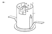
まず、本発明が適用される照明装置について簡単に説明する。図1及び図2において、1は装置本体で、この装置本体1は、アルミニウムのダイカスト製のもので、両端を開口した円筒状をしている。この装置本体1は、内部を仕切り部材1a、1bにより上下方向に3分割され、下方開口と仕切り部材1aの間の空間は、光源部2に形成されている。この光源部2には、半導体発光素子としての複数のLED2aと反射体2bが設けられている。複数のLED2aは、仕切り部材1a下面に設けられた円盤状の配線基板2cの円周方向に沿って等間隔に配置され実装されている。
(First embodiment)
First, a lighting device to which the present invention is applied will be briefly described. 1 and 2,
装置本体1の仕切り部材1aと1bの間の空間は電源室3に形成されている。この電源室3は、仕切り部材1a上部に配線基板3aが配置されている。この配線基板3aには、前記負荷としての複数のLED2aを駆動するための電源装置を構成する各電子部品が設けられている。この電源装置と複数のLED2aは、リード線4により接続されている。
A space between the
装置本体1の仕切り板1bと上方開口の間の空間は、電源端子室5に形成されている。この電源端子室5は、仕切り板1bに電源端子台6が設けられている。この電源端子台6は、電源室3の電源装置に商用電源の交流電力を供給するための端子台で、電絶縁性の合成樹脂で構成されたボックス6aの両面に電源ケーブル用端子部となる差込口6b、送りケーブル用端子部となる差込口6c及び電源線及び送り線を切り離すリリースボタン6dなどを有している。
A space between the
図3は、このような照明装置に適用されるスイッチングレギュレータより構成される電源装置の概略構成を示している。 FIG. 3 shows a schematic configuration of a power supply device configured by a switching regulator applied to such a lighting device.
図3において、10は電源本体で、この電源本体10には、交流電源11が接続されている。この交流電源11は、不図示の商用電源からなっている。この交流電源11には、全波整流回路12の入力端子が接続されている。全波整流回路12は、交流電源11からの交流電力を全波整流した出力を発生する。
In FIG. 3,
全波整流回路12には、電源手段として昇圧チョッパ回路13が接続されている。この昇圧チョッパ回路13は、全波整流回路12の正負極の出力端子間に昇圧用トランスを構成する第1のインダクタ14及びスイッチング素子としての電界効果トランジスタ15の直列回路が接続され、電界効果トランジスタ15に並列に図示極性のフライホイールダイオード16を介して平滑用コンデンサである電解コンデンサ17が接続されている。また、電解コンデンサ17の両端には、電圧検出手段として抵抗18,19の直列回路が接続されている。抵抗18,19は、電解コンデンサ17の出力より分圧電圧を発生し、このうち抵抗19の端子電圧を制御部27に出力する。電界効果トランジスタ15は、制御部27での、抵抗19の端子電圧と予め用意される参照電圧との比較結果に基づいてオンオフ動作される。第1のインダクタ14は、電界効果トランジスタ15のオンオフ動作に伴う電磁的エネルギーの蓄積及び放出によりフライホイールダイオード16を介して電解コンデンサ17に昇圧された出力を発生させる。制御部27については、後述する。
A
昇圧チョッパ回路13には、出力発生手段としての降圧チョッパ回路20が接続されている。この降圧チョッパ回路20は、電解コンデンサ17の両端にスイッチング素子としての電界効果トランジスタ21、フライホイールダイオード22及び負荷電流検出手段として抵抗23の直列回路が接続されている。また、フライホイールダイオード22には、第2のインダクタ24を介して接続手段を構成するコネクタ25が接続されている。コネクタ25については後述する。
The step-up
抵抗23は、後述するLEDモジュール29に流れる負荷電流を検出し、この検出出力を制御部27に出力する。電界効果トランジスタ21は、制御部27での、抵抗23より検出される負荷電流に応じた出力と予め用意される基準電圧との比較結果に基づいてオンオフ動作される。第2のインダクタ24は、電界効果トランジスタ21のオンオフ動作に伴う電磁的エネルギーの蓄積及び放出により後述する平滑コンデンサ26両端に降圧された直流出力を発生させる。
The
制御部27は、電源装置全体を制御するもので、電源出力制御部271と光出力制御部272を有している。電源出力制御部271は、予め不図示の参照電圧が記憶されていて、この参照電圧と抵抗19の端子電圧との比較結果に基づいて電界効果トランジスタ15のオンオフ動作を制御し、電界効果トランジスタ15のオンオフ動作に伴う第1のインダクタ14での電磁的エネルギーの蓄積及び放出により電解コンデンサ17両端に昇圧された出力電圧を発生させる。光出力制御部272は、予め基準値として不図示の基準電圧が用意されていて、この基準電圧と抵抗23より検出される負荷電流に応じた出力との比較結果に基づいて電界効果トランジスタ21をオンオフ動作させる。
The
コネクタ25は、図4に示すようなメス形コネクタからなるもので、ハウジング251内に3個の接続端子25a、25b、25cを有している。これら接続端子25a、25b、25cは、図3に示すように接続端子25aが第2のインダクタ24を介してフライホイールダイオード22のカソード端に、接続端子25cがフライホイールダイオード22のアノード端にそれぞれ接続され、また、接続端子25bと25cの間に、電解コンデンサからなる平滑コンデンサ26が接続されている。
The
コネクタ25には、接続手段を構成するコネクタ28を有する負荷としてのLEDモジュール29が着脱可能に接続される。コネクタ28は、図4に示すようなオス形コネクタからなるもので、ハウジング281内に、上述のコネクタ25の接続端子25a、25b、25cが各別に接続可能な3個の接続端子28a、28b、28cを有している。これら接続端子28a、28b、28cは、図3に示すように接続端子28a、28bの間が短絡され、これらの接続点と接続端子28cの間に、半導体発光素子として複数(図示例では4個)のLED素子291〜294が直列に接続されている。ここで、コネクタ28は、ハウジング281内において面積の大きな共通端子により短絡状態の接続端子28a、28bを構成するようにしてもよい。また、LEDモジュール29のLED素子291〜294が実装されるプリント基板(不図示)上に接続端子28a、28b間を短絡する配線を設けるようにしても良い。
An
なお、LEDモジュール29は、複数のLED素子を直列に接続した直列回路を、さらに複数個並列に接続したものであってもよい。
The
制御部27には、調光信号発生部30が接続されている。調光信号発生部30は、外部からの調光操作信号に基づいてデューティ比の異なるPWM信号を調光深度の異なる調光信号を発生し、この調光操作信号に基づいて制御部27で設定される基準電圧を可変してLEDモジュール29の光出力の調光を行う。
A
次に、このように構成した実施の形態の動作を説明する。 Next, the operation of the embodiment configured as described above will be described.
まず、電源本体10にLEDモジュール29を接続する場合は、図4に示すメス形のコネクタ25にオス形のコネクタ28を接続する。これらコネクタ25と28の接続により、フライホイールダイオード22の両端に、第2のインダクタ24、接続端子25a、28a、接続端子28b、25b、平滑コンデンサ26の直列回路が接続され、さらに平滑コンデンサ26の両端に接続端子25b、28b、接続端子25c、28cを介してLEDモジュール29のLED素子291〜294が接続される。
First, when the
この状態で、電源本体10の不図示の電源スイッチがオンされると、交流電源11の交流電力が全波整流回路12で全波整流され、昇圧チョッパ回路13に供給される。昇圧チョッパ回路13では、電源出力制御部271に予め用意された参照電圧と抵抗19の端子電圧との比較結果に基づいて電界効果トランジスタ15がオンオフ動作し、この電界効果トランジスタ15のオンオフ動作に伴う第1のインダクタ14の電磁的エネルギーの蓄積及び放出によりフライホイールダイオード16を介して電解コンデンサ17に昇圧された出力電圧を発生する。
In this state, when a power switch (not shown) of the power supply
昇圧チョッパ回路13の出力電圧は、降圧チョッパ回路20に供給される。降圧チョッパ回路20では、光出力制御部272に予め用意された基準電圧と抵抗23より検出される負荷電流に応じた出力との比較結果に基づいて電界効果トランジスタ21をオンオフ動作する。そして、この電界効果トランジスタ21のオンオフ動作に伴う第2のインダクタ24の電磁的エネルギーの蓄積及び放出により平滑コンデンサ26両端に降圧された直流電圧(直流出力)を発生し、この直流出力をLEDモジュール29のLED素子291〜294に供給し、これらLED素子291〜294の光出力を制御する。
The output voltage of the step-up
一方、電源本体10よりLEDモジュール29を取り外す場合は、図4に示すメス形のコネクタ25よりオス形のコネクタ28を切り離す。これにより、電源本体10よりLEDモジュール29が取り外され、同時に、平滑コンデンサ26も電源本体10から切り離される。
On the other hand, when the
このようにすれば、コネクタ25と28の間が確実に接続されていない場合は、平滑コンデンサ26が電源本体10から切り離されるので、仮に、コネクタ25と28の間の接続不良により負荷側が開放され、この状態で、電源本体10で電源投入され出力側に過電圧が発生することがあっても、このときの過電圧が平滑コンデンサ26に印加されることがなく、平滑コンデンサ26が耐圧を超えることで破損してしまうようなことを確実に防止できる。これにより、過電圧に対する平滑コンデンサ26の保護を確実に行うことができ、また、平滑コンデンサ26として、部品形状の大きくない、耐圧の低い通常のコンデンサを使用することができるので、コストアップの抑制を図ることもできる。
In this way, when the
また、平滑コンデンサ26の保護を目的とした専用の回路構成を設ける必要もないので、回路部品の増加もなく、電源装置の大型化やコストアップも抑制できる。
In addition, since it is not necessary to provide a dedicated circuit configuration for the purpose of protecting the smoothing
(変形例)
第1の実施の形態では、コネクタ25,28として、それぞれ3個の接続端子25a〜25c、28a〜28cを有するものについて述べたが、この変形例では、図5に示すように4個の接続端子31a〜31d、32a〜32dをそれぞれ有するコネクタ31、32を用いるようにしている。なお、電源本体10については図3で述べた構成と同様である。
(Modification)
In the first embodiment, the
この場合、コネクタ31は、接続端子31aが第2のインダクタ24を介してフライホイールダイオード22のカソード端に、接続端子31dがフライホイールダイオード22のアノード端にそれぞれ接続され、また、接続端子31bと31cの間に平滑コンデンサ26が接続されている。また、コネクタ32は、接続端子32aと32bの間と、接続端子32cと32dの間がそれぞれ短絡され、接続端子32aと32dの間にLEDモジュール29のLED素子291〜294が直列に接続されている。
In this case, the
このようにしても、電源本体10にLEDモジュール29を接続する場合、コネクタ31にコネクタ32を接続すると、平滑コンデンサ26が電源本体10に接続され、また、電源本体10よりLEDモジュール29を取り外す場合、コネクタ31よりコネクタ32を切り離すと、平滑コンデンサ26も電源本体10より切り離される。
Even in this case, when the
したがって、このようにしても、過電圧に対する平滑コンデンサ26の保護を確実に行うことができ、第1の実施の形態と同様な効果を得ることができる。
Therefore, even in this case, the smoothing
(第2の実施の形態)
図6は、本発明の第2の実施の形態を示すもので、図3と同一部分には、同符号を付している。この場合、電源本体10のフライホイールダイオード22には、第2のインダクタ24を介してインピーダンス素子としての補助コンデンサ33と平滑コンデンサ26の直列回路が接続されている。補助コンデンサ33は、電源本体10の出力側に過電圧が発生したとき、この過電圧を分圧して平滑コンデンサ26両端に耐圧以上の電圧が印加しないような容量のものに設定されている。
(Second Embodiment)
FIG. 6 shows a second embodiment of the present invention, and the same parts as those in FIG. In this case, a series circuit of an
これら補助コンデンサ33と平滑コンデンサ26に、接続手段を構成するコネクタ34が接続されている。コネクタ34は、メス形コネクタからなるもので、3個の接続端子34a、34b、34cを有している。これら接続端子34a、34b、34cは、接続端子34aが第2のインダクタ24と補助コンデンサ33の接続点に、接続端子34bが補助コンデンサ33と平滑コンデンサ26の接続点に、接続端子34cが平滑コンデンサ26とフライホイールダイオード22の接続点にそれぞれ接続されている。
The
また、コネクタ34には、接続手段を構成するコネクタ35を有するLEDモジュール29が着脱可能に接続される。コネクタ35は、オス形コネクタからなるもので、コネクタ34の接続端子34a、34b、34cに各別に接続可能な3個の接続端子35a、35b、35cを有している。これら接続端子35a、35b、35cは、接続端子35a、35bの間が短絡され、これらの接続点と接続端子35cの間に、LED素子291〜294が直列に接続されている。
Moreover, the
このような構成において、電源本体10にLEDモジュール29を接続する場合は、メス形のコネクタ34にオス形のコネクタ35を接続する。これらコネクタ34と35の接続により、接続端子34a、35a、接続端子35b、34bを介して補助コンデンサ33の両端が短絡され、フライホイールダイオード22の両端に、第2のインダクタ24を介して平滑コンデンサ26が接続され、さらに、平滑コンデンサ26の両端に接続端子34b、35b、接続端子34c、35cを介してLEDモジュール29のLED素子291〜294が接続される。
In such a configuration, when the
この状態で、電源本体10の不図示の電源スイッチがオンされると、交流電源11の交流電力が全波整流回路12で全波整流され、昇圧チョッパ回路13に供給される。昇圧チョッパ回路13では、上述したように電界効果トランジスタ15がオンオフ動作し、この電界効果トランジスタ15のオンオフ動作に伴う第1のインダクタ14の電磁的エネルギーの蓄積及び放出によりフライホイールダイオード16を介して電解コンデンサ17に昇圧された出力電圧を発生する。また、この出力電圧が降圧チョッパ回路20に供給されると、降圧チョッパ回路20でも、上述したように電界効果トランジスタ21をオンオフ動作し、この電界効果トランジスタ21のオンオフ動作に伴う第2のインダクタ24の電磁的エネルギーの蓄積及び放出により平滑コンデンサ26両端に降圧された直流電圧(直流出力)を発生し、この直流出力をLEDモジュール29のLED素子291〜294に供給し、これらLED素子291〜294の光出力を制御する。
In this state, when a power switch (not shown) of the power supply
一方、電源本体10よりLEDモジュール29を取り外す場合は、メス形のコネクタ34よりオス形のコネクタ35を切り離す。これにより、電源本体10よりLEDモジュール29が取り外される。また、コネクタ34とコネクタ35の切り離しにより、補助コンデンサ33の短絡が解かれ、補助コンデンサ33と平滑コンデンサ26の直列回路が電源本体10に接続される。
On the other hand, when the
このような構成において、例えば、コネクタ34と35の間が確実に接続されておらず、負荷側が開放された状態で、電源本体10で電源投入され、出力側に過電圧が発生すると、過電圧が補助コンデンサ33と平滑コンデンサ26の直列回路に印加される。この場合、補助コンデンサ33は、過電圧を分圧して平滑コンデンサ26側に耐圧以上の電圧が印加しないようにしている。これにより、過電圧が直接平滑コンデンサ26両端に印加されることがなくなり、平滑コンデンサ26が耐圧を超えることで破損してしまうようなことを確実に防止でき、過電圧に対する平滑コンデンサ26の保護を確実に行うことができるようになり、第1の実施の形態と同様な効果を得ることができる。
In such a configuration, for example, when the
(変形例)
第2の実施の形態では、コネクタ34,35として、それぞれ3個の接続端子34a〜34c、34a〜34cを有するものについて述べたが、この変形例では、図7に示すように4個の接続端子36a〜36d、37a〜37dをそれぞれ有するコネクタ36、37を用い、さらに2個の補助コンデンサ381、382を用いるようにしている。なお、電源本体10については図6で述べた構成と同様である。
(Modification)
In the second embodiment, the
この場合、電源本体10のフライホイールダイオード22には、第2のインダクタ24を介してインピーダンス素子としての補助コンデンサ381、平滑コンデンサ26及び他のインピーダンス素子としての補助コンデンサ382の直列回路が接続されている。これら補助コンデンサ381,382は、電源本体10の出力側に過電圧が発生したとき、この過電圧を分圧して平滑コンデンサ26両端に耐圧以上の電圧が印加しないような容量のものに設定されている。
In this case, a series circuit of an
コネクタ36は、接続端子36aが第2のインダクタ24と補助コンデンサ381の接続点に、接続端子36bが補助コンデンサ381と平滑コンデンサ26の接続点に、接続端子36cが平滑コンデンサ26と補助コンデンサ382の接続点に、接続端子36dが補助コンデンサ382とフライホイールダイオード22の接続点にそれぞれ接続されている。
The connector 36 has a
また、コネクタ37は、接続端子37aと37bの間、接続端子37cと37dの間がそれぞれ短絡され、接続端子37aと37dの間にLEDモジュール29のLED素子291〜294が直列に接続されている。
The
このようにしても、電源本体10にLEDモジュール29を接続する場合、コネクタ36にコネクタ37を接続すると、接続端子36a、37a、接続端子36b、37bを介して補助コンデンサ381が短絡され、接続端子36c、37c、接続端子36d、37dを介して補助コンデンサ382も短絡され、電源本体10には、平滑コンデンサ26が接続され、さらに、平滑コンデンサ26の両端に接続端子36b、37b、接続端子36c、37cを介してLEDモジュール29のLED素子291〜294が直列に接続されている。
Even in this case, when the
このようにしても、電源本体10にLEDモジュール29を接続する場合、コネクタ36にコネクタ37を接続すると、平滑コンデンサ26のみが電源本体10に接続され、また、電源本体10よりLEDモジュール29を取り外すとコネクタ36とコネクタ37の切り離しにより、補助コンデンサ381,382と平滑コンデンサ26の直列回路が電源本体10に接続される。これにより、電源本体10の出力側に過電圧が発生しても、補助コンデンサ381,382でのそれぞれの分圧により平滑コンデンサ26両端に耐圧以上の電圧が印加しないようできるので、過電圧に対する平滑コンデンサ26の保護を確実に行うことができ、第2の実施の形態と同様な効果を得ることができる。
Even in this case, when the
(第3の実施の形態)
図8は、本発明の第3の実施の形態を示すもので、図3と同一部分には、同符号を付している。この場合、電源本体10のフライホイールダイオード22には、第2のインダクタ24を介してインピーダンス素子としての比較的大きな抵抗値の抵抗素子39と平滑コンデンサ26の直列回路が接続されている。この場合、平滑コンデンサ26として用いられる電解コンデンサは等価的に並列抵抗体が存在するため、電源本体10の出力側に過電圧が発生すると、この過電圧により平滑コンデンサ26に大きな電流が流れようとする。この状態で、大きな抵抗値の抵抗素子39は、このときの電流を限流作用により抑制し、平滑コンデンサ26の両端電圧が耐圧以上にならないようにしている。
(Third embodiment)
FIG. 8 shows a third embodiment of the present invention, and the same parts as those in FIG. In this case, a series circuit of a smoothing
これら抵抗素子39と平滑コンデンサ26に、接続手段を構成するコネクタ40が接続されている。コネクタ40は、メス形コネクタからなるもので、3個の接続端子40a、40b、40cを有している。これら接続端子40a、40b、40cは、接続端子40aが第2のインダクタ24と抵抗素子39の接続点に、接続端子40bが抵抗素子39と平滑コンデンサ26の接続点に、接続端子40cがと平滑コンデンサ26とフライホイールダイオード22の接続点にそれぞれ接続されている。
A
また、コネクタ40には、接続手段を構成するコネクタ41を有するLEDモジュール29が着脱可能に接続される。コネクタ41は、オス形コネクタからなるもので、コネクタ40の接続端子40a、40b、40cに各別に接続可能な3個の接続端子41a、41b、41cを有している。これら接続端子41a、41b、41cは、接続端子41a、41bの間が短絡され、これらの接続点と接続端子41cの間に、LED素子291〜294が直列に接続されている。
Moreover, the
このような構成において、電源本体10にLEDモジュール29を接続する場合は、メス形のコネクタ40にオス形のコネクタ41を接続する。これらコネクタ40と41の接続により、接続端子40a、41a、接続端子41b、40bを介して抵抗素子39の両端が短絡され、フライホイールダイオード22の両端に、第2のインダクタ24を介して平滑コンデンサ26が接続され、さらに平滑コンデンサ26の両端に接続端子40b、41b、接続端子40c、41cを介してLEDモジュール29のLED素子291〜294が接続される。
In such a configuration, when the
この状態で、電源本体10の不図示の電源スイッチがオンされると、交流電源11の交流電力が全波整流回路12で全波整流され、昇圧チョッパ回路13に供給される。昇圧チョッパ回路13では、上述したように電界効果トランジスタ15がオンオフ動作し、この電界効果トランジスタ15のオンオフ動作に伴う第1のインダクタ14の電磁的エネルギーの蓄積及び放出によりフライホイールダイオード16を介して電解コンデンサ17に昇圧された出力電圧を発生する。また、この出力電圧が降圧チョッパ回路20に供給されると、降圧チョッパ回路20でも、上述したように電界効果トランジスタ21をオンオフ動作し、この電界効果トランジスタ21のオンオフ動作に伴う第2のインダクタ24の電磁的エネルギーの蓄積及び放出により平滑コンデンサ26両端に降圧された直流電圧(直流出力)を発生し、この直流出力をLEDモジュール29のLED素子291〜294に供給し、これらLED素子291〜294の光出力を制御する。
In this state, when a power switch (not shown) of the power supply
一方、電源本体10よりLEDモジュール29を取り外す場合は、メス形のコネクタ40よりオス形のコネクタ41を切り離す。これにより、電源本体10よりLEDモジュール29が取り外される。また、コネクタ40とコネクタ41の切り離しにより、抵抗素子39の短絡が解かれ、抵抗素子39と平滑コンデンサ26の直列回路が電源本体10に接続される。
On the other hand, when the
このような構成において、例えば、コネクタ40と41の間が確実に接続されておらず、負荷側が開放された状態で、電源本体10で電源投入され、出力側に過電圧が発生すると、過電圧が抵抗素子39と平滑コンデンサ26の直列回路に印加される。この場合、抵抗素子39は、過電圧により平滑コンデンサ26に流れようとする大きな電流を限流作用により抑制し、平滑コンデンサ26側に耐圧以上の電圧が印加しないようにしている。これにより、過電圧により平滑コンデンサ26両端に耐圧以上の電圧が加わり、平滑コンデンサ26を破損してしまうようなことを確実に防止でき、過電圧に対する平滑コンデンサ26の保護を確実に行うことができるようになり、第1の実施の形態と同様な効果を得ることができる。
In such a configuration, for example, when the
(変形例)
第3の実施の形態では、コネクタ40,41として、それぞれ3個の接続端子40a〜40c、41a〜41cを有するものについて述べたが、この変形例では、図9に示すように4個の接続端子43a〜43d、44a〜44dをそれぞれ有するコネクタ43、44を用い、さらに2個の抵抗素子421、422を用いるようにしている。なお、電源本体10については図8で述べた構成と同様である。
(Modification)
In the third embodiment, the
この場合、電源本体10のフライホイールダイオード22には、第2のインダクタ24を介してインピーダンス素子としての抵抗素子421、平滑コンデンサ26及び他のインピーダンス素子としての抵抗素子422の直列回路が接続されている。これら抵抗素子421、422は、電源本体10の出力側に過電圧が発生したとき、過電圧により平滑コンデンサ26に流れる電流を限流作用により抑制し、平滑コンデンサ26側に耐圧以上の電圧が印加しないような比較的大きな抵抗値のものが用いられる。
In this case, a series circuit of a
コネクタ43は、接続端子43aが第2のインダクタ24と抵抗素子421の接続点に、接続端子43bが抵抗素子421と平滑コンデンサ26の接続点に、接続端子43cが平滑コンデンサ26と抵抗素子422の接続点に、接続端子43dが抵抗素子422とフライホイールダイオード22の接続点にそれぞれ接続されている。
The
また、コネクタ44は、接続端子44aと44bの間、接続端子44cと44dの間がそれぞれ短絡され、接続端子44aと44dの間にLEDモジュール29のLED素子291〜294が直列に接続されている。
The
このようにしても、電源本体10にLEDモジュール29を接続する場合、コネクタ43にコネクタ44を接続すると、接続端子43a、44a、接続端子43b、44bを介して抵抗素子421が短絡され、接続端子43c、44c、接続端子43d、44dを介して抵抗素子422も短絡され、電源本体10には、平滑コンデンサ26のみが接続され、さらに、平滑コンデンサ26の両端に接続端子43b、44b、接続端子43c、44cを介してLEDモジュール29のLED素子291〜294が直列に接続される。
Even in this case, when the
このようにしても、電源本体10にLEDモジュール29を接続する場合、コネクタ43にコネクタ44を接続すると、平滑コンデンサ26のみが電源本体10に接続され、また、電源本体10よりLEDモジュール29を取り外すとコネクタ43とコネクタ44の切り離しにより、抵抗素子421,422と平滑コンデンサ26の直列回路が電源本体10に接続される。これにより、電源本体10の出力側に過電圧が発生しても抵抗素子421、422のそれぞれの限流作用により平滑コンデンサ26に耐圧以上の電圧が印加しないようにできるので、過電圧に対する平滑コンデンサ26の保護を確実に行うことができ、第2の実施の形態と同様な効果を得ることができる。
Even in this case, when the
なお、本発明は、上記実施の形態に限定されるものでなく、実施段階では、その要旨を変更しない範囲で種々変形することが可能である。例えば、上述した実施の形態では、制御部は、アナログ回路の例を述べたが、マイコンやデジタル処理を用いた制御方式を採用したものを用いることができる。また、上述した実施の形態では、負荷として、LED素子291〜294を有するLEDモジュール29の場合を述べたが、放電灯などの他の負荷も適用することができる。
In addition, this invention is not limited to the said embodiment, In the implementation stage, it can change variously in the range which does not change the summary. For example, in the above-described embodiment, an example of an analog circuit is described as the control unit, but a control unit using a microcomputer or digital processing can be used. In the above-described embodiment, the case of the
さらに、上記実施の形態には、種々の段階の発明が含まれており、開示されている複数の構成要件における適宜な組み合わせにより種々の発明が抽出できる。例えば、実施の形態に示されている全構成要件から幾つかの構成要件が削除されても、発明が解決しようとする課題の欄で述べた課題を解決でき、発明の効果の欄で述べられている効果が得られる場合には、この構成要件が削除された構成が発明として抽出できる。 Furthermore, the above embodiments include inventions at various stages, and various inventions can be extracted by appropriately combining a plurality of disclosed constituent elements. For example, even if some constituent requirements are deleted from all the constituent requirements shown in the embodiment, the problem described in the column of the problem to be solved by the invention can be solved, and is described in the column of the effect of the invention. If the above effect is obtained, a configuration from which this configuration requirement is deleted can be extracted as an invention.
1…装置本体、2…光源部、3…電源室、
10…電源本体、11…交流電源
12…全波整流回路、13…昇圧チョッパ回路
20…降圧チョッパ回路、25.28…コネクタ
26…平滑コンデンサ、27…制御部、29…LEDモジュール
291〜294…LED素子、31.32…コネクタ
33、381.382…補助コンデンサ
31.32、34.35、36.37…コネクタ
39、421.422…抵抗素子
40.41、43.44…コネクタ
DESCRIPTION OF
DESCRIPTION OF
Claims (6)
少なくとも3つの端子を有する電源側接続手段と;
を具備し、
モジュールは、モジュール側接続手段と、発光素子とを備え、前記モジュール側接続手段は、前記電源側接続手段の少なくとも3つの端子にそれぞれ接続する接続端子を有し、前記発光素子は、前記モジュール側接続手段の接続端子のいずれか2つに接続することを特徴とし、前記電源側接続手段の少なくとも3つの端子は、それぞれ前記電源本体の一対の出力端および前記電源本体の平滑コンデンサの一端のいずれかに接続されるとともに、前記電源本体の一対の出力端のいずれかと前記電源本体の平滑コンデンサの一端とは、前記電源側接続手段の2つの端子および前記モジュール側接続手段の2つの接続端子を介して電気的に接続されることを特徴とする照明装置。 A switching element, a smoothing capacitor that generates a DC output supplied to a load by an on / off operation of the switching element, and a power source body having a pair of output ends;
Power supply side connection means having at least three terminals;
Comprising
The module includes a module side connection means and a light emitting element, and the module side connection means has connection terminals respectively connected to at least three terminals of the power supply side connection means, and the light emitting element is connected to the module side. It is connected to any two of the connection terminals of the connection means, and at least three terminals of the power supply side connection means are either one of a pair of output terminals of the power supply body and one end of a smoothing capacitor of the power supply body. One of the pair of output ends of the power supply body and one end of the smoothing capacitor of the power supply body are connected to two terminals of the power supply side connection means and two connection terminals of the module side connection means. A lighting device that is electrically connected to each other.
前記電源本体の平滑コンデンサの他端および前記電源本体の一対の出力端の他方との間に接続される第2補助コンデンサと、
を具備することを特徴とする請求項2記載の照明装置。 A first auxiliary capacitor connected between one end of the smoothing capacitor of the power source body and one of the pair of output ends of the power source body;
A second auxiliary capacitor connected between the other end of the smoothing capacitor of the power source body and the other of the pair of output ends of the power source body;
The lighting device according to claim 2, further comprising:
前記電源本体の平滑コンデンサの他端および前記電源本体の一対の出力端の他方との間に接続される第2インピーダンス素子と、
を具備することを特徴とする請求項2記載の照明装置。 A first impedance element connected between one end of the smoothing capacitor of the power source body and one of the pair of output ends of the power source body;
A second impedance element connected between the other end of the smoothing capacitor of the power supply body and the other of the pair of output terminals of the power supply body;
The lighting device according to claim 2, further comprising:
Priority Applications (1)
| Application Number | Priority Date | Filing Date | Title |
|---|---|---|---|
| JP2009113631A JP5682742B2 (en) | 2009-05-08 | 2009-05-08 | Power supply device and lighting device |
Applications Claiming Priority (1)
| Application Number | Priority Date | Filing Date | Title |
|---|---|---|---|
| JP2009113631A JP5682742B2 (en) | 2009-05-08 | 2009-05-08 | Power supply device and lighting device |
Publications (2)
| Publication Number | Publication Date |
|---|---|
| JP2010263716A JP2010263716A (en) | 2010-11-18 |
| JP5682742B2 true JP5682742B2 (en) | 2015-03-11 |
Family
ID=43361337
Family Applications (1)
| Application Number | Title | Priority Date | Filing Date |
|---|---|---|---|
| JP2009113631A Expired - Fee Related JP5682742B2 (en) | 2009-05-08 | 2009-05-08 | Power supply device and lighting device |
Country Status (1)
| Country | Link |
|---|---|
| JP (1) | JP5682742B2 (en) |
Families Citing this family (10)
| Publication number | Priority date | Publication date | Assignee | Title |
|---|---|---|---|---|
| KR101040833B1 (en) | 2011-04-05 | 2011-06-14 | 김성윤 | Ballast circuit for LED lighting |
| JP5967511B2 (en) * | 2010-12-20 | 2016-08-10 | パナソニックIpマネジメント株式会社 | LED lighting device and lighting apparatus using the same |
| KR101920296B1 (en) * | 2011-01-26 | 2018-11-21 | 페어차일드코리아반도체 주식회사 | Switch control circuit, switch controlling method, and power supply device using the switch control circuit |
| JP5972557B2 (en) * | 2011-11-28 | 2016-08-17 | ローム株式会社 | LED driver module and LED bulb using the same |
| JP5188643B1 (en) * | 2012-08-23 | 2013-04-24 | 株式会社共進電機製作所 | Power supply |
| EP2709426A3 (en) | 2012-09-14 | 2017-04-19 | Panasonic Intellectual Property Management Co., Ltd. | Solid-state light-emitting element drive device, lighting system and lighting fixture |
| JP6173042B2 (en) * | 2013-05-24 | 2017-08-02 | 三菱電機株式会社 | Light source lighting device and lighting device |
| JP6172460B2 (en) * | 2013-12-17 | 2017-08-02 | 東芝ライテック株式会社 | Lamp device, socket and lighting device |
| KR101547480B1 (en) * | 2014-08-20 | 2015-08-26 | 유상우 | Apparatus for driving LED |
| CN112483524B (en) * | 2019-09-12 | 2022-12-16 | 喜利得股份公司 | Expansion anchor bolt |
Family Cites Families (3)
| Publication number | Priority date | Publication date | Assignee | Title |
|---|---|---|---|---|
| JPH054278U (en) * | 1991-04-04 | 1993-01-22 | 三菱電機株式会社 | Hot-swapping circuit for IC card |
| JP4761201B2 (en) * | 2005-10-31 | 2011-08-31 | 株式会社安川電機 | Power converter |
| JP2008124008A (en) * | 2006-10-18 | 2008-05-29 | Nobuichi Tsubota | LED unit, LED unit manufacturing method, and ceiling lighting apparatus using the LED unit |
-
2009
- 2009-05-08 JP JP2009113631A patent/JP5682742B2/en not_active Expired - Fee Related
Also Published As
| Publication number | Publication date |
|---|---|
| JP2010263716A (en) | 2010-11-18 |
Similar Documents
| Publication | Publication Date | Title |
|---|---|---|
| JP5682742B2 (en) | Power supply device and lighting device | |
| US9883555B2 (en) | Ballast-compatible lighting driver and light emitting diode lamp comprising the same | |
| US10663130B2 (en) | Lighting arrangement with battery backup | |
| CN211297077U (en) | Detection circuit for installation state | |
| CN210444530U (en) | Install the detection module, the power module and the LED straight tube light using the modules | |
| EP2741583B1 (en) | Lighting device and luminaire including the same | |
| JP2008243619A (en) | LED lighting device | |
| JP6692069B2 (en) | Power supply and lighting device | |
| JP5169159B2 (en) | DC power supply | |
| JP6777183B2 (en) | lighting equipment | |
| KR101325781B1 (en) | D.c. power supply having detachable mounting mechanism of electrolytic capacitors | |
| JP6473994B2 (en) | lighting equipment | |
| JP2015088344A (en) | Backup power supply for power failure lamp, and power failure lamp unit | |
| JP2019061803A (en) | Luminaire | |
| US20160276938A1 (en) | Power Converter | |
| JP6883762B2 (en) | Power supply and lighting | |
| JP2012022881A (en) | Power supply device and lighting system | |
| JP5476212B2 (en) | POWER SUPPLY DEVICE AND LIGHTING DEVICE USING THE SAME | |
| JP6840997B2 (en) | Lighting equipment and lighting equipment | |
| AU2019201725B2 (en) | Printed circuit board arrangement for welding and cutting apparatus | |
| JP2013134844A (en) | Light source lighting device and luminaire | |
| JP2014531736A (en) | LED lighting equipment | |
| CN219659954U (en) | LED product and constant current driving source thereof | |
| JP7357199B2 (en) | Lighting devices, light source units and lighting fixtures | |
| KR102260295B1 (en) | LED module power supply converter with PCB pattern-connected surge voltage protection circuit |
Legal Events
| Date | Code | Title | Description |
|---|---|---|---|
| A621 | Written request for application examination |
Free format text: JAPANESE INTERMEDIATE CODE: A621 Effective date: 20120228 |
|
| A977 | Report on retrieval |
Free format text: JAPANESE INTERMEDIATE CODE: A971007 Effective date: 20130628 |
|
| A131 | Notification of reasons for refusal |
Free format text: JAPANESE INTERMEDIATE CODE: A131 Effective date: 20130702 |
|
| RD02 | Notification of acceptance of power of attorney |
Free format text: JAPANESE INTERMEDIATE CODE: A7422 Effective date: 20130807 |
|
| A521 | Request for written amendment filed |
Free format text: JAPANESE INTERMEDIATE CODE: A523 Effective date: 20130902 |
|
| RD07 | Notification of extinguishment of power of attorney |
Free format text: JAPANESE INTERMEDIATE CODE: A7427 Effective date: 20140205 |
|
| A521 | Request for written amendment filed |
Free format text: JAPANESE INTERMEDIATE CODE: A821 Effective date: 20140205 |
|
| A02 | Decision of refusal |
Free format text: JAPANESE INTERMEDIATE CODE: A02 Effective date: 20140311 |
|
| A521 | Request for written amendment filed |
Free format text: JAPANESE INTERMEDIATE CODE: A523 Effective date: 20140611 |
|
| A911 | Transfer to examiner for re-examination before appeal (zenchi) |
Free format text: JAPANESE INTERMEDIATE CODE: A911 Effective date: 20140619 |
|
| A131 | Notification of reasons for refusal |
Free format text: JAPANESE INTERMEDIATE CODE: A131 Effective date: 20140819 |
|
| A521 | Request for written amendment filed |
Free format text: JAPANESE INTERMEDIATE CODE: A523 Effective date: 20141017 |
|
| A131 | Notification of reasons for refusal |
Free format text: JAPANESE INTERMEDIATE CODE: A131 Effective date: 20141127 |
|
| A521 | Request for written amendment filed |
Free format text: JAPANESE INTERMEDIATE CODE: A523 Effective date: 20141127 |
|
| TRDD | Decision of grant or rejection written | ||
| A01 | Written decision to grant a patent or to grant a registration (utility model) |
Free format text: JAPANESE INTERMEDIATE CODE: A01 Effective date: 20141217 |
|
| A61 | First payment of annual fees (during grant procedure) |
Free format text: JAPANESE INTERMEDIATE CODE: A61 Effective date: 20141230 |
|
| R151 | Written notification of patent or utility model registration |
Ref document number: 5682742 Country of ref document: JP Free format text: JAPANESE INTERMEDIATE CODE: R151 |
|
| LAPS | Cancellation because of no payment of annual fees |