JP5633105B2 - Light source device and liquid crystal display device - Google Patents
Light source device and liquid crystal display device Download PDFInfo
- Publication number
- JP5633105B2 JP5633105B2 JP2008273592A JP2008273592A JP5633105B2 JP 5633105 B2 JP5633105 B2 JP 5633105B2 JP 2008273592 A JP2008273592 A JP 2008273592A JP 2008273592 A JP2008273592 A JP 2008273592A JP 5633105 B2 JP5633105 B2 JP 5633105B2
- Authority
- JP
- Japan
- Prior art keywords
- light
- light emitting
- light source
- source device
- layer
- Prior art date
- Legal status (The legal status is an assumption and is not a legal conclusion. Google has not performed a legal analysis and makes no representation as to the accuracy of the status listed.)
- Expired - Fee Related
Links
Images


Classifications
-
- H—ELECTRICITY
- H10—SEMICONDUCTOR DEVICES; ELECTRIC SOLID-STATE DEVICES NOT OTHERWISE PROVIDED FOR
- H10K—ORGANIC ELECTRIC SOLID-STATE DEVICES
- H10K59/00—Integrated devices, or assemblies of multiple devices, comprising at least one organic light-emitting element covered by group H10K50/00
- H10K59/80—Constructional details
- H10K59/875—Arrangements for extracting light from the devices
- H10K59/879—Arrangements for extracting light from the devices comprising refractive means, e.g. lenses
-
- H—ELECTRICITY
- H10—SEMICONDUCTOR DEVICES; ELECTRIC SOLID-STATE DEVICES NOT OTHERWISE PROVIDED FOR
- H10K—ORGANIC ELECTRIC SOLID-STATE DEVICES
- H10K59/00—Integrated devices, or assemblies of multiple devices, comprising at least one organic light-emitting element covered by group H10K50/00
- H10K59/80—Constructional details
- H10K59/875—Arrangements for extracting light from the devices
- H10K59/877—Arrangements for extracting light from the devices comprising scattering means
Landscapes
- Diffracting Gratings Or Hologram Optical Elements (AREA)
- Liquid Crystal (AREA)
- Electroluminescent Light Sources (AREA)
- Planar Illumination Modules (AREA)
Description
本発明は、光源装置及び液晶表示装置に関する。 The present invention relates to a light source device and a liquid crystal display device.
複数層の電極間に有機発光層を設け、電気的に発光を得る有機エレクトロルミネッセンス(以下「有機EL」と略す場合がある。)素子は、液晶セルに代わる表示素子としての利用の他に、その高発光効率、低電圧駆動、軽量、低コスト等の特徴を生かした、平面型照明、液晶表示装置用バックライト等の面光源としての利用も検討されている。 In addition to use as a display element in place of a liquid crystal cell, an organic electroluminescence (hereinafter sometimes abbreviated as “organic EL”) element that provides an organic light-emitting layer between a plurality of layers of electrodes to obtain light emission is used. Utilization as a surface light source such as a flat-type illumination and a backlight for a liquid crystal display device utilizing the features such as high luminous efficiency, low voltage drive, light weight, and low cost is also being studied.
有機EL素子を面光源として利用する場合、その光取り出し効率を高めることが課題となる。すなわち、有機EL素子の発光層自体は発光効率が高いものの、それが光源装置を構成する積層構造を透過して出光するまでの間に、層中における干渉等により光量が低減してしまうので、そのような光の損失を可能な限り低減することが求められる。光取り出し効率を高めるための方法として、例えば特許文献1には、素子の正面方向(0°)の輝度を抑制し、角度50〜70°の輝度を増加させることで、全体的な輝度を高めることが開示されている。
When an organic EL element is used as a surface light source, it is a problem to increase the light extraction efficiency. That is, although the light emitting layer itself of the organic EL element has high luminous efficiency, the light amount is reduced due to interference or the like in the layer until it emits light through the laminated structure constituting the light source device. It is required to reduce such light loss as much as possible. As a method for increasing the light extraction efficiency, for example, in
有機EL素子においては、自然光に近い光を得るために、2種以上の発光素子を用い2以上の発光ピークを有する光を出射させることがある。このような有機EL素子を面光源に用いる場合、光取り出し効率の向上に加えて、観察角度による色味の変化を低減することが、さらなる課題となる。即ち、前述の層中における干渉の発生のしかたは、光の波長によって異なるため、各ピークの配光特性に違いが生じ、その結果、面光源を正面方向から観察した場合と、斜め方向から観察する場合とで、観察角度による色味の変化が発生し、光源として好ましくないものとなってしまう。 In an organic EL element, in order to obtain light close to natural light, light having two or more emission peaks may be emitted using two or more types of light emitting elements. When such an organic EL element is used as a surface light source, in addition to improving light extraction efficiency, it is a further problem to reduce a change in color depending on an observation angle. In other words, since the manner of occurrence of interference in the above-mentioned layers differs depending on the wavelength of light, there is a difference in the light distribution characteristics of each peak, and as a result, the surface light source is observed from the front and the oblique light is observed. In this case, a change in color depending on the observation angle occurs, which is not preferable as a light source.
本発明の目的は、観察角度による色味の変化が抑制された光源装置及び液晶表示装置を提供することにある。 An object of the present invention is to provide a light source device and a liquid crystal display device in which a change in color depending on an observation angle is suppressed.
上記課題を解決するために本願発明者らは検討を行った結果、光源装置において、有機EL光源素子等の発光素子と、特定の回折素子とを組み合わせることにより、上記課題を解決しうることを見出し、本願発明を解決するに至った。
したがって、本発明によれば、下記〔1〕〜〔6〕が提供される。
The inventors of the present application have studied to solve the above problems, and as a result, in the light source device, by combining a light emitting element such as an organic EL light source element and a specific diffraction element, the above problem can be solved. The headline and the present invention have been solved.
Therefore, according to the present invention, the following [1] to [6] are provided.
〔1〕 ピーク波長がλ1である第1の発光ピーク、及びピーク波長がλ2である第2の発光ピークを有する発光素子と、前記発光素子の出光側に設けられた回折素子とを備え、
前記回折素子から出光する光の波長λ1における配光特性と波長λ2における配光特性との差が、前記発光素子の波長λ1における配光特性と波長λ2における配光特性との差よりも小さい光源装置。
〔2〕 〔1〕に記載の光源装置であって、
前記発光素子から出光する光の波長λ1(nm)の正面方向の強度を1とした際の極角60°方向の相対強度RA1、
前記発光素子から出光する光の波長λ2(nm)の正面方向の強度を1とした際の極角60°方向の相対強度RA2、
前記回折素子から出光する光の波長λ1(nm)の正面方向の強度を1とした際の極角60°方向の相対強度RB1、及び
前記回折素子から出光する光の波長λ2(nm)の正面方向の強度を1とした際の極角60°方向の相対強度RB2が、式(1):
|RA1−RA2|>|RB1−RB2| ・・・式(1)
の関係を満たす光源装置。
〔3〕 〔1〕又は〔2〕に記載の光源装置であって、
前記回折素子が、ピッチが300〜4000nmの第1の凹凸形状を有する光源装置。
〔4〕 〔3〕に記載の光源装置であって、
前記回折素子が、前記第1の凹凸形状より大きいピッチを有する第2の凹凸形状をさらに有し、
前記第1の凹凸形状が、前記第2の凹凸形状を構成する面上に設けられている光源装置。
〔5〕 〔1〕〜〔4〕のいずれか1項に記載の光源装置であって、
前記発光素子の出光側に設けられた、拡散層をさらに有する光源装置。
〔6〕 〔1〕〜〔5〕のいずれか1項に記載の光源装置を備える液晶表示装置。
[1] A light emitting device having a first light emission peak having a peak wavelength of λ1 and a second light emission peak having a peak wavelength of λ2, and a diffraction device provided on the light output side of the light emitting device,
A light source in which the difference between the light distribution characteristic at the wavelength λ1 and the light distribution characteristic at the wavelength λ2 of the light emitted from the diffraction element is smaller than the difference between the light distribution characteristic at the wavelength λ1 and the light distribution characteristic at the wavelength λ2 of the light emitting element. apparatus.
[2] The light source device according to [1],
Relative intensity RA1 in the polar angle direction of 60 ° when the intensity in the front direction of the wavelength λ1 (nm) of the light emitted from the light emitting element is 1.
The relative intensity RA2 in the
Relative intensity RB1 in the polar angle direction of 60 ° when the intensity in the front direction of the wavelength λ1 (nm) of the light emitted from the diffractive element is 1, and the front of the wavelength λ2 (nm) of the light emitted from the diffractive element The relative intensity RB2 in the direction of the polar angle of 60 ° when the direction intensity is set to 1 is the formula (1):
| RA1-RA2 |> | RB1-RB2 | Formula (1)
Light source device that satisfies the relationship.
[3] The light source device according to [1] or [2],
The light source device in which the diffraction element has a first uneven shape with a pitch of 300 to 4000 nm.
[4] The light source device according to [3],
The diffractive element further has a second concavo-convex shape having a pitch larger than the first concavo-convex shape,
The light source device in which the first uneven shape is provided on a surface constituting the second uneven shape.
[5] The light source device according to any one of [1] to [4],
A light source device further including a diffusion layer provided on a light output side of the light emitting element.
[6] A liquid crystal display device comprising the light source device according to any one of [1] to [5].
本発明の光源装置は、観察角度による色味の変化が少ないため、液晶表示装置のバックライト、照明装置などの光源として有用である。
特に前記〔4]に係る光源装置は、第2の凹凸形状による光学的効果を得ながら、且つ観察角度による色味の変化をさらに低減することができる。
また、特に前記〔5〕に係る光源装置は、輝度の低下、光源装置の厚さや重量の増加などの不所望な効果を発現することなく、観察角度による色味の変化をより良好に改善することができる。
本発明の液晶表示装置は、前記本発明の光源装置を備えることにより、観察角度による色味の変化が少ない表示装置とすることができる。
The light source device of the present invention is useful as a light source for a backlight of a liquid crystal display device, an illuminating device, and the like because there is little change in color depending on the viewing angle.
In particular, the light source device according to [4] can further reduce the change in color depending on the observation angle while obtaining the optical effect of the second uneven shape.
In particular, the light source device according to the above [5] better improves the change in color depending on the observation angle without exhibiting undesirable effects such as a decrease in luminance and an increase in the thickness and weight of the light source device. be able to.
By providing the light source device of the present invention, the liquid crystal display device of the present invention can be a display device with little change in color depending on the observation angle.
以下、本発明の好ましい実施形態を、図面を参照して説明する。 Hereinafter, preferred embodiments of the present invention will be described with reference to the drawings.
(第1実施形態)
図1は、本発明の第1の実施形態に係る光源装置を概略的に示す断面図である。図1に示すように、光源装置100は、発光素子120と、発光素子120の出光側に設けられる基板101と、基板101の出光側に設けられる回折素子1とを備える。したがって、回折素子1は、発光素子120の出光側に配置されている。
基板101は、光入射側の面101Aと、光出射側の面101Bとを備えている。
発光素子120は、基板101の一方の面101Aに接して設けられる透明電極111と、発光層121と、反射電極112とをこの順に備える。発光素子120において、透明電極111及び反射電極112間に電圧を印加すると、発光層121から光が発生する。この発生した光は、直接または反射電極112で反射されてから透明電極111に入射し、透明電極111から出光する。したがって、本実施形態では、発光素子120より図中の上側が、発光素子の出光側となる。
(First embodiment)
FIG. 1 is a cross-sectional view schematically showing a light source device according to the first embodiment of the present invention. As shown in FIG. 1, the
The
The
回折素子1は、基板101の、発光素子120が設けられている面101Aとは反対側の面101B上に設けられている。回折素子1は、回折素子の基板20と、基板20の出光面109上に形成された、複数の凸部2からなる回折構造体22とを備え、この回折構造体22により、回折素子としての機能を発揮する。
The
(発光素子)
本発明において、発光素子は、ピーク波長がλ1である第1の発光ピーク、及びピーク波長がλ2である第2の発光ピークを有する。ここで、λ1とはλ2とは異なる波長である。λ1とλ2との関係は、特に限定されないが、例えばその差(|λ1−λ2|)を、好ましくは10〜500nm、より好ましくは25〜300nmとすることができる。発光素子の発光ピークの数は2に限られず、3以上の数を有することもできる。光源装置において発光素子が3以上の発光ピークを有する場合、それらのうちの2つを第1及び第2の発光ピークとした場合に本発明の要件を充足する装置を、本発明の光源装置とすることができ、3以上の発光ピークのどれを第1及び第2の発光ピークとした場合にも本発明の要件を充足することがさらに好ましい。
(Light emitting element)
In the present invention, the light emitting element has a first emission peak with a peak wavelength of λ1 and a second emission peak with a peak wavelength of λ2. Here, λ1 is a wavelength different from λ2. The relationship between λ1 and λ2 is not particularly limited. For example, the difference (| λ1-λ2 |) can be preferably 10 to 500 nm, more preferably 25 to 300 nm. The number of light emission peaks of the light emitting element is not limited to 2 and may be 3 or more. When the light emitting element has three or more light emission peaks in the light source device, a device that satisfies the requirements of the present invention when two of them are the first and second light emission peaks is referred to as the light source device of the present invention. It is more preferable that the requirement of the present invention is satisfied when any of the three or more emission peaks is the first and second emission peaks.
かかる発光素子の好適な例としては、複数の発光材料を含む発光層を有する有機EL発光素子を挙げることができる。 As a preferable example of such a light emitting element, an organic EL light emitting element having a light emitting layer containing a plurality of light emitting materials can be given.
有機EL発光素子を構成する発光層としては、特に限定されず既知のものを適宜選択することができるが、光源としての用途に適合すべく、一層単独又は複数の層の組み合わせにより、第1及び第2の発光ピークを含む光を発光するものとすることができる。 The light-emitting layer constituting the organic EL light-emitting element is not particularly limited and can be appropriately selected from known ones. However, in order to suit the use as a light source, a single layer or a combination of a plurality of layers can be used. Light including the second emission peak can be emitted.
発光素子は、さらに電極を含むことができ、これらは特に限定されず有機EL素子に用いられる既知のものを適宜選択することができる。具体的には例えば透明電極及び反射電極の対を有し、透明電極側を出光側とすることができる。発光素子はさらに、電極間に、発光層に加えてホール注入層、ホール輸送層、電子輸送層、電子注入層及びガスバリア層等の他の層を有することもできる。 The light emitting element can further include an electrode, and these are not particularly limited, and known elements used for the organic EL element can be appropriately selected. Specifically, for example, a pair of a transparent electrode and a reflective electrode is provided, and the transparent electrode side can be the light output side. The light-emitting element can further include other layers such as a hole injection layer, a hole transport layer, an electron transport layer, an electron injection layer, and a gas barrier layer in addition to the light-emitting layer between the electrodes.
発光素子の具体的な層構成としては、陽極/正孔輸送層/発光層/陰極の構成、陽極/正孔輸送層/発光層/電子注入層/陰極の構成、陽極/正孔注入層/発光層/陰極の構成、陽極/正孔注入層/正孔輸送層/発光層/電子輸送層/電子注入層/陰極の構成、陽極/正孔輸送層/発光層/電子注入層/等電位面形成層/正孔輸送層/発光層/電子注入層/陰極の構成,陽極/正孔輸送層/発光層/電子注入層/電荷発生層/正孔輸送層/発光層/電子注入層/陰極の構成などが挙げられる。 Specific layer configurations of the light-emitting element include anode / hole transport layer / light-emitting layer / cathode configuration, anode / hole transport layer / light-emitting layer / electron injection layer / cathode configuration, anode / hole injection layer / Composition of light emitting layer / cathode, anode / hole injection layer / hole transport layer / light emitting layer / electron transport layer / electron injection layer / cathode composition, anode / hole transport layer / light emitting layer / electron injection layer / equipotential Structure of surface forming layer / hole transport layer / light emitting layer / electron injection layer / cathode, anode / hole transport layer / light emitting layer / electron injection layer / charge generation layer / hole transport layer / light emitting layer / electron injection layer / Examples include the configuration of the cathode.
複数の発光ピークを含む光を発光するために、本発明の光源装置は、上記のような層構成を有する発光素子を2以上有し、それぞれが第1及び第2の発光ピークを有するものとすることができる。また、1つのみの発光素子を有し、その中に発光材料を複数有するものとすることもできる。1つの発光素子が複数の発光材料を有する場合は、1対の陽極と陰極との間に発光色が異なる複数層の発光層を有することもでき、1層の発光層のみを有し、その中においてある色素に異なる色素がドーピングされていてもよい。 In order to emit light including a plurality of emission peaks, the light source device of the present invention has two or more light emitting elements having the above-described layer configuration, each having a first and second emission peaks. can do. It is also possible to have only one light emitting element and a plurality of light emitting materials therein. When one light-emitting element has a plurality of light-emitting materials, it can have a plurality of light-emitting layers with different emission colors between a pair of anode and cathode, and has only one light-emitting layer, A different dye may be doped in a certain dye.
発光素子を構成する各層の材料は特に限定されず、任意の既知の材料を用いうる。例えば発光材料としてはポリパラフェニレンビニレン系・ポリフルオレン系・ポリビニルカルバゾール系の材料を挙げることができ、第1及び第2の発光ピークに対応する2種以上の発光材料を用いて、1層又は2層以上の発光層を構成することができる。また正孔注入層や正孔輸送層としてはフタロシアニン系・アリールアミン系・ポリチオフェン系、電子注入層や電子輸送層にはアルミ錯体・フッ化リチウムなどがあげられる。また、透電位面形成層、あるいは電荷発生層としては、ITO、IZO、SnO2などの透明電極、あるいはAg,Alなどの金属薄膜があげられる。 The material of each layer constituting the light-emitting element is not particularly limited, and any known material can be used. For example, examples of the light-emitting material include polyparaphenylene vinylene-based, polyfluorene-based, and polyvinyl carbazole-based materials. One or more layers can be formed using two or more light-emitting materials corresponding to the first and second emission peaks. Two or more light emitting layers can be formed. Examples of the hole injection layer and the hole transport layer include phthalocyanine-based, arylamine-based, and polythiophene-based materials, and examples of the electron injection layer and the electron transport layer include aluminum complexes and lithium fluoride. As the magnetic potential surface forming layer or the charge generation layer, ITO, IZO, the transparent electrode such as SnO 2, or Ag, a metal thin film such as Al and the like.
発光素子を基板上に形成する場合、基板としては、ガラス基板、石英ガラス、プラスチック基板などの、有機EL発光素子の基板として通常用いうる基板を採用することができる。透明電極、発光層、反射電極及び発光素子を構成するその他の任意の層は、基板上にこれらを順次積層することにより設けることができる。 When the light emitting element is formed on a substrate, a substrate that can be normally used as a substrate of the organic EL light emitting element, such as a glass substrate, quartz glass, or a plastic substrate, can be employed. The transparent electrode, the light emitting layer, the reflective electrode, and other arbitrary layers constituting the light emitting element can be provided by sequentially laminating them on the substrate.
(回折素子)
本発明において、回折素子は、前記発光素子の出光側に設けられる。回折素子は、図1に示す第1実施形態に例示する通り、発光素子との間に基板を介していてもよいが、これに限られず、発光素子の出光側の面と回折素子とが直接接した態様で設けられていてもよい。
(Diffraction element)
In the present invention, the diffraction element is provided on the light output side of the light emitting element. As illustrated in the first embodiment shown in FIG. 1, the diffraction element may have a substrate interposed between it and the light emitting element. However, the present invention is not limited to this, and the light emitting surface of the light emitting element and the diffraction element are directly connected. You may be provided in the aspect which contact | connected.
本発明の光源装置は、前記回折素子から出光する光の波長λ1における配光特性と波長λ2における配光特性との差が、前記発光素子の波長λ1における配光特性と波長λ2における配光特性との差よりも小さい(以下、当該要件を「要件(R1)」という)。
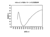
かかる要件(R1)について、再び図1に示す第1実施形態を参照して説明すると、発光素子120の透明電極111から出射した波長λ1の光と波長λ2の光は、発光素子の層内の干渉のしかたの違いなどに基づき、配光特性に違いが生じる。図12は、そのような配光特性に違いが生じた一例を示すグラフである。図12に示す例では、λ1=465nmの第1の発光ピーク及びλ2=550nmの第2の発光ピークについて、出光面の法線方向と測定方向がなす角即ち極角を−90°〜0°〜+90°と変化させて強度を測定し、0°方向を1とした相対値で測定結果を示している。
In the light source device of the present invention, the difference between the light distribution characteristic at the wavelength λ1 and the light distribution characteristic at the wavelength λ2 of the light emitted from the diffraction element is the light distribution characteristic at the wavelength λ1 and the light distribution characteristic at the wavelength λ2. (Hereinafter, this requirement is referred to as “requirement (R1)”).
The requirement (R1) will be described again with reference to the first embodiment shown in FIG. 1. The light having the wavelength λ1 and the light having the wavelength λ2 emitted from the
この例では、発光素子120から出光する光のうち第1の発光ピークに属する波長465nmの光は正面方向の光の強度に対する斜め方向の光の強度が比較的強く、第2の発光ピークに属する波長550nmの光は正面方向の光の強度に対する斜め方向の光の強度が比較的弱く、従って配光特性に差が存在している。このような配光特性を有する発光素子からの光を、さらに回折素子に透過させた後に、この配光特性の差が少なくなれば、要件(R1)を充足することになる。
In this example, light having a wavelength of 465 nm belonging to the first emission peak among the light emitted from the
図13は、図12の配光特性を有する光を回折素子に透過させた際に、回折素子からの出光する光の配光特性の一例を示すグラフである。図13では、図12より、465nmにおける配光特性と550nmにおける配光特性の差が縮まり、従って要件(R1)を充足している。 FIG. 13 is a graph showing an example of the light distribution characteristic of the light emitted from the diffraction element when the light having the light distribution characteristic of FIG. 12 is transmitted through the diffraction element. In FIG. 13, from FIG. 12, the difference between the light distribution characteristic at 465 nm and the light distribution characteristic at 550 nm is reduced, and therefore the requirement (R1) is satisfied.
かかる配光特性の差の減少は、極角0°以外の少なくともいずれかの極角及び傾斜方向において観察されれば要件(R1)を充足するものとすることができるが、極角60°方向において観察した際に要件(R1)を充足することが好ましい。即ち、前記発光素子から出光する光の波長λ1(nm)の正面方向の強度を1とした際の極角60°方向の相対強度RA1、前記発光素子から出光する光の波長λ2(nm)の正面方向の強度を1とした際の極角60°方向の相対強度RA2、前記回折素子から出光する光の波長λ1(nm)の正面方向の強度を1とした際の極角60°方向の相対強度RB1、及び前記回折素子から出光する光の波長λ2(nm)の正面方向の強度を1とした際の極角60°方向の相対強度RB2が、式(1):
|RA1−RA2|>|RB1−RB2| ・・・式(1)
の関係を満たす(以下、当該要件を「要件(R2)」という。)ことが特に好ましい。当該要件(R2)を充足することにより、観察角度による色味の変化が少なくなるため、液晶表示装置のバックライトや照明装置などの光源として有用である。
Such a decrease in the difference in light distribution characteristics can satisfy the requirement (R1) if observed in at least one polar angle other than the polar angle of 0 ° and the inclination direction. It is preferable to satisfy the requirement (R1) when observed in. That is, the relative intensity RA1 in the polar angle direction of 60 ° when the intensity in the front direction of the wavelength λ1 (nm) of the light emitted from the light emitting element is 1, and the wavelength λ2 (nm) of the light emitted from the light emitting element. The relative intensity RA2 in the
| RA1-RA2 |> | RB1-RB2 | Formula (1)
(Hereinafter, the requirement is referred to as “requirement (R2)”). Satisfying the requirement (R2) reduces the change in color depending on the viewing angle, and is thus useful as a light source for a backlight of a liquid crystal display device, an illumination device, or the like.
図4は、図1に示される回折素子1をより詳細に示す斜視図である。図4に示す通り、回折素子1は、回折素子の基板20の一方の面に、断面矩形の畝状の凸部2を多数並列に配列した凹凸形状を有する凹凸構造体22を有し、それにより、面上において凸部2の延長方向に垂直な方向に、凹凸が繰り返す構造となっている。かかる凹凸形状により、回折素子1は回折格子として機能する。図5は、回折素子1を、その凸部2の延長方向に垂直な断面で切断した断面図である。回折格子の凹凸形状のピッチは、図5において矢印P1で示される長さとなる。かかるピッチを適宜調整することにより、上記要件(R1)、及び好ましくは上記要件(R2)を充足する回折素子を得ることができる。凹凸形状のピッチは、300〜4000nmであることが、かかる要件を充足し好ましい本発明の効果を得る上で好ましい。
FIG. 4 is a perspective view showing the
上に述べたλ1=465nmの第1の発光ピーク及びλ2=550nmの第2の発光ピークを有し、第1のピークのほうが広い配光特性を有する発光素子と組み合わせ、要件(R1)、要件(R2)を充足する回折素子を得ることについて、図15を参照して説明する。図15は、図4及び図5に示す回折素子1であってピッチが1600nmのものについて、正面方向の透過率を測定したグラフである。図15に示すように、465nmにおける正面透過率より550nmにおける正面透過率のほうが低い回折素子は、465nmより550nmにおいて、より多くの光を正面方向とは異なる角度に散乱させる。従って、このような回折素子を用いることにより、要件(R1)、要件(R2)を充足する光源装置を得ることができる。
In combination with the light emitting element having the first emission peak of λ1 = 465 nm and the second emission peak of λ2 = 550 nm described above, and the first peak has a wider light distribution characteristic, the requirement (R1), the requirement Obtaining a diffraction element satisfying (R2) will be described with reference to FIG. FIG. 15 is a graph obtained by measuring the transmittance in the front direction for the
回折素子の材質は、光学部材として機能しうる任意の材質、例えば入射した光の一部を反射又は透過させる材質とすることができる。具体的には、透明樹脂等の有機材料とすることが、光透過性能と加工の容易さの観点から好ましい。 The material of the diffraction element can be any material that can function as an optical member, for example, a material that reflects or transmits part of incident light. Specifically, an organic material such as a transparent resin is preferable from the viewpoint of light transmission performance and ease of processing.
かかる透明樹脂は、凹凸形状を容易に形成できるという観点から、硬化性樹脂を硬化させたものが好ましい。硬化性樹脂としては、熱硬化性のものと、エネルギー線硬化性のものが挙げられる。エネルギー線は、可視光線、紫外線、電子線、X線を含む。 Such a transparent resin is preferably one obtained by curing a curable resin from the viewpoint that an uneven shape can be easily formed. Examples of the curable resin include thermosetting resins and energy beam curable resins. Energy rays include visible light, ultraviolet rays, electron beams, and X-rays.
熱硬化性樹脂の具体例としては、フェノール樹脂、尿素樹脂、ジアリルフタレート樹脂、メラミン樹脂、グアナミン樹脂、不飽和ポリエステル樹脂、ポリウレタン樹脂、エポキシ樹脂、アミノアルキッド樹脂、メラミン−尿素共縮合樹脂、珪素樹脂、及びポリシロキサン樹脂が挙げられる。 Specific examples of the thermosetting resin include phenol resin, urea resin, diallyl phthalate resin, melamine resin, guanamine resin, unsaturated polyester resin, polyurethane resin, epoxy resin, aminoalkyd resin, melamine-urea cocondensation resin, silicon resin. And polysiloxane resins.
エネルギー線硬化性樹脂としては、ラジカル重合性不飽和基及び/又はカチオン重合性基を有する低分子量化合物、又は樹脂等が挙げられる。なお、ラジカル重合性不飽和基及び/又はカチオン重合性基は、1分子中に2以上含んでいてもよい。 Examples of the energy ray curable resin include a low molecular weight compound having a radically polymerizable unsaturated group and / or a cationically polymerizable group, or a resin. In addition, the radically polymerizable unsaturated group and / or the cation polymerizable group may contain two or more in one molecule.
前記ラジカル重合性不飽和基を有する低分子量化合物としては、エチレン、プロピレン等のα−オレフィン;ブタジエン、イソプレン等の共役ジエン化合物;スチレン、α−メチルスチレン、t−ブチルスチレン、ジビニルベンゼン、ビニルナフタレン、4−ビニルピリジン等のラジカル反応性芳香族化合物;アクリル酸、メタクリル酸、フマール酸、マレイン酸、エンド−ビシクロ[2.2.1]−5−ヘプテン−2,8−ジカルボン酸(エンディック酸)、テトラヒドロフタル酸、イタコン酸、シトラコン酸、クロトン酸、イソクロトン酸等の不飽和カルボン酸;アクリル酸クロライド、メタクリル酸クロライド、マレイン酸クロライド等の不飽和カルボン酸のハライド;アクリルアミド、メタクリルアミド、マレイミド等の不飽和カルボン酸のアミド若しくはイミド誘導体;無水マレイン酸、無水エンディック酸、無水シトラコン酸等の不飽和カルボン酸の無水物;マレイン酸モノメチル、マレイン酸ジメチル、メチル(メタ)アクリレート、エチル(メタ)アクリレート、2−ヒドロキシエチル(メタ)アクリレート、2−ヒドロキシプロピル(メタ)アクリレート、ジメチルアミノエチル(メタ)アクリレート、2−エチルヘキシル(メタ)アクリレート、シクロヘキシル(メタ)アクリレート、イソボルニル(メタ)アクリレート、ジシクロペンテニル(メタ)アクリレート、アリル(メタ)アクリレート、フェニル(メタ)アクリレート、ベンジル(メタ)アクリレート、フエノキシエチル(メタ)アクリレート、へキサンジオールジ(メタ)アクリレート、ネオペンチルグリコールジ(メタ)アクリレート、ジエチレングリコールジ(メタ)アクリレート、トリシクロデカンジメチロールジ(メタ)アクリレート、トリメチロールプロパントリ(メタ)アクリレート、プロピオン酸・ジペンタエリスリトールトリ(メタ)アクリレート、プロピオン酸・ジペンタエリスリトールテトラ(メタ)アクリレート、ジペンタエリスリトールへキサ(メタ)アクリレート等の不飽和カルボン酸のエステル誘導体;ビニルトリクロロシラン、ビニルトリメトキシシラン、ビニルトリエトキシシラン、p−スチリルトリメトキシシラン、3−(メタ)アクリロキシプロピルトリメトキシシラン、3−(メタ)アクリロキシトリエトキシシラン等のラジカル反応不飽和基を有するシラン化合物;等が挙げられる。 Examples of the low molecular weight compound having a radical polymerizable unsaturated group include α-olefins such as ethylene and propylene; conjugated diene compounds such as butadiene and isoprene; styrene, α-methylstyrene, t-butylstyrene, divinylbenzene, and vinylnaphthalene. Radical-reactive aromatic compounds such as 4-vinylpyridine; acrylic acid, methacrylic acid, fumaric acid, maleic acid, endo-bicyclo [2.2.1] -5-heptene-2,8-dicarboxylic acid (endic Acid), tetrahydrophthalic acid, itaconic acid, citraconic acid, crotonic acid, isocrotonic acid and other unsaturated carboxylic acids; acrylic acid chloride, methacrylic acid chloride, maleic acid chloride and other unsaturated carboxylic acid halides; acrylamide, methacrylamide, Unsaturated carbo such as maleimide Amide or imide derivatives of acids; anhydrides of unsaturated carboxylic acids such as maleic anhydride, endic anhydride, citraconic anhydride; monomethyl maleate, dimethyl maleate, methyl (meth) acrylate, ethyl (meth) acrylate, 2-hydroxyethyl (meth) acrylate, 2-hydroxypropyl (meth) acrylate, dimethylaminoethyl (meth) acrylate, 2-ethylhexyl (meth) acrylate, cyclohexyl (meth) acrylate, isobornyl (meth) acrylate, dicyclopentenyl ( (Meth) acrylate, allyl (meth) acrylate, phenyl (meth) acrylate, benzyl (meth) acrylate, phenoxyethyl (meth) acrylate, hexanediol di (meth) acrylate, neopen Diglycol di (meth) acrylate, diethylene glycol di (meth) acrylate, tricyclodecane dimethylol di (meth) acrylate, trimethylolpropane tri (meth) acrylate, propionic acid / dipentaerythritol tri (meth) acrylate, propionic acid / Ester derivatives of unsaturated carboxylic acids such as dipentaerythritol tetra (meth) acrylate and dipentaerythritol hexa (meth) acrylate; vinyltrichlorosilane, vinyltrimethoxysilane, vinyltriethoxysilane, p-styryltrimethoxysilane, 3 Silane compounds having a radical reaction unsaturated group such as-(meth) acryloxypropyltrimethoxysilane, 3- (meth) acryloxytriethoxysilane; and the like.
前記カチオン重合性基を有する低分子量化合物としては、ジシクロペンタジエンジオキサイド、(3,4−エポキシシクロヘキシル)メチル−3,4−エポキシシクロヘキサンカルボキシレート、ビス(2,3−エポキシシクロペンチル)エーテル、ビス(3,4−エポキシシクロヘキシルメチル)アジペート、ビス(3,4−エポキシ−6−メチルシクロヘキシルメチル)アジペート、(3,4−エポキシ−6−メチルシクロヘキシル)メチル−3,4−エポキシ−6−メチルシクロヘキサンカルボキシレート、ビス(3,4−エポキシシクロヘキシルメチル)アセタール、エチレングリコールのビス(3,4−エポキシシクロヘキシル)エーテル、エチレングリコールの3,4−エポキシシクロヘキサンカルボン酸ジエステル等の脂環式エポキシ基を含有する化合物;エチレングリコールジグリシジルエーテル、プロピレングリコールジグリシジルエーテル、ポリエチレングリコールジグリシジルエーテル、ポリプロピレングリコールジグリシジルエーテル、1,4−ブタンジオールジグリシジルエーテル、ネオペンチルグリコールジグリシジルエーテル、1,6−ヘキサンジオールジグリシジルエーテル、グリセリンジグリシジルエーテル、ジグリセリンテトラグリシジルエーテル、トリメチロールプロパントリグリシジルエーテル、スピログリコールジグリシジルエーテル等のグリシジル基を含有するエポキシ化合物;3−エチル−3−メトキシメチルオキセタン、3−エチル−3−エトキシメチルオキセタン、3−エチル−3−ブトキシメチルオキセタン、3−エチル−3−アリルオキシメチルオキセタン、3−メチル−3−ヒドロキシメチルオキセタン、3−エチル−3−ヒドロキシメチルオキセタン、3−エチル−3−(2’−ヒドロキシエチル)オキシメチルオキセタン、3−エチル−3−(2’−ヒドロキシ−3’−フェノキシプロピル)オキシメチルオキセタン、3−エチル−3−(2’−ヒドロキシ−3’−ブトキシプロピル)オキシメチルオキセタン、3−エチル−3−[2’−(2”−エトキシエチル)オキシメチル]オキセタン等のオキセタン環を含有する化合物;等が挙げられる。 Examples of the low molecular weight compound having a cationic polymerizable group include dicyclopentadiene dioxide, (3,4-epoxycyclohexyl) methyl-3,4-epoxycyclohexanecarboxylate, bis (2,3-epoxycyclopentyl) ether, bis (3,4-epoxycyclohexylmethyl) adipate, bis (3,4-epoxy-6-methylcyclohexylmethyl) adipate, (3,4-epoxy-6-methylcyclohexyl) methyl-3,4-epoxy-6-methyl Cyclohexane carboxylate, bis (3,4-epoxycyclohexylmethyl) acetal, bis (3,4-epoxycyclohexyl) ether of ethylene glycol, 3,4-epoxycyclohexanecarboxylic acid diester of ethylene glycol, etc. Compounds containing a poxy group; ethylene glycol diglycidyl ether, propylene glycol diglycidyl ether, polyethylene glycol diglycidyl ether, polypropylene glycol diglycidyl ether, 1,4-butanediol diglycidyl ether, neopentyl glycol diglycidyl ether, 1, Epoxy compounds containing a glycidyl group such as 6-hexanediol diglycidyl ether, glycerin diglycidyl ether, diglycerin tetraglycidyl ether, trimethylolpropane triglycidyl ether, spiroglycol diglycidyl ether; 3-ethyl-3-methoxymethyloxetane 3-ethyl-3-ethoxymethyloxetane, 3-ethyl-3-butoxymethyloxetane, 3-ethyl- -Allyloxymethyloxetane, 3-methyl-3-hydroxymethyloxetane, 3-ethyl-3-hydroxymethyloxetane, 3-ethyl-3- (2'-hydroxyethyl) oxymethyloxetane, 3-ethyl-3- ( 2'-hydroxy-3'-phenoxypropyl) oxymethyloxetane, 3-ethyl-3- (2'-hydroxy-3'-butoxypropyl) oxymethyloxetane, 3-ethyl-3- [2 '-(2 " -Ethoxyethyl) oxymethyl] a compound containing an oxetane ring such as oxetane;
前記ラジカル重合性不飽和基又はカチオン重合性基を有する樹脂としては、低分子量のポリエステル樹脂、ポリエーテル樹脂、アクリル樹脂、メタクリル樹脂、エポキシ樹脂、ウレタン樹脂、アルキッド樹脂、スピロアセタール樹脂、ポリブタジエン樹脂、ポリチオールポリエン樹脂等の側鎖にラジカル重合性不飽和基又はカチオン重合性基を有する樹脂が挙げられる。 Examples of the resin having a radical polymerizable unsaturated group or a cationic polymerizable group include low molecular weight polyester resins, polyether resins, acrylic resins, methacrylic resins, epoxy resins, urethane resins, alkyd resins, spiroacetal resins, polybutadiene resins, Examples thereof include resins having a radically polymerizable unsaturated group or a cationically polymerizable group in the side chain such as a polythiol polyene resin.
エネルギー線として紫外線や可視光線を用いる場合には、硬化性樹脂の中に光重合開始剤、光増感剤などを含ませることができる。光重合開始剤としては、アセトフェノン類、ベンゾフェノン類、ミヒラーベンゾイルベンゾエート、α−アミロキシムエステル、テトラメチルチウラムモノサルファイド、チオキサントン類等が挙げられる。光増感剤としてn−ブチルアミン、トリエチルアミン、トリ−n−ブチルホスフィン等が挙げられる。 When ultraviolet rays or visible rays are used as energy rays, a photopolymerization initiator, a photosensitizer, or the like can be included in the curable resin. Examples of the photopolymerization initiator include acetophenones, benzophenones, Michler benzoylbenzoate, α-amyloxime ester, tetramethylthiuram monosulfide, thioxanthones, and the like. Examples of the photosensitizer include n-butylamine, triethylamine, and tri-n-butylphosphine.
回折素子を構成する透明樹脂は、加工性の観点からガラス転移温度が60〜300℃であることが好ましく、100〜250℃であることがより好ましい。なお、ガラス転移温度は示差走査熱量分析(DSC)により測定することができる。 The transparent resin constituting the diffraction element preferably has a glass transition temperature of 60 to 300 ° C, more preferably 100 to 250 ° C from the viewpoint of processability. The glass transition temperature can be measured by differential scanning calorimetry (DSC).
前記透明樹脂は、顔料や染料のごとき着色剤、蛍光増白剤、分散剤、熱安定剤、光安定剤、紫外線吸収剤、帯電防止剤、酸化防止剤、滑剤、溶剤などの配合剤が適宜配合されたものであってもよい。 The transparent resin may be appropriately mixed with coloring agents such as pigments and dyes, fluorescent brighteners, dispersants, heat stabilizers, light stabilizers, UV absorbers, antistatic agents, antioxidants, lubricants, solvents, and the like. It may be blended.
回折素子は、前記透明樹脂からなる1層のみからなってもよく、前記透明樹脂の層と、前記透明樹脂または他の樹脂からなる他の層との積層体であってもよい。例えば、透明なフィルムと、前記各種の透明樹脂の層との積層体とし、以下に述べる方法により透明樹脂の層の表面に凹凸形状を設けたものとすることができる。透明なフィルムとしては、透明であれば特に限定されないが、例えば、脂環式構造を有する樹脂等を挙げることができる。 The diffraction element may consist of only one layer made of the transparent resin, or may be a laminate of the transparent resin layer and another layer made of the transparent resin or another resin. For example, a laminate of a transparent film and the above-described various transparent resin layers can be used, and a concavo-convex shape can be provided on the surface of the transparent resin layer by the method described below. The transparent film is not particularly limited as long as it is transparent, and examples thereof include a resin having an alicyclic structure.
回折素子は、前記透明樹脂を公知の方法で成形することによって得ることができる。成形法としては、キャスト成形法、押出成形法、インフレーション成形法などが挙げられる。 The diffraction element can be obtained by molding the transparent resin by a known method. Examples of the molding method include a cast molding method, an extrusion molding method, and an inflation molding method.
上記のような畝を有する回折素子は、リソグラフィー法と現像エッチング法との組み合わせによって、または転写型または転写ロールを用いた転写法によって、得ることができる。具体的には、エネルギー線硬化性樹脂を流延して塗膜を得、該塗膜に畝に対応するパターンでエネルギー線を照射して、該パターンを現像することによって畝を有する回折素子を得ることができる。 The diffraction element having the above-described defects can be obtained by a combination of a lithography method and a development etching method, or a transfer method using a transfer mold or a transfer roll. Specifically, a diffraction element having wrinkles is obtained by casting an energy ray curable resin to obtain a coating film, irradiating the coating film with energy rays in a pattern corresponding to wrinkles, and developing the pattern. Can be obtained.
また特に、上で述べた、透明なフィルムの上に凹凸形状を有する透明樹脂層を製造する場合、液体状の透明樹脂をフィルム上に流延して透明樹脂の塗膜を得、該塗膜に畝に対応した凹凸を有する金型またはロールを押し当て、該押し当てている状態でエネルギー線を照射し、エネルギー線硬化性樹脂を硬化させることによって畝を有する透明樹脂層を得ることができる。このような製造方法によれば、凹凸形状の形成を比較的短時間で行なうことができ、その結果、インラインでの効率的な生産が可能となり、長尺の光学部材を低コストで得ることができるため、特に好ましい。 In particular, when producing a transparent resin layer having an uneven shape on a transparent film as described above, a liquid transparent resin is cast on the film to obtain a transparent resin coating film. A transparent resin layer having wrinkles can be obtained by pressing a mold or roll having irregularities corresponding to wrinkles to the surface, irradiating energy rays in the pressed state, and curing the energy ray curable resin. . According to such a manufacturing method, it is possible to form the concavo-convex shape in a relatively short time, and as a result, efficient in-line production is possible, and a long optical member can be obtained at low cost. This is particularly preferable because it can be performed.
(第2実施形態)
本発明の光源装置において、回折格子は、上記第1の実施形態が有するものに限られず、種々の形態をとることができる。例えば、第1の実施形態において回折素子は面上の一方向のみに繰り返し単位を有する凹凸形状を有していたが、これに限られず、以下に説明する第2実施形態のように、複数方向に繰り返し単位を有する凹凸形状を有していてもよい。
図2は、本発明の第2の実施形態に係る光源装置を概略的に示す断面図である。本実施形態は、第1実施形態における回折素子1に変えて回折素子6を有する点において、第1実施形態と異なっている。図6は図2における回折素子6をより詳細に示す斜視図である。本実施形態において、回折素子6は、図6に示すように、回折格子の基板60と、その一方の面に設けられた、直方体状の凸部7が正方格子状に整列してなる回折構造体72を有することにより、面上の直交する2方向に繰り返し単位を有する凹凸形状を有している。図7は、図6に示す回折素子をより詳細に示す上面図である。図7に示す通り、回折素子6は、直方体状の凸部7が回折素子の面上の2方向に、P4及びP6で示される寸法を有し、P3及びP5で示されるピッチで繰り返す凹凸形状を有している。このような構造を有することにより、面上の複数の方向において、色味の変化を抑制することができる。
(Second Embodiment)
In the light source device of the present invention, the diffraction grating is not limited to that of the first embodiment, and can take various forms. For example, in the first embodiment, the diffractive element has a concavo-convex shape having a repeating unit only in one direction on the surface. However, the present invention is not limited to this, and a plurality of directions as in the second embodiment described below. May have a concavo-convex shape having repeating units.
FIG. 2 is a cross-sectional view schematically showing a light source device according to the second embodiment of the present invention. The present embodiment is different from the first embodiment in that a
第2の実施形態における回折素子のピッチも、第1の実施形態と同様、良好な効果を有するよう適宜決定することができる。図16は、図6及び図7に示す回折素子6において、直方体の寸法(直方体の高さ、並びに図7における2方向の幅P4及びP6)及びピッチ(P3及びP5)を変化させた場合における正面透過率を測定したグラフである。図16において、実線は、直方体の高さ幅P4及びP6をいずれも0.51μmとしピッチP3及びP5をいずれも2.05μmとした場合、破線は、直方体の高さ幅P4及びP6をいずれも1.28μmとしピッチP3及びP5をいずれも2.55μmとした場合における測定結果を示す。このようにピッチを変化させた場合における正面方向の透過率を元に、本発明の要件を満たしうるピッチを選択することができる。
Similarly to the first embodiment, the pitch of the diffraction elements in the second embodiment can also be determined as appropriate so as to have a good effect. FIG. 16 shows a case where the dimensions of the rectangular parallelepiped (the height of the rectangular parallelepiped and the widths P4 and P6 in two directions in FIG. 7) and the pitch (P3 and P5) are changed in the
(第3実施形態)
上記第1及び第2の実施形態の光源装置においては、回折素子は、光が出射する平坦な面上に回折格子が設けられた態様であるが、本発明はこれに限られず、回折素子は、以下に説明する第3実施形態のように、平坦でない面上に回折格子が設けられた態様であってもよい。
(Third embodiment)
In the light source devices of the first and second embodiments, the diffraction element is a mode in which a diffraction grating is provided on a flat surface from which light is emitted. However, the present invention is not limited to this, and the diffraction element is As in the third embodiment described below, the diffraction grating may be provided on a non-flat surface.
図3は、本発明の第3の実施形態に係る光源装置を概略的に示す断面図である。本実施形態は、第1実施形態における回折素子1に変えて回折素子11を有する点において、第1実施形態と異なっている。図8は図3における回折素子11をより詳細に示す斜視図である。本実施形態において、回折素子11は、底面部81と、その上に設けられた断面三角形の畝状の凸部12を有する構造を、回折素子の基板として有しており、この畝の表面上に、回折効果を発現する回折格子が形成されている。
FIG. 3 is a cross-sectional view schematically showing a light source device according to the third embodiment of the present invention. This embodiment is different from the first embodiment in that a
図9は、図8に示す回折素子11を、その凸部12の延長方向に垂直な断面で切断した断面図である。図9に示す通り、凸部12の傾斜面上に微小な凸部13(図3及び図8において不図示)が設けられており、かかる微小な凸部13により構成される凹凸形状が回折構造体を形成し、回折格子としての機能を発現する。この回折素子において、第1の凹凸形状である微小な凸部13による凹凸形状のピッチは、図9において矢印P1で示される長さである。一方、かかる微小な凸部13をその表面に有する、第2の凹凸形状である凸部12による凹凸形状のピッチは、P1より長い矢印P7で示される長さである。凸部12による凹凸形状(第2の凹凸形状)のピッチは、前記第1の凹凸形状よりも大きければよいが、例えば10〜1000μmとすることができる。この態様においては、ピッチP1を300〜4000nmとすることが、前記要件(1)及び好ましくは(2)を充足し本発明の効果を得る上で好ましい。ここで、微小な凸部13の形状は、例えば凸部12と平行に延長する畝状の形状とすることができ、また、凸部12の斜面上において、凸部12の延長方向と平行な方向及びその方向と垂直な方向の2方向に繰り返し単位を構成する直方体状の形状とすることもできる。本実施形態のように第1の凹凸形状と第2の凹凸形状とを組み合わせた構造の回折素子を設けることにより、第2の凹凸形状による光学的効果を得ながら、且つ観察角度による色味の変化をさらに低減することができる。
FIG. 9 is a cross-sectional view of the
(第4実施形態)
本発明の第4の実施形態は、第3実施形態における回折素子11において、第1の凹凸形状である微小な凸部による凹凸形状を設ける位置を変更した点において第1実施形態と異なる。図10は、本発明の第4の実施形態に係る光源装置における回折素子11をその凸部12の延長方向に垂直な断面で切断した断面図である。本実施形態において、回折素子11は、第3の実施形態と同様の断面三角形の畝状の凸部12を有しているが、その傾斜面15には微小な凹凸形状を有さず、凸部12の頂部に設けられた平坦な部分上に微小な凸部14が設けられている。かかる微小な凸部14により構成される凹凸形状が、回折格子としての機能を発現する。
(Fourth embodiment)
The fourth embodiment of the present invention is different from the first embodiment in that, in the
この回折素子において、第1の凹凸形状である微小な凸部14による凹凸形状のピッチは、図10において矢印P1で示される長さである。一方、かかる微小な凸部14をその頂部に有する、第2の凹凸形状である凸部12による凹凸形状のピッチは、P1より長い矢印P8で示される長さである。凸部12による凹凸形状(第2の凹凸形状)のピッチは、前記第1の凹凸形状よりも大きければよいが、例えば10〜1000μmとすることができる。この態様においては、ピッチP1を300〜4000nmとすることが、前記要件(1)及び好ましくは(2)を充足し本発明の効果を得る上で好ましい。ここで、微小な凸部14の形状は、例えば凸部12と平行に延長する畝状の形状とすることができ、また、凸部12の斜面上において、凸部12の延長方向と平行な方向及びその方向と垂直な方向の2方向に繰り返し単位を構成する直方体状の形状とすることもできる。
In this diffractive element, the pitch of the concavo-convex shape by the minute
本実施形態のように第1の凹凸形状と第2の凹凸形状とを組み合わせた構造の回折素子を設けることにより、第2の凹凸形状による光学的効果を得ながら、且つ観察角度による色味の変化をさらに低減することができる。具体的には、図8に示すプリズム状の形状を有する凸部12による第2の凹凸形状を有するが、その表面に微小な凸部による第1の凹凸形状を有しない形状の構造体を発光素子上に設けた場合、凸部12のプリズムによる効果、例えば図11の矢印A1で示される経路のように光が進むことによる拡散の効果を得ることができるが、プリズムの頂部においては、成形が不完全となり、そのため矢印A2のように光が進み、結果として構造体の一部において所望の効果が得られないこととなる。ここで、図10に示すような微細な凸部14による凹凸構造をプリズムの頂部に設けることにより、頂部を透過する光について拡散等の効果を与え、且つ、観察角度による色味の変化の低減の効果をも与えることができる。
By providing a diffractive element having a structure in which the first concavo-convex shape and the second concavo-convex shape are combined as in the present embodiment, the optical effect of the second concavo-convex shape is obtained, and the color depending on the observation angle is obtained. The change can be further reduced. Specifically, a light emitting structure having a second concavo-convex shape by the
(拡散層)
本発明の光源装置は、任意に、拡散層を有することができる。より具体的には、上記各種の実施形態において、回折素子1、6、11と基板101との間に、拡散剤を含有する拡散層を設けてもよく、また、回折素子を構成する材料として拡散剤を含有するものを用い、回折素子が拡散層としての機能を有するものとしてもよい。かかる拡散層を有することにより、光の経路を拡散させ、それにより観察角度による色味の変化をさらに低減することができる。一般に、回折素子を有さず拡散層のみを有する光源装置において、観察角度による色味の変化が低減できるほど拡散層の拡散力を高めようとすると、輝度の低下、光源装置の厚さや重量の増加などの不所望な効果が発現するが、本発明の光源装置においては、回折素子と拡散層とを組み合わせることにより、そのような不所望な効果の発現なしに、観察角度による色味の変化をより良好に改善することができる。
(Diffusion layer)
The light source device of the present invention can optionally have a diffusion layer. More specifically, in the various embodiments described above, a diffusion layer containing a diffusing agent may be provided between the
拡散層を構成する拡散剤としては、無機、および有機のフィラーを適宜選択して用いることができる。無機フィラーとしては、ガラス、酸化ケイ素、水酸化アルミニウム、酸化アルミニウム、酸化チタン、酸化亜鉛、硫酸バリウム、マグネシウムシリケート等からなるもの;有機フィラーとしては、フッ素樹脂、ポリスチレン樹脂、アクリル樹脂、ポリカーボネート樹脂、シリコーン樹脂、ポリエチレン樹脂、エチレン−酢酸ビニル共重合体、アクリロニトリル、ポリウレタン、ポリ塩化ビニル、ポリアクリロニトリル、ポリアミド、ポリシロキサン樹脂、メラミン樹脂、ベンゾグアナミン樹脂、またはこれらの架橋物等からなるものが挙げられる。フィラーの形状としては、特に限定されず、球状、楕円体状、立方体状、針状、棒状、紡錘形状、板状、鱗片状、繊維状などが挙げられるが、中でも光の拡散方向を等方的にできる点で球状、もしくは球状に近い楕円体状が好ましい。フィラーの大きさは、好ましくは直径0.2μm〜50μm、より好ましくは0.5μm〜10μmである。尚、ここでいう直径は、完全な球状ではない場合は、同一体積の球の直径で代用される。針状のような一方向に著しく寸法の異なるフィラーの場合は、その方向に垂直な断面の断面積と同一面積の円の直径で代用する。フィラーの屈折率は、バインダー樹脂の屈折率と異なることが好ましく、屈折率差が0.05以上であることがより好ましい。フィラーは、単独の素材、大きさ、屈折率等の性質ものを用いてもよく、また、2種類以上のフィラーを混合して用いても良い。また、フィラーとして2種類以上の素材からなるものを用いてもよい。上記フィラーと、バインダーとして上記透明樹脂を含有する拡散層におけるフィラーの含有量は、バインダー100重量部に対して、好ましくは0.1〜20重量部、より好ましくは1〜10重量部である。 As a diffusing agent constituting the diffusion layer, inorganic and organic fillers can be appropriately selected and used. Inorganic fillers include glass, silicon oxide, aluminum hydroxide, aluminum oxide, titanium oxide, zinc oxide, barium sulfate, magnesium silicate, etc .; organic fillers include fluororesin, polystyrene resin, acrylic resin, polycarbonate resin, Examples thereof include silicone resin, polyethylene resin, ethylene-vinyl acetate copolymer, acrylonitrile, polyurethane, polyvinyl chloride, polyacrylonitrile, polyamide, polysiloxane resin, melamine resin, benzoguanamine resin, or a cross-linked product thereof. The shape of the filler is not particularly limited, and examples thereof include a spherical shape, an ellipsoidal shape, a cubic shape, a needle shape, a rod shape, a spindle shape, a plate shape, a scale shape, and a fiber shape. Spherical or nearly ellipsoidal shape is preferable in that it can be achieved. The size of the filler is preferably 0.2 μm to 50 μm in diameter, more preferably 0.5 μm to 10 μm. In addition, when the diameter here is not a perfect sphere, the diameter of the sphere of the same volume is substituted. In the case of a filler having a significantly different size in one direction such as a needle shape, a diameter of a circle having the same area as the cross-sectional area of the cross section perpendicular to the direction is substituted. The refractive index of the filler is preferably different from the refractive index of the binder resin, and the refractive index difference is more preferably 0.05 or more. The filler may be a single material, size, refractive index or other properties, or a mixture of two or more fillers. Moreover, you may use what consists of 2 or more types of raw materials as a filler. The filler and the filler content in the diffusion layer containing the transparent resin as a binder are preferably 0.1 to 20 parts by weight, more preferably 1 to 10 parts by weight with respect to 100 parts by weight of the binder.
(用途、液晶表示装置)
本発明の光源装置の用途は、特に限定されないが、観察角度による色味が少ない利点を生かした、液晶表示装置のバックライト、照明装置などの光源とすることができる。
本発明の液晶表示装置は、前記本発明の光源装置を備える。具体的には、直下型バックライト装置として本発明の光源装置を備え、加えて各種の表示モードの液晶セルを有し、バックライト装置からの出射光を、液晶セルを通して表示面から出射させる態様とすることができる。本発明の液晶表示装置は、例えばツイステッドネマチック(TN)モード、スーパーツイステッドネマチック(STN)モード、ハイブリッドアラインメントネマチック(HAN)モード、バーティカルアラインメント(VA)モード、マルチドメインバーティカルアラインメント(MVA)モード、インプレーンスイッチング(IPS)モード、オプティカリーコンペンセイテッドバイリフジエンス(OCB)モードなどの表示モードによるものとすることができる。
(Applications, liquid crystal display devices)
Although the use of the light source device of the present invention is not particularly limited, it can be used as a light source for a backlight of a liquid crystal display device, an illumination device, and the like, taking advantage of less color depending on the viewing angle.
The liquid crystal display device of the present invention includes the light source device of the present invention. Specifically, the light source device of the present invention is provided as a direct type backlight device, in addition to the liquid crystal cell of various display modes, and the light emitted from the backlight device is emitted from the display surface through the liquid crystal cell. It can be. The liquid crystal display device of the present invention includes, for example, a twisted nematic (TN) mode, a super twisted nematic (STN) mode, a hybrid alignment nematic (HAN) mode, a vertical alignment (VA) mode, a multi-domain vertical alignment (MVA) mode, an in-plane It can be based on display modes such as switching (IPS) mode, optically compensated birefringence (OCB) mode.
(その他の任意の構成要素)
本発明の光源装置及び本発明の液晶表示装置は、前記実施形態に限定されず、本願特許請求の範囲内及びその均等の範囲内での変更を施すことができる。また、他の任意の構成要素をさらに含むことができる。
例えば、任意の構成要素として、前記発光素子を封止する封止部材、前記発光素子に電流を共有するための配線、発光素子及び回折素子を保持するための筐体、枠部材等を必要に応じて有することができる。
また、本発明の光源装置において、回折素子は、回折素子1のように1方向に繰返し単位を有するもの、回折素子6のように2方向に繰返し単位を有するものに限られず、3方向以上に繰り返し単位を有するもの、例えば6角形の凸部が連続した凹凸形状とすることにより3方向に繰返し単位を有するものとすることもできる。そのような3方向以上に繰り返し単位を有する構造は、また、第2の凹凸形状12の斜面上の微細な凹凸形状としても設けることができる。
(Other optional components)
The light source device of the present invention and the liquid crystal display device of the present invention are not limited to the above-described embodiments, and can be modified within the scope of the claims of the present application and the equivalent scope thereof. Moreover, other arbitrary components can be further included.
For example, as an optional component, a sealing member that seals the light emitting element, wiring for sharing current with the light emitting element, a housing for holding the light emitting element and the diffraction element, a frame member, and the like are required. Can have depending on.
In the light source device of the present invention, the diffraction element is not limited to one having a repeating unit in one direction like the
以下、実施例に基づき、本発明についてさらに詳細に説明する。なお、本発明は下記実施例に限定されるものではない。 Hereinafter, the present invention will be described in more detail based on examples. In addition, this invention is not limited to the following Example.
<製造例1:拡散層−回折素子層積層体の調製>
ウレタンアクリレート系のUV硬化性樹脂(屈折率1.53)に、直径2μmのシリコーン粒子(商品名「トスパール120」、GE東芝シリコーン社製、屈折率1.43)を、組成物全量中10重量%となるよう添加し、攪拌機を用いてよく混合し、樹脂−粒子組成物を得た。
透明フィルム(商品名「ゼオノアフィルム」、日本ゼオン株式会社製)の上に、前記樹脂-粒子組成物を50μm塗布し紫外線を照射し硬化させ、透明フィルム−拡散樹脂層からなる積層体P1を得た。
積層体P1の拡散樹脂層側の面上に、UV硬化性樹脂(商品名「PAK−01」、東洋合成工業製)を厚さ10μmで塗付し、透明フィルム−拡散樹脂層−UV硬化性樹脂層(未硬化)からなる積層体P2を得た。
積層体P2のUV硬化性樹脂層に、所定の凹凸構造を有する面を有する金属製モールドを押し付けた。その後、積層体P2の透明フィルム側の面から、紫外線照射し、UV硬化性樹脂層を硬化させ、所定の凹凸構造が転写された回折素子層とした。その後金属製モールドを剥離し、透明フィルム−拡散樹脂層−回折素子層の層構成を有する積層体P3を得た。得られた積層体P3の回折素子層側の面上には、図4及び図5に概略的に図示される、高さH1が800nm、凸部幅P2が800nm、ピッチP1が1600nmの凹凸形状が形成されていた。
<Production Example 1: Preparation of diffusion layer-diffractive element layer laminate>
10 wt% of urethane acrylate UV curable resin (refractive index: 1.53) and silicone particles having a diameter of 2 μm (trade name “
On a transparent film (trade name “ZEONOR FILM”, manufactured by Nippon Zeon Co., Ltd.), 50 μm of the resin-particle composition is applied and cured by irradiating with ultraviolet rays to obtain a laminate P1 composed of a transparent film-diffusing resin layer. It was.
A UV curable resin (trade name “PAK-01”, manufactured by Toyo Gosei Co., Ltd.) is applied in a thickness of 10 μm on the surface of the laminate P1 on the side of the diffusion resin layer, and transparent film-diffusion resin layer-UV curable A laminate P2 made of a resin layer (uncured) was obtained.
A metal mold having a surface having a predetermined concavo-convex structure was pressed against the UV curable resin layer of the laminate P2. Thereafter, the laminate P2 was irradiated with ultraviolet rays from the surface on the transparent film side to cure the UV curable resin layer, thereby obtaining a diffractive element layer to which a predetermined concavo-convex structure was transferred. Thereafter, the metal mold was peeled off to obtain a laminate P3 having a layer structure of transparent film-diffusion resin layer-diffraction element layer. On the surface of the obtained laminate P3 on the side of the diffraction element layer, an uneven shape having a height H1 of 800 nm, a protrusion width P2 of 800 nm, and a pitch P1 of 1600 nm, schematically shown in FIGS. Was formed.
<製造例2:回折素子積層体の調製>
シリコーン粒子を添加しなかった他は製造例1と同様に操作し、透明フィルム−樹脂層−回折素子層の層構成を有する積層体P4を得た。
得られた積層体の透明フィルム側の面を入光面、回折素子層側の面を出光面として、様々な波長の光における正面透過率を、分光光度計(型番「V−570」、日本分光社製)を用いて測定した。結果を図15に示す。
図15に示す結果から明らかな通り、波長465nmにおける正面透過率に比べて波長550nmにおける正面透過率が低く、従ってこの回折素子は、λ1=465nmの第1の発光ピーク及びλ2=550nmの第2の発光ピークを有し、第1の発光ピークのほうが広い配光特性を有する発光素子と組み合わせて、本発明の光源装置を構成しうることが分かった。
<Production Example 2: Preparation of diffraction element laminate>
Except not having added the silicone particle, it operated like the manufacture example 1, and obtained the laminated body P4 which has the layer structure of a transparent film-resin layer-diffraction element layer.
With the surface of the obtained laminate on the transparent film side as the light incident surface and the surface on the diffraction element layer side as the light exit surface, the front transmittance of light of various wavelengths was measured with a spectrophotometer (model number “V-570”, Japan (Manufactured by Spectroscopic Co., Ltd.). The results are shown in FIG.
As is clear from the results shown in FIG. 15, the front transmittance at a wavelength of 550 nm is lower than the front transmittance at a wavelength of 465 nm. Therefore, the diffractive element has a first emission peak at λ1 = 465 nm and a second emission peak at λ2 = 550 nm. It has been found that the light source device of the present invention can be configured in combination with a light emitting element having a light distribution characteristic of the first light emission peak and having a wider light distribution characteristic.
<実施例1及び比較例1>
図1に概略的に示される構成を有する有機EL光源装置を製造した。
<Example 1 and Comparative Example 1>
An organic EL light source device having a configuration schematically shown in FIG. 1 was produced.
(1−1:発光素子の調製)
厚さ1.1mmのガラス製の基板101の一方の面101A上に、透明電極111、有機発光層121及び反射電極112を含む有機EL発光素子120を設けた。
(1-1: Preparation of light-emitting element)
An organic EL
この段階で、有機EL発光素子に電流を通電し、基板101の他方の面101Bから出光する波長465nmの青色光及び波長550nmの緑色光についての配光特性を測定した(比較例1)。測定は、面101Bの正面(法線方向)に、分光放射輝度計(BM−7 トプコン)を配置し、輝度の測定方向と発光面法線方向とがなす角が−90〜90°となるよう発光面を動かし、それぞれの角度における放射強度及び発光スペクトルを測定し、波長465nm及び550nmにおける配光特性を求めた。測定結果を図12に示す。
At this stage, a current was passed through the organic EL light emitting element, and the light distribution characteristics of blue light having a wavelength of 465 nm and green light having a wavelength of 550 nm emitted from the other surface 101B of the
(1−2:有機EL光源装置の製造)
さらに、基板101の面101B上に、回折素子1として、製造例2で得た積層体P4を、透明フィルムが基板101に面するように配置し、図1に示す構成を有する有機EL光源装置100を製造した。得られた有機EL発光素子100に電流を通電し、出光面109から出光する波長465nmの青色光及び波長550nmの緑色光についての配光特性を(1−1)と同様に測定した(実施例1)。輝度を測定する角度を傾ける方向は、回折素子の畝の延長方向に垂直な方向とした。測定結果を図13に示す。
(1-2: Manufacture of organic EL light source device)
Furthermore, on the surface 101B of the
図12及び図13の結果の対比から明らかな通り、発光素子に加えて回折素子を備える本発明の光源装置は、回折素子を設けていない発光素子に比べて、青色光と緑色光の配光特性の差が小さく、観察角度による色味の変化が少ないことが分かる。 As apparent from the comparison of the results of FIGS. 12 and 13, the light source device of the present invention having the diffraction element in addition to the light emitting element distributes blue light and green light as compared with the light emitting element not provided with the diffraction element. It can be seen that the difference in characteristics is small and the change in color depending on the observation angle is small.
<実施例2>
製造例2で得た積層体P4に代えて、製造例1で得た積層体P3を用いた他は実施例1と同様に操作し、有機EL光源装置を製造し、配光特性を測定した。結果を図14に示す。
図14の結果から明らかな通り、回折素子に加えて拡散層を備える実施例2の光源装置は、青色光と緑色光の配光特性の差がさらに小さく、観察角度による色味の変化がさらに少ないことが分かる。
<Example 2>
It replaced with the laminated body P4 obtained by manufacture example 2, and operated similarly to Example 1 except having used laminated body P3 obtained by manufacture example 1, manufactured the organic electroluminescent light source device, and measured the light distribution characteristic. . The results are shown in FIG.
As is clear from the results of FIG. 14, the light source device of Example 2 provided with the diffusion layer in addition to the diffraction element has a smaller difference in light distribution characteristics between blue light and green light, and further changes in color depending on the observation angle. I understand that there are few.
1、6、11 回折素子
2、7 凸部
20、60 回折素子の基板
22、72 回折構造体
100 光源装置
101 基板
109 出光面
111 透明電極
112 反射電極
120 発光素子
1, 6, 11
Claims (3)
前記回折素子は、ピッチが300〜4000nmである第1の凹凸形状を有し、
前記発光素子から出光する光の波長λ1(nm)の正面方向の強度を1とした際の極角60°方向の相対強度RA1、
前記発光素子から出光する光の波長λ2(nm)の正面方向の強度を1とした際の極角60°方向の相対強度RA2、
前記回折素子から出光する光の波長λ1(nm)の正面方向の強度を1とした際の極角60°方向の相対強度RB1、及び
前記回折素子から出光する光の波長λ2(nm)の正面方向の強度を1とした際の極角60°方向の相対強度RB2が、式(1):
|RA1−RA2|>|RB1−RB2| ・・・式(1)
の関係を満たす光源装置。 A light emitting element having a first emission peak having a peak wavelength of λ1 and a second emission peak having a peak wavelength of λ2, a diffraction element provided on the light emitting side of the light emitting element, and a light emitting side of the light emitting element And a diffusion layer provided in
The diffraction element has a first uneven shape with a pitch of 300 to 4000 nm,
Relative intensity RA1 in the polar angle direction of 60 ° when the intensity in the front direction of the wavelength λ1 (nm) of the light emitted from the light emitting element is 1.
The relative intensity RA2 in the polar angle 60 ° direction when the intensity in the front direction of the wavelength λ2 (nm) of the light emitted from the light emitting element is 1.
Relative intensity RB1 in the polar angle direction of 60 ° when the intensity in the front direction of the wavelength λ1 (nm) of the light emitted from the diffractive element is 1, and the front of the wavelength λ2 (nm) of the light emitted from the diffractive element The relative intensity RB2 in the direction of the polar angle of 60 ° when the direction intensity is set to 1 is the formula (1):
| RA1-RA2 |> | RB1-RB2 | Formula (1)
Light source device that satisfies the relationship.
前記回折素子は、前記第1の凹凸形状より大きいピッチを有する第2の凹凸形状をさらに有し、
前記第1の凹凸形状は、前記第2の凹凸形状を構成する面上に設けられている光源装置。 The light source device according to claim 1,
The diffractive element further has a second concavo-convex shape having a pitch larger than the first concavo-convex shape,
The first uneven shape is a light source device provided on a surface constituting the second uneven shape.
Priority Applications (1)
| Application Number | Priority Date | Filing Date | Title |
|---|---|---|---|
| JP2008273592A JP5633105B2 (en) | 2008-10-23 | 2008-10-23 | Light source device and liquid crystal display device |
Applications Claiming Priority (1)
| Application Number | Priority Date | Filing Date | Title |
|---|---|---|---|
| JP2008273592A JP5633105B2 (en) | 2008-10-23 | 2008-10-23 | Light source device and liquid crystal display device |
Publications (2)
| Publication Number | Publication Date |
|---|---|
| JP2010102965A JP2010102965A (en) | 2010-05-06 |
| JP5633105B2 true JP5633105B2 (en) | 2014-12-03 |
Family
ID=42293446
Family Applications (1)
| Application Number | Title | Priority Date | Filing Date |
|---|---|---|---|
| JP2008273592A Expired - Fee Related JP5633105B2 (en) | 2008-10-23 | 2008-10-23 | Light source device and liquid crystal display device |
Country Status (1)
| Country | Link |
|---|---|
| JP (1) | JP5633105B2 (en) |
Families Citing this family (10)
| Publication number | Priority date | Publication date | Assignee | Title |
|---|---|---|---|---|
| JP6062636B2 (en) * | 2011-03-10 | 2017-01-18 | ローム株式会社 | Organic EL device |
| JP5803506B2 (en) * | 2011-09-28 | 2015-11-04 | 日本ゼオン株式会社 | Light emitting device and lighting apparatus |
| JP5942528B2 (en) * | 2012-03-27 | 2016-06-29 | 大日本印刷株式会社 | Light diffusing film, polarizing plate, image forming apparatus and display device |
| KR101421026B1 (en) * | 2012-06-12 | 2014-07-22 | 코닝정밀소재 주식회사 | Light extraction layer substrate for oled and method of fabricating thereof |
| JPWO2014013990A1 (en) * | 2012-07-17 | 2016-06-30 | 三菱化学株式会社 | Lighting device |
| WO2014057647A1 (en) * | 2012-10-11 | 2014-04-17 | パナソニック株式会社 | Organic electroluminescence element and lighting device |
| JP5560359B2 (en) * | 2013-03-01 | 2014-07-23 | 株式会社日立製作所 | Organic light emitting diode and light source device using the same |
| KR101859303B1 (en) * | 2013-06-12 | 2018-06-28 | 미쯔비시 케미컬 주식회사 | Light-extraction film for el, method for manufacturing light-extraction film for el, and planar light-emitting body |
| US9799853B2 (en) * | 2013-08-12 | 2017-10-24 | 3M Innovative Properties Company | Emissive article with light extraction film |
| CN103490020A (en) * | 2013-09-30 | 2014-01-01 | 京东方科技集团股份有限公司 | Organic electroluminescence device, manufacturing method thereof, display device and illuminating device |
Family Cites Families (3)
| Publication number | Priority date | Publication date | Assignee | Title |
|---|---|---|---|---|
| JP4388305B2 (en) * | 2003-05-16 | 2009-12-24 | 富士フイルム株式会社 | Spectral anisotropic scattering film, polarizing plate, and liquid crystal display device |
| JP4410123B2 (en) * | 2005-02-10 | 2010-02-03 | 株式会社東芝 | Organic EL display |
| JP2006269163A (en) * | 2005-03-23 | 2006-10-05 | Konica Minolta Holdings Inc | Organic electroluminescent element |
-
2008
- 2008-10-23 JP JP2008273592A patent/JP5633105B2/en not_active Expired - Fee Related
Also Published As
| Publication number | Publication date |
|---|---|
| JP2010102965A (en) | 2010-05-06 |
Similar Documents
| Publication | Publication Date | Title |
|---|---|---|
| JP5633105B2 (en) | Light source device and liquid crystal display device | |
| TWI828698B (en) | Color conversion element and display device including the same | |
| US7852435B2 (en) | Light-condensing film, liquid-crystal panel and backlight as well as manufacturing process for light-condensing film | |
| CN100544056C (en) | Light-emitting element, light-emitting display device, and lighting device | |
| CN102742352B (en) | Organic electroluminescent element, lighting device, and method for forming light output layer | |
| US8179034B2 (en) | Light extraction film for organic light emitting diode display and lighting devices | |
| US20040217702A1 (en) | Light extraction designs for organic light emitting diodes | |
| US20090015142A1 (en) | Light extraction film for organic light emitting diode display devices | |
| KR102099781B1 (en) | Optical film for reducing color shift and organic light emitting display employing the same | |
| KR102063202B1 (en) | Polarizing plate and liquid crystal display apparatus comprising the same | |
| KR101640719B1 (en) | Module for liquid crystal display apparatus and liquid crystal display apparatus comprising the same | |
| WO2015022882A1 (en) | Optical film, barrier film, light conversion member, backlight unit and liquid crystal display device | |
| JP6367001B2 (en) | Display device and liquid crystal display device | |
| KR102120808B1 (en) | Optical film for reducing color shift and organic light emitting display employing the same | |
| WO2015041316A1 (en) | Liquid crystal display device and light conversion member | |
| JP2010177133A (en) | Polarized light-emitting element | |
| US9927565B2 (en) | Light guide plate and display device having the same | |
| JP2007035550A (en) | Substrates for electroluminescence elements | |
| CN110646980B (en) | Liquid crystal display | |
| KR20180028798A (en) | Glass light guide plate, backlight unit and display device including the same | |
| KR20180070183A (en) | Heat-dissipative shielding sheet and preparation method thereof | |
| CN1524195A (en) | Substrate equipped with cholesteric layer and display device equipped with the substrate | |
| TWI612347B (en) | Optical sheet and optical display comprising the same | |
| US20180143469A1 (en) | Quantum dot film and backlight module | |
| JP7756819B1 (en) | display device |
Legal Events
| Date | Code | Title | Description |
|---|---|---|---|
| A621 | Written request for application examination |
Free format text: JAPANESE INTERMEDIATE CODE: A621 Effective date: 20110912 |
|
| A977 | Report on retrieval |
Free format text: JAPANESE INTERMEDIATE CODE: A971007 Effective date: 20121207 |
|
| A131 | Notification of reasons for refusal |
Free format text: JAPANESE INTERMEDIATE CODE: A131 Effective date: 20130115 |
|
| A521 | Request for written amendment filed |
Free format text: JAPANESE INTERMEDIATE CODE: A523 Effective date: 20130312 |
|
| A131 | Notification of reasons for refusal |
Free format text: JAPANESE INTERMEDIATE CODE: A131 Effective date: 20130917 |
|
| A521 | Request for written amendment filed |
Free format text: JAPANESE INTERMEDIATE CODE: A523 Effective date: 20131025 |
|
| A131 | Notification of reasons for refusal |
Free format text: JAPANESE INTERMEDIATE CODE: A131 Effective date: 20140318 |
|
| A521 | Request for written amendment filed |
Free format text: JAPANESE INTERMEDIATE CODE: A523 Effective date: 20140513 |
|
| TRDD | Decision of grant or rejection written | ||
| A01 | Written decision to grant a patent or to grant a registration (utility model) |
Free format text: JAPANESE INTERMEDIATE CODE: A01 Effective date: 20140916 |
|
| A61 | First payment of annual fees (during grant procedure) |
Free format text: JAPANESE INTERMEDIATE CODE: A61 Effective date: 20140929 |
|
| R150 | Certificate of patent or registration of utility model |
Ref document number: 5633105 Country of ref document: JP Free format text: JAPANESE INTERMEDIATE CODE: R150 |
|
| R250 | Receipt of annual fees |
Free format text: JAPANESE INTERMEDIATE CODE: R250 |
|
| R250 | Receipt of annual fees |
Free format text: JAPANESE INTERMEDIATE CODE: R250 |
|
| R250 | Receipt of annual fees |
Free format text: JAPANESE INTERMEDIATE CODE: R250 |
|
| LAPS | Cancellation because of no payment of annual fees |