JP5593714B2 - Electronic element shield structure and electronic device equipped with the same - Google Patents
Electronic element shield structure and electronic device equipped with the same Download PDFInfo
- Publication number
- JP5593714B2 JP5593714B2 JP2010019361A JP2010019361A JP5593714B2 JP 5593714 B2 JP5593714 B2 JP 5593714B2 JP 2010019361 A JP2010019361 A JP 2010019361A JP 2010019361 A JP2010019361 A JP 2010019361A JP 5593714 B2 JP5593714 B2 JP 5593714B2
- Authority
- JP
- Japan
- Prior art keywords
- electronic device
- metal fitting
- shield structure
- electronic element
- view
- Prior art date
- Legal status (The legal status is an assumption and is not a legal conclusion. Google has not performed a legal analysis and makes no representation as to the accuracy of the status listed.)
- Expired - Fee Related
Links
Images


Classifications
-
- H—ELECTRICITY
- H05—ELECTRIC TECHNIQUES NOT OTHERWISE PROVIDED FOR
- H05K—PRINTED CIRCUITS; CASINGS OR CONSTRUCTIONAL DETAILS OF ELECTRIC APPARATUS; MANUFACTURE OF ASSEMBLAGES OF ELECTRICAL COMPONENTS
- H05K9/00—Screening of apparatus or components against electric or magnetic fields
-
- H—ELECTRICITY
- H05—ELECTRIC TECHNIQUES NOT OTHERWISE PROVIDED FOR
- H05K—PRINTED CIRCUITS; CASINGS OR CONSTRUCTIONAL DETAILS OF ELECTRIC APPARATUS; MANUFACTURE OF ASSEMBLAGES OF ELECTRICAL COMPONENTS
- H05K9/00—Screening of apparatus or components against electric or magnetic fields
- H05K9/0067—Devices for protecting against damage from electrostatic discharge
-
- G—PHYSICS
- G06—COMPUTING OR CALCULATING; COUNTING
- G06F—ELECTRIC DIGITAL DATA PROCESSING
- G06F1/00—Details not covered by groups G06F3/00 - G06F13/00 and G06F21/00
- G06F1/16—Constructional details or arrangements
- G06F1/18—Packaging or power distribution
- G06F1/181—Enclosures
-
- G—PHYSICS
- G06—COMPUTING OR CALCULATING; COUNTING
- G06F—ELECTRIC DIGITAL DATA PROCESSING
- G06F1/00—Details not covered by groups G06F3/00 - G06F13/00 and G06F21/00
- G06F1/16—Constructional details or arrangements
- G06F1/18—Packaging or power distribution
- G06F1/183—Internal mounting support structures, e.g. for supporting printed circuit boards
- G06F1/185—Mounting of expansion boards
- G06F1/186—Securing of expansion boards in correspondence to slots provided at the computer enclosure
-
- H—ELECTRICITY
- H05—ELECTRIC TECHNIQUES NOT OTHERWISE PROVIDED FOR
- H05K—PRINTED CIRCUITS; CASINGS OR CONSTRUCTIONAL DETAILS OF ELECTRIC APPARATUS; MANUFACTURE OF ASSEMBLAGES OF ELECTRICAL COMPONENTS
- H05K7/00—Constructional details common to different types of electric apparatus
- H05K7/02—Arrangements of circuit components or wiring on supporting structure
- H05K7/10—Plug-in assemblages of components, e.g. IC sockets
-
- H—ELECTRICITY
- H05—ELECTRIC TECHNIQUES NOT OTHERWISE PROVIDED FOR
- H05K—PRINTED CIRCUITS; CASINGS OR CONSTRUCTIONAL DETAILS OF ELECTRIC APPARATUS; MANUFACTURE OF ASSEMBLAGES OF ELECTRICAL COMPONENTS
- H05K9/00—Screening of apparatus or components against electric or magnetic fields
- H05K9/0007—Casings
- H05K9/0058—Casings specially adapted for optoelectronic applications
Landscapes
- Engineering & Computer Science (AREA)
- Theoretical Computer Science (AREA)
- Computer Hardware Design (AREA)
- General Engineering & Computer Science (AREA)
- Microelectronics & Electronic Packaging (AREA)
- Power Engineering (AREA)
- Human Computer Interaction (AREA)
- Physics & Mathematics (AREA)
- General Physics & Mathematics (AREA)
- Shielding Devices Or Components To Electric Or Magnetic Fields (AREA)
Description
本発明は、電子素子のシールド構造及びこれを備えた電子装置に関する。 The present invention relates to a shield structure for an electronic element and an electronic apparatus including the shield structure.
電子装置において、ノイズ対策は重要である。従来、電子装置におけるノイズ対策は種々提案されている。例えば、患者回路部と信号入出力部とを別々にシールドするシールド手段を設ける提案がされている(例えば、特許文献1)。また、例えば、第1の基板と第2の基板とを具備するデータ伝送装置において、第1の基板と第2の基板を覆い、電気的ノイズをシールドするシールド部材を設ける提案がされている(例えば、特許文献2)。 In electronic devices, noise countermeasures are important. Conventionally, various countermeasures for noise in electronic devices have been proposed. For example, a proposal has been made to provide shielding means for shielding the patient circuit section and the signal input / output section separately (for example, Patent Document 1). Further, for example, in a data transmission device including a first substrate and a second substrate, a proposal has been made to provide a shield member that covers the first substrate and the second substrate and shields electrical noise ( For example, Patent Document 2).
ところで、電子素子、特に、ノイズに敏感な電子素子を電子装置で用いる場合、これらの電子装置外部で発生した静電気が電子装置内の電子回路や電子素子に誤動作を生じさせることがある。例えば、光インターフェイスから電気インターフェイスへ変換する光電変換部を内包する光電変換素子は、ノイズが乗りやすく、ESD(Electrostatic discharge)耐性が低いという問題がある。 By the way, when an electronic device, particularly an electronic device sensitive to noise is used in an electronic device, static electricity generated outside the electronic device may cause malfunction in an electronic circuit or an electronic device in the electronic device. For example, a photoelectric conversion element including a photoelectric conversion unit that converts from an optical interface to an electrical interface has a problem that noise is easily applied and ESD (Electrostatic discharge) resistance is low.
これらの問題に対し、前記特許文献1、2の提案は、基板全体や特定の領域を対象としたシールドを行っており、電子素子のESD耐性向上の面で改良の余地があった。
With respect to these problems, the proposals in
そこで、本明細書開示の電子素子のシールド構造は、電子素子のESD耐性を向上することができる電子素子のシールド構造及び電子装置を提供することを課題とする。 Accordingly, an object of the shield structure for an electronic element disclosed in the present specification is to provide an electronic element shield structure and an electronic device that can improve ESD resistance of the electronic element.
本明細書開示の電子素子のシールド構造は、基板上に設けられた接地パターンと、導電性を有し、前記接地パターン上に搭載される電子素子を覆うとともに、前記接地パターンに接続される第1部材と、導電性を有し、前記電子素子を内部に備える電子装置の筐体と接触すると共に、前記接地パターン及び前記第1部材と接触する第2部材と、前記電子素子と外部機器とを接続するために前記電子素子と前記外部機器との接続部が露出する前記第2部材が備える開口から遠ざけて配置される離間部を備えた部材と、を、備え、前記第2部材は、前記筐体と接触する背面板と、前記接地パターンと接触する接地部と、前記第1部材と接触し、前記第1部材を前記基板側へ押圧する押圧金具を備え、前記第2部材と前記離間部を備えた部材との間に導電性を有する部材を配設している。 The shield structure for an electronic device disclosed in the present specification has a ground pattern provided on a substrate and a conductive material, covers the electronic device mounted on the ground pattern, and is connected to the ground pattern. A first member, a second member that is electrically conductive and contacts the housing of the electronic device including the electronic element therein; and the second member that contacts the ground pattern and the first member; the electronic element and an external device; A member provided with a separation portion disposed away from an opening provided in the second member through which a connection portion between the electronic element and the external device is exposed . A back plate that contacts the housing; a grounding portion that contacts the grounding pattern; and a pressing fitting that contacts the first member and presses the first member toward the substrate , and the second member and the Between a member with a separation part A member having conductivity are arranged.
電子素子は、接地パターンと第1部材とによって覆われる。これにより、電子素子は、ピン接続に加え、接地パターンへの面接続により信号接地SG(Signal Ground)が行われる。この結果、電子素子のESD耐性が向上する。また、第1部材は、第2部材を通じて筐体接地FG(Frame Ground)となる電子装置の筐体と同電位とされる。この結果、ノイズの影響を低減し、ESD耐性がさらに向上する。 The electronic element is covered with the ground pattern and the first member. Thereby, in addition to pin connection, the electronic element performs signal ground SG (Signal Ground) by surface connection to the ground pattern. As a result, the ESD resistance of the electronic element is improved. In addition, the first member is set to the same potential as the housing of the electronic device that becomes the housing ground FG (Frame Ground) through the second member. As a result, the influence of noise is reduced and ESD resistance is further improved.
本明細書開示の電子素子のシールド構造によれば、電子素子のESD耐性を向上することができる。 According to the shield structure for an electronic device disclosed in this specification, the ESD resistance of the electronic device can be improved.
以下、本発明の実施形態について、添付図面を参照しつつ説明する。ただし、図面中、各部の寸法、比率等は、実際のものと完全に一致するようには図示されていない場合がある。また、図面によっては細部が省略されている場合もある。 Hereinafter, embodiments of the present invention will be described with reference to the accompanying drawings. However, in the drawings, the dimensions, ratios, and the like of each part may not be shown so as to completely match the actual ones. Further, details may be omitted depending on the drawings.
≪第1形態≫
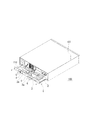
図1は、第1形態のシールド構造110を備えた電子装置100の斜視図である。また、図2は、第1形態のシールド構造110を備えた電子装置100の背面図である。図3は、電子装置100の使用例を示す説明図である。電子装置100は、サーバ150とプリンタやディスプレイ制御装置等の電気インターフェイスI/O(Input/Output)との間に配置され、光信号と電気信号との間の変換を行う。図3中、中間装置と記載されたものが電子装置100に相当する。図3に示す例では、サーバ150のCH00(CHANNEL00)と電子装置100のCV0(CONVERTER0)とが光ファイバケーブルで接続され、この間で光信号が送受信される。同様に、サーバ150のCH11(CHANNEL11)と電子装置100のCV1(CONVERTER1)とが光ファイバケーブルで接続され、この間で光信号が送受信される。また、CV0、CV1はケーブルを介してそれぞれ電気インターフェイス151へ接続され、それぞれ電気信号が送受信される。
≪First form≫
FIG. 1 is a perspective view of an
電子装置100は、筐体101の内部に、基板の一例であるプリント基板2を含む基板ユニット1を備えている。基板ユニット1には、背面板3が装着されている。基板ユニット1は、筐体101の背面側から筐体101内へ収納される。背面板3は、筐体101にネジ止めされる。背面板3は、EMI(Electro Magnetic Interference)を抑制する効果も有する。
The
プリント基板2には、電子回路が形成され、プリント基板2の後端部に電子素子4が配置されている。電子素子4は、光ファイバケーブルが接続される光電変換素子である。光ファイバケーブルが接続される電子素子4の接続部は、背面板3に設けられた開口3aから露出する。電子素子4の内部には、光インターフェイスから電気インターフェイスへ変換する光電変換回路が設けられたプリント基板が設けられている。このプリント基板における信号接地SGが電子素子4の外皮に接続されている。このように電子素子4は、光電変換部を内包している。シールド構造110は、この電子素子4におけるESD耐性を向上させるために施される。
An electronic circuit is formed on the printed
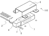
図4は、電子素子4の周辺を示す斜視図である。図5は、プリント基板2上に搭載された電子素子周辺の背面図である。
シールド構造110は、図4に示すようにプリント基板2上に設けられた接地パターン5を備える。電子素子4は、この接地パターン5上に搭載される。シールド構造110は、導電性を有する第1部材に相当する第1金具6を備えている。第1金具6は、図4、図5に示すように電子素子4を覆うとともに、接地パターン5に接続される。なお、図4において、第1金具6は、取り外された状態とされている。
FIG. 4 is a perspective view showing the periphery of the
The
図6は、プリント基板2の電子素子搭載面を示す説明図である。接地パターン5は、電子素子4の接地面の全域をカバーできるようにプリント基板2に設けられている。ただし、電子素子4が備える接地ピン4aや信号ピン4bに対応する位置には、これらのピンがプリント基板2に設けられたビアホールに挿入できるようにパターンは及んでいない。接地パターン5は、SGとなる。
FIG. 6 is an explanatory view showing an electronic element mounting surface of the printed
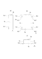
図7は、第1金具6の3面図である。図7(A)は平面図、図7(B)は側面図、図7(C)は背面図である。第1金具6は、天板6a、前面板6b、二枚の側板6cを備えている。すなわち、第1金具6は、四方に板体が配置されている。側板6cには、側方へ延びる鍔部6c1が設けられている。鍔部6c1には、ネジ穴6c2が設けられている。
FIG. 7 is a three-side view of the
このような第1金具6は、鍔部6c1が接地パターン5に接触するように電子素子4に覆い被される。このとき、第1金具6の内側には、第3部材に相当する導電性シート7が配置される。導電性シート7は、第1金具6を電子素子4上に覆い被せたときに電子素子4に当接するように図7に示すように天板6a、側板6cに貼付される。導電性シート7の貼付には導電性を有するアクリル系粘着剤を備えた接着テープを用いる。本実施例では、導電性シート7として日本ジッパーチュービング株式会社製のシールドフォーム(製品名)を用いた。
Such a
導電性シート7は、基材となるポリエステルクロスに銅層とニッケル層を設けたもので、表裏の導電性を有している。導電性シート7は、突起部7aを備えている。突起部7aは、シート内にポリウレタンフォームを配置することによって形成される。電子素子4と第1金具6とを密着させることができれば、導電性シート7の設置を廃止することもできるが、導電性シート7を配置することにより電子素子4と第1金具6との良好な接続状態を得ることができる。
The
第1金具6は、電子素子4に覆い被せ、鍔部6c1を接地パターン5に接触させる。そしてネジ穴6c2にネジ8を螺合することによって固定する。これにより、第1金具6と接地パターン5との導通が図られる。この結果、電子素子4は、全周亘って導電性素材に覆われる。また、電子素子4内のプリント基板のSGが電子素子4の外皮、導電性シート7、第1金具6を介して接地パターン5へ接続される。これにより、ESD耐量が向上する。そして、電子素子4における安定した光電変換、信号伝送が可能となる。なお、ネジ8に代えて半田を用いて第1金具6を接地パターン5に接続してもよい。また、接地パターン5と接続されたクリップ状の接続部を設け、この接続部に第1金具6を差し込むようにしてもよい。この場合、鍔部6c1を省略することができる。このように、第1金具6は、接地パターン5と電気的導通が取れるように取り付けられていればよい。
The first metal fitting 6 covers the
≪第2形態≫
つぎに、第2形態のシールド構造210について図8乃至図14を参照しつつ説明する。第2形態のシールド構造210は、第1形態のシールド構造110に、第2部材に相当する第2金具20が追加されている。なお、第1形態と共通する構成要素については、図面中、同一の参照番号を付し、その詳細な説明は省略する。
≪Second form≫
Next, the
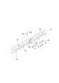
図8は、第2形態のシールド構造210を備えた電子装置200の斜視図であり、図9は、電子装置200の背面図である。図10は、第2形態における基板ユニット2を電子素子4上で切断した斜視図であり、図11は、第2形態における基板ユニット2を電子素子4上で切断した断面図である(図10中、A視)。図12は、シールド構造210に含まれる第2金具20の分解斜視図である。図13は、第2金具20に含まれる金具の3面図であり、図13(A)は背面図、図13(B)は側面図、図13(C)は底面図である。図14は、第2金具20に含まれる押圧金具24の3面図であり、図14(A)は平面図、図14(B)は背面図、図14(C)は側面図である。
FIG. 8 is a perspective view of the
第2金具20は、図12に詳細に示されているように、背面板21と接地部22と、接続部23、さらに、押圧金具24を備えている。背面板21は、図13に詳細に示されているように第1形態における背面板3に相当するもので、電子素子4と外部機器(例えば、図3に示すサーバ150)との接続部が露出する開口21aが設けられている。接地部22と接続部23は、金属板を屈曲成形して設けられており、背面板21に取り付けられている。接地部22は、基板2に設けられた接地パターン5に接地する部分である。また、接続部23は、図12に示すように第1金具6の外形に対応させた凹部23aを備え、第1金具6と接触する部分である。押圧金具24は、図14に詳細に示されているように、第1金具6の天板6aと平行となる押圧部24a、側板6cと平行となる二つのガイド部24bを備えている。押圧金具24は、図12に示すように接続部23に設けられた凹部23aにガイド部24bを挿入した状態で接続部23に取り付けられる。
As shown in detail in FIG. 12, the second metal fitting 20 includes a
このような第2金具20は、図10や図11に詳細に示されるように、接地部22が基板2上の接地パターン5に接触するように基板2上に搭載されて、ネジ止めされる。このとき、押圧金具24の押圧部24aと第1金具6との間、ガイド部24bと第1金具6との間に、導電性シート7と同様の導電性シート25を配置する。これにより、第2金具20と第1金具6との密着性が向上し、両者の電気的導通が良好なものとなる。なお、第2金具20の固定方法は、ネジ止めに限定されるものではない。
As shown in detail in FIGS. 10 and 11, the second metal fitting 20 is mounted on the
このような第2形態のシールド構造210は、図8に示すように、基板ユニット1が電子装置200内に設置されるときに、背面板21が図9に示すように筐体101に接触する。これにより、SGである第1金具6は、第2金具20を通じてFGと同電位とされる。この結果、ノイズの影響を低減し、ESD耐量がさらに向上する。そして、電子素子4における安定した光電変換、信号伝送が可能となる。なお、背面板21は、EMI(Electro Magnetic Interference)を抑制する効果も有する。
As shown in FIG. 8, the
≪第3形態≫
つぎに、第3形態のシールド構造310について図15乃至図22を参照しつつ説明する。第3形態のシールド構造310は、第2形態のシールド構造210に、第4部材に相当する第3金具30が追加されている。なお、第2形態と共通する構成要素については、図面中、同一の参照番号を付し、その詳細な説明は省略する。
≪Third form≫
Next, a
図15は、第3形態のシールド構造310を備えた電子装置300の斜視図である。図16(A)は、第3形態のシールド構造310を備えた電子装置300の後端部の平面図であり、図16(B)は、電子装置300の背面図である。図17は、第3形態における基板ユニット2を電子素子4上で切断した斜視図であり、図18は、第3形態における基板ユニット2を電子素子4上で切断した断面図である(図17中、A視)。図19は、第2金具20と第3金具30との分解斜視図である。図20は、第3金具30に含まれるカバー金具31の3面図であり、図20(A)は背面図、図20(B)は側面図、図20(C)は底面図である。図21は、第3金具30に含まれる受け金具32の3面図であり、図21(A)は平面図、図21(B)は側面図、図21(C)は底面図である。図22は、背面板21とカバー金具31の離間部との距離を示す説明図である。
FIG. 15 is a perspective view of an
第3金具30は、図17乃至図19に詳細に示されるように、カバー金具31と受け金具32とを備える。受け金具32は、背面板21に装着され、カバー金具31は、受け金具32に装着される。
As shown in detail in FIGS. 17 to 19, the third metal fitting 30 includes a
カバー金具31は、第2金具20に含まれる背面板21に設けられた開口21aから遠ざけて配置される離間部31aを備えている。このように離間部31aを設けるのは、背面板21の開口21aの周辺に接触したときのESD耐量が低いことに対応するためである。具体的には、電子素子4に光ファイバケーブルを接続した後、帯電した作業者が背面板21の開口21a周辺に接触すると放電が起きるおそれがある。そして、この放電に伴って発生したノイズが電子装置100内に入り込むことがある。ノイズは電子装置100を誤作動させるおそれがある。第2金具20に含まれる背面板21と離間部31aとは、図22に示すように、距離L離れている。図示するカバー金具31の例では、L=20mmに設定されている。このような離間部31aを設けることにより、電子装置300の外部で発生したノイズを電子素子4から遠ざけ、ESD耐量を向上させることができる。L=20mm以上となるように設定することができる。
The
離間部31aには、開口31a1が設けられており、この開口31a1を通じて電子素子4への光ファイバケーブルの接続が行われる。ただし、図18に示すように開口31aと電子素子4との距離が長い。換言すれば、電子素子4は、カバー金具31の奥側に位置する。このため、電子素子4への光ファイバケーブルの脱着作業が困難となる。そこで、カバー金具31は受け金具32に対し、脱着自在となっている。受け金具32は、背面板21への取付部32aを備えており、この取付部32aが背面板32へ固定される。受け金具32は、取付部32の上端部に溝32a1を備えている。この溝32a1には、カバー金具31が備える爪部31bが差し込まれる。カバー金具31は、爪部31bを溝32a1に差し込み、ネジ33を用いて受け金具32に固定される。
An opening 31a1 is provided in the
このような第3形態のシールド構造310は、図15に示すように、基板ユニット1が電子装置200内に設置されるときに、背面板21が図16(B)に示すように筐体101に接触する。これにより、SGである第1金具6は、第2金具20を通じてFGと同電位とされる。この結果、ノイズの影響を低減し、ESD耐量がさらに向上する。また、離間部31aを備えたことで、さらなるESD耐量の向上、特に、開口31a1周辺でのESD耐量を向上させることができる。この結果、電子素子4における安定した光電変換、信号伝送が可能となる。
As shown in FIG. 15, the
≪第4形態≫
つぎに、第4形態のシールド構造410について図23乃至図28を参照しつつ説明する。第4形態のシールド構造410は、第3形態のシールド構造310における第3金具30に代えて、第4金具40を備えている。この第4金具40は、第4部材に相当する。なお、第3形態と共通する構成要素については、図面中、同一の参照番号を付し、その詳細な説明は省略する。
≪Fourth form≫
Next, a
図23は、第4形態のシールド構造410を備えた電子装置400の斜視図である。図24(A)は、第4形態のシールド構造410を備えた電子装置400の後端部の平面図であり、図24(B)は、電子装置400の背面図である。図25は、第4金具40の斜視図である。図26は、第4金具40の3面図であり、図26(A)は背面図、図26(B)は側面図、図26(C)は底面図である。図27は、第4形態のシールド構造410の一部を側方から見た模式図である。図28は、第4形態のシールド構造における導電性シート41の配置を示す模式図である。
FIG. 23 is a perspective view of the
第4金具40は、図25、図26に示すように、中央部に設けられた当接部40aとその両側に延設された離間部40bを備えている。離間部40bには開口40b1が設けられている。
As shown in FIGS. 25 and 26, the fourth metal fitting 40 includes an
第4金具40は、当接部40aを背面板21に当接させて背面板21に取り付けられる。このとき、離間部40bと背面板21との間には、図27、図28に示すように導電性シート7と同様の導電性シート41が配置される。この導電性シート41が配置されることにより、第4形態の離間部40bと背面板21との距離は、第3形態の離間部31aと離間部21との距離Lよりも短く、2mmに設定されている。導電性シート41は、図28に示すように、開口40b1の周囲に配置されている。
The fourth metal fitting 40 is attached to the
このように導電性シート41を備えることにより、ノイズの装置内部に浸入することを防ぎESD耐量を向上させることができる。すなわち、導電性シート41を開口40b1の周囲に配置することにより、背面板21と離間部40bとの間を低インピーダンス化することができる。この結果、発生ノイズ電圧が低減され、電子装置400内の電子素子4、その他の電気回路、電子素子への影響を低減することができる。導電性シート41は、広い接触面積を確保することができるため、低抵抗にすることができる。
By providing the
このような離間部31a及び導電性シート41を備えた第4形態のシールド構造410は、ESD耐量の向上、特に、開口40b1周辺でのESD耐量を向上させることができる。この結果、電子素子4における安定した光電変換、信号伝送が可能となる。
The
≪効果確認≫
つぎに、上述した種々のシールド構造の効果確認試験について説明する。ここでは、FGが行われる第2形態〜第4形態のシールド構造について説明する。シールド構造の効果確認試験を行う際は、実際の使用状況に近い状況を創出するために、光ファイバケーブル50を電子素子4へ接続する。試験で用いた光ファイバケーブル50は、古河電気工業株式会社製である。図29は、電子装置に接続される光ファイバケーブル50の説明図であり、図29(A)はコネクタ部の平面図、図29(B)はコネクタ部の側面図、図29(C)は、ケーブルの断面図である。光ファイバケーブル50は、シリコン樹脂及びポリアミド樹脂による光ファイバ51とその周囲に設けられたアラミド繊維による緩衝層、さらに最外皮となるポリ塩化ビニルによる被覆を備えている。
≪Effect confirmation≫
Next, the effect confirmation test of the various shield structures described above will be described. Here, the shield structure of the 2nd form-the 4th form in which FG is performed is explained. When conducting the effect confirmation test of the shield structure, the
図30は、ESD試験機55の説明図である。ESD試験機55は、ニードル状の放電電極55aを備えている。効果確認試験は、この放電電極55aを測定箇所に接触させる接触放電による直接放電試験とした。印加回数は、1秒間隔で25回とした。
FIG. 30 is an explanatory diagram of the
(対策無し)
第1金具6、第2金具20等のシールド構造を備えておらず、何らのESD耐性向上対策を施していない場合である。
電子装置の筐体の各所における測定ESD耐量は、〜±2kV程度であった。
(No measures)
This is a case where the shield structure such as the
The measured ESD immunity at various locations of the electronic device casing was about ˜ ± 2 kV.
(第2形態)
第1金具6と、第2金具20によるシールド構造210を備えた場合である。この場合、背面板21の開口21a周辺以外での測定ESD耐量は、〜±10kV程度となり、ESD耐性の向上がみられた。
ただし、背面板21の開口21a周辺での測定ESD耐量は、〜±2kV程度であった。
(Second form)
This is a case where the
However, the measured ESD tolerance around the
(第3形態)
第2形態に第3金具30を追加したシールド構造310を備えた場合である。この場合、離間部31aに設けられた開口31a1の周辺における測定ESD耐量は、〜±10kV程度となり、開口周辺におけるESD耐性の向上がみられた。
(Third form)
This is a case where a
(第4形態)
第2形態に第4金具40と導電性シート41を追加したシールド構造410を備えた場合である。この場合、離間部40bに設けられた開口40b1の周辺における測定ESD耐量は、〜±8kV程度となり、開口周辺におけるESD耐性の向上がみられた。なお、導電性シート41を取り外した状態のときの開口40b1の周辺における測定ESD耐量は、〜±6kV程度となった。これより、導電性シート41もESD耐性向上に寄与しているものと考察される。また、第3形態との比較により、背面板21と離間部の距離が長いほど、ESD耐量が高いと考えられる。
(4th form)
This is a case where a
本明細書開示のシールド構造は、電子装置のインターフェース部を対象として、SGとFGを行うことにより、ESD耐性を向上させている。 The shield structure disclosed in the present specification improves the ESD resistance by performing SG and FG on the interface part of the electronic device.
以上本発明の好ましい実施例について詳述したが、本発明は係る特定の実施例に限定されるものではなく、特許請求の範囲に記載された本発明の要旨の範囲内において、種々の変形、変更が可能である。 Although the preferred embodiments of the present invention have been described in detail above, the present invention is not limited to the specific embodiments, and various modifications, within the scope of the gist of the present invention described in the claims, It can be changed.
(付記)
(付記1)
基板上に設けられた接地パターンと、
導電性を有し、前記接地パターン上に搭載される電子素子を覆うとともに、前記接地パターンに接続される第1部材と、
を、備えたことを特徴とする電子素子のシールド構造。
(Appendix)
(Appendix 1)
A ground pattern provided on the substrate;
A first member having electrical conductivity and covering an electronic element mounted on the ground pattern and connected to the ground pattern;
A shield structure for an electronic device, comprising:
(付記2)
基板上に設けられた接地パターンと、
導電性を有し、前記接地パターン上に搭載される電子素子を覆うとともに、前記接地パターンに接続される第1部材と、
導電性を有し、前記電子素子を内部に備える電子装置の筐体と接触すると共に、前記接地パターン及び前記シールド部材と接触する第2部材と、
を備えたことを特徴とする電子素子のシールド構造。
(Appendix 2)
A ground pattern provided on the substrate;
A first member having electrical conductivity and covering an electronic element mounted on the ground pattern and connected to the ground pattern;
A second member that is electrically conductive and contacts the housing of an electronic device that includes the electronic element therein, and that contacts the ground pattern and the shield member;
A shield structure for an electronic device, comprising:
(付記3)
導電性を有し、前記第1部材の内側に配置されて前記電子素子と当接する第3部材を備えたことを特徴とする付記1又は2記載の電子素子のシールド構造。
(Appendix 3)
The shield structure for an electronic device according to
(付記4)
前記電子素子と外部機器とを接続するために前記第2部材が備える開口から遠ざけて配置される離間部を備えた第4部材を備えたことを特徴とした付記1乃至3のいずれか一項の電子素子のシールド構造。
(Appendix 4)
(付記5)
前記第2部材と前記第4部材との間に導電性を有する第5部材を配設したことを特徴とする付記4記載の電子素子のシールド構造。
(Appendix 5)
The shield structure for an electronic element according to
(付記6)
前記電子素子は、光電変換素子であることを特徴とした付記1乃至5のいずれか一項記載の電子素子のシールド構造。
(Appendix 6)
The shield structure for an electronic device according to any one of
(付記7)
付記1乃至6のいずれか一項記載の電子素子のシールド構造を備え電子装置。
(Appendix 7)
An electronic device comprising the shield structure for an electronic element according to any one of
1…基板ユニット 2…プリント基板 3…背面板
3a…開口 4…電子素子 4a…接地ピン
5…接地パターン 6…第1金具 7…導電性シート
20…第2金具 21…背面板 21a…開口
22…接地部 23…接続部 23a…凹部
24…押圧金具 25…導電性シート 30…第3金具
31…カバー金具 31a…離間部 31a1…開口
40…第4金具 40b…離間部 40b1…開口
41…導電性シート 100、200、300、400…電子装置
110、210、310、410…シールド構造
101…筐体
DESCRIPTION OF
Claims (4)
導電性を有し、前記接地パターン上に搭載される電子素子を覆うとともに、前記接地パターンに接続される第1部材と、
導電性を有し、前記電子素子を内部に備える電子装置の筐体と接触すると共に、前記接地パターン及び前記第1部材と接触する第2部材と、
前記電子素子と外部機器とを接続するために前記電子素子と前記外部機器との接続部が露出する前記第2部材が備える開口から遠ざけて配置される離間部を備えた部材と、
を、備え、
前記第2部材は、前記筐体と接触する背面板と、前記接地パターンと接触する接地部と、前記第1部材と接触し、前記第1部材を前記基板側へ押圧する押圧金具を備え、
前記第2部材と前記離間部を備えた部材との間に導電性を有する部材を配設したことを特徴とする電子素子のシールド構造。 A ground pattern provided on the substrate;
A first member having electrical conductivity and covering an electronic element mounted on the ground pattern and connected to the ground pattern;
A second member that is electrically conductive and contacts a housing of an electronic device including the electronic element therein, and that contacts the ground pattern and the first member;
A member provided with a separation portion disposed away from an opening provided in the second member from which a connection portion between the electronic device and the external device is exposed in order to connect the electronic device and the external device;
With
The second member includes a back plate that contacts the housing, a grounding portion that contacts the ground pattern, and a pressing fitting that contacts the first member and presses the first member toward the substrate .
A shield structure for an electronic device, wherein a conductive member is disposed between the second member and the member having the separation portion .
Priority Applications (4)
| Application Number | Priority Date | Filing Date | Title |
|---|---|---|---|
| JP2010019361A JP5593714B2 (en) | 2010-01-29 | 2010-01-29 | Electronic element shield structure and electronic device equipped with the same |
| US13/005,718 US8797763B2 (en) | 2010-01-29 | 2011-01-13 | Shield structure for an electronic element and electronic device |
| EP11152031A EP2355644A3 (en) | 2010-01-29 | 2011-01-25 | Shield structure for an electronic element and electronic device |
| KR1020110008347A KR101191468B1 (en) | 2010-01-29 | 2011-01-27 | Shield structure for an electronic element and electronic device comprising the same |
Applications Claiming Priority (1)
| Application Number | Priority Date | Filing Date | Title |
|---|---|---|---|
| JP2010019361A JP5593714B2 (en) | 2010-01-29 | 2010-01-29 | Electronic element shield structure and electronic device equipped with the same |
Publications (2)
| Publication Number | Publication Date |
|---|---|
| JP2011159741A JP2011159741A (en) | 2011-08-18 |
| JP5593714B2 true JP5593714B2 (en) | 2014-09-24 |
Family
ID=44041562
Family Applications (1)
| Application Number | Title | Priority Date | Filing Date |
|---|---|---|---|
| JP2010019361A Expired - Fee Related JP5593714B2 (en) | 2010-01-29 | 2010-01-29 | Electronic element shield structure and electronic device equipped with the same |
Country Status (4)
| Country | Link |
|---|---|
| US (1) | US8797763B2 (en) |
| EP (1) | EP2355644A3 (en) |
| JP (1) | JP5593714B2 (en) |
| KR (1) | KR101191468B1 (en) |
Families Citing this family (6)
| Publication number | Priority date | Publication date | Assignee | Title |
|---|---|---|---|---|
| US8724343B2 (en) * | 2011-06-27 | 2014-05-13 | Crestron Electronics Inc. | Hi-definition multimedia interface shield with fingers |
| JP5068394B1 (en) * | 2011-11-30 | 2012-11-07 | 三菱電機株式会社 | Control system, control device, connection line and drive device |
| CN106664815B (en) | 2014-08-01 | 2019-04-12 | 华为技术有限公司 | Electromagnetic shielding material and method for packaging optical module |
| US11457524B2 (en) * | 2019-04-29 | 2022-09-27 | Nxp B.V. | Integrated filter for de-sense reduction |
| US11102894B2 (en) * | 2020-01-10 | 2021-08-24 | The Boeing Company | Saddle type electrical enclosure |
| JP2026028671A (en) * | 2024-08-07 | 2026-02-20 | Astemo株式会社 | Electronic control unit |
Family Cites Families (31)
| Publication number | Priority date | Publication date | Assignee | Title |
|---|---|---|---|---|
| JPH0796009B2 (en) | 1989-01-23 | 1995-10-18 | オリンパス光学工業株式会社 | Shield device for endoscopic imaging device |
| JPH0397997A (en) | 1989-09-08 | 1991-04-23 | Oji Paper Co Ltd | Manufacturing method of coated paper for gravure printing |
| JPH0397997U (en) * | 1990-01-25 | 1991-10-09 | ||
| JPH052482A (en) | 1991-06-24 | 1993-01-08 | Fujitsu Ltd | Data processing device |
| JPH06283234A (en) * | 1993-03-29 | 1994-10-07 | Nec Eng Ltd | Internally storing method of external interface connector and cover structure |
| JPH0796009A (en) | 1993-09-30 | 1995-04-11 | Suzuki Motor Corp | Electric tricycle |
| JP3516407B2 (en) | 1994-04-08 | 2004-04-05 | 株式会社東芝 | Data transmission apparatus and X-ray CT apparatus using the same |
| KR0169840B1 (en) * | 1995-11-14 | 1999-04-15 | 양승택 | Printed Circuit Board Guide Rail System with Anti-Static Function |
| US5696669A (en) | 1996-01-11 | 1997-12-09 | Molex Incorporated | Shielding system for PC cards |
| US5717577A (en) * | 1996-10-30 | 1998-02-10 | Ericsson, Inc. | Gasketed shield can for shielding emissions of electromagnetic energy |
| US5763900A (en) * | 1996-12-05 | 1998-06-09 | Taiwan Liton Electronic Co. Ltd. | Infrared transceiver package |
| US6049469A (en) * | 1997-08-20 | 2000-04-11 | Dell Usa, L.P. | Combination electromagnetic shield and heat spreader |
| JP2000340305A (en) * | 1999-05-25 | 2000-12-08 | Seiko Epson Corp | External interface connector grounding structure |
| US6320122B1 (en) * | 1999-10-12 | 2001-11-20 | Hewlett Packard Company | Electromagnetic interference gasket |
| CN1409942A (en) | 1999-10-12 | 2003-04-09 | 电子设备屏蔽公司 | EMI shielding apparatus |
| JP3315969B2 (en) * | 2000-05-09 | 2002-08-19 | 株式会社ソニー・コンピュータエンタテインメント | Electronics |
| NL1016549C2 (en) | 2000-10-06 | 2002-04-10 | Stork Screens Bv | Method for the production of a card protected against interference radiation with a printed circuit. |
| JP2003017193A (en) | 2001-07-04 | 2003-01-17 | Nec Tokin Iwate Ltd | Shield connector |
| US6443768B1 (en) * | 2001-09-14 | 2002-09-03 | Molex Incorporated | Small form factor connector cage |
| CN101820741A (en) * | 2001-12-14 | 2010-09-01 | 莱尔德技术公司 | EMI shielding including lossy dielectrics |
| WO2003077377A1 (en) | 2002-03-06 | 2003-09-18 | Tyco Electronics Corporation | Receptacle assembly having shielded interface with pluggable electronic module |
| US6744640B2 (en) * | 2002-04-10 | 2004-06-01 | Gore Enterprise Holdings, Inc. | Board-level EMI shield with enhanced thermal dissipation |
| WO2004077898A2 (en) * | 2003-02-26 | 2004-09-10 | Wavezero Inc. | Methods and devices for connecting and grounding an emi shield to a printed circuit board |
| CN1833341B (en) * | 2003-03-31 | 2010-06-16 | 莫莱克斯公司 | Shielded Cans with Improved EMI Shielding Gasket Construction |
| JP4299152B2 (en) * | 2004-01-08 | 2009-07-22 | 日本碍子株式会社 | Electromagnetic wave shielding case and manufacturing method thereof |
| JP2006090471A (en) | 2004-09-24 | 2006-04-06 | Fuji Heavy Ind Ltd | Orthogonal gear pair design device |
| WO2006090471A1 (en) * | 2005-02-25 | 2006-08-31 | Fujitsu Limited | Plug-in unit and communication device |
| JP4703454B2 (en) * | 2006-03-27 | 2011-06-15 | 富士通株式会社 | Cage mounting structure for optical modules |
| CN101094584A (en) | 2006-06-21 | 2007-12-26 | 华硕电脑股份有限公司 | Shielding Modules for Electronic Components |
| CN101600331B (en) * | 2008-06-04 | 2012-10-03 | 富士康(昆山)电脑接插件有限公司 | Shield |
| JP2010192759A (en) * | 2009-02-19 | 2010-09-02 | Sanyo Electric Co Ltd | Electromagnetic shield structure of electronic apparatus housing |
-
2010
- 2010-01-29 JP JP2010019361A patent/JP5593714B2/en not_active Expired - Fee Related
-
2011
- 2011-01-13 US US13/005,718 patent/US8797763B2/en not_active Expired - Fee Related
- 2011-01-25 EP EP11152031A patent/EP2355644A3/en not_active Withdrawn
- 2011-01-27 KR KR1020110008347A patent/KR101191468B1/en not_active Expired - Fee Related
Also Published As
| Publication number | Publication date |
|---|---|
| EP2355644A3 (en) | 2011-10-05 |
| JP2011159741A (en) | 2011-08-18 |
| US8797763B2 (en) | 2014-08-05 |
| US20110188227A1 (en) | 2011-08-04 |
| KR20110089080A (en) | 2011-08-04 |
| EP2355644A2 (en) | 2011-08-10 |
| KR101191468B1 (en) | 2012-10-15 |
Similar Documents
| Publication | Publication Date | Title |
|---|---|---|
| JP5593714B2 (en) | Electronic element shield structure and electronic device equipped with the same | |
| CN112514546B (en) | Electronic equipment containing shielding components | |
| EP3345791B1 (en) | Camera module for vehicle | |
| JP6434656B2 (en) | Electronic equipment | |
| US8969730B2 (en) | Printed circuit solder connections | |
| US7612299B2 (en) | Shield assembly with gaskets | |
| JP4266764B2 (en) | Method and apparatus for connecting a multicore coaxial cable to a printed circuit board in a small connector | |
| JP4762002B2 (en) | Electronics | |
| JP2011114077A (en) | Electronic device | |
| EP4096372A1 (en) | Electronic device comprising interposer | |
| US20200067218A1 (en) | Terminal assembly and electronic apparatus | |
| CN103777698A (en) | Grounding features of a portable computing device | |
| JP6453758B2 (en) | Electrical equipment | |
| JP5287492B2 (en) | Electronic equipment | |
| JP2008192800A (en) | Electronics | |
| WO2021020710A1 (en) | Electronic device including flexible printed circuit board | |
| JP2020031050A (en) | Cable device | |
| US8525046B2 (en) | Electronic apparatus | |
| JP2013190981A (en) | Design plate and touch panel input display device | |
| KR20210004774A (en) | Receptacle connector | |
| TW201706784A (en) | Touch pad and circuit board of the touch pad | |
| JP2011053330A (en) | Electronic apparatus | |
| JP2011199023A (en) | Substrate assembly and electronic equipment including the same | |
| EP4692860A1 (en) | Radiographic imaging device | |
| JP2015050654A (en) | Electronic apparatus |
Legal Events
| Date | Code | Title | Description |
|---|---|---|---|
| A621 | Written request for application examination |
Free format text: JAPANESE INTERMEDIATE CODE: A621 Effective date: 20121005 |
|
| A977 | Report on retrieval |
Free format text: JAPANESE INTERMEDIATE CODE: A971007 Effective date: 20130919 |
|
| A131 | Notification of reasons for refusal |
Free format text: JAPANESE INTERMEDIATE CODE: A131 Effective date: 20130924 |
|
| A131 | Notification of reasons for refusal |
Free format text: JAPANESE INTERMEDIATE CODE: A131 Effective date: 20140422 |
|
| A521 | Written amendment |
Free format text: JAPANESE INTERMEDIATE CODE: A523 Effective date: 20140616 |
|
| TRDD | Decision of grant or rejection written | ||
| A01 | Written decision to grant a patent or to grant a registration (utility model) |
Free format text: JAPANESE INTERMEDIATE CODE: A01 Effective date: 20140708 |
|
| A61 | First payment of annual fees (during grant procedure) |
Free format text: JAPANESE INTERMEDIATE CODE: A61 Effective date: 20140721 |
|
| R150 | Certificate of patent or registration of utility model |
Ref document number: 5593714 Country of ref document: JP Free format text: JAPANESE INTERMEDIATE CODE: R150 |
|
| LAPS | Cancellation because of no payment of annual fees |