JP5522824B2 - Switching element loss reduction circuit - Google Patents
Switching element loss reduction circuit Download PDFInfo
- Publication number
- JP5522824B2 JP5522824B2 JP2009064257A JP2009064257A JP5522824B2 JP 5522824 B2 JP5522824 B2 JP 5522824B2 JP 2009064257 A JP2009064257 A JP 2009064257A JP 2009064257 A JP2009064257 A JP 2009064257A JP 5522824 B2 JP5522824 B2 JP 5522824B2
- Authority
- JP
- Japan
- Prior art keywords
- mosfet
- drain
- current
- switching element
- reverse current
- Prior art date
- Legal status (The legal status is an assumption and is not a legal conclusion. Google has not performed a legal analysis and makes no representation as to the accuracy of the status listed.)
- Active
Links
Images

Landscapes
- Rectifiers (AREA)
- Dc-Dc Converters (AREA)
- Power Conversion In General (AREA)
- Inverter Devices (AREA)
Description
本発明は、スイッチング動作に伴う逆向き電流による損失を抑制するためのスイッチング素子の損失低減回路に関するもので、より具体的には、MOSFETの寄生ダイオードを流れる電流の抑制を行う構成の改良に関する。 The present invention relates to a switching element loss reduction circuit for suppressing a loss due to a reverse current accompanying a switching operation, and more specifically to an improvement in a configuration for suppressing a current flowing through a parasitic diode of a MOSFET.
よく知られるように、インバータやコンバータ等のスイッチング電源では、MOSFETをスイッチング素子に利用することが行われている。MOSFETは、電圧制御素子なので駆動電力が小さく、単一極性キャリアによる動作のためキャリア蓄積効果がなく高速スイッチングが行える等の特徴を有することから電力制御の用途に好まれている。 As is well known, MOSFETs are used as switching elements in switching power supplies such as inverters and converters. MOSFETs are preferred for power control applications because they are voltage control elements and have low drive power and the ability to perform high-speed switching without carrier accumulation effects due to operation with a single polarity carrier.
電力制御の用途では各種のスイッチング方式が知られているが、その一つに、MOSFETをハイサイドおよびローサイドに配置して交互にオン・オフ動作させるハーフブリッジ方式の構成がある。また、より高効率化するため、例えば特許文献1などに見られるように、トランスの1次側に誘導性素子L,容量性素子Cを備えて共振動作させるハーフブリッジ共振型の構成も採用が多い。
Various switching methods are known for use in power control. One of them is a half-bridge configuration in which MOSFETs are arranged on the high side and the low side to perform on / off operations alternately. In order to achieve higher efficiency, a half-bridge resonance type configuration in which an inductive element L and a capacitive element C are provided on the primary side of the transformer to perform resonance operation, as shown in
ハーフブリッジ方式など、ハイサイドおよびローサイドのMOSFETを誘導性負荷(トランス)へ接続して交互にオン・オフ動作させるスイッチング動作では、MOSFETのターンオフ時にトランスの1次側で誘導起電力が誘起し、これによる誘導電流は他方のMOSFETの寄生ダイオードを通じて流れる。このため、寄生ダイオードで電力損失が生じ、スイッチング動作に不整があると、当該寄生ダイオードの逆方向回復時間の影響によりハイサイド,ローサイドがともに導通状態になって過大電流が流れる問題を起こすことが知られている。対策には特許文献2や非特許文献1などに見られるように、MOSFETのドレイン側にショットキーダイオードを逆極性の直列に接続し、ショットキーダイオードは逆方向回復時間が短く高速動作が行える特徴があるため、寄生ダイオードに対して突き合わせに配置して寄生ダイオードの導通を阻止する動作を高速に行わせる構成にしている。そして、非特許文献1(図6−28)にあるように、MOSFET,ショットキーダイオードに対して並列に高速ダイオードを接続し、上記した誘導電流は高速ダイオードを通してバイパスする対策がよく行われている。
In the switching operation in which the high-side and low-side MOSFETs are connected to the inductive load (transformer) and alternately turned on and off, such as the half-bridge method, an induced electromotive force is induced on the primary side of the transformer when the MOSFET is turned off. The induced current flows through the parasitic diode of the other MOSFET. For this reason, if power loss occurs in the parasitic diode and the switching operation is irregular, the high side and the low side both become conductive due to the effect of the reverse recovery time of the parasitic diode, causing a problem that excessive current flows. Are known. As a countermeasure, as seen in
しかし、ショットキーダイオードは逆方向の漏れ電流が大きいという欠点がある。このため、MOSFETへ高速ダイオードを並列に接続して誘導電流をバイパスする構成を採っても、寄生ダイオードを通る電流成分がわずかながら生じてしまい、電力損失が発生する。また、誘導電流は高速ダイオードを通してバイパスするので当該高速ダイオードにおいて順方向の電圧降下が生じ、やはり電力損失が発生するといった課題を有する。 However, the Schottky diode has a drawback that the reverse leakage current is large. For this reason, even if a configuration is adopted in which a high-speed diode is connected in parallel to the MOSFET and the induced current is bypassed, a small amount of current component passes through the parasitic diode, and power loss occurs. In addition, since the induced current is bypassed through the high-speed diode, there is a problem that a forward voltage drop occurs in the high-speed diode and power loss is also generated.
上記の課題を解決するため、本発明は、(1)スイッチング動作に伴う逆向き電流による損失を抑制するためのスイッチング素子の損失低減回路であって、スイッチング素子がMOSFETであり、ハイサイドおよびローサイドのスイッチング素子を誘導性負荷へ接続して交互にオン・オフ動作させるブリッジ回路において、MOSFETのドレインから流出する逆向き電流を検出するドレイン逆電流検出手段と、ドレイン逆電流検出手段から検出信号を受けてMOSFETをオン動作させるオン駆動手段とを備える構成を前提とする。 In order to solve the above problems, the present invention provides (1) a loss reduction circuit for a switching element for suppressing a loss due to a reverse current accompanying a switching operation, wherein the switching element is a MOSFET, and a high side and a low side In a bridge circuit in which a switching element is connected to an inductive load and alternately turned on and off, a drain reverse current detection means for detecting a reverse current flowing out from the drain of the MOSFET and a detection signal from the drain reverse current detection means It is premised on a configuration provided with on-drive means for receiving and turning on the MOSFET .
係る前提において、ドレイン逆電流検出手段は、前記MOSFETのドレイン側の配線に配置したカレントトランスを備え、前記カレントトランスの接地側端子は前記MOSFETのソース側へ接続し、前記カレントトランスの出力側端子は前記MOSFETのゲート側に接続する構成にする。 In this premise, the drain reverse current detection means includes a current transformer arranged in the wiring on the drain side of the MOSFET, the ground side terminal of the current transformer is connected to the source side of the MOSFET, and the output side terminal of the current transformer Is connected to the gate side of the MOSFET .
係る構成にすることにより本発明では、MOSFETのドレインから流出する逆向き電流(誘導電流)はドレイン逆電流検出手段が検出し、その逆向き電流の検出があるときはオン駆動手段が当該MOSFETをオン動作させるので、誘導電流はMOSFETのオン抵抗により流通させることができる。 With this configuration, in the present invention, the reverse current (inductive current) flowing out from the drain of the MOSFET is detected by the drain reverse current detecting means, and when the reverse current is detected, the on-driving means detects the MOSFET. Since the on operation is performed, the induced current can be circulated by the on resistance of the MOSFET.
本発明では、スイッチング素子(MOSFET)のドレインから流出する逆向き電流(誘導電流)があるとき、当該MOSFETをオン動作させるので、誘導電流はMOSFETのオン抵抗により流通させることができる。このため、寄生ダイオードを通る電流を抑制することができる。MOSFETのオン抵抗はきわめて小さく、誘導電流を速やかに消滅できる。これにより、スイッチング動作に伴う逆向き電流による電力損失を低減でき、従来の構成に設けたバイパス用の高速ダイオード等は必要としない。その結果、高効率を得ることができ、MOSFETの発熱を減らすことができる。 In the present invention, when there is a reverse current (inductive current) flowing out from the drain of the switching element (MOSFET), the MOSFET is turned on, so that the induced current can be circulated by the on-resistance of the MOSFET. For this reason, the electric current which flows through a parasitic diode can be suppressed. The on-resistance of the MOSFET is extremely small, and the induced current can be quickly eliminated. As a result, power loss due to the reverse current accompanying the switching operation can be reduced, and a bypass high-speed diode or the like provided in the conventional configuration is not required. As a result, high efficiency can be obtained and heat generation of the MOSFET can be reduced.
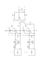
図1は本発明の好適な一実施の形態を示している。同図に示す回路はスイッチング電源の要部であり、トランスTを備えて、1次側に、2つのスイッチング素子S1,S2を配置してハーフブリッジとし、さらにインダクタLr,コンデンサCrを配置して共振タンク素子とし、2次側には2つの整流ダイオードD1,D2および平滑コンデンサCを配置し、ハーフブリッジ共振型コンバータの構成になっている。 FIG. 1 shows a preferred embodiment of the present invention. The circuit shown in the figure is a main part of the switching power supply, includes a transformer T, and arranges two switching elements S1 and S2 on the primary side to form a half bridge, and further includes an inductor Lr and a capacitor Cr. As a resonant tank element, two rectifier diodes D1 and D2 and a smoothing capacitor C are arranged on the secondary side to form a half-bridge resonant converter.
スイッチング素子S1,S2はMOSFETを用い、トランスTの1次側でハイサイドとローサイドとの縦列に接続する。そして、各ゲートはそれぞれゲートドライバ1,2へ接続して2つの制御信号(PWM1,PWM2)により交互にスイッチング動作するようになっている。ハイサイド側(MOSFET・S1)のドレインは電源V+へ接続し、ローサイド側(MOSFET・S2)のドレイン,ソース間にインダクタLr,トランスTの1次側,コンデンサCrを直列に接続して当該ソースは接地している。これにより、インダクタLr,コンデンサCrが直列の共振タンク素子を構成し、さらにトランスTの磁化インダクタンスがもう一つの共振周波数を生成することに機能し、いわゆるLLC共振型になっている。
The switching elements S1 and S2 use MOSFETs and are connected to the high side and low side columns on the primary side of the transformer T. The gates are connected to the
トランスTの2次側はセンタータップを有し、両端に整流ダイオードD1,D2をそれぞれ接続するとともに、それら整流ダイオードD1,D2の他端は共に接続して接地側とする。また、センタータップには平滑コンデンサCを接地側と並列に渡して接続し、当該センタータップ側が直流出力を取り出す正極ラインになる。 The secondary side of the transformer T has a center tap, and rectifier diodes D1 and D2 are connected to both ends, respectively, and the other ends of the rectifier diodes D1 and D2 are connected together to be a ground side. Further, a smoothing capacitor C is connected to the center tap in parallel with the ground side, and the center tap side becomes a positive line for taking out a DC output.
MOSFET・S1,S2は、ソース−ドレイン間に寄生ダイオードが存在する。すなわち、図中に点線で示す素子Dp1,Dp2が、それぞれの寄生ダイオードである。MOSFET・S1,S2の各ゲートとゲートドライバ1,2との間にはゲート抵抗(Rg11,Rg21)とゲートダイオード(Dg1,Dg2)とを直列に設けている。さらにゲートダイオード(Dg1,Dg2)にはゲート抵抗(Rg12,Rg22)を並列に接続している。ゲートドライバ1,2が出力する制御信号PWM1,PWM2は、パルス幅変調(PWM:Pulse Width Modulation)による駆動信号であり、制御信号PWM1と制御信号PWM2とは逆相の関係になる。
MOSFETs S1 and S2 have a parasitic diode between the source and the drain. That is, elements Dp1 and Dp2 indicated by dotted lines in the figure are the respective parasitic diodes. Between the gates of the MOSFETs S1 and S2 and the
スイッチング素子S1,S2の損失低減回路は、カレントトランスCT1,CT2とバイアス抵抗R1,R2とを備えて、MOSFET・S1,S2のドレインから流出する逆向き電流を検出し、逆向き電流の検出があるとき、MOSFET・S1,S2をオン動作させる構成になっている。 The loss reduction circuit of the switching elements S1 and S2 includes current transformers CT1 and CT2 and bias resistors R1 and R2, and detects the reverse current flowing out from the drains of the MOSFETs S1 and S2, thereby detecting the reverse current. In some cases, the MOSFETs S1 and S2 are turned on.
カレントトランスCT1,CT2はMOSFET・S1,S2のドレイン側の配線に配置し、接地側端子はソース側へ接続し、出力側端子をゲート側へ接続させていて、MOSFET・S1,S2のドレインから流出する逆向き電流を検出する動作を行い、ドレイン逆電流検出手段になっている。そして、バイアス抵抗R1,R2はMOSFET・S1,S2のゲート,ソースに渡して接続している。このため、カレントトランスCT1,CT2が検出信号を出力すると、検出信号はバイアス抵抗R1,R2を通りゲート電位が上がってMOSFET・S1,S2がオン動作し、バイアス抵抗R1,R2はMOSFET・S1,S2をオン動作させるオン駆動手段になっている。 The current transformers CT1 and CT2 are arranged on the wiring on the drain side of the MOSFETs S1 and S2, the ground side terminal is connected to the source side, the output side terminal is connected to the gate side, and from the drains of the MOSFETs S1 and S2. An operation for detecting the reverse current flowing out is performed and drain reverse current detection means is provided. The bias resistors R1 and R2 are connected to the gates and sources of the MOSFETs S1 and S2. For this reason, when the current transformers CT1 and CT2 output detection signals, the detection signals pass through the bias resistors R1 and R2, the gate potential rises, and the MOSFETs S1 and S2 are turned on. It is an on drive means for turning on S2.
ドレイン逆電流検出手段は、カレントトランスを備えて電流の検出を行う構成には限らない。例えばフォトカプラを備えて電流の検出を行う構成にしてもよく、適宜に構成できる。 The drain reverse current detection means is not limited to a configuration that includes a current transformer and detects current. For example, it may be configured to include a photocoupler and detect current, and can be configured appropriately.
(スイッチング動作)
ハイサイドのMOSFET・S1とローサイドのMOSFET・S2は交互にオン・オフ動作し、交互の切り替え動作では両者が同時にオフする期間(デッドタイム)を設ける動作になっている。MOSFET・S1がターンオンしてMOSFET・S2がオフ状態では図2(a)に示すように、電源V+から電流がMOSFET・S1,インダクタLr,トランスTの1次側,コンデンサCrの経路で接地へ流れる。次に、MOSFET・S1がターンオフしてMOSFET・S2がオフ状態のデッドタイム期間では図2(b)に示すように、トランスTの1次側で誘導起電力Viが誘起し、これによる誘導電流はコンデンサCr,寄生ダイオードDp2,インダクタLrの経路でトランスTの1次側へ戻り流れるが、このとき、カレントトランスCT2が誘導電流を検出するので、その検出信号によりゲート電位が上がってMOSFET・S2がターンオンする。このため、誘導電流はMOSFET・S2のオン抵抗を流通し、その結果、トランスTが蓄えたエネルギの放出が速やかに完了する動作になる。誘導電流の消滅によりMOSFET・S2がオフ状態に戻る。
(Switching operation)
The high-side MOSFET S1 and the low-side MOSFET S2 are alternately turned on and off, and in the alternate switching operation, a period (dead time) in which both are simultaneously turned off is provided. When the MOSFET S1 is turned on and the MOSFET S2 is in an OFF state, as shown in FIG. 2A, current is supplied from the power source V + to the ground through the path of the MOSFET S1, the inductor Lr, the transformer T, and the capacitor Cr. Flowing. Next, as shown in FIG. 2B, the induced electromotive force Vi is induced on the primary side of the transformer T in the dead time period in which the MOSFET S1 is turned off and the MOSFET S2 is turned off, and the induced current is thereby induced. Flows back to the primary side of the transformer T through the path of the capacitor Cr, the parasitic diode Dp2, and the inductor Lr. At this time, the current transformer CT2 detects the induced current. Turns on. For this reason, the induced current flows through the on-resistance of the MOSFET S2, and as a result, the operation of quickly releasing the energy stored in the transformer T is performed. The MOSFET S2 returns to the OFF state due to the disappearance of the induced current.
続いて、MOSFET・S1がオフ状態でMOSFET・S2がターンオンすると図2(c)に示すように、コンデンサCrの蓄積エネルギの放出が始まり電流はトランスTの1次側,インダクタLr,MOSFET・S2(オン抵抗)の経路で接地へ流れる。そして、MOSFET・S1がオフ状態でMOSFET・S2がターンオフするデッドタイム期間では図2(d)に示すように、トランスTの1次側で誘導起電力Viが誘起し、これによる誘導電流はインダクタLr,寄生ダイオードDp1の経路で電源V+側へ流れ出すが、このとき、カレントトランスCT1が誘導電流を検出するので、その検出信号によりゲート電位が上がってMOSFET・S1がターンオンする。このため、誘導電流はMOSFET・S1のオン抵抗を流通し、その結果、トランスTが蓄えたエネルギの放出が速やかに完了する動作になる。誘導電流の消滅によりMOSFET・S1がオフ状態に戻る。 Subsequently, when the MOSFET S1 is turned on while the MOSFET S1 is turned off, as shown in FIG. 2C, the stored energy of the capacitor Cr starts to be released, and the current is the primary side of the transformer T, the inductor Lr, the MOSFET S2 It flows to the ground via the (ON resistance) path. In a dead time period in which the MOSFET S1 is turned off and the MOSFET S2 is turned off, an induced electromotive force Vi is induced on the primary side of the transformer T as shown in FIG. Lr and the parasitic diode Dp1 flow to the power supply V + side. At this time, the current transformer CT1 detects the induced current, so that the detection signal causes the gate potential to rise and the MOSFET S1 is turned on. For this reason, the induced current flows through the ON resistance of the MOSFET S1, and as a result, the operation of quickly releasing the energy stored in the transformer T is performed. The MOSFET S1 returns to the OFF state due to the disappearance of the induced current.
このように、MOSFET・S1,S2のドレインから流出する逆向き電流(誘導電流)はドレイン逆電流検出手段が検出し、その逆向き電流の検出があるときはオン駆動手段が当該MOSFET・S1,S2をオン動作させるので、誘導電流はMOSFET・S1,S2のオン抵抗により流通させることができる。このため、寄生ダイオードDp1,Dp2を通る電流を抑制することができ、MOSFET・S1,S2のオン抵抗はきわめて小さく、トランスTが蓄えたエネルギの放出を速やかに完了できる。これにより、スイッチング動作に伴う逆向き電流による電力損失を低減でき、従来の構成に設けたバイパス用の高速ダイオード等は必要としない。 As described above, the reverse current (inductive current) flowing out from the drains of the MOSFETs S1 and S2 is detected by the drain reverse current detecting means, and when the reverse current is detected, the on-drive means is detected by the MOSFET S1, S1. Since the S2 is turned on, the induced current can be circulated by the on-resistances of the MOSFETs S1 and S2. For this reason, it is possible to suppress the current passing through the parasitic diodes Dp1 and Dp2, the on-resistances of the MOSFETs S1 and S2 are extremely small, and the release of the energy stored in the transformer T can be completed quickly. As a result, power loss due to the reverse current accompanying the switching operation can be reduced, and a bypass high-speed diode or the like provided in the conventional configuration is not required.
計算例を示すと、MOSFET・S1,S2の特性はオン抵抗Ronが0.38[Ω]程度であり、誘導電流Isが例えばピーク値で2[A]であるときは、電力損失Plossは、
Ploss = Ron×Is2 = 0.38×(2÷√3)2 = 0.51[W]
となる。従来の構成では寄生ダイオードDp1,Dp2に流通するので、寄生ダイオードDp1,Dp2の特性は順方向電圧Vsdが1.4[V]程度であり、このため誘導電流Is=2[A]ピーク値では電力損失Plossは、
Ploss = Vsd×Is = 1.4×2÷√3 = 1.62[W]
となり、従来との差が1.11[W]であることがわかる。すなわち、従来と比べて電力損失は約1/3以下に低減することができる。したがって本発明にあっては、電力損失を低減できることから高効率を得ることができ、MOSFET(スイッチング素子S1,S2)の発熱を減らすことができる。その結果、当該素子へ組み付ける放熱器を小型化あるいは不要にすることができ、これにより装置の小型化がよりさらに行える。
As a calculation example, when the on-resistance Ron is about 0.38 [Ω] and the induced current Is has a peak value of 2 [A], for example, the characteristics of the MOSFETs S1 and S2 are:
Ploss = Ron × Is 2 = 0.38 × (2 ÷ √3) 2 = 0.51 [W]
It becomes. In the conventional configuration, since the parasitic diodes Dp1 and Dp2 are distributed, the characteristics of the parasitic diodes Dp1 and Dp2 are such that the forward voltage Vsd is about 1.4 [V], and therefore the induced current Is = 2 [A] peak value The power loss Ploss is
Ploss = Vsd × Is = 1.4 × 2 ÷ √3 = 1.62 [W]
Thus, it can be seen that the difference from the prior art is 1.11 [W]. That is, the power loss can be reduced to about 1/3 or less compared to the conventional case. Therefore, in the present invention, since power loss can be reduced, high efficiency can be obtained, and heat generation of MOSFETs (switching elements S1, S2) can be reduced. As a result, it is possible to reduce or eliminate the heat radiator to be assembled to the element, thereby further reducing the size of the device.
1,2 ゲートドライバ
C 平滑コンデンサ
Cr コンデンサ
CT1,CT2 カレントトランス
D1,D2 整流ダイオード
Dg1,Dg2 ゲートダイオード
Lr インダクタ
R1,R2 バイアス抵抗
Rg11,Rg12,Rg21,Rg22 ゲート抵抗
S1,S2 スイッチング素子(MOSFET)
T トランス
Vi 誘導起電力
1, 2 Gate driver C Smoothing capacitor Cr Capacitor CT1, CT2 Current transformer D1, D2 Rectifier diode Dg1, Dg2 Gate diode Lr Inductor R1, R2 Bias resistance Rg11, Rg12, Rg21, Rg22 Gate resistance S1, S2 Switching element (MOSFET)
T transformer Vi Inductive electromotive force
Claims (2)
前記MOSFETのドレインから流出する逆向き電流を検出するドレイン逆電流検出手段と、前記ドレイン逆電流検出手段から検出信号を受けて前記MOSFETをオン動作させるオン駆動手段とを備え、
前記ドレイン逆電流検出手段は、前記MOSFETのドレイン側の配線に配置したカレントトランスを備え、
前記カレントトランスの接地側端子は前記MOSFETのソース側へ接続し、前記カレントトランスの出力側端子は前記MOSFETのゲート側に接続することを特徴とするスイッチング素子の損失低減回路。 A switching element loss reduction circuit for suppressing a loss due to a reverse current caused by a switching operation, wherein the switching element is a MOSFET, and the high side and low side switching elements are connected to an inductive load and alternately turned on. -In a bridge circuit that is turned off,
A drain reverse current detection means for detecting a reverse current flowing out from the drain of the MOSFET; and an on drive means for receiving a detection signal from the drain reverse current detection means to turn on the MOSFET,
The drain reverse current detection means includes a current transformer disposed on a wiring on the drain side of the MOSFET ,
A loss reduction circuit for a switching element, wherein a ground side terminal of the current transformer is connected to a source side of the MOSFET, and an output side terminal of the current transformer is connected to a gate side of the MOSFET .
Priority Applications (1)
| Application Number | Priority Date | Filing Date | Title |
|---|---|---|---|
| JP2009064257A JP5522824B2 (en) | 2009-03-17 | 2009-03-17 | Switching element loss reduction circuit |
Applications Claiming Priority (1)
| Application Number | Priority Date | Filing Date | Title |
|---|---|---|---|
| JP2009064257A JP5522824B2 (en) | 2009-03-17 | 2009-03-17 | Switching element loss reduction circuit |
Publications (2)
| Publication Number | Publication Date |
|---|---|
| JP2010220385A JP2010220385A (en) | 2010-09-30 |
| JP5522824B2 true JP5522824B2 (en) | 2014-06-18 |
Family
ID=42978610
Family Applications (1)
| Application Number | Title | Priority Date | Filing Date |
|---|---|---|---|
| JP2009064257A Active JP5522824B2 (en) | 2009-03-17 | 2009-03-17 | Switching element loss reduction circuit |
Country Status (1)
| Country | Link |
|---|---|
| JP (1) | JP5522824B2 (en) |
Families Citing this family (3)
| Publication number | Priority date | Publication date | Assignee | Title |
|---|---|---|---|---|
| JP6673651B2 (en) * | 2015-06-30 | 2020-03-25 | ダイハツ工業株式会社 | Power supply for plasma reactor |
| EP3576269A1 (en) * | 2018-05-29 | 2019-12-04 | Siemens Aktiengesellschaft | Control of a metal oxide semiconductor field effect transistor |
| CN114024432B (en) * | 2021-11-16 | 2023-10-27 | 西安电子科技大学 | A gate crosstalk suppression circuit for SiC MOSFET power devices |
Family Cites Families (8)
| Publication number | Priority date | Publication date | Assignee | Title |
|---|---|---|---|---|
| JPS63185220A (en) * | 1987-01-28 | 1988-07-30 | Mitsubishi Electric Corp | Driving circuit for cascode type bimos |
| JP3066727B2 (en) * | 1995-12-20 | 2000-07-17 | 富士通電装株式会社 | Synchronous rectification drive circuit |
| JP2001016872A (en) * | 1999-06-24 | 2001-01-19 | Yokogawa Electric Corp | Switching control circuit |
| JP2002142447A (en) * | 2000-10-31 | 2002-05-17 | Sony Corp | Power supply and electronic equipment |
| US6529034B1 (en) * | 2001-11-07 | 2003-03-04 | International Rectifier Corporation | Integrated series schottky and FET to allow negative drain voltage |
| JP2007014059A (en) * | 2005-06-28 | 2007-01-18 | Toyota Motor Corp | Switching circuit |
| JP2007274789A (en) * | 2006-03-30 | 2007-10-18 | Densei Lambda Kk | Switching power supply device |
| JP2007312522A (en) * | 2006-05-18 | 2007-11-29 | Sony Corp | Switching power supply circuit |
-
2009
- 2009-03-17 JP JP2009064257A patent/JP5522824B2/en active Active
Also Published As
| Publication number | Publication date |
|---|---|
| JP2010220385A (en) | 2010-09-30 |
Similar Documents
| Publication | Publication Date | Title |
|---|---|---|
| JP4803262B2 (en) | Isolated switching power supply | |
| CN104052296B (en) | System and method for switched mode power converter | |
| CN101795076B (en) | Power converter and method for controlling power converter | |
| EP1356575A2 (en) | Isolated drive circuitry used in switch-mode power converters | |
| US20110090725A1 (en) | Systems and Methods of Synchronous Rectifier Control | |
| JP2005304294A (en) | Method for utilizing source inductance common with synchronous rectification ciruit and synchronous fet | |
| US20080037290A1 (en) | Ac-dc converter and method for driving for ac-dc converter | |
| CN102239628A (en) | Switching power converter for reducing EMI from ring oscillations and control method thereof | |
| JP5326605B2 (en) | Power converter | |
| US7285876B1 (en) | Regenerative gate drive circuit for power MOSFET | |
| CN111800014B (en) | Switching Converters | |
| US20120013369A1 (en) | Synchronous Rectifier Gate Drive Timing To Compensate For Transformer Leakage Inductance | |
| US6859372B2 (en) | Bridge-buck converter with self-driven synchronous rectifiers | |
| US6788553B1 (en) | Switching-mode power converter with complementary synchronous rectification | |
| JP5522824B2 (en) | Switching element loss reduction circuit | |
| Nymand et al. | A new approach to high efficiency in isolated boost converters for high-power low-voltage fuel cell applications | |
| KR20190064962A (en) | DC to DC Converting System | |
| JP5697255B2 (en) | Semi-bridgeless power factor correction circuit and driving method of semi-bridgeless power factor correction circuit | |
| WO2010143124A1 (en) | A limiting circuit for an active clamp and a method of controlling a converter having a limiting circuit | |
| JP2013135570A (en) | Dc-dc converter | |
| JP4107172B2 (en) | DC-DC converter device | |
| US11764698B2 (en) | RCD buffer circuit for a rectifier on a flyback secondary | |
| EP2239835B1 (en) | Converter device and corresponding method | |
| US20020067140A1 (en) | Push-pull based voltage-clamping electronic ballast | |
| WO2022097561A1 (en) | Dc/dc converter |
Legal Events
| Date | Code | Title | Description |
|---|---|---|---|
| A621 | Written request for application examination |
Free format text: JAPANESE INTERMEDIATE CODE: A621 Effective date: 20120217 |
|
| A977 | Report on retrieval |
Free format text: JAPANESE INTERMEDIATE CODE: A971007 Effective date: 20130621 |
|
| A131 | Notification of reasons for refusal |
Free format text: JAPANESE INTERMEDIATE CODE: A131 Effective date: 20130704 |
|
| A521 | Request for written amendment filed |
Free format text: JAPANESE INTERMEDIATE CODE: A523 Effective date: 20130829 |
|
| TRDD | Decision of grant or rejection written | ||
| A01 | Written decision to grant a patent or to grant a registration (utility model) |
Free format text: JAPANESE INTERMEDIATE CODE: A01 Effective date: 20140403 |
|
| A61 | First payment of annual fees (during grant procedure) |
Free format text: JAPANESE INTERMEDIATE CODE: A61 Effective date: 20140407 |
|
| R150 | Certificate of patent or registration of utility model |
Ref document number: 5522824 Country of ref document: JP Free format text: JAPANESE INTERMEDIATE CODE: R150 |
|
| S531 | Written request for registration of change of domicile |
Free format text: JAPANESE INTERMEDIATE CODE: R313531 |
|
| R350 | Written notification of registration of transfer |
Free format text: JAPANESE INTERMEDIATE CODE: R350 |
|
| R250 | Receipt of annual fees |
Free format text: JAPANESE INTERMEDIATE CODE: R250 |
|
| R250 | Receipt of annual fees |
Free format text: JAPANESE INTERMEDIATE CODE: R250 |
|
| R250 | Receipt of annual fees |
Free format text: JAPANESE INTERMEDIATE CODE: R250 |
|
| R250 | Receipt of annual fees |
Free format text: JAPANESE INTERMEDIATE CODE: R250 |
|
| R250 | Receipt of annual fees |
Free format text: JAPANESE INTERMEDIATE CODE: R250 |
|
| R250 | Receipt of annual fees |
Free format text: JAPANESE INTERMEDIATE CODE: R250 |
|
| R250 | Receipt of annual fees |
Free format text: JAPANESE INTERMEDIATE CODE: R250 |
|
| R250 | Receipt of annual fees |
Free format text: JAPANESE INTERMEDIATE CODE: R250 |
|
| R250 | Receipt of annual fees |
Free format text: JAPANESE INTERMEDIATE CODE: R250 |
|
| R250 | Receipt of annual fees |
Free format text: JAPANESE INTERMEDIATE CODE: R250 |