JP5146618B1 - Method for manufacturing light emitting device - Google Patents
Method for manufacturing light emitting device Download PDFInfo
- Publication number
- JP5146618B1 JP5146618B1 JP2012123336A JP2012123336A JP5146618B1 JP 5146618 B1 JP5146618 B1 JP 5146618B1 JP 2012123336 A JP2012123336 A JP 2012123336A JP 2012123336 A JP2012123336 A JP 2012123336A JP 5146618 B1 JP5146618 B1 JP 5146618B1
- Authority
- JP
- Japan
- Prior art keywords
- cutting
- semiconductor wafer
- light emitting
- rotary blade
- cuts
- Prior art date
- Legal status (The legal status is an assumption and is not a legal conclusion. Google has not performed a legal analysis and makes no representation as to the accuracy of the status listed.)
- Expired - Fee Related
Links
- 238000004519 manufacturing process Methods 0.000 title claims abstract description 22
- 238000000034 method Methods 0.000 title claims description 17
- 238000005520 cutting process Methods 0.000 claims abstract description 245
- 239000004065 semiconductor Substances 0.000 claims abstract description 114
- 235000012431 wafers Nutrition 0.000 claims description 128
- XLYOFNOQVPJJNP-UHFFFAOYSA-N water Substances O XLYOFNOQVPJJNP-UHFFFAOYSA-N 0.000 claims description 41
- 238000007599 discharging Methods 0.000 claims description 9
- 238000002360 preparation method Methods 0.000 claims description 8
- 238000003860 storage Methods 0.000 description 11
- 230000032258 transport Effects 0.000 description 6
- 230000002093 peripheral effect Effects 0.000 description 4
- 230000008602 contraction Effects 0.000 description 2
- 230000015572 biosynthetic process Effects 0.000 description 1
- 238000010586 diagram Methods 0.000 description 1
- 239000012634 fragment Substances 0.000 description 1
- 230000004048 modification Effects 0.000 description 1
- 238000012986 modification Methods 0.000 description 1
- 239000008188 pellet Substances 0.000 description 1
- 238000001179 sorption measurement Methods 0.000 description 1
Images




Landscapes
- Dicing (AREA)
Abstract
【課題】半導体ウエハを切断して発光素子を製造する際に、発光点が損傷するのを抑制することができる発光素子の製造方法を得る。
【解決手段】発光素子30における発光点30Aの列に沿った一方の縁辺を形成させた後に、一方の縁辺に対して規定間隔を空けて半導体ウエハ22を切断して、一方の縁辺30Bに比して発光点30Aとは離れた発光素子30の他方の縁辺30Cを形成させる。このように、一方の縁辺30Bに比して発光点30Aの列とは離れた他方の縁辺30Cを形成させて発光素子30を半導体ウエハ22から切り離すことで、他方の縁辺30Cを形成される際に、半導体ウエハ22から切り離される側の発光素子30がばたついても、ブレード46と発光点30Aとが離れているため、発光点30Aの損傷が抑制される。
【選択図】図4A method of manufacturing a light emitting element capable of suppressing damage of a light emitting point when a light emitting element is manufactured by cutting a semiconductor wafer.
After forming one edge along a row of light emitting points 30A in a light emitting element 30, a semiconductor wafer 22 is cut at a predetermined interval with respect to the one edge, and compared with one edge 30B. Thus, the other edge 30C of the light emitting element 30 separated from the light emitting point 30A is formed. As described above, when the other edge 30C is formed by separating the light emitting element 30 from the semiconductor wafer 22 by forming the other edge 30C far from the row of light emitting points 30A as compared to the one edge 30B. Even if the light emitting element 30 on the side separated from the semiconductor wafer 22 flutters, damage to the light emitting point 30A is suppressed because the blade 46 and the light emitting point 30A are separated from each other.
[Selection] Figure 4
Description
本発明は、発光素子の製造方法に関する。 The present invention relates to a method for manufacturing a light emitting device.
特許文献1には、切断によって形成されたペレットの飛散によって生ずる切削ブレードの破損を防止することができるダイシング方法が記載されている。 Patent Document 1 describes a dicing method that can prevent breakage of a cutting blade caused by scattering of pellets formed by cutting.
具体的には、所定角度をもってして形成された複数個の第1のストリートと第2のストリートとを有する被加工物を、切削ブレードにより、第1のストリートおよび第2のストリートに沿って切断するダイシング方法であって、第1のストリートを切断した後に第2のストリートを切断するときには、切削ブレードの基台側が被加工物の未加工領域側に向くように切断するようになっている。 Specifically, a workpiece having a plurality of first streets and second streets formed at a predetermined angle is cut along the first and second streets by a cutting blade. In this dicing method, when the second street is cut after the first street is cut, the base side of the cutting blade is cut toward the unprocessed region side of the workpiece.
本発明の課題は、半導体ウエハを切断して発光素子を製造する際に、発光点が損傷するのを抑制することである。 An object of the present invention is to suppress damage of a light emitting point when a light emitting element is manufactured by cutting a semiconductor wafer.
本発明の請求項1に係る発光素子の製造方法は、長方形状とされると共に長手方向の一方の緑辺に沿って他方の縁辺に比して近くなるように一列に並ぶ発光点が複数形成される発光素子を複数製造するために、前記発光点の列を予め規定された規定間隔で複数形成させた半導体ウエハを固定台に固定する準備工程と、前記準備工程で、前記固定台に固定された前記半導体ウエハを、前記発光点の列に沿って切断して前記発光素子の前記一方の縁辺を形成させた後に、前記一方の縁辺に対して前記規定間隔を空けて前記半導体ウエハを切断して他方の縁辺を形成させる第一切断工程と、前記第一切断工程の後、前記固定台に固定された前記半導体ウエハを、回転刃を用いて前記長手方向に対して交差する短手方向に沿って切断して前記半導体ウエハから前記発光素子を切り出す第二切断工程と、を備え、前記第一切断工程では、予め決められた総切断回数だけ、前記回転刃を構成する第一回転刃を用いて前記半導体ウエハの前記長手方向を切断すると共に、第一吐出部材を用いて前記第一回転刃に向けて切削水を吐出し、前記第一回転刃が前記半導体ウエハを切断している際に、前記総切断回数に対して残りの残切断回数又は既に前記半導体ウエハを切断した既切断回数を計数部材が数え、前記第二切断工程では、 回転しながら前記半導体ウエハを切断する前記回転刃を構成する第二回転刃を用いて前記半導体ウエハの前記短手方向を切断すると共に、第二吐出部材を用いて前記第二回転刃に向けて切削水を吐出し、前記第一切断工程の際に、前記計数部材によって数えられた前記残切断回数又は前記既切断回数が、決められた回数に達するまでは、前記第二吐出部材からの切削水の吐出を停止させ、前記残切断回数又は前記既切断回数が、前記決められた回数に達した後に、前記第二吐出部材から切削水を吐出させて前記第二回転刃の温度を予め定められた範囲内とすることを特徴とする。 According to a first aspect of the present invention, there is provided a method for manufacturing a light-emitting element, wherein a plurality of light-emitting points arranged in a row are formed in a rectangular shape along one green side in the longitudinal direction so as to be closer to the other side. In order to manufacture a plurality of light emitting elements to be manufactured, a preparation step of fixing a semiconductor wafer in which a plurality of rows of light emitting points are formed at a predetermined interval specified in advance to a fixing base, and fixing to the fixing base in the preparation step The semiconductor wafer is cut along the row of light emitting points to form the one edge of the light emitting element, and then the semiconductor wafer is cut with a predetermined interval from the one edge. The first cutting step of forming the other edge, and the short side direction that intersects the longitudinal direction with the rotary blade after the first cutting step using a rotary blade Cut along the semiconductor wafer. And a second cutting step of cutting said light emitting element from Ha, in the first cutting step, only the total number of cuts to a predetermined, said the semiconductor wafer using a first rotary blade constituting the rotary blade Cutting the longitudinal direction and discharging cutting water toward the first rotary blade using the first discharge member, and when the first rotary blade is cutting the semiconductor wafer, the total number of cuts The counter member counts the remaining number of remaining cuts or the number of previous cuts that have already been performed on the semiconductor wafer, and in the second cutting step, the second rotary blade constituting the rotary blade that cuts the semiconductor wafer while rotating And cutting the transverse direction of the semiconductor wafer using the second discharge member and discharging the cutting water toward the second rotary blade using the second discharge member, and by the counting member during the first cutting step The remaining counted Until the number of cuttings or the number of already cuts reaches a predetermined number of times, the discharge of cutting water from the second discharge member is stopped, and the number of remaining cuttings or the number of already cuts is set to the predetermined number of times. After reaching, the cutting water is discharged from the second discharge member, and the temperature of the second rotary blade is set within a predetermined range.
本発明の請求項2に係る発光素子の製造方法は、長方形状とされると共に長手方向の一方の緑辺に沿って他方の縁辺に比して近くなるように一列に並ぶ発光点が複数形成される発光素子を複数製造するために、前記発光点の列を予め規定された規定間隔で複数形成させた半導体ウエハを固定台に固定する準備工程と、前記準備工程で、前記固定台に固定された前記半導体ウエハを、前記発光点の列に沿って切断して前記発光素子の前記一方の縁辺を形成させた後に、前記一方の縁辺に対して前記規定間隔を空けて前記半導体ウエハを切断して他方の縁辺を形成させる第一切断工程と、前記第一切断工程の後、前記固定台に固定された前記半導体ウエハを、回転刃を用いて前記長手方向に対して交差する短手方向に沿って切断して前記半導体ウエハから前記発光素子を切り出す第二切断工程と、を備え、前記第一切断工程では、 予め決められた総切断回数だけ、前記回転刃を構成する第一回転刃を用いて前記半導体ウエハの前記長手方向を切断すると共に、第一吐出部材を用いて前記第一回転刃に向けて切削水を吐出し、前記第一回転刃が前記半導体ウエハを切断している際に、前記総切断回数に対して残りの残切断回数又は既に前記半導体ウエハを切断した既切断回数を計数部材が数え、前記第二切断工程では、回転しながら前記半導体ウエハを切断する前記回転刃を構成する第二回転刃を用いて前記半導体ウエハの前記短手方向を切断すると共に、第二吐出部材を用いて前記第二回転刃に向けて切削水を吐出し、前記第一切断工程の際に、前記計数部材によって数えられた前記残切断回数又は前記既切断回数が、決められた回数に達するまでは、前記第二吐出部材からの切削水の吐出及び前記第二回転刃の回転を停止させ、前記残切断回数又は前記既切断回数が、前記決められた回数に達した後に、前記第二吐出部材から切削水を吐出させると共に前記第二回転刃を回転させて前記第二回転刃の温度を予め定められた範囲内とすることを特徴とする。 According to a second aspect of the present invention, there is provided a method for manufacturing a light emitting device, wherein a plurality of light emitting points are formed in a line so as to be rectangular and to be closer to one edge along the green side in the longitudinal direction than the other edge. In order to manufacture a plurality of light emitting elements to be manufactured, a preparation step of fixing a semiconductor wafer in which a plurality of rows of light emitting points are formed at a predetermined interval specified in advance to a fixing base, and fixing to the fixing base in the preparation step The semiconductor wafer is cut along the row of light emitting points to form the one edge of the light emitting element, and then the semiconductor wafer is cut with a predetermined interval from the one edge. The first cutting step of forming the other edge, and the short side direction that intersects the longitudinal direction with the rotary blade after the first cutting step using a rotary blade Cut along the semiconductor wafer. A second cutting step of cutting out the light emitting element from c, wherein the first cutting step uses the first rotary blade constituting the rotary blade for a predetermined total number of times of cutting. Cutting the longitudinal direction and discharging cutting water toward the first rotary blade using the first discharge member, and when the first rotary blade is cutting the semiconductor wafer, the total number of cuts In contrast, the counting member counts the number of remaining remaining cuts or the number of cuts that have already been performed on the semiconductor wafer. In the second cutting step, the second rotary blade constituting the rotary blade that cuts the semiconductor wafer while rotating. And cutting the transverse direction of the semiconductor wafer using the second discharge member and discharging the cutting water toward the second rotary blade using the second discharge member, and by the counting member during the first cutting step The remaining counted Until the number of cuts or the number of previous cuts reaches a predetermined number of times, the discharge of the cutting water from the second discharge member and the rotation of the second rotary blade are stopped, the number of remaining cuts or the number of previous cuts However, after reaching the predetermined number of times, the cutting water is discharged from the second discharge member and the second rotary blade is rotated so that the temperature of the second rotary blade is within a predetermined range. It is characterized by.
本発明の請求項1の発光素子の製造方法によれば、第二回転刃が半導体ウエハを切断する切断状態となるまで、第二吐出部材からの切削水の吐出を停止させる場合と比して、切削水の消費を抑制した上で、第二回転刃を切断状態とする際に、切断位置がずれてしまうのを抑制することができる。 According to the method for manufacturing a light emitting element of claim 1 of the present invention, as compared with the case where the discharge of the cutting water from the second discharge member is stopped until the second rotary blade is in a cutting state for cutting the semiconductor wafer. In addition, it is possible to prevent the cutting position from shifting when the second rotary blade is in a cutting state while suppressing consumption of the cutting water.
本発明の請求項2の発光素子の製造方法によれば、第二回転刃が半導体ウエハを切断する切断状態となるまで、第二吐出部材からの切削水の吐出、及び第二回転刃の回転を停止させる場合と比して、切削水の消費を抑制した上で、第二回転刃を切断状態とする際に、切断位置がずれてしまうのを抑制することができる。 According to the method for manufacturing a light emitting element of claim 2 of the present invention, the cutting water is discharged from the second discharge member and the second rotating blade is rotated until the second rotating blade is in a cutting state for cutting the semiconductor wafer. As compared with the case where the cutting is stopped, the cutting position can be prevented from shifting when the cutting blade is consumed and the second rotary blade is cut.
本発明の実施形態に係る発光素子の製造方法の一例について図1〜図15に従って説明する。先ず、この発光素子の製造方法に用いられるウエハ切断装置について説明する。なお、図中に示す矢印Zは、鉛直方向上方を示す。 An example of a method for manufacturing a light emitting device according to an embodiment of the present invention will be described with reference to FIGS. First, a wafer cutting apparatus used in this method for manufacturing a light emitting element will be described. In addition, the arrow Z shown in a figure shows the perpendicular direction upper direction.
(全体構成)
図14に示されるように、ウエハ切断装置10(ダイシング装置)は、半導体ウエハ22が積載される収納ボックス18と、切断される半導体ウエハ22が固定される固定台の一例としてのチャックテーブル12と、収納ボックス18に収納されている半導体ウエハ22をチャックテーブル12に搬送する搬送ユニット14と、チャックテーブル12を移動させる移動ユニット32と、移動ユニット32によって移動するチャックテーブル12に固定された半導体ウエハ22を切断する切断ユニット35と、切断ユニット35に向けて切削水を吐出する吐出ユニット60と、を含んで構成されている。
(overall structure)
As shown in FIG. 14, the wafer cutting apparatus 10 (dicing apparatus) includes a
〔収納ボックス〕
ウエハ切断装置10の筐体20は、直方体状とされた本体部位20Aと、本体部位20Aの一端側から鉛直方向上方に突出した突出部位20Bと、を備えている。
〔Storage box〕
The
半導体ウエハ22が積載される収納ボックス18は、本体部位20Aの他端側の角部に配置され、収納ボックス18の上部は開放されている。
The
また、収納ボックス18には、積載された半導体ウエハ22を昇降させる図示せぬ昇降部材が備えられており、最上位の半導体ウエハ22が一定の位置に配置されるようになっている。
The
〔半導体ウエハ〕
収納ボックス18に収納される半導体ウエハ22は、円形の一部が切りかかれた形状とされ、図12に示されるように、ダイシングテープ26の上に貼り付けられている。さらに、このダイシングテープ26の外周側は、リング状の基本リング28に貼り付けられている。このように、半導体ウエハ22は、基本リング28にダイシングテープ26を介して支持された状態で、前述した収納ボックス18に積載されている。
[Semiconductor wafer]
The
また、図中の半導体ウエハ22に記載されている二点鎖線は、切断ユニット16によって切断される切断位置である。この二点差線からも分かるように、半導体ウエハ22を切断ユニット16によって切断することで製造される半導体素子の一例としての発光素子30は、長方形状とされる。
In addition, a two-dot chain line described in the
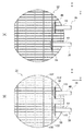
この発光素子30には、図11に示されるように、長手方向の一方の緑辺30Bに沿って、他方の縁辺30Cに比して近くなるように一列に並ぶ発光点30Aが複数形成されている。このような、発光素子30を製造するため、半導体ウエハ22には、図4に示されるように、発光点30Aの列が予め規定された規定間隔(図中に示す間隔H)で複数形成されている。
As shown in FIG. 11, the
〔搬送ユニット〕
チャックテーブル12に半導体ウエハ22を搬送する搬送ユニット14は、図14に示されるように、基端部が突出部位20Bの内部に支持されると共に水平方向に移動可能とされるアーム部位14Aと、アーム部位14Aの先端部に基端部が取り付けられると共に鉛直方向に伸縮可能とされる伸縮部位14Bと、伸縮部位14Bの先端部に取り付けられると共に基本リング28を吸着する吸着部位14Cと、を備えている。
[Transport unit]
As shown in FIG. 14, the transfer unit 14 that transfers the
この構成により、搬送ユニット14は、収納ボックス18に収容された最上位の半導体ウエハ22を、基本リング28を介して持ち上げてチャックテーブル12に向けて搬送するようになっている。
With this configuration, the transport unit 14 lifts the uppermost semiconductor wafer 22 stored in the
〔チャックテーブル〕
チャックテーブル12は、図10に示されるように、半導体ウエハ22を下方から支持する支持部位12Aを備えている。支持部位12Aは、平面視で円形状とされ、支持部位12Aには、半導体ウエハ22を、ダイシングテープ26を介して吸着するための図示せぬ吸引孔が複数形成されている。
[Chuck table]
As shown in FIG. 10, the chuck table 12 includes a
さらに、チャックテーブル12は、支持部位12Aを支持部位12Aの周方向に回転移動させる回転移動装置24を、支持部位12Aの下側に備えている。
Further, the chuck table 12 includes a
〔移動ユニット〕
また、図14に示されるように、チャックテーブル12を、搬送ユニット14によって搬送される半導体ウエハ22を受け取り可能な受取可能位置(図14参照)と、切断ユニット16によって半導体ウエハ22が切断可能とされる切断可能位置と、の間で移動させる前述した移動ユニット32が備えられている。
[Mobile unit]
Further, as shown in FIG. 14, the chuck table 12 can receive the
移動ユニット32は、鉛直方向に対して直交する第一方向(図中矢印X方向)にチャックテーブル12を移動させるようになっている。そして、移動ユニット32が、切断可能位置に配置されたチャックテーブル12を第一方向に往復移動させることで、切断ユニット16によって半導体ウエハ22が切断されるようになっている。
The moving
なお、半導体ウエハ22を切断する工程については、詳細を後述する。
Details of the process of cutting the
〔切断ユニット〕
切断ユニット35は、切断可能位置に配置されたチャックテーブル12の鉛直方向の上方に配置され、図13、図14に示されるように、第一回転刃の一例としての第一切断ユニット36と、第一切断ユニット36の隣に配置された第二回転刃の一例としての第二切断ユニット38と、を備えている。第一切断ユニット36と第二切断ユニット38とは、同様の構成であるため、ここでは、第一切断ユニット36について具体的に説明し、第二切断ユニット38の説明は省略する。
[Cut unit]
The cutting
第一切断ユニット36は、円筒状のハウジング40によって回転可能に支持されたスピンドル42と、スピンドル42の先端に取り付けられたフランジ44によって固定される円形のブレード46と、ブレード46を上方から覆うカバー部材70と、を備えている。
The
ハウジング40は、鉛直方向及び第一方向に対して直交する第二方向(図中矢印Y方向)に延びる円筒状に形成されている。また、ハウジング40の基端側には、ハウジング40の基端部を支持する駆動ユニット48が備えられている。
The
この駆動ユニット48が、ハウジング40を鉛直方向(Z方向)及び第二方向(Y方向)に移動させると共に、スピンドル42を介して半導体ウエハ22を切断するためのブレード46を回転させるようになっている。
The
具体的に鉛直方向(Z方向)については、駆動ユニット48は、ブレード46を用いて半導体ウエハ22を切断可能な稼動位置(図6(A)参照)と、ブレード46を半導体ウエハ22から退避させる退避位置(図6(B)参照)とにハウジング40を移動させるようになっている。
Specifically, in the vertical direction (Z direction), the
具体的に第二方向(Y方向)については、駆動ユニット48は、第一切断ユニット36を第二方向に移動させて、第二方向における半導体ウエハ22の切断位置を変えるようになっている(図4参照)。
Specifically, in the second direction (Y direction), the
この第一切断ユニット36に備えられた各部材と同様に、第二切断ユニット38は、ハウジング50と、スピンドル52と、フランジ54と、ブレード56と、駆動ユニット58と、カバー部材72と、を備えている。
Like each member provided in the
〔吐出ユニット〕
切削水を吐出する吐出ユニット60は、第一切断ユニット36に向けて切削水を吐出する第一吐出部材の一例としての第一吐出ユニット62と、第二切断ユニット38に向けて切削水を吐出する第二吐出部材の一例としての第二吐出ユニット64と、を備えている。
[Discharge unit]
The discharge unit 60 that discharges the cutting water discharges the cutting water toward the
第一吐出ユニット62と第二吐出ユニット64とは、同様の構成であるため、ここでは、第一吐出ユニット62について具体的に説明する。
Since the
第一吐出ユニット62は、図2、図3に示されるように、ブレード46の表面及び裏面に向けて切削水を吐出する吐出管72A及び吐出管72Bと、ブレード46の外周端面に向けて切削水を吐出する吐出管74と、ブレード46によって切断される半導体ウエハ22の切断部位に向けて切削水を吐出する一対の吐出管76と、を備えている。そして、吐出管72A、72B、吐出管74、及び吐出管76は、カバー部材70に固定されており、第一切断ユニット36の移動に伴って一緒に移動するようになっている。
As shown in FIGS. 2 and 3, the
吐出管72A、72Bは、図3に示されるように、第二方向から見て、第一方向に延びるように配置され、吐出管72Aは、ブレード46の表面(フランジ44が配置される側の面)と対向するように配置され、吐出管72Bは、ブレード46の裏面と対向するように配置されている。
As shown in FIG. 3, the
吐出管72A、72Bには、図2に示されるように、ブレード46の表面又は裏面と対向するように複数の開孔73が形成されている。そして、吐出管72A、72Bを流れる切削水は、吐出管72A、72Bの先端部及び開孔73から、ブレード46の表面及び裏面に向けて吐出されるようになっている。
As shown in FIG. 2, a plurality of
吐出管74の先端部は、図2、図3に示されるように、ブレード46の外周端面と対向している。これにより、吐出管74を流れる切削水は、吐出管74の先端部から、ブレード46の外周端面に向けて吐出されるようになっている。
As shown in FIGS. 2 and 3, the distal end portion of the
一対の吐出管76は、図2に示されるように、第二方向において、吐出管74を挟むように配置されている。そして、吐出管76の先端部は、図3に示されるように、ブレード46によって切断される半導体ウエハ22の切断部位に対向している。これにより、吐出管76を流れる切削水は、吐出管76の先端部から半導体ウエハ22の切断部位に向けて吐出されるようになっている。
As shown in FIG. 2, the pair of
さらに、吐出管72A、72B、吐出管74、及び吐出管76には、図1に示されるように、バルブ78A、78B、バルブ80、及びバルブ82が接続され、バルブ78A、78B、バルブ80、及びバルブ82を介して切削水が供給されるようになっている。そして、各バルブの開閉は、後述する制御部材の一例としての制御部84によって制御されるようになっている。
Further, as shown in FIG. 1,
この第一吐出ユニット62と同様に、第二吐出ユニット64は、吐出管86A、86B、吐出管88及び吐出管90、並びにバルブ92A、92B、バルブ94及びバルブ96を備えている。
Similar to the
〔計数部材〕
前述した第一切断ユニット36は、支持部位12Aに固定された半導体ウエハ22を、予め決められた総切断回数(一枚の半導体ウエハ22において第一方向に切断する合計回数)だけ回転しながら切断するようになっている。そして、第一切断ユニット36が半導体ウエハ22を切断している際に、前述した総切断回数に対して残りの残切断回数を数える計数部材34(図5参照)が、ウエハ切断装置10に備えられている。
[Counting member]
The above-described first cutting
〔制御部〕
ウエハ切断装置10は、チャックテーブル12の支持部位12Aを回転移動させる回転移動装置24(図10参照)と、チャックテーブル12を第一方向に移動させる移動ユニット32(図14参照)と、第一切断ユニット36に備えられた駆動ユニット48と、第二切断ユニット36に備えられた駆動ユニット58(図13参照)と、各バルブの開閉と、を制御する制御部84を備えている(図5参照)。
(Control part)
The
また、この制御部84は、図5に示されるように、計数部材34によって数えられた残切断回数に基づいて、バルブ92A、92B、バルブ94及びバルブ96を制御して、第二吐出ユニット64から切削水を吐出させるようになっている。
Further, as shown in FIG. 5, the
なお、制御部84による各部材の制御については、後述する発光素子30の製造工程(製造方法)で説明する。
In addition, control of each member by the
(作用)
次に、ウエハ切断装置10の作用について、ウエハ切断装置10を用いて発光素子30を製造する製造工程(製造方法)に基づいて説明する。以下の説明において用いられる図面においては、各工程の理解を容易にするため、適宜部品を省略して記載する。
(Function)
Next, the operation of the
発光点30Aの列が予め規定された規定間隔(図4に示す間隔H)で複数形成させた板状の半導体ウエハ22は、ダイシングテープ26を介して基本リング28(図12参照)に支持され、図14に示されるように、収納ボックス18に積載されている。
A plate-shaped
〔準備工程〕
チャックテーブル12は、予め受取可能位置に配置されている。搬送ユニット14は、収納ボックス18に積載された最上位の半導体ウエハ22を、基本リング28を介して持ち上げ、受取可能位置に配置されるチャックテーブル12に向けて搬送する。
[Preparation process]
The chuck table 12 is arranged in advance at a receivable position. The transport unit 14 lifts the
チャックテーブル12に搬送された半導体ウエハ22は、チャックテーブル12の支持部位12Aに吸着されて固定される。なお、この状態で、半導体ウエハ22から製造される(切り出される)発光素子30の長手方向が第一方向に沿うように、半導体ウエハ22が支持部位12Aに固定されている。
The
〔第一切断工程〕
準備工程において、半導体ウエハ22がチャックテーブル12に固定された後、半導体ウエハ22を第一切断ユニット36によって切断することで、発光素子30の長手方向の縁辺を形成する。なお、第一切断ユニット36及び第二切断ユニット38は、予め退避位置に配置されている。
[First cutting step]
In the preparation step, after the
具体的には、制御部84が、駆動ユニット48を制御して、図6(A)に示されるように、第一切断ユニット36を稼動位置へ移動させる。
Specifically, the
さらに、制御部84が、駆動ユニット48及び移動ユニット32を制御し、図6(A)に示されるように、ブレード46を矢印方向に回転させ、チャックテーブル12を第一方向における一方側(図中左側)に移動させる。これにより、第一方向に並んだ発光素子30における長手方向の縁辺が、第一方向における一方側(図中左側)から他方側(図中右側)に向かって形成される(切断回数1回)。
Further, the
発光素子30における長手方向の一辺が形成されると、制御部84が、駆動ユニット48及び移動ユニット32を制御して、第一切断ユニット36を退避位置へ移動させ、さらに、チャックテーブル12を第一方向における他方側に向けて移動させる。
When one side in the longitudinal direction of the
第一切断ユニット36が退避位置へ移動した後、制御部84が、駆動ユニット48を制御して、退避位置の第一切断ユニット36を、第二方向における一方側(図8(A)に示す右側)に移動させて半導体ウエハ22の切断位置を変える。
After the
そして、前述したように、制御部84が、図6(A)に示されるように、第一切断ユニット36を稼動位置へ移動させ、さらに、チャックテーブル12を第一方向における一方側(図中左側)に向けて移動させる。これにより、発光素子30における長手方向の縁辺が、第一方向における一方側(図中左側)から他方側(図中右側)に向かって形成される(切断回数2回)。
As described above, the
この手順を繰り返すことで、図8(A)に示されるように、発光素子30における長手方向の縁辺が、第二方向における他方側(図中左側)から順に形成される。つまり、発光素子30における長手方向の縁辺が形成される第一切断工程では、第一切断ユニット36のブレード46が回転して第一切断ユニット36が切断状態とり、第二切断ユニット38のブレード56の回転が停止して第二切断ユニット38が切断休止状態となっている。これにより、発光素子30の長手方向の縁辺30B、30Cが全て形成される。
By repeating this procedure, as shown in FIG. 8A, the longitudinal edge of the
ここで、第一切断ユニット36を用いて半導体ウエハ22を切断する際には、半導体ウエハ22を切断して発光素子30における発光点30Aの列に沿った一方の縁辺30B(図11参照)を形成させた後に、一方の縁辺30Bに対して前述した規定間隔(図11に示す間隔H)を空けて半導体ウエハ22を切断して、一方の縁辺30Bに比して発光点30Aとは離れた発光素子30の他方の縁辺30C(図11参照)を形成させる(図4参照)。
Here, when the
一方、第一切断ユニット36が切断状態で第二切断ユニット38が切断休止状態の際に、制御部84は、図1に示されるように、バルブ78A、78B、バルブ80、及びバルブ82の開閉を制御し、第一吐出ユニット62を構成する各吐出管74、76、78から切削水を吐出させる。
On the other hand, when the
さらに、制御部84は、バルブ92A、92B、バルブ94及びバルブ96の開閉を制御し、計数部材34によって数えられた残切断回数が、決められた回数に達するまでは、第二吐出ユニット64を構成する各吐出管からの切削水の吐出を停止させる。また、制御部84は、バルブ92A、92B、バルブ94及びバルブ96の開閉を制御し、計数部材34によって数えられた残切断回数が決められた回数に達した後に、切断休止状態の第二切断ユニット38に向けて第二吐出ユニット64を構成する各吐出管から切削水を吐出させる。つまり、残切断回数が決められた回数に達した後に、切断休止状態の第二切断ユニット38に向けて第二吐出ユニット64を構成する各吐出管から切削水が吐出される。
Further, the
〔第二切断工程〕
第一切断工程において、第一切断ユニット36が半導体ウエハ22を総切断回数だけ切断して発光素子30の長手方向の縁辺が形成された後、発光素子30の短手方向の縁辺を第二切断ユニット38によって形成する。
[Second cutting step]
In the first cutting step, the
具体的には、制御部84は、駆動ユニット48を制御して、第一切断ユニット36を退避位置へ移動させ、さらに、移動ユニット32を制御して、チャックテーブル12を第一方向における他方側(図14に示す右側)に移動させて半導体ウエハ22を切断ユニット35から離間させる。さらに、制御部84が、回転移動装置24を制御して、チャックテーブル12を90度だけ回転させる。
Specifically, the
そして、制御部84が、駆動ユニット58を制御して、図6(B)に示されるように、第二切断ユニット38を稼動位置へ移動させる。
And the
さらに、制御部84が、駆動ユニット58及び移動ユニット32を制御し、図6(B)に示されるように、ブレード56を矢印方向に回転させ、チャックテーブル12を第一方向における一方側(図中左側)に移動させる。これにより、発光素子30における短手方向の縁辺30D(図11参照)が、第一方向における一方側(図中左側)から他方側(図中右側)に向かって形成される。
Further, the
発光素子30における短手方向の一辺が形成されると、制御部84が、駆動ユニット58及び移動ユニット32を制御して、第二切断ユニット38を退避位置へ移動させ、さらに、チャックテーブル12を第一方向における他方側に移動させる。
When one side of the
そして、制御部84が、駆動ユニット48を制御して、退避位置の第二切断ユニット38を、第二方向における一方側(図8(B)に示す右側)に移動させて半導体ウエハ22の切断位置を変える。
Then, the
また、前述したように、制御部84が、図6(B)に示されるように、第二切断ユニット38を稼動位置へ移動させ、さらに、チャックテーブル12を第一方向における一方側(図中左側)に向けて移動させる。これにより、発光素子30における短手方向の縁辺30Dが、第一方向における一方側(図中左側)から他方側(図中右側)に向かって形成される。
Further, as described above, the
ここで、発光素子30の短手方向の縁辺30Dは、図8(B)に示されるように、半導体ウエハ22における第二方向の中央側から第二方向における一方側(図中右側)に順に形成される。このため、図8(B)に示す半導体ウエハ22の右側について、発光素子30の短手方向の縁辺30Dが形成される。
Here, the
図8(B)に示す半導体ウエハ22の右側について、発光素子30の短手方向の縁辺30D(図11参照)が形成されると、制御部84は、駆動ユニット58及び移動ユニット32を制御して、第二切断ユニット38を退避位置へ移動させ、さらに、チャックテーブル12を第一方向における他方側に移動させる。
When the
そして、制御部84は、回転移動装置24を制御して、チャックテーブル12を180度だけ回転させる。これにより、半導体ウエハ22において、発光素子30の短手方向の縁辺30Dが形成れた範囲が、第二方向において入れ代わる。
Then, the
さらに、制御部84が、駆動ユニット58を制御して、図7(A)に示されるように、第二切断ユニット38を稼動位置へ移動させる。
Further, the
また、前述したのと同様の工程を繰り返すことで、発光素子30の短手方向の縁辺30Dが、図9(A)に示されるように、半導体ウエハ22における第二方向の中央側から第二方向における一方側(図中右側)に順に形成される。これにより、発光素子30の短手方向の縁辺30Dが全て形成される。
Further, by repeating the same process as described above, the
発光素子30の縁辺30B、30C、30D(図11参照)が全て形成されると、制御部84は、駆動ユニット48及び駆動ユニット58を制御して、図7(B)、図9(B)に示されるように、第一切断ユニット36及び第二切断ユニット38を退避位置へ移動させる。このように、ウエハ切断装置10を用いて半導体ウエハ22を切断することで複数の発光素子30が製造される。
When all of the
ここで、第一切断ユニット36が切断休止状態で第二切断ユニット38が切断状態の際に、制御部84は、バルブ92A、92B、バルブ94及びバルブ96の開閉を制御し、第二吐出ユニット64を構成する各吐出管から切削水を吐出させる。
Here, when the
つまり、第二吐出ユニット64を構成する各吐出管からは、第一切断工程において、残切断回数が決められた回数に達した後、継続して切削水が吐出される。
That is, cutting water is continuously discharged from each discharge pipe constituting the
以上説明したように、第一切断ユニット36が切断状態で第二切断ユニット38が切断休止状態の際に、制御部84は、計数部材34によって数えられた残切断回数が決められた回数に達するまでは、第二吐出ユニット64を構成する各吐出管からの切削水の吐出を停止させ、残切断回数が、決められた回数に達した後に、第二吐出ユニット64から切削水を吐出させる。
As described above, when the
これにより、第二切断ユニット38を用いて半導体ウエハ22を切断する際には、ブレード56の温度が予め決められた範囲内となるため、切削水を常に吐出させる場合と比して、切削水の消費を抑制した上で、切断休止状態とされた第二切断ユニット38を切断状態させる際に、切断位置がずれてしまうのが抑制される。
As a result, when the
また、切断位置のずれが抑制されることで、発光素子30の外形の寸法ばらつきが抑制され、発光素子30の外形の寸法が許容範囲内に入る。
In addition, by suppressing the shift of the cutting position, the dimensional variation in the outer shape of the
また、第一切断工程において、発光素子30における発光点30Aの列に沿った一方の縁辺30B(図11参照)を形成させた後に、一方の縁辺30Bに対して規定間隔(図4、図11に示す間隔H)を空けて半導体ウエハ22を切断して、一方の縁辺30Bに比して発光点30Aとは離れた発光素子30の他方の縁辺30C(図11参照)を形成させる。
Further, in the first cutting step, after one
このように、一方の縁辺30Bに比して発光点30Aの列とは離れた他方の縁辺30Cを形成させて発光素子30を半導体ウエハ22から切り離すことで、他方の縁辺30Cを形成される際に、半導体ウエハ22から切り離される側の発光素子30がばたついても、ブレード46と発光点30Aとが離れているため、発光点30Aの損傷が抑制される。
As described above, when the
また、発光素子30の短手方向の縁辺30Dは、図8(B)に示されるように、半導体ウエハ22における第二方向の中央側から第二方向における一方側(図中右側)に順に形成される。
Further, the
このため、半導体ウエハ22を切断することにより不要となる発光素子30に比して小さな破片102(図9(B)参照)は、図10に示されるように、第二切断ユニット38のフランジ54側ではなく、ハウジング50側に飛び散る。フランジ54側に飛び散ってフランジ54の傾斜面54Aに当たって半導体ウエハ22に跳ね返されるようなことが生じないため、発光点30Aの損傷が抑制される。
For this reason, the fragment 102 (see FIG. 9B), which is smaller than the
なお、本発明を特定の実施形態について詳細に説明したが、本発明はかかる実施形態に限定されるものではなく、本発明の範囲内にて他の種々の実施形態をとることが可能であることは当業者にとって明らかである。例えば、上記実施形態では、制御部84は、計数部材34によって数えられた残切断回数が決められた回数に達した後に、切断休止状態の第二切断ユニット38に向けて第二吐出ユニット64を構成する各吐出管から切削水を吐出させたが、残切断回数が決められた回数に達した後に、第二吐出ユニット64を構成する各吐出管から切削水を吐出させる際に、制御部84が、駆動ユニット58を制御してブレード56を回転させてもよい。このように、切断休止状態の第二切断ユニット38のブレード56を回転させることで、ブレード56全体の温度が、一様に予め決められた範囲内となる。
Although the present invention has been described in detail with respect to specific embodiments, the present invention is not limited to such embodiments, and various other embodiments can be taken within the scope of the present invention. This will be apparent to those skilled in the art. For example, in the above-described embodiment, the
また、上記実施形態では、計数部材34が、残切断回数を形成したが、半導体ウエハを既に切断した既切断回数を数えてもよい。
Moreover, in the said embodiment, although the
また、上記実施形態では、バルブが夫々の吐出管毎に備えられたが、バルブを第一吐出ユニット62及び第二吐出ユニット64に夫々1個ずつとしてもよい。
Further, in the above embodiment, a valve is provided for each discharge pipe, but one valve may be provided for each of the
また、上記実施形態では、第一切断ユニット36を第二方向における一方側に移動させることで、第一切断工程において、発光素子30における発光点30Aの列に沿った一方の縁辺30Bを形成させた後に、一方の縁辺30Bに比して発光点30Aとは離れた発光素子30の他方の縁辺30Cを形成させたが(図4参照)、発光点110Aが、図15に示されるように、本実施形態とは対称に、配置されている場合には、第一切断ユニット36を第二方向における一方側から他方側に移動させて発光素子110における発光点110Aの列に沿った一方の縁辺110Bを形成させた後に、一方の縁辺110Bに比して発光点110Aとは離れた発光素子110の他方の縁辺110Cを形成させてもよい。
Moreover, in the said embodiment, by moving the 1st cutting |
10 ウエハ切断装置
12 チャックテーブル(固定台の一例)
22 半導体ウエハ
30 発光素子(半導体素子の一例)
30A 発光点
30B 一方の縁辺
30C 他方の縁辺
34 計数部材
36 第一切断ユニット(第一回転刃の一例)
38 第二切断ユニット(第二回転刃の一例)
62 第一吐出ユニット(第一吐出部材の一例)
64 第二吐出ユニット(第二吐出部材の一例)
84 制御部(制御部材の一例)
10
22
30A
38 Second cutting unit (an example of a second rotary blade)
62 1st discharge unit (an example of the 1st discharge member)
64 Second discharge unit (an example of a second discharge member)
84 Control part (an example of a control member)
Claims (2)
前記準備工程で、前記固定台に固定された前記半導体ウエハを、前記発光点の列に沿って切断して前記発光素子の前記一方の縁辺を形成させた後に、前記一方の縁辺に対して前記規定間隔を空けて前記半導体ウエハを切断して他方の縁辺を形成させる第一切断工程と、
前記第一切断工程の後、前記固定台に固定された前記半導体ウエハを、回転刃を用いて前記長手方向に対して交差する短手方向に沿って切断して前記半導体ウエハから前記発光素子を切り出す第二切断工程と、
を備え、
前記第一切断工程では、
予め決められた総切断回数だけ、前記回転刃を構成する第一回転刃を用いて前記半導体ウエハの前記長手方向を切断すると共に、第一吐出部材を用いて前記第一回転刃に向けて切削水を吐出し、
前記第一回転刃が前記半導体ウエハを切断している際に、前記総切断回数に対して残りの残切断回数又は既に前記半導体ウエハを切断した既切断回数を計数部材が数え、
前記第二切断工程では、
回転しながら前記半導体ウエハを切断する前記回転刃を構成する第二回転刃を用いて前記半導体ウエハの前記短手方向を切断すると共に、第二吐出部材を用いて前記第二回転刃に向けて切削水を吐出し、
前記第一切断工程の際に、前記計数部材によって数えられた前記残切断回数又は前記既切断回数が、決められた回数に達するまでは、前記第二吐出部材からの切削水の吐出を停止させ、前記残切断回数又は前記既切断回数が、前記決められた回数に達した後に、前記第二吐出部材から切削水を吐出させて前記第二回転刃の温度を予め定められた範囲内とする発光素子の製造方法。 In order to manufacture a plurality of light emitting elements having a rectangular shape and a plurality of light emitting points arranged in a row so as to be closer to the other edge along one green side in the longitudinal direction, A preparatory step of fixing a plurality of semiconductor wafers formed in rows at predetermined intervals to a fixed base;
In the preparation step, the semiconductor wafer fixed to the fixing base is cut along the row of the light emitting points to form the one edge of the light emitting element, and then the one edge is compared with the one edge. A first cutting step of cutting the semiconductor wafer at a specified interval to form the other edge;
After the first cutting step, the semiconductor wafer fixed to the fixing base is cut along a short direction intersecting the longitudinal direction using a rotary blade to remove the light emitting element from the semiconductor wafer. A second cutting step of cutting,
Equipped with a,
In the first cutting step,
Cut the longitudinal direction of the semiconductor wafer by using a first rotary blade constituting the rotary blade for a predetermined total number of times of cutting, and cut toward the first rotary blade by using a first discharge member. Discharging water,
When the first rotary blade is cutting the semiconductor wafer, the counting member counts the remaining number of remaining cuts or the number of previous cuts that have already cut the semiconductor wafer with respect to the total number of cuts,
In the second cutting step,
Cutting the short side direction of the semiconductor wafer using a second rotary blade constituting the rotary blade that cuts the semiconductor wafer while rotating, and using the second discharge member toward the second rotary blade Discharging cutting water,
During the first cutting step, the discharge of the cutting water from the second discharge member is stopped until the number of remaining cuts or the number of already cuts counted by the counting member reaches a predetermined number. Then, after the number of remaining cuts or the number of previous cuts reaches the predetermined number of times, the cutting water is discharged from the second discharge member so that the temperature of the second rotary blade is within a predetermined range. Manufacturing method of light emitting element.
前記準備工程で、前記固定台に固定された前記半導体ウエハを、前記発光点の列に沿って切断して前記発光素子の前記一方の縁辺を形成させた後に、前記一方の縁辺に対して前記規定間隔を空けて前記半導体ウエハを切断して他方の縁辺を形成させる第一切断工程と、 In the preparation step, the semiconductor wafer fixed to the fixing base is cut along the row of the light emitting points to form the one edge of the light emitting element, and then the one edge is compared with the one edge. A first cutting step of cutting the semiconductor wafer at a specified interval to form the other edge;
前記第一切断工程の後、前記固定台に固定された前記半導体ウエハを、回転刃を用いて前記長手方向に対して交差する短手方向に沿って切断して前記半導体ウエハから前記発光素子を切り出す第二切断工程と、 After the first cutting step, the semiconductor wafer fixed to the fixing base is cut along a short direction intersecting the longitudinal direction using a rotary blade to remove the light emitting element from the semiconductor wafer. A second cutting step of cutting,
を備え、With
前記第一切断工程では、 In the first cutting step,
予め決められた総切断回数だけ、前記回転刃を構成する第一回転刃を用いて前記半導体ウエハの前記長手方向を切断すると共に、第一吐出部材を用いて前記第一回転刃に向けて切削水を吐出し、 Cut the longitudinal direction of the semiconductor wafer by using a first rotary blade constituting the rotary blade for a predetermined total number of times of cutting, and cut toward the first rotary blade by using a first discharge member. Discharging water,
前記第一回転刃が前記半導体ウエハを切断している際に、前記総切断回数に対して残りの残切断回数又は既に前記半導体ウエハを切断した既切断回数を計数部材が数え、 When the first rotary blade is cutting the semiconductor wafer, the counting member counts the remaining number of remaining cuts or the number of previous cuts that have already cut the semiconductor wafer with respect to the total number of cuts,
前記第二切断工程では、 In the second cutting step,
回転しながら前記半導体ウエハを切断する前記回転刃を構成する第二回転刃を用いて前記半導体ウエハの前記短手方向を切断すると共に、第二吐出部材を用いて前記第二回転刃に向けて切削水を吐出し、 Cutting the short side direction of the semiconductor wafer using a second rotary blade constituting the rotary blade that cuts the semiconductor wafer while rotating, and using the second discharge member toward the second rotary blade Discharging cutting water,
前記第一切断工程の際に、前記計数部材によって数えられた前記残切断回数又は前記既切断回数が、決められた回数に達するまでは、前記第二吐出部材からの切削水の吐出及び前記第二回転刃の回転を停止させ、前記残切断回数又は前記既切断回数が、前記決められた回数に達した後に、前記第二吐出部材から切削水を吐出させると共に前記第二回転刃を回転させて前記第二回転刃の温度を予め定められた範囲内とする発光素子の製造方法。 During the first cutting step, until the number of remaining cuts or the number of already cuts counted by the counting member reaches a predetermined number, the discharge of the cutting water from the second discharge member and the first The rotation of the two rotary blades is stopped, and after the number of remaining cuts or the number of already cuts reaches the determined number, the cutting water is discharged from the second discharge member and the second rotary blade is rotated. A method for manufacturing a light emitting device, wherein the temperature of the second rotary blade is within a predetermined range.
Priority Applications (2)
| Application Number | Priority Date | Filing Date | Title |
|---|---|---|---|
| JP2012123336A JP5146618B1 (en) | 2012-05-30 | 2012-05-30 | Method for manufacturing light emitting device |
| CN201310165613.6A CN103456617B (en) | 2012-05-30 | 2013-05-08 | Production method of illuminating element |
Applications Claiming Priority (1)
| Application Number | Priority Date | Filing Date | Title |
|---|---|---|---|
| JP2012123336A JP5146618B1 (en) | 2012-05-30 | 2012-05-30 | Method for manufacturing light emitting device |
Publications (2)
| Publication Number | Publication Date |
|---|---|
| JP5146618B1 true JP5146618B1 (en) | 2013-02-20 |
| JP2013251326A JP2013251326A (en) | 2013-12-12 |
Family
ID=47890527
Family Applications (1)
| Application Number | Title | Priority Date | Filing Date |
|---|---|---|---|
| JP2012123336A Expired - Fee Related JP5146618B1 (en) | 2012-05-30 | 2012-05-30 | Method for manufacturing light emitting device |
Country Status (2)
| Country | Link |
|---|---|
| JP (1) | JP5146618B1 (en) |
| CN (1) | CN103456617B (en) |
Families Citing this family (1)
| Publication number | Priority date | Publication date | Assignee | Title |
|---|---|---|---|---|
| JP7362505B2 (en) * | 2020-02-20 | 2023-10-17 | 東京エレクトロン株式会社 | Substrate liquid processing device and liquid discharge evaluation method |
Citations (5)
| Publication number | Priority date | Publication date | Assignee | Title |
|---|---|---|---|---|
| JP2001150240A (en) * | 1999-11-24 | 2001-06-05 | Amada Co Ltd | Method and device for starting fluid on for cutting machine |
| JP2003188199A (en) * | 2001-12-20 | 2003-07-04 | Citizen Electronics Co Ltd | Semiconductor package assembly |
| JP2003338652A (en) * | 2002-03-12 | 2003-11-28 | Hamamatsu Photonics Kk | Semiconductor laser device manufacturing method and semiconductor laser device |
| JP2010114294A (en) * | 2008-11-07 | 2010-05-20 | Apic Yamada Corp | Cutting method and cutting device |
| JP2012019100A (en) * | 2010-07-08 | 2012-01-26 | Disco Abrasive Syst Ltd | Cutting device |
Family Cites Families (5)
| Publication number | Priority date | Publication date | Assignee | Title |
|---|---|---|---|---|
| JP3529581B2 (en) * | 1997-03-14 | 2004-05-24 | 東芝マイクロエレクトロニクス株式会社 | Semiconductor wafer and IC card |
| WO2007055010A1 (en) * | 2005-11-10 | 2007-05-18 | Renesas Technology Corp. | Semiconductor device manufacturing method and semiconductor device |
| CN101297393B (en) * | 2005-11-24 | 2010-05-12 | 株式会社瑞萨科技 | Manufacturing method of semiconductor device |
| JP5686545B2 (en) * | 2010-07-26 | 2015-03-18 | 株式会社ディスコ | Cutting method |
| WO2012017771A1 (en) * | 2010-08-06 | 2012-02-09 | 日亜化学工業株式会社 | Light emitting element manufacturing method |
-
2012
- 2012-05-30 JP JP2012123336A patent/JP5146618B1/en not_active Expired - Fee Related
-
2013
- 2013-05-08 CN CN201310165613.6A patent/CN103456617B/en active Active
Patent Citations (5)
| Publication number | Priority date | Publication date | Assignee | Title |
|---|---|---|---|---|
| JP2001150240A (en) * | 1999-11-24 | 2001-06-05 | Amada Co Ltd | Method and device for starting fluid on for cutting machine |
| JP2003188199A (en) * | 2001-12-20 | 2003-07-04 | Citizen Electronics Co Ltd | Semiconductor package assembly |
| JP2003338652A (en) * | 2002-03-12 | 2003-11-28 | Hamamatsu Photonics Kk | Semiconductor laser device manufacturing method and semiconductor laser device |
| JP2010114294A (en) * | 2008-11-07 | 2010-05-20 | Apic Yamada Corp | Cutting method and cutting device |
| JP2012019100A (en) * | 2010-07-08 | 2012-01-26 | Disco Abrasive Syst Ltd | Cutting device |
Also Published As
| Publication number | Publication date |
|---|---|
| JP2013251326A (en) | 2013-12-12 |
| CN103456617A (en) | 2013-12-18 |
| CN103456617B (en) | 2017-05-03 |
Similar Documents
| Publication | Publication Date | Title |
|---|---|---|
| US7338345B2 (en) | Cutting machine | |
| JP5115671B1 (en) | Wafer cutting apparatus and semiconductor device manufacturing method | |
| JP6031520B2 (en) | Flat glass packing equipment | |
| CN105364972A (en) | Cutting device, adsorption mechanism, adsorption device using adsorption mechanism, and cutting system using cutting device | |
| JP6338478B2 (en) | Cutting method and product manufacturing method | |
| KR20140133451A (en) | Wafer cutting method | |
| JP2009170740A (en) | Transport device | |
| JP5146618B1 (en) | Method for manufacturing light emitting device | |
| JP2015115418A (en) | Vacuum chuck device and vertical precision machine including vacuum chuck device and dicing device | |
| CN103219259B (en) | A kind of wafer processing jig | |
| TWI754069B (en) | online system | |
| JP2013157381A (en) | Wafer processing apparatus | |
| JP7836160B2 (en) | Substrate holding member | |
| WO2014127499A1 (en) | Processing system | |
| JP5394659B2 (en) | Semiconductor wafer | |
| TWI663641B (en) | Method and device for separating sapwood of substrate of brittle material | |
| JP6658491B2 (en) | Dicing apparatus and semiconductor device manufacturing method | |
| JP6037685B2 (en) | Grinding equipment | |
| KR101216366B1 (en) | Wafer ring table and apparatus for inspecting led device having the same and apparatus for sorting led device having the same | |
| CN106114034B (en) | A kind of method and device thereof of while finishing impression processing divided glass | |
| JP5484079B2 (en) | Three-way cutting machine | |
| JP2012033640A (en) | Chuck table | |
| JP7647111B2 (en) | Element manufacturing method and wafer cutting device | |
| CN201613545U (en) | Manipulator reducing particle pollution | |
| JP2011233619A (en) | Grinding device |
Legal Events
| Date | Code | Title | Description |
|---|---|---|---|
| TRDD | Decision of grant or rejection written | ||
| A61 | First payment of annual fees (during grant procedure) |
Free format text: JAPANESE INTERMEDIATE CODE: A61 Effective date: 20121112 |
|
| R150 | Certificate of patent or registration of utility model |
Ref document number: 5146618 Country of ref document: JP Free format text: JAPANESE INTERMEDIATE CODE: R150 Free format text: JAPANESE INTERMEDIATE CODE: R150 |
|
| FPAY | Renewal fee payment (event date is renewal date of database) |
Free format text: PAYMENT UNTIL: 20151207 Year of fee payment: 3 |
|
| LAPS | Cancellation because of no payment of annual fees |