JP4994988B2 - Wiring board manufacturing method - Google Patents
Wiring board manufacturing method Download PDFInfo
- Publication number
- JP4994988B2 JP4994988B2 JP2007199651A JP2007199651A JP4994988B2 JP 4994988 B2 JP4994988 B2 JP 4994988B2 JP 2007199651 A JP2007199651 A JP 2007199651A JP 2007199651 A JP2007199651 A JP 2007199651A JP 4994988 B2 JP4994988 B2 JP 4994988B2
- Authority
- JP
- Japan
- Prior art keywords
- metal foil
- wiring board
- laminate
- film
- support
- Prior art date
- Legal status (The legal status is an assumption and is not a legal conclusion. Google has not performed a legal analysis and makes no representation as to the accuracy of the status listed.)
- Active
Links
- 238000004519 manufacturing process Methods 0.000 title claims description 51
- 239000002184 metal Substances 0.000 claims description 156
- 229910052751 metal Inorganic materials 0.000 claims description 156
- 239000010410 layer Substances 0.000 claims description 112
- 239000011888 foil Substances 0.000 claims description 108
- 239000000758 substrate Substances 0.000 claims description 84
- 239000004020 conductor Substances 0.000 claims description 56
- 238000000034 method Methods 0.000 claims description 38
- 238000000926 separation method Methods 0.000 claims description 33
- 238000005530 etching Methods 0.000 claims description 18
- 238000010030 laminating Methods 0.000 claims description 9
- 230000002093 peripheral effect Effects 0.000 claims description 8
- 238000005520 cutting process Methods 0.000 claims description 7
- 239000012790 adhesive layer Substances 0.000 claims description 5
- 208000024891 symptom Diseases 0.000 claims 1
- RYGMFSIKBFXOCR-UHFFFAOYSA-N Copper Chemical compound [Cu] RYGMFSIKBFXOCR-UHFFFAOYSA-N 0.000 description 28
- 229920005989 resin Polymers 0.000 description 28
- 239000011347 resin Substances 0.000 description 28
- 238000007747 plating Methods 0.000 description 26
- 229910052802 copper Inorganic materials 0.000 description 19
- 239000010949 copper Substances 0.000 description 19
- 229920001187 thermosetting polymer Polymers 0.000 description 14
- 239000011889 copper foil Substances 0.000 description 9
- 239000000463 material Substances 0.000 description 7
- VYPSYNLAJGMNEJ-UHFFFAOYSA-N Silicium dioxide Chemical compound O=[Si]=O VYPSYNLAJGMNEJ-UHFFFAOYSA-N 0.000 description 6
- 239000000654 additive Substances 0.000 description 6
- 239000003822 epoxy resin Substances 0.000 description 6
- 229920000647 polyepoxide Polymers 0.000 description 6
- 239000004065 semiconductor Substances 0.000 description 6
- 229910000679 solder Inorganic materials 0.000 description 6
- 239000000945 filler Substances 0.000 description 5
- 238000009413 insulation Methods 0.000 description 5
- JYEUMXHLPRZUAT-UHFFFAOYSA-N 1,2,3-triazine Chemical compound C1=CN=NN=C1 JYEUMXHLPRZUAT-UHFFFAOYSA-N 0.000 description 4
- XQUPVDVFXZDTLT-UHFFFAOYSA-N 1-[4-[[4-(2,5-dioxopyrrol-1-yl)phenyl]methyl]phenyl]pyrrole-2,5-dione Chemical compound O=C1C=CC(=O)N1C(C=C1)=CC=C1CC1=CC=C(N2C(C=CC2=O)=O)C=C1 XQUPVDVFXZDTLT-UHFFFAOYSA-N 0.000 description 4
- 239000011229 interlayer Substances 0.000 description 4
- 239000000203 mixture Substances 0.000 description 4
- 229920003192 poly(bis maleimide) Polymers 0.000 description 4
- 229920003217 poly(methylsilsesquioxane) Polymers 0.000 description 4
- 229920000139 polyethylene terephthalate Polymers 0.000 description 4
- 239000005020 polyethylene terephthalate Substances 0.000 description 4
- 238000003825 pressing Methods 0.000 description 4
- 239000004820 Pressure-sensitive adhesive Substances 0.000 description 3
- 230000015572 biosynthetic process Effects 0.000 description 3
- 239000012777 electrically insulating material Substances 0.000 description 3
- 238000009713 electroplating Methods 0.000 description 3
- 239000004744 fabric Substances 0.000 description 3
- 239000011521 glass Substances 0.000 description 3
- 238000010438 heat treatment Methods 0.000 description 3
- 238000000206 photolithography Methods 0.000 description 3
- 239000000377 silicon dioxide Substances 0.000 description 3
- 239000000454 talc Substances 0.000 description 3
- 229910052623 talc Inorganic materials 0.000 description 3
- 239000011248 coating agent Substances 0.000 description 2
- 238000000576 coating method Methods 0.000 description 2
- 230000000694 effects Effects 0.000 description 2
- 238000013007 heat curing Methods 0.000 description 2
- -1 polyethylene terephthalate Polymers 0.000 description 2
- 239000004925 Acrylic resin Substances 0.000 description 1
- 229920000178 Acrylic resin Polymers 0.000 description 1
- 239000004593 Epoxy Substances 0.000 description 1
- NIXOWILDQLNWCW-UHFFFAOYSA-N acrylic acid group Chemical group C(C=C)(=O)O NIXOWILDQLNWCW-UHFFFAOYSA-N 0.000 description 1
- 230000000996 additive effect Effects 0.000 description 1
- 239000000853 adhesive Substances 0.000 description 1
- 230000001070 adhesive effect Effects 0.000 description 1
- 239000000470 constituent Substances 0.000 description 1
- 238000001723 curing Methods 0.000 description 1
- 238000010586 diagram Methods 0.000 description 1
- 239000003365 glass fiber Substances 0.000 description 1
- 229920006015 heat resistant resin Polymers 0.000 description 1
- 239000012210 heat-resistant fiber Substances 0.000 description 1
- 239000003999 initiator Substances 0.000 description 1
- 239000011810 insulating material Substances 0.000 description 1
- 238000003475 lamination Methods 0.000 description 1
- 238000012986 modification Methods 0.000 description 1
- 230000004048 modification Effects 0.000 description 1
- 229920001225 polyester resin Polymers 0.000 description 1
- 239000004645 polyester resin Substances 0.000 description 1
- 239000000843 powder Substances 0.000 description 1
- 229920002050 silicone resin Polymers 0.000 description 1
- 239000002759 woven fabric Substances 0.000 description 1
Images


Landscapes
- Production Of Multi-Layered Print Wiring Board (AREA)
Description
本発明は、半導体素子等の電子部品を搭載するために用いられる配線基板の製造方法に関するものである。 The present invention relates to a method for manufacturing a wiring board used for mounting electronic components such as semiconductor elements.
従来から、半導体素子等の電子部品を搭載するために用いられる高密度多層配線基板として、ビルドアップ配線基板がある。図28は、一般的なビルドアップ配線基板を示す概略断面図である。同図に示すように、このビルドアップ配線基板80は、厚みが0.2〜2.0mm程度のガラス−樹脂板81の両面に銅箔から成る配線導体82を有するコア基板83と、このコア基板83の両面に、それぞれの厚みが10〜100μm程度の樹脂から成る絶縁層84と、めっき膜から成る配線導体85とを交互に積層して成る。このようなビルドアップ配線基板80は、例えば下記の方法により製作される。
Conventionally, there is a build-up wiring board as a high-density multilayer wiring board used for mounting electronic components such as semiconductor elements. FIG. 28 is a schematic cross-sectional view showing a general build-up wiring board. As shown in the figure, the build-
まず、ガラスクロスにエポキシ樹脂やビスマレイミドトリアジン樹脂等の熱硬化性樹脂を含浸させた絶縁シートを準備する。次に、この絶縁シートの両面に銅箔を張着するとともに、絶縁シート中の熱硬化性樹脂を熱硬化させて両面銅張り板を得る。この両面銅張り板に、その上下面を貫通するスルーホールを穿孔するとともに、前記スルーホール内壁にめっき膜を被着させて、上下面の銅箔をスルーホール内のめっき膜で電気的に接続する。そして、スルーホール内を樹脂で充填した後、上下面の銅箔を所定パターンにエッチングすることにより、ガラス−樹脂板81の両面に銅箔から成る配線導体82を有するコア基板83を得る。
First, an insulating sheet in which a glass cloth is impregnated with a thermosetting resin such as an epoxy resin or a bismaleimide triazine resin is prepared. Next, copper foil is stuck on both sides of the insulating sheet, and the thermosetting resin in the insulating sheet is thermoset to obtain a double-sided copper-clad plate. This double-sided copper-clad plate is drilled with through-holes that penetrate the upper and lower surfaces, and a plating film is deposited on the inner wall of the through-hole, and the copper foils on the upper and lower surfaces are electrically connected by the plating film in the through-holes. To do. Then, after filling the through hole with resin, the upper and lower copper foils are etched into a predetermined pattern to obtain a
次に、このコア基板83の上下面にエポキシ樹脂やビスマレイミドトリアジン樹脂等の熱硬化性樹脂に無機絶縁性フィラーを分散させた樹脂フィルムを張着するとともに、樹脂フィルム中の熱硬化性樹脂を熱硬化させて絶縁層84を形成する。この絶縁層84にレーザ加工によりビアホールを穿孔するとともに、ビアホール内を含む絶縁層84の表面にセミアディティブ法でめっき膜から成る配線導体85を上下面同時に形成する。そして、次層の絶縁層84や配線導体85の形成を複数回繰り返すことにより、ガラス−樹脂板81の両面に銅箔から成る配線導体82を有するコア基板83と、このコア基板83の両面に樹脂から成る絶縁層84と、めっき膜から成る配線導体85とを交互に積層して成るビルドアップ配線基板80が製作される。
Next, a resin film in which an inorganic insulating filler is dispersed in a thermosetting resin such as an epoxy resin or a bismaleimide triazine resin is stuck on the upper and lower surfaces of the
しかしながら、このようなビルドアップ配線基板80は高密度配線が可能であるものの、コア基板83として厚みが0.2〜2.0mm程度のガラス−樹脂板81を使用することから、配線基板80の全体厚みを薄くすることが困難であるという問題点があった。
However, although such a build-
そこで、特許文献1には、金属板の一面側に配線導体と絶縁層とを、半導体素子搭載面側から外部接続端子装着面側に向けて順次多層に形成した後、前記金属板をエッチング除去することにより半導体装置用の多層基板を製造する方法が提案されている。この特許文献1に示された方法によれば、半導体素子搭載面が平坦であり、且つ薄型の半導体装置用の多層基板を提供できるとしている。
Therefore, in
しかしながら、この特許文献1に記載された方法では、比較的厚みを必要とする金属板をエッチング除去することが必要であり、そのエッチングに長時間を要する。そのため生産効率が低いという解決すべき問題点があった。
本発明の課題は、薄型で高密度な配線基板を効率よく製造することが可能な配線基板の製造方法を提供することである。 The subject of this invention is providing the manufacturing method of the wiring board which can manufacture a thin and high-density wiring board efficiently.
本発明者らは、上記課題を解決すべく鋭意研究を重ねた結果、以下の構成からなる解決手段を見出し、本発明を完成するに至った。
(1)支持フィルム上に金属箔が粘着層を介して保持された支持フィルム付き金属箔の前記金属箔上に、絶縁層と導体層とを交互に複数積層して、前記金属箔と前記絶縁層と前記導体層とから成る配線基板用の積層体を形成する工程と、前記積層体を前記支持フィルムから分離する工程とを含むことを特徴とする配線基板の製造方法。
(2)前記積層体を形成する工程の前に、前記支持フィルム付き金属箔を、平坦な主面を有する支持基板の前記主面に、前記金属箔の上面が露出するようにして積層する工程を含み、前記金属箔の露出した上面上に絶縁層と導体層とを交互に複数積層して、前記金属箔と前記絶縁層と前記導体層とから成る配線基板用の積層体を形成する前記(1)記載の配線基板の製造方法。
(3)前記支持フィルム付き金属箔を前記支持基板の主面に積層する工程は、さらに前記支持基板の主面の外周部に、前記金属箔を取り囲む金属枠を、該金属枠の上面が露出するようにして積層する工程を含む前記(2)記載の配線基板の製造方法。
(4)前記積層体を形成する工程は、前記金属箔の露出した上面と、前記金属枠の露出した上面と、前記金属箔と金属枠との間から露出した前記支持基板の主面上とに絶縁層および導体層を交互に複数積層して、前記金属箔と前記絶縁層と前記導体層とから成る配線基板用の積層体を形成する工程であり、前記積層体を前記支持フィルムから分離する工程の前に、前記金属枠の内側領域に位置する前記積層体および支持基板を切断する工程を含む前記(3)記載の配線基板の製造方法。
As a result of intensive studies to solve the above-mentioned problems, the present inventors have found a solution means having the following constitution and have completed the present invention.
(1) A plurality of insulating layers and conductor layers are alternately laminated on the metal foil of the metal foil with a support film, on which the metal foil is held via an adhesive layer on the support film, and the metal foil and the insulation A method of manufacturing a wiring board, comprising: a step of forming a laminated body for a wiring board comprising a layer and the conductor layer; and a step of separating the laminated body from the support film.
(2) A step of laminating the metal foil with a support film on the main surface of the support substrate having a flat main surface so that the upper surface of the metal foil is exposed before the step of forming the laminate. A plurality of insulating layers and conductor layers are alternately stacked on the exposed upper surface of the metal foil to form a laminate for a wiring board comprising the metal foil, the insulating layer, and the conductor layer. (1) The manufacturing method of the wiring board as described.
(3) The step of laminating the metal foil with the support film on the main surface of the support substrate further includes exposing a metal frame surrounding the metal foil to an outer peripheral portion of the main surface of the support substrate, and exposing an upper surface of the metal frame. The method for manufacturing a wiring board according to (2), including a step of laminating as described above.
(4) The step of forming the laminate includes an exposed upper surface of the metal foil, an exposed upper surface of the metal frame, and a main surface of the support substrate exposed from between the metal foil and the metal frame. Insulating layers and conductor layers are alternately laminated to form a laminate for a wiring board comprising the metal foil, the insulating layer, and the conductor layer, and the laminate is separated from the support film. The method for manufacturing a wiring board according to (3), including a step of cutting the stacked body and the support substrate located in an inner region of the metal frame before the step of performing.
(5)前記積層体を前記支持フィルムから分離した後、前記金属箔を所定のパターンにエッチングする工程を含む前記(1)〜(4)のいずれかに記載の配線基板の製造方法。
(6)前記積層体を形成する工程の前に、前記金属箔上に外部接続用のパッドを形成する工程を含み、この外部接続用のパッドが形成された金属箔上に絶縁層と導体層とを交互に複数積層して、前記金属箔と前記絶縁層と前記導体層と、さらに前記外部接続用のパッドとから成る配線基板用の積層体を形成する工程と、この積層体を前記支持フィルムから分離する工程と、分離した前記積層体において、前記金属箔の全てをエッチングして除去し、前記外部接続用のパッドを露出させる前記(1)記載の配線基板の製造方法。
(5) The method for manufacturing a wiring board according to any one of (1) to (4), including a step of etching the metal foil into a predetermined pattern after separating the laminate from the support film.
(6) A step of forming a pad for external connection on the metal foil is included before the step of forming the laminate, and an insulating layer and a conductor layer are formed on the metal foil on which the pad for external connection is formed. A plurality of layers alternately stacked to form a laminate for a wiring board comprising the metal foil, the insulating layer, the conductor layer, and the pad for external connection, and the support The method of manufacturing a wiring board according to (1), wherein in the step of separating from the film, and in the separated laminate, all of the metal foil is etched away to expose the external connection pads.
前記(1)によれば、薄型で高密度な配線基板を効率よく製造することができるという効果を有する。すなわち前記(1)によれば、支持フィルム上に金属箔が粘着層を介して保持された支持フィルム付き金属箔の前記金属箔上に絶縁層と導体層とを交互に複数積層して前記金属箔と前記絶縁層と前記導体層とから成る配線基板用の積層体を形成するので、コア基板を使用することによる配線基板の全体厚みを薄くすることができないという問題がなく、薄型で高密度の配線基板を提供することができる。 According to said (1), it has the effect that a thin and high-density wiring board can be manufactured efficiently. That is, according to the above (1), the metal foil is formed by alternately laminating a plurality of insulating layers and conductor layers on the metal foil of the metal foil with a support film in which the metal foil is held on the support film via the adhesive layer. Forming a laminate for a wiring board composed of a foil, the insulating layer, and the conductor layer, so there is no problem that the entire thickness of the wiring board cannot be reduced by using the core substrate, and it is thin and dense. A wiring board can be provided.
しかも、形成された積層体を前記支持フィルムから分離する際には、前記支持フィルム付き金属箔は、支持フィルム上に金属箔が粘着層を介して保持されているだけなので、支持フィルムと金属箔との間を引き剥がすだけで積層体を破損することなく、短時間かつ簡単に分離することができ、それにより薄型で高密度な配線基板を効率よく製造することができる。 And when separating the formed laminated body from the said support film, since the said metal foil with a support film only hold | maintains the metal foil on the support film via the adhesion layer, a support film and metal foil The laminate can be easily separated in a short time without damaging the laminate by simply peeling off the gap between the two, and thereby a thin and high-density wiring board can be efficiently manufactured.
特に、前記(2)によれば、支持フィルムに加えて支持基板を用いるので、配線基板を製造する際の安定性を向上させることができる。
前記(3)によれば、支持基板の主面の外周部に、支持フィルム付き金属箔を取り囲む金属枠を、該金属枠の上面が露出するようにして積層することから、該金属枠をめっきのための電荷供給用の端子として利用することができ、これにより本発明にかかる配線基板を効率よく製造することができる。この金属枠は、前記積層体を形成した後、前記(4)のように、該金属枠の内側領域に位置する積層体および支持基板を切断して除去することができる。
前記積層体を構成する金属箔は、前記(5)のように、所定パターンにエッチングし配線導体の一部として利用することができるという効果がある。
In particular, according to the above (2), since the support substrate is used in addition to the support film, the stability when the wiring substrate is manufactured can be improved.
According to the above (3), the metal frame surrounding the metal foil with the support film is laminated on the outer peripheral portion of the main surface of the support substrate so that the upper surface of the metal frame is exposed. Therefore, the wiring board according to the present invention can be efficiently manufactured. After forming the laminate, the metal frame can be removed by cutting the laminate and the support substrate located in the inner region of the metal frame as described in (4).
The metal foil constituting the laminate can be used as a part of a wiring conductor after being etched into a predetermined pattern as described in (5).
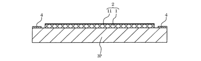
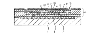
以下、本発明にかかる配線基板の製造方法の一実施形態について、図面を参照して詳細に説明する。図1〜図11は、本実施形態にかかる配線基板の製造方法を示す工程毎の図である。より詳細には、これらの図面のうち、図1は、支持基板3用のプリプレグ3Pおよび支持フィルム付き金属箔2ならびに金属枠4を準備する工程を示す概略断面図である。図2は、支持基板3用のプリプレグ3P上に支持フィルム付き金属箔2および金属枠4を載置した状態を示す概略断面図である。図3(a)は、支持基板3の主面上に支持フィルム付き金属箔2および金属枠4を積層した状態を示す概略断面図であり、図3(b)は、その状態を示す概略斜視図である。図4(a)は、支持フィルム付き金属箔2上およびその周辺上に第一の絶縁層21を積層した状態を示す概略断面図であり、図4(b)は、第一の絶縁層21に形成した切欠き部30を示す平面図である。図5は、第1の絶縁層21上に第2の導体層12を形成した状態を示す概略断面図である。図6は、第1の絶縁層21および第2の導体層12の上に層間絶縁用の第2〜第4の絶縁層22〜24と配線導体用の第3〜第5の導体層13〜15とを順次交互に形成し、さらにその上にソルダーレジスト用の第5の絶縁層25を形成して配線基板用の積層体10を形成した状態を示す概略断面図である。図7は、積層体10、支持フィルム2および支持基板3の中央部を切り出す工程を示す概略断面図である。図8は、切り出した積層体10、支持フィルム2および支持基板3の中央部を示す概略断面図である。図9は、切り出した積層体10を支持フィルム1から分離する工程を示す概略断面図である。図10は、第1の導体層11をエッチングして第一の絶縁層21の表面に配線導体を形成する工程を示す概略断面図である。図11は、エッチングされた金属箔11および第1の絶縁層21の表面にソルダーレジスト用の第6の絶縁層26を形成する工程を示す概略断面図である。
Hereinafter, an embodiment of a method for manufacturing a wiring board according to the present invention will be described in detail with reference to the drawings. FIGS. 1-11 is a figure for every process which shows the manufacturing method of the wiring board concerning this embodiment. More specifically, among these drawings, FIG. 1 is a schematic cross-sectional view showing a process of preparing the
まず、図1に示すように、支持フィルム付き金属箔2と、支持基板3用のプリプレグ3Pと、金属枠4とを準備する。支持フィルム付き金属箔2は、支持フィルム1上に金属箔11が粘着層(不図示)を介して保持されたものである。
First, as shown in FIG. 1, the
支持フィルム1は、厚みが10〜100μm程度であり、金属箔11に破れや皺が発生するのを有効に防止するとともに、金属箔11の取扱いを容易とするためのものである。支持フィルム1としては、例えばポリエステル樹脂等の耐熱性樹脂から成るのが好ましい。具体例としては、ポリエチレンテレフタレート(PET)フィルム等が挙げられる。
The
金属箔11は、配線基板の製造における起点となる導体層を提供するためのものである。金属箔11としては、例えば銅(銅箔)等の良導電性金属から成るのが好ましい。金属箔11の厚みとしては、例えば1〜35μm程度が挙げられる。これにより、該金属箔11をエッチング除去する際には、短時間でエッチング除去することができる。また、このような厚みの金属箔11は、全てエッチング除去する必要はなく、所定パターンにエッチングし配線導体の一部(外部接続用のパッド)として好適に利用することができる。これに対し、金属箔11の厚みが1μmより薄いと、金属箔11の強度が低下し、この金属箔11上に絶縁層と導体層とを交互に複数積層する際の作業性が低下するおそれがあり、35μmより厚いと、必要以上に厚くなりすぎるとともに、エッチング除去する際に要する時間が長くなるので好ましくない。
The
前記粘着層としては、配線基板の製造中にかかる熱負荷に耐え得る上で、例えばシリコーン樹脂系、アクリル樹脂系、ポリオルガノシロキサン樹脂系等の耐熱性粘着材から成るのが好ましい。また、前記粘着剤層は、後述する配線基板用の積層体10を破損することなく支持フィルム1から分離する上で、厚みが0.01〜1.0μm程度であり、粘着力が1〜10N/m程度であるのが好ましい。
The pressure-sensitive adhesive layer is preferably made of a heat-resistant pressure-sensitive adhesive material such as a silicone resin-based resin, an acrylic resin-based resin, or a polyorganosiloxane resin-based material in order to withstand the heat load applied during the production of the wiring board. The pressure-sensitive adhesive layer has a thickness of about 0.01 to 1.0 μm and an adhesive strength of 1 to 10 N in order to separate from the
プリプレグ3Pは、後述する配線基板用の積層体10を製造する際に該積層体10を必要な平坦度を維持して支持するための支持基板3となるものであり、その主面に支持フィルム付き金属箔2や金属枠4を載置し、それらを上下から加圧しながら加熱することによりプリプレグ3Pに支持フィルム付き金属箔2や金属枠4が積層され、その状態で熱硬化する。プリプレグ3Pは、通常、厚み0.2〜2.0mm程度、1辺の長さ300〜1000mm程度の略四角形の平板で構成されるが、これに限定されるものではない。プリプレグ3Pとしては、例えばガラス繊維等の耐熱性繊維から成る織布にエポキシ樹脂等の熱硬化性樹脂を含浸させて半硬化状態のシート状としたもの等が挙げられる。
The
金属枠4は、後述する配線基板用の積層体10を製造する際に、めっき用の電荷供給電極として使用するためのものであり、厚みが12〜35μm程度である。金属枠4としては、例えば銅等の良導電性金属から成るのが好ましい。
The
上記のような各材料を準備した後、図2に示すように、プリプレグ3Pの主面中央部上に支持フィルム付き金属箔2を、支持フィルム1がプリプレグ3Pの主面と対向するようにして配置するとともに、プリプレグ3Pの主面外周部上に金属枠4を配置する。そして、これらを上下から0.5〜9MPaの圧力でプレスしながら130〜200℃の温度で30分間〜120分間程度加熱することにより、図3(a),(b)に示すように、プリプレグ3Pが熱硬化して形成された支持基板3の主面に、支持フィルム付き金属箔2を金属箔11の上面が露出するようにして積層するとともに、支持基板3の主面の外周部に、金属箔11を取り囲む金属枠4をその上面が露出するようにして積層する。
After preparing each material as described above, as shown in FIG. 2, the
積層後は、露出した金属箔11の上面と、露出した金属枠4の上面と、金属箔11と金属枠4との間から露出した支持基板3の主面とが、実質的に同じ高さになる。これにより、後述する配線基板用の積層体10を平坦性に優れる面で支持することができるので、加工に伴う反りや、うねりの発生を抑制しつつ、積層体10を得ることができる。なお、露出した金属箔11の上面、金属枠4の上面、および金属箔11と金属枠4との間から露出した支持基板3の主面とは、完全に同一高さである必要はなく、これらの間に5μm以下の高低差があってもよい。
After the lamination, the upper surface of the exposed
次に、図4(a)に示すように、露出した金属箔(第1の導体層)11の上面と、露出した金属枠4の上面と、金属箔11と金属枠4との間から露出した支持基板3の主面上とに層間絶縁用の第1の絶縁層21を積層する。第1の絶縁層21には、図4(b)に示すように、金属枠4の外周側の一部を露出させる切欠き部30が、第1の絶縁層21の周方向における2箇所で互いに向き合うように形成されている。第1の絶縁層21は、例えばエポキシ樹脂やビスマレイミドトリアジン樹脂等の熱硬化性樹脂にシリカやタルク等の無機絶縁性フィラーを分散させた電気絶縁材料から成る。あるいは、ガラスクロスに熱硬化性樹脂を含浸させた電気絶縁材料であってもよい。
Next, as shown in FIG. 4A, the exposed upper surface of the exposed metal foil (first conductor layer) 11, the exposed upper surface of the
このような第1の絶縁層21は、例えばエポキシ樹脂やビスマレイミドトリアジン樹脂等の熱硬化性樹脂の未硬化物に無機絶縁性フィラーを分散させた混合物をペースト状としたものを、露出した金属箔11の上面、露出した金属枠4の上面(切欠き部30に対応する位置を除く)、および金属箔11と金属枠4との間から露出した支持基板3の主面上に塗布した後に熱硬化させることによって形成される。また、これに限定されるものではなく、例えば前記混合物をフィルム状としたものやガラスクロスに未硬化の熱硬化性樹脂を含浸させたプリプレグを、露出した金属箔11の上面、露出した金属枠4の上面(切欠き部30に対応する位置を除く)、および金属箔11と金属枠4との間から露出した支持基板3の主面上に張着した後に熱硬化させることにより形成してもよい。
Such a first insulating
第1の絶縁層21には、金属箔11の一部を露出させるビア用の開口部Vを形成する。開口部Vは、例えばレーザ加工により形成する。あるいは第1の樹脂層21用の混合物に感光性を持たせておき、それにフォトリソグラフィー技術を採用して露光・現像処理を施すこと等により形成することもできるが、これらに限定されるものではない。
In the first insulating
次に、図5に示すように、第1の絶縁層21の表面および開口部V内に配線導体用の第2の導体層12を所定のパターンに形成する。第2の導体層12は、例えば無電解銅めっき膜および電解銅めっき膜等から成り、周知のセミアディティブ法によって形成するのが好ましい。セミアディティブ法は微細配線化に優れるので、薄型で高密度な配線基板を効率よく製造するのに好適である。具体的には、まず、第1の絶縁層21の表面を必要に応じて粗化し、次にその表面に無電解銅めっき膜を0.1〜2.0μm程度の厚みに被着させる。このとき、切欠き部30から露出した金属枠4の表面にも無電解銅めっき膜を0.1〜2.0μm程度の厚みに被着させる。
Next, as shown in FIG. 5, the
次に、第1の絶縁層21の表面に被着した無電解銅めっき膜の表面に、第2の導体層12に対応した開口部を有するめっきレジスト層を形成する。このめっきレジスト層は、感光性の樹脂フィルムを前記無電解銅めっき膜上に張着するとともに、その樹脂フィルムにフォトリソグラフィー技術を採用して露光・現像処理を施すことにより前記開口部を有するように形成される。次に、めっきレジスト層の開口部内に露出する前記無電解銅めっき膜上に電解銅めっき膜を5〜30μm程度の厚みに被着させる。このとき、切欠き部30から露出した金属枠4を電解めっき用の電荷を供給するための電荷供給電極として使用することができる。これにより、金属枠4と電解めっき装置の陰極とを電気的に確実に接続することができる。これに対し、金属枠4がない場合には、極めて薄い無電解銅めっき膜に電解めっき装置の端子を接続することになり、無電解銅めっき膜が擦れたり破れたりして安定した給電が困難になる。
次に、めっきレジスト層を剥離した後、前記無電解銅めっき膜および電解銅めっき膜の露出部を電解銅めっき膜間の無電解銅めっき膜が消失するまで全体的にエッチングして第2の導体層12を形成する。
Next, a plating resist layer having an opening corresponding to the
Next, after peeling off the plating resist layer, the exposed portion of the electroless copper plating film and the electrolytic copper plating film is etched entirely until the electroless copper plating film between the electrolytic copper plating films disappears to form a second The
このようにして第2の導体層12を形成した後、図6に示すように、第1の絶縁層21および第2の導体層12の上に層間絶縁用の第2〜第4の絶縁層22〜24と、配線導体用の第3〜第5の導体層13〜15とを順次交互に形成し、さらにその上にソルダーレジスト用の第5の絶縁層25を形成して配線基板用の積層体10を形成する。
After the
層間絶縁用の第2〜第4の絶縁層22〜24は、第1の絶縁層21と同様の電気絶縁材料から成り、第1の絶縁層21と同様の方法により形成することができる。また、配線導体用の第3〜第5の導体層13〜15は、第2の導体層12と同様の無電解銅めっき膜および電解銅めっき膜から成り、第2の導体層12と同様のセミアディティブ法にて形成するのが好ましい。さらに、ソルダーレジスト用の第5の絶縁層25は、例えばアクリル変性エポキシ樹脂にシリカやタルク等の無機物粉末フィラーを30〜70質量%程度分散させた電気絶縁材料から成り、アクリル変性エポキシ樹脂等の感光性樹脂と光重合開始剤等とから成る混合物にシリカやタルク等の無機絶縁性フィラーを含有させた感光性樹脂ペーストを、第4の絶縁層24および第5の導体層15の上にスクリーン印刷やロールコート法等により10〜30μm程度の厚みに塗布し、しかる後、フォトリソグラフィー技術を採用して所定のパターンに露光・現像した後、それを紫外線硬化および熱硬化させることにより形成するのが好ましい。
The second to fourth insulating
次に、図7に示すように、金属枠4の内側領域に位置する積層体10および支持基板3を切断する。かかる切断を効率よく行う上で、積層体10および支持フィルム1および支持基板3を、金属箔11の外周から10〜30mm内側に位置する部分で切断して、図8に示すように、積層体10の中央部を支持フィルム1および支持基板3とともに切り出すのが好ましい。前記切断の方法は、本発明の効果を妨げない範囲内で任意であり、例えばダイシングやルーター装置等を用いて切断すればよい。
Next, as shown in FIG. 7, the laminate 10 and the
次に、図9に示すように、切り出した積層体10を支持フィルム1から分離する。この分離の際には、支持フィルム1上に金属箔11が図示しない粘着層を介して保持されているだけなので、支持フィルム1と金属箔11間を引き剥がすだけで積層体10を破損することなく、簡単に分離することができる。
Next, as shown in FIG. 9, the
次に、図10に示すように、金属箔(第1の導体層)11を所定のパターンにエッチングするエッチング工程を施して第1の絶縁層21の表面に配線導体(外部接続用のパッド)を形成する。金属箔11を所定のパターンにエッチングするには、例えば配線導体に対応する形状のエッチングレジスト層を金属箔11の表面に形成するとともに、そのエッチングレジスト層から露出した金属箔11をエッチング除去すればよい。なお、前記エッチングレジスト層は、感光性の樹脂フィルムを金属箔11上に張着するとともに、その樹脂フィルムにフォトリソグラフィー技術を採用して露光・現像処理を施すことにより前記配線導体に対応する形状に形成され、金属箔11をエッチングした後に剥離する。
Next, as shown in FIG. 10, an etching process for etching the metal foil (first conductor layer) 11 into a predetermined pattern is performed to form a wiring conductor (pad for external connection) on the surface of the first insulating
最後に、図11に示すように、エッチングされた金属箔11および第1の絶縁層21の表面にソルダーレジスト用の第6の絶縁層26を形成して本実施形態にかかる配線基板20を得る。このように本実施形態によれば、支持基板3上に直接積層体10を形成するのではなく、まず支持基板3の主面に、支持フィルム付き金属箔2を金属箔11の上面が露出するようにして積層し、ついで前記金属箔11上に絶縁層と導体層とを交互に複数積層して積層体10を得るので、支持フィルム付き金属箔2の支持フィルム1を積層体10と支持基板3とを分離する際にその分離を容易とするための境界層として機能させることができ、その結果、積層体10を支持基板3から短時間の間に容易に剥離することができる。しかも、金属箔11は、所定パターンにエッチングして配線導体の一部として利用することができる。したがって、本実施形態によれば、薄型で高密度な配線基板20を効率よく製造することが可能となる。なお、ソルダーレジスト用の第6の絶縁層26は、第5の絶縁層25と同様の材料から成り、第5の絶縁層25と同様の方法によって形成される。
Finally, as shown in FIG. 11, a sixth insulating
前記した一実施形態では、1枚の支持基板3上に配線基板用の積層体10を形成した場合について説明したが、本発明にかかる他の実施形態として、例えば2枚の支持基板3を背中合わせに重ね合わせ、それぞれの支持基板3の外側主面に配線基板用の積層体10を同時に形成してもよい。図12は、本実施形態にかかる配線基板の製造方法を示す概略断面図であり、上記で説明した図1に相当する図である。なお、図12においては、前述した図1〜11と同一の構成部分には同一の符号を付して説明は省略する。
In the above-described embodiment, the case where the
図12に示すように、本実施形態にかかる積層体10を形成する工程は、まず、支持フィルム付き金属箔2と、支持基板3用のプリプレグ3Pと、金属枠体4と、分離フィルム5とをそれぞれ2枚ずつ準備する。分離フィルム5は、各支持基板3上に積層体10を形成した後、2枚の支持基板3同士を容易に分離させるための境界層として機能するものである。分離フィルム5は、例えば銅箔等の金属箔や、ポリエチレンテレフタレート(PET)フィルム等の耐熱フィルム等から成るのが好ましい。分離フィルム5の厚さとしては、例えば1〜35μm程度であるのが好ましい。
As shown in FIG. 12, the process of forming the
このような分離フィルム5を含む各材料を準備した後、図13〜図18に示すようにして積層体10を得、この積層体10を用いて配線基板20を得る。すなわち、図13に示すように、2枚のプリプレグ3Pにおける中央部の間に分離フィルム5を2枚重ねて挟持するとともに、各プリプレグ3Pの外側の主面中央部上に支持フィルム付き金属箔2と、前記外側主面の外周部に金属枠4とをそれぞれ配置する。次に、これらを上下からプレスしながら加熱することにより、図14に示すように、プリプレグ3Pが熱硬化して形成一体化された2枚の支持基板3の間に、2枚の分離フィルム5を互いに重なった状態で封入するとともに、各支持基板3の外側主面に支持フィルム付き金属箔2および金属枠4を積層する。このとき、2枚の分離フィルム5は、互いに接着されておらず、支持基板3とのみ接着している。
After preparing each material including such a
次に、図15に示すように、2枚の支持基板3の各外側主面上に配線基板用の積層体10をそれぞれ同時に形成する。なお、各積層体10の形成は、前記一実施形態において図4〜図6を基にして説明した工程と同様にして行なう。
Next, as shown in FIG. 15, the
次に、図16に示すように、積層体10、支持フィルム1および支持基板3ならびに分離フィルム5を、金属箔11の外周から10〜30mm内側に位置する部分で切断することにより、図17に示すように、各積層体10の中央部を支持フィルム1および支持基板3ならびに剥離フィルム5とともに切り出す。このとき、剥離フィルム5同士は接着されていないので、両者は容易に分離される。
Next, as shown in FIG. 16, the laminate 10, the
次に、図18に示すように、切り出した各積層体10を前記一実施形態の場合と同様にして支持フィルム1から分離する。これにより、2つの積層体10を得ることができるので、前記一実施形態よりも積層体10を形成する際の効率を約2倍に高めることができる。その後、分離した各積層体10に、前記一実施形態において図10,図11を基に説明した工程を施すことにより、2つの配線基板20を得る。したがって、本実施形態によれば、薄型で高密度な配線基板20を更に効率よく製造することが可能となる。
Next, as shown in FIG. 18, each cut-out
本発明にかかる更に他の実施形態として、2枚の支持基板3を、これら間に両者の分離を容易とするための別の分離用基板を介在させて重ね合わせ、それぞれの支持基板3の外側主面に配線基板用の積層体10を同時に形成してもよい。図19は、本実施形態にかかる配線基板の製造方法を示す概略断面図であり、上記で説明した図1,図12に相当する図である。なお、図19においては、前述した図1〜18と同一の構成部分には同一の符号を付して説明は省略する。
As still another embodiment according to the present invention, two
図19に示すように、本実施形態にかかる積層体10を形成する工程は、まず、支持フィルム付き金属箔2と、支持基板3用のプリプレグ3Pと、金属枠体4と、分離フィルム5とをそれぞれ2枚ずつ準備するとともに、分離用基板6を1枚準備する。分離用基板6は、各支持基板3上に積層体10を形成した後、2枚の支持基板3同士を容易に分離させるための境界層として機能するものである。分離用基板6は、例えば厚みが50〜400μm程度のガラス−エポキシ板7の両面に、厚みが12〜35μm程度の銅箔8を積層した両面銅張板等から成る。
As shown in FIG. 19, the step of forming the
このような分離用基板6を含む各材料を準備した後、図20〜図24に示すようにして積層体10を得、この積層体10を用いて配線基板20を得る。すなわち、図20に示すように、2枚のプリプレグ3P間に分離用基板6を挟むとともに、分離用基板6とプリプレグ3Pとの間の中央部に分離フィルム5を配置し、さらに各プリプレグ3Pの外側の主面中央部上に支持フィルム付き金属箔2と、前記外側主面の外周部に金属枠4とをそれぞれ配置する。
After preparing each material including such a
次に、これらを上下からプレスしながら加熱することにより、図21に示すように、プリプレグ3Pが熱硬化した2枚の支持基板3の間に分離用基板6を積層一体化するとともに、分離用基板6と支持基板3との間に分離フィルム5を封入し、さらに各支持基板3の外側主面に支持フィルム付き金属箔2および金属枠4を積層する。このとき、分離用基板6と分離フィルム5とは互いに接着されておらず、支持基板3とのみ接着している。
Next, by heating them while pressing them from above and below, as shown in FIG. 21, the
次に、図22に示すように、2枚の支持基板3の各外側主面上に配線基板用の積層体10をそれぞれ同時に形成する。なお、各積層体10の形成は、前記一実施形態において図4〜図6を基にして説明した工程と同様にして行なう。
Next, as shown in FIG. 22, wiring board laminates 10 are simultaneously formed on the respective outer principal surfaces of the two
次に、図23に示すように、積層体10、支持フィルム1、支持基板3および分離フィルム5ならびに分離用基板6を、金属箔11の外周から10〜30mm内側に位置する部分で切断することにより、図24に示すように、各積層体10の中央部を支持フィルム1および支持基板3ならびに剥離フィルム5とともに切り出す。このとき、分離フィルム5と分離用基板6とは接着されていないので、両者は容易に分離される。
Next, as shown in FIG. 23, the laminate 10, the
次に、前記他の実施形態において図18を基に説明したのと同様にして、切り出した積層体10を支持フィルム1から分離する。これにより、2つの積層体10を得ることができるので、前記一実施形態よりも積層体10を形成する効率を約2倍に高めることができる。その後、分離した各積層体10に、前記一実施形態において図10,図11を基に説明した工程を施すことにより、2つの配線基板20を得る。したがって、本実施形態によれば、薄型で高密度な配線基板20を更に効率よく製造することが可能となる。
Next, the
かくして本発明の配線基板の製造方法によれば、薄型で高密度な配線基板を効率よく製造することができる。なお、本発明は、上述の実施の形態例に限定されるものではなく、本発明の要旨を逸脱しない範囲であれば、種々の変更が可能であることは言うまでもない。例えば、前記したいくつかの実施形態では、金属箔11は、所定パターンにエッチングして配線導体の一部として利用する場合について説明したが、本発明はこれに限定されるものではなく、図25に示すように、必要に応じて該金属箔11を全てエッチング除去してもよい。この場合には、絶縁層21のビア内に露出する導体層12が外部接続用のパッドとなる。
Thus, according to the method for manufacturing a wiring board of the present invention, a thin and high-density wiring board can be efficiently manufactured. It should be noted that the present invention is not limited to the above-described embodiment, and it goes without saying that various modifications can be made without departing from the gist of the present invention. For example, in the above-described embodiments, the case where the
さらには、図26に示すように、金属箔11の上に、例えば銅等から成る外部接続用のパッドPをセミアディティブ法やフルアディティブ法等により形成し、その上に絶縁層21〜25と導体層12〜15とを交互に積層し、パッドPを構成要素として含む配線基板用の積層体10を形成し、これを切り出して支持フィルム1より分離した後、図27に示すように、金属箔11を全てエッチング除去してパッドPを露出させてもよい。
Furthermore, as shown in FIG. 26, a pad P for external connection made of, for example, copper or the like is formed on the
金属枠4を電荷供給電極として使用する上で、絶縁層21に切欠き部30を形成した場合について説明したが、切欠き部30に代えて、例えば金属枠4の全ての外周側が枠状に露出するように絶縁層21を積層してもよい。
In the case where the
1 支持フィルム
2 支持フィルム付き金属箔
3P プリプレグ
3 支持基板
4 金属枠
5 分離フィルム
6 分離用基板
10 配線基板用の積層体
11 金属箔
12〜15 導体層
21〜26 絶縁層
20 配線基板
30 切欠き部
DESCRIPTION OF
Claims (4)
この外部接続用のパッドが形成された金属箔上に絶縁層と導体層とを交互に複数積層して、前記金属箔と前記絶縁層と前記導体層と、さらに前記外部接続用のパッドとから成る配線基板用の積層体を形成する工程と、
この積層体を前記支持フィルムから分離する工程と、
分離した前記積層体において、前記金属箔の全てをエッチングして除去し、前記外部接続用のパッドを露出させる工程とを含む請求項1記載の配線基板の製造方法。 Including a step of forming a pad for external connection on the metal foil before the step of forming the laminate,
A plurality of insulating layers and conductor layers are alternately laminated on the metal foil on which the pads for external connection are formed, and the metal foil, the insulating layers, the conductor layers, and the pads for external connection. Forming a laminate for a wiring board comprising:
Separating the laminate from the support film;
In separate the laminate, all of the metal foil is removed by etching, method of manufacturing a wiring board according to claim 1 further comprising the step of exposing the pads for the external connection.
Priority Applications (1)
| Application Number | Priority Date | Filing Date | Title |
|---|---|---|---|
| JP2007199651A JP4994988B2 (en) | 2007-07-31 | 2007-07-31 | Wiring board manufacturing method |
Applications Claiming Priority (1)
| Application Number | Priority Date | Filing Date | Title |
|---|---|---|---|
| JP2007199651A JP4994988B2 (en) | 2007-07-31 | 2007-07-31 | Wiring board manufacturing method |
Publications (2)
| Publication Number | Publication Date |
|---|---|
| JP2009038134A JP2009038134A (en) | 2009-02-19 |
| JP4994988B2 true JP4994988B2 (en) | 2012-08-08 |
Family
ID=40439783
Family Applications (1)
| Application Number | Title | Priority Date | Filing Date |
|---|---|---|---|
| JP2007199651A Active JP4994988B2 (en) | 2007-07-31 | 2007-07-31 | Wiring board manufacturing method |
Country Status (1)
| Country | Link |
|---|---|
| JP (1) | JP4994988B2 (en) |
Families Citing this family (9)
| Publication number | Priority date | Publication date | Assignee | Title |
|---|---|---|---|---|
| JP5177855B2 (en) * | 2008-02-29 | 2013-04-10 | 京セラSlcテクノロジー株式会社 | Wiring board manufacturing method |
| KR101097741B1 (en) | 2009-09-14 | 2011-12-22 | 아페리오(주) | Method of forming a die attachment pad and a solder ball pad on each side of a single conducting layer and package substrate manufactured thereof |
| JP5409519B2 (en) * | 2010-05-31 | 2014-02-05 | 京セラSlcテクノロジー株式会社 | Wiring board and manufacturing method thereof |
| JP5606268B2 (en) | 2010-10-27 | 2014-10-15 | 日本特殊陶業株式会社 | Manufacturing method of multilayer wiring board |
| KR101216926B1 (en) * | 2011-07-12 | 2012-12-28 | 삼성전기주식회사 | Carrier member and method for manufacturing the same and method for manufacturing of printed circuit board using the same |
| JP2013115316A (en) * | 2011-11-30 | 2013-06-10 | Shin Etsu Polymer Co Ltd | Manufacturing method of wiring board |
| TWI474450B (en) * | 2013-09-27 | 2015-02-21 | 旭德科技股份有限公司 | Package carrier and manufacturing method thereof |
| TWI474449B (en) * | 2013-09-27 | 2015-02-21 | 旭德科技股份有限公司 | Package carrier board and manufacturing method thereof |
| EP3618587A4 (en) * | 2017-04-27 | 2020-04-08 | Mitsubishi Gas Chemical Company, Inc. | SUPPORT AND METHOD FOR MANUFACTURING A SEMICONDUCTOR ELEMENT MOUNTING SUBSTRATE USING THE SAME |
Family Cites Families (9)
| Publication number | Priority date | Publication date | Assignee | Title |
|---|---|---|---|---|
| JP2004247391A (en) * | 2003-02-12 | 2004-09-02 | Toray Ind Inc | Circuit board manufacturing method |
| JP2004281943A (en) * | 2003-03-18 | 2004-10-07 | Ngk Spark Plug Co Ltd | Manufacturing method of wiring board |
| JP2004319981A (en) * | 2003-03-28 | 2004-11-11 | Toray Ind Inc | Transfer sheet for wiring board formation |
| JP4549695B2 (en) * | 2003-08-08 | 2010-09-22 | 日本特殊陶業株式会社 | Wiring board manufacturing method |
| JP2005079108A (en) * | 2003-08-29 | 2005-03-24 | Ngk Spark Plug Co Ltd | Wiring board manufacturing method |
| JP4547164B2 (en) * | 2004-02-27 | 2010-09-22 | 日本特殊陶業株式会社 | Wiring board manufacturing method |
| JP4445778B2 (en) * | 2004-02-27 | 2010-04-07 | 日本特殊陶業株式会社 | Wiring board manufacturing method |
| JP4445777B2 (en) * | 2004-02-27 | 2010-04-07 | 日本特殊陶業株式会社 | Wiring board and method for manufacturing wiring board |
| JP2007067382A (en) * | 2005-08-03 | 2007-03-15 | Toray Ind Inc | Wiring board forming carrier, wiring board forming base material, and wiring board manufacturing method using them |
-
2007
- 2007-07-31 JP JP2007199651A patent/JP4994988B2/en active Active
Also Published As
| Publication number | Publication date |
|---|---|
| JP2009038134A (en) | 2009-02-19 |
Similar Documents
| Publication | Publication Date | Title |
|---|---|---|
| JP4994988B2 (en) | Wiring board manufacturing method | |
| JP4874305B2 (en) | Circuit board with built-in electric / electronic components and manufacturing method thereof | |
| JP2006203155A (en) | Method for manufacturing rigid flexible printed circuit board | |
| TW201438537A (en) | Wiring substrate manufacturing method | |
| JP2013187255A (en) | Wiring board manufacturing method | |
| JP2015109392A (en) | Wiring board manufacturing method | |
| JP5177855B2 (en) | Wiring board manufacturing method | |
| JP2017011251A (en) | Wiring board and manufacturing method thereof | |
| JP5047906B2 (en) | Wiring board manufacturing method | |
| CN104780723A (en) | Method for manufacturing wiring board | |
| KR101044105B1 (en) | Substrate manufacturing method for preventing warpage | |
| TWI864015B (en) | Method for manufacturing circuit board | |
| JP2013123035A (en) | Manufacturing method for multilayer wiring board | |
| JPWO2014125567A1 (en) | Component built-in substrate and manufacturing method thereof | |
| KR101055571B1 (en) | Carrier member for substrate manufacturing and method for manufacturing substrate using same | |
| JP5057339B2 (en) | Wiring board manufacturing method | |
| JP4161604B2 (en) | Printed wiring board and manufacturing method thereof | |
| JP2020004930A (en) | Printed-wiring board | |
| JP5483921B2 (en) | Method for manufacturing printed circuit board | |
| JP5955050B2 (en) | Wiring board manufacturing method | |
| KR101044117B1 (en) | Manufacturing method of printed circuit board | |
| JP4503698B2 (en) | Wiring board manufacturing method | |
| JP2009194312A (en) | Wiring substrate and method for manufacturing the same | |
| JP2012209322A (en) | Method of manufacturing wiring board | |
| JP2015144150A (en) | Manufacturing method of wiring board |
Legal Events
| Date | Code | Title | Description |
|---|---|---|---|
| A621 | Written request for application examination |
Free format text: JAPANESE INTERMEDIATE CODE: A621 Effective date: 20100416 |
|
| A977 | Report on retrieval |
Free format text: JAPANESE INTERMEDIATE CODE: A971007 Effective date: 20111125 |
|
| A131 | Notification of reasons for refusal |
Free format text: JAPANESE INTERMEDIATE CODE: A131 Effective date: 20111129 |
|
| A521 | Written amendment |
Free format text: JAPANESE INTERMEDIATE CODE: A523 Effective date: 20120127 |
|
| TRDD | Decision of grant or rejection written | ||
| A01 | Written decision to grant a patent or to grant a registration (utility model) |
Free format text: JAPANESE INTERMEDIATE CODE: A01 Effective date: 20120501 |
|
| A01 | Written decision to grant a patent or to grant a registration (utility model) |
Free format text: JAPANESE INTERMEDIATE CODE: A01 |
|
| A61 | First payment of annual fees (during grant procedure) |
Free format text: JAPANESE INTERMEDIATE CODE: A61 Effective date: 20120509 |
|
| FPAY | Renewal fee payment (event date is renewal date of database) |
Free format text: PAYMENT UNTIL: 20150518 Year of fee payment: 3 |
|
| R150 | Certificate of patent or registration of utility model |
Ref document number: 4994988 Country of ref document: JP Free format text: JAPANESE INTERMEDIATE CODE: R150 Free format text: JAPANESE INTERMEDIATE CODE: R150 |
|
| R250 | Receipt of annual fees |
Free format text: JAPANESE INTERMEDIATE CODE: R250 |
|
| S531 | Written request for registration of change of domicile |
Free format text: JAPANESE INTERMEDIATE CODE: R313531 |
|
| S533 | Written request for registration of change of name |
Free format text: JAPANESE INTERMEDIATE CODE: R313533 |
|
| R350 | Written notification of registration of transfer |
Free format text: JAPANESE INTERMEDIATE CODE: R350 |
|
| R250 | Receipt of annual fees |
Free format text: JAPANESE INTERMEDIATE CODE: R250 |
|
| S111 | Request for change of ownership or part of ownership |
Free format text: JAPANESE INTERMEDIATE CODE: R313111 |
|
| R350 | Written notification of registration of transfer |
Free format text: JAPANESE INTERMEDIATE CODE: R350 |