JP4921058B2 - Imaging apparatus and control method thereof - Google Patents
Imaging apparatus and control method thereof Download PDFInfo
- Publication number
- JP4921058B2 JP4921058B2 JP2006194755A JP2006194755A JP4921058B2 JP 4921058 B2 JP4921058 B2 JP 4921058B2 JP 2006194755 A JP2006194755 A JP 2006194755A JP 2006194755 A JP2006194755 A JP 2006194755A JP 4921058 B2 JP4921058 B2 JP 4921058B2
- Authority
- JP
- Japan
- Prior art keywords
- dark current
- image
- dark
- amount
- image sensor
- Prior art date
- Legal status (The legal status is an assumption and is not a legal conclusion. Google has not performed a legal analysis and makes no representation as to the accuracy of the status listed.)
- Expired - Fee Related
Links
Images






Classifications
-
- H—ELECTRICITY
- H04—ELECTRIC COMMUNICATION TECHNIQUE
- H04N—PICTORIAL COMMUNICATION, e.g. TELEVISION
- H04N25/00—Circuitry of solid-state image sensors [SSIS]; Control thereof
- H04N25/60—Noise processing, e.g. detecting, correcting, reducing or removing noise
- H04N25/63—Noise processing, e.g. detecting, correcting, reducing or removing noise applied to dark current
-
- H—ELECTRICITY
- H04—ELECTRIC COMMUNICATION TECHNIQUE
- H04N—PICTORIAL COMMUNICATION, e.g. TELEVISION
- H04N25/00—Circuitry of solid-state image sensors [SSIS]; Control thereof
- H04N25/60—Noise processing, e.g. detecting, correcting, reducing or removing noise
- H04N25/63—Noise processing, e.g. detecting, correcting, reducing or removing noise applied to dark current
- H04N25/633—Noise processing, e.g. detecting, correcting, reducing or removing noise applied to dark current by using optical black pixels
-
- H—ELECTRICITY
- H04—ELECTRIC COMMUNICATION TECHNIQUE
- H04N—PICTORIAL COMMUNICATION, e.g. TELEVISION
- H04N25/00—Circuitry of solid-state image sensors [SSIS]; Control thereof
- H04N25/60—Noise processing, e.g. detecting, correcting, reducing or removing noise
- H04N25/68—Noise processing, e.g. detecting, correcting, reducing or removing noise applied to defects
Landscapes
- Engineering & Computer Science (AREA)
- Multimedia (AREA)
- Signal Processing (AREA)
- Transforming Light Signals Into Electric Signals (AREA)
- Solid State Image Pick-Up Elements (AREA)
- Studio Devices (AREA)
Description
本発明は、撮像素子を備えた撮像装置及びその制御方法に関する。 The present invention relates to an imaging apparatus including an imaging element and a control method thereof.
撮像素子を用いて長時間露光を行う場合、高ISO感度での撮影を行う場合、及び高温度下で撮影を行う場合等には撮像素子が暗電流を生じることが知られている。暗電流の発生は、固体撮像素子が光エネルギーを電気信号に変換するだけでなく、熱エネルギーをも電気信号に変換する性質を有することによる。そして、暗電流は温度依存性が高く、温度が8〜10℃上昇すると、その出力はおよそ2倍になることが知られている。固体撮像素子では、暗電流が画質に悪影響を与えるため、その成分を小さくするよう、製造上数々の工夫がなされている。 It is known that when an image sensor is used for long exposure, when imaging is performed at a high ISO sensitivity, and when imaging is performed at a high temperature, the imaging element generates a dark current. The dark current is generated because the solid-state imaging device has a property of not only converting light energy into an electric signal but also converting heat energy into an electric signal. And it is known that the dark current has a high temperature dependency, and when the temperature rises by 8 to 10 ° C., the output is approximately doubled. In the solid-state imaging device, since the dark current adversely affects the image quality, many devices have been devised in order to reduce the component.
撮像素子全体が置かれた環境による撮像素子全体の温度上昇だけでなく、撮像素子の一部の消費電流が大きい場合、例えば出力段アンプなどの消費電流が多い場合には、撮像素子の部分的な温度上昇が発生することがある。このような場合、その部分のみ暗電流が上昇し出力が大きくなることが見受けられる。例えば高ISO長秒時で夜景等を撮影した場合には、本来まったく明かりのない領域にマゼンタに近い色の明かりが見受けられたりする。 In addition to the temperature rise of the entire image sensor due to the environment where the entire image sensor is placed, if the current consumption of a part of the image sensor is large, for example, if the current consumption of the output stage amplifier is large, a partial image sensor Temperature rise may occur. In such a case, it can be seen that the dark current increases only in that portion and the output increases. For example, when a night scene or the like is photographed at a high ISO long time, a light of a color close to magenta may be seen in an originally originally unlit area.
そして、撮像素子の暗電流が大きくなると、暗電流に面内の分布ばらつきがある場合、面内の輝度、色バランスがおかしくなることがある。また、暗電流が全面で大きくなると、ダークレベルが上昇し、相対的に光信号のダイナミックレンジが減少してしまう。このように、暗電流の増加は画質に大きな影響を与えるという問題がある。 When the dark current of the image sensor increases, the in-plane brightness and color balance may be incorrect if the dark current has in-plane distribution variations. Further, when the dark current increases on the entire surface, the dark level increases, and the dynamic range of the optical signal relatively decreases. Thus, there is a problem that an increase in dark current has a large effect on image quality.
このような問題を解消するための処理として、暗電流の影響をキャンセルする長秒時のノイズリダクション処理(所謂、ダーク画像減算処理)が知られている。このノイズリダクション処理では、本画像の撮影後に、本画像撮影時とまったく同じ条件で撮像素子を遮光した状態で画像を撮影し(ダーク画像)、本画像からこのダーク画像を減算する。 As a process for solving such a problem, a long-second noise reduction process (so-called dark image subtraction process) for canceling the influence of dark current is known. In this noise reduction process, after the main image is captured, the image is captured (dark image) under the same conditions as when the main image is captured (dark image), and the dark image is subtracted from the main image.
しかしながら、ダーク画像減算処理には一般に次のような問題がある。第1に、正確に本画像撮影時の暗電流の影響をキャンセルするには、本画像撮影時と同条件でダーク画像を取得することが望ましい。そのため長秒時の露光を行った場合には、更にそれと同じ時間のダーク画像取得時間を要するため、操作性が極めて悪化する。第2に、本画像からダーク画像の減算処理を行うことで、本画像及びダーク画像の持つランダムノイズが本画像の√2倍となってしまい本質的に画質の低下が避けられない。 However, the dark image subtraction process generally has the following problems. First, in order to accurately cancel the influence of dark current at the time of photographing the main image, it is desirable to acquire a dark image under the same conditions as at the time of photographing the main image. Therefore, when exposure is performed for a long time, the dark image acquisition time of the same time is further required, so that the operability is extremely deteriorated. Second, by performing the subtraction process of the dark image from the main image, the random noise of the main image and the dark image becomes √2 times that of the main image, and the deterioration of the image quality is inevitable.
そこで、特許文献1に、不要な撮影条件であれば、可能な限りノイズリダクション処理を行わないように、本撮影時の暗電流成分を検出し、その値が所定以上のときだけノイズリダクション処理を行う方法が提案されている。 Therefore, Japanese Patent Application Laid-Open Publication No. 2004-228561 detects a dark current component at the time of actual photographing so that noise reduction processing is not performed as much as possible under unnecessary photographing conditions, and performs noise reduction processing only when the value is equal to or greater than a predetermined value. A way to do it has been proposed.
一方で、撮像素子の画素欠陥の一種に白キズとよばれるものが存在する。白キズは、その暗電流が他の画素に比較して異常に多く、温度又は露光時間等の要因によりその出力が非常に大きなものとなり画像となったときに白点として見えてしまう画素である。白キズの暗電流は、主に撮像素子の画素を構成するフォトダイオード部の結晶欠陥に起因する現象で露光時間、撮像素子の温度によって変化することが知られている。従って、高温度環境化、長秒露光時にその影響が多く見られ、撮像素子出力により多くのゲインを乗じられる高ISO感度条件下でもそのゲイン分だけ実際の画像としては影響が大きくなってしまう。 On the other hand, there is a so-called white flaw as a kind of pixel defect of an image sensor. White scratches are pixels whose dark current is abnormally large compared to other pixels, and their output becomes very large due to factors such as temperature or exposure time, and appear as white spots when an image is formed. . It is known that the dark current due to white scratches is a phenomenon mainly caused by crystal defects in the photodiode portion constituting the pixel of the image sensor, and changes depending on the exposure time and the temperature of the image sensor. Therefore, the influence is often seen in high temperature environment and long-second exposure, and the influence is increased as an actual image by the gain even under a high ISO sensitivity condition in which a lot of gain is multiplied by the image sensor output.
このような温度、露光時間に依存するタイプの白キズの特徴として、例えば同一温度下で露光時間とその出力のグラフを作成すると、分布上いくつかの異なる傾きをとることが知られている。 As a characteristic of the type of white scratch that depends on the temperature and the exposure time, for example, when a graph of the exposure time and its output is created at the same temperature, it is known that the distribution has several different slopes.
但し、ノイズリダクション処理を行うか否かの判断に際しては、次の2つの点を両立させる必要がある。第1に、ノイズリダクションの悪影響が生じないように、必要がないときにはノイズリダクションを行わない。第2に、自動判定を謳う以上、わずかでも暗電流の影響が見えるようであれば、直ちにノイズリダクション処理を行う。このため、非常に高精度に暗電流量を検出する必要がある。 However, in determining whether or not to perform noise reduction processing, it is necessary to make the following two points compatible. First, noise reduction is not performed when it is not necessary so as not to adversely affect noise reduction. Secondly, as long as automatic determination is required, if the influence of dark current can be seen even slightly, noise reduction processing is immediately performed. For this reason, it is necessary to detect the dark current amount with very high accuracy.
しかしながら、画像として影響が見えるかどうかという領域で正確に判断することはその精度からして非常に困難ある。特に高ISO、長秒時の撮影条件ではそもそも画像のランダムノイズ成分が大きく、このような条件下で正確な暗電流の絶対値を検出するにはランダムノイズ成分を除去した上で測定する必要がある。このため、ファームウェアで処理するにしても、撮像素子の光学的遮光領域画像の一部分を読み出しランダムノイズ対策を行った後に暗電流量の検出を行う必要がある。この結果、演算量としてもかなりのリソースと演算時間を要し、その精度も決して十分であるとはいえない。 However, it is very difficult to accurately determine whether or not the influence is visible as an image because of its accuracy. In particular, random noise components of an image are large in the first place under shooting conditions at high ISO and long seconds, and in order to detect an accurate absolute value of dark current under such conditions, it is necessary to measure after removing the random noise components. is there. For this reason, even when processing is performed by firmware, it is necessary to detect the amount of dark current after reading out a part of the optically shielded area image of the image sensor and taking measures against random noise. As a result, the amount of calculation requires considerable resources and calculation time, and its accuracy is never sufficient.
また、ダークレベルのクランプ動作を行うAFEを使用するシステムにおいては、そもそも暗電流成分が画像データに現れにくいので、測定そのものが困難である。更に、ダーククランプを行うAFEを使用するシステムにおいて、VOB部分の暗電流量を検出するためには、ダークレベルクランプを行う前のダーク出力を読み出す必要がある。これには、限られた面積のオプティカルブラック部の中でクランプ動作を開始するタイミングを遅くしなければならず、大きな暗電流量をアナログ的にクランプするためにはその引き込み時間も必要となるため、非常に厳しいものである。また、このような状況から、クランプ前の出力を読み出すことができる画素数にも限りがあり、この中からノイズの影響をのぞいて正確に暗電流量を求めることも非常に困難である。 In addition, in a system using AFE that performs a clamp operation at a dark level, since the dark current component hardly appears in the image data, the measurement itself is difficult. Furthermore, in a system using AFE that performs dark clamping, it is necessary to read out the dark output before performing dark level clamping in order to detect the dark current amount in the VOB portion. For this purpose, the timing for starting the clamping operation must be delayed in the optical black portion of a limited area, and in order to clamp a large amount of dark current in an analog manner, the pull-in time is also required. It ’s very tough. In addition, from such a situation, the number of pixels from which the output before clamping can be read out is limited, and it is very difficult to accurately determine the dark current amount from the influence of noise.
一方、白キズの出力は正常画素の暗電流成分よりも大きいので、ある微小な欠陥画素についてその位置情報が事前にわかっていれば、撮影時にこのような出力を示す画素出力をモニターすることで暗電流よりも大きなゲインの出力を得ることが可能となる。つまり、事前に正常画素の暗電流成分との傾きの差を検出しておくことで、より高精度に暗電流成分を判断することが可能となる。 On the other hand, since the output of white scratches is larger than the dark current component of normal pixels, if the positional information of a minute defective pixel is known in advance, the pixel output indicating such output can be monitored at the time of shooting. It becomes possible to obtain an output with a gain larger than that of the dark current. That is, by detecting a difference in inclination from the dark current component of the normal pixel in advance, the dark current component can be determined with higher accuracy.
しかしながら、このような処理を行うためには、カメラの製造工程で個体毎に欠陥画素のレベルの検出、アドレス検出該当アドレスをカメラに記憶させる工程が必要となる。また、もちろん白キズの出力の精度上複数個のアドレスを検出、記憶し、判断する必要があり、現実的には非常に困難である。 However, in order to perform such processing, it is necessary to detect the level of the defective pixel and store the address detection corresponding address in the camera for each individual in the camera manufacturing process. Of course, it is necessary to detect, store and judge a plurality of addresses for the accuracy of the output of white flaws, which is very difficult in practice.
本発明は、容易に暗電流の量を高い精度で求めることができる撮像装置及びその制御方法を提供することを目的とする。 An object of the present invention is to provide an imaging apparatus and a control method thereof that can easily determine the amount of dark current with high accuracy.
本願発明者は、前記課題を解決すべく鋭意検討を重ねた結果、以下に示す発明の諸態様に想到した。 As a result of intensive studies to solve the above problems, the present inventor has come up with various aspects of the invention described below.
本発明に係る撮像装置は、遮光画素領域を含む撮像素子と、前記遮光画素領域の少なくとも一部から出力された遮光画素出力値と、予め設定されているダークレベルよりも大きい複数の判定値とを比較する比較手段と、前記比較手段による比較の結果、前記遮光画素出力値が前記複数の判定値を超えた画素数を前記複数の判定値毎に計数する計数手段と、前記計数手段による計数の結果に基づいて、前記撮像素子において生じる暗電流の量を求める演算手段と、を有することを特徴とする。 An imaging apparatus according to the present invention includes an imaging element including a light-shielding pixel region, a light-shielding pixel output value output from at least a part of the light-shielding pixel region, and a plurality of determination values greater than a preset dark level. Comparing means, counting means for counting, for each of the plurality of determination values, the number of pixels in which the light-shielded pixel output value exceeds the plurality of determination values as a result of comparison by the comparison means, and counting by the counting means And calculating means for determining the amount of dark current generated in the image sensor based on the result of the above.
本発明に係る撮像装置の制御方法は、遮光画素領域を含む撮像素子を有する撮像装置の制御方法であって、前記遮光画素領域の少なくとも一部から出力された遮光画素出力値と、予め設定されているダークレベルよりも大きい複数の判定値とを比較する比較ステップと、前記比較ステップにおける比較の結果、前記遮光画素出力値が前記複数の判定値を超えた画素数を前記複数の判定値毎に計数する計数ステップと、前記計数ステップにおける計数の結果に基づいて、前記撮像素子において生じる暗電流の量を求める演算ステップと、を有することを特徴とする。 Control method for an imaging apparatus according to the present invention is a control method for an image pickup apparatus having an image pickup element including a light-shielded pixel area, and a light shielding pixel output value output from at least a portion of the light-shielded pixel area, is set in advance A comparison step for comparing a plurality of determination values greater than a dark level, and the number of pixels for which the light-shielded pixel output value exceeds the plurality of determination values as a result of comparison in the comparison step for each of the plurality of determination values And a calculation step for obtaining an amount of dark current generated in the image pickup device based on a result of counting in the counting step.
本発明によれば、製造工程で煩雑な処理を行わずとも、暗電流の量を高い精度で求めることができる。従って、ノイズリダクション処理等の暗電流の補正を容易に行うことが可能となる。即ち、従来必要とされていた、特定の欠陥画素のアドレスの抽出、記憶手段への記憶、撮影時における該アドレスのキズ出力の選択的な読み出し、その出力レベルの検出という煩雑な手順が不要となる。 According to the present invention, the amount of dark current can be obtained with high accuracy without performing complicated processing in the manufacturing process. Accordingly, correction of dark current such as noise reduction processing can be easily performed. In other words, the complicated procedure of extracting the address of a specific defective pixel, storing it in the storage means, selectively reading out the flaw output of the address at the time of photographing, and detecting the output level, which has been conventionally required, is unnecessary. Become.
以下、本発明の実施形態について添付の図面を参照して具体的に説明する。本実施形態では、暗電流による画質の低下を防止するためのノイズリダクション動作を実行する必要があるか否かの判断を、累積ヒストグラムに関する測定値に基づいて実行する。図1は、本発明の実施形態に係る撮像装置の構成を示すブロック図である。 Hereinafter, embodiments of the present invention will be specifically described with reference to the accompanying drawings. In the present embodiment, the determination as to whether or not it is necessary to execute a noise reduction operation for preventing deterioration in image quality due to dark current is executed based on the measurement value relating to the cumulative histogram. FIG. 1 is a block diagram illustrating a configuration of an imaging apparatus according to an embodiment of the present invention.
本実施形態には、撮像素子101、AFE(アナログフロントエンド)102、DSP(Digital Signal Processor)、タイミング発生回路104及びCPU105が設けられている。本実施形態に係る撮像装置は、例えばデジタルカメラ又はデジタルビデオカメラである。
In this embodiment, an
撮像素子101としては、例えばCMOSセンサが使用され、CMOSセンサの内部にISO感度に応じてゲインを切り替えるアンプ回路が内蔵されている。AFE102は撮像素子101からの信号をアナログ−デジタル変換するA/D変換器を内蔵しており、ダークオフセットレベルをクランプする機能を具えている。DSP103は、AFE102からのデータに対して各種補正処理及び現像処理を行う。また、DSP103は、ROM106、RAM107等の各種メモリの制御を行ったり、記録媒体108への画像データの書き込み処理等を行ったりする。DSP103には、ヒストグラム作成回路(図示せず)が内蔵されている。タイミング発生回路104は、撮像素子101、AFE102及びDSP103にクロック信号や制御信号を供給する。CPU105は、DSP103及びタイミング発生回路104の制御並びに測光・測距等の不図示の各部を使ったカメラ機能の制御を行う。CPU105には、例えば電源スイッチ109、シャッタースイッチ110、シャッタースイッチ111、モードダイアル112及びISO感度設定スイッチ113が接続されている。CPU105は、これらのスイッチ及びダイアルの設定状態に応じた処理を実行する。
For example, a CMOS sensor is used as the
ROM106は、撮像装置の制御プログラム(即ちCPU105が実行するプログラム)及び各種補正データ等を記憶している。RAM107は、DSP103により処理される画像データ及び補正データ等を一時的に記憶する。CPU105が処理時に使用する各種補正データはROM106に記憶されており、撮影時にRAM107に展開されて使用される。また、RAM107はROM106より高速のアクセスが可能なように構成されている。記録媒体108としては、例えば撮影された画像を保存するメモリカード等が用いられる。記録媒体108は、例えば不図示のコネクタを介してDSP103に接続される。
The
電源スイッチ109は、撮像装置を起動させる際にユーザにより操作される。シャッタースイッチ110は、測光処理、測距処理等の動作開始を指示する際にユーザにより操作される。シャッタースイッチ111は、不図示のミラー及びシャッターを駆動し、撮像素子101から読み出した信号をAFE102及びDSP103を介して記録媒体108に書き込む一連の撮像動作の開始を指示する際にユーザにより操作される。モードダイアル112は、撮像装置の動作モードを選択する際にユーザにより操作される。ISO感度設定スイッチ113は、撮像装置の撮影ISO感度を設定する際にユーザにより操作される。
The
ここで、撮像素子101について説明する。図2は、撮像素子101の構成を示す図である。
Here, the
画像素子101には、オプティカルブラック部(OB部)501及び開口領域502が設けられている。OB部501は、光学的に遮光された画素領域であり、画像上部のVOB部(垂直オプティカルブラック部)501a及び画像左のHOB部(水平オプティカルブラック部)501bに区画されている。そして、本実施形態ではVOB部領域501aの一部を演算領域503として用い、演算領域503の暗電流量を後述の処理により予測する。
The
通常、平均暗電流は,このように遮光されているOB部の出力の平均値を求めることで算出可能である。しかし、本実施形態のようにクランプ機能を有するAFEを用いて、VOB部501aでクランプ動作を有効に設定すると、平均暗電流成分も含めてクランプされるため、クランプ動作が終了するとそれ以降の領域では暗電流成分が見えなくなってしまう。その一方で、このように暗電流成分が大きな領域での撮影時には、AFEのクランプ機能は信号のダイナミックレンジを確保するにあたり、非常に有用である。 Usually, the average dark current can be calculated by obtaining the average value of the output of the OB portion that is shielded in this way. However, if the clamp operation is effectively set in the VOB unit 501a using the AFE having the clamp function as in the present embodiment, the clamp is performed including the average dark current component. Then, the dark current component becomes invisible. On the other hand, the AFE clamp function is very useful in securing a dynamic range of signals when photographing in such a region where the dark current component is large.
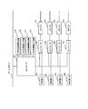
また、DSP103には、図3に示すヒストグラム作成回路が内蔵されている。図3は、ヒストグラム作成回路を示すブロック図である。同図では比較のためのコンパレータが4つの場合を示している。
Further, the
このヒストグラム作成回路には、画像データが入力される入力ライン201が設けられている。さらに、入力ライン201に画像データが入力されると、当該画像データが演算領域503内のものであるか否かを判定するコントローラ202が設けられている。コントローラ202には、レジスタ215、216、217及び218が接続されている。レジスタ215、216、217、218には、夫々、V方向演算開始位置、V方向演算終了位置、H方向演算開始位置、H方向演算終了位置を示す値が設定される。コントローラ202は、レジスタ215〜218に設定された値を参照し、入力された画像データが演算領域503内のものであれば、画素出力を複数のコンパレータ207、208、209及び210に出力する。
The histogram creation circuit is provided with an input line 201 for inputting image data. Further, a
コンパレータ207、208、209、210は、夫々に対して設けられたレジスタ203、204、205、206に設定されている判定値Th1、Th2、Th3、Th4と対象画素出力とを比較する。ここで、判定値Th1〜Th4の間には、「Th1<Th2<Th3<Th4」の関係が成立している。なお、判定値Th1〜Th4は、ROM106又はRAM107に記憶されており、撮影前に各レジスタ203〜206に設定される。
The
また、コンパレータ207〜210の後段には夫々計数カウンタ211、212、213、214が接続されており、演算領域503内で各判定値Th1、Th2、Th3、Th4を超える出力を示した画素数を計数し、記憶する。計数カウンタ211〜214の出力信号は読み出し可能となっており、CPU105が計数カウンタ211〜214の出力信号を用いて判定を行う。つまり、計数カウンタ211〜214によるカウント値に基づいて暗電流の量が求められる。
Further, counters 211, 212, 213, and 214 are connected to the subsequent stages of the
従って、レジスタ215〜218の各々に、演算領域503の位置を示す値を設定しておけば、演算領域503の読み出しが終了した時点で、計数カウンタ211〜214には、それぞれの判定値Th1〜Th4を超える画素の個数が記憶されていることとなる。そして、この個数は累積ヒストグラムを示していることとなる。
Accordingly, if a value indicating the position of the calculation area 503 is set in each of the
ここで、判定値Th1〜Th4を求める方法について説明する。暗電流の量(レベル)及び白キズの発生については、次のような自然現象が存在する。
(a)露光時間が長くなったり、撮像素子の温度が高くなったりすると、暗電流のレベルも大きくなる。
(b)露光時間が長くなったり、撮像素子の温度が高くなったりすると、露光時間が短い時や温度が低い時には見えなかった、微小キズ(白キズ)が目立つようになる。更に、微小キズのレベルも、露光時間や撮像素子の温度によって変化する。
Here, a method for obtaining the determination values Th1 to Th4 will be described. The following natural phenomena exist regarding the amount (level) of dark current and the occurrence of white flaws.
(A) When the exposure time is increased or the temperature of the image sensor is increased, the dark current level is also increased.
(B) When the exposure time is long or the temperature of the image sensor is high, fine scratches (white scratches) that cannot be seen when the exposure time is short or when the temperature is low become conspicuous. Furthermore, the level of minute flaws also changes depending on the exposure time and the temperature of the image sensor.
そこで、本実施形態では、これらの自然現象に基づき、微小キズのレベルから暗電流の量を推定することとする。そして、微小キズのレベルの判定に当たり、判定値Th1〜Th4を使用する。つまり、判定値Th1〜Th4は微小キズのレベルの判定基準となる値である。図4A乃至図4Dは、ダーク画像のヒストグラムを露光時間の順に示す図である。また、図5A乃至図5Dは、ダーク画像の累積ヒストグラムを露光時間の順に示す図である。 Therefore, in the present embodiment, the amount of dark current is estimated from the level of minute scratches based on these natural phenomena. Then, the determination values Th1 to Th4 are used for determining the level of minute scratches. That is, the determination values Th1 to Th4 are values serving as determination criteria for the level of minute scratches. 4A to 4D are diagrams showing histograms of dark images in order of exposure time. 5A to 5D are diagrams showing cumulative histograms of dark images in order of exposure time.
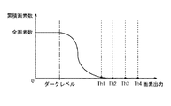
図4Aに示すように、露光時間が非常に短い場合、暗電流はほとんど発生しない。このため、ヒストグラムは設定されたダークレベルを中心に分布している。僅かなばらつきはほぼランダムノイズに相当する。この条件では白キズはほとんど存在しない。図5Aは、このときの累積ヒストグラムを示している。図5Aに示すように、画素の累積個数は、ダークレベル付近から下降しはじめ、ダークレベルとランダムノイズとの総和の近傍において累積個数がほぼ0となる。ここで、累積ヒストグラムにおいてダークレベルがあるしきい値となる点を「判定値Th1」とする。 As shown in FIG. 4A, when the exposure time is very short, dark current hardly occurs. Therefore, the histogram is distributed around the set dark level. A slight variation corresponds to almost random noise. Under these conditions, there are almost no white scratches. FIG. 5A shows a cumulative histogram at this time. As shown in FIG. 5A, the cumulative number of pixels starts to decrease from around the dark level, and the cumulative number becomes almost zero near the sum of the dark level and random noise. Here, a point at which the dark level is a certain threshold in the cumulative histogram is referred to as “determination value Th1”.
図4Bに示すように、露光時間が若干長くなると、ヒストグラムに、ダークレベルを中心とする分布に加えて、ダークレベルよりも出力が大きいところに小さな分布が出現する。即ち、白キズが発生し始める。以下、この分布を第1の微小キズグループとよぶ。第1の微小キズグループは、撮像素子の全画素中にある割合で同程度の出力を示す結晶欠陥が発生していることを示している。なお、ある撮影条件下で発生するキズグループの分布のレベルは、撮影条件を変えてもほぼ同じような出力となることが知られている。このような露光時間で得られる累積ヒストグラムには、図5Bに示すように、平坦部が現れる。この平坦部から第1の微小キズグループに属する白キズの個数A1を特定することができる。 As shown in FIG. 4B, when the exposure time is slightly increased, a small distribution appears in the histogram where the output is larger than the dark level in addition to the distribution centered on the dark level. That is, white scratches begin to occur. Hereinafter, this distribution is referred to as a first minute scratch group. The first micro-scratch group indicates that a crystal defect that shows the same level of output at a certain ratio in all the pixels of the image sensor has occurred. It is known that the level of the distribution of flaw groups that occurs under a certain shooting condition produces substantially the same output even if the shooting condition is changed. In the cumulative histogram obtained with such an exposure time, a flat portion appears as shown in FIG. 5B. The number A1 of white scratches belonging to the first minute scratch group can be specified from the flat portion.
図4Cに示すように、更に露光時間が長くなると、ヒストグラムに、ダークレベルを中心とする分布に加えて、ダークレベルよりも出力が大きいところに小さな分布が2つ出現する。出力が大きい方の分布は、図4Bにも現れている第1の微小キズグループの出力が更に増加したものであり、出力が小さい方の分布は新しく発生したものである。以下、後者の分布を第2の微小キズグループとよぶ。第2の微小キズグループは、第1の微小キズグループとは異なるが、同じ振る舞いを示す欠陥画素が発生していることを示している。このとき、ダークレベル付近の分布も全体が広がる様子を示している。これは、露光時間の延長により、更にランダムノイズが増加しているためである。このような露光時間で得られる累積ヒストグラムには、図5Cに示すように、第2の微小キズグループが出現したことを示す変化として段差が現れる。但し、この時点では、第2の微小キズグループに属する白キズの個数A2を特定することはできない。 As shown in FIG. 4C, when the exposure time is further increased, two small distributions appear in the histogram where the output is larger than the dark level in addition to the distribution centered on the dark level. The distribution with the larger output is a further increase in the output of the first micro-scratch group that also appears in FIG. 4B, and the distribution with the smaller output is a newly generated distribution. Hereinafter, the latter distribution is referred to as a second minute scratch group. The second minute scratch group is different from the first minute scratch group, but indicates that defective pixels having the same behavior are generated. At this time, the distribution in the vicinity of the dark level is also shown to spread. This is because random noise further increases due to the extension of the exposure time. In the cumulative histogram obtained with such an exposure time, a step appears as a change indicating that the second minute flaw group has appeared, as shown in FIG. 5C. However, at this time, the number A2 of white scratches belonging to the second minute scratch group cannot be specified.
図4Dに示すように、更に露光時間が長くなると、ヒストグラムに、ダークレベルを中心とする分布に加えて、ダークレベルよりも出力が大きいところに小さな分布が存在している。いずれも、第1の微小キズグループ、第2の微小キズグループの出力が更に増加してことを示している。そして、このような露光時間で得られる累積ヒストグラムには、図5Dに示すように、図5Aの平坦部よりも高い平坦部が現れる。この平坦部から第1の微小キズグループに属する白キズの個数A1と第2の微小キズグループに属する白キズの個数A2との和を特定することができる。従って、第2の微小キズグループに属する白キズの個数A2を特定することができる。更に、第2の微少キズグループのキズが、累積ヒストグラム上で平坦となる範囲の最大の点を「判定値Th4」とする。そして、判定値Th1から判定値Th4までの間を3等分して、夫々を「判定値Th2」、「判定値Th3」とする。 As shown in FIG. 4D, when the exposure time is further increased, a small distribution is present in the histogram where the output is larger than the dark level in addition to the distribution centered on the dark level. In either case, the output of the first minute scratch group and the second minute scratch group is further increased. Then, in the cumulative histogram obtained with such an exposure time, a flat portion higher than the flat portion in FIG. 5A appears as shown in FIG. 5D. From this flat portion, the sum of the number A1 of white scratches belonging to the first minute scratch group and the number A2 of white scratches belonging to the second minute scratch group can be specified. Therefore, the number A2 of white scratches belonging to the second minute scratch group can be specified. Further, the maximum point in a range where the scratch of the second minute scratch group becomes flat on the cumulative histogram is set as “determination value Th4”. Then, the interval from the determination value Th1 to the determination value Th4 is divided into three equal parts, which are set as “determination value Th2” and “determination value Th3”, respectively.
なお、判定値Th1〜Th4の設定は、例えば製造段階で行っておくが、自動キャリブレーション又はマニュアルキャリブレーションにより設定されるようにしてもよい。また、図4A〜図4D、図5A〜図5D及び図6A〜図6Dには、露光時間に応じたヒストグラム及び累積ヒストグラムの変化を表しているが、同様の傾向が温度を変化させた場合にも見られる。従って、温度を変化させながらヒストグラム及び累積ヒストグラムを作成することにより、判定値Th1〜Th4を決定することも可能である。 The determination values Th1 to Th4 are set at the manufacturing stage, for example, but may be set by automatic calibration or manual calibration. 4A to 4D, FIGS. 5A to 5D, and FIGS. 6A to 6D show changes in the histogram and the cumulative histogram according to the exposure time, but when the same tendency changes the temperature. Can also be seen. Therefore, it is also possible to determine the determination values Th1 to Th4 by creating a histogram and a cumulative histogram while changing the temperature.
これらのヒストグラム及び累積ヒストグラムは、撮像素子毎に相違しているが、同一の工程を経て製造された撮像素子間では、大きな相違は存在しない。そこで、本実施形態では、実際に製造する撮像素子と同一の工程を経て複数のサンプルを予め製造し、これらのサンプルについて累積ヒストグラムを作成する。そして、代表的な累積ヒストグラムから、上述のようにして図6A乃至図6Dに示すような判定値Th1〜Th4を設定する。なお、代表的なヒストグラムとしては、例えば、各累積ヒストグラムの平均をとったもの、最も中間に位置するもの等を用いることができる。 These histograms and cumulative histograms are different for each image sensor, but there is no significant difference between image sensors manufactured through the same process. Therefore, in the present embodiment, a plurality of samples are manufactured in advance through the same process as an image sensor actually manufactured, and a cumulative histogram is created for these samples. Then, determination values Th1 to Th4 as shown in FIGS. 6A to 6D are set from the representative cumulative histogram as described above. In addition, as a representative histogram, for example, an average of each cumulative histogram, a most intermediate histogram, or the like can be used.
なお、判定値Th1〜Th4の設定に際して、各サンプルの累積ヒストグラムから上記基準に基づいて判定値Th1〜Th4を求め、それらの平均値を求めてもよい。 Note that when setting the determination values Th1 to Th4, the determination values Th1 to Th4 may be obtained from the cumulative histogram of each sample based on the above-mentioned standard, and the average value thereof may be obtained.
次に、上述のように構成された撮像装置の制御方法について説明する。図7は、本発明の実施形態に係る撮像装置の制御方法を示すフローチャートである。この制御は、主にCPU105により実行される。
Next, a method for controlling the imaging apparatus configured as described above will be described. FIG. 7 is a flowchart illustrating a method for controlling the imaging apparatus according to the embodiment of the present invention. This control is mainly executed by the
先ず、ステップS201において電源スイッチ109がONされているか否かを判定し、ONになっていることを検出するまでこの判定を繰り返す。そして、電源スイッチ109がONにされると、ステップS203へ進む。
First, in step S201, it is determined whether or not the
ステップS203では、モードダイアル112が撮影モードに設定されているか否かを判定する。撮影モードに設定されていればステップS205へ進み、その他のモードに設定されていればステップS204に進む。ステップS204では、選択されているモードに応じた処理を行い、その終了後にステップS201へと戻る。
In step S203, it is determined whether or not the
ステップS205では、シャッタースイッチ110がONしているか否かを判定し、ONになっていることを検出するまでこの判定を繰り返す。そして、シャッタースイッチ110がONにされると、ステップS206に進む。
In step S205, it is determined whether or not the
ステップS206では、不図示の測光制御部及び測距制御部を用いて、絞り値及びシャッター速度を決定する測光処理、撮影レンズ焦点を被写体に合わせる測距処理を行う。 In step S206, using a photometry control unit and a distance measurement control unit (not shown), photometry processing for determining the aperture value and shutter speed and distance measurement processing for adjusting the photographing lens focus to the subject are performed.
次に、ステップS207において、シャッタースイッチ111がONしているか否かを判定し、ONになっていることを検出するまでこの判定を繰り返す。そして、シャッタースイッチ111がONにされると、ステップS208に進む。
Next, in step S207, it is determined whether or not the
ステップS208では、撮影処理を実行する。この撮影処理の詳細については後述する。 In step S208, shooting processing is executed. Details of this photographing process will be described later.
次に、ステップS210において、DSP103に撮影した画像データの現像処理を行わせる。続いて、ステップS211において、DSP103に現像処理の終了した画像データに対する圧縮処理を行わせ、RAM107の空き領域に格納させる。
Next, in step S210, the
そして、ステップS212において、RAM107に格納されている画像データをDSP103に読み出させ、記録媒体108への記録処理を実行させる。記録処理終了後に、ステップS201へ戻り、次の撮影に備える。
In step S212, the image data stored in the
次に、ステップS208の撮影処理の詳細について、図8を参照しながら説明する。図8は、撮影処理の内容を示すフローチャートである。 Next, details of the photographing process in step S208 will be described with reference to FIG. FIG. 8 is a flowchart showing the contents of the photographing process.
先ず、ステップS301において、ミラーをミラーアップ位置に移動させる。次に、ステップS302において、ステップS205の測光処理において取得した測光データに基づいて、所定の絞り値まで絞りを駆動する。次いで、ステップS303において、撮像素子101の電荷を消去する(クリア)。その後、ステップS304において、撮像素子101での電荷蓄積を開始する。続いて、ステップS305において、シャッターを開き、ステップS306にて撮像素子101の露光を開始する。
First, in step S301, the mirror is moved to the mirror up position. Next, in step S302, the aperture is driven to a predetermined aperture value based on the photometric data acquired in the photometric processing in step S205. Next, in step S303, the charge of the
そして、ステップS307において、測光データに従って露光終了時間が経過するまで待機し、露光終了時間が経過すると、ステップS308において、シャッターを閉じる。 In step S307, the process waits until the exposure end time elapses according to the photometric data. When the exposure end time elapses, the shutter is closed in step S308.
次に、ステップS309において、開放の絞り値まで絞りを駆動する。次いで、ステップS310において、ミラーダウン位置までミラーを駆動する。その後、ステップS311において、設定した電荷蓄積時間が経過するまで待機し、電荷蓄積時間が経過すると、ステップS312において、撮像素子101の電荷蓄積を終了する。
Next, in step S309, the aperture is driven to the full aperture value. Next, in step S310, the mirror is driven to the mirror down position. Thereafter, in step S311, the process waits until the set charge accumulation time elapses. When the charge accumulation time elapses, the charge accumulation of the
続いて、ステップS313において、撮像素子101の信号を読み出す。この処理に際して、撮像子101はアンプゲインをISO感度設定スイッチ113にて設定されているISO感度に応じたゲイン値に切り替えておく。また、ダークオフセットレベルをクランプする機能を具えたAFE102は、撮像素子101のオプティカルブラック部501からの出力を用いて、クランプ動作を行う。
Subsequently, in step S313, the signal of the
更に、読み出し開始と同時にステップS314にてDSP103が暗電流の推定行う。暗電流の推定の詳細については後述する。
Further, simultaneously with the start of reading, the
その後、ステップS315において、CPU105が、ステップS314で検出した暗電流の量を、事前に設定されROM106又はRAM107に記憶されている基準値と比較する。この基準値は、例えばノイズリダクション処理が必要とされる暗電流量とする。そして、暗電流値が基準値未満であればそのまま終了し、基準値以上であればステップS316に進む。ステップS316では、ノイズリダクション処理を行う。ノイズリダクション処理の詳細については後述する。
Thereafter, in step S315, the
そして、これらの処理が終了すると、撮影処理が終了し、ステップS210へと進む。 When these processes are finished, the photographing process is finished, and the process proceeds to step S210.
次に、ステップS314の暗電流の推定処理について説明する。上述のように、本実施形態では、暗電流の量を微小キズのレベルから推定する。この推定処理は、コンパレータ207〜210が対象画素出力を判定値Th1〜Th4と比較し、その結果を計数カウンタ211〜214が計数することにより、実行される。即ち、計数カウンタ211〜214のカウント値から微小キズのレベルが特定され、この微小キズのレベルから暗電流の量が推定される。つまり、この暗電流の推定処理はDSP103により実行される。
Next, the dark current estimation processing in step S314 will be described. As described above, in the present embodiment, the amount of dark current is estimated from the level of minute scratches. This estimation process is executed when the
ここで、計数カウンタ211〜214のカウント値と、微小キズのレベル及び暗電流量(ダークレベル)との関係について説明する。この関係をまとめると図9のようになる。図9中のダークレベルの「Dark0」〜「Dark9」には、予め実測した値があてはめられる。「Dark0」〜「Dark9」の順で暗電流量が大きくなっており、「Dark0」の場合には、ステップS315において判定値未満としてノイズリダクション処理(ステップS316)を行わないようにしてもよい。
Here, the relationship between the count values of the counting counters 211 to 214, the level of minute scratches, and the dark current amount (dark level) will be described. This relationship is summarized as shown in FIG. The dark levels “
ここで、「L」は、計数カウンタ211〜214のカウント値が「0〜0+N1」であることを示している。また、「M1」は、計数カウンタ211〜214のカウント値が「(白キズの個数A1−N2)〜(白キズの個数A1+N2)」であることを示している。また、「M2」は、計数カウンタ211〜214のカウント値が「(白キズの個数A1及びA2の総和−N3)〜(白キズの個数A1及びA2の総和+N3)」であることを示している。また、「M3」は、計数カウンタ211〜214のカウント値が「白キズの個数A1及びA2の総和+N4以上」であることを示している。なお、「N1」は「判定値Th1」を決定する際に参照したダークレベルのしきい値である。また、「N2」、「N3」及び「N4」は、白キズの個数A1及びA2のばらつき等を考慮したマージンであり、任意に設定することができる。なお、第1の微小キズグループのレベルと第2の微小キズグループのレベルとの間には比較的大きな差が存在するため、「L」、「M1」、「M2」及び「M3」が互いに重なり合わない範囲でマージンN1〜N4を大きく設定しても不都合は生じない。 Here, “L” indicates that the count values of the count counters 211 to 214 are “0 to 0 + N1”. “M1” indicates that the count values of the count counters 211 to 214 are “(number of white scratches A1−N2) to (number of white scratches A1 + N2)”. “M2” indicates that the count values of the count counters 211 to 214 are “(total number of white scratches A1 and A2−N3) to (total sum of white scratches A1 and A2 + N3)”. Yes. “M3” indicates that the count value of the count counters 211 to 214 is “the sum of the number of white scratches A1 and A2 + N4 or more”. Note that “N1” is a dark level threshold value referred to when the “determination value Th1” is determined. “N2”, “N3”, and “N4” are margins that take into account variations in the number of white scratches A1 and A2, and can be arbitrarily set. Since there is a relatively large difference between the level of the first micro-scratch group and the level of the second micro-scratch group, “L”, “M1”, “M2”, and “M3” are mutually different. There is no inconvenience even if the margins N1 to N4 are set large within a range where they do not overlap.
これらの基準値を図示すると、図10のようになる。図10には、累積ヒストグラムの一例も記載してある。この例では、計数カウンタ211〜214のカウント値がいずれも「M2」に該当するため、ダークレベルは「Dark8」となる(図9)。そして、「Dark8」の暗電流量は、予め行われている実測により求められているため、この量に応じたノイズリダクション処理(ステップS316)を行えばよいことになる。 These reference values are illustrated in FIG. FIG. 10 also shows an example of a cumulative histogram. In this example, since the count values of the counting counters 211 to 214 all correspond to “M2”, the dark level is “Dark8” (FIG. 9). Since the dark current amount of “Dark8” is obtained by actual measurement performed in advance, noise reduction processing (step S316) corresponding to this amount may be performed.
次に、ノイズリダクション処理について図11のフローチャートを参照しながら説明する。なお、ここでいうところのノイズリダクション処理とは、本画像から同時間蓄積したダーク画像の減算処理を意味する。 Next, the noise reduction process will be described with reference to the flowchart of FIG. Note that the noise reduction processing here means subtraction processing of a dark image accumulated for the same time from the main image.
ノイズリダクション処理を開始する以前では、先に撮影した本画像は未だ現像処理に進んでいないので、一時的にRAM107に保存されている。
Prior to the start of the noise reduction process, the previously captured main image has not yet proceeded to the development process, and is temporarily stored in the
ノイズリダクション処理が始まると、先ず、ステップS401にて再度撮像素子の電荷をクリアし、ステップS402にて電荷蓄積を開始する。このシーケンスではダーク画像の取得を目標としているため、電荷蓄積開始後にシャッターを開くことはない。 When the noise reduction process starts, first, the charge of the image sensor is cleared again in step S401, and charge accumulation is started in step S402. Since this sequence aims to acquire a dark image, the shutter is not opened after the start of charge accumulation.
ステップS403にて設定された本画像の露光時間と同じ時間が経過したかどうかを判定する。そして、ステップS403にて設定時間が経過していれば、ステップS404にて、撮像素子101の電荷蓄積を終了する。
It is determined whether or not the same time as the exposure time of the main image set in step S403 has elapsed. If the set time has elapsed in step S403, the charge accumulation of the
このようにして得られたダーク画像の信号を、ステップS405にて撮像素子101の信号として読み出す。この時、撮像素子101はアンプゲインを本画像撮影時と同様に、ISO感度設定スイッチ113にて設定されているISO感度に応じたゲイン値に切り替えておく。
The dark image signal thus obtained is read out as a signal of the
読み出した画像データは一時的にRAM107に保存する。次に、ステップS407にて本画像からダーク画像の減算処理を行う。この減算処理では、ステップS314において推定された暗電流量を考慮した上で、RAM107に保存されている本画像データから、ダーク画像データの各画素毎の減算処理及びダークオフセットの加算処理を行う。
The read image data is temporarily stored in the
このような処理を行ったデータは一時的にRAM107に保存してもよいし、そのままステップS210の現像処理に進めてもよい。また、このような減算処理が終了した時点でRAM107上の本画像データ及びダーク画像データは不要となるので、消去してもよい。このようにして、ノイズリダクション処理(ステップS316)が終了する。
The data that has undergone such processing may be temporarily stored in the
このような本実施形態によれば、図9に示すテーブルから、計数カウンタ211〜214の計数カウンタ値から微小キズグループの分布を特定し、暗電流量を容易に推定することができる。そして、効果的なノイズリダクション処理を実行することができる。 According to the present embodiment as described above, it is possible to easily estimate the dark current amount by specifying the distribution of minute scratch groups from the count counter values of the count counters 211 to 214 from the table shown in FIG. Then, effective noise reduction processing can be executed.
なお、上述の実施形態では、判定値の判定用に4個のコンパレータを用いているが、判定値をより細かくし、コンパレータ及び計数カウンタの組数を多くすることにより、更に高精度に特定のレベルのキズグループの分布を判定することが可能となる。このようにより多くの判定値を用いた場合には、判定手法もより高精度に行う必要があるが、基本的には、上述のように、ある特定のキズレベルを持つキズ画素のグループがどの判定値付近にいるかを検出できればよい。そして、これを実現する方法としては、連続点の線形近似等の多くの方法が考えられる。 In the above-described embodiment, four comparators are used for determining the determination value. However, by making the determination value finer and increasing the number of sets of comparators and count counters, the specific value can be specified with higher accuracy. It becomes possible to determine the distribution of level scratch groups. When more determination values are used in this way, the determination method also needs to be performed with higher accuracy. However, basically, as described above, the determination of which group of flaw pixels having a specific flaw level is present. What is necessary is just to be able to detect whether it is near the value. As a method for realizing this, many methods such as linear approximation of continuous points can be considered.
また、あるキズ画素のグループのある条件下での出力値を事前に確認しておけば、その後に得た画像からある特定のキズレベルを持つキズ画素のグループがどの判定値付近にいるか検出すると、その時点で得られた出力値と基準の出力値とを比較することもできる。これらの条件下での出力値の換算を行うことにより、その時点での出力値を想定することが可能となる。 In addition, if the output value under a certain condition of a certain scratch pixel group is confirmed in advance, it is detected which judgment value is near a group of scratch pixels having a specific scratch level from an image obtained thereafter. It is also possible to compare the output value obtained at that time with the reference output value. By converting the output value under these conditions, the output value at that time can be assumed.
よく知られているように、温度が8℃〜10℃上昇すると出力が2倍になり、露光時間、ISO感度に比例するといった単純な計算のみを用いることで演算可能である。例えば、基準条件としてISO800、25℃、露光時間1秒で撮影したとき、第1の微小キズグループの分布中心が10mV、第2の微小キズグループの分布中心が5mVであったとする。なお、ここでは、画素出力を仮の電圧値で表している。 As is well known, when the temperature rises by 8 ° C. to 10 ° C., the output doubles and can be calculated using only a simple calculation that is proportional to the exposure time and ISO sensitivity. For example, it is assumed that when the image is taken with ISO 800, 25 ° C. and an exposure time of 1 second as the reference conditions, the distribution center of the first minute scratch group is 10 mV and the distribution center of the second minute scratch group is 5 mV. Here, the pixel output is represented by a temporary voltage value.
そして、本画像としてISO400、露光時間8秒で撮影した画像のVOB部の出力を判定したときに、第1の微小キズグループが上述の判定方法により、60mV〜100mVの間に存在すると判定されたとする。ここで、60mV及び100mVは、判定値Th1〜Th4のいずれかである。 Then, when the output of the VOB portion of the image taken at ISO 400 and the exposure time of 8 seconds is determined as the main image, it is determined that the first minute scratch group is present between 60 mV and 100 mV by the above-described determination method. To do. Here, 60 mV and 100 mV are any of the determination values Th1 to Th4.
この場合、撮影条件から換算すると、基準条件と比較し、露光時間が8倍で、ISO感度が1/2であるので、撮像素子の温度が25℃であると仮定すると、第1の微小キズグループの分布中心は40mV付近に存在するはずである。これに対し、実測結果では約2倍の60mV〜100mVに存在しているのだから、約2倍の出力であると予測することができ、撮像素子の温度は25℃よりも約8℃〜10℃程度高いことと予想することができる。 In this case, when converted from the shooting conditions, the exposure time is 8 times and the ISO sensitivity is ½ compared to the reference conditions. Therefore, assuming that the temperature of the image sensor is 25 ° C., the first minute scratch The distribution center of the group should be around 40 mV. On the other hand, since the actual measurement result is about 60 to 100 mV, which is about twice, it can be predicted that the output is about twice, and the temperature of the image sensor is about 8 to 10 ° C. rather than 25 ° C. It can be expected to be as high as about ° C.
更に、事前に測定した温度及び平均暗電流の対応から、撮像素子の暗電流量を予測することも可能となる。例えば、事前に測定した撮像素子において、第1の微小キズグループの分布中心と平均暗電流との間の比例係数C1、及び第2の微小キズグループの分布中心と平均暗電流との間の比例係数C2を、ROM106又はRAM107に事前に記憶させておく。そして、概略値×比例係数から平均暗電流を演算することで予測することができる。例えば、上述の例であれば、第1の微小キズグループの分布中心が60mV〜100mVのとき、予想される平均暗電流は60mV×C1〜100mV×C1と予測できる。
Furthermore, it is possible to predict the dark current amount of the image sensor from the correspondence between the temperature measured in advance and the average dark current. For example, in the image sensor measured in advance, the proportional coefficient C1 between the distribution center of the first minute scratch group and the average dark current, and the proportionality between the distribution center of the second minute scratch group and the average dark current. The coefficient C2 is stored in advance in the
そして、この予測値をノイズリダクション動作を行うか否かを判定する判定値と比較することにより、ノイズに埋もれた平均暗電流を直接測定するよりも高精度に推定することが可能となる。 Then, by comparing the predicted value with a determination value for determining whether or not to perform the noise reduction operation, it is possible to estimate the average dark current buried in the noise with higher accuracy than directly measuring.
なお、上述の実施形態では、暗電流量を推定し、その結果からノイズリダクション処理を行うか否かの判定を行っているが、判定後の動作に関してはこれに限定されるものではなく、各種の補正処理、検出処理、警告処理等を行ってもよい。 In the above-described embodiment, the amount of dark current is estimated, and whether or not noise reduction processing is performed is determined from the result. However, the operation after the determination is not limited to this, Correction processing, detection processing, warning processing, and the like may be performed.
また、上述の実施形態では、累積ヒストグラムの作成をDSP103の内部に設けたヒストグラム作成回路(図3)に行わせているが、他の箇所で行ってもよいし、ソフトウェアを用いて処理を行ってもよい。
In the above-described embodiment, the cumulative histogram is created by the histogram creation circuit (FIG. 3) provided in the
更に、上述の実施形態では、VOB部501aの出力を測定し、ノイズリダクション動作を行うか否かの判定を行っているが、出力の測定対象領域は遮光領域であればどこでもよい。例えば、部分的に熱源となりうる撮像素子内のアンプ等の近傍を測定し、アンプ等の発熱の影響があるかないかという判定に用いることも可能である。また、撮像素子の遮光領域だけではなく、遮光時の開口領域における出力を測定するようにしてもよい。 Further, in the above-described embodiment, the output of the VOB unit 501a is measured and it is determined whether or not the noise reduction operation is performed. However, the output measurement target region may be any light-shielding region. For example, it is also possible to measure the vicinity of an amplifier or the like in an image sensor that can partially become a heat source, and use it to determine whether there is an influence of heat generation of the amplifier or the like. Further, not only the light shielding area of the image sensor but also the output in the opening area at the time of light shielding may be measured.
なお、本発明の実施形態は、例えばコンピュータがプログラムを実行することによって実現することができる。また、プログラムをコンピュータに供給するための手段、例えばかかるプログラムを記録したCD−ROM等のコンピュータ読み取り可能な記録媒体又はかかるプログラムを伝送するインターネット等の伝送媒体も本発明の実施形態として適用することができる。また、上記のプログラムも本発明の実施形態として適用することができる。上記のプログラム、記録媒体、伝送媒体及びプログラムプロダクトは、本発明の範疇に含まれる。 The embodiment of the present invention can be realized by, for example, a computer executing a program. Also, means for supplying a program to a computer, for example, a computer-readable recording medium such as a CD-ROM recording such a program, or a transmission medium such as the Internet for transmitting such a program is also applied as an embodiment of the present invention. Can do. The above program can also be applied as an embodiment of the present invention. The above program, recording medium, transmission medium, and program product are included in the scope of the present invention.
101:撮像素子
102:AFE
103:DSP
104:タイミング発生回路
105:CPU
106:ROM
107:RAM
108:記憶媒体
109:電源スイッチ
110、111:シャッタースイッチ
112:モードダイアル
113:ISO感度設定スイッチ
201:入力ライン
202:コントローラ
203〜206:レジスタ
207〜210:コンパレータ
211〜214:計数カウンタ
215〜218:レジスタ
101: Image sensor 102: AFE
103: DSP
104: Timing generation circuit 105: CPU
106: ROM
107: RAM
108: Storage medium 109:
Claims (7)
前記遮光画素領域の少なくとも一部から出力された遮光画素出力値と、予め設定されているダークレベルよりも大きい複数の判定値とを比較する比較手段と、
前記比較手段による比較の結果、前記遮光画素出力値が前記複数の判定値を超えた画素数を前記複数の判定値毎に計数する計数手段と、
前記計数手段による計数の結果に基づいて、前記撮像素子において生じる暗電流の量を求める演算手段と、
を有することを特徴とする撮像装置。 An image sensor including a light-shielding pixel region;
A comparison unit that compares a light-shielded pixel output value output from at least a part of the light-shielded pixel region with a plurality of determination values greater than a preset dark level ;
As a result of comparison by the comparison means, a counting means for counting the number of pixels in which the light-shielded pixel output value exceeds the plurality of determination values for each of the plurality of determination values;
An arithmetic means for obtaining an amount of dark current generated in the image sensor based on a result of counting by the counting means
An imaging device comprising:
前記遮光画素領域の少なくとも一部から出力された遮光画素出力値と、予め設定されているダークレベルよりも大きい複数の判定値とを比較する比較ステップと、
前記比較ステップにおける比較の結果、前記遮光画素出力値が前記複数の判定値を超えた画素数を前記複数の判定値毎に計数する計数ステップと、
前記計数ステップにおける計数の結果に基づいて、前記撮像素子において生じる暗電流の量を求める演算ステップと、
を有することを特徴とする撮像装置の制御方法。 A method for controlling an imaging apparatus having an imaging element including a light-shielding pixel region,
A comparison step of comparing a light-shielded pixel output value output from at least a part of the light-shielded pixel region with a plurality of determination values greater than a preset dark level ;
As a result of the comparison in the comparison step, a counting step for counting the number of pixels in which the light-shielded pixel output value exceeds the plurality of determination values for each of the plurality of determination values;
A calculation step for obtaining the amount of dark current generated in the image sensor based on the counting result in the counting step;
A method for controlling an imaging apparatus, comprising:
Priority Applications (2)
| Application Number | Priority Date | Filing Date | Title |
|---|---|---|---|
| JP2006194755A JP4921058B2 (en) | 2006-07-14 | 2006-07-14 | Imaging apparatus and control method thereof |
| US11/775,725 US8436923B2 (en) | 2006-07-14 | 2007-07-10 | Imaging apparatus having a function for estimating a dark current amount |
Applications Claiming Priority (1)
| Application Number | Priority Date | Filing Date | Title |
|---|---|---|---|
| JP2006194755A JP4921058B2 (en) | 2006-07-14 | 2006-07-14 | Imaging apparatus and control method thereof |
Publications (3)
| Publication Number | Publication Date |
|---|---|
| JP2008022486A JP2008022486A (en) | 2008-01-31 |
| JP2008022486A5 JP2008022486A5 (en) | 2009-08-27 |
| JP4921058B2 true JP4921058B2 (en) | 2012-04-18 |
Family
ID=38948857
Family Applications (1)
| Application Number | Title | Priority Date | Filing Date |
|---|---|---|---|
| JP2006194755A Expired - Fee Related JP4921058B2 (en) | 2006-07-14 | 2006-07-14 | Imaging apparatus and control method thereof |
Country Status (2)
| Country | Link |
|---|---|
| US (1) | US8436923B2 (en) |
| JP (1) | JP4921058B2 (en) |
Families Citing this family (6)
| Publication number | Priority date | Publication date | Assignee | Title |
|---|---|---|---|---|
| US8805071B2 (en) | 2008-06-30 | 2014-08-12 | Kyocera Corporation | Image processing method an imaging device module |
| US8035073B2 (en) * | 2008-11-25 | 2011-10-11 | Analog Devices, Inc. | Switched capacitor input stage for imaging front-ends |
| JP5523065B2 (en) * | 2009-11-13 | 2014-06-18 | キヤノン株式会社 | Imaging apparatus and control method thereof |
| CN102970549B (en) * | 2012-09-20 | 2015-03-18 | 华为技术有限公司 | Image processing method and image processing device |
| US9560294B2 (en) * | 2014-12-10 | 2017-01-31 | Semiconductor Components Industries, Llc | Systems and methods for pixel-level dark current compensation in image sensors |
| US12174071B2 (en) | 2022-05-13 | 2024-12-24 | Verity Instruments, Inc. | System, apparatus, and method for improved background correction and calibration of optical devices |
Family Cites Families (8)
| Publication number | Priority date | Publication date | Assignee | Title |
|---|---|---|---|---|
| JPH07117571B2 (en) * | 1988-09-22 | 1995-12-18 | 松下電子工業株式会社 | Inspection method for solid-state image sensor |
| US7259787B2 (en) * | 2003-03-27 | 2007-08-21 | Eastman Kodak Company | Digital black clamp circuit in electronic imaging systems |
| US7563748B2 (en) | 2003-06-23 | 2009-07-21 | Cognis Ip Management Gmbh | Alcohol alkoxylate carriers for pesticide active ingredients |
| EP1655957A4 (en) * | 2003-07-01 | 2009-03-18 | Nikon Corp | DEVICE FOR CORRECTING THE VIDEO SIGNAL OF AN ELECTRONIC CAMERA |
| US20050030412A1 (en) * | 2003-08-07 | 2005-02-10 | Canon Kabushiki Kaisha | Image correction processing method and image capture system using the same |
| JP4411053B2 (en) * | 2003-11-06 | 2010-02-10 | キヤノン株式会社 | IMAGING DEVICE, ITS CONTROL METHOD, CONTROL PROGRAM, AND STORAGE MEDIUM |
| TWI285047B (en) * | 2005-11-24 | 2007-08-01 | Sunplus Technology Co Ltd | Method of automatic exposure control and automatic exposure compensated apparatus |
| JP4554504B2 (en) * | 2005-12-16 | 2010-09-29 | 富士通セミコンダクター株式会社 | Image data processing circuit and image data processing method |
-
2006
- 2006-07-14 JP JP2006194755A patent/JP4921058B2/en not_active Expired - Fee Related
-
2007
- 2007-07-10 US US11/775,725 patent/US8436923B2/en not_active Expired - Fee Related
Also Published As
| Publication number | Publication date |
|---|---|
| US20080012965A1 (en) | 2008-01-17 |
| US8436923B2 (en) | 2013-05-07 |
| JP2008022486A (en) | 2008-01-31 |
Similar Documents
| Publication | Publication Date | Title |
|---|---|---|
| US7280141B1 (en) | Fixed pattern noise subtraction in a digital image sensor | |
| JP5335327B2 (en) | Defect detection and correction apparatus and defect detection and correction method | |
| JP5561112B2 (en) | Image processing apparatus, imaging apparatus, and program | |
| JP2004112802A (en) | Digital image sensor and method for detecting defective pixels | |
| JPH10322603A (en) | Electronic camera | |
| CN101800859A (en) | Shooting method and apparatus for taking multiple shots using multiple light metering modes | |
| CN101014091A (en) | Image pickup apparatus and control method thereof | |
| US20090310849A1 (en) | Defective pixel processing device and defective pixel processing method | |
| WO2020241471A1 (en) | Calibration method | |
| US8436923B2 (en) | Imaging apparatus having a function for estimating a dark current amount | |
| KR101072945B1 (en) | Apparatus for balancing flashed image color using depth estimation and method therefor | |
| CN107454388A (en) | Image processing method and the device using this method | |
| JP6118133B2 (en) | Signal processing apparatus and imaging apparatus | |
| JP2018007083A (en) | Image processing apparatus | |
| JPWO2005004467A1 (en) | Video signal correction device for electronic camera | |
| JP2013207611A (en) | Imaging device | |
| JP2013162173A (en) | Imaging apparatus and program | |
| KR101429512B1 (en) | BANDING NOISE REMOVING DEVICE AND METHOD | |
| JP3767188B2 (en) | Electronic camera and signal correction method | |
| JP4901246B2 (en) | Spectral luminance distribution estimation system and method | |
| JP2009033550A (en) | Image pickup apparatus | |
| JP2007019577A (en) | Solid-state imaging device | |
| JP2009094794A (en) | Imaging apparatus and image processing method | |
| JP4525198B2 (en) | Noise removal device, electronic camera, and noise removal program. | |
| JP5653178B2 (en) | Imaging apparatus and control method thereof |
Legal Events
| Date | Code | Title | Description |
|---|---|---|---|
| A521 | Request for written amendment filed |
Free format text: JAPANESE INTERMEDIATE CODE: A523 Effective date: 20090713 |
|
| A621 | Written request for application examination |
Free format text: JAPANESE INTERMEDIATE CODE: A621 Effective date: 20090713 |
|
| A977 | Report on retrieval |
Free format text: JAPANESE INTERMEDIATE CODE: A971007 Effective date: 20110817 |
|
| A131 | Notification of reasons for refusal |
Free format text: JAPANESE INTERMEDIATE CODE: A131 Effective date: 20110823 |
|
| A521 | Request for written amendment filed |
Free format text: JAPANESE INTERMEDIATE CODE: A523 Effective date: 20111021 |
|
| TRDD | Decision of grant or rejection written | ||
| A01 | Written decision to grant a patent or to grant a registration (utility model) |
Free format text: JAPANESE INTERMEDIATE CODE: A01 Effective date: 20120124 |
|
| A01 | Written decision to grant a patent or to grant a registration (utility model) |
Free format text: JAPANESE INTERMEDIATE CODE: A01 |
|
| A61 | First payment of annual fees (during grant procedure) |
Free format text: JAPANESE INTERMEDIATE CODE: A61 Effective date: 20120202 |
|
| R151 | Written notification of patent or utility model registration |
Ref document number: 4921058 Country of ref document: JP Free format text: JAPANESE INTERMEDIATE CODE: R151 |
|
| FPAY | Renewal fee payment (event date is renewal date of database) |
Free format text: PAYMENT UNTIL: 20150210 Year of fee payment: 3 |
|
| LAPS | Cancellation because of no payment of annual fees |