JP4806678B2 - Organic light emitting diode (OLED) with improved light extraction and corresponding display unit - Google Patents
Organic light emitting diode (OLED) with improved light extraction and corresponding display unit Download PDFInfo
- Publication number
- JP4806678B2 JP4806678B2 JP2007517373A JP2007517373A JP4806678B2 JP 4806678 B2 JP4806678 B2 JP 4806678B2 JP 2007517373 A JP2007517373 A JP 2007517373A JP 2007517373 A JP2007517373 A JP 2007517373A JP 4806678 B2 JP4806678 B2 JP 4806678B2
- Authority
- JP
- Japan
- Prior art keywords
- light emitting
- reflective
- oled
- region
- electrode
- Prior art date
- Legal status (The legal status is an assumption and is not a legal conclusion. Google has not performed a legal analysis and makes no representation as to the accuracy of the status listed.)
- Expired - Fee Related
Links
Images


Classifications
-
- H—ELECTRICITY
- H10—SEMICONDUCTOR DEVICES; ELECTRIC SOLID-STATE DEVICES NOT OTHERWISE PROVIDED FOR
- H10K—ORGANIC ELECTRIC SOLID-STATE DEVICES
- H10K50/00—Organic light-emitting devices
- H10K50/80—Constructional details
- H10K50/805—Electrodes
-
- H—ELECTRICITY
- H05—ELECTRIC TECHNIQUES NOT OTHERWISE PROVIDED FOR
- H05B—ELECTRIC HEATING; ELECTRIC LIGHT SOURCES NOT OTHERWISE PROVIDED FOR; CIRCUIT ARRANGEMENTS FOR ELECTRIC LIGHT SOURCES, IN GENERAL
- H05B33/00—Electroluminescent light sources
- H05B33/12—Light sources with substantially two-dimensional [2D] radiating surfaces
- H05B33/26—Light sources with substantially two-dimensional [2D] radiating surfaces characterised by the composition or arrangement of the conductive material used as an electrode
-
- H—ELECTRICITY
- H05—ELECTRIC TECHNIQUES NOT OTHERWISE PROVIDED FOR
- H05B—ELECTRIC HEATING; ELECTRIC LIGHT SOURCES NOT OTHERWISE PROVIDED FOR; CIRCUIT ARRANGEMENTS FOR ELECTRIC LIGHT SOURCES, IN GENERAL
- H05B33/00—Electroluminescent light sources
- H05B33/12—Light sources with substantially two-dimensional [2D] radiating surfaces
- H05B33/22—Light sources with substantially two-dimensional [2D] radiating surfaces characterised by the chemical or physical composition or the arrangement of auxiliary dielectric or reflective layers
-
- H—ELECTRICITY
- H10—SEMICONDUCTOR DEVICES; ELECTRIC SOLID-STATE DEVICES NOT OTHERWISE PROVIDED FOR
- H10K—ORGANIC ELECTRIC SOLID-STATE DEVICES
- H10K50/00—Organic light-emitting devices
- H10K50/80—Constructional details
- H10K50/805—Electrodes
- H10K50/81—Anodes
- H10K50/813—Anodes characterised by their shape
-
- H—ELECTRICITY
- H10—SEMICONDUCTOR DEVICES; ELECTRIC SOLID-STATE DEVICES NOT OTHERWISE PROVIDED FOR
- H10K—ORGANIC ELECTRIC SOLID-STATE DEVICES
- H10K50/00—Organic light-emitting devices
- H10K50/80—Constructional details
- H10K50/85—Arrangements for extracting light from the devices
- H10K50/856—Arrangements for extracting light from the devices comprising reflective means
-
- H—ELECTRICITY
- H10—SEMICONDUCTOR DEVICES; ELECTRIC SOLID-STATE DEVICES NOT OTHERWISE PROVIDED FOR
- H10K—ORGANIC ELECTRIC SOLID-STATE DEVICES
- H10K50/00—Organic light-emitting devices
- H10K50/10—OLEDs or polymer light-emitting diodes [PLED]
- H10K50/14—Carrier transporting layers
- H10K50/15—Hole transporting layers
- H10K50/155—Hole transporting layers comprising dopants
-
- H—ELECTRICITY
- H10—SEMICONDUCTOR DEVICES; ELECTRIC SOLID-STATE DEVICES NOT OTHERWISE PROVIDED FOR
- H10K—ORGANIC ELECTRIC SOLID-STATE DEVICES
- H10K50/00—Organic light-emitting devices
- H10K50/10—OLEDs or polymer light-emitting diodes [PLED]
- H10K50/14—Carrier transporting layers
- H10K50/16—Electron transporting layers
- H10K50/165—Electron transporting layers comprising dopants
Landscapes
- Physics & Mathematics (AREA)
- Optics & Photonics (AREA)
- Electroluminescent Light Sources (AREA)
Description
本発明は、光取り出しが改善された有機発光ダイオード(OLED)及びそれに対応するディスプレイユニットに関する。そのダイオードは、光エレクトロニクス分野特に、信号光発生及びディスプレイ素子への応用を有する。 The present invention relates to an organic light emitting diode (OLED) with improved light extraction and a corresponding display unit. The diode has application in the field of optoelectronics, in particular signal light generation and display elements.
有機発光ダイオード(OLEDs)は大きな発展をしている。OLEDsに先行する従来の発光ダイオード(LEDs)同様、OLEDsは、複数の化合物、具体的には化合物半導体で、この場合では有機化合物、が有する能力に基づく。その能力とは、電極間に設けられているOLEDsが通電されることで、電荷つまり電子及び正孔の注入が可能となるときに発光することである。従来の有機発光ダイオード(OLED)構造は、任意で一以上の副次層によって構成される有機層を挟み、それぞれ反対の符号の電荷を注入することを意図している二の電極を基板上に有する。電極のうちの一である、正孔を注入する陽極は、光が射出面を介して当該電極を通り抜けて外へ放出できるように、従来は透明で、一般的にはインジウムスズ酸化物で構成される。もう一方の電極である、電子を注入する陰極は、従来は反射性である。基板を介した発光が起こるとき、その発光は下方すなわち後方発光である。なお基板を介して発光するので、その基板は透明でなくてはならない。それとは逆に基板の反対側で発光が起こるとき、その発光は上方すなわち前方発光である。OLEDs、特に電極作製に要求される条件に対する有機層の脆弱さを考慮すると、背面発光素子の方が製造は容易でかつより効率的である。 Organic light emitting diodes (OLEDs) are making great progress. Like conventional light emitting diodes (LEDs) that precede OLEDs, OLEDs are based on the ability of multiple compounds, specifically compound semiconductors, in this case organic compounds. The ability is to emit light when the OLEDs provided between the electrodes are energized to inject charges, that is, electrons and holes. A conventional organic light emitting diode (OLED) structure has two electrodes on a substrate that are intended to inject charges of opposite signs, optionally sandwiching an organic layer composed of one or more sublayers. Have. One of the electrodes, the anode that injects holes, is conventionally transparent and generally composed of indium tin oxide so that light can be emitted through the electrode through the emission surface. Is done. The other electrode, the cathode that injects electrons, is conventionally reflective. When light emission occurs through the substrate, the light emission is downward or backward light emission. Since the light is emitted through the substrate, the substrate must be transparent. In contrast, when light emission occurs on the opposite side of the substrate, the light emission is upward or forward light emission. Considering the fragility of the organic layer for OLEDs, especially the conditions required for electrode fabrication, the backside light emitting device is easier to manufacture and more efficient.
発生した光を通過させるようにするため、透明電極は非常に薄くなくてはならない。しかしそうすることによって、表面電気抵抗が増大し、OLED全面での均一な電流分布が失われることで、不均一な発光及び/又は、ジュール効果による致命的な温度上昇を引き起こす恐れがある。非常に薄い電極はさらに、機械的安定性及び環境に対する安定性の点で劣っているので、OLEDsの製造損失を生じさせ、かつ経年劣化を加速させてしまう。最終的に、非常に薄い電極の製造に使用される材料に依存して、相補的な副次層を構造に付加することでたとえば正孔又は電子を注入すなわち輸送する必要があるだろう。しかしこれは経済的観点から見ると欠点である。 The transparent electrode must be very thin to allow the generated light to pass through. However, by doing so, the surface electrical resistance is increased and the uniform current distribution over the entire surface of the OLED is lost, which may cause a non-uniform light emission and / or a fatal temperature increase due to the Joule effect. Very thin electrodes are further inferior in mechanical stability and environmental stability, resulting in manufacturing losses of OLEDs and accelerating aging. Eventually, depending on the material used to make the very thin electrode, it may be necessary to inject or transport eg holes or electrons by adding complementary sublayers to the structure. However, this is a drawback from an economic point of view.
従って中程度の電気光学特性が得られるように、電極の光学透明度と電極の電気・電子特性とで妥協点を探すことが必要となる。この効率を増大させる方向性で他の研究も行われており、特にOLEDで発生した光の大部分がこのダイオードを飛び出すような光取り出し器(light extractor)を付加した構造が提案されてきた。たとえば特許文献1又は特許文献2では、伝播する又は、横方向で反射される発生光は、横型反射体によって、ダイオード射出面へ戻されなければならないことも提案されてきた。
有機発光ダイオードは、基板の背面から前面にかけて、有機発光層を上にした少なくとも一の所謂背面電極、及び、それらの上に所謂前面電極を有する。特許文献3は、この場合実質的に透明な背面電極に孔を作製することによって、又はこの背面電極に突起部を供することによって、そのような発光ダイオードからの光取り出しを改善する手段について説明している。これらの孔及び突起部は、この電極表面に起伏(relief)を形成する。この電極は、特許文献3で説明されている製造法で製造されているため、この場合反射性の前面電極上で複製される。特許文献3に従うと、反射性前面電極によって形成される表面は従って、背面電極によって形成される表面と実質的に平行となる。しかし、光取り出しを改善するこの手段も依然として不十分である。特許文献4は、特許文献3で説明されている様々な取り出し方法について説明している。
The organic light emitting diode has at least one so-called back electrode with an organic light emitting layer on top from the back surface to the front surface of the substrate, and a so-called front electrode on them.
本発明は反射体を特別に実装することによって、有機発光ダイオード(OLED)からの光取り出しを増大させることを提案する。しかしそれと同時に、上記と矛盾するようだが、光がダイオードから外へ放出できるように表面積を減少させる。特別な典型的実施例に従うと、本発明は、特定構造を製造する手順及び、OLEDの光射出面上に二の側面を有する基本プリズム形状で構成される。特定構造の製造手順は任意で繰り返される。側面のうちの一面は反射性である。他の特別な典型的実施例に従うと、本発明は、前面電極平面上に突起物を有する反射領域を備える手順を有する。提案した解決法は、光がダイオードから外へ飛び出すことのできる射出面がより大きいときに、光の取り出しは相応してより効率的になりうるという原理に対抗する。提案された解決法はしかも、産業上非常に単純である。その理由は、OLEDの射出面を製造するのに、特にエンボス加工のような既知の方法を使用することが可能だからである。 The present invention proposes to increase light extraction from an organic light emitting diode (OLED) by specially mounting a reflector. But at the same time, it seems to contradict the above, but it reduces the surface area so that light can be emitted out of the diode. According to a special exemplary embodiment, the present invention consists of a procedure for manufacturing a specific structure and a basic prism shape having two sides on the light exit surface of the OLED. The manufacturing procedure for the specific structure is optionally repeated. One of the side surfaces is reflective. According to another special exemplary embodiment, the present invention comprises a procedure comprising a reflective region with protrusions on the front electrode plane. The proposed solution counters the principle that when the exit surface from which light can jump out of the diode is larger, the light extraction can be correspondingly more efficient. The proposed solution is still very simple in the industry. The reason is that it is possible to use known methods, such as embossing, in particular for producing the OLED emission surface.
本発明は従って、基板背面から前面にかけて、有機発光層を上にする、少なくとも一の所謂第1型背面電極及び、それ自体の上に少なくとも一の所謂第2型前面電極を有する有機発光ダイオード(OLED)であって、前記電極を介して電流が流れることで前記有機発光層に正孔及び電子が注入されるときに前記有機発光層が光を発生させ、前記電極の型は陽極と陰極に対応し、前記発生光が、射出面と呼ばれる前記ダイオードの面のうちの一面を介して外へ飛び出すことができるように、前記電極のうちの少なくとも一は、前記発生光に対して実質的に透明であることを特徴とする有機発光ダイオード(OLED)に関する。 The present invention therefore provides an organic light emitting diode having at least one so-called first type back electrode with the organic light emitting layer facing up from the back side of the substrate to the front side and at least one so-called second type front electrode on itself ( OLED), and when holes and electrons are injected into the organic light emitting layer due to current flowing through the electrode, the organic light emitting layer generates light, and the type of the electrode is an anode and a cathode. Correspondingly, at least one of the electrodes is substantially relative to the generated light so that the generated light can jump out through one of the faces of the diode called the exit surface. The present invention relates to an organic light emitting diode (OLED) characterized by being transparent.
本発明に従うと、
前記実質的に透明な電極は、少なくとも一の透明取り出し領域及び、少なくとも一の反射領域を有し、前記発光層を介することで前記発生光を戻す。
According to the present invention,
The substantially transparent electrode has at least one transparent extraction region and at least one reflection region, and returns the generated light through the light emitting layer.
前記ダイオードはまた、前記有機発光層からみて前記実質的に透明な電極の反対側に備えられていて、前記発光層を介して前記実質的に透明な電極へ前記発生光を戻す反射体を有する。 The diode also includes a reflector that is provided on the opposite side of the substantially transparent electrode from the organic light emitting layer and returns the generated light to the substantially transparent electrode through the light emitting layer. .
前記発生光の取り出し領域を有する前記実質的に透明な電極によって形成される表面は、前記の反射体によって形成される表面とは近似的に見ても平行とはならない。 The surface formed by the substantially transparent electrode having the generated light extraction region is not parallel to the surface formed by the reflector.
背面電極が透明でかつ、発生光が基板を通り抜け、背面を介してダイオードから放出されるとき、ダイオードは背面発光ダイオードである。前面電極が透明でかつ、発生光が、前面を介してダイオードから放出されるとき、ダイオードは前面発光ダイオードである。 A diode is a backside light emitting diode when the back electrode is transparent and the generated light passes through the substrate and is emitted from the diode through the backside. A diode is a front light emitting diode when the front electrode is transparent and the generated light is emitted from the diode through the front surface.
場合に応じて、第1型電極が陽極でかつ第2型電極が陰極に、あるいは逆に、第1型電極が陰極でかつ第2型電極が陽極となる。 Depending on the case, the first type electrode is an anode and the second type electrode is a cathode, or conversely, the first type electrode is a cathode and the second type electrode is an anode.
反射領域という語は、実質的に透明な電極の一部分に対応する。その一部分は発光層によって発光した光を当該発光層へ戻すことを意図している。透明取り出し領域という語は、実質的に透明な電極の反射領域ではない部分に対応する。反射領域ではない部分は、発光層によって発生する光をOLEDから外へ放出する。反射電極である他の電極で構成される、又は独立した反射手段であるかのいずれかである反射体は、発光層によって発生する光を当該発光層へ戻すことを意図している。従って発光層によって発生する光が取り出し領域を介して放出される前に、ダイオード中では多重反射が生じるだろう。当該反射体によって反射される、発光層によって発生する光については、反射体によって再度“リサイクル”される前には、その反射光の大部分が取り出し領域を通過し、反射光のわずかが反射領域によって反射されるように、当該反射体の形状及び表面と、透明電極の取り出し領域及び反射領域の形状及び表面とは相互に適合される。実質的に透明な電極のエンボス加工した形状は、上記の反射効果に適合することが可能だし、逆に、透明電極用に平坦形状を保持するが、反射体としてエンボス加工された背面電極を使用することで同一効果を実現することも可能である。 The term reflective area corresponds to a portion of the substantially transparent electrode. A part thereof is intended to return light emitted by the light emitting layer to the light emitting layer. The term transparent extraction region corresponds to a portion that is not a reflective region of a substantially transparent electrode. A portion that is not a reflective region emits light generated by the light emitting layer to the outside from the OLED. A reflector that is either composed of another electrode that is a reflective electrode or is an independent reflective means is intended to return light generated by the light emitting layer back to the light emitting layer. Thus, multiple reflections will occur in the diode before the light generated by the light emitting layer is emitted through the extraction region. For the light generated by the light-emitting layer that is reflected by the reflector, the majority of the reflected light passes through the extraction area and a small portion of the reflected light is reflected in the reflection area before being “recycled” by the reflector again. The shape and surface of the reflector and the shape and surface of the transparent electrode extraction area and reflection area are adapted to each other. The embossed shape of the substantially transparent electrode can be adapted to the above reflection effect, and conversely it retains a flat shape for the transparent electrode, but uses an embossed back electrode as a reflector By doing so, it is possible to achieve the same effect.
すべての技術的に実現されうる可能性に基づいて組み合わせることが可能な以下の手段は、本発明の様々な実装態様で使用される。 The following means, which can be combined on the basis of all technically feasible possibilities, are used in various implementations of the invention.
一方で反射体のうちの一、他の反射体又は両方の反射体は、少なくとも一の突起パターン上にある(実際、発光層によって発生し、反射体によって反射される光の大部分が、発光層へ戻るように反射領域へ向かうように反射されるよりはむしろ、取り出されるように取り出し領域へ向かうように反射されるように、反射体並びに、取り出し領域及び反射領域を有する、実質的に透明な電極は一以上の突起パターンによって相互に備えられる。突起パターンは単純なもの、又は好適には周期的で様々な形状を有する。周期性については基本的で、形状については特に、まっすぐ又は、円、楕円若しくは他の曲線又は突起の弧状に曲がっている面を有するプリズム構造であって良い)。 On the other hand, one of the reflectors, the other reflector, or both reflectors are on at least one protrusion pattern (in fact, most of the light generated by the light-emitting layer and reflected by the reflector emits light Rather than being reflected back towards the reflective area back to the layer, it is substantially transparent having a reflector and a take-out area and a reflective area so that it is reflected back towards the take-out area The electrodes are provided to one another by one or more protrusion patterns, which are simple or preferably periodic and of various shapes, basic in terms of periodicity, in particular straight or It may be a prism structure having a circular, elliptical or other curved or arcuate surface of protrusions).
突起パターンはエンボス加工によって得られ、取り出し領域及び反射領域を有する実質的に透明な電極は、反射体によって形成される表面とは平行ではない(形状が実質的に平坦である非エンボス加工とは対照的に、エンボス加工は一以上の突起パターンを生成する。形状配置は特に、取り出し領域及び反射領域を有する実質的に透明な電極のエンボス加工された形状に対応し、反射体は、部分的にエンボス加工される又は、エンボス加工されないのが好ましい。逆に、実質的に透明な電極はエンボス加工されず、反射体はエンボス加工されて良い)。 The protrusion pattern is obtained by embossing, and the substantially transparent electrode having the extraction region and the reflection region is not parallel to the surface formed by the reflector (non-embossing in which the shape is substantially flat) In contrast, embossing produces one or more protrusion patterns, the shape arrangement particularly corresponds to the embossed shape of a substantially transparent electrode having an extraction area and a reflection area, and the reflector is partially It is preferred that the electrode be embossed or not embossed, conversely, the substantially transparent electrode is not embossed and the reflector may be embossed).
突起は、2μm以下の最大振幅を有する(これは有利に、ダイオードの全厚さを制限することで、ダイオードのコストを抑える)。 The protrusions have a maximum amplitude of 2 μm or less (which advantageously reduces the cost of the diode by limiting the total thickness of the diode).
突起パターンは、0.2μm以上でかつ、2μm以下の最大振幅を有する。 The protrusion pattern has a maximum amplitude of 0.2 μm or more and 2 μm or less.
突起パターンは、反射球(reflective sphere)をプレスすることで得られる。 The protrusion pattern is obtained by pressing a reflective sphere.
有機発光層と、一及び他の電極との間において、ダイオードは透明な有機層を有し、その厚さは層上での場所に従って変化し、透明有機層は当該電極を支持し、突起パターンを形成する(有機発光層と、取り出し領域及び反射領域を有する実質的に透明な電極との間に、エンボス加工された透明有機層が存在するとき、当該透明有機層はその取り出し領域及び反射領域に対応する)。 Between the organic light emitting layer and one and the other electrode, the diode has a transparent organic layer, the thickness of which varies according to the location on the layer, the transparent organic layer supports the electrode, and the protrusion pattern (When an embossed transparent organic layer is present between the organic light emitting layer and the substantially transparent electrode having the extraction region and the reflection region, the transparent organic layer has the extraction region and the reflection region. Corresponding to).
厚さのばらつき程度は、200nm以上である(青色光波長の約半分である)。 The thickness variation is 200 nm or more (about half of the blue light wavelength).
場合に応じて、電荷つまり電子又は正孔の輸送が可能なように、透明有機層にはドーピングがなされる。 Depending on the case, the transparent organic layer is doped so that charge, ie electrons or holes, can be transported.
発生光は、N>1である一組の取り出し領域を介してOLEDから放出され、反射領域は、実質的に透明な電極上において取り出し領域とは相補的である。 The generated light is emitted from the OLED through a set of extraction areas where N> 1, and the reflective area is complementary to the extraction area on a substantially transparent electrode.
電極のうちの唯一は実質的に透明で、反射電極と呼ばれる他の電極は反射性で、当該反射体を形成する。 Only one of the electrodes is substantially transparent and the other electrode, called the reflective electrode, is reflective and forms the reflector.
唯一の電極が実質的に透明なとき、他の電極は反射性で、当該反射体を形成する。この反射性電極は金属的である。 When the only electrode is substantially transparent, the other electrode is reflective and forms the reflector. This reflective electrode is metallic.
反射電極については、電極の型に応じて金属が選択される。陽極については、Au、Pt、Pd又はこれらを含む合金のうちの一から金属が選択される。陰極については、Al、Ag、Cr又はこれらを含む合金のうちの一から金属が選択される。 For the reflective electrode, a metal is selected according to the type of the electrode. For the anode, a metal is selected from one of Au, Pt, Pd or alloys containing these. For the cathode, the metal is selected from one of Al, Ag, Cr or alloys containing these.
取り出し領域及び反射領域を有する実質的に透明な電極は:
反射領域及び取り出し領域の両方で延在する実質的に透明な導電層;及び、
反射領域でのみ延在し、当該透明導電層上に存在する導電性反射層(取り出し領域は従って、実質的に透明な導電層が存在する領域に対応し、反射領域は、反射層を上にする実質的に透明な導電層が存在する領域に対応する。反射層は一般に不透明で、高導電性である。);
を有する。
A substantially transparent electrode having an extraction region and a reflective region is:
A substantially transparent conductive layer extending in both the reflective region and the extraction region; and
A conductive reflective layer that extends only in the reflective region and is present on the transparent conductive layer (the extraction region therefore corresponds to the region in which the substantially transparent conductive layer is present, and the reflective region is The reflective layer is generally opaque and highly conductive.);
Have
場合に応じて、実質的に透明な導電層は、発光層又は透明有機層の反対側に存在する。 In some cases, a substantially transparent conductive layer is present on the opposite side of the light emitting layer or the transparent organic layer.
実質的に透明な反射層は金属的で、金属は電極の型に応じて選択される。陽極については、Au、Pt、Pd又はこれらを含む合金のうちの一から金属が選択される。陰極については、Al、Ag、Cr又はこれらを含む合金のうちの一から金属が選択される。 The substantially transparent reflective layer is metallic, and the metal is selected depending on the type of electrode. For the anode, a metal is selected from one of Au, Pt, Pd or alloys containing these. For the cathode, the metal is selected from one of Al, Ag, Cr or alloys containing these.
反射層の表面導電率は少なくとも、実質的に透明な導電層の表面導電率の10倍より大きい(よって反射領域は、実質的に透明な導電層全体に、透明導電層を介して、ダイオードの活性表面全体でキャリアつまり電子及び正孔を分配するバスの役割を果たす)。 The surface conductivity of the reflective layer is at least 10 times greater than the surface conductivity of the substantially transparent conductive layer (thus the reflective region is passed through the transparent conductive layer to the entire transparent conductive layer. Acting as a bus that distributes carriers, ie electrons and holes, across the active surface).
反射層は、100nm以上(約500nm以上が好ましい)の厚さを有する。実質的に透明な導電層は、10nm以下(約5nmが好ましい)の厚さを有する。 The reflective layer has a thickness of 100 nm or more (preferably about 500 nm or more). The substantially transparent conductive layer has a thickness of 10 nm or less (preferably about 5 nm).
実質的に透明な電極の反射層は、Al、Ag、Cr又はこれらを含む合金のうちの一から選択される金属の付加的導電層によって形成される(実質的に透明な透明電極の反射層が付加的導電層と同一の金属又は合金で構成されるとき、これは反射層表面の少なくとも一部上で反射層の厚さが増大するのに等しい)。 The reflective layer of the substantially transparent electrode is formed by an additional conductive layer of metal selected from one of Al, Ag, Cr or alloys containing these (the reflective layer of the substantially transparent transparent electrode Is made of the same metal or alloy as the additional conductive layer, this is equivalent to an increase in the thickness of the reflective layer on at least part of the reflective layer surface).
実質的に透明な導電層は、キャリア注入層である(実質的に透明な電極が陽極の場合であれば、実質的に透明な導電層は正孔注入層で、実質的に透明な透明電極が陰極の場合であれば、たとえばLiF若しくはBaF2のようなアルカリ金属のフッ化物又は、Li若しくはBaのようなアルカリ金属それ自体から選択される材料から構成される電子注入層となる)。 The substantially transparent conductive layer is a carrier injection layer (if the substantially transparent electrode is an anode, the substantially transparent conductive layer is a hole injection layer and a substantially transparent transparent electrode In the case of a cathode, it becomes an electron injection layer composed of a material selected from, for example, an alkali metal fluoride such as LiF or BaF 2 or an alkali metal itself such as Li or Ba).
実質的に透明な電極の、透明取り出し領域及び、反射領域は、取り出し細片及び反射細片が交互に現れる細長い細片を形成する(細長い細片は直線状、円状又はより一般的に回旋状であって良い)。 The transparent extraction region and the reflection region of the substantially transparent electrode form an elongated strip in which the extraction strip and the reflective strip alternate (the elongated strip is linear, circular or more generally convoluted). It may be in the form of
実質的に透明な電極の、透明取り出し領域及び、反射領域は、取り出し細片及び反射細片が交互に現れる相互へ行こうな細長い細片を形成する)。 The transparent extraction region and the reflection region of the substantially transparent electrode form mutually extending strips of alternating extraction and reflection strips).
各細片は一定の幅を有する。 Each strip has a constant width.
細片は実質的に平坦である(実質的に透明な電極が突起パターン上に存在する場合、細片は相互に傾き、有機層の反対側上にある反対の電極に対しても傾く)。 The strips are substantially flat (if a substantially transparent electrode is present on the protrusion pattern, the strips tilt relative to each other and to the opposite electrode on the opposite side of the organic layer).
有機発光ダイオード(OLED)は:
反射電極が実質的に平坦で;かつ、
実質的に透明な電極の反射領域及び、取り出し領域の各々は実質的に平坦で、反射電極に対して傾いている。これらの領域が少なくとも一の基本三角プリズム構造を形成し、この二の面における上辺と下辺は、反射電極に対して実質的に平行である;
のようなものである。
Organic light emitting diodes (OLEDs) are:
The reflective electrode is substantially flat; and
Each of the reflective area and the extraction area of the substantially transparent electrode is substantially flat and inclined with respect to the reflective electrode. These regions form at least one basic triangular prism structure, the upper and lower sides of the two surfaces being substantially parallel to the reflective electrode;
It ’s like that.
光は、対で群をなす、N>1である1組の取り出し領域を介してOLEDから放出され、1対における二の取り出し領域は相互に隣接し、共通のベース底面(base edge)を有し、共通のベース底面を有する一対の相互に隣接する反射領域によって、取り出し領域の次の対から隔てられていて、取り出し領域及び反射領域の対は、基本三角プリズム構造の規則的周期に従った、実質的に透明な電極上に規則的に備えられている。 Light is emitted from the OLED through a pair of extraction regions, N> 1, grouped in pairs, and the two extraction regions in a pair are adjacent to each other and have a common base edge. And separated from the next pair of extraction regions by a pair of mutually adjacent reflection regions having a common base bottom surface, the extraction region and reflection region pairs following the regular period of the basic triangular prism structure , Regularly provided on a substantially transparent electrode.
細長い細片の少なくとも一は突起を有する。 At least one of the elongated strips has a protrusion.
反射細片は突起を有する。 The reflective strip has a protrusion.
突起は、実質的に透明な電極の、実質的に透明な導電層及び、導電性反射層の材料で構成される(特に、電気的コンタクトが両材料間で形成される)。 The protrusion is composed of a material of a substantially transparent electrode, a substantially transparent conductive layer, and a conductive reflective layer (in particular, an electrical contact is formed between both materials).
突起は、純粋な金属材料又は金属ベースの材料で構成される。 The protrusion is made of a pure metal material or a metal-based material.
突起は少なくとも、決まった直径Dを有する反射性の半球ないしは反射性の球で、球部分は有機層に向かって凸で、当該少なくとも半球は相互に整列し、各反射細片に沿って接していて、各反射細片の幅はnDで、nは1以上の整数である(反射細片には、複数の平行列の突起が存在して良い)。 The protrusion is at least a reflective hemisphere or reflective sphere having a fixed diameter D, the sphere portion being convex towards the organic layer, the at least hemisphere being aligned with each other and touching along each reflective strip. The width of each reflective strip is nD, and n is an integer equal to or greater than 1 (a plurality of parallel rows of protrusions may exist on the reflective strip).
各反射細片は、ただ一列の少なくとも半球を有する。 Each reflective strip has only one row of at least a hemisphere.
実質的に透明な導電層は、有機層に向かって、各々が少なくとも半球である凸の全球面部に延在する。 The substantially transparent conductive layer extends to the convex spherical surface, each of which is at least a hemisphere, toward the organic layer.
実質的に透明な導電層は、有機層に向かって、各々が少なくとも半球である凸の球面部の一部にのみ延在する(有機発光層又は透明有機層が存在しない場合に、その代わりになることが意図されている凸の球面部は実質的に透明な導電層で被覆されていない)。 The substantially transparent conductive layer extends only towards a portion of the convex spherical portion, each of which is at least a hemisphere, toward the organic layer (instead, if no organic light emitting layer or transparent organic layer is present) The convex spherical surface intended to be not covered with a substantially transparent conductive layer).
突起は球である。 The protrusion is a sphere.
反射細片は突起を有し、突起は少なくとも、決まった直径Dを有する反射性の半球ないしは反射性の球で、球部分は有機層に向かって凸で、当該少なくとも半球は相互に整列し、各反射細片に沿って接していて、各反射細片の幅はnDで、nは1以上の整数である。 The reflective strip has a protrusion, the protrusion is at least a reflective hemisphere or a reflective sphere having a fixed diameter D, the sphere portion is convex toward the organic layer, and the at least hemisphere is aligned with each other, Each reflective strip is in contact with each other, the width of each reflective strip is nD, and n is an integer of 1 or more.
突起は球で、n=1である。 The protrusion is a sphere, and n = 1.
ダイオードの領域は、取り出し領域の全表面と反射領域の全表面との和で、ダイオードの領域に対する、ダイオードの取り出し領域の全表面との比はパーセントにして40%-70%である。 The area of the diode is the sum of the entire surface of the extraction area and the entire surface of the reflection area, and the ratio of the total area of the extraction area of the diode to the area of the diode is 40% -70%.
ダイオードから取り出された光を、平均的な方向であるダイオードの一般面に対して実質的に垂直な方向へ選択的に配向するため、ダイオードはさらに、屈折光学構造を有し、その屈折光学構造はOLEDの射出面に、各取り出し領域に対して備えられる。 In order to selectively direct the light extracted from the diode in a direction substantially perpendicular to the general plane of the diode, which is the average direction, the diode further has a refractive optical structure, the refractive optical structure Are provided for each extraction area on the exit surface of the OLED.
本発明は最終的に、一以上の前述した特性に従った一組のダイオードを有する有機発光ダイオード(OLED)ディスプレイユニットに関する。 The present invention finally relates to an organic light emitting diode (OLED) display unit having a set of diodes according to one or more of the aforementioned characteristics.
ここで本発明について、以下の図を用いて例示的に説明する。ただしこの例示的説明によって本発明は限定されない。 The present invention will now be described by way of example with reference to the following drawings. However, the present invention is not limited by this exemplary description.
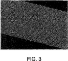
図1は、光射出面が前面つまり、ダイオードが構築される基板面の反対面である有機発光ダイオード(OLED)に関する。基板2の背面では、少なくとも一の第1型である陽極又は陰極の背面電極3を有する。背面電極3はまた、光学反射特性を有することで、射出面に向かって反射性となり、反射体を形成する。反射電極と呼ばれる背面電極3は金属的で、副次層を有することが可能な有機発光層4を上にする。有機発光層4は最終的には、規則的な周期配列をする突起パターンを有する エンボス加工した透明有機層5を上にする。そのパターンは、基本三角プリズム構造を形成する。このプリズム構造は、その前面が第2型である陰極又は陽極の実質的に透明な電極を支持する陰極又は陽極は第1型に従う。プリズム構造の面上では、この第2型電極は、不透明な領域7及び透明な取り出し領域とに分配される。前面電極は、OLED全面にわたって延在するのが好ましい。プリズム構造の端部は相互に平行である。ダイオード前面は、有機層中に作製されても良いし、又は透明有機層5を有する有機層上に付加されても良い。
FIG. 1 relates to an organic light emitting diode (OLED) in which the light exit surface is the front surface, that is, the opposite surface of the substrate surface on which the diode is built. The back surface of the
エンボス加工された層5は有機材料で構成されるのが好ましい。この有機材料では、ダイオードの電極間に印加される電位差を得るために適切なドーピングがなされることで、発光層領域全体でだいたい一定の電場が発生し、この領域を局所的に被覆する有機材料の厚さが如何なる厚さであろうとも。エンボス加工された層5はまた、たとえばPEDOT-PSS又はPANIのような導電性ポリマーで構成されても良い。このエンボス加工された層の表面は従って、一連の基本プリズムパターンを有する。そのプリズムパターンは、規則的に配備されているのが好ましく、発光有機層の全面にわたって長く延在するのが好ましい。
The embossed
第2型の全面電極6は二の層を有し:
有機層の突起パターンと適合しながらエンボス加工された有機層全面を被覆する、5nmのオーダーの厚さを有する非常に薄い導電性透明層;及び、
有機層の突起パターンと適合しながら不透明な反射領域7を形成し、これらの細片は従ってエンボス加工された有機層表面の一部のみを被覆する、500nmのオーダーの厚さを有する厚い金属細片;
を有する。
The second type
A very thin conductive transparent layer having a thickness on the order of 5 nm covering the entire embossed organic layer in conformity with the protrusion pattern of the organic layer; and
A thick metal strip with a thickness on the order of 500 nm, which forms an opaque
Have
OLEDの射出面は従って、反射細片及び、実質的に透明な細片の交互配置を有し、反射細片はまた良好な電気伝導性を有する。 The exit surface of the OLED thus has an alternating arrangement of reflective strips and substantially transparent strips, which also have good electrical conductivity.
有機発光層は、小さな分子、ポリマー、デンドリマー等で構成されて良い。又は、そのような材料を組み合わせたハイブリッド構造でも良い。有機層は、ドーピングはしても良いし、しなくても良い(蛍光及び/又は電気伝導のため)。有機発光層はまた、副次層を有しても良く、特に電荷つまり電子若しくは正孔を注入、輸送又は阻止する副次層を有しても良い。 The organic light emitting layer may be composed of small molecules, polymers, dendrimers and the like. Alternatively, a hybrid structure combining such materials may be used. The organic layer may or may not be doped (for fluorescence and / or electrical conduction). The organic light emitting layer may also have a sublayer, in particular a sublayer that injects, transports or blocks charges, ie electrons or holes.
上述の基本OLEDの製造する複数の態様(mode)は、それぞれ別なものと見なしても良いし、又は組み合わせと見なしても良い。態様には特に、前面電極3及び背面電極6の型、突起パターン形状、基本プリズム構造における取り出し領域及び反射領域の分布、各基本プリズム構造の形状及び長さ、取り出し面(基板面か否か)、基板面上に、任意でダイオード上の両面上に、突起パターンが存在するか否か、がある。全ての態様は組み合わせ可能である。
A plurality of modes (manufactured) of the basic OLED described above may be regarded as different from each other or may be regarded as a combination. In particular, the types of the
図1は、基本プリズム構造5上の反射第2層7の分布に関する第1態様を図示している。この態様において、反射領域は基本プリズム構造の同一平面(図1では左側の面)上に系統的に配備されているため、全てが互いに平行である。一定の基本プリズムパターンは、図1のOLEDの下向き斜視図である図3で見ることができるように繰り返されている。そのような態様では、二等辺三角形である(二の側面である、反射領域7と取り出し領域6とが実質的に同一の面を有する)基本プリズム構造の構造及び好適長さは、a=(底辺の幅)、b=(高さ)及び、α=(底辺と斜辺のなす角)として計算することによって決定された。よって以下の近似値が決定される。a=4μm、b=1.06μm及び、α=28°である。実際には、高さbは一般的にせいぜい2μm以下である。突起のこのように小さな厚さ(高さ)にすることで、多量の有機材料を使用せずに済むようにする。特に突起パターンを形成する透明有機層について言えば、この型の材料は特に高価である。
FIG. 1 illustrates a first aspect relating to the distribution of the reflective
上述の第1態様及び好適長さに従ったOLEDのシミュレーションから得られた結果は以下で与えられる。これらの結果は、有機層を真ん中にして、背中合わせに備えられた二のランベルト光源で構成される光源を使用し、初期光束Fini=1の発光をすることで得られる。平坦ガラス基板を上にする、有機層中の光源から構成される参照素子(参照OLED)は、取り出し利得を計算するために選択された。以下の量(任意単位)が、結果を示す表で与えられている。
RaL Alコーティングの反射係数
Io 通常観察(0°)での光強度
Fout 全放出光束
F15 15°のアパーチャの光錐における放出光束
F30 30°のアパーチャの光錐における放出光束
F45 45°のアパーチャの光錐における放出光束
The results obtained from the simulation of the OLED according to the first aspect and the preferred length described above are given below. These results are obtained by emitting light with an initial luminous flux F ini = 1 using a light source composed of two Lambert light sources provided back to back with the organic layer in the middle. A reference element (reference OLED) composed of a light source in an organic layer with a flat glass substrate on top was selected to calculate the extraction gain. The following quantities (in arbitrary units) are given in the table showing the results.
R aL Al coating reflection coefficient
Io Light intensity in normal observation (0 °)
Fout Total emission flux
F15 Emission flux in the light cone with 15 ° aperture
F30 Emission flux in the light cone with 30 ° aperture
F45 Emission flux in the light cone with 45 ° aperture

図2は、上述の、本発明の第1実施例に従ったOLEDの場合における反射細片7を堆積する態様を図示している。エンボス加工された有機層5での基本プリズム構造形成し、かつエンボス加工された有機層の全表面上に前面透明電極のうちの非常に薄い透明層を堆積した後、作製されたOLEDがチャンバ内に備えられる。そのチャンバでは、Alのような光学反射特性を有する金属をスパッタリング/スプレイによって堆積される。OLEDは、各基本プリズム構造の側面のみが当該金属で被覆されるように、金属のスパッタリング/スプレイ方向に対して傾いている。細片中で金属によって被覆されていない領域は前面電極の取り出し領域を形成する。
FIG. 2 illustrates the manner in which the
たとえ上述のOLEDが大幅な光取り出しの改善を可能にするとしても、図4から分かるように、この取り出しは、OLEDの射出面の法線に対してわずかにオフセット(25°)された平均方向で起こる。実際光強度は、OLED法線に対して約25°の観測角で最大となる。改良版では、従って、OLEDから取り出される光束を屈折させるプリズムを前面に備えることが提案されている。その屈折プリズムは、ダイオードの射出面に垂直な平均方向へ取り出し光を屈折させ、その屈折された光が進行する方向は一般に、ダイオードの一般面に垂直な平均方向に対応する。たとえ屈折手段が取り出し領域毎に供されることが可能だとしても(屈折手段の長さは基本プリズム構造の長さに近くなる)、OLEDの“画素”に対応する複数で一組の取り出し領域に作用する屈折手段を使用するのが好ましい。 Even though the OLED mentioned above allows for a significant improvement in light extraction, as can be seen from FIG. 4, this extraction is an average direction slightly offset (25 °) from the normal of the OLED exit surface. Happens at. The actual light intensity is maximum at an observation angle of about 25 ° relative to the OLED normal. In the improved version, it is therefore proposed to have a prism on the front side that refracts the light beam extracted from the OLED. The refractive prism refracts the extracted light in an average direction perpendicular to the exit surface of the diode, and the direction in which the refracted light travels generally corresponds to the average direction perpendicular to the general surface of the diode. Even if the refracting means can be provided for each extraction area (the length of the refracting means is close to the length of the basic prism structure), multiple sets of extraction areas corresponding to the “pixels” of the OLED It is preferable to use a refracting means acting on the surface.
この後者の場合、屈折手段は、長さ約300μm、幅約100μmのプリズムである。このプリズムのサイズは像ディスプレイユニットの画素の従来サイズに対応する。上述の屈折光を得るため、プリズムの高さは既知の方法で適合される。法線に対して25°傾いた平均放出方向を有する光錐を法線に沿って屈折させるため、図5Aで側面が図示されている屈折プリズムが使用される。この屈折プリズムは、屈折率n2が約1.5、角度Aが約35.45°の材料でできた直角三角形である。これらの値は、図5Bで図示されているように、空気中でのプリズムを考慮することで得られる。ここでOLED1(断面が図示されている)は、屈折率n1=1である大気中の光錐を自由空間8へ放出し、屈折プリズム9へ導光する。屈折プリズム9を介することで、OLEDによって25°傾いた方向に放出される光線が前方へ戻る。この例では、屈折プリズムは従って、屈折率n1=1である空気層によって、ダイオードの前面から隔てられている。シミュレーションによって得られた結果を以下に示す。
In this latter case, the refracting means is a prism having a length of about 300 μm and a width of about 100 μm. The prism size corresponds to the conventional size of the pixels of the image display unit. In order to obtain the above-mentioned refracted light, the height of the prism is adapted in a known manner. In order to refract a light cone having an average emission direction inclined by 25 ° with respect to the normal along the normal, a refracting prism whose side is illustrated in FIG. 5A is used. This refractive prism is a right triangle made of a material having a refractive index n 2 of about 1.5 and an angle A of about 35.45 °. These values are obtained by considering prisms in air, as illustrated in FIG. 5B. Here, the OLED 1 (the cross section is shown) emits a light cone in the atmosphere having a refractive index n 1 = 1 to the
図7は、基本プリズム構造5上での反射領域7の分布に関するOLED10の第2態様を図示している。この態様において、反射領域は対をなして、系統的に備えられている。対をなすとはつまり、二の隣接する反射細片の組み合わせをなしているということである。二の隣接反射細片は従って、二の隣接する基本プリズム構造の共通の底面に対応する共通の境界を有する。取り出し領域6もまた、図示されているように対で組み合わせられている。たとえ上述のように取り出し領域6及び反射領域7が異なるように、つまり対で備えられているとしても、一定の基本プリズムパターンは周期的に繰り返される。OLEDの側部終端では、OLEDの外向き面は、反射領域7を有するのが好ましい。それにもかかわらず、OLEDの全基本プリズム構造の数に従って、側部終端では、取り出し領域及び/又は、反射領域は他の構成を取ることが可能であることが分かるだろう。
FIG. 7 illustrates a second embodiment of the
そのような態様では、二等辺三角形(二の側面が実質的に同一の面を有する)である基本プリズム構造の構造及び好適長さは、a=(底辺の幅)、b=(高さ)及び、α=(底辺と斜辺のなす角)として計算することによって決定された。よって以下の近似値が決定される。a=4μm、b=1.4μm及び、α=35°である。実際には、高さbは一般的にせいぜい2μm以下である。 In such an embodiment, the structure and preferred length of the basic prism structure that is an isosceles triangle (the two side surfaces have substantially the same surface) are: a = (width of base), b = (height) And it was determined by calculating as α = (the angle between the base and the hypotenuse). Therefore, the following approximate value is determined. a = 4 μm, b = 1.4 μm, and α = 35 °. In practice, the height b is generally at most 2 μm or less.
上述の第2態様及び好適長さに従ったOLEDのシミュレーションから得られた結果は以下で与えられる。これらの結果は、有機層を真ん中にして、背中合わせに備えられた二のランベルト光源で構成される光源を使用し、初期光束Fini=1の発光をすることで得られる。平坦ガラス基板を上にする、有機層中の光源から構成される参照素子(参照OLED)は、取り出し利得を計算するために選択された。以下の量(任意単位)が、結果を示す表で与えられている。
RaL Alコーティングの反射係数
Io 通常観察(0°)での光強度
Fout 全放出光束
F15 15°のアパーチャの光錐における放出光束
F30 30°のアパーチャの光錐における放出光束
F60 60°のアパーチャの光錐における放出光束
The results obtained from the simulation of the OLED according to the second aspect and preferred length described above are given below. These results are obtained by emitting light with an initial luminous flux F ini = 1 using a light source composed of two Lambert light sources provided back to back with the organic layer in the middle. A reference element (reference OLED) composed of a light source in an organic layer with a flat glass substrate on top was selected to calculate the extraction gain. The following quantities (in arbitrary units) are given in the table showing the results.
R aL Al coating reflection coefficient
I o Light intensity in normal observation (0 °)
F out total luminous flux
F 15 Emission flux in the light cone with 15 ° aperture
F 30 Emission flux in a light cone with a 30 ° aperture
F 60 Emission flux in the light cone with 60 ° aperture
OLEDの射出光束の角度分布は図8で与えられる。ここで、放出エネルギーは法線で最大となり、ディスプレイ応用にとって都合の良い観察角度が増大するときに徐々に減少する。その減少は観察角度の向きに対して対称である。 The angular distribution of the OLED exit beam is given in FIG. Here, the emission energy is maximum at the normal and gradually decreases as the viewing angle, which is convenient for display applications, increases. The decrease is symmetric with respect to the viewing angle.
従来技術のOLEDsを製造する方法及び、それに使用される材料は、本発明に従ったOLEDsの製造に部分的に使用することが可能である。OLEDの前面及び/又は背面の製造はしかし、一方で基本プリズム構造を、他方で反射細片を得るため異なる。これらのプリズム構造では、エンボス加工技術を利用することが可能である。反射細片では、材料特に金属の違いをつけて堆積するための技術を利用することが可能である。 The method of manufacturing prior art OLEDs and the materials used therein can be used in part for the manufacture of OLEDs according to the present invention. The production of the front and / or back of the OLED, however, differs on the one hand to obtain a basic prism structure and on the other hand a reflective strip. With these prism structures, it is possible to use an embossing technique. Reflective strips can utilize techniques for depositing with different materials, especially metals.
OLEDの背面から前面にかけて、以下が存在する。 From the back to the front of the OLED, there are:
基板2は、使用される他の材料との相性が良く、光の上方取り出しに依存して、透明であっても、透明でなくても良い。考えられうる基板の例には、Si又は、特にアクティブマトリックスダイオードの場合ではプラスチック及びガラスがある。
The
基板上に備えられている反射背面電極3は金属的であることが好ましく、たとえばAl、Ag、Au、Cr、Cu又はこれらを含む合金で構成される。背面電極の型が陽極である場合、大きな仕事関数を有する、たとえばPt、Pd、NiCr等の材料で構成される付加的層は、高い導電性を有する第1金属層上に堆積されるのが好ましい。そのとき、背面電極は良好な反射率を有する。
The
有機発光材料からなる層4が引き続いて堆積される。副次層は材料内部で作製されて良い。これまでに堆積されてきた様々な層の厚さは均一であるため、平行な反対面を有する。 A layer 4 of organic luminescent material is subsequently deposited. The sublayer may be made inside the material. The various layers that have been deposited so far have a uniform thickness and thus have parallel opposite faces.
次に示されているように、エンボス加工された層5は、有機発光層4上に材料を付加することで作製されるのが好ましい。よって、エンボス加工された層を形成するため、n型(nドープ)透明有機材料が有機発光材料の層4上に堆積され、基本プリズム構造を形成するため、特にエンボス加工によって処理される。従ってエンボス加工された層5の厚さは均一ではない。その結果、他の種類の材料を排除することなく、エンボス加工された層を形成するためにドープされた有機透明材料は有利に、発光層4中で一定の電場を保証し、駆動電圧及びOLEDの発光の均一性を損なう欠陥の増大を回避することを可能にする。
As will be shown next, the embossed
実質的に透明な前面電極6が引き続いてエンボス加工された層5上に堆積される。陰極型の前面電極の場合において上述の堆積を実行するためには、電子のダイオードへの注入に使用するための、薄い(約0.1nm-5nm)、LiFのようなアルカリ金属フッ化物又はBaF2のようなアルカリ土類金属フッ化物等を有する電子注入副次層を、エンボス加工された層の全面に均一かつ規則的に堆積させる。さらに、Ca、Ybといった大きな仕事関数を有する材料からなる他の副次層(厚さは約5nm-20nmである)は、それまでのフッ化物等の堆積に関連して堆積されるだろう。電子注入副次層及び、小さな仕事関数を有する材料からなる他の副次層の代わりに、陰極を作製するために、たとえば金属材料又は、インジウムスズ酸化物ITO若しくはインジウム亜鉛酸化物IZOのような透明導電性酸化物他の透明導電性材料を検討することも可能である。
A substantially transparent
最終的には、一以上の反射導電性細片7が引き続いて、基本プリズム構造の選択面上に作製される。選択面は選択された実施例に依存する(図1、図7又は他の実施例)。上述のように、たとえばAl、Ag、Au、Cr又はこれらを含む合金の金属層を堆積させることが可能である。これらの層の厚さは、所望の反射特性及び伝導特性を得るのに十分な厚さである。
Eventually, one or more reflective
OLED内部で電極の型が入れ替わる場合、大きな/小さな仕事関数を有する材料からなる付加層も入れ替わり、付加層が用いられる場合には、エンボス加工された層は、p型(pドープ)有機材料を堆積することで得られる。 When the electrode type is switched inside the OLED, the additional layer made of a material having a large / small work function is also switched. When the additional layer is used, the embossed layer is made of p-type (p-doped) organic material. It is obtained by depositing.
OLEDの有機材料内部で発生し、取り出し領域へ向かって導光される光はOLEDをそのまま直進する。他の方向ではそれとは対称的に、光は、反射性背面電極3及び、前面電極の反射細片7(反射領域)によって反射され、前面電極の取り出し領域へ向かうことが可能である。背面電極3と反射細片7とは平行ではないことに留意すべきである。OLED内部で発生する全ての光は擬似的に(材料の再吸収及び不完全性を無視する)、透明前面電極の取り出し領域を介することでOLEDからの取り出しが可能となる。
Light generated inside the organic material of the OLED and guided toward the extraction area goes straight through the OLED. Symmetrically in the other direction, light can be reflected by the
これまで与えられてきた典型的実施例は、実質的に透明な電極の透明取り出し領域及び反射領域が、一定の厚さを有する、繰り返し構造でかつ相互に平行な細長い細片である、取り出し細片及び反射細片をそれぞれ形成するダイオードに関する。取り出し細片及び反射細片はプリズム構造を形成するので、同一平面上にはない。第3実施例では、取り出し領域と反射領域とを同一平面上に設けることで本発明を実装することが可能である。ただし、反射領域は平面ではなく突起を有する。これらの突起は、直接反射又は多重反射によって、当該層へ、発生し、取り出し領域を透過しない光線を反射させることが可能なように、有機発光層へ向かって凸の反射性半球構造に対応する。よってこれらの光線は、実質的に透明な電極から反対側にある反射体(たとえば反射陰極)に到達することで戻ることが可能である。これらの突起自体は、突起の半球部分、つまり内向きに曲がっている光路、が有機発光層に向いている限り、半球又は球(完全球)であって良い。これらの突起は従って、少なくとも当該層及び突起に電球が流れるようにし、ダイオードの構造的安定性を保証するため、反射領域の導電性反射層に関連し、同一の金属材料又は少なくとも相性の良い材料で構成されるのが好ましい。 The exemplary embodiment given so far is that the transparent extraction and reflection areas of the substantially transparent electrode are elongate strips of repetitive structure and parallel to each other having a constant thickness. The present invention relates to a diode that forms a strip and a reflective strip, respectively. Since the extraction strip and the reflection strip form a prism structure, they are not on the same plane. In the third embodiment, the present invention can be implemented by providing the extraction region and the reflection region on the same plane. However, the reflection region has a protrusion instead of a flat surface. These protrusions correspond to a reflective hemispherical structure that is convex toward the organic light emitting layer so that it can reflect light rays that are generated by direct reflection or multiple reflection to the layer and do not pass through the extraction region. . Thus, these rays can be returned by reaching a reflector (eg, a reflective cathode) on the opposite side from the substantially transparent electrode. These protrusions themselves may be hemispheres or spheres (perfect spheres) as long as the hemispherical portion of the protrusions, i.e. the inwardly bent optical path, is towards the organic light emitting layer. These protrusions are therefore associated with the conductive reflective layer in the reflective region, at least in order to allow the bulb to flow through the layer and the protrusion, and to ensure the structural stability of the diode, the same metallic material or at least compatible material It is preferable that it is comprised.
図9は、相互に隣接する整列した球状突起の列を有する反射細片による第3実施例を特別な実装態様を図示している。突起は同一直径Dを有する。各反射細片つまり導電性反射細片の幅は、突起の直径に対応する。 FIG. 9 illustrates a special implementation of the third embodiment with reflective strips having rows of aligned spherical protrusions adjacent to each other. The protrusions have the same diameter D. The width of each reflective strip or conductive reflective strip corresponds to the diameter of the protrusion.
図10は、図9のダイオードの概略的上面図である。この概略図は、透明取り出し細片(実質的に透明な導電層)及び、反射細片(実質的に透明な導電層に対する導電性反射層)の幅の決定を可能にするための数値シミュレーションを実行するためである。 FIG. 10 is a schematic top view of the diode of FIG. This schematic shows a numerical simulation to allow determination of the width of the transparent strip (substantially transparent conductive layer) and the reflective strip (conductive reflective layer relative to the substantially transparent conductive layer). This is to execute.
図11のダイオードは、たとえばガラス、Si又は他の相性の良い材料のような基板2上で製造される。反射体を形成するため、実質的に均一な厚さの反射性の金属背面電極3は基板2上に備えられている。この背面電極3上に、実質的に均一な厚さの有機発光層4(副次層を有することが好ましい)が設けられる。有機発光層4上に堆積させることで、実質的に厚い、ドープされた有機材料層5又は導電性ポリマー層が存在し、透明でかつ導電性の有機層が形成される。その有機層の厚さは位置によって変化し、取り出し領域8(この例では細片)及び反射領域7を有する、実質的に透明な電極(前面電極)がその有機層の上になる。実質的に透明な電極の取り出し領域8は、実質的に透明な導電層11によって形成される。実質的に透明な導電層はたとえば、これまでの例で紹介してきたように、金属、ITO又はLiF-Caである。実質的に透明な電極の反射領域7は、実質的に透明な導電層11の上にある反射球(発光効率を増大させるために相互に隣接しているのが好ましい)を有する反射導電層12によって形成される。図11で図示されているように、実質的に透明な導電層は連続的である。たとえばSiO又はSiO2のような透明被覆層13は、集合体を保護することができる。
The diode of FIG. 11 is fabricated on a
そのようなダイオードを製造するため、背面電極3、有機発光層4、ドープされた透明有機層5及び実質的に透明な導電層11を基板2上に有する、従来技術での作製が可能な構造を作製するために、以下の手順を使用することが可能である。感光性樹脂層を実質的に透明な導電層11上に堆積させ、マスク及び露光によって樹脂を除去することで、厚さ数μmの一連の細片が作製される。樹脂のないこれらの細片は反射領域に対応する。直径数μmの金属球が、これらの細片に堆積され、その金属球の直径の約10%-50%の直径が当該構造に湾入されるように、構造に対して押しつけられる。金属(たとえばAl、Crなど)が続いて堆積され、他の導電性反射層を形成し、所与の反射細片の球と電気的に接続し、樹脂は堆積された金属の他の部分と一緒に除去される。ダイオードを密閉するため、SiO、SiO2などの透明被覆層13が続いて堆積される。あるいはその代わりに、半球状パターンを有するテンプレートをエンボス加工することで、細片中の構造の表面を変化させる半球状パターンを有するそのようなダイオードを作製することが可能である。細片では、樹脂が除去されている。その構造の表面は、少なくとも部分的には半球状のくぼみを有する(半球の20%から100%)。その半球状のくぼみは、導電性反射層を形成するため、金属堆積中に満たされる。
In order to produce such a diode, it has a
この第3実施例に従ったダイオードを最適化するため、ソフトウエアASAP(登録商標)を使用したシミュレーションが実行された。導電性反射層の突起が取り得る全形状の中で、球(又は少なくとも半球)が最も効率的であることが示された。互いに隣接する球からなる単一線を有する細片の場合、最適光取り出し効率(EFF)は、取り出し領域の全表面とダイオードの領域との間の効率/比から決定することが可能である(ダイオードの領域とは、取り出し領域の全表面と反射領域の全表面との和である)。曲線EFF/OAR1は図12に図示されている。最大光効率については、比OAR1は、40%-70%の範囲であり、約53%が好ましい。比OAR1がこの範囲の値に留まっているときには、取り出し効率EFFは、ほとんど変化しないのが観察される。本発明に従った取り出し手段は従って、比OAR1を変化させる恐れのある、製造方法でのばらつきにそれほど敏感ではないという利点を有する。しかし、所与の比(OAR1)における取り出し及び反射細片の幅が任意のため、細片の幅もまた、シミュレーションによる最適化過程によって決定することが可能である。図13に図示された曲線は、取り出し細片と反射細片との幅の比(OAR2)の関数として取り出し効率(EFF)を与えている。各細片の幅は、これまでに決定された最適値に対応する所与の値OAR1での幅である。細片幅の最適比は、0.75-0.85であり、取り出し細片(領域)は反射細片(領域)よりも広くする必要があることが分かった。そのような場合(等方性光源を仮定する)では、取り出し利得Gは、0.26/0.17つまり53%となる。 In order to optimize the diode according to this third embodiment, a simulation using the software ASAP® was performed. Of all the shapes that the projections of the conductive reflective layer can take, spheres (or at least hemispheres) have been shown to be the most efficient. For strips with a single line of adjacent spheres, the optimal light extraction efficiency (EFF) can be determined from the efficiency / ratio between the entire surface of the extraction region and the region of the diode (diode). Is the sum of the entire surface of the extraction region and the entire surface of the reflection region). Curve EFF / OAR1 is illustrated in FIG. For maximum light efficiency, the ratio OAR1 is in the range of 40% -70%, preferably about 53%. When the ratio OAR1 remains within this range, it is observed that the extraction efficiency EFF hardly changes. The take-out means according to the invention thus has the advantage that it is not very sensitive to variations in the manufacturing method, which can change the ratio OAR1. However, since the extraction and reflection strip widths at a given ratio (OAR1) are arbitrary, the strip width can also be determined by an optimization process through simulation. The curve shown in FIG. 13 gives the extraction efficiency (EFF) as a function of the width ratio (OAR2) between the extraction strip and the reflection strip. The width of each strip is the width at a given value OAR1 corresponding to the optimum value determined so far. The optimum strip width ratio was 0.75-0.85, and it was found that the removal strip (region) should be wider than the reflective strip (region). In such a case (assuming an isotropic light source), the extraction gain G is 0.26 / 0.17 or 53%.
上述の例は本発明を限定するものではなく、本発明の技術範囲内で他の代替例が考えられ得る。特に、たとえ、実質的に平面だが、両領域間にプリズム構造を形成する取り出し領域及び反射領域、又は、同一面上だが、反射領域は突起が有している取り出し領域及び反射領域が好適実施例において検討されたとしても、両領域のうちの一又は両方を曲げ、この形状を利用して、より特殊な光学効果を得ることも考えられ得る(たとえばダイオード内側へ向かって放物面、及び/又はダイオード外側へ向かって放物面となるようなミラー)。特にエンボス加工のような、使用される技術により、より単純に、前面及び/又は背面の特定形状を得ることが可能となる。さらに、電極(反射金属は良好な導体である)であることが好適であるとして説明してきた反射背面層3は、背面電極にたいして独立して良い。同様に、基板それ自体が反射性の場合、背面反射層は省略可能である。同様に、反射層は、単一種類の金属を堆積させるよりは、誘電層の積層構造(誘電ミラー)を実装することで製造して良い。
The above examples do not limit the invention and other alternatives are conceivable within the scope of the invention. In particular, the extraction area and the reflection area which are substantially planar but form a prism structure between the two areas, or the extraction area and the reflection area which are on the same surface but have the projections are preferred embodiments. May be considered to bend one or both of both regions and take advantage of this shape to obtain more specific optical effects (eg, paraboloids towards the inside of the diode, and / or Or a mirror that forms a paraboloid toward the outside of the diode). The technique used, in particular embossing, makes it possible to obtain a simpler front and / or back specific shape more simply. Furthermore, the
Claims (13)
前記電極を介して流れる電流によって前記有機発光層に正孔及び電子が注入されるときに前記有機発光層が光を発生させ、
前記電極の型は陽極と陰極に対応し、前記発生光が、射出面と呼ばれる前記ダイオードの面のうちの一面を介して外へ飛び出すことができるように、前記電極のうちの少なくとも一は、前記発生光に対して実質的に透明で、
前記実質的に透明な電極は、少なくとも一の透明取り出し領域及び、前記発光層を介することで前記発生光を戻すための少なくとも一の反射領域を有し、
前記ダイオードはまた、前記有機発光層からみて前記の実質的に透明な電極の反対側に備えられていて、前記発光層を介して前記の実質的に透明な電極へ前記発生光を戻す反射体を有し、
前記発生光の取り出し領域及び反射領域を有する前記の実質的に透明な電極によって形成される表面は、前記の反射体によって形成される表面とは平行とはならず、
前記反射体、並びに、前記の取り出し領域及び反射領域を有する実質的に透明な電極のうちのいずれか一又は両方が、少なくとも一の突起パターン上に存在し、
前記有機発光層と前記電極のいずれか一との間に、前記電極を支持し、前記突起パターンを形成し、かつ位置によって厚さが変化する透明有機層を有し、
電荷の輸送、つまり電子又は正孔の輸送を可能にするため、前記透明有機層がドープされていることを特徴とする有機発光ダイオード(OLED)。From the back side of the substrate to the front side, the organic light emitting layer is provided on at least one so-called first type back electrode, and at least one so-called second type front electrode on the organic light emitting layer,
The organic light emitting layer generates light when holes and electrons are injected into the organic light emitting layer by a current flowing through the electrode,
The electrode type corresponds to an anode and a cathode, and at least one of the electrodes is such that the generated light can jump out through one of the surfaces of the diode called the exit surface. Substantially transparent to the generated light,
The substantially transparent electrode has at least one transparent extraction region and at least one reflection region for returning the generated light through the light emitting layer,
The diode is also provided on the opposite side of the substantially transparent electrode as viewed from the organic light emitting layer, and returns the generated light to the substantially transparent electrode through the light emitting layer. Have
The surface formed by the substantially transparent electrode having the generated light extraction region and the reflection region is not parallel to the surface formed by the reflector,
Any one or both of the reflector and the substantially transparent electrode having the extraction region and the reflection region are present on at least one protrusion pattern;
Between the organic light emitting layer and any one of the electrodes, a transparent organic layer that supports the electrode, forms the protrusion pattern, and has a thickness that varies depending on the position,
An organic light emitting diode (OLED), characterized in that the transparent organic layer is doped in order to allow charge transport, ie transport of electrons or holes.
前記反射領域及び前記取り出し領域の両方に延在する実質的に透明な導電層;及び、
前記反射領域にのみ延在する、前記透明導電層上に設けられている導電性反射層;
を有することを特徴とする、請求項1又は2に記載の有機発光ダイオード(OLED)。A substantially transparent electrode having the extraction region and the reflective region is:
A substantially transparent conductive layer extending to both the reflective region and the extraction region; and
A conductive reflective layer provided on the transparent conductive layer, extending only to the reflective region;
The organic light-emitting diode (OLED) according to claim 1 or 2, characterized by comprising:
前記の実質的に透明な電極上で、前記反射領域が、前記取り出し領域に対して相補的である、
ことを特徴とする、請求項1から3のうちのいずれか1つに記載の有機発光ダイオード(OLED)。The generated light is emitted from the OLED through a set of more than one extraction region, and
On the substantially transparent electrode, the reflective region is complementary to the extraction region;
An organic light emitting diode (OLED) according to any one of claims 1 to 3, characterized in that
反射電極と呼ばれる、もう一方の電極が反射性で、かつ前記反射体を形成する、
ことを特徴とする、請求項1から4のうちのいずれか1つに記載の有機発光ダイオード(OLED)。Only one of the electrodes is substantially transparent,
The other electrode, called the reflective electrode, is reflective and forms the reflector,
An organic light emitting diode (OLED) according to any one of claims 1 to 4, characterized in that.
前記の実質的に透明な電極における透明取り出し領域及び反射領域の各々が実質的に平面で、前記反射電極に対して傾いていて、
その結果、前記領域が少なくとも一の基本三角プリズム構造を形成し、前記プリズムの3辺が実質的に前記反射電極と平行である、
ことを特徴とする、請求項6に記載の有機発光ダイオード(OLED)。The reflective electrode is substantially planar;
Each of the transparent extraction region and the reflective region in the substantially transparent electrode is substantially planar and inclined with respect to the reflective electrode;
As a result, the region forms at least one basic triangular prism structure, and the three sides of the prism are substantially parallel to the reflective electrode.
7. The organic light emitting diode (OLED) according to claim 6, wherein the organic light emitting diode is an organic light emitting diode (OLED).
前記各取り出し領域は反射領域によって隣の取り出し領域と隔てられ、
前記取り出し領域は相互に平行で、
前記反射領域は相互に平行で、
前記の取り出し領域及び反射領域が、前記基本三角プリズム構造の規則的周期構造に従って、前記の実質的に透明な電極上に配備されている、
ことを特徴とする、請求項7に記載の有機発光ダイオード(OLED)。The light is emitted from the OLED through a set of more than one extraction area;
Each extraction region is separated from the adjacent extraction region by a reflective region;
The extraction areas are parallel to each other,
The reflective areas are parallel to each other;
The extraction region and the reflection region are disposed on the substantially transparent electrode according to a regular periodic structure of the basic triangular prism structure;
8. The organic light emitting diode (OLED) according to claim 7, characterized in that.
前記の対をなす二の取り出し領域は相互に隣接し、共通の底面を有し、
前記の対をなす二の取り出し領域は、対をなす相互に隣接して共通の底辺を有する反射領域によって隣の対をなす取り出し領域と隔てられ、
前記の取り出し領域及び反射領域の対が、前記基本三角プリズム構造の規則的周期構造に従って、前記実質的に透明な電極上に配備されている、
ことを特徴とする、請求項7に記載の有機発光ダイオード(OLED)。The light is emitted from the OLED through a set of more than one extraction region that forms a group in pairs;
The two paired extraction regions are adjacent to each other and have a common bottom surface;
The pair of extraction regions are separated from the adjacent extraction region by a reflective region having a common base adjacent to each other in a pair;
The extraction region and reflection region pairs are disposed on the substantially transparent electrode according to a regular periodic structure of the basic triangular prism structure;
8. The organic light emitting diode (OLED) according to claim 7, characterized in that.
前記突起は少なくとも、前記有機層に向かって凸で、かつ直径Dを有する反射性半球または球であって、
前記の少なくとも半球の突起は相互に整列し、各反射細片に沿って接し、
各反射細片の幅は、n≧1とするとnDである、
ことを特徴とする、請求項6に記載の有機発光ダイオード(OLED)。The reflective strip has a protrusion;
The protrusion is at least a reflective hemisphere or sphere convex toward the organic layer and having a diameter D;
The at least hemispherical protrusions are aligned with each other and touching along each reflective strip;
The width of each reflective strip is nD when n ≧ 1,
7. The organic light emitting diode (OLED) according to claim 6, wherein the organic light emitting diode is an organic light emitting diode (OLED).
前記ダイオードにおける、前記のダイオード領域に対する前記の取り出し領域の全表面の比が、40%から70%である、
ことを特徴とする、請求項11に記載の有機発光ダイオード(OLED)。The area of the diode is the sum of the entire surface of the extraction area and the entire surface of the reflection area,
In the diode, the ratio of the entire surface of the extraction region to the diode region is 40% to 70%.
12. The organic light emitting diode (OLED) according to claim 11, characterized in that.
Applications Claiming Priority (3)
| Application Number | Priority Date | Filing Date | Title |
|---|---|---|---|
| FR0450956 | 2004-05-17 | ||
| FR0450956 | 2004-05-17 | ||
| PCT/FR2005/050322 WO2005114762A1 (en) | 2004-05-17 | 2005-05-13 | Organic light-emitting diode (oled) with improved light extraction and corresponding display unit |
Publications (2)
| Publication Number | Publication Date |
|---|---|
| JP2007538363A JP2007538363A (en) | 2007-12-27 |
| JP4806678B2 true JP4806678B2 (en) | 2011-11-02 |
Family
ID=34945683
Family Applications (1)
| Application Number | Title | Priority Date | Filing Date |
|---|---|---|---|
| JP2007517373A Expired - Fee Related JP4806678B2 (en) | 2004-05-17 | 2005-05-13 | Organic light emitting diode (OLED) with improved light extraction and corresponding display unit |
Country Status (6)
| Country | Link |
|---|---|
| US (1) | US7733011B2 (en) |
| EP (1) | EP1766703A1 (en) |
| JP (1) | JP4806678B2 (en) |
| KR (1) | KR101201928B1 (en) |
| CN (1) | CN100555705C (en) |
| WO (1) | WO2005114762A1 (en) |
Families Citing this family (37)
| Publication number | Priority date | Publication date | Assignee | Title |
|---|---|---|---|---|
| DE102005034873B4 (en) * | 2005-07-26 | 2013-03-07 | Siemens Aktiengesellschaft | Arrangement of an electrical component and a laminated on the component film composite and method for producing the assembly |
| US7498735B2 (en) | 2005-10-18 | 2009-03-03 | Eastman Kodak Company | OLED device having improved power distribution |
| US8884322B2 (en) | 2006-09-22 | 2014-11-11 | Osram Opto Semiconductor Gmbh | Light-emitting device |
| DE102006052029B4 (en) * | 2006-09-22 | 2020-01-09 | Osram Oled Gmbh | Light emitting device |
| JP2010512662A (en) | 2006-12-11 | 2010-04-22 | ザ リージェンツ オブ ザ ユニバーシティ オブ カリフォルニア | Transparent light emitting diode |
| JP2008234922A (en) * | 2007-03-19 | 2008-10-02 | Seiko Epson Corp | Organic EL device, line head, and electronic device |
| US8179034B2 (en) | 2007-07-13 | 2012-05-15 | 3M Innovative Properties Company | Light extraction film for organic light emitting diode display and lighting devices |
| DE102007059732B4 (en) * | 2007-12-12 | 2020-11-12 | Pictiva Displays International Limited | Light emitting device |
| KR100970482B1 (en) * | 2008-12-04 | 2010-07-16 | 삼성전자주식회사 | Organic light emitting device and manufacturing method |
| WO2010066245A1 (en) * | 2008-12-11 | 2010-06-17 | Osram Opto Semiconductors Gmbh | Organic light-emitting diode and luminaire |
| CN101783395A (en) * | 2009-01-20 | 2010-07-21 | 京东方科技集团股份有限公司 | Organic electroluminescence component and manufacturing method thereof |
| KR101613865B1 (en) * | 2009-03-26 | 2016-04-20 | 가부시키가이샤 한도오따이 에네루기 켄큐쇼 | Light-emitting device and method for manufacturing the same |
| US8981397B2 (en) | 2010-02-12 | 2015-03-17 | Tsmc Solid State Lighting Ltd. | Light-emitting devices on textured substrates |
| KR101055003B1 (en) * | 2010-03-09 | 2011-08-05 | 엘지이노텍 주식회사 | Light emitting device, light emitting device package, lighting system, and light emitting device manufacturing method |
| EP2383817A1 (en) | 2010-04-29 | 2011-11-02 | Nederlandse Organisatie voor toegepast -natuurwetenschappelijk onderzoek TNO | Light-emitting device and method for manufacturing the same |
| KR101797095B1 (en) | 2010-09-29 | 2017-12-13 | 삼성디스플레이 주식회사 | Organic light emitting display device and manufacturing method of the same |
| EP2630679B1 (en) * | 2010-10-20 | 2015-03-18 | Koninklijke Philips N.V. | Organic electroluminescent device. |
| JP6235475B2 (en) * | 2011-10-28 | 2017-11-22 | コーニンクレッカ フィリップス エヌ ヴェKoninklijke Philips N.V. | Transparent OLED device with structured cathode and method for manufacturing such OLED device |
| WO2013065177A1 (en) * | 2011-11-04 | 2013-05-10 | パイオニア株式会社 | Light-emitting device |
| JPWO2013065177A1 (en) * | 2011-11-04 | 2015-04-02 | パイオニア株式会社 | Light emitting device |
| WO2013065170A1 (en) * | 2011-11-04 | 2013-05-10 | パイオニア株式会社 | Light-emitting device |
| WO2013065178A1 (en) * | 2011-11-04 | 2013-05-10 | パイオニア株式会社 | Light-emitting device |
| WO2013065172A1 (en) * | 2011-11-04 | 2013-05-10 | パイオニア株式会社 | Light-emitting device and method for producing light-emitting device |
| CN103280536A (en) * | 2012-08-24 | 2013-09-04 | 厦门天马微电子有限公司 | Top-transmitting type active matrix organic light emitting display |
| JP5723344B2 (en) | 2012-09-25 | 2015-05-27 | 株式会社東芝 | Organic electroluminescent device and light emitting device |
| TW201423527A (en) * | 2012-12-13 | 2014-06-16 | Subtron Technology Co Ltd | Optical touch sensing structure |
| WO2014103043A1 (en) * | 2012-12-28 | 2014-07-03 | パイオニア株式会社 | Light-emitting device |
| WO2014103041A1 (en) * | 2012-12-28 | 2014-07-03 | パイオニア株式会社 | Light-emitting device |
| WO2014103042A1 (en) * | 2012-12-28 | 2014-07-03 | パイオニア株式会社 | Light-emitting device |
| US20140241731A1 (en) * | 2013-02-28 | 2014-08-28 | Harris Corporation | System and method for free space optical communication beam acquisition |
| CN104576703B (en) * | 2015-01-22 | 2017-07-04 | 京东方科技集团股份有限公司 | Array base palte, display panel and display device |
| CN107170904B (en) | 2017-06-30 | 2019-10-15 | 京东方科技集团股份有限公司 | OLED display substrate, method for making the same, and display device |
| EP3493287B1 (en) | 2017-12-01 | 2022-11-23 | InterDigital Madison Patent Holdings, SAS | An organic light emitting diode cell comprising a set of right circular hollow cylinders |
| US10964905B2 (en) | 2019-04-08 | 2021-03-30 | Interdigital Ce Patent Holdings | Organic light emitting diode cell comprising a set of right circular hollow cylinders |
| US11592166B2 (en) | 2020-05-12 | 2023-02-28 | Feit Electric Company, Inc. | Light emitting device having improved illumination and manufacturing flexibility |
| US11876042B2 (en) | 2020-08-03 | 2024-01-16 | Feit Electric Company, Inc. | Omnidirectional flexible light emitting device |
| CN115408764B (en) * | 2022-11-01 | 2023-03-24 | 江西立盾光电科技有限公司 | Arrangement method and system of indoor LED lamps |
Citations (8)
| Publication number | Priority date | Publication date | Assignee | Title |
|---|---|---|---|---|
| EP0442002A1 (en) * | 1990-02-13 | 1991-08-21 | Siemens Aktiengesellschaft | Radiation producing semiconductor device |
| JPH0682771A (en) * | 1991-12-31 | 1994-03-25 | American Teleph & Telegr Co <Att> | Transparent display device and manufacture thereof |
| JPH0963767A (en) * | 1995-08-18 | 1997-03-07 | Sumitomo Chem Co Ltd | Organic electroluminescence device |
| JPH10308284A (en) * | 1997-05-08 | 1998-11-17 | Idemitsu Kosan Co Ltd | Organic electroluminescence device |
| JP2001085163A (en) * | 1999-09-20 | 2001-03-30 | Sony Corp | Organic electroluminescence element, method of manufacturing the same, and display device |
| JP2003036969A (en) * | 2000-10-25 | 2003-02-07 | Matsushita Electric Ind Co Ltd | Light emitting device, and display device and lighting device using the same |
| US20030117067A1 (en) * | 2001-12-21 | 2003-06-26 | Daniel B. Roitman | OLED having improved light extraction efficiency |
| JP2003317970A (en) * | 2002-04-25 | 2003-11-07 | Dainippon Printing Co Ltd | Spherical organic EL device |
Family Cites Families (12)
| Publication number | Priority date | Publication date | Assignee | Title |
|---|---|---|---|---|
| US5349503A (en) * | 1991-12-31 | 1994-09-20 | At&T Bell Laboratories | Illuminated transparent display with microtextured back reflector |
| US6046543A (en) | 1996-12-23 | 2000-04-04 | The Trustees Of Princeton University | High reliability, high efficiency, integratable organic light emitting devices and methods of producing same |
| JP2000231985A (en) * | 1999-02-12 | 2000-08-22 | Denso Corp | Organic EL device |
| JP4136185B2 (en) * | 1999-05-12 | 2008-08-20 | パイオニア株式会社 | Organic electroluminescent multicolor display and method for manufacturing the same |
| JP4434411B2 (en) * | 2000-02-16 | 2010-03-17 | 出光興産株式会社 | Active drive type organic EL light emitting device and manufacturing method thereof |
| TW527848B (en) * | 2000-10-25 | 2003-04-11 | Matsushita Electric Industrial Co Ltd | Light-emitting element and display device and lighting device utilizing thereof |
| CN1138175C (en) * | 2001-06-21 | 2004-02-11 | 胜华科技股份有限公司 | Light guide structure of liquid crystal display |
| JP4152665B2 (en) * | 2001-07-11 | 2008-09-17 | 株式会社半導体エネルギー研究所 | Light emitting device and manufacturing method thereof |
| KR100437886B1 (en) * | 2001-09-25 | 2004-06-30 | 한국과학기술원 | High extraction efficiency photonic crystal organic light emitting device |
| US6812637B2 (en) * | 2003-03-13 | 2004-11-02 | Eastman Kodak Company | OLED display with auxiliary electrode |
| US20070069642A1 (en) * | 2003-09-05 | 2007-03-29 | Adrian Kitai | Sphere-supported thin film phosphor electroluminescent devices |
| JP4165478B2 (en) * | 2003-11-07 | 2008-10-15 | セイコーエプソン株式会社 | LIGHT EMITTING DEVICE AND ELECTRONIC DEVICE |
-
2005
- 2005-05-13 JP JP2007517373A patent/JP4806678B2/en not_active Expired - Fee Related
- 2005-05-13 US US11/596,749 patent/US7733011B2/en not_active Expired - Fee Related
- 2005-05-13 CN CNB2005800196923A patent/CN100555705C/en not_active Expired - Fee Related
- 2005-05-13 KR KR1020067023945A patent/KR101201928B1/en not_active Expired - Fee Related
- 2005-05-13 EP EP05762550A patent/EP1766703A1/en not_active Withdrawn
- 2005-05-13 WO PCT/FR2005/050322 patent/WO2005114762A1/en not_active Ceased
Patent Citations (8)
| Publication number | Priority date | Publication date | Assignee | Title |
|---|---|---|---|---|
| EP0442002A1 (en) * | 1990-02-13 | 1991-08-21 | Siemens Aktiengesellschaft | Radiation producing semiconductor device |
| JPH0682771A (en) * | 1991-12-31 | 1994-03-25 | American Teleph & Telegr Co <Att> | Transparent display device and manufacture thereof |
| JPH0963767A (en) * | 1995-08-18 | 1997-03-07 | Sumitomo Chem Co Ltd | Organic electroluminescence device |
| JPH10308284A (en) * | 1997-05-08 | 1998-11-17 | Idemitsu Kosan Co Ltd | Organic electroluminescence device |
| JP2001085163A (en) * | 1999-09-20 | 2001-03-30 | Sony Corp | Organic electroluminescence element, method of manufacturing the same, and display device |
| JP2003036969A (en) * | 2000-10-25 | 2003-02-07 | Matsushita Electric Ind Co Ltd | Light emitting device, and display device and lighting device using the same |
| US20030117067A1 (en) * | 2001-12-21 | 2003-06-26 | Daniel B. Roitman | OLED having improved light extraction efficiency |
| JP2003317970A (en) * | 2002-04-25 | 2003-11-07 | Dainippon Printing Co Ltd | Spherical organic EL device |
Also Published As
| Publication number | Publication date |
|---|---|
| CN1969405A (en) | 2007-05-23 |
| US20090072711A1 (en) | 2009-03-19 |
| JP2007538363A (en) | 2007-12-27 |
| EP1766703A1 (en) | 2007-03-28 |
| CN100555705C (en) | 2009-10-28 |
| KR101201928B1 (en) | 2012-11-16 |
| WO2005114762A1 (en) | 2005-12-01 |
| US7733011B2 (en) | 2010-06-08 |
| KR20070012484A (en) | 2007-01-25 |
Similar Documents
| Publication | Publication Date | Title |
|---|---|---|
| JP4806678B2 (en) | Organic light emitting diode (OLED) with improved light extraction and corresponding display unit | |
| US11832474B2 (en) | OLED device having enhancement layer(s) | |
| US8987767B2 (en) | Light emitting device having improved light extraction efficiency | |
| US20070201234A1 (en) | Luminous element | |
| US20070096112A1 (en) | Area light emitting device | |
| JP2012204103A (en) | Organic electroluminescent element, display device and luminaire | |
| KR20100111685A (en) | Light-emitting device | |
| KR20080010458A (en) | Full length luminous source | |
| WO2010128439A1 (en) | Electroluminescent device | |
| KR20180125018A (en) | Patterned organic light emitting diodes (OLEDs) with enhanced light extraction | |
| TWI415297B (en) | Optoelectronic semiconductor wafer | |
| JP6171317B2 (en) | Surface emitting unit | |
| JP5495704B2 (en) | LIGHT EMITTING ELEMENT AND MANUFACTURING METHOD THEREOF | |
| CN105474423A (en) | Radiation-emitting apparatus | |
| JPS6391998A (en) | El light emission array | |
| US20120091434A1 (en) | Vertical light-emitting device | |
| CN103918348A (en) | Light-emitting device | |
| US20160327231A1 (en) | Surface-Emitting Unit | |
| JP2003168553A (en) | Organic LED element | |
| CN104937738B (en) | Lighting modules with optimized light output | |
| KR102080774B1 (en) | A light emitting device | |
| JP2012104739A (en) | Light-emitting element | |
| US11690249B2 (en) | Light extraction substrate of organic light-emitting device and method of fabricating the same | |
| JP6528513B2 (en) | Surface emitting module | |
| JP6414468B2 (en) | Surface emitting unit |
Legal Events
| Date | Code | Title | Description |
|---|---|---|---|
| A621 | Written request for application examination |
Free format text: JAPANESE INTERMEDIATE CODE: A621 Effective date: 20080417 |
|
| A131 | Notification of reasons for refusal |
Free format text: JAPANESE INTERMEDIATE CODE: A131 Effective date: 20100727 |
|
| A521 | Request for written amendment filed |
Free format text: JAPANESE INTERMEDIATE CODE: A523 Effective date: 20101026 |
|
| A131 | Notification of reasons for refusal |
Free format text: JAPANESE INTERMEDIATE CODE: A131 Effective date: 20101124 |
|
| A521 | Request for written amendment filed |
Free format text: JAPANESE INTERMEDIATE CODE: A523 Effective date: 20110216 |
|
| A131 | Notification of reasons for refusal |
Free format text: JAPANESE INTERMEDIATE CODE: A131 Effective date: 20110405 |
|
| A521 | Request for written amendment filed |
Free format text: JAPANESE INTERMEDIATE CODE: A523 Effective date: 20110704 |
|
| TRDD | Decision of grant or rejection written | ||
| A01 | Written decision to grant a patent or to grant a registration (utility model) |
Free format text: JAPANESE INTERMEDIATE CODE: A01 Effective date: 20110802 |
|
| A01 | Written decision to grant a patent or to grant a registration (utility model) |
Free format text: JAPANESE INTERMEDIATE CODE: A01 |
|
| A61 | First payment of annual fees (during grant procedure) |
Free format text: JAPANESE INTERMEDIATE CODE: A61 Effective date: 20110815 |
|
| R150 | Certificate of patent or registration of utility model |
Ref document number: 4806678 Country of ref document: JP Free format text: JAPANESE INTERMEDIATE CODE: R150 Free format text: JAPANESE INTERMEDIATE CODE: R150 |
|
| FPAY | Renewal fee payment (event date is renewal date of database) |
Free format text: PAYMENT UNTIL: 20140819 Year of fee payment: 3 |
|
| R250 | Receipt of annual fees |
Free format text: JAPANESE INTERMEDIATE CODE: R250 |
|
| R250 | Receipt of annual fees |
Free format text: JAPANESE INTERMEDIATE CODE: R250 |
|
| S111 | Request for change of ownership or part of ownership |
Free format text: JAPANESE INTERMEDIATE CODE: R313113 |
|
| S531 | Written request for registration of change of domicile |
Free format text: JAPANESE INTERMEDIATE CODE: R313531 |
|
| R350 | Written notification of registration of transfer |
Free format text: JAPANESE INTERMEDIATE CODE: R350 |
|
| R250 | Receipt of annual fees |
Free format text: JAPANESE INTERMEDIATE CODE: R250 |
|
| R250 | Receipt of annual fees |
Free format text: JAPANESE INTERMEDIATE CODE: R250 |
|
| R250 | Receipt of annual fees |
Free format text: JAPANESE INTERMEDIATE CODE: R250 |
|
| LAPS | Cancellation because of no payment of annual fees |