JP4799786B2 - Field effect semiconductor device for power amplification, method for manufacturing the same, and power module - Google Patents
Field effect semiconductor device for power amplification, method for manufacturing the same, and power module Download PDFInfo
- Publication number
- JP4799786B2 JP4799786B2 JP2001305929A JP2001305929A JP4799786B2 JP 4799786 B2 JP4799786 B2 JP 4799786B2 JP 2001305929 A JP2001305929 A JP 2001305929A JP 2001305929 A JP2001305929 A JP 2001305929A JP 4799786 B2 JP4799786 B2 JP 4799786B2
- Authority
- JP
- Japan
- Prior art keywords
- sige layer
- region
- layer
- conductivity type
- gate electrode
- Prior art date
- Legal status (The legal status is an assumption and is not a legal conclusion. Google has not performed a legal analysis and makes no representation as to the accuracy of the status listed.)
- Expired - Fee Related
Links
Images


Classifications
-
- H—ELECTRICITY
- H10—SEMICONDUCTOR DEVICES; ELECTRIC SOLID-STATE DEVICES NOT OTHERWISE PROVIDED FOR
- H10D—INORGANIC ELECTRIC SEMICONDUCTOR DEVICES
- H10D30/00—Field-effect transistors [FET]
- H10D30/01—Manufacture or treatment
- H10D30/021—Manufacture or treatment of FETs having insulated gates [IGFET]
- H10D30/0221—Manufacture or treatment of FETs having insulated gates [IGFET] having asymmetry in the channel direction, e.g. lateral high-voltage MISFETs having drain offset region or extended-drain MOSFETs [EDMOS]
-
- H—ELECTRICITY
- H03—ELECTRONIC CIRCUITRY
- H03F—AMPLIFIERS
- H03F3/00—Amplifiers with only discharge tubes or only semiconductor devices as amplifying elements
- H03F3/60—Amplifiers in which coupling networks have distributed constants, e.g. with waveguide resonators
- H03F3/601—Amplifiers in which coupling networks have distributed constants, e.g. with waveguide resonators using FET's, e.g. GaAs FET's
-
- H—ELECTRICITY
- H10—SEMICONDUCTOR DEVICES; ELECTRIC SOLID-STATE DEVICES NOT OTHERWISE PROVIDED FOR
- H10D—INORGANIC ELECTRIC SEMICONDUCTOR DEVICES
- H10D30/00—Field-effect transistors [FET]
- H10D30/60—Insulated-gate field-effect transistors [IGFET]
- H10D30/601—Insulated-gate field-effect transistors [IGFET] having lightly-doped drain or source extensions, e.g. LDD IGFETs or DDD IGFETs
- H10D30/603—Insulated-gate field-effect transistors [IGFET] having lightly-doped drain or source extensions, e.g. LDD IGFETs or DDD IGFETs having asymmetry in the channel direction, e.g. lateral high-voltage MISFETs having drain offset region or extended drain IGFETs [EDMOS]
-
- H—ELECTRICITY
- H10—SEMICONDUCTOR DEVICES; ELECTRIC SOLID-STATE DEVICES NOT OTHERWISE PROVIDED FOR
- H10D—INORGANIC ELECTRIC SEMICONDUCTOR DEVICES
- H10D62/00—Semiconductor bodies, or regions thereof, of devices having potential barriers
- H10D62/80—Semiconductor bodies, or regions thereof, of devices having potential barriers characterised by the materials
- H10D62/82—Heterojunctions
- H10D62/822—Heterojunctions comprising only Group IV materials heterojunctions, e.g. Si/Ge heterojunctions
-
- H—ELECTRICITY
- H10—SEMICONDUCTOR DEVICES; ELECTRIC SOLID-STATE DEVICES NOT OTHERWISE PROVIDED FOR
- H10D—INORGANIC ELECTRIC SEMICONDUCTOR DEVICES
- H10D62/00—Semiconductor bodies, or regions thereof, of devices having potential barriers
- H10D62/10—Shapes, relative sizes or dispositions of the regions of the semiconductor bodies; Shapes of the semiconductor bodies
- H10D62/17—Semiconductor regions connected to electrodes not carrying current to be rectified, amplified or switched, e.g. channel regions
- H10D62/213—Channel regions of field-effect devices
- H10D62/221—Channel regions of field-effect devices of FETs
- H10D62/235—Channel regions of field-effect devices of FETs of IGFETs
- H10D62/299—Channel regions of field-effect devices of FETs of IGFETs having lateral doping variations
- H10D62/307—Channel regions of field-effect devices of FETs of IGFETs having lateral doping variations the doping variations being parallel to the channel lengths
-
- H—ELECTRICITY
- H10—SEMICONDUCTOR DEVICES; ELECTRIC SOLID-STATE DEVICES NOT OTHERWISE PROVIDED FOR
- H10D—INORGANIC ELECTRIC SEMICONDUCTOR DEVICES
- H10D62/00—Semiconductor bodies, or regions thereof, of devices having potential barriers
- H10D62/10—Shapes, relative sizes or dispositions of the regions of the semiconductor bodies; Shapes of the semiconductor bodies
- H10D62/17—Semiconductor regions connected to electrodes not carrying current to be rectified, amplified or switched, e.g. channel regions
- H10D62/351—Substrate regions of field-effect devices
- H10D62/357—Substrate regions of field-effect devices of FETs
- H10D62/364—Substrate regions of field-effect devices of FETs of IGFETs
- H10D62/378—Contact regions to the substrate regions
-
- Y—GENERAL TAGGING OF NEW TECHNOLOGICAL DEVELOPMENTS; GENERAL TAGGING OF CROSS-SECTIONAL TECHNOLOGIES SPANNING OVER SEVERAL SECTIONS OF THE IPC; TECHNICAL SUBJECTS COVERED BY FORMER USPC CROSS-REFERENCE ART COLLECTIONS [XRACs] AND DIGESTS
- Y10—TECHNICAL SUBJECTS COVERED BY FORMER USPC
- Y10S—TECHNICAL SUBJECTS COVERED BY FORMER USPC CROSS-REFERENCE ART COLLECTIONS [XRACs] AND DIGESTS
- Y10S438/00—Semiconductor device manufacturing: process
- Y10S438/933—Germanium or silicon or Ge-Si on III-V
Landscapes
- Engineering & Computer Science (AREA)
- Power Engineering (AREA)
- Insulated Gate Type Field-Effect Transistor (AREA)
- Metal-Oxide And Bipolar Metal-Oxide Semiconductor Integrated Circuits (AREA)
Description
【0001】
【発明の属する技術分野】
本発明は電界効果型半導体装置に関し、特に、移動体通信装置に用いられる800MHz以上の高周波電力増幅用電界効果型半導体装置に適用して有効な技術に関するものである。
【0002】
【従来の技術】
近年の移動体通信端末の急速な普及に伴い、より低消費電力かつ高効率な携帯端末用電力増幅器の要求が高まってきている。この用途向けの電力増幅用素子は、化合物半導体を用いたトランジスタ(HBT)やシリコン半導体(Si)を用いた絶縁ゲート電界効果型トランジスタ(Si-MOSFET)などが使用されている。
化合物半導体を用いた電力増幅器については、例えば、IEEE Journal of Solid-State Circuits, Volume: 35 Issue: 8, p.1109-1120 (2000)(文献1) に述べられている。
一方、Si-MOSFETを用いた電力増幅器については、例えば、IEDM99 Technical Digest(1999), pp.205-208(文献2)あるいは特開2001-94094号公報(文献3)に詳しく述べられている。
ところで、歪Si、あるいはSiGe混晶を用いることによる移動度の上昇という現象は、例えば、J.Appl.Phys.80(1996), p.2234(文献4)に示されている。
また、この現象を用いてIC(具体的にはCMOSIC)内におけるトランジスタ(MOSFET)の性能向上を図る方法が、例えば特開平10-270685号公報(文献5)や特開平11-340337号公報(文献6)に開示されている。
文献5に記載の技術は、低電圧動作で高い相互コンダクタンスを有するような高性能な特性を得るために、ストレイン(歪み)効果を有するシリコン層(いわゆる歪Si層)内にLDD構造のnMOSトランジスタおよびpMOSトランジスタを形成している。
また、文献6に記載の技術は、高速動作が可能でかつ消費電力の低減を図ることが可能な相補型の電界効果トランジスタを得るために、ストレイン効果を有するシリコン層にnMOSトランジスタが、ストレイン効果を有するシリコンゲルマニウム層にpMOSトランジスタをそれぞれ形成している。
【0003】
【発明が解決しようとする課題】
上記化合物半導体を適用した場合、ウェハ単価の高さが問題であった。
一方、文献3に開示のようなシリコン半導体(Si)を適用した場合、ウェハ単価が化合物半導体に比べて安価である。また、既存のSiプロセス技術が適用できる効果がある。
しかしながら、Siの物性限界のために高効率化に限界があった。具体的に述べれば、Si-MOSFETの性能向上にはゲート酸化膜厚を低減し、チャネル長を短縮することがこれまで有効であったが、このようなスケーリングがもはや直接の性能向上に結びつかなくなってきた。すなわち、スケーリングを進めるほど、チャネルの実効的な移動度が低下する。これは、ゲート酸化膜の界面に強い電界がかかり、キャリア密度が高く、そしてキャリアの散乱が多くなる。このため、ゲート酸化膜の界面にキャリアが押し付けられ、キャリア移動度が低下する。したがって、Si-MOSFETの性能を左右するチャネルコンダクタンスの低減に限界が見られた。
実効的な移動度を向上させるために、チャネルでの電界を緩和せしめる不純物プロファイルの制御等が考えられるが、これもしきい値電圧の限界や、特に高周波電力増幅用MOSFETの場合は電源電圧(現状、リチウム電池3.5V)の低下に限界があるために、性能向上に顕著な役割を果たし得なくなってきた。
実効的な移動度を向上させる他の手段として上記文献5および文献6に開示の技術が発明者等により検討された。
文献5および文献6に開示の技術は、低電圧小電力のトランジスタであって、論理回路を構成する相補型の電界効果トランジスタ(CMOSFETs)に実施されたものである。このようなCMOSFETsは通常のSi基板(抵抗率が1オームcm台程度)上に同一導電型のSiGe混晶および歪Siが形成され、十分浅いに実施されたものである。
しかしながら、文献3に記載の高周波電力増幅用MOSFETにおいて、文献5および文献6に開示のSiGe混晶および歪Siを単純にチャネル部分に用いるだけでは、大きなドレイン耐圧が要求される高周波電力増幅用MOSFETの性能向上は達成し得ないことが発明者等によって明らかにされた。
すなわち、文献3に記載の高周波電力増幅用MOSFETにおいて、チャネル部のキャリア移動度を向上するために低抵抗基板(P+型基板)上にSiGe混晶層の適用を考えた場合、P+型基板上に高抵抗SiGe(P-SiGe)をエピタキシャル成長させる発想になる。Si基板上に格子定数の異なるSiGeを成長させた場合には必ず、SiGe層とSi基板との界面付近に結晶欠陥を多量に含む領域が形成される。すなわち、SiGe層と歪Siとを含む基板を用いて高周波電力増幅用MOSFETを製造すると、P-SiGe層内の空乏層が延び易いため、結晶欠陥領域に空乏層が達し、ドレイン・ソース間でリーク電流が発生し易くなる。この結晶欠陥領域でのリーク電流のために、消費電力の増大や耐圧の低下などが生じて高周波電力増幅用MOSFETの性能向上が困難になる。
本発明の目的は、高周波電力増幅用半導体装置におけるドレイン耐圧を確保しつつ、相互コンダクタンスの向上を図る技術を提供することにある。
本発明の他の目的は高周波電力増幅器の小型化、軽量化を図る技術を提供することにある。
本発明の前記ならびにその他の目的と新規な特徴は、本明細書の記述及び添付図面によって明らかになるであろう。
【課題を解決するための手段】
本願において開示される発明のうち、代表的なものの概要を簡単に説明すれば、以下のとおりである。
本発明の代表的な電力増幅用電界効果型半導体装置の構成は、第1導電型のSi基板一主面上に第1導電型で比較的高不純物濃度の第1SiGe層と、第1導電型で比較的低不純物濃度の第2SiGe層と、第1導電型で比較的低不純物濃度のSi層とが順次積層された半導体積層構造を具備し、前記半導体積層構造の主面上にゲート絶縁膜を介してゲート電極を有し、前記ゲート電極下のチャネル形成領域となるSi層を挟むように、前記第2SiGe層内に第2導電型のソース領域及びドレイン領域が形成され、前記ソース領域に電気的に接続されたリーチスルー層が前記第1SiGe層に到達するように前記第2SiGe層を貫通して形成されていることを特徴とする。
上述した手段によれば、格子サイズの異なる結合により生じた結晶欠陥(転位)を多量に含む領域は比較的高不純物濃度の第1SiGe層で閉じ込められた状態となる。ドレイン領域から延びる空乏層は比較的低不純物濃度の第1SiGe層内に充分延び、前記高不純物濃度の第1SiGe層で到達した段階でその延びが抑制される。このため、結晶欠陥(転位)を多量に含む領域までその空乏層が延びることがない。したがって、前記第2SiGe層(低濃度層)での空乏層延びでドレイン耐圧を確保し、前記第1SiGe層(高濃度層)での空乏層延び抑制でリーク電流の低減が図れる。そして、前記第2SiGe層表面には引っ張り歪を有する歪Siが形成されており、この歪Siをチャネル領域としているために、歪によりバンド構造が変化し、無歪Siに比べてキャリア移動度が約70%向上する。したがって、相互コンダクタンスの向上が図れ、高性能の電力増幅用半導体装置が得られる。
【0004】
【発明の実施の形態】
以下、本発明の実施の形態を図面により詳細に説明する。
【0005】
(実施例1)
本実施例では、SiGe層上に形成されたSi層にチャネルが形成されたNャネル電界効果型半導体装置を例示する。
図1は本実施例1のNチャネル電界効果型半導体装置の主要断面図を示し、図2はNチャネル電界効果型半導体装置の平面図を示す。図1の断面図は図2におけるI−I切断個所を示している。図1および図2の説明に先立ち、図3および図4を参照して本実施例1の電界効果型半導体装置の製造に用いる半導体積層構造を説明する。
図3に示すように、本実施例1の電界効果型半導体装置の製造に用いる半導体積層構造は、P型低抵抗Si基板1の上面にP型低抵抗第1SiGe層2、P型高抵抗第2SiGe層3、P型高抵抗Si層4がこの順に積層されている。Si基板1の抵抗率は0.01Ωcmである。Si基板1を化学洗浄した後、減圧化学気相成長(LPCVD)装置に導入し第1SiGe層2を成長する。原料ガスにはH2ガスで希釈したSiH4およびGeH4を用い、成長温度は650℃とする。さらに導電型をP型とするためにB2H6を適量原料ガスに添加し、第1SiGe層2の不純物濃度を1×10¹⁹/cm3以上になるようにする。膜厚は2.0μmとし、成長開始時から膜厚が1.5μmになるまで一定の割合でGe含有率が増加し、その後のGe含有率が30%一定となるように原料ガスの流量を制御した。これによりP型低抵抗第1SiGe層2がP型低抵抗Si基板1の上面に形成される。
次に気相成長装置内部の残留B2H6ガス分圧を低下させるべく洗浄処理を行った後、第2SiGe層3を1.0μm成長する。成長条件は前記第1SiGe層2と同様で原料ガスの分圧を変化させ、Ge含有率が30%一定、不純物濃度がおよそ5×10¹⁶/cm3となるようにする。
続いてGeH4ガスを停止して、P型高抵抗Si層4を30nm成長する。不純物濃度は第2SiGe層3と同様にする。なお、トランジスタ製造工程における洗浄や酸化の工程においてSi層4の一部が失われるため、完成した電界効果型トランジスタのチャネル領域におけるSi層4の厚みは20nm程度になる。
以上の工程で製造された半導体積層構造の断面を透過電子顕微鏡で観察してみた。図3において、斜線で示したように、Si基板1と第1SiGe層2の界面を中心に上下各500nmの領域にわたって転位のループが観測された。この高欠陥密度領域5はその上部の第2SiGe層3やSi層4とは全く接していないことが確認された。このような半導体積層構造における格子間結合を図4に示す。
図4に示すように、格子定数の異なるSi基板1と第1SiGe層2との積層構造では、格子緩和し界面5で転位が入っている。そして、第2SiGe層3上には、その第2SiGe層の結晶に格子整合して、引っ張り歪を含んだSi(歪Si)4が得られることになる。Si基板1のような無歪の結晶格子は立方晶であるが、歪Si4の結晶格子は横方向へ引っ張られ正方晶となる。
次に、上記工程で製造された半導体積層構造からなる電界効果型半導体装置の構造について説明する。
図1の如く、P型高抵抗第2SiGe層3およびP型高抵抗Si層4の主面一部にP型ウェル領域6が形成される。P型ウェル領域6の上部にゲート絶縁膜7を介してゲート電極8が形成される。これにより、ゲート電極8下部、Si層4内のゲート絶縁膜7界面近傍にチャネルが形成される。
また、P型高抵抗第2SiGe層3およびP型高抵抗Si層4の主面一部にN型ソース領域9とこれより低不純物濃度のN型ドレインオフセット領域10が、N型ソース領域9とP型ウェル領域の間にはポケットパンチスルーストッパー11が、それぞれゲート電極8に対して自己整合的に形成される。N型ドレインオフセット領域10には高不純物濃度のN型ドレイン領域12が接している。
P型高抵抗第2SiGe層3、P型高抵抗Si層4およびゲート絶縁膜7を貫通して基板コンタクト領域13が形成されており、層間絶縁膜19の上部に形成された第1配線層14とソースコンタクトプラグ15を介してN型ソース領域と電気的に接続されている。
図2に示されるように、素子のチャネル領域の幅(すなわちチャネル幅)は、素子分離領域16の間隔により規定されている。図3には示されないが、N型ドレイン領域12に接続されるドレインコンタクトプラグ17、素子分離領域16上でゲート電極8に接続されるゲートコンタクトプラグ18は、いずれも第1配線層14(図1参照)ないしはさらに上部の配線層と電気的に接続される。
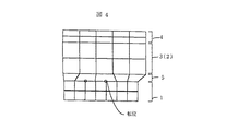
図5に図2の素子の配線部分の平面図を示し、ソース電極とソース接地部分の配置について説明する。この場合、図2の素子が2個並列になっている。中央にドレインコンタクトプラグ17とドレイン配線31があり、その両側にゲートコンタクトプラグ18とゲート配線が音叉状に配列される。その両外側のソース領域にはソースコンタクトプラグ15と基板コンタクト領域が形成され、これらがソース配線30により接続される。
図6に図5の素子を複数配列した場合の配線を平面図として示す。ドレイン、ソース及びゲートがそれぞれ交互に櫛状に配列することによって多数素子を並列接続する。さらにソース配線30の各素子間の領域には基板コンタクト領域が形成されており接地抵抗が小さくなる構造となっている。
上記構造を有する電界効果型半導体装置の製造工程を図7(a)乃至図7(h)を参照し、以下に説明する。なお、図7(a)のみは図2に対して直交する方向、すなわち図3に示したVI(a)―VI(a)方向より見た断面を示したものである。また、図6(b)以降は図1と同一の方向、すなわち図2に示したII−II方向より見た断面図となる。
まず、図1に示した半導体積層構造の半導体ウエハを準備する。そして、図7(a)に示す如く、素子分離領域16を形成する。この素子分離領域16はフォトプロセス、ドライエッチングプロセス、および化学機械研磨プロセスを用いて、深さ300nmの溝を形成し、絶縁膜を埋め込む浅溝分離法により形成される。
次に、図7(b)に示す如く、フォトレジスト20をマスクとし、B(ボロン)イオンを50keVのエネルギーで5×10¹²/cm2程度注入してP型ウェル領域6を形成する。イオン注入後のアニールは瞬時加熱処理(RTA: Rapid Thermal Annealing)により、950℃30秒行う。
次に、図7(c)に示す如く、Si層4に酸窒化処理を行うことにより厚さ8nmのゲート絶縁膜7を形成し、CVDによりP(リン)イオンを5×10²⁰/cm3程度ドープした多結晶Si膜100nmのゲート電極膜8を形成する。ゲート電極はKrFエキシマレーザステッパーによるリソグラフィーとドライエッチングによりゲート長0.18μmに加工する。ゲート加工後、ゲート周辺をさらに5nm程度ライト酸化を行いゲートバーズビークを形成する。
さらに図7(d)に示す如く、フォトレジスト20およびゲート電極8をマスクとして、P(リン)イオンを40keVのエネルギーで2×10¹³/cm2程度注入してN型ドレインオフセット領域10を形成し、図7(e)に示す如くB(ボロン)イオンを25keVのエネルギーで5×1014/cm2程度注入し、P型ウェル領域6内に位置したポケットパンチスルーストッパー11を形成し、さらに図7(f)に示す如くAs(砒素)イオンを50keVのエネルギーで6×1015/cm2程度注入してN型ソース領域9とN型ドレイン領域12を形成する。
この後、図7(g)に示す如く前記半導体積層構造の一部を第2SiGe層3を貫通して第1SiGe層2に達するまで、フォトリソグラフィーとドライエッチングにより開口し、Wsi(タングステンシリサイド)とWの2層構造からなる基板コンタクト領域13の下部を埋め込む。同時にゲート電極膜8の上部もシリサイド化させる。
次に、図7(h)に示す如く、O3-TEOSにより層間絶縁膜19を形成し、一部をフォトリソグラフィーとドライエッチングにより開口してソース・ドレイン・ゲートの各コンタクトプラグ15、17、18(ただし、18は図示されない)と、基板コンタクト領域13の残り上部をWで埋め込む。さらにAlとTiNの積層膜で第1配線層14が形成される。図示していないが、第1配線層14上には、層間絶縁膜19と同様の層間絶縁膜を介して第2配線層が形成される。一方、基板1の底面にはソース電極100が形成される。このソース電極100はニッケル(Ni)、チタン(Ti)、ニッケル(Ni)および半田付け性の良い銀(Ag)層を順次積層することにより形成される。
本トランジスタにおいては、Si層(歪Si)4の電子移動度が通常のSi電界効果トランジスタのそれに比べて70%上昇した効果によって、相互コンダクタンスが従来に比べて50%、電力増幅回路の付加効率が40%向上した。
(実施例2)
本実施例では、SiGe層上に形成されたSi層にチャネルが形成されたPチャネル電界効果型半導体装置を例示する。製造工程は、実施例1の場合と酷似しているため、相違点のみを示す。
図3に示した半導体積層構造は、本実施例ではN型低抵抗Si基板1、N型低抵抗第1SiGe層2、N型高抵抗第2SiGe層3、N型高抵抗Si層4の構成となる。ドーピングガスには前記B2H6の代わりにPH3を用い、不純物濃度は実施例1と同様である。
ウェル領域6およびパンチスルーストッパー11はN型となりBの代わりにPが注入される。ソース領域9、ドレイン領域12、ドレインオフセット領域10はいずれもP型となり、BないしはBF2が注入される。イオン注入の深さと注入量はいずれも実施例1と同様である。また、ゲート電極の多結晶Si膜はBをドープしたP型とする。
本トランジスタにおいては、Si層4の正孔移動度が通常のSi電界効果トランジスタのそれに比べて85%上昇した効果によって、相互コンダクタンスが従来に比べて70%、電力増幅回路の付加効率が60%向上した。
(実施例3)
本実施例では、第2SiGe層3内のSi層4との界面付近にチャネルが形成されたPチャネル電界効果型半導体装置を例示する。製造工程は、実施例2の場合と酷似しているため、相違点のみを示す。
前記半導体積層構造においてSi層4の厚みを15nmとすれば、完成した電界効果型トランジスタのチャネル領域におけるSi層4の厚みは5nm未満になるためチャネルはSi層4内には形成されずに、第2SiGe層3内のSi層4との界面付近にチャネルが形成されるようになる。
本トランジスタにおいては、第2SiGe層3の正孔移動度が通常のSi電界効果トランジスタのそれに比べて2.1倍に上昇した効果によって、相互コンダクタンスが従来に比べて90%、電力増幅回路の付加効率が75%向上した。
(実施例4)
図8に本実施例の電力増幅器終段の回路図を示す。図8はN型トランジスタ21のみを用いたシングルエンドの出力回路を構成している。このN型トランジスタ21は実施例1で説明した構造より成る。
ソースは接地され、ドレインは負荷となるストリップ線路26を介して正電源22に接続されている。ゲートにはバイアス電源23よりバイアス電圧が印加されている。信号は入力部24より加えられ、コンデンサ27とストリップ線路26を経由してゲートに至る。ドレイン側の出力は、ストリップ線路26とコンデンサ27からなる出力整合回路を経由して出力部25より出力される。
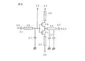
(実施例5)
図9に本実施例の回路図を示す。実施例1と同様のN型トランジスタ21と、実施例2と同様の方法で製造したP型トランジスタ28の各々のドレインを接続し、P型トランジスタのソースは負荷となるストリップ線路26を介して正電源22に接続され、N型トランジスタのソースは負荷となるストリップ線路26を介して負電源29に接続され、コンプリメンタリ回路を形成する。両トランジスタのドレイン電位とバイアス電源23の電位は接地電位に等しくなる。入力側と出力側の回路は図8と同様である。
本実施例によれば、実施例4の場合に比べ、負電源が必要ではあるが、各々40%の電源電圧で同一の出力を得ることが出来、増幅素子の直線性が優れるために出力波形の歪がN型トランジスタ単独の場合に比べて半減した。
また、耐圧に余裕が出来るため、N型トランジスタ単独の場合と同一の電源電圧として出力を7倍に向上させることができた。
また、単一電源で動作させる場合には、負電源29の部分を接地し、バイアス電源23の電位を両トランジスタのドレイン電位、すなわち正電源22の電位の半分にすればよい。ただし、直線性を向上させる目的でP形N形トランジスタの動作点を非対称的に設定する場合にはこの限りではない。単一電源で上記の構成を取った場合でも、正負電源と同様の性能が得られた。
本実施例ではドレイン同士を接続したが、ソース同士を接続しても同様であることは言うまでもない。
(実施例6)
図9に前記実施例1のトランジスタを用いたパワーモジュールの平面図である。
【0006】
図9に示したモジュールはGSM(Global System for
Mobile Communications)とDCS(Digital Cellular System)のデュアルバンド対応としたものである。
【0007】
多層配線形成されたモジュール基板200には、DCSドライバー段(2段)としてDCS用初段トランジスタDCS-TinおよびDCS用中段トランジスタDCS-Tm、DCS出力段としてDCS用出力段トランジスタDCS-Toutが半田付け実装されている。そして、それぞれのトランジスタはワイヤにより所定の配線に電気的接続されている。また、GSMドライバー段(2段)としてGSM用初段トランジスタGSM-TinおよびGSM用中段トランジスタGSM-Tm、GSM出力段としてGSM用出力段トランジスタGSM-Toutが半田付け実装されている。そして、それぞれのトランジスタはワイヤにより所定の配線に電気的接続されている。モジュール基板200の上部にはDCS用入力端子Pin(DCS)、コントローラ端子Vctl、電源端子Vddおよび出力端子Pout(DCS)が配置されている。一方、モジュール基板200の下部にはGSM用入力端子Pin(GSM)、弱い電波を感知し、感度を上げるコントローラ端子Vapc、電源端子Vddおよび出力端子Pout(GSM)が配置されている。抵抗Rはチップ抵抗が、また容量Cはチップコンデンサがインピーダンスマッチング等の理由から半田付け実装されている。なお、回路構成の詳細については省略する。GSM(900MHz)出力としては4W以上、DCS(1800MHz)出力としては2W以上が期待できる。
【0008】
従来、出力段トランジスタの高出力を実現するために、DD-CIMA(Divided Device and Collectively Impedance
Matched Amplifier)が採用された。DD-CIMAの構成は、例えば、 特開平2001-94094号公報に開示されているように、トランジスタチップを2個並列に接続している。
【0009】
一方、本実施例によれば、実施例1で述べたようなチャネル領域に歪Si層が採用され、移動度の向上が図られている。このため、DC-CIMAの構成をとる必要がなくなり、モジュール基板面積が20〜30%減り、小型化が可能になった。
本発明に係わる実施の形態を上述したが、それらの特徴をまとめると以下のとおりである。
(1)本発明の電界効果トランジスタ(MOSFET)の構成は、第1導電型のSi基板一主面上に第1導電型で比較的高不純物濃度の第1SiGe層と、第1導電型で比較的低不純物濃度の第2SiGe層と、第1導電型で比較的低不純物濃度のSi層とが順次積層された半導体積層構造を具備し、前記半導体積層構造の主面上にゲート絶縁膜を介してゲート電極を有し、前記ゲート電極下のチャネル形成領域となる前記第2SiGe層を挟むように、前記第2SiGe層内に第2導電型のソース領域及びドレイン領域が形成され、前記ソース領域に電気的に接続されたリーチスルー層が前記第1SiGe層に到達するように前記第2SiGe層を貫通して形成されていることを特徴とする。 (2)前述した高密度結晶欠陥領域は、Si基板ないしは第1SiGe層の内部にのみ形成されており、前記第1SiGe層と前記第2SiGe層の界面と、前記欠陥領域とは互いに接しない。
(3)第1SiGe層は0.5μm以上3.0μm以下の厚みにする。このことにより、Si基板上に第1SiGe層を形成することにより生じる転位の発生に伴う欠陥領域(0.5μm未満)が、前述したように第1SiGe層およびSi基板内部のみに含まれることになる。
(4)第2SiGe層は0.5μm以上2.5μm以下の厚みにすること、第1SiGe層の不純物濃度は1×1019cm3以上のピーク値とすること、およびしきい値電圧調整のために主面上部より不純物を注入する工程以前の状態での第2SiGe層の不純物濃度を1×1017cm3以下にする。このことにより、前述の如くソース電極と電気的接触をなしているためにソース電極と等電位になっている第1SiGe層と、ドレイン電極の間の電界の分布が均一になる。このため、ドレインリークが低減できる。
(5)前記半導体積層構造主面内のドレイン領域とゲート電極下のチャネル形成領域との中間領域に、第2導電型のドレインオフセット領域を設ける。このことにより、チャネルと平行な方向に対してドレイン電極とソース電極とで形作られる電界を適正な値とすることが出来る。
上述した手段に因れば、ソースおよびドレインによって形成される空乏層領域が、第2SiGe層やドレインオフセット領域内務のみに生じることになり、これらの部分における電界が適正な値となり、高密度の欠陥を含む第1SiGe層およびSi基板は十分に多い不純物濃度と、ソース電極と電気的接触がなされていることのために、等電位となる。このためドレインリーク電流や寄生容量などの性能悪化要因はなくなり、歪SiないしはSiGeによる移動度上昇の効果が最大限に発揮される。
【0010】
(6)前述した素子の構成において、第1導電型をP型、第2導電型をN型とし、第2SiGe層上に形成されるSi層の厚みを5nm以上70nm以下とすれば、前記Si内にチャネルが形成されるNチャネル電界効果型トランジスタとなる。また、第1導電型をN型、第2導電型をP型とし、第2SiGe層上に形成されるSi層の厚みを2nm以下5nm未満とすれば、前記第2SiGe内にチャネルが形成され、前記Si層の厚みを5nm以上70nm以下とすれば、前記Si内にチャネルが形成される、いずれもPチャネル電界効果型トランジスタとなる。
(7)前述したNチャネル電界効果型トランジスタとPチャネル電界効果型トランジスタを各々のソース電極ないしはドレイン電極において直列に接続すれば、コンプリメンタリ増幅回路を構成することが出来、各々のトランジスタのしきい値付近におけるドレイン電流の非線形性がキャンセルされるために、増幅回路の歪特性が向上する。
(8)前述の如くチャネルコンダクタンスを上昇せしめるために、Si層に十分な歪を与え、或いはSiGe層の移動度を上昇せしめるためには、第2SiGe層のGe含有率は5%以上あることが必要であり、望ましくは30%程度必要であるが、50%を超えると移動度上昇の効果が飽和し、結晶品質の悪化のために耐圧が低下するという弊害が生ずるため、上記5%以上50%以下の範囲が望ましい。
【0011】
(9)第2SiGe層の主面と平行面内の格子定数(aとする)と、バルク単結晶Siの格子定数(bとする)との差は、第2SiGe層と同一のGe含有率を有するバルク単結晶SiGeの格子定数(cとする)とバルク単結晶Siの格子定数との差の、70%以上100%以下であることが、上記Si層に十分な歪を与えるために必要になる。これを式で示せば、
0.7≦(a-b)/(c-b)≦1.0
となる。
(10)上記の如く、第2SiGe層の格子定数をバルク単結晶SiGeのそれに近づけるためには、前記(4)に記載したように第1SiGeに十分な厚みを持たせれば良いが、さらに、第1SiGe層のGe含有率をSi基板の上方、膜厚方向に沿って増大させて行くことが、より望ましい。このことは同時に、前記したように第1SiGe層内に存在する高密度欠陥層を第1SiGe層とSi基板界面付近に位置せしめ、第2SiGe層と離間せしめるためにも有効である。
(11)第1第2SiGe層とその上のSi層との積層構造に大きな熱負荷を与えると、Geが拡散すると同時に前記Si層の歪が緩和されてしまうため、好ましくない。従って、電界効果トランジスタの素子間分離領域には、従来よりよく行われている局所的熱酸化法ではなく、浅溝素子分離法、すなわち前記積層構造のSi層と第2SiGe層に溝を形成し、全面に絶縁物を堆積させ、研磨により平坦化させる方法、がより適している。
【0012】
(12)ソース電極と前記高不純物濃度の第1SiGe層ないしは基板とは、電気的接触がなされる必要がある。従来のSi電界効果型トランジスタの場合には、高不純物濃度のSi基板上に成長した低不純物濃度のエピタキシャルSi層の前記接触領域に高濃度のイオン注入を行い、高温かつ長時間の熱処理により、Si基板との電気的接触を行っていた。本発明の電界効果型半導体装置の場合には前述のように、許容熱負荷に限界があるためこの方法は望ましくない。そこで、前記接触領域において、低不純物濃度の第2SiGe層、あるいは第2SiGe層に加えて第1SiGe層の一部または全部を除去し、しかる後にこの部分に導電性物質を堆積することにより、ソース電極と基板部分との電気的接続を行う。通常のSiを用いた電界効果トランジスタでは、例えば、特開平4-196440号公報に開示されているように、低抵抗Si基板に達するまで高抵抗Siを除去してタングステンあるいは多結晶Siを埋め込む方法が開示されているが、埋め込む材料による優劣は考慮されていない。これに対して、本発明のトランジスタではSiチャネル層の歪制御が性能に大きな影響を与えるという大きな特徴を有する。このため、埋め込みに用いる材料の選定も重要になる。多結晶Siを埋め込んだ場合にはチャネル層に対して圧縮歪を与えるが、CVDにより堆積したタングステンや、コバルトシリサイド等、あるいは窒化タングステン等をバリアメタル層としてめっきで形成した銅を堆積した場合には多結晶Siとは異なり金属の塑性のためにチャネル層に対して歪を与える悪影響がないことを見出した。したがって、ソース電極接地(リーチスルー)用の材料としては金属ないしは金属シリサイドを用いることが望ましい。図11にその実施態様を示す。金属ないしは金属シリサイド13は第2SiGe層内に埋め込み形成されている。このようにするとソース電極の直列抵抗が低減できると同時に、素子の動作に伴いチャネル付近で発生する熱を熱伝導率の悪い高抵抗第2SiGe層を介さずとも電極配線を通じて基板側へバイパスすることにより放熱効果が高まるという利点も生ずる。
(13)本発明の、ソース接地型高周波電力増幅用電界効果型半導体装置電界効果トランジスタでは、複数の素子を並列に接続した構造をとる。この場合に、ドレイン電極を列状に複数配置し、その両外側にゲート電極を列状に複数配置し、さらにその両外側にソース電極を列状に配置し、この組を単位としてさらにそれを複数並列する。ソース電極列の外側に前記第1SiGe層ないしは基板の露出領域を設けることによってソース接地抵抗を低減することが可能になる。さらに上記露出領域がソース領域に平行した溝状の構造をとるようにすると、チャネル領域でソース近傍からドレイン近傍に向かってSi層の歪が増大するような歪分布をとることになる。歪が増大すると歪Siの伝導帯のエネルギーが低下する。つまり、ソースからドレイン方向に歪が増大する構造をとることによって、同じドレイン電圧を印加してもチャネルの横方向電界はより強くなり、ドレイン電流が増大する。このため、溝の位置をソース外側とすることはトランジスタの性能を高めるためにも必要な方法となる。前記したソース電極接地用材料の選択もこの目的に適っている。
(14)ゲート電極には、製造工程(加工プロセス)の容易さ、またしきい値電圧の制御性の点で多結晶Siを用いることが望ましい。ゲート電極の抵抗を下げるために多結晶Siの上部に金属シリサイド層を設けることも有効である。しかしながら、ゲート電極の材料に関しては、これのみに限定されるものではなく、例えば多結晶Siの代わりに多結晶SiGeを用いることや、多結晶Si等でダミーのゲート電極を形成し、しかる後にこれを除去し、金属を埋め込む方法を用いることも可能である。
【0013】
【発明の効果】
本発明によれば移動体端末に使用される電力増幅用電界効果型トランジスタの付加効率を大幅に向上させることが可能になる。
【図面の簡単な説明】
【図1】本発明の実施例1に係わるNチャネル電界効果型半導体装置の主要部分の断面図である。
【図2】本発明の実施例1に係わるNチャネル電界効果型半導体装置の主要部分の平面図である。
【図3】本発明の実施例1に係わる半導体積層構造の断面図である。
【図4】本発明の実施例1に係わる半導体積層構造の格子配列のモデル図である
【図5】本発明の実施例1に係わるNチャネル電界効果型半導体装置の主要部分の平面図である。
【図6】本発明の実施例1に係わるNチャネル電界効果型半導体装置の主要部分の平面図である。
【図7】本発明の実施例1に係わるNチャネル電界効果型半導体装置の製造工程の断面図である。
【図8】本発明の実施例4に係わる電力増幅器手段の回路図である。
【図9】本発明の実施例5に係わる電力増幅器手段の回路図である。
【図10】本発明の実施例5に係わるパワーモジュールの平面図である。
【図11】本発明の他の実施形態を示す断面図である。
【符号の説明】
1…P型低抵抗Si基板、2…P型低抵抗第1SiGe層、3…P型高抵抗第2SiGe層、4…P型高抵抗Si層、5…高欠陥密度領域、6…P型ウェル、7…ゲート絶縁膜、8…ゲート電極、9…N型ソース領域、10…N型ドレインオフセット領域、11…ポケットパンチスルーストッパー、12…N型ドレイン領域、13…基板コンタクト領域、14…第1配線層、15…ソースコンタクトプラグ、16…素子分離領域、17…ドレインコンタクトプラグ、18…ゲートコンタクトプラグ、19…層間絶縁膜、20…フォトレジスト、21…N型トランジスタ、22…正電源、23…バイアス電源、24…入力部、25…出力部、26…ストリップ線路、27…コンデンサ、28…P形トランジスタ、29…負電源、30…ソース配線、31…ドレイン配線、32…ゲート配線。[0001]
BACKGROUND OF THE INVENTION
The present invention relates to a field effect semiconductor device, and more particularly to a technique effective when applied to a field effect semiconductor device for high frequency power amplification of 800 MHz or more used for a mobile communication device.
[0002]
[Prior art]
With the rapid spread of mobile communication terminals in recent years, there has been an increasing demand for power amplifiers for portable terminals with lower power consumption and higher efficiency. As the power amplification element for this application, a transistor (HBT) using a compound semiconductor, an insulated gate field effect transistor (Si-MOSFET) using a silicon semiconductor (Si), and the like are used.
A power amplifier using a compound semiconductor is described in, for example, IEEE Journal of Solid-State Circuits, Volume: 35 Issue: 8, p.1109-1120 (2000) (Reference 1).
On the other hand, power amplifiers using Si-MOSFETs are described in detail in, for example, IEDM99 Technical Digest (1999), pp. 205-208 (Reference 2) or Japanese Patent Laid-Open No. 2001-94094 (Reference 3).
By the way, the phenomenon that the mobility is increased by using strained Si or SiGe mixed crystal is shown in, for example, J. Appl. Phys. 80 (1996), p. 2234 (Reference 4).
A method for improving the performance of a transistor (MOSFET) in an IC (specifically, a CMOSIC) using this phenomenon is disclosed in, for example, Japanese Patent Laid-Open No. 10-270685 (Reference 5) and Japanese Patent Laid-Open No. 11-340337 ( Document 6).
The technique described in
In addition, the technique described in
[0003]
[Problems to be solved by the invention]
When the above compound semiconductor is applied, the high unit cost of the wafer has been a problem.
On the other hand, when a silicon semiconductor (Si) as disclosed in
However, there was a limit to high efficiency due to the physical properties of Si. Specifically, reducing the gate oxide thickness and shortening the channel length has been effective in improving Si-MOSFET performance, but such scaling is no longer directly improving performance. I came. That is, the effective mobility of the channel decreases as the scaling progresses. This is because a strong electric field is applied to the interface of the gate oxide film, the carrier density is high, and carrier scattering increases. For this reason, carriers are pressed against the interface of the gate oxide film, and the carrier mobility is lowered. Therefore, there was a limit to the reduction of channel conductance that affects the performance of Si-MOSFET.
In order to improve the effective mobility, it may be possible to control the impurity profile that relaxes the electric field in the channel. However, this is also the limit of the threshold voltage, especially the power supply voltage (high frequency power amplification MOSFET) However, since there is a limit to the decrease in the lithium battery (3.5V), it has become impossible to play a significant role in improving the performance.
As other means for improving the effective mobility, the inventors disclosed the techniques disclosed in the above-mentioned
The techniques disclosed in
However, in the high-frequency power amplification MOSFET described in
That is, in the high-frequency power amplification MOSFET described in
An object of the present invention is to provide a technique for improving mutual conductance while ensuring a drain withstand voltage in a semiconductor device for high frequency power amplification.
Another object of the present invention is to provide a technique for reducing the size and weight of a high-frequency power amplifier.
The above and other objects and novel features of the present invention will be apparent from the description of this specification and the accompanying drawings.
[Means for Solving the Problems]
Of the inventions disclosed in this application, the outline of typical ones will be briefly described as follows.
A typical power amplification field effect semiconductor device according to the present invention includes a first conductivity type first SiGe layer of a relatively high impurity concentration on a main surface of a first conductivity type Si substrate, and a first conductivity type. A semiconductor laminated structure in which a second SiGe layer having a relatively low impurity concentration and a Si layer having a first conductivity type and a relatively low impurity concentration are sequentially laminated, and a gate insulating film is formed on a main surface of the semiconductor laminated structure. A source region and a drain region of the second conductivity type are formed in the second SiGe layer so as to sandwich a Si layer that becomes a channel formation region under the gate electrode, An electrically connected reach-through layer is formed to penetrate the second SiGe layer so as to reach the first SiGe layer.
According to the above-described means, a region containing a large amount of crystal defects (dislocations) caused by bonds having different lattice sizes is confined by the first SiGe layer having a relatively high impurity concentration. The depletion layer extending from the drain region sufficiently extends into the first SiGe layer having a relatively low impurity concentration, and the extension is suppressed when reaching the first SiGe layer having a high impurity concentration. For this reason, the depletion layer does not extend to a region containing a large amount of crystal defects (dislocations). Therefore, the drain breakdown voltage can be secured by extending the depletion layer in the second SiGe layer (low concentration layer), and the leakage current can be reduced by suppressing the extension of the depletion layer in the first SiGe layer (high concentration layer). Further, strain Si having tensile strain is formed on the surface of the second SiGe layer, and since this strain Si is used as a channel region, the band structure changes due to strain, and the carrier mobility is higher than that of unstrained Si. About 70% improvement. Therefore, the mutual conductance can be improved, and a high-performance power amplification semiconductor device can be obtained.
[0004]
DETAILED DESCRIPTION OF THE INVENTION
Hereinafter, embodiments of the present invention will be described in detail with reference to the drawings.
[0005]
Example 1
In this embodiment, an N-channel field effect semiconductor device in which a channel is formed in a Si layer formed on a SiGe layer is illustrated.
FIG. 1 is a main cross-sectional view of an N-channel field effect semiconductor device according to the first embodiment, and FIG. 2 is a plan view of the N-channel field effect semiconductor device. The cross-sectional view of FIG. 1 shows a section taken along II in FIG. Prior to the description of FIGS. 1 and 2, a semiconductor stacked structure used for manufacturing the field effect semiconductor device of the first embodiment will be described with reference to FIGS. 3 and 4.
As shown in FIG. 3, the semiconductor laminated structure used for manufacturing the field effect semiconductor device of the first embodiment has a P-type low-resistance
Next, residual B inside the vapor phase growth apparatus 2 H 6 After performing a cleaning process to reduce the gas partial pressure, the
Followed by GeH Four The gas is stopped and a P-type high
The cross section of the semiconductor multilayer structure manufactured through the above steps was observed with a transmission electron microscope. In FIG. 3, as indicated by the oblique lines, dislocation loops were observed over a region of 500 nm above and below centering on the interface between the
As shown in FIG. 4, in the laminated structure of the
Next, the structure of the field effect semiconductor device having the semiconductor laminated structure manufactured in the above process will be described.
As shown in FIG. 1, a P-
Further, an N-
A
As shown in FIG. 2, the width of the channel region of the element (that is, the channel width) is defined by the interval between the
FIG. 5 is a plan view of the wiring portion of the element of FIG. 2, and the arrangement of the source electrode and the source grounded portion will be described. In this case, two elements of FIG. 2 are arranged in parallel. The
FIG. 6 is a plan view showing wiring when a plurality of elements shown in FIG. 5 are arranged. Multiple elements are connected in parallel by alternately arranging drains, sources and gates in a comb shape. Further, a substrate contact region is formed in a region between the elements of the
A manufacturing process of the field effect semiconductor device having the above structure will be described below with reference to FIGS. 7 (a) to 7 (h). FIG. 7 (a) only shows a cross section viewed from the direction orthogonal to FIG. 2, that is, the VI (a) -VI (a) direction shown in FIG. Further, FIG. 6B and subsequent figures are cross-sectional views seen from the same direction as FIG. 1, that is, the II-II direction shown in FIG.
First, a semiconductor wafer having the semiconductor laminated structure shown in FIG. 1 is prepared. Then, as shown in FIG. 7A, an
Next, as shown in FIG. 7B, the
Next, as shown in FIG. 7C, an oxynitridation process is performed on the
Further, as shown in FIG. 7 (d), using the
Thereafter, as shown in FIG. 7 (g), a part of the semiconductor stacked structure is opened by photolithography and dry etching until it reaches the
Next, as shown in FIG. Three An interlayer insulating
In this transistor, the electron mobility of the Si layer (strained Si) 4 is increased by 70% compared to that of a normal Si field effect transistor, so that the mutual conductance is 50% compared to the conventional case, and the added efficiency of the power amplifier circuit Improved by 40%.
(Example 2)
In this embodiment, a P-channel field effect semiconductor device in which a channel is formed in a Si layer formed on a SiGe layer is illustrated. Since the manufacturing process is very similar to that of the first embodiment, only the differences are shown.
The semiconductor laminated structure shown in FIG. 3 has the structure of an N-type low-
The
In this transistor, the hole mobility of the
(Example 3)
In this embodiment, a P-channel field effect semiconductor device in which a channel is formed near the interface with the
If the thickness of the
In this transistor, the hole mobility of the
Example 4
FIG. 8 shows a circuit diagram of the final stage of the power amplifier of this embodiment. FIG. 8 shows a single-ended output circuit using only the N-
The source is grounded, and the drain is connected to the
(Example 5)
FIG. 9 shows a circuit diagram of this embodiment. The drain of each of the N-
According to the present embodiment, a negative power supply is required as compared with the case of the fourth embodiment. However, the same output can be obtained at a power supply voltage of 40%, and the output waveform is excellent because the linearity of the amplifying element is excellent. Was halved compared to the case of the N-type transistor alone.
In addition, since the withstand voltage can be afforded, the output can be improved seven times as the same power supply voltage as that of the N-type transistor alone.
In the case of operating with a single power source, the
In this embodiment, the drains are connected to each other, but it goes without saying that the same is true even if the sources are connected to each other.
(Example 6)
FIG. 9 is a plan view of a power module using the transistor of the first embodiment.
[0006]
The module shown in FIG. 9 is GSM (Global System for
Mobile Communications) and DCS (Digital Cellular System) dual band compatible.
[0007]
The
[0008]
Conventionally, to achieve high output of output stage transistors, DD-CIMA (Divided Device and Collectively Impedance
Matched Amplifier) was adopted. The DD-CIMA has a configuration in which two transistor chips are connected in parallel as disclosed in, for example, Japanese Patent Laid-Open No. 2001-94094.
[0009]
On the other hand, according to the present embodiment, a strained Si layer is employed in the channel region as described in the first embodiment, and the mobility is improved. For this reason, it is not necessary to adopt the DC-CIMA configuration, the module substrate area is reduced by 20 to 30%, and miniaturization is possible.
Although the embodiment according to the present invention has been described above, the features are summarized as follows.
(1) The structure of the field effect transistor (MOSFET) of the present invention is compared with the first conductivity type and the first conductivity type first SiGe layer on the main surface of the first conductivity type Si substrate and the first conductivity type. A semiconductor stacked structure in which a second SiGe layer having a low impurity concentration and a Si layer having a first conductivity type and a relatively low impurity concentration are sequentially stacked, and a gate insulating film is interposed on the main surface of the semiconductor stacked structure. A second conductivity type source region and drain region are formed in the second SiGe layer so as to sandwich the second SiGe layer serving as a channel formation region under the gate electrode. An electrically connected reach-through layer is formed to penetrate the second SiGe layer so as to reach the first SiGe layer. (2) The above-described high-density crystal defect region is formed only within the Si substrate or the first SiGe layer, and the interface between the first SiGe layer and the second SiGe layer and the defect region do not contact each other.
(3) The first SiGe layer is 0.5 μm or more and 3.0 μm or less in thickness. As a result, a defect region (less than 0.5 μm) associated with the occurrence of dislocations generated by forming the first SiGe layer on the Si substrate is included only in the first SiGe layer and the Si substrate as described above.
(4) The thickness of the second SiGe layer is 0.5 μm or more and 2.5 μm or less, and the impurity concentration of the first SiGe layer is 1 × 10 19 cm Three The impurity concentration of the second SiGe layer before the step of implanting impurities from the upper part of the main surface for adjusting the threshold voltage and the threshold voltage is 1 × 10 17 cm Three Below. As a result, the electric field distribution between the drain electrode and the first SiGe layer that is at the same potential as the source electrode due to the electrical contact with the source electrode as described above becomes uniform. For this reason, drain leakage can be reduced.
(5) In the main surface of the semiconductor multilayer structure Drain region When Channel formation region under the gate electrode A drain offset region of the second conductivity type is provided in the intermediate region. Thereby, the electric field formed by the drain electrode and the source electrode in the direction parallel to the channel can be set to an appropriate value.
According to the above-described means, the depletion layer region formed by the source and the drain is generated only in the second SiGe layer and the drain offset region, and the electric field in these portions becomes an appropriate value, and the high density defect The first SiGe layer containing Si and the Si substrate are equipotential because of a sufficiently high impurity concentration and electrical contact with the source electrode. As a result, performance deterioration factors such as drain leakage current and parasitic capacitance are eliminated, and the effect of increasing the mobility due to strained Si or SiGe is maximized.
[0010]
(6) In the configuration of the element described above, if the first conductivity type is P type, the second conductivity type is N type, and the thickness of the Si layer formed on the second SiGe layer is 5 nm or more and 70 nm or less, the Si An N-channel field effect transistor having a channel formed therein is obtained. If the first conductivity type is N-type, the second conductivity type is P-type, and the thickness of the Si layer formed on the second SiGe layer is 2 nm or less and less than 5 nm, a channel is formed in the second SiGe, If the thickness of the Si layer is 5 nm or more and 70 nm or less, a channel is formed in the Si, and both are P-channel field effect transistors.
(7) If the N-channel field-effect transistor and the P-channel field-effect transistor described above are connected in series at each source electrode or drain electrode, a complementary amplifier circuit can be constructed, and the threshold value of each transistor Since the non-linearity of the drain current in the vicinity is canceled, the distortion characteristics of the amplifier circuit are improved.
(8) As described above, in order to increase the channel conductance, in order to give sufficient strain to the Si layer or increase the mobility of the SiGe layer, the Ge content of the second SiGe layer may be 5% or more. Necessary, desirably about 30% is necessary, but if it exceeds 50%, the effect of increasing the mobility is saturated, and the adverse effect that the pressure resistance decreases due to the deterioration of crystal quality. A range below% is desirable.
[0011]
(9) The difference between the lattice constant (referred to as “a”) in the principal plane and parallel plane of the second SiGe layer and the lattice constant (referred to as “b”) of bulk single crystal Si is the same Ge content as the second SiGe layer. 70% or more and 100% or less of the difference between the lattice constant of bulk single crystal SiGe (with c) and the bulk single crystal Si lattice constant is necessary to give sufficient strain to the Si layer Become. If this is expressed by an expression,
0.7 ≦ (ab) / (cb) ≦ 1.0
It becomes.
(10) As described above, in order to bring the lattice constant of the second SiGe layer closer to that of the bulk single crystal SiGe, the first SiGe may have a sufficient thickness as described in the above (4). It is more desirable to increase the Ge content of the 1SiGe layer along the film thickness direction above the Si substrate. This is also effective for positioning the high-density defect layer existing in the first SiGe layer in the vicinity of the interface between the first SiGe layer and the Si substrate as described above and separating from the second SiGe layer.
(11) When a large thermal load is applied to the laminated structure of the first second SiGe layer and the Si layer thereon, Ge is diffused and strain of the Si layer is alleviated at the same time. Therefore, in the element isolation region of the field effect transistor, a groove is formed in the shallow trench isolation method, that is, the Si layer and the second SiGe layer in the stacked structure, instead of the local thermal oxidation method that is conventionally performed. A method of depositing an insulator on the entire surface and flattening by polishing is more suitable.
[0012]
(12) The source electrode and the first SiGe layer or substrate having a high impurity concentration need to be in electrical contact. In the case of a conventional Si field effect transistor, high concentration ion implantation is performed on the contact region of a low impurity concentration epitaxial Si layer grown on a high impurity concentration Si substrate, and heat treatment is performed at a high temperature for a long time. It was in electrical contact with the Si substrate. In the case of the field effect semiconductor device of the present invention, this method is not desirable because the allowable heat load is limited as described above. Therefore, in the contact region, the second SiGe layer having a low impurity concentration, or a part or all of the first SiGe layer in addition to the second SiGe layer is removed, and then a conductive material is deposited on this portion to thereby form the source electrode. Is electrically connected to the substrate portion. In a field effect transistor using ordinary Si, for example, as disclosed in Japanese Patent Application Laid-Open No. 4-196440, a method of removing high resistance Si until it reaches a low resistance Si substrate and embedding tungsten or polycrystalline Si However, superiority or inferiority due to the embedding material is not considered. On the other hand, the transistor of the present invention has a great feature that the strain control of the Si channel layer greatly affects the performance. For this reason, selection of the material used for embedding is also important. When polycrystalline silicon is embedded, compressive strain is applied to the channel layer, but when depositing copper deposited by CVD using tungsten deposited by CVD, cobalt silicide, or tungsten nitride as a barrier metal layer We found that unlike polycrystalline Si, there is no adverse effect on the channel layer due to the plasticity of the metal. Therefore, it is desirable to use metal or metal silicide as a material for grounding the source electrode (reach through). FIG. 11 shows the embodiment. The metal or
(13) The field-effect semiconductor device field-effect transistor for grounded source type high frequency power amplification of the present invention has a structure in which a plurality of elements are connected in parallel. In this case, a plurality of drain electrodes are arranged in a row, a plurality of gate electrodes are arranged in a row on both outer sides thereof, and a source electrode is arranged in a row on both outer sides thereof. Multiple parallels. By providing the first SiGe layer or the exposed region of the substrate outside the source electrode array, the source ground resistance can be reduced. Further, when the exposed region has a groove-like structure parallel to the source region, the channel region has a strain distribution such that the strain of the Si layer increases from the vicinity of the source to the vicinity of the drain. As the strain increases, the energy of the conduction band of strained Si decreases. In other words, by adopting a structure in which the strain increases from the source to the drain, the lateral electric field of the channel becomes stronger and the drain current increases even when the same drain voltage is applied. For this reason, setting the groove to the outside of the source is a necessary method for improving the performance of the transistor. The selection of the source electrode grounding material is also suitable for this purpose.
(14) For the gate electrode, it is desirable to use polycrystalline Si in terms of ease of manufacturing process (processing process) and controllability of threshold voltage. In order to reduce the resistance of the gate electrode, it is also effective to provide a metal silicide layer on top of the polycrystalline Si. However, the material of the gate electrode is not limited to this. For example, polycrystalline SiGe is used instead of polycrystalline Si, or a dummy gate electrode is formed of polycrystalline Si or the like, and then this is performed. It is also possible to use a method of removing metal and embedding metal.
[0013]
【The invention's effect】
ADVANTAGE OF THE INVENTION According to this invention, it becomes possible to improve significantly the additional efficiency of the field effect type transistor for power amplification used for a mobile terminal.
[Brief description of the drawings]
FIG. 1 is a cross-sectional view of a main portion of an N-channel field effect semiconductor device according to
FIG. 2 is a plan view of a main part of an N-channel field effect semiconductor device according to Example 1 of the invention.
FIG. 3 is a cross-sectional view of a semiconductor multilayer structure according to Example 1 of the present invention.
FIG. 4 is a model diagram of a lattice arrangement of a semiconductor multilayer structure according to Example 1 of the present invention.
FIG. 5 is a plan view of the main part of the N-channel field effect semiconductor device according to the first embodiment of the invention.
FIG. 6 is a plan view of the main part of the N-channel field effect semiconductor device according to the first embodiment of the invention.
FIG. 7 is a cross-sectional view of the manufacturing process of the N-channel field effect semiconductor device according to the first embodiment of the invention.
FIG. 8 is a circuit diagram of power amplifier means according to
FIG. 9 is a circuit diagram of power amplifier means according to a fifth embodiment of the present invention.
FIG. 10 is a plan view of a power module according to
FIG. 11 is a cross-sectional view showing another embodiment of the present invention.
[Explanation of symbols]
DESCRIPTION OF
Claims (18)
前記半導体積層構造の主面上にゲート絶縁膜を介してゲート電極を有し、
前記ゲート電極下のチャネル形成領域となる前記Si層を挟むように、前記Si層内および前記第2SiGe層内に前記第1導電型とは逆の第2導電型のソース領域及びドレイン領域が形成され、
前記ドレイン領域と前記ゲート電極下のチャネル形成領域との中間領域に、前記第2導電型のドレインオフセット領域が前記ゲート電極に対して自己整合的に形成され、
前記ソース領域に電気的に接続された基板コンタクト領域が前記第1SiGe層に到達するように前記第2SiGe層を貫通して形成されている
ことを特徴とする電力増幅用電界効果型半導体装置。A first conductivity type first SiGe layer, a first conductivity type second SiGe layer having a lower impurity concentration than the first SiGe layer, and a first conductivity type on a main surface of a first conductivity type Si substrate. A semiconductor stacked structure in which a Si layer having a lower impurity concentration than the first SiGe layer is sequentially stacked;
Having a gate electrode on the main surface of the semiconductor multilayer structure through a gate insulating film;
A source region and a drain region of a second conductivity type opposite to the first conductivity type are formed in the Si layer and the second SiGe layer so as to sandwich the Si layer to be a channel formation region under the gate electrode. And
A drain offset region of the second conductivity type is formed in a self-aligned manner with respect to the gate electrode in an intermediate region between the drain region and a channel formation region under the gate electrode;
A field effect semiconductor device for power amplification, wherein a substrate contact region electrically connected to the source region is formed so as to penetrate the second SiGe layer so as to reach the first SiGe layer.
前記半導体積層構造の主面上にゲート絶縁膜を介してゲート電極を有し、
前記ゲート電極下のチャネル形成領域となる前記第2SiGe層を挟むように、前記第2SiGe層内に前記第1導電型とは逆の第2導電型のソース領域及びドレイン領域が形成され、
前記ドレイン領域と前記ゲート電極下のチャネル形成領域との中間領域に、前記第2導電型のドレインオフセット領域が前記ゲート電極に対して自己整合的に形成され、
前記ソース領域に電気的に接続された基板コンタクト領域が前記第1SiGe層に到達するように前記第2SiGe層を貫通して形成されている
ことを特徴とする電力増幅用電界効果型半導体装置。A first conductivity type first SiGe layer, a first conductivity type second SiGe layer having a lower impurity concentration than the first SiGe layer, and a first conductivity type on a main surface of a first conductivity type Si substrate. A semiconductor stacked structure in which a Si layer having a lower impurity concentration than the first SiGe layer is sequentially stacked;
Having a gate electrode on the main surface of the semiconductor multilayer structure through a gate insulating film;
A source region and a drain region of a second conductivity type opposite to the first conductivity type are formed in the second SiGe layer so as to sandwich the second SiGe layer serving as a channel formation region under the gate electrode,
A drain offset region of the second conductivity type is formed in a self-aligned manner with respect to the gate electrode in an intermediate region between the drain region and a channel formation region under the gate electrode;
A field effect semiconductor device for power amplification, wherein a substrate contact region electrically connected to the source region is formed so as to penetrate the second SiGe layer so as to reach the first SiGe layer.
(2)前記第1SiGe層主面に前記第1導電型で、前記第1SiGe層より低不純物濃度の第2SiGe層を形成する工程と、
(3)前記第2SiGe層主面に前記第1導電型で、前記第1SiGe層より低不純物濃度のSi層を形成する工程と、
(4)前記第1SiGe層、前記第2SiGe層および前記Si層が積層されてなる半導体積層構造主面に活性領域を分離するための溝を形成する工程と、
(5)前記溝に絶縁物を埋める工程と、
(6)前記活性領域内に不純物を注入する工程と、
(7)前記活性領域表面にゲート絶縁膜を形成する工程と、
(8)前記ゲート絶縁膜上にゲート電極を形成する工程と、
(9)前記活性領域内に前記第1導電型とは逆の第2導電型のドレインオフセット領域を前記ゲート電極に対し自己整合形成する工程と、
(10)前記活性領域内に、前記ゲート電極端から離間して、前記ゲート電極に対し自己整合された前記ドレインオフセット領域に接し、かつ、前記ドレインオフセット領域よりも高不純物濃度を有するドレイン領域を、前記ドレイン領域と前記ゲート電極下のチャネル形成領域との中間領域に前記ドレインオフセット領域が位置するように形成すると共に、前記ゲート電極に対し自己整合されたソース領域を形成する工程と、
(11)前記ソース領域近傍の領域で前記第1SiGe層ないしは前記Si基板を露出し、露出部分を形成する工程と、
(12)前記露出部分と前記ソース領域とを金属ないしは金属シリサイドにより接続する工程と
を含むことを特徴とする電力増幅用電界効果型半導体装置の製造方法。(1) forming a first SiGe layer of the first conductivity type on a main surface of the first conductivity type Si substrate;
(2) forming a second SiGe layer of the first conductivity type and having a lower impurity concentration than the first SiGe layer on the first SiGe layer main surface;
(3) forming a Si layer of the first conductivity type on the main surface of the second SiGe layer and having a lower impurity concentration than the first SiGe layer;
(4) forming a groove for separating an active region in a main surface of a semiconductor stacked structure formed by stacking the first SiGe layer, the second SiGe layer, and the Si layer;
(5) filling the trench with an insulator;
(6) implanting impurities into the active region;
(7) forming a gate insulating film on the surface of the active region;
(8) forming a gate electrode on the gate insulating film;
(9) forming a drain offset region of a second conductivity type opposite to the first conductivity type in the active region with respect to the gate electrode;
(10) A drain region that is spaced apart from the gate electrode end, is in contact with the drain offset region that is self-aligned with the gate electrode, and has a higher impurity concentration than the drain offset region. Forming the drain offset region in an intermediate region between the drain region and the channel formation region under the gate electrode, and forming a source region self-aligned with the gate electrode;
(11) exposing the first SiGe layer or the Si substrate in a region near the source region and forming an exposed portion;
(12) A method of manufacturing a field effect semiconductor device for power amplification, comprising a step of connecting the exposed portion and the source region with a metal or metal silicide.
前記電力増幅用電界効果型半導体装置が、
第1導電型のSi基板一主面上に前記第1導電型の第1SiGe層と、前記第1導電型で、前記第1SiGe層より低不純物濃度の第2SiGe層と、前記第1導電型で、前記第1SiGe層より低不純物濃度のSi層とが順次積層された半導体積層構造を具備し、
前記半導体積層構造の主面上にゲート絶縁膜を介してゲート電極を有し、
前記ゲート電極下のチャネル形成領域となる前記Si層を挟むように、前記Si層内および前記第2SiGe層内に前記第1導電型とは逆の第2導電型のソース領域及びドレイン領域が形成され、
前記ドレイン領域と前記ゲート電極下のチャネル形成領域との中間領域に、前記第2導電型のドレインオフセット領域が前記ゲート電極に対して自己整合的に形成され、
前記ソース領域に電気的に接続された基板コンタクト領域が前記第1SiGe層に到達するように前記第2SiGe層を貫通して形成されている
ことを特徴とするパワーモジュール。A power module that uses a field effect semiconductor device for power amplification in each of a driver stage and an output stage,
The field-effect semiconductor device for power amplification,
A first conductivity type first SiGe layer, a first conductivity type second SiGe layer having a lower impurity concentration than the first SiGe layer, and a first conductivity type on a main surface of a first conductivity type Si substrate. A semiconductor stacked structure in which a Si layer having a lower impurity concentration than the first SiGe layer is sequentially stacked;
Having a gate electrode on the main surface of the semiconductor multilayer structure through a gate insulating film;
A source region and a drain region of a second conductivity type opposite to the first conductivity type are formed in the Si layer and the second SiGe layer so as to sandwich the Si layer to be a channel formation region under the gate electrode. And
A drain offset region of the second conductivity type is formed in a self-aligned manner with respect to the gate electrode in an intermediate region between the drain region and a channel formation region under the gate electrode;
A power module, wherein a substrate contact region electrically connected to the source region is formed through the second SiGe layer so as to reach the first SiGe layer.
前記半導体積層構造の主面上にゲート絶縁膜を介してゲート電極を有し、
前記第2SiGe層および前記Si層の主面一部に前記第1導電型のウェル領域を有し、
前記ゲート電極下のチャネル形成領域となる前記Si層を挟むように、前記Si層内および前記第2SiGe層内に前記第1導電型とは逆の第2導電型のソース領域及びドレイン領域が形成され、
前記ドレイン領域と前記ゲート電極下のチャネル形成領域との中間領域に、前記第2導電型のドレインオフセット領域が前記ゲート電極に対して自己整合的に形成され、
前記ソース領域に電気的に接続された基板コンタクト領域が前記第1SiGe層に到達するように前記第2SiGe層を貫通して形成されている
ことを特徴とする電力増幅用電界効果型半導体装置。A first conductivity type first SiGe layer, a first conductivity type second SiGe layer having a lower impurity concentration than the first SiGe layer, and a first conductivity type on a main surface of a first conductivity type Si substrate. A semiconductor stacked structure in which a Si layer having a lower impurity concentration than the first SiGe layer is sequentially stacked;
Having a gate electrode on the main surface of the semiconductor multilayer structure through a gate insulating film;
The first conductivity type well region in a part of a main surface of the second SiGe layer and the Si layer;
A source region and a drain region of a second conductivity type opposite to the first conductivity type are formed in the Si layer and the second SiGe layer so as to sandwich the Si layer to be a channel formation region under the gate electrode. And
A drain offset region of the second conductivity type is formed in a self-aligned manner with respect to the gate electrode in an intermediate region between the drain region and a channel formation region under the gate electrode;
A field effect semiconductor device for power amplification, wherein a substrate contact region electrically connected to the source region is formed so as to penetrate the second SiGe layer so as to reach the first SiGe layer.
Priority Applications (3)
| Application Number | Priority Date | Filing Date | Title |
|---|---|---|---|
| JP2001305929A JP4799786B2 (en) | 2001-10-02 | 2001-10-02 | Field effect semiconductor device for power amplification, method for manufacturing the same, and power module |
| US10/259,396 US6815707B2 (en) | 2001-10-02 | 2002-09-30 | Field-effect type semiconductor device for power amplifier |
| US10/898,257 US7045412B2 (en) | 2001-10-02 | 2004-07-26 | Field-effect type semiconductor device for power amplifier |
Applications Claiming Priority (1)
| Application Number | Priority Date | Filing Date | Title |
|---|---|---|---|
| JP2001305929A JP4799786B2 (en) | 2001-10-02 | 2001-10-02 | Field effect semiconductor device for power amplification, method for manufacturing the same, and power module |
Publications (2)
| Publication Number | Publication Date |
|---|---|
| JP2003110102A JP2003110102A (en) | 2003-04-11 |
| JP4799786B2 true JP4799786B2 (en) | 2011-10-26 |
Family
ID=19125643
Family Applications (1)
| Application Number | Title | Priority Date | Filing Date |
|---|---|---|---|
| JP2001305929A Expired - Fee Related JP4799786B2 (en) | 2001-10-02 | 2001-10-02 | Field effect semiconductor device for power amplification, method for manufacturing the same, and power module |
Country Status (2)
| Country | Link |
|---|---|
| US (2) | US6815707B2 (en) |
| JP (1) | JP4799786B2 (en) |
Families Citing this family (15)
| Publication number | Priority date | Publication date | Assignee | Title |
|---|---|---|---|---|
| US6770504B2 (en) * | 2003-01-06 | 2004-08-03 | Honeywell International Inc. | Methods and structure for improving wafer bow control |
| US6903384B2 (en) * | 2003-01-15 | 2005-06-07 | Sharp Laboratories Of America, Inc. | System and method for isolating silicon germanium dislocation regions in strained-silicon CMOS applications |
| US6809016B1 (en) * | 2003-03-06 | 2004-10-26 | Advanced Micro Devices, Inc. | Diffusion stop implants to suppress as punch-through in SiGe |
| US7223994B2 (en) * | 2004-06-03 | 2007-05-29 | International Business Machines Corporation | Strained Si on multiple materials for bulk or SOI substrates |
| JP4913336B2 (en) * | 2004-09-28 | 2012-04-11 | ルネサスエレクトロニクス株式会社 | Semiconductor device |
| JP2006108365A (en) | 2004-10-05 | 2006-04-20 | Renesas Technology Corp | Semiconductor device and manufacturing method thereof |
| KR100592749B1 (en) * | 2004-11-17 | 2006-06-26 | 한국전자통신연구원 | High-voltage field effect transistor having a heterogeneous structure of silicon and silicon germanium and a method of manufacturing the same |
| US7364989B2 (en) * | 2005-07-01 | 2008-04-29 | Sharp Laboratories Of America, Inc. | Strain control of epitaxial oxide films using virtual substrates |
| JP2008085082A (en) | 2006-09-27 | 2008-04-10 | Sony Corp | Power MOSFET, semiconductor device having the power MOSFET, and method for manufacturing the power MOSFET |
| KR100781905B1 (en) * | 2006-10-25 | 2007-12-04 | 한국전자통신연구원 | Image sensor comprising heterojunction bipolar transistor and method of manufacturing same |
| US7550853B2 (en) * | 2007-10-10 | 2009-06-23 | Itt Manufacturing Enterprises, Inc. | Electrical isolation of monolithic circuits using a conductive through-hole in the substrate |
| KR101561059B1 (en) | 2008-11-20 | 2015-10-16 | 삼성전자주식회사 | Semiconductor device and method of forming the same |
| US8816429B2 (en) | 2011-07-07 | 2014-08-26 | Fairchild Semiconductor Corporation | Charge balance semiconductor devices with increased mobility structures |
| US9559097B2 (en) | 2014-10-06 | 2017-01-31 | Nxp Usa, Inc. | Semiconductor device with non-isolated power transistor with integrated diode protection |
| CN114171578B (en) * | 2021-12-02 | 2025-03-25 | 大连海事大学 | A power device with single event burnout resistance |
Family Cites Families (16)
| Publication number | Priority date | Publication date | Assignee | Title |
|---|---|---|---|---|
| US5801396A (en) * | 1989-01-18 | 1998-09-01 | Stmicroelectronics, Inc. | Inverted field-effect device with polycrystalline silicon/germanium channel |
| JPH04196440A (en) | 1990-11-28 | 1992-07-16 | Seiko Epson Corp | semiconductor equipment |
| US5442205A (en) * | 1991-04-24 | 1995-08-15 | At&T Corp. | Semiconductor heterostructure devices with strained semiconductor layers |
| US6399970B2 (en) * | 1996-09-17 | 2002-06-04 | Matsushita Electric Industrial Co., Ltd. | FET having a Si/SiGeC heterojunction channel |
| JPH10326837A (en) * | 1997-03-25 | 1998-12-08 | Toshiba Corp | Method of manufacturing semiconductor integrated circuit device, semiconductor integrated circuit device, semiconductor device, and method of manufacturing semiconductor device |
| JPH10270685A (en) | 1997-03-27 | 1998-10-09 | Sony Corp | Field-effect transistor and its manufacturing method, semiconductor device and its manufacturing method, logic circuit including the semiconductor device, and semiconductor substrate |
| WO1999040629A1 (en) * | 1998-02-07 | 1999-08-12 | Xemod, Inc. | Quasi-mesh gate structure including plugs connecting source regions with backside for lateral rf mos devices |
| US6380039B2 (en) * | 1998-05-06 | 2002-04-30 | Interuniversitair Microelektronica Centrum (Imec Vzw) | Method for forming a FET having L-shaped insulating spacers |
| JP4258034B2 (en) * | 1998-05-27 | 2009-04-30 | ソニー株式会社 | Semiconductor device and manufacturing method of semiconductor device |
| US6350993B1 (en) * | 1999-03-12 | 2002-02-26 | International Business Machines Corporation | High speed composite p-channel Si/SiGe heterostructure for field effect devices |
| US6365465B1 (en) * | 1999-03-19 | 2002-04-02 | International Business Machines Corporation | Self-aligned double-gate MOSFET by selective epitaxy and silicon wafer bonding techniques |
| JP2001094094A (en) * | 1999-09-21 | 2001-04-06 | Hitachi Ltd | Semiconductor device and method of manufacturing the same |
| US20020030227A1 (en) * | 2000-01-20 | 2002-03-14 | Bulsara Mayank T. | Strained-silicon diffused metal oxide semiconductor field effect transistors |
| US6969875B2 (en) * | 2000-05-26 | 2005-11-29 | Amberwave Systems Corporation | Buried channel strained silicon FET using a supply layer created through ion implantation |
| JP2001358233A (en) * | 2000-06-15 | 2001-12-26 | Hitachi Ltd | Semiconductor integrated circuit device and method of manufacturing semiconductor integrated circuit device |
| US6365468B1 (en) * | 2000-06-21 | 2002-04-02 | United Microelectronics Corp. | Method for forming doped p-type gate with anti-reflection layer |
-
2001
- 2001-10-02 JP JP2001305929A patent/JP4799786B2/en not_active Expired - Fee Related
-
2002
- 2002-09-30 US US10/259,396 patent/US6815707B2/en not_active Expired - Lifetime
-
2004
- 2004-07-26 US US10/898,257 patent/US7045412B2/en not_active Expired - Lifetime
Also Published As
| Publication number | Publication date |
|---|---|
| US20030062537A1 (en) | 2003-04-03 |
| US20050003573A1 (en) | 2005-01-06 |
| US7045412B2 (en) | 2006-05-16 |
| JP2003110102A (en) | 2003-04-11 |
| US6815707B2 (en) | 2004-11-09 |
Similar Documents
| Publication | Publication Date | Title |
|---|---|---|
| US7943995B2 (en) | NMOS device, PMOS device, and SiGe HBT device formed on SOI substrate and method of fabricating the same | |
| US5939753A (en) | Monolithic RF mixed signal IC with power amplification | |
| JP4799786B2 (en) | Field effect semiconductor device for power amplification, method for manufacturing the same, and power module | |
| JP4812281B2 (en) | Method for manufacturing high mobility heterojunction complementary field effect transistor | |
| US8183115B2 (en) | Method of manufacturing a semiconductor device having elevated layers of differing thickness | |
| US8933511B2 (en) | Semiconductor device | |
| CN203774333U (en) | Semiconductor device | |
| JP2006140447A (en) | Semiconductor device and manufacturing method thereof | |
| US20070218635A1 (en) | Fully-depleted castellated gate MOSFET device and method of manufacture thereof | |
| JP3742845B2 (en) | Manufacturing method of SOI device having double gate structure and SOI device having double gate structure manufactured by the manufacturing method | |
| US6198114B1 (en) | Field effect transistor having dielectrically isolated sources and drains and method for making same | |
| KR20050048179A (en) | Sige bicmos device on soi substrate and method of fabricating the same | |
| CN115148799A (en) | RF LDMOS device and fabrication method thereof | |
| US12295155B2 (en) | Asymmetric halo-implant body-source-tied semiconductor-on-insulator (SOI) device | |
| CN101325217B (en) | a semiconductor structure | |
| US12568801B2 (en) | Body-source-tied transistor | |
| CN1957461B (en) | Semiconductor device and manufacturing method thereof | |
| Ishikawa et al. | A high-power high-gain VD-MOSFET operating at 900 MHz | |
| US20250072036A1 (en) | Method for Fabricating an Asymmetric Halo-Implant Body-Source-Tied SOI Device | |
| JP2002076337A (en) | Semiconductor device and method of manufacturing semiconductor device | |
| JP2019106452A (en) | Semiconductor device and manufacturing method of the same | |
| KR100486265B1 (en) | Bipolar transistor and method of manufacturing the same | |
| JP2005044873A (en) | Method for manufacturing semiconductor device, and semiconductor device | |
| JP3843043B2 (en) | Semiconductor device | |
| CN121604471A (en) | LDMOS transistors in semiconductor fins |
Legal Events
| Date | Code | Title | Description |
|---|---|---|---|
| A621 | Written request for application examination |
Free format text: JAPANESE INTERMEDIATE CODE: A621 Effective date: 20040326 |
|
| A521 | Request for written amendment filed |
Free format text: JAPANESE INTERMEDIATE CODE: A523 Effective date: 20040329 |
|
| A977 | Report on retrieval |
Free format text: JAPANESE INTERMEDIATE CODE: A971007 Effective date: 20060309 |
|
| RD02 | Notification of acceptance of power of attorney |
Free format text: JAPANESE INTERMEDIATE CODE: A7422 Effective date: 20060417 |
|
| A131 | Notification of reasons for refusal |
Free format text: JAPANESE INTERMEDIATE CODE: A131 Effective date: 20070918 |
|
| A521 | Request for written amendment filed |
Free format text: JAPANESE INTERMEDIATE CODE: A523 Effective date: 20071116 |
|
| A02 | Decision of refusal |
Free format text: JAPANESE INTERMEDIATE CODE: A02 Effective date: 20080304 |
|
| A521 | Request for written amendment filed |
Free format text: JAPANESE INTERMEDIATE CODE: A523 Effective date: 20080501 |
|
| A911 | Transfer to examiner for re-examination before appeal (zenchi) |
Free format text: JAPANESE INTERMEDIATE CODE: A911 Effective date: 20080512 |
|
| A912 | Re-examination (zenchi) completed and case transferred to appeal board |
Free format text: JAPANESE INTERMEDIATE CODE: A912 Effective date: 20080606 |
|
| A711 | Notification of change in applicant |
Free format text: JAPANESE INTERMEDIATE CODE: A712 Effective date: 20100528 |
|
| A521 | Request for written amendment filed |
Free format text: JAPANESE INTERMEDIATE CODE: A523 Effective date: 20110620 |
|
| A01 | Written decision to grant a patent or to grant a registration (utility model) |
Free format text: JAPANESE INTERMEDIATE CODE: A01 |
|
| A61 | First payment of annual fees (during grant procedure) |
Free format text: JAPANESE INTERMEDIATE CODE: A61 Effective date: 20110803 |
|
| FPAY | Renewal fee payment (event date is renewal date of database) |
Free format text: PAYMENT UNTIL: 20140812 Year of fee payment: 3 |
|
| R150 | Certificate of patent or registration of utility model |
Ref document number: 4799786 Country of ref document: JP Free format text: JAPANESE INTERMEDIATE CODE: R150 Free format text: JAPANESE INTERMEDIATE CODE: R150 |
|
| R250 | Receipt of annual fees |
Free format text: JAPANESE INTERMEDIATE CODE: R250 |
|
| S111 | Request for change of ownership or part of ownership |
Free format text: JAPANESE INTERMEDIATE CODE: R313113 |
|
| R350 | Written notification of registration of transfer |
Free format text: JAPANESE INTERMEDIATE CODE: R350 |
|
| R250 | Receipt of annual fees |
Free format text: JAPANESE INTERMEDIATE CODE: R250 |
|
| R250 | Receipt of annual fees |
Free format text: JAPANESE INTERMEDIATE CODE: R250 |
|
| R250 | Receipt of annual fees |
Free format text: JAPANESE INTERMEDIATE CODE: R250 |
|
| R250 | Receipt of annual fees |
Free format text: JAPANESE INTERMEDIATE CODE: R250 |
|
| R250 | Receipt of annual fees |
Free format text: JAPANESE INTERMEDIATE CODE: R250 |
|
| LAPS | Cancellation because of no payment of annual fees |