JP4771043B2 - Thin film semiconductor device, driving circuit thereof, and apparatus using them - Google Patents
Thin film semiconductor device, driving circuit thereof, and apparatus using them Download PDFInfo
- Publication number
- JP4771043B2 JP4771043B2 JP2004257897A JP2004257897A JP4771043B2 JP 4771043 B2 JP4771043 B2 JP 4771043B2 JP 2004257897 A JP2004257897 A JP 2004257897A JP 2004257897 A JP2004257897 A JP 2004257897A JP 4771043 B2 JP4771043 B2 JP 4771043B2
- Authority
- JP
- Japan
- Prior art keywords
- voltage
- thin film
- temperature
- current
- film semiconductor
- Prior art date
- Legal status (The legal status is an assumption and is not a legal conclusion. Google has not performed a legal analysis and makes no representation as to the accuracy of the status listed.)
- Expired - Lifetime
Links
- 239000010409 thin film Substances 0.000 title claims description 100
- 239000004065 semiconductor Substances 0.000 title claims description 67
- 239000004973 liquid crystal related substance Substances 0.000 claims description 53
- 238000006243 chemical reaction Methods 0.000 claims description 51
- 230000008859 change Effects 0.000 claims description 40
- 238000000034 method Methods 0.000 claims description 33
- 238000000018 DNA microarray Methods 0.000 claims description 20
- 230000004044 response Effects 0.000 claims description 7
- 230000005684 electric field Effects 0.000 claims description 4
- 239000000126 substance Substances 0.000 claims description 2
- 239000000758 substrate Substances 0.000 description 41
- 238000005516 engineering process Methods 0.000 description 40
- 229910021420 polycrystalline silicon Inorganic materials 0.000 description 33
- 229920005591 polysilicon Polymers 0.000 description 32
- 239000010408 film Substances 0.000 description 30
- XUIMIQQOPSSXEZ-UHFFFAOYSA-N Silicon Chemical compound [Si] XUIMIQQOPSSXEZ-UHFFFAOYSA-N 0.000 description 21
- 229910052710 silicon Inorganic materials 0.000 description 21
- 239000010703 silicon Substances 0.000 description 21
- 239000011521 glass Substances 0.000 description 14
- 229910021417 amorphous silicon Inorganic materials 0.000 description 11
- 238000010586 diagram Methods 0.000 description 10
- VYPSYNLAJGMNEJ-UHFFFAOYSA-N Silicium dioxide Chemical compound O=[Si]=O VYPSYNLAJGMNEJ-UHFFFAOYSA-N 0.000 description 8
- 230000035945 sensitivity Effects 0.000 description 8
- 229910052814 silicon oxide Inorganic materials 0.000 description 8
- 238000004519 manufacturing process Methods 0.000 description 7
- 230000003321 amplification Effects 0.000 description 6
- 230000007423 decrease Effects 0.000 description 6
- 230000006870 function Effects 0.000 description 6
- 238000003199 nucleic acid amplification method Methods 0.000 description 6
- 229920002120 photoresistant polymer Polymers 0.000 description 6
- 238000005259 measurement Methods 0.000 description 5
- 239000000523 sample Substances 0.000 description 5
- 229910052581 Si3N4 Inorganic materials 0.000 description 4
- 238000004458 analytical method Methods 0.000 description 4
- 238000012937 correction Methods 0.000 description 4
- 238000001514 detection method Methods 0.000 description 4
- 229910052751 metal Inorganic materials 0.000 description 4
- 239000002184 metal Substances 0.000 description 4
- 230000008569 process Effects 0.000 description 4
- 238000000611 regression analysis Methods 0.000 description 4
- HQVNEWCFYHHQES-UHFFFAOYSA-N silicon nitride Chemical compound N12[Si]34N5[Si]62N3[Si]51N64 HQVNEWCFYHHQES-UHFFFAOYSA-N 0.000 description 4
- 230000000052 comparative effect Effects 0.000 description 3
- 238000009826 distribution Methods 0.000 description 3
- 229910052739 hydrogen Inorganic materials 0.000 description 3
- 239000001257 hydrogen Substances 0.000 description 3
- 239000012535 impurity Substances 0.000 description 3
- 230000003287 optical effect Effects 0.000 description 3
- 229910052698 phosphorus Inorganic materials 0.000 description 3
- 239000011574 phosphorus Substances 0.000 description 3
- -1 phosphorus ions Chemical class 0.000 description 3
- UFHFLCQGNIYNRP-UHFFFAOYSA-N Hydrogen Chemical compound [H][H] UFHFLCQGNIYNRP-UHFFFAOYSA-N 0.000 description 2
- 230000015572 biosynthetic process Effects 0.000 description 2
- 238000009529 body temperature measurement Methods 0.000 description 2
- 239000011651 chromium Substances 0.000 description 2
- 238000011982 device technology Methods 0.000 description 2
- 238000012921 fluorescence analysis Methods 0.000 description 2
- 238000000059 patterning Methods 0.000 description 2
- BASFCYQUMIYNBI-UHFFFAOYSA-N platinum Chemical compound [Pt] BASFCYQUMIYNBI-UHFFFAOYSA-N 0.000 description 2
- 230000005855 radiation Effects 0.000 description 2
- 229920006395 saturated elastomer Polymers 0.000 description 2
- ZOXJGFHDIHLPTG-UHFFFAOYSA-N Boron Chemical compound [B] ZOXJGFHDIHLPTG-UHFFFAOYSA-N 0.000 description 1
- VYZAMTAEIAYCRO-UHFFFAOYSA-N Chromium Chemical compound [Cr] VYZAMTAEIAYCRO-UHFFFAOYSA-N 0.000 description 1
- 108090000790 Enzymes Proteins 0.000 description 1
- 102000004190 Enzymes Human genes 0.000 description 1
- OAICVXFJPJFONN-UHFFFAOYSA-N Phosphorus Chemical compound [P] OAICVXFJPJFONN-UHFFFAOYSA-N 0.000 description 1
- RTAQQCXQSZGOHL-UHFFFAOYSA-N Titanium Chemical compound [Ti] RTAQQCXQSZGOHL-UHFFFAOYSA-N 0.000 description 1
- 229910052782 aluminium Inorganic materials 0.000 description 1
- XAGFODPZIPBFFR-UHFFFAOYSA-N aluminium Chemical compound [Al] XAGFODPZIPBFFR-UHFFFAOYSA-N 0.000 description 1
- 238000000137 annealing Methods 0.000 description 1
- QVGXLLKOCUKJST-UHFFFAOYSA-N atomic oxygen Chemical compound [O] QVGXLLKOCUKJST-UHFFFAOYSA-N 0.000 description 1
- 230000008901 benefit Effects 0.000 description 1
- 210000000746 body region Anatomy 0.000 description 1
- 229910052796 boron Inorganic materials 0.000 description 1
- 229910052804 chromium Inorganic materials 0.000 description 1
- 238000004891 communication Methods 0.000 description 1
- 230000008878 coupling Effects 0.000 description 1
- 238000010168 coupling process Methods 0.000 description 1
- 238000005859 coupling reaction Methods 0.000 description 1
- 239000013078 crystal Substances 0.000 description 1
- 238000002425 crystallisation Methods 0.000 description 1
- 230000008025 crystallization Effects 0.000 description 1
- 230000001419 dependent effect Effects 0.000 description 1
- 230000010259 detection of temperature stimulus Effects 0.000 description 1
- 239000006185 dispersion Substances 0.000 description 1
- 239000012769 display material Substances 0.000 description 1
- 230000000694 effects Effects 0.000 description 1
- 230000005674 electromagnetic induction Effects 0.000 description 1
- 238000011156 evaluation Methods 0.000 description 1
- 238000000605 extraction Methods 0.000 description 1
- 239000012634 fragment Substances 0.000 description 1
- PCHJSUWPFVWCPO-UHFFFAOYSA-N gold Chemical compound [Au] PCHJSUWPFVWCPO-UHFFFAOYSA-N 0.000 description 1
- 239000010931 gold Substances 0.000 description 1
- 229910052737 gold Inorganic materials 0.000 description 1
- 238000010438 heat treatment Methods 0.000 description 1
- 238000005984 hydrogenation reaction Methods 0.000 description 1
- 230000006872 improvement Effects 0.000 description 1
- 238000011065 in-situ storage Methods 0.000 description 1
- 238000007689 inspection Methods 0.000 description 1
- 238000009434 installation Methods 0.000 description 1
- 230000010354 integration Effects 0.000 description 1
- 238000005468 ion implantation Methods 0.000 description 1
- 150000002500 ions Chemical class 0.000 description 1
- 239000000696 magnetic material Substances 0.000 description 1
- 239000003550 marker Substances 0.000 description 1
- 239000007769 metal material Substances 0.000 description 1
- 239000000203 mixture Substances 0.000 description 1
- 238000012544 monitoring process Methods 0.000 description 1
- 229910021421 monocrystalline silicon Inorganic materials 0.000 description 1
- 238000005457 optimization Methods 0.000 description 1
- 229910052760 oxygen Inorganic materials 0.000 description 1
- 239000001301 oxygen Substances 0.000 description 1
- 229910052697 platinum Inorganic materials 0.000 description 1
- 229910021426 porous silicon Inorganic materials 0.000 description 1
- 238000002360 preparation method Methods 0.000 description 1
- 238000007639 printing Methods 0.000 description 1
- 108090000623 proteins and genes Proteins 0.000 description 1
- 230000009467 reduction Effects 0.000 description 1
- 238000000926 separation method Methods 0.000 description 1
- WNUPENMBHHEARK-UHFFFAOYSA-N silicon tungsten Chemical compound [Si].[W] WNUPENMBHHEARK-UHFFFAOYSA-N 0.000 description 1
- 238000009751 slip forming Methods 0.000 description 1
- 238000004544 sputter deposition Methods 0.000 description 1
- 238000010897 surface acoustic wave method Methods 0.000 description 1
- 239000013076 target substance Substances 0.000 description 1
- 239000010936 titanium Substances 0.000 description 1
- 229910052719 titanium Inorganic materials 0.000 description 1
- 238000002834 transmittance Methods 0.000 description 1
- XLYOFNOQVPJJNP-UHFFFAOYSA-N water Substances O XLYOFNOQVPJJNP-UHFFFAOYSA-N 0.000 description 1
Images











Classifications
-
- G—PHYSICS
- G01—MEASURING; TESTING
- G01K—MEASURING TEMPERATURE; MEASURING QUANTITY OF HEAT; THERMALLY-SENSITIVE ELEMENTS NOT OTHERWISE PROVIDED FOR
- G01K7/00—Measuring temperature based on the use of electric or magnetic elements directly sensitive to heat ; Power supply therefor, e.g. using thermoelectric elements
- G01K7/01—Measuring temperature based on the use of electric or magnetic elements directly sensitive to heat ; Power supply therefor, e.g. using thermoelectric elements using semiconducting elements having PN junctions
- G01K7/015—Measuring temperature based on the use of electric or magnetic elements directly sensitive to heat ; Power supply therefor, e.g. using thermoelectric elements using semiconducting elements having PN junctions using microstructures, e.g. made of silicon
-
- G—PHYSICS
- G01—MEASURING; TESTING
- G01K—MEASURING TEMPERATURE; MEASURING QUANTITY OF HEAT; THERMALLY-SENSITIVE ELEMENTS NOT OTHERWISE PROVIDED FOR
- G01K1/00—Details of thermometers not specially adapted for particular types of thermometer
- G01K1/14—Supports; Fastening devices; Arrangements for mounting thermometers in particular locations
-
- G—PHYSICS
- G01—MEASURING; TESTING
- G01K—MEASURING TEMPERATURE; MEASURING QUANTITY OF HEAT; THERMALLY-SENSITIVE ELEMENTS NOT OTHERWISE PROVIDED FOR
- G01K2217/00—Temperature measurement using electric or magnetic components already present in the system to be measured
-
- G—PHYSICS
- G02—OPTICS
- G02F—OPTICAL DEVICES OR ARRANGEMENTS FOR THE CONTROL OF LIGHT BY MODIFICATION OF THE OPTICAL PROPERTIES OF THE MEDIA OF THE ELEMENTS INVOLVED THEREIN; NON-LINEAR OPTICS; FREQUENCY-CHANGING OF LIGHT; OPTICAL LOGIC ELEMENTS; OPTICAL ANALOGUE/DIGITAL CONVERTERS
- G02F1/00—Devices or arrangements for the control of the intensity, colour, phase, polarisation or direction of light arriving from an independent light source, e.g. switching, gating or modulating; Non-linear optics
- G02F1/01—Devices or arrangements for the control of the intensity, colour, phase, polarisation or direction of light arriving from an independent light source, e.g. switching, gating or modulating; Non-linear optics for the control of the intensity, phase, polarisation or colour
- G02F1/13—Devices or arrangements for the control of the intensity, colour, phase, polarisation or direction of light arriving from an independent light source, e.g. switching, gating or modulating; Non-linear optics for the control of the intensity, phase, polarisation or colour based on liquid crystals, e.g. single liquid crystal display cells
- G02F1/133—Constructional arrangements; Operation of liquid crystal cells; Circuit arrangements
- G02F1/136—Liquid crystal cells structurally associated with a semi-conducting layer or substrate, e.g. cells forming part of an integrated circuit
- G02F1/1362—Active matrix addressed cells
-
- Y—GENERAL TAGGING OF NEW TECHNOLOGICAL DEVELOPMENTS; GENERAL TAGGING OF CROSS-SECTIONAL TECHNOLOGIES SPANNING OVER SEVERAL SECTIONS OF THE IPC; TECHNICAL SUBJECTS COVERED BY FORMER USPC CROSS-REFERENCE ART COLLECTIONS [XRACs] AND DIGESTS
- Y10—TECHNICAL SUBJECTS COVERED BY FORMER USPC
- Y10S—TECHNICAL SUBJECTS COVERED BY FORMER USPC CROSS-REFERENCE ART COLLECTIONS [XRACs] AND DIGESTS
- Y10S257/00—Active solid-state devices, e.g. transistors, solid-state diodes
- Y10S257/93—Thermoelectric, e.g. peltier effect cooling
Landscapes
- Physics & Mathematics (AREA)
- General Physics & Mathematics (AREA)
- Chemical & Material Sciences (AREA)
- Crystallography & Structural Chemistry (AREA)
- Thin Film Transistor (AREA)
- Liquid Crystal (AREA)
- Measuring Temperature Or Quantity Of Heat (AREA)
Description
本発明は、薄膜半導体素子並びにそれを用いた温度センサ及びその駆動回路、並びにそれらを用いて温度情報を利用する装置に関する。 The present invention relates to a thin film semiconductor element, a temperature sensor using the thin film semiconductor element, a driving circuit for the thin film semiconductor element, and an apparatus using temperature information using them.
液晶表示装置等の温度測定には、通常、表示素子の外部に設けた温度センサが利用され、検出の結果を駆動波形の補正に反映している。温度センサとしては、サーミスタ、白金抵抗温度計、熱電対、バンドギャップを利用するpn接合ダイオードによる温度センサ、表面弾性波温度センサ、感温磁性体、赤外線を利用する放射温度計が、主に利用されている。この中でもpn接合ダイオードによる温度センサは、安価で温度に対する線形性が高く、特に広く利用され始めている。一方、透過率や反射率の光測定によって、温度センサの代用とする試みもなされている。このような光測定にはフォトダイオードや光導電セルが用いられる。 For temperature measurement of a liquid crystal display device or the like, a temperature sensor provided outside the display element is usually used, and the detection result is reflected in the correction of the drive waveform. As temperature sensors, thermistors, platinum resistance thermometers, thermocouples, temperature sensors with pn junction diodes using band gaps, surface acoustic wave temperature sensors, thermosensitive magnetic materials, and radiation thermometers using infrared rays are mainly used. Has been. Among them, a temperature sensor using a pn junction diode is inexpensive and has a high linearity with respect to temperature, and is starting to be widely used. On the other hand, an attempt has been made to substitute a temperature sensor by measuring light of transmittance and reflectance. For such light measurement, a photodiode or a photoconductive cell is used.
しかしながら、従来の温度センサには、いくつかの問題点がある。まず、表示素子の外部に温度検出部を設ける場合、支持基板間に狭持された液晶部分の温度を直接測定していないので、液晶部分の温度は推定値でしかない。このことを図33を用いて詳細に説明する。図33は、ガラス基板10,29の間に液晶908を狭持して作製した液晶表示装置の外部に温度センサ3を二つ取り付けた構造を示す。この構造において、ガラス基板29の左下は100℃で熱され、ガラス基板10側は20℃、ガラス基板29の右上裏面は35℃である。この温度分布を反映して液晶908の中にも25〜65℃の温度分布を発生する。これに対して温度センサの出力は、20℃と35℃であり、液晶部の温度を正しく知る事が出来ない。バックライトの光源が一端に配置されるサイドライト構造の場合にこの問題は特に顕著であるが、それ以外の構造でも、装置の部位に応じて温度分布が異なるため、外部に温度検出部を設ける方式では液晶動作時の温度を正しく測定する事は困難である。
However, the conventional temperature sensor has several problems. First, when the temperature detection unit is provided outside the display element, the temperature of the liquid crystal part sandwiched between the support substrates is not directly measured, so the temperature of the liquid crystal part is only an estimated value. This will be described in detail with reference to FIG. FIG. 33 shows a structure in which two
これに対して、表示素子の内部に温度センサを設ける方式も検討されている。特許文献1は、液晶駆動用薄膜トランジスタと同一基板上に形成した温度検出素子を用いている。図32にその等価回路を示す。(a)はゲート電極とドレイン電極もしくはソース電極が短絡した薄膜トランジスタ4で構成されたものであり、(b)は薄膜ダイオード5で構成されたものである。この特許文献1では、外部に設置した定電流源をこの温度検出素子の両端に接続して温度を検出している。電流源を温度センサと同一の基板に用いれば、ノイズの問題は解消すると一般には考えられる。電流を一定とした場合ダイオードの両端にかかる電圧は周囲の温度に依存するので、ドレイン−ソース間電圧から逆に温度を検出することが可能であることを、この公報は示している。液晶表示素子の内部に作製された薄膜ダイオードを利用した温度センサの場合、外部に温度センサを設ける場合に比べて、液晶自体の温度に極めて近い温度を測ることになる。しかし、電流源は素子外部に設置するので、外部の機器からのノイズの影響を受けやすい。この温度センサでは数ナノアンペアから数十ナノアンペアという非常に小さい電流を検出する必要があるため、電流源を外部に設置することによる精度の低下は免れない。また、アモルファスシリコン、ポリシリコン、CGシリコンに代表される薄膜半導体では、バルクシリコンを使う場合に比べてpn接合の接合部が良好に形成されないために、基準電圧等が変動しやすい。その結果、温度の検出がさらにばらつく事になる。
On the other hand, a method in which a temperature sensor is provided inside the display element has been studied.
電流源を温度センサと同一の基板に設ければ、ノイズの問題は解消すると一般には考えられる。しかし、同一の基板上に設けた電流源と温度センサは、温度変化に対する電流変化が同等なため、互いに変化を打ち消しあう。したがって温度変化を検出することは困難である。 If the current source is provided on the same substrate as the temperature sensor, it is generally considered that the noise problem is solved. However, the current source and the temperature sensor provided on the same substrate cancel each other because the current change with respect to the temperature change is equal. Therefore, it is difficult to detect a temperature change.
一方、バルクシリコンで作成したトランジスタにおいては、ゲート電圧−ドレイン電流特性がゲート電圧によって異なる温度依存性を示すことが、非特許文献1にヤニス・シビイにより報告されている。図13に一例として示すようにバルクシリコンで作成したトランジスタは、ゲート電圧がしきい値0.5Vの約2倍にあたる0.9V近傍では、ドレイン電流の温度依存性はほとんど見られない。このゲート電圧より低い領域では、高温になるほどドレイン電流が高く、このゲート電圧より高い領域では低温になるほどドレイン電流が高い。すなわちバルクシリコンにおいては、同一基板上に温度センサとなるトランジスタと定電流源となるトランジスタを作成し、前者を温度依存性を有するゲート電圧領域で駆動させ、後者を温度依存性が小さいゲート電圧領域で駆動させることにより、温度変化を電圧として検出することが原理的に可能である。しかし、液晶表示装置に用いられる半導体層はバルクシリコンではなく、アモルファスシリコンやポリシリコン、CGシリコンなので、しきい値は広い範囲に分布しており、しきい値を一意に決めることができない。したがってバルクシリコンで作成したトランジスタのように、しきい値を基準としてゲート電圧値を設定することが難しく、精度の高い温度モニタは難しい。
このように、薄膜半導体デバイスにおいては、外部に温度センサを設置する方式、内部に温度感知部を設け外部に電流−電圧変換部を有する方式、内部に温度感知部と定電流源との両方を有する方式、のいずれをとっても、液晶の温度を、液晶制御のために十分な精度で測定することは困難であった。 As described above, in a thin film semiconductor device, a system in which a temperature sensor is installed outside, a system in which a temperature sensing unit is provided inside and a current-voltage conversion unit is provided outside, and both a temperature sensing unit and a constant current source are installed inside. It has been difficult to measure the temperature of the liquid crystal with sufficient accuracy for liquid crystal control, regardless of which method is used.
本発明の目的は、薄膜半導体素子に内蔵でき、温度を電圧として取り出すことの出来る薄膜半導体素子を提供することにある。 An object of the present invention is to provide a thin film semiconductor element that can be incorporated in a thin film semiconductor element and can take out temperature as a voltage.
本発明の他の目的は、薄膜半導体素子に内蔵でき、TFTのしきい値の3倍以上のゲート電圧をTFTのゲート電極に印加する手段を有し、温度感知部と異なる温度依存性を示す定電流源、すなわち、電流−電圧変換部を有する薄膜半導体素子を提供する事にある。 Another object of the present invention is a device that can be incorporated in a thin film semiconductor element and has a means for applying a gate voltage more than three times the TFT threshold value to the TFT gate electrode, and exhibits temperature dependence different from that of the temperature sensing unit. An object of the present invention is to provide a thin film semiconductor device having a constant current source, that is, a current-voltage converter.
本発明の他の目的は、温度を電圧として取り出すことの出来る薄膜半導体素子及びそれを用いた温度センサの駆動方法を提供する事にある。 Another object of the present invention is to provide a thin film semiconductor device capable of extracting temperature as a voltage and a driving method of a temperature sensor using the same.
本発明の他の目的は、温度を電圧として検出できる薄膜半導体素子並びにそれを用いた温度センサを内蔵する事によって、温度変化に対応して装置の動作の制御を行える装置を提供する事である。例えば、液晶表示装置の駆動電圧並びに光源の駆動方法を温度に応じて変える事によって広い温度範囲で良好な表示が行える液晶表示装置を提供する事である。 Another object of the present invention is to provide a thin film semiconductor device capable of detecting temperature as a voltage and a device capable of controlling the operation of the device in response to a temperature change by incorporating a temperature sensor using the thin film semiconductor device. . For example, it is to provide a liquid crystal display device capable of performing good display in a wide temperature range by changing the driving voltage of the liquid crystal display device and the driving method of the light source according to the temperature.
本発明の薄膜半導体素子は、薄膜半導体により形成され、温度を電流変化として感知する温度感知部と、薄膜半導体により形成され、その電流電圧特性が前記温度感知部と異なる温度依存性を有する電流−電圧変換部とを有し、前記温度感知部で検知した温度を前記電流−電圧変換部が電圧に変換し、前記電流−電圧変換部は、薄膜半導体層と、該薄膜半導体層にゲート電圧を印加するゲート電極と、該薄膜半導体層に電流を導通するドレイン電極およびソース電極とを備える薄膜トランジスタであり、且つ、前記温度感知部の検知した電流を電圧に変換する際に、該ゲート電圧を一定値に制御する制御手段を有し、前記温度感知部は、薄膜半導体層と、該薄膜半導体層にゲート電圧を印加するゲート電極と、該薄膜半導体層に電流を導通するドレイン電極およびソース電極とを備える薄膜トランジスタであり、前記電流−電圧変換部の薄膜トランジスタのドレイン電極またはソース電極と前記温度感知部のドレイン電極またはソース電極とが短絡され、短絡された部位の電圧を出力する出力電圧端子が設けられ、前記電流−電圧変換部の薄膜トランジスタの電流電圧変換時において、該電流−電圧変換部の前記ゲート電極に印加されるゲート電圧である制御電圧は該薄膜トランジスタのしきい値電圧の3倍より大きく、前記温度感知部の前記ゲート電極に前記制御電圧の0.3倍の電圧が印加されることを特徴とする。 The thin film semiconductor device of the present invention is formed of a thin film semiconductor, and includes a temperature sensing part that senses temperature as a current change, and a current sensing element that is formed of a thin film semiconductor and has a temperature dependency different from that of the temperature sensing part. and a voltage converter, a temperature detected by the temperature sensor the current - converted voltage converter is a voltage, the current - voltage converter includes a thin-film semiconductor layer, a gate voltage to the thin film semiconductor layer A thin film transistor including a gate electrode to be applied and a drain electrode and a source electrode for conducting current to the thin film semiconductor layer, and the gate voltage is constant when converting the current detected by the temperature sensing unit into a voltage It has a control means for controlling the value, the temperature sensing unit, to conduct a thin film semiconductor layer, a gate electrode for applying a gate voltage to the thin film semiconductor layer, a current thin film semiconductor layer A thin film transistor having a drain electrode and a source electrode, wherein the drain electrode or the source electrode of the thin film transistor of the current-voltage conversion unit and the drain electrode or the source electrode of the temperature sensing unit are short-circuited, and the voltage at the short-circuited portion is output And a control voltage, which is a gate voltage applied to the gate electrode of the current-voltage conversion unit, at the time of current-voltage conversion of the thin film transistor of the current-voltage conversion unit is a threshold voltage of the thin film transistor A voltage greater than three times the voltage and 0.3 times the control voltage is applied to the gate electrode of the temperature sensing unit .
上記の構成をとることで、本発明の薄膜半導体素子は、温度感知部において温度に依存して変化する電流を電流電圧変換部において電圧に変換することにより、温度モニタの機能を発揮することができる。本発明においては温度感知部と電流−電圧変換部とが異なる温度依存性を有するため、温度感知部と電流−電圧変換部の双方を同じ薄膜半導体で作製しても、温度変化に依存した電圧値を、十分な精度で取り出すことができる。本発明者らは、薄膜半導体素子では、ゲート電圧ドレイン電流特性が温度に依存しないゲート電圧領域がしきい値近傍と、ドレイン電流が飽和する飽和領域の2箇所に存在することを初めて見出し、本発明に至ったものである。通常のバルクシリコンでは温度無依存の領域はしきい値の2倍の電圧近傍に限られているのに対し、薄膜半導体トランジスタのしきい値はばらつきが大きく、電流―電圧変換部の動作電圧としてしきい値近傍を利用すると、わずかに電圧が変動しただけで、温度依存性が発生する事態が起こり得るが、飽和領域は多少電圧が変動しても温度無依存性は変化しない。したがって電流―電圧変換部の動作電圧として飽和領域の電圧を用い、温度感知部の動作電圧として温度依存性を有する領域を用いることにより、温度感知部で生じた電流変化を電流−電圧変換部において電圧として検出することができる。 With the above configuration, the thin film semiconductor element of the present invention can exhibit a temperature monitoring function by converting a current that changes depending on temperature in the temperature sensing unit into a voltage in the current-voltage conversion unit. it can. In the present invention, since the temperature sensing unit and the current-voltage conversion unit have different temperature dependencies, even if both the temperature sensing unit and the current-voltage conversion unit are made of the same thin film semiconductor, the voltage depending on the temperature change. The value can be retrieved with sufficient accuracy. In the thin film semiconductor device, the present inventors have found for the first time that a gate voltage region in which the gate voltage drain current characteristic does not depend on temperature exists in two places, a threshold region and a saturation region where the drain current is saturated. Invented. In normal bulk silicon, the temperature-independent region is limited to the vicinity of twice the threshold voltage, whereas the threshold value of thin-film semiconductor transistors varies widely, and the operating voltage of the current-voltage converter is If the vicinity of the threshold value is used, a temperature dependency may occur even if the voltage fluctuates slightly, but the temperature independence does not change even if the voltage fluctuates somewhat in the saturation region. Therefore, by using a voltage in the saturation region as the operating voltage of the current-voltage conversion unit and using a region having temperature dependence as the operating voltage of the temperature sensing unit, the current change generated in the temperature sensing unit is changed in the current-voltage conversion unit. It can be detected as a voltage.
具体的には、本発明の薄膜半導体素子は、電流−電圧変換部が、薄膜半導体層と、該薄膜半導体層にゲート電圧を印加するゲート電極と、該薄膜半導体層に電流を導通するドレイン電極とソース電極を備える薄膜トランジスタであり、且つ、温度変化を電流として検出するために、該ゲート電圧が、ドレイン電流が飽和する飽和領域に設定されている。好ましくは、該ゲート電圧は、該薄膜トランジスタのしきい値電圧の3倍より大きい。温度感知部としては、ダイオード接続された薄膜トランジスタ、もしくはpn接合ダイオードを用いることができる。 Specifically, in the thin film semiconductor device of the present invention, the current-voltage conversion unit includes a thin film semiconductor layer, a gate electrode that applies a gate voltage to the thin film semiconductor layer, and a drain electrode that conducts current to the thin film semiconductor layer. In order to detect a temperature change as a current, the gate voltage is set in a saturation region where the drain current is saturated. Preferably, the gate voltage is greater than three times the threshold voltage of the thin film transistor. As the temperature sensing unit, a diode-connected thin film transistor or a pn junction diode can be used.
また、電流−電圧変換部の薄膜トランジスタのドレイン電極もしくはソース電極が、前記温度感知部のゲート電極並びにドレイン電極もしくはソース電極と短絡されている。また、電流電圧変換部と温度感知部にそれぞれ薄膜トランジスタを用い、両ゲート電極に互いに異なる電圧を印加することもできる。 In addition, the drain electrode or the source electrode of the thin film transistor of the current-voltage conversion unit is short-circuited with the gate electrode and the drain electrode or the source electrode of the temperature sensing unit. In addition, thin film transistors may be used for the current-voltage conversion unit and the temperature sensing unit, respectively, and different voltages may be applied to both gate electrodes.
また、本発明の薄膜半導体素子は、電流−電圧変換部に断続的にゲート電圧を印加する駆動部を有する。このように断続的にゲート電圧を印加することによって、低消費電力化を図ることができる。 In addition, the thin film semiconductor element of the present invention has a drive unit that intermittently applies a gate voltage to the current-voltage conversion unit. By intermittently applying the gate voltage in this way, power consumption can be reduced.
本発明の表示装置は、液晶等の表示物質からなる表示部と、表示部を駆動する信号電圧駆動回路と、前記信号電圧駆動回路に基準電圧を与える基準電圧回路と、前記表示部の画面を走査する走査電極駆動回路と、前記信号駆動回路と前記走査電極駆動回路を制御する制御回路とからなり、温度を検出可能な薄膜半導体素子、もしくは温度センサを内蔵し、前記薄膜半導体素子、もしくは温度センサの出力電圧を、前記基準電圧回路に入力することによって、基準電圧を調整することができるので、温度によらず一定な表示状態を維持することができる。 A display device according to the present invention includes a display unit made of a display material such as liquid crystal, a signal voltage driving circuit that drives the display unit, a reference voltage circuit that applies a reference voltage to the signal voltage driving circuit, and a screen of the display unit. A thin film semiconductor element or a temperature sensor capable of detecting temperature, comprising a scanning electrode driving circuit for scanning, a control circuit for controlling the signal driving circuit and the scanning electrode driving circuit, and the thin film semiconductor element or temperature Since the reference voltage can be adjusted by inputting the output voltage of the sensor to the reference voltage circuit, a constant display state can be maintained regardless of the temperature.
本発明の表示装置は、通常の映像信号による電界より大きな電界を印加する手段を有する。したがって、温度センサが検出した温度が通常より低い場合には、この手段により液晶の応答速度を高めることができ、温度によらず一定の表示状態を維持することができる。 The display device of the present invention has means for applying an electric field larger than that of a normal video signal. Therefore, when the temperature detected by the temperature sensor is lower than normal, the response speed of the liquid crystal can be increased by this means, and a constant display state can be maintained regardless of the temperature.
本発明の表示装置は、温度センサによって感知された温度に応じて基準電圧、光源輝度を調整することができる。したがって温度によらず一定の表示状態を維持することができる。本発明の表示装置の駆動素子は、温度を検出可能な薄膜半導体素子、もしくは温度センサを内蔵する。このような構成をとることによって、温度変化に応じて、映像信号、光源輝度を制御することが可能となるので、温度に依存しない装置特性を維持することが可能となる。
本発明の半導体素子は無線周波数を利用して認識を行うRF−ID素子に内蔵することができ、その温度を観測することが可能であるので、温度による動作変動をその場観察で適宜補償することが可能となる。
本発明の半導体素子はバイオチップもしくはDNAチップに内蔵される。このことによって、バイオチップもしくはDNAチップの反応時の温度変化をモニタでき、より正確な生体情報を得ることが可能となる。
The display device of the present invention can adjust the reference voltage and the light source luminance according to the temperature sensed by the temperature sensor. Therefore, a constant display state can be maintained regardless of the temperature. The driving element of the display device of the present invention incorporates a thin film semiconductor element capable of detecting temperature or a temperature sensor. By adopting such a configuration, it is possible to control the video signal and the light source luminance in accordance with the temperature change, so that it is possible to maintain device characteristics independent of temperature.
Since the semiconductor element of the present invention can be incorporated in an RF-ID element that recognizes using a radio frequency, and its temperature can be observed, operation fluctuation due to temperature is appropriately compensated by in-situ observation. It becomes possible.
The semiconductor element of the present invention is built in a biochip or a DNA chip. As a result, the temperature change during the reaction of the biochip or the DNA chip can be monitored, and more accurate biological information can be obtained.
本発明によれば、画素駆動用薄膜トランジスタアレイを有する基板上に、温度感知部と、この温度感知部に接続され、この温度感知部とは温度依存性の異なる電流−電圧変換部とを有することにより、温度感知部で検出した温度に依存して変化する出力電流を、電流−電圧変換部の温度特性で相殺することなく電圧として精度よく検出できる温度センサを得ることができ、これを利用することにより広い温度範囲で良好な表示が行える液晶表示装置を得ることができる。 According to the present invention, on the substrate having the pixel driving thin film transistor array, the temperature sensing unit and the current-voltage conversion unit connected to the temperature sensing unit and having different temperature dependence from the temperature sensing unit are provided. Thus, it is possible to obtain a temperature sensor that can accurately detect an output current that changes depending on the temperature detected by the temperature sensing unit as a voltage without canceling it with the temperature characteristics of the current-voltage conversion unit, and use this temperature sensor. As a result, a liquid crystal display device capable of performing good display in a wide temperature range can be obtained.
(第1の実施の形態)
1 基本構成
本発明は図1に示すように、同一基板上に温度感知部1と電流−電圧変換部2とを有することを基本的な特徴とする。温度感知部1で検知した基板の温度変化による電流変化を電流-電圧変換部2で電圧に変換するので、基板の温度変化を電圧変化として観測することが可能となる。図2(a)はこれを実現する最良の形態を表す模式図である。温度感知部1と電流―電圧変換部2はそれぞれ薄膜トランジスタ(TFT)で構成され、画素駆動用のTFTアレイ基板の一部に形成されている。温度感知部1のゲート電極はソース電極と短絡され、電流-電圧変換部2のドレイン電極に結線されている。温度感知部1のドレイン電極に一定の負の直流電圧、電流電圧変換部2のソース電極に一定の入力電圧をそれぞれ印加すると、温度感知部1を流れる基板温度に依存して決まる電流は、電流−電圧変換部2において制御電圧で決定される一定の電圧として出力電圧端子から取り出すことができる。図2(b)のように温度感知部として薄膜半導体によるPN接合ダイオードを用いても、同様な機能を得ることができる。さらに図2(c)のように、温度感知部1のドレイン電極とソース電極を短絡せず、温度感知部1のゲート電極と電流-電圧変換部2のゲート電極にそれぞれ独立に電圧を印加する構成でも本発明は実現できる。薄膜トランジスタの大きさは一例としてゲート長4μm、ゲート幅4μmのである。半導体層としてはポリシリコンを用いている。このような薄膜トランジスタのドレイン電流のゲート電圧依存性の一例を図3に示した。横軸はゲート電圧、縦軸は対数表示でのドレイン電流である。この薄膜トランジスタはしきい値電圧を0.9Vに有しており、温度を‐40℃、20℃、80℃と変えた場合、ゲート電圧0.3V近傍、12V近傍にドレイン電流が温度に依存しない領域が存在する。 0.3V〜12Vの領域では温度の上昇に伴ってドレイン電流は減少し、12V以上の領域および0.3V以下の領域では温度の上昇に伴ってドレイン電流が増加している。
(First embodiment)
1. Basic Configuration As shown in FIG. 1, the present invention basically has a
2 温度無依存のドレイン電流を与える制御電圧を使用した場合の特性
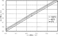
電流―電圧変換部2の薄膜トランジスタを駆動するゲート電圧(これを制御電圧と呼ぶ)としては温度無依存の領域を用いるが、0.3Vはしきい値付近であり、特性の安定が得られないので、飽和領域の12V近傍に制御電圧を設定した。図6は図2(a)において制御電圧を10Vとした場合の入出力電圧特性である。入力電圧2〜8Vの範囲で温度依存性が得られ、5V近傍での温度感受性が最も大きい。入力電圧を5Vに固定した場合の温度に対する出力電圧の変化を図7に示す。出力電圧は温度に対して良好な直線性を示し1ケルビン当たりの電圧上昇値は1.5mVである。ポリシリコン技術で作成したTFTはしきい値のばらつきが大きいが、本実施例ではしきい値より十分に大きいゲート電圧を用いているのでしきい値ばらつきの影響はほとんどない。図2(b)の構成においても、ほぼ同様の結果を得ることができた。また、図2(c)の構成においては制御電圧を10Vとし、温度感知部1のゲート電極に図3において温度依存性が大きいことが確認されている3Vを印加することによって、やはりほぼ同様の結果を得ることができた。
2 Characteristics when using a control voltage that gives a temperature-independent drain current As a gate voltage (referred to as a control voltage) for driving the thin film transistor of the current-
3 温度依存性が温度感知部とは逆のドレイン電流を与える制御電圧を使用した場合の特性
電流−電圧変換部2の制御電圧として、温度依存性が温度感知部1と逆になるしきい値の6倍以上の領域を使用することによっても、温度センサとしての機能を実現できる。一例として図2(c)の構成において、制御電圧を15V、温度感知部1のゲート電圧を3V近傍、入力電圧を5ボルトに設定した場合の温度と出力電圧の関係を図17に示す。電流−電圧変換部2の温度依存性と温度感知部1の温度依存性が図3に示したように、逆の特性となるために、温度依存性が温度感知部1と逆になる温度センサとしての動作が可能である。この場合も出力電圧は温度に対して良好な直線性を示している。1ケルビン当たりの電圧上昇値は3.0mVで、前項の温度無依存のドレイン電流を与える制御電圧を使用した場合に比べて約2倍の高い感度を得ることができる。
3 Characteristics when using a control voltage that gives a drain current whose temperature dependency is opposite to that of the temperature sensing unit As a control voltage of the current-
4 制御電圧の最適化
温度センサとして最適な制御電圧を決定するため、温度感度の制御電圧依存性を調べた。制御電圧としきい値電圧の比を変えた幾つかの条件に対し、5℃の温度変化に対する出力電圧の変化を測定した。結果を図18に示す。横軸は、制御電圧としきい値電圧の比、縦軸は、温度が5℃変化した時の出力電圧の変化(mV/K:ミリボルト/ケルビン)である。制御電圧としきい値電圧の比が2.0の条件は後述する比較例1の条件であり、温度を変えても電圧変化がほとんどない。2.5で電圧変化が若干現れるが、その値は小さく、温度センサとして使用するには不十分である。3.0になると、電圧変化の平均値が0.5mV/K程度となり、温度センサとして実用可能となる。比が3.5では電圧変化の平均値が1.1mV/K程度、比が4.0では電圧変化の平均値が1.5mV/K程度である。このように、制御電圧としきい値電圧の比が3以上になると温度センサとして良好な機能が得られる。制御電圧としきい値電圧の比を変化させる範囲を更に拡大した測定を行い、回帰分析処理することにより、温度感受性との関係をより広い範囲で一般化することができた。この測定では、出力電圧の変化と温度の変化の比の測定温度範囲での平均値をゲインとして定義した。このゲインは、温度を横軸に、出力電圧を縦軸に表し、得られた特性を直線で近似し回帰分析した場合の回帰係数に相当する。また、この回帰分析における決定係数(R2値と呼ばれる)は、回帰直線の回りでの測定値の散らばり度を示す。すなわち、決定係数は、出力電圧の温度に対する直線性を示す。この値は、0から1の範囲を取り、1に近いほど直線性が良い事になる。さて、制御電圧としきい値電圧の比を、0.5、1.0、2.0、2.5、3.0、3.5、4.0、6.0、10.0と変化させた時のゲインと直線性の関係を図19に示す。制御電圧としきい値電圧の比が2.0の場合は、出力電圧値がほぼ一定値となるため、温度を横軸とした回帰分析では正確な決定係数を求められない。そのため、比が2.0での直線性はプロットしていない。図から分かるように、制御電圧としきい値電圧の比が1.0より小さい領域では、非常に直線性が高い特性が得られ、また、比が0.5の場合のように、ある程度のゲインが得られる条件が存在し、温度センサとして使用可能である。しかしながら、この領域は、前述のように、しきい値電圧の影響を大きく受けるため、ポリシリコン技術で使用する場合、測定誤差が大きくなってしまう。比が2.5の時は、ゲインが低く、また、直線性があまり良くない。一方、制御電圧としきい値電圧の比が3.0以上では、ゲインは1ケルビンあたり0.5mV以上となり、また、95%を超える直線性が得られる。このように、比が3.0以上では、ゲイン・直線性共に良好な値を示し、温度センサとして使用が可能である。
4. Optimization of control voltage In order to determine the optimum control voltage as a temperature sensor, the dependence of the temperature sensitivity on the control voltage was examined. The change of the output voltage with respect to the temperature change of 5 ° C was measured for several conditions where the ratio of the control voltage and the threshold voltage was changed. The results are shown in FIG. The horizontal axis represents the ratio between the control voltage and the threshold voltage, and the vertical axis represents the change in output voltage (mV / K: millivolt / Kelvin) when the temperature changes by 5 ° C. The condition where the ratio of the control voltage to the threshold voltage is 2.0 is the condition of Comparative Example 1 described later, and there is almost no voltage change even when the temperature is changed. A voltage change appears slightly at 2.5, but the value is small and insufficient for use as a temperature sensor. At 3.0, the average value of the voltage change is about 0.5 mV / K, making it practical as a temperature sensor. When the ratio is 3.5, the average value of the voltage change is about 1.1 mV / K, and when the ratio is 4.0, the average value of the voltage change is about 1.5 mV / K. Thus, when the ratio of the control voltage and the threshold voltage is 3 or more, a good function as a temperature sensor can be obtained. By performing measurement with a further expansion of the range in which the ratio between the control voltage and the threshold voltage was changed and performing regression analysis, the relationship with temperature sensitivity could be generalized over a wider range. In this measurement, the average value of the ratio between the change in output voltage and the change in temperature in the measured temperature range was defined as the gain. This gain corresponds to a regression coefficient when the temperature is plotted on the horizontal axis and the output voltage is plotted on the vertical axis, and the obtained characteristics are approximated by a straight line and subjected to regression analysis. In addition, the coefficient of determination (referred to as R2 value) in this regression analysis indicates the degree of dispersion of the measured values around the regression line. That is, the determination coefficient indicates linearity of the output voltage with respect to temperature. This value ranges from 0 to 1, and the closer to 1, the better the linearity. FIG. 19 shows the relationship between the gain and linearity when the ratio of the control voltage to the threshold voltage is changed to 0.5, 1.0, 2.0, 2.5, 3.0, 3.5, 4.0, 6.0, 10.0. When the ratio between the control voltage and the threshold voltage is 2.0, the output voltage value is almost constant, so that an accurate determination coefficient cannot be obtained by regression analysis with the temperature as the horizontal axis. Therefore, the linearity at a ratio of 2.0 is not plotted. As can be seen from the figure, in the region where the ratio between the control voltage and the threshold voltage is less than 1.0, a characteristic with very high linearity is obtained, and a condition that a certain degree of gain is obtained as in the case where the ratio is 0.5. Can be used as a temperature sensor. However, since this region is greatly affected by the threshold voltage as described above, a measurement error increases when used in the polysilicon technology. When the ratio is 2.5, the gain is low and the linearity is not so good. On the other hand, when the ratio between the control voltage and the threshold voltage is 3.0 or more, the gain is 0.5 mV or more per Kelvin, and linearity exceeding 95% is obtained. Thus, when the ratio is 3.0 or more, both the gain and linearity show good values and can be used as a temperature sensor.
制御電圧は常時印加する必要は無く、温度情報が必要である周期で、断続的に印加してもよい。このようにすることによって、低消費電力の効果を得ることができる。本発明の温度センサでは、制御電圧を印加すると、入力電圧と負の電源電圧間に電流が流れる。この電流の温度変化を測定することで温度情報を得る。制御電圧の代わりに図2(a)の電流−電圧変換部のトランジスタがオフ状態となる電圧を印加することで、電流―電圧変換部のトランジスタでの電流の流れがほぼ0となる。同時に、温度センサ部分での電流の流れも生じなくなり、ほぼ消費電流が0となる。対象物の温度の変化が例えば、1秒当たり1℃程度である場合、1秒に一回の測定でも、十分な温度情報が得られる。例えば、1秒間に一回10ミリ秒の期間に温度測定をする場合、このような制御電圧の断続的な印加方法を使えば電流消費を100分の一にする事が出来る。実際は、オフ時のリーク電流並びに、制御電圧部に印加する電圧を変化させる事による電流消費が存在するために、25分の一程度の消費電流となる。 The control voltage need not always be applied, and may be intermittently applied at a period where temperature information is required. By doing so, an effect of low power consumption can be obtained. In the temperature sensor of the present invention, when a control voltage is applied, a current flows between the input voltage and the negative power supply voltage. Temperature information is obtained by measuring the temperature change of the current. By applying a voltage that turns off the transistor of the current-voltage conversion unit in FIG. 2A instead of the control voltage, the current flow in the transistor of the current-voltage conversion unit becomes almost zero. At the same time, no current flows in the temperature sensor portion, and the current consumption becomes almost zero. When the change in the temperature of the object is, for example, about 1 ° C. per second, sufficient temperature information can be obtained even with one measurement per second. For example, when the temperature is measured once per second for a period of 10 milliseconds, the current consumption can be reduced to 1/100 by using such an intermittent application method of the control voltage. Actually, the current consumption is about 1/25 because the leakage current at the off time and the current consumption by changing the voltage applied to the control voltage unit exist.
5 温度センサによる駆動制御
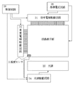
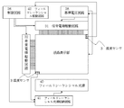
図26に、温度センサで得られた温度情報を、液晶表示装置駆動回路の基準電圧にフィードバックする機能ブロックの一例を示す。液晶表示部は信号電極駆動回路31と走査電極駆動回路32によって駆動される。これらは制御回路36でその動作が制御されている。信号電極駆動回路31が発する信号は基準電圧回路35で発生した基準電圧によってその振幅が決定される。液晶表示部には本発明の温度センサ3が配設され、温度センサ3からの出力信号によって基準電圧35の信号振幅が制御される。その結果として液晶に実際に印加する信号電圧の振幅を温度に応じて調整することが可能となるので、温度に依存しない画像品質を得ることができる。この温度情報で調整された基準電圧は、基準電圧回路35から液晶表示部並びに信号電極駆動回路31に印加され、その結果として液晶に実際に印加する信号電圧の振幅を温度に応じて調整する事が可能となる。同様に、図27のように、温度センサ3から出力された温度情報を、バックライトにフィードバックする事も可能である。画面を明るくするために、液晶表示装置では液晶表示部を光源33から放射される光で照らす。光源33は制御回路36で駆動される光源駆動回路34で光源輝度を調整する。液晶表示部に配設された温度センサ3の出力電圧を光源駆動回路34にフィードバックすることにより温度変化に応じて光源輝度を調整することが可能となる。この構成では、例えば低温になって液晶表示部の光利用効率が低下する場合、バックライトの輝度を上げる制御を行うことによって、温度低下の表示に与える影響を抑制することができる。
5 Drive Control by Temperature Sensor FIG. 26 shows an example of a functional block that feeds back temperature information obtained by the temperature sensor to the reference voltage of the liquid crystal display device drive circuit. The liquid crystal display unit is driven by a signal electrode drive circuit 31 and a scan
6 TFTの製造方法
この実施形態では、もっとも広く利用されている、ポリシリコン技術によるTFTの製法について説明する。ここで、ポリシリコン技術とは、基板上に絶縁膜を介し多結晶構造を有するポリシリコン薄膜を形成する技術をいう。
6 TFT Manufacturing Method In this embodiment, the most widely used TFT manufacturing method using polysilicon technology will be described. Here, the polysilicon technique refers to a technique for forming a polysilicon thin film having a polycrystalline structure on a substrate via an insulating film.
(1)基本的作成方法
TFTの構造にはトップゲート型とボトムゲート型の2種類がある。まず、トップゲート型のTFTを適用した場合について図15を用いて説明する。ガラス基板29上に酸化シリコン膜28を形成した後、アモルファスシリコンを成長させた。次にエキシマレーザを用いアニールしアモルファスシリコンをポリシリコン27に改質し、パターニングした後、更に10nmの酸化シリコン膜28を成長させた。フォトレジストをゲート形状より若干大きく(後にLDD領域23、24を形成するため)パターニングし、リンイオンをドーピングすることによりソース領域とドレイン領域を形成した。その後、ゲート酸化膜となる酸化シリコン膜28を成長させた後、ゲート電極となるアモルファスシリコンとタングステンシリサイド(WSi)を成長させ、フォトレジストをマスクとしてこれをパターニングし、ゲート電極を形成した。更に、パターニングしたフォトレジストをマスクとして必要領域にのみリンイオンをドーピングすることによりLDD領域23、24を形成した。その後、酸化シリコン膜28と窒化シリコン膜21を連続成長させた後、コンタクト用の穴をあけ、アルミニウムとチタンをスパッタで形成した後パターニングしソース電極26、ドレイン電極25を形成した。その後、全面に窒化シリコン膜21を形成し、コンタクト用の穴をあけ、全面にITO膜を形成し、パターニングすることで透明な画素電極22を形成した。
(1) Basic production method There are two types of TFT structures, a top gate type and a bottom gate type. First, the case where a top gate type TFT is applied will be described with reference to FIG. After the silicon oxide film 28 was formed on the glass substrate 29, amorphous silicon was grown. Next, annealing was performed using an excimer laser to modify the amorphous silicon into polysilicon 27, and after patterning, a 10 nm silicon oxide film 28 was further grown. The photoresist was patterned slightly larger than the gate shape (to form
このようにして図15に示すようなプレーナ型のTFT画素スイッチを作成し、TFTアレイを形成することで、ガラス基板上にTFTスイッチによる画素アレイ並びに走査回路を設けた。なお、アレイ化に関しては従来通りの製法で作成できる。図15では、アモルファスシリコンをポリシリコン化したTFTを形成しているが、ポリシリコンを成長後、レーザ照射によりポリシリコンの粒径を改善する方法でTFTを形成しても良い。また、レーザはエキシマレーザ以外にも連続発振(CW)レーザを用いても良い。 In this way, a planar TFT pixel switch as shown in FIG. 15 was prepared and a TFT array was formed, so that a pixel array and a scanning circuit by the TFT switch were provided on the glass substrate. It should be noted that the array can be created by a conventional manufacturing method. In FIG. 15, a TFT in which amorphous silicon is made into polysilicon is formed. However, after growing the polysilicon, the TFT may be formed by a method of improving the grain size of polysilicon by laser irradiation. In addition to the excimer laser, a continuous wave (CW) laser may be used as the laser.
(2)温度センサ作成方法
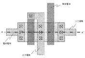
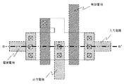
(1)で説明した工程を基本として本発明の温度センサを作成することができる。ここで用いたマスクレイアウト図の一例を図20に示す。また、このマスクを用いて作成した素子の図20の線A−A’での断面図を図21に示す。この例では、温度感知部のゲート電極、ドレイン電極、及び電流−電圧変換部のソース電極は出力電極の金属を介して接続されダイオードと等価となる。また他のマスクレイアウトの例を図22に、このマスクを用いて作成した素子のB−B’での断面図を図23に示す。この例では、温度感知部のゲート電極、ドレイン電極、及び電流−電圧変換部のソース電極は出力電極の金属材料ではなくポリシリコン膜を介して接続される。この構造では、ダイオード接続部分には、ゲート電極とドーピングされたポリシリコン膜との間のコンタクトのみが存在する。
(2) Temperature sensor creation method The temperature sensor of the present invention can be created based on the process described in (1). An example of the mask layout diagram used here is shown in FIG. Further, FIG. 21 shows a cross-sectional view taken along line AA ′ of FIG. 20 of an element formed using this mask. In this example, the gate electrode and drain electrode of the temperature sensing unit, and the source electrode of the current-voltage conversion unit are connected via the metal of the output electrode and are equivalent to a diode. Another example of the mask layout is shown in FIG. 22, and a cross-sectional view taken along the line BB ′ of an element formed using this mask is shown in FIG. In this example, the gate electrode and drain electrode of the temperature sensing unit and the source electrode of the current-voltage conversion unit are connected via a polysilicon film instead of the metal material of the output electrode. In this structure, only the contact between the gate electrode and the doped polysilicon film exists in the diode connection portion.
なお、ここまでの説明はゲート電極を薄膜半導体層より上部に有するトップゲート型TFTに関して行ったが、ゲート電極を薄膜半導体層より下側に有するボトムゲート型TFTでも本発明は実現できる。ボトムゲート型のTFTを使った場合の本発明の温度センサの製法について説明する。図24はボトムゲート型TFTによる本発明の実施例の素子の断面図である。ゲート電極が最下層となっている点以外は、図20図21で説明した温度感知部のゲート電極、ドレイン電極及び電流−電圧変換部のソース電極を出力電極の金属を介して接続する温度センサのレイアウトと同様である。また、図25に、図24の製造方法のうち、ソース・ドレイン領域の作製方法を示す。ガラス基板29上に酸化シリコン(不図示)を堆積し、その上にクロミウム(Cr)をゲート電極30として形成する。続いてPE−CVD法により窒化シリコン膜21、または酸化シリコン膜28をゲート絶縁膜として形成し、連続してアモルファスシリコン12を成膜した。アモルファスシリコン12のチャネル領域上にドーピング用マスクとしてのフォトレジスト14のパターンを形成し、イオンドーピング法により不純物(リンもしくはボロンなど)をソース・ドレイン領域に注入した(a)。フォトレジスト14を除去し、アモルファスシリコン膜12の水素濃度を低減するために真空中で400℃、90分の加熱処理を行い、エキシマレーザを照射しアモルファスシリコン膜12を結晶化した(b)。不純物をドーピングした領域は結晶化と同時に活性化された。ソース・ドレイン電極を形成した後、酸化シリコン膜を堆積し、poly-Si薄膜の粒界に存在するダングリングボンドを減らすために300℃の水素プラズマ雰囲気中で90分間の水素化処理を行い、TFTを作製した。
Although the description so far has been made with respect to the top gate type TFT having the gate electrode above the thin film semiconductor layer, the present invention can be realized even with the bottom gate type TFT having the gate electrode below the thin film semiconductor layer. A manufacturing method of the temperature sensor of the present invention when a bottom gate type TFT is used will be described. FIG. 24 is a cross-sectional view of an element according to an embodiment of the present invention using a bottom gate TFT. A temperature sensor that connects the gate electrode, drain electrode, and source electrode of the current-voltage conversion unit described with reference to FIG. 20 through the metal of the output electrode except that the gate electrode is the lowest layer. The layout is the same. FIG. 25 shows a method for manufacturing a source / drain region in the manufacturing method of FIG. Silicon oxide (not shown) is deposited on the glass substrate 29, and chromium (Cr) is formed thereon as the
以上、本発明の第一の実施の形態では、制御電圧として印加する電圧を適当な範囲に設定することによって、温度感知部1で検出した温度変化による電流変化を、電流−電圧変換部2において電圧変化として検出することが可能である。制御電圧を、ドレイン電流が温度依存性を生じない領域、または、温度感知部の温度依存性と異なる領域に設定することによって、電流−電圧変換部2と温度感知部1は温度に対して独立した特性を示すことができ、良好な温度センサを構成することができる。
As described above, in the first embodiment of the present invention, the current applied due to the temperature change detected by the
(第2の実施の形態)
本実施の形態は、TFT形成をポリシリコン技術ではなく、部分空乏型SOI技術で作成する点が第1の実施の形態と異なる。SOI技術とは、基板上に絶縁膜を介し単結晶シリコン薄膜を形成する技術をいう。SOI技術は、部分空乏型SOI技術と、完全空乏型SOI技術に分けられる。両者の違いはシリコン膜内の空乏化の程度であり、具体的にはシリコン膜の厚みで分けられる。シリコン膜の厚みが、空乏層の最大の厚みの2倍より大きい場合のプロセスを部分空乏型SOI技術と呼ぶ。空乏層の最大の厚みは、不純物量やフェルミポテンシャル等に依存し、デバイス技術毎に異なっている。そのため、部分空乏型と完全空乏型のシリコン膜厚もデバイス技術毎に異なるが、50nmより小さい場合を、完全空乏型、100nmから200nm(もしくは、それ以上)の場合を部分空乏型と呼ぶ事が一般的である。したがって、ここでもそのように定義する。SOI技術は、バルクシリコン技術に比べて、(1)接合容量が小さいため低電圧・高速動作が可能である、(2)放射線に対する耐性が高い、(3)クロストークが少なく回路を密に集積できる、等の特徴がある。SOI技術用の基板は、現在、酸素イオン注入によるSIMOX基板、水素イオンと貼り合わせ・剥離によるUNIBOND(Smart Cut)基板、多孔質シリコン基板を用いた貼り合わせとウォータージェット分離によるELTRAN基板等が製品化されている。部分空乏型SOIは、シリコン基板が異なるだけで、デバイスを作成するプロセスは、通常のバルクシリコンと同じプロセスが使用できる。部分空乏型SOIでは、貼り合わせによる基板がよく用いられる。貼り合わせ基板では、酸化膜の厚みが精度良く制御される。また、機械的に研磨等が行われ膜厚が変動しやすいシリコン部分は、部分空乏型の膜厚が厚いため、膜厚の変動の影響が少ない。この二つの理由から、貼り合わせ基板がよく用いられている。なお、シリコン膜の厚みが空乏層の最大の厚みより小さい場合のプロセスは完全空乏型SOI技術と呼ぶ。これに関しては第3の実施形態において説明する。
(Second Embodiment)
This embodiment is different from the first embodiment in that the TFT is formed not by polysilicon technology but by partially depleted SOI technology. SOI technology refers to a technology for forming a single crystal silicon thin film on a substrate via an insulating film. SOI technology is divided into partially depleted SOI technology and fully depleted SOI technology. The difference between the two is the degree of depletion in the silicon film, and is specifically divided by the thickness of the silicon film. A process in which the thickness of the silicon film is larger than twice the maximum thickness of the depletion layer is called a partially depleted SOI technology. The maximum thickness of the depletion layer depends on the amount of impurities, Fermi potential, etc., and differs for each device technology. For this reason, the film thicknesses of partially depleted and fully depleted silicon differ depending on the device technology. However, when the thickness is less than 50 nm, the case where the thickness is less than 50 nm is called the fully depleted type, and the case of 100 to 200 nm (or more) is called the partially depleted type. It is common. Therefore, this is also defined here. Compared with bulk silicon technology, SOI technology (1) has low junction capacitance and can operate at low voltage and high speed. (2) High resistance to radiation. (3) Less crosstalk and dense circuit integration. There are features such as being able to. SOI technology substrates currently include SIMOX substrates by oxygen ion implantation, UNIBOND (Smart Cut) substrates by bonding and peeling with hydrogen ions, ELTRAN substrates by bonding and water jet separation using porous silicon substrates, etc. It has become. Partially depleted SOI differs only in the silicon substrate, and the same process as that for normal bulk silicon can be used to fabricate the device. In partially depleted SOI, a bonded substrate is often used. In the bonded substrate, the thickness of the oxide film is controlled with high accuracy. In addition, since the silicon portion that is mechanically polished or the like and easily changes in film thickness is thick in a partial depletion type, the influence of the film thickness variation is small. For these two reasons, bonded substrates are often used. A process in which the thickness of the silicon film is smaller than the maximum thickness of the depletion layer is referred to as a fully depleted SOI technology. This will be described in the third embodiment.
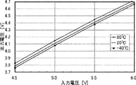
図4に部分空乏型SOI技術で作成したTFTのドレイン電流−ゲート電圧依存性の一例を示す。図3のポリシリコン技術と比べると、SOI技術の半導体層の移動度は10倍近く高く、且つ、ポリシリコンで見られるような結晶粒界でのトラップ現象が無い事に加え、本実施例ではLDD構造を用いなかったために、ドレイン電流は図3より二桁近く上昇している。前述のように、横軸はゲート電圧、縦軸は対数表示でのドレイン電流であり、温度を−40℃、20℃、80℃と変えた場合、ゲート電圧1.9V近辺と、ゲート電圧が12V近辺で温度によるドレイン電流が温度無依存となる領域が存在する。図8は制御電圧を12Vとした場合の図2(a)の構造の温度センサにおける入力電圧―出力電圧特性である。ポリシリコン技術と比べると、温度への感受性はかなり低く、1ケルビン当たりの電圧上昇値は0.5mVではあったが、部分空乏型SOI技術においても、本発明の温度センサが実現できた。 FIG. 4 shows an example of the drain current-gate voltage dependency of a TFT produced by the partially depleted SOI technology. Compared to the polysilicon technology of FIG. 3, the mobility of the semiconductor layer of the SOI technology is nearly 10 times higher and there is no trapping phenomenon at the crystal grain boundary as seen in polysilicon, Since the LDD structure is not used, the drain current rises nearly two orders of magnitude from FIG. As described above, the horizontal axis represents the gate voltage, the vertical axis represents the logarithmic drain current, and when the temperature is changed to −40 ° C., 20 ° C., and 80 ° C., the gate voltage is around 1.9 V and the gate voltage is There is a region where the drain current due to temperature becomes temperature-independent around 12V. FIG. 8 shows the input voltage-output voltage characteristics in the temperature sensor having the structure of FIG. 2A when the control voltage is 12V. Compared with the polysilicon technology, the sensitivity to temperature is considerably low, and the voltage increase value per Kelvin was 0.5 mV, but the temperature sensor of the present invention could be realized even in the partially depleted SOI technology.
(第3の実施の形態)
本実施の形態は、TFTの形成をポリシリコン技術ではなく、完全空乏型SOI技術で作成する点が第1、第2の実施の形態と異なる。完全空乏型SOI技術とは、シリコン膜の厚みが空乏層の最大の厚みより小さい場合のSOI技術を言い、一般的にその厚みは50nm以下である。(完全空乏型SOI技術により、電流−電圧変換部は、ゲート電極に基板方向から印加する電圧(以降バックゲート電圧と呼ぶ)を調整する事によってボディ領域底部を擬似的に空乏化していない状態にしている。また、このバックゲート電圧を印加する電極のことをここではバックゲート電極と呼ぶ。この構造により、完全空乏型SOI技術の空乏化したチャネルのバックゲート側を、空乏化していない状態にする事が可能となる。)図5に完全空乏型SOI技術で作成したTFTのドレイン電流−ゲート電圧依存性の一例を示す。図3のポリシリコン技術と比べると、高いドレイン電流が得られている。前述のように、横軸はゲート電圧、縦軸は対数表示でのドレイン電流であり、温度を−40℃、20℃、80℃と変えた場合、ゲート電圧1.9V近辺と、ゲート電圧が12V近辺で温度によるドレイン電流が温度無依存となる領域が存在し、部分空乏化型SOI技術とほとんど変わらない結果が得られた。図9は制御電圧を12Vとした場合の図2(a)の構造の温度センサにおける入力電圧―出力電圧特性である。1ケルビン当たりの電圧上昇値は0.6mVで部分空乏型SOI技術に比べるとやや高い温度感受性が得られた。ポリシリコン技術に比べると感度は低いものの、完全空乏型SOI技術においても本発明の温度センサが実現できた。
(Third embodiment)
This embodiment is different from the first and second embodiments in that the TFT is formed not by polysilicon technology but by fully depleted SOI technology. The fully depleted SOI technology refers to an SOI technology in which the thickness of the silicon film is smaller than the maximum thickness of the depletion layer, and generally the thickness is 50 nm or less. (By using the fully depleted SOI technology, the current-voltage conversion unit adjusts the voltage applied to the gate electrode from the substrate direction (hereinafter referred to as the back gate voltage) so that the bottom of the body region is not pseudo-depleted. In addition, an electrode to which the back gate voltage is applied is referred to as a back gate electrode, and this structure makes the back gate side of the fully depleted SOI technology depleted channel undepleted. FIG. 5 shows an example of the drain current-gate voltage dependency of a TFT formed by the fully depleted SOI technology. Compared with the polysilicon technology of FIG. 3, a higher drain current is obtained. As described above, the horizontal axis represents the gate voltage, the vertical axis represents the logarithmic drain current, and when the temperature is changed to −40 ° C., 20 ° C., and 80 ° C., the gate voltage is around 1.9 V and the gate voltage is In the vicinity of 12V, there is a region where the drain current due to temperature becomes temperature-independent, and the result is almost the same as that of the partially depleted SOI technology. FIG. 9 shows input voltage-output voltage characteristics in the temperature sensor having the structure of FIG. 2A when the control voltage is 12V. The voltage rise per Kelvin was 0.6 mV, which was a little higher temperature sensitivity than the partially depleted SOI technology. Although the sensitivity is lower than that of the polysilicon technology, the temperature sensor of the present invention can be realized even in the fully depleted SOI technology.
第2、第3の実施の形態と比較すると、LDD構造を用いたポリシリコン技術による第一の実施の形態は、1.SOI技術に比べ温度感受性が高い事、2.より低電流の領域で温度依存のない特性が得られ低消費電力である事、から、温度センサとして最も良好であると考えられる。通常、ポリシリコン技術による回路では、しきい値のばらつきが問題となるが、本発明では、しきい値電圧の3倍以上の領域を使用するので、しきい値の影響を極めて受けにくい。 Compared with the second and third embodiments, the first embodiment by the polysilicon technology using the LDD structure is as follows. 1. High temperature sensitivity compared to SOI technology. Since a temperature-independent characteristic is obtained in a lower current region and the power consumption is low, it is considered to be the best temperature sensor. Usually, in a circuit using polysilicon technology, variation in threshold value becomes a problem. However, in the present invention, since a region of three times or more of the threshold voltage is used, it is hardly affected by the threshold value.
(第4の実施の形態)
本実施の形態は、第1の実施の形態において、温度センサの出力電圧取り出し部に増幅器を接続するものである。
(Fourth embodiment)
In the present embodiment, an amplifier is connected to the output voltage extraction unit of the temperature sensor in the first embodiment.
作製した増幅部の回路構成を、図10に示す。この増幅部は、カレントミラー回路と差動入力回路を用いたオペレーショナル・トランスコンダクタンス・アンプ(OTA)構成である。本実施の形態では差動対による基本的な増幅回路について説明するが、他の増幅回路を用いても構わない。この図10の増幅部では、トランジスタを7個使用している。全てのトランジスタは、ゲート長を4ミクロンとした。トランジスタT1、T2、T5、T6はpチャンネル薄膜トランジスタであり、トランジスタT3,T4,T7はnチャンネル薄膜トランジスタである。ゲート幅は、T1とT2が7ミクロン、T3とT4が11ミクロン、T5が22ミクロン、T6とT7は75ミクロンとした。また、補償容量Cfは35フェムトファラド(35fF)とした。補償容量は、ゲート電極線とデータ電極線の各々と同層の金属で作製し、この間の酸化膜の膜厚は4000オングストロームとし、容量の電極のサイズは縦65ミクロン、横6ミクロンとした。この増幅部は、1ピコファラド(1pF)の負荷を接続した場合に、40dB(デシベル)のゲインが得られた。 FIG. 10 shows a circuit configuration of the manufactured amplification unit. This amplification unit has an operational transconductance amplifier (OTA) configuration using a current mirror circuit and a differential input circuit. In this embodiment, a basic amplifier circuit using a differential pair is described, but other amplifier circuits may be used. In the amplifying unit in FIG. 10, seven transistors are used. All transistors had a gate length of 4 microns. Transistors T1, T2, T5, and T6 are p-channel thin film transistors, and transistors T3, T4, and T7 are n-channel thin film transistors. The gate width was 7 microns for T1 and T2, 11 microns for T3 and T4, 22 microns for T5, and 75 microns for T6 and T7. The compensation capacitance Cf was 35 femtofarad (35 fF). The compensation capacitance was made of the same metal layer as each of the gate electrode line and the data electrode line, the thickness of the oxide film between them was 4000 angstroms, and the size of the capacitance electrode was 65 microns long and 6 microns wide. When this amplifying unit was connected to a load of 1 picofarad (1 pF), a gain of 40 dB (decibel) was obtained.
この図10による増幅部と、図2の温度感知部1と電流−電圧変換部2を出力電圧端子と差動入力端子で接続する事で、温度センサを構成した。温度感知部1と電流−電圧変換部2、ゲート長4ミクロン、ゲート幅12ミクロンで作製した。図10に示す正の電源電圧線には10Vを印加し、負の電源電圧線は接地した。
A temperature sensor is configured by connecting the amplification unit shown in FIG. 10 and the
この温度センサは、定電流源に相当するトランジスタT5とT6に印加するバイアス電圧の大きさによって、特性が変化する。バイアス電圧を変えた時の、温度センサの増幅部の出力電圧を測定した結果を図11に示す。温度を−40℃、20℃、80℃と変えた場合、バイアス電圧9.8V近傍で、出力電圧の温度依存性がもっとも顕著になることが分かる。この結果に基づき、バイアス電圧を9.75Vとした時の増幅部の出力電圧の温度依存性を測定した。結果を図12に示す。温度は、−40℃から80℃まで5℃刻みで変化させた。温度に対し比較的良好な直線性が得られ、1ケルビン当たりの電圧上昇値は8ミリボルト程度であり、増幅部を有さない第1の実施の形態に比べて、約5倍の振幅の出力が得られている。 The characteristics of this temperature sensor change depending on the magnitude of the bias voltage applied to the transistors T5 and T6 corresponding to the constant current source. FIG. 11 shows the result of measuring the output voltage of the amplification unit of the temperature sensor when the bias voltage is changed. It can be seen that when the temperature is changed to −40 ° C., 20 ° C., and 80 ° C., the temperature dependence of the output voltage becomes most noticeable in the vicinity of the bias voltage of 9.8V. Based on this result, the temperature dependence of the output voltage of the amplifier when the bias voltage was 9.75 V was measured. The results are shown in FIG. The temperature was changed from −40 ° C. to 80 ° C. in increments of 5 ° C. A relatively good linearity with respect to the temperature is obtained, the voltage rise value per Kelvin is about 8 millivolts, and an output having an amplitude about 5 times that of the first embodiment having no amplification unit. Is obtained.
(第5の実施の形態)
本発明の第6の実施の形態は、無線周波数を利用して認識を行うRF−ID素子であって、本発明の温度センサを内蔵したRF−ID素子である。RF−ID(Radio Frequency IDentification)素子の通信方式並びに周波数帯には様々な方式がある。例を挙げると、マイクロ波を用いるマイクロ波方式、数十キロヘルツから数十メガヘルツ帯を用いる電磁誘導方式、数百キロヘルツ帯を用いる電磁結合方式等がある。本発明ではRF−ID素子に温度センサを内蔵する事により、RF−ID素子内で、温度による素子の動作の変動の補償が可能となる。一方、RF−ID素子もしくはRF−ID素子を取り付けた物体の温度を、外部から非接触でモニタする事が出来る。
(Fifth embodiment)
The sixth embodiment of the present invention is an RF-ID element that performs recognition using a radio frequency, and is an RF-ID element incorporating the temperature sensor of the present invention. There are various communication systems and frequency bands of RF-ID (Radio Frequency IDentification) elements. For example, there are a microwave system using microwaves, an electromagnetic induction system using several tens of kilohertz to several tens of megahertz, and an electromagnetic coupling system using several hundreds of kilohertz. In the present invention, by incorporating a temperature sensor in the RF-ID element, it is possible to compensate for fluctuations in the operation of the element due to temperature in the RF-ID element. On the other hand, the temperature of the RF-ID element or the object to which the RF-ID element is attached can be monitored from the outside without contact.
(第6の実施の形態)
本発明の第7の実施の形態は、本発明の温度センサを備えるバイオチップにもしくはDNAチップである。バイオチップは、光学式、電子式と大きく分けられている。光学式バイオチップでは既知の遺伝子から得られたDNA断片(プローブ)が、決められた位置に正確に配置され基板に化学的に結合されている。鍵と鍵穴の関係で評価試料中の対応する部分が結合し、発光染料などのマーカー手段によって発光させ、CCD等で検出する。電子式バイオチップでは、検査対象の物質は酵素でマーキングし、電気的に活性な2つの部分に分離し、生じた電流を金等の電極を備えるセンサで検出する。電流の時間変化から、対象物質の濃度を知る。ポリシリコン技術によれば、光学式ならびに電子式のおのおのの方式を安価に実現できるだけでなく、双方を融合したバイオチップも実現可能である。本発明の温度センサをバイオチップ上に形成すれば、作成されたバイオチップの分析時の温度を正確にモニタすることができ、解析精度を高めることができる。また、本発明の温度センサを備えることにより、反応が生じている部位の温度を正確に知ることが出来、生体観察において有用なデータを取得することができる。
(Sixth embodiment)
The seventh embodiment of the present invention is a biochip or a DNA chip including the temperature sensor of the present invention. Biochips are broadly divided into optical and electronic types. In an optical biochip, a DNA fragment (probe) obtained from a known gene is accurately arranged at a predetermined position and chemically bonded to a substrate. Corresponding portions in the evaluation sample are combined due to the relationship between the key and the keyhole, light is emitted by marker means such as a luminescent dye, and detected by a CCD or the like. In an electronic biochip, a substance to be inspected is marked with an enzyme, separated into two electrically active parts, and the generated current is detected by a sensor having an electrode such as gold. Know the concentration of the target substance from the change in current over time. According to the polysilicon technology, not only the optical and electronic systems can be realized at low cost, but also a biochip that combines both can be realized. If the temperature sensor of the present invention is formed on a biochip, the temperature at the time of analysis of the produced biochip can be accurately monitored, and the analysis accuracy can be increased. Moreover, by providing the temperature sensor of the present invention, it is possible to accurately know the temperature of the site where the reaction occurs, and it is possible to acquire useful data in living body observation.
DNAチップはバイオチップの1種として位置づけられることが多いが、市場規模が大きいため別のものとして分類されることもある。DNAチップの多くは蛍光分析の必要性等から、シリコン基板を用いるよりスライドガラス等のガラス基板を用いることが望まれる。DNAチップは通常、フォトリソグラフィ技術を利用して基板上で逐次、プローブを合成するため、非常に高価となっている。更に、ガラス基板を用いると、電気的な検査をする場合は、特殊な配線技術が必要であり、回路等を付加的に作りこむことは困難である。一方、ポリシリコン技術を応用すると、ガラス基板やプラスチック基板を使用できるため、蛍光分析等に対応できると共に、プローブとガラス基板の間に、配線や回路を作りこむことが出来るため、DNAチップを非常に高性能化することができる。プローブの作製には、インクジェット技術(もしくはバブルジェット(登録商標)技術)を応用しDNAインク溶液を印刷することや、マイクロセラミックスポンプによってスポットすることで、安価に作成すること出来る。これにより、ポリシリコン技術によるDNAチップは、従来の10分の1以下の価格で、電気回路も有するきわめて高性能なチップを提供できる。本発明の温度センサをバイオチップに適用すれば、DNA分析の反応時の温度を正確にモニタできるので、DNA解析の精度を向上させられる。 A DNA chip is often positioned as a kind of biochip, but is sometimes classified as another because of its large market size. In many DNA chips, it is desired to use a glass substrate such as a slide glass rather than a silicon substrate because of the necessity of fluorescence analysis. A DNA chip is usually very expensive because a probe is sequentially synthesized on a substrate using a photolithographic technique. Further, when a glass substrate is used, a special wiring technique is required for electrical inspection, and it is difficult to additionally make a circuit or the like. On the other hand, if polysilicon technology is applied, glass substrates and plastic substrates can be used, so it can be used for fluorescence analysis and wiring and circuits can be created between the probe and the glass substrate. High performance can be achieved. The probe can be produced at low cost by applying an ink jet technique (or bubble jet (registered trademark) technique) and printing a DNA ink solution or spotting with a microceramic pump. Thereby, the DNA chip based on the polysilicon technology can provide an extremely high-performance chip having an electric circuit at a price less than one-tenth of the conventional price. If the temperature sensor of the present invention is applied to a biochip, the temperature during the reaction of DNA analysis can be accurately monitored, so that the accuracy of DNA analysis can be improved.
(第7の実施の形態)
本実施の形態は、本発明の温度センサを液晶表示装置のオーバードライブ駆動に適用したものである。その機能ブロック図を図28に示す。本発明を液晶表示装置におけるオーバードライブ駆動に適用した機能ブロック図を図28に示す。基本的な構成は第1の実施の形態で説明した図27と同じであるが、制御回路にオーバードライブ回路を接続している点が異なっている。オーバードライブとは液晶に通常の駆動時より高い電圧を印加して電界強度を増大させ、状態変化を促進させるものであり、液晶駆動の高速化に有効とされている。この例では、光源へのフィードバックも行っている。また、図29に図28のオーバードライブ回路内の機能ブロックの一例を示す。図29においてオーバードライブ回路では、入力信号をフレームバッファ38に蓄えると共に、1フレーム前の信号をフレームバッファ38から読み出し、現在の入力信号と比較する。比較した結果を用い、LUT(ルックアップテーブル)39からオーバードライブ後の映像信号レベルを読み出し、実際に印加する電圧を決定し、出力信号として出力する。図28において温度センサ3を用いた温度情報に基づく補正は、基準電圧回路35とオーバードライブ回路37の双方に入力され、温度に応じた電圧補正が行われる。一方、光源33を駆動する光源駆動回路34にも温度センサ3からの温度情報をフィードバックし、光源の輝度や発光タイミングの調整を行う。本実施例では温度センサ3として、電流−電圧変換部の制御電圧を10V、入力電圧を5Vとした。
(Seventh embodiment)
In this embodiment, the temperature sensor of the present invention is applied to overdrive driving of a liquid crystal display device. The functional block diagram is shown in FIG. FIG. 28 shows a functional block diagram in which the present invention is applied to overdrive driving in a liquid crystal display device. The basic configuration is the same as that of FIG. 27 described in the first embodiment, except that an overdrive circuit is connected to the control circuit. Overdrive is a method in which a higher voltage is applied to the liquid crystal than during normal driving to increase the electric field strength and promote state change, and is effective for speeding up the liquid crystal driving. In this example, feedback to the light source is also performed. FIG. 29 shows an example of functional blocks in the overdrive circuit of FIG. In the overdrive circuit shown in FIG. 29, the input signal is stored in the frame buffer 38, and the previous frame signal is read from the frame buffer 38 and compared with the current input signal. Using the comparison result, the video signal level after overdrive is read from the LUT (lookup table) 39, the voltage to be actually applied is determined, and output as an output signal. In FIG. 28, the correction based on the temperature information using the
また、オーバードライブ方式において、容量予測を行う場合は、図29のオーバードライブ回路の代わりに、図30のオーバードライブ回路を用いる。この回路では、入力信号と、容量用フレームバッファ45から読み出した1フレーム前の各画素の容量とから、容量予測用LUT(ルックアップテーブル)44を用いて、次のフレームの予測容量を決定する。予測容量は、容量用フレームバッファ45に蓄積されると共に、電圧用LUT(ルックアップテーブル)43で入力信号と比較し、実際に印加する信号を決定し、出力信号として出力する。この回路を用いる事により、液晶の応答が遅い等の理由によって所望の輝度が得られない場合に、所望の輝度に対応する必要な液晶容量に所望の時間内に達するように印加電圧を調整する事が可能となる。この結果、オーバードライブ駆動が実現できる。
In the overdrive system, when capacity prediction is performed, the overdrive circuit shown in FIG. 30 is used instead of the overdrive circuit shown in FIG. In this circuit, the predicted capacity of the next frame is determined using the capacity prediction LUT (Look Up Table) 44 from the input signal and the capacity of each pixel one frame before read from the
液晶の応答は温度の影響を受ける。そこで、この電圧用LUTを代表的な温度毎に用意し、測定された温度に応じて電圧用LUTを選択した。この構造により、オーバードライブ回路内での温度に応じた電圧補正を行った。 The response of the liquid crystal is affected by temperature. Therefore, this voltage LUT is prepared for each representative temperature, and the voltage LUT is selected according to the measured temperature. With this structure, voltage correction according to the temperature in the overdrive circuit was performed.
(第8の実施の形態)
本発明をカラーフィールドシーケンシャル方式(色時分割)の液晶表示装置の駆動に適用した例を示す。カラーフィールドシーケンシャル方式では、液晶の応答に使用できる時間が極めて短いために、温度が低下した場合の液晶の応答速度の低下の影響が大きい。本実施例では、温度センサにより温度をモニタし、低温でオーバードライブ電圧の上昇と、バックライト輝度の向上を行う事によって、温度に依存しない良好な表示を得た。フィールドシーケンシャル方式の液晶表示装置における温度情報によるフィードバックを与える場合の機能ブロックの一例を図31に示す。基本的な構成は第1の実施の形態で説明した図27と同じであるが制御回路36にフィールドシーケンシャル駆動回路42を接続し、光源としてフィールドシーケンシャル光源40を用いる点が異なっている。フィールドシーケンシャルカラー方式では、表示画像をいくつかの色の画像に分割し、これを時系列で表示し、且つ、これと同期して画像と同色の光源を点灯する。フィールドシーケンシャル光源40としては複数の波長帯のLED、EL、冷陰極管等を用いることができる。 フィールドシーケンシャル光源駆動回路41は制御回路36で駆動され、フィールドシーケンシャル光源40の色を高速で切り換える機能を持つ。図14にフィールドシーケンシャル表示システムの一例をより詳細に示した。画像データ110を、フィールドシーケンシャルコントローラIC103で処理することによって赤・青・緑の色毎の画像データに変換する。フィールドシーケンシャルコントローラIC103は内部に制御回路36、パルスジェネレータ104、高速フレームメモリ106を有する。画像データ110は一旦高速フレームメモリに蓄えられた上で各色毎に分解され、各々の色の情報に基づいてLED101を駆動するLED制御信号108が制御回路36から発せられる。また、これと同時に制御回路36はパルスジェネレータ104をも駆動し、駆動パルス109を発生させる。画像データ110はDAC(デジタルアナログコンバータ)102を介してLCD100に入力され、LCD100は駆動パルス109を受けて、各色の画像を点灯させる。通常の画像データを制御回路36、パルスジェネレータ104、高速フレームメモリ106を内蔵するフィールドシーケンシャルコントローラIC103で処理する事によって、赤・青・緑の色毎の画像データに変換する。この画像データをDAC102を介して、LCD(液晶表示パネル)100に入力する。LCD100内の走査回路は、コントローラICのパルスジェネレータからの駆動パルスにて制御される。また、光源として3色のLED101を使用し、このLEDはコントローラICからのLED制御信号108によって制御される。図31では、図14のフィールドシーケンシャルコントローラIC103を、制御回路36とフィールドシーケンシャル駆動回路42の二つの機能ブロックとして示している。フィールドシーケンシャル方式では、光源の色を高速に切り替える事によってカラー表示を実現するため、液晶表示部にカラーフィルタが不要という長所がある。色の切り替え、点灯タイミング、並びに、輝度等は、フィールドシーケンシャル駆動回路41において、制御回路36の信号に基づき処理される。温度センサ3による温度情報は、オーバードライブ方式と同様に、基準電圧回路、フィールドシーケンシャル駆動回路、フィールドシーケンシャル光源駆動回路に、フィードバックされるので、温度に依存しない一定の画像品質が維持できる。 本実施例では温度センサ3として、電流−電圧変換部のTFTの制御電圧を10V、電流−電圧変換部のTFTの入力電圧を5Vとした。
(Eighth embodiment)
An example in which the present invention is applied to driving a color field sequential type (color time division) liquid crystal display device will be described. In the color field sequential method, since the time that can be used for the response of the liquid crystal is extremely short, the influence of the decrease in the response speed of the liquid crystal when the temperature decreases is large. In this example, the temperature was monitored by a temperature sensor, and a good display independent of temperature was obtained by increasing the overdrive voltage and improving the backlight luminance at a low temperature. FIG. 31 shows an example of functional blocks for providing feedback based on temperature information in a field sequential type liquid crystal display device. The basic configuration is the same as that in FIG. 27 described in the first embodiment, except that a field sequential drive circuit 42 is connected to the
温度制御により、従来見られていた温度に依存した輝度変化や色の混色が低減され、画質の改善を確認することができた。 The temperature control reduced the luminance change and color mixture that depended on the temperature, which had been seen in the past, and confirmed improvement in image quality.
(比較例)
図17は、第1の実施の形態の図2(a)の構造の温度センサに関して、温度感知部と電流−電圧変換部の温度依存性が等しくなる制御電圧5Vに、電流−電圧変換部の制御電圧を設定した場合の出力電圧の温度依存性を示したものである。ここで縦軸は各温度での測定値と20℃での測定値の比を示しており、実施例1で用いた制御電圧10Vの場合の特性も比較のために示している(−●−)。 −■− で示したように、制御電圧5Vの場合、温度センサの出力は温度によらずほぼ一定となり、温度に依存した出力を得ることはできず、温度センサとしての機能を果たさなかった。
(Comparative example)
FIG. 17 shows the temperature sensor having the structure shown in FIG. 2A of the first embodiment. The control voltage of 5 V is equal to the temperature dependence of the temperature sensing unit and the current-voltage conversion unit. It shows the temperature dependence of the output voltage when the control voltage is set. Here, the vertical axis indicates the ratio between the measured value at each temperature and the measured value at 20 ° C., and the characteristics in the case of the control voltage of 10 V used in Example 1 are also shown for comparison (− ● −). ). As shown by − ■ −, when the control voltage was 5 V, the output of the temperature sensor was almost constant regardless of the temperature, and an output depending on the temperature could not be obtained, and the function as the temperature sensor was not performed.
1 温度感知部
2 電流−電圧変換部
3 温度センサ
4 薄膜トランジスタ
5 薄膜ダイオード
10 ガラス基板
12 アモルファスシリコン
14 フォトレジスト
21 窒化シリコン膜
22 画素電極
23,24 LDD領域
25ドレイン電極
26ソース電極
27 ポリシリコン
28 酸化シリコン膜
29 ガラス基板
30 ゲート電極
31 信号電極駆動回路
32 走査電極駆動回路
33 光源
34 光源駆動回路
35 基準電圧回路
36 制御回路
37 オーバードライブ回路
38 フレームバッファ
39 LUT
40 フィールドシーケンシャル光源
41 フィールドシーケンシャル光源駆動回路
42 フィールドシーケンシャル駆動回路
43 電圧用LUT
44 容量予測用LUT
45 容量用フレームバッファ
100 液晶表示パネル(LCD)
101 LED
102 DAC
103 フィールドシーケンシャルコントローラIC
104パルスジェネレータ
106 高速フレームメモリ
108 LED制御信号
109 駆動パルス
110 画像データ
908 液晶
1 Temperature sensor
2 Current-voltage converter
3 Temperature sensor
4 Thin film transistor
5 Thin film diode
10 Glass substrate
12 Amorphous silicon
14 photoresist
21 Silicon nitride film
22 Pixel electrode
23,24 LDD region
25 drain electrode
26 source electrode
27 Polysilicon
28 Silicon oxide film
29 Glass substrate
30 Gate electrode
31 Signal electrode drive circuit
32 Scan electrode drive circuit
33 Light source
34 Light source drive circuit
35 Reference voltage circuit
36 Control circuit
37 Overdrive circuit
38 frame buffer
39 LUT
40 field sequential light source
41 Field sequential light source drive circuit
42 Field sequential drive circuit
43 LUT for voltage
44 LUT for capacity prediction
45 capacity frame buffer
100 Liquid crystal display panel (LCD)
101 LED
102 DAC
103 Field sequential controller IC
104 pulse generator
106 high-speed frame memory
108 LED control signal
109 Drive pulse
110 Image data
908 LCD
Claims (12)
薄膜半導体により形成され、その電流電圧特性が前記温度感知部と異なる温度依存性を有する電流−電圧変換部とを有し、
前記温度感知部で検知した温度を前記電流−電圧変換部が電圧に変換し、
前記電流−電圧変換部は、薄膜半導体層と、該薄膜半導体層にゲート電圧を印加するゲート電極と、該薄膜半導体層に電流を導通するドレイン電極およびソース電極とを備える薄膜トランジスタであり、且つ、前記温度感知部の検知した電流を電圧に変換する際に、該ゲート電圧を一定値に制御する制御手段を有し、
前記温度感知部は、薄膜半導体層と、該薄膜半導体層にゲート電圧を印加するゲート電極と、該薄膜半導体層に電流を導通するドレイン電極およびソース電極とを備える薄膜トランジスタであり、
前記電流−電圧変換部の薄膜トランジスタのドレイン電極またはソース電極と前記温度感知部のドレイン電極またはソース電極とが短絡され、短絡された部位の電圧を出力する出力電圧端子が設けられ、
前記電流−電圧変換部の薄膜トランジスタの電流電圧変換時において、該電流−電圧変換部の前記ゲート電極に印加されるゲート電圧である制御電圧は該薄膜トランジスタのしきい値電圧の3倍より大きく、
前記温度感知部の前記ゲート電極に前記制御電圧の0.3倍の電圧が印加されることを特徴とする薄膜半導体素子。 A temperature sensing unit that is formed of a thin film semiconductor and senses temperature as a current change;
A current-voltage conversion unit that is formed of a thin film semiconductor and has a current-voltage characteristic that is different from the temperature sensing unit and has a temperature dependency;
Converts voltage converter is a voltage, - the temperature detected by the temperature sensor the current
The current-voltage conversion unit is a thin film transistor including a thin film semiconductor layer, a gate electrode that applies a gate voltage to the thin film semiconductor layer, and a drain electrode and a source electrode that conduct current to the thin film semiconductor layer, and when converting the detected current of the temperature sensing portion into a voltage, it has a control means for controlling the gate voltage to a constant value,
The temperature sensing unit is a thin film transistor including a thin film semiconductor layer, a gate electrode that applies a gate voltage to the thin film semiconductor layer, and a drain electrode and a source electrode that conduct current to the thin film semiconductor layer,
A drain electrode or a source electrode of the thin film transistor of the current-voltage conversion unit and a drain electrode or a source electrode of the temperature sensing unit are short-circuited, and an output voltage terminal that outputs a voltage of the short-circuited portion is provided.
At the time of current-voltage conversion of the thin film transistor of the current-voltage conversion unit, a control voltage, which is a gate voltage applied to the gate electrode of the current-voltage conversion unit, is greater than three times the threshold voltage of the thin film transistor,
A thin film semiconductor device , wherein a voltage of 0.3 times the control voltage is applied to the gate electrode of the temperature sensing unit .
前記第2のゲート電極には前記薄膜トランジスタのしきい値電圧の3倍以上の電圧を印加し、前記第1のゲート電極には前記第2のゲート電極に印加される電圧の0.3倍の電圧を印加し、前記温度感知部で検知した温度によって変化する電流を、前記電流−電圧変換部において電圧に変換することを特徴とする温度センサ駆動方法。 And the thin film semiconductor layer, a first gate electrode for applying a temperature sensing part for driving a gate voltage to the thin film semiconductor layer, comprising a thin film transistor including a drain electrode and source electrode to conduct current thin film semiconductor layer, the temperature TFT including a temperature sensing unit for sensing a current change, and the thin film semiconductor layer, a second gate electrode for applying a gate voltage to the thin film semiconductor layer, a drain electrode and source electrode to conduct current thin film semiconductor layer A temperature sensor driving method comprising a current-voltage conversion unit having a temperature dependency of current-voltage characteristics different from that of the temperature sensing unit,
0.3 times the previous SL to the second gate electrode is applied to more than three times the voltage of the threshold voltage of the thin film transistor, wherein the first gate electrode voltage applied to the second gate electrode A temperature sensor driving method, wherein a current that changes according to a temperature detected by the temperature sensing unit is converted into a voltage by the current-voltage conversion unit.
画像の表示部と、
前記表示部を駆動する信号電極駆動回路と、
前記電流−電圧変換部の前記出力電圧端子の出力電圧を受け、前記信号電極駆動回路に与える基準電圧を決定する基準電圧回路と、
前記表示部の画面を走査する走査電極駆動回路と、
前記信号電極駆動回路と前記走査電極駆動回路を制御する制御回路と、
を有することを特徴とする表示装置。 The thin film semiconductor element according to any one of claims 1 to 3 , as a temperature sensor ;
An image display,
A signal electrode driving circuit for driving the display unit;
A reference voltage circuit that receives an output voltage of the output voltage terminal of the current-voltage converter and determines a reference voltage to be applied to the signal electrode drive circuit;
A scan electrode driving circuit for scanning the screen of the display unit;
A control circuit for controlling the signal electrode drive circuit and the scan electrode drive circuit;
A display device comprising:
前記電流−電圧変換部の出力電圧によって前記基準電圧回路から出力する基準電圧を変化させることを特徴とする、表示装置駆動方法。 A driving method of a display device according to any one of claims 6 to 9 ,
A display device driving method, wherein a reference voltage output from the reference voltage circuit is changed according to an output voltage of the current-voltage converter.
請求項1から請求項3のいずれか一項に記載の薄膜半導体素子を内蔵したことを特徴とするRF−ID素子。 An RF-ID element that performs recognition using a radio frequency,
An RF-ID element comprising the thin film semiconductor element according to any one of claims 1 to 3 .
Priority Applications (5)
| Application Number | Priority Date | Filing Date | Title |
|---|---|---|---|
| JP2004257897A JP4771043B2 (en) | 2004-09-06 | 2004-09-06 | Thin film semiconductor device, driving circuit thereof, and apparatus using them |
| US11/217,435 US7728401B2 (en) | 2004-09-06 | 2005-09-02 | Thin-film semiconductor device, circuitry thereof, and apparatus using them |
| CNB2005101036340A CN100397650C (en) | 2004-09-06 | 2005-09-06 | Thin film semiconductor devices, driving circuits thereof, and devices using them |
| US12/759,203 US8009162B2 (en) | 2004-09-06 | 2010-04-13 | Thin-film semiconductor device, display device including the same, and method of driving display device |
| US13/181,983 US8399951B2 (en) | 2004-09-06 | 2011-07-13 | Thin-film semiconductor device |
Applications Claiming Priority (1)
| Application Number | Priority Date | Filing Date | Title |
|---|---|---|---|
| JP2004257897A JP4771043B2 (en) | 2004-09-06 | 2004-09-06 | Thin film semiconductor device, driving circuit thereof, and apparatus using them |
Publications (2)
| Publication Number | Publication Date |
|---|---|
| JP2006071564A JP2006071564A (en) | 2006-03-16 |
| JP4771043B2 true JP4771043B2 (en) | 2011-09-14 |
Family
ID=36073330
Family Applications (1)
| Application Number | Title | Priority Date | Filing Date |
|---|---|---|---|
| JP2004257897A Expired - Lifetime JP4771043B2 (en) | 2004-09-06 | 2004-09-06 | Thin film semiconductor device, driving circuit thereof, and apparatus using them |
Country Status (3)
| Country | Link |
|---|---|
| US (3) | US7728401B2 (en) |
| JP (1) | JP4771043B2 (en) |
| CN (1) | CN100397650C (en) |
Families Citing this family (66)
| Publication number | Priority date | Publication date | Assignee | Title |
|---|---|---|---|---|
| JP4771043B2 (en) * | 2004-09-06 | 2011-09-14 | 日本電気株式会社 | Thin film semiconductor device, driving circuit thereof, and apparatus using them |
| US20070202186A1 (en) | 2006-02-22 | 2007-08-30 | Iscience Interventional Corporation | Apparatus and formulations for suprachoroidal drug delivery |
| JP5205802B2 (en) * | 2007-05-11 | 2013-06-05 | ソニー株式会社 | Real-time PCR device |
| JP2009037221A (en) * | 2007-07-06 | 2009-02-19 | Semiconductor Energy Lab Co Ltd | LIGHT EMITTING DEVICE, ELECTRONIC DEVICE, AND LIGHT EMITTING DEVICE DRIVE METHOD |
| JP2009025535A (en) * | 2007-07-19 | 2009-02-05 | Hitachi Displays Ltd | Display device |
| WO2009060656A1 (en) * | 2007-11-08 | 2009-05-14 | Sharp Kabushiki Kaisha | Data processing device, liquid crystal display, television receiver, and data processing method |
| US8384462B2 (en) | 2007-11-29 | 2013-02-26 | Nlt Technologies, Ltd. | Delay element, variable delay line, and voltage controlled oscillator, as well as display device and system comprising the same |
| DE102007063228B4 (en) * | 2007-12-31 | 2021-01-21 | Globalfoundries Dresden Module One Limited Liability Company & Co. Kg | Temperature monitoring in a semiconductor component by thermocouples that are distributed in the contact structure |
| US20100315443A1 (en) * | 2008-03-07 | 2010-12-16 | Sharp Kabushkik Kaisha | Liquid crystal display device and method for driving liquid crystal display device |
| JP4779167B2 (en) * | 2008-03-19 | 2011-09-28 | 奇美電子股▲ふん▼有限公司 | Method for driving liquid crystal display device, overdrive correction device, data creation method for overdrive correction device, liquid crystal display device, and electronic device |
| JP5236370B2 (en) * | 2008-07-10 | 2013-07-17 | 三菱電機株式会社 | Manufacturing method of TFT substrate and TFT substrate |
| US9326346B2 (en) | 2009-01-13 | 2016-04-26 | Terralux, Inc. | Method and device for remote sensing and control of LED lights |
| US8358085B2 (en) | 2009-01-13 | 2013-01-22 | Terralux, Inc. | Method and device for remote sensing and control of LED lights |
| JP2013517613A (en) * | 2009-11-17 | 2013-05-16 | テララックス, インコーポレイテッド | LED power supply detection and control |
| KR101144724B1 (en) * | 2009-12-17 | 2012-05-24 | 이성호 | Touch cell structure of touch panel |
| US10486260B2 (en) | 2012-04-04 | 2019-11-26 | Hypertherm, Inc. | Systems, methods, and devices for transmitting information to thermal processing systems |
| WO2012037436A1 (en) | 2010-09-16 | 2012-03-22 | Terralux, Inc. | Communication with lighting units over a power bus |
| US9596738B2 (en) | 2010-09-16 | 2017-03-14 | Terralux, Inc. | Communication with lighting units over a power bus |
| JP5996544B2 (en) | 2010-10-15 | 2016-09-21 | クリアサイド・バイオメディカル・インコーポレーテッドClearside Biomedical Incorporated | Eye access device |
| CN102005195A (en) * | 2010-11-01 | 2011-04-06 | 深圳市华星光电技术有限公司 | Method and device for adjusting overvoltage driving voltage of liquid crystal display |
| US8907991B2 (en) * | 2010-12-02 | 2014-12-09 | Ignis Innovation Inc. | System and methods for thermal compensation in AMOLED displays |
| KR101276947B1 (en) * | 2011-06-27 | 2013-06-19 | 엘에스산전 주식회사 | A Temperature Sensor with Low Power, High Precision, and Wide Temperature Range |
| US8845189B2 (en) | 2011-08-31 | 2014-09-30 | Semiconductor Components Industries, Llc | Device identification and temperature sensor circuit |
| US8821012B2 (en) | 2011-08-31 | 2014-09-02 | Semiconductor Components Industries, Llc | Combined device identification and temperature measurement |
| US8710615B2 (en) * | 2011-08-31 | 2014-04-29 | Infineon Technologies Ag | Semiconductor device with an amorphous semi-insulating layer, temperature sensor, and method of manufacturing a semiconductor device |
| KR20130047192A (en) * | 2011-10-31 | 2013-05-08 | 삼성전자주식회사 | Apparatus and methdo for compensating a bettery voltage in portable terminal |
| US8896231B2 (en) | 2011-12-16 | 2014-11-25 | Terralux, Inc. | Systems and methods of applying bleed circuits in LED lamps |
| JP5953464B2 (en) * | 2012-02-14 | 2016-07-20 | セイコーエプソン株式会社 | Temperature sensor, temperature measurement method, and electro-optical device |
| US20150332071A1 (en) | 2012-04-04 | 2015-11-19 | Hypertherm, Inc. | Configuring Signal Devices in Thermal Processing Systems |
| US11783138B2 (en) | 2012-04-04 | 2023-10-10 | Hypertherm, Inc. | Configuring signal devices in thermal processing systems |
| TW201344288A (en) * | 2012-04-20 | 2013-11-01 | Novatek Microelectronics Corp | Display panel temperature sensing apparatus |
| US8946995B2 (en) * | 2013-01-23 | 2015-02-03 | Infineon Technologies Austria Ag | LED driver circuit |
| BR112015027762A2 (en) | 2013-05-03 | 2017-08-29 | Clearside Biomedical Inc | APPLIANCE AND METHODS FOR OCULAR INJECTION |
| US9265119B2 (en) | 2013-06-17 | 2016-02-16 | Terralux, Inc. | Systems and methods for providing thermal fold-back to LED lights |
| US12275082B2 (en) | 2013-11-13 | 2025-04-15 | Hypertherm, Inc. | Consumable cartridge for a plasma arc cutting system |
| US10786924B2 (en) * | 2014-03-07 | 2020-09-29 | Hypertherm, Inc. | Waterjet cutting head temperature sensor |
| US12521905B2 (en) | 2014-03-07 | 2026-01-13 | Hypertherm, Inc. | Liquid pressurization pump and systems with data storage |
| CN104102033B (en) * | 2014-07-14 | 2017-05-17 | 上海中航光电子有限公司 | Array substrate, display panel and display device |
| CN104597645B (en) * | 2014-10-29 | 2017-09-01 | 上海天马微电子有限公司 | Array substrate, display panel and display device |
| US9714914B2 (en) | 2015-01-20 | 2017-07-25 | Taiwan Semiconductor Manufacturing Co., Ltd. | CMOS compatible biofet |
| US9709524B2 (en) | 2015-05-15 | 2017-07-18 | Taiwan Semiconductor Manufacturing Co., Ltd. | Integrated circuit device with adaptations for multiplexed biosensing |
| US9968927B2 (en) | 2015-05-22 | 2018-05-15 | Taiwan Semiconductor Manufacturing Co., Ltd. | Optical biosensor device |
| US9949683B2 (en) * | 2015-12-22 | 2018-04-24 | Sharp Laboratories Of America, Inc. | Dual-function active matrix sensor array |
| US9685413B1 (en) | 2016-04-01 | 2017-06-20 | Intel Corporation | Semiconductor package having an EMI shielding layer |
| WO2017188081A1 (en) * | 2016-04-26 | 2017-11-02 | シャープ株式会社 | Field-sequential image display device and image display method |
| EP3452165A1 (en) * | 2016-05-02 | 2019-03-13 | Clearside Biomedical, Inc. | Systems and methods for ocular drug delivery |
| CN105741811B (en) * | 2016-05-06 | 2018-04-06 | 京东方科技集团股份有限公司 | Temperature-compensation circuit, display panel and temperature compensation |
| US10522400B2 (en) | 2016-05-27 | 2019-12-31 | Taiwan Semiconductor Manufacturing Co., Ltd. | Embedded temperature control system for a biosensor |
| IL305537B2 (en) | 2016-08-12 | 2025-02-01 | Clearside Biomedical Inc | Devices and methods for adjusting the insertion depth of a needle for medicament delivery |
| US10446116B2 (en) | 2016-09-23 | 2019-10-15 | Apple Inc. | Temperature sensor on display active area |
| US10302509B2 (en) * | 2016-12-12 | 2019-05-28 | Invecas, Inc. | Temperature sensing for integrated circuits |
| US10101295B2 (en) | 2016-12-15 | 2018-10-16 | Taiwan Semiconductor Manufacturing Co., Ltd. | On-chip reference electrode for biologically sensitive field effect transistor |
| MX2019009420A (en) | 2017-02-09 | 2019-10-02 | Hypertherm Inc | Swirl ring and contact element for a plasma arc torch cartridge. |
| JP6863012B2 (en) * | 2017-03-31 | 2021-04-21 | 株式会社デンソー | Temperature detector |
| JP6508255B2 (en) * | 2017-05-17 | 2019-05-08 | セイコーエプソン株式会社 | Electro-optical device and electronic apparatus |
| KR102583621B1 (en) * | 2017-12-08 | 2023-09-26 | 엘지디스플레이 주식회사 | Display Device And Method for Manufacturing Of The Same |
| US11640191B2 (en) | 2018-02-14 | 2023-05-02 | Sony Semiconductor Solutions Corporation | Display device and electronic apparatus |
| CN110189709B (en) * | 2018-02-23 | 2020-12-29 | 京东方科技集团股份有限公司 | Control circuit, backlight driver and display device |
| JP2020021030A (en) * | 2018-08-03 | 2020-02-06 | 堺ディスプレイプロダクト株式会社 | Display panel and method for driving the same |
| CN111471583B (en) * | 2020-04-15 | 2023-01-06 | 京东方科技集团股份有限公司 | Gene detection substrate, gene detection chip, gene detection system and detection method |
| KR102738543B1 (en) * | 2020-11-20 | 2024-12-06 | 주식회사 엘엑스세미콘 | Demura compensation device and data processing circuit for driving display panel |
| CN114420050A (en) * | 2022-01-29 | 2022-04-29 | 京东方科技集团股份有限公司 | Display device |
| CN114791751B (en) * | 2022-05-10 | 2024-02-23 | 京东方科技集团股份有限公司 | A temperature signal acquisition circuit, light-emitting substrate and display device |
| US20250093209A1 (en) * | 2023-01-13 | 2025-03-20 | Reelables, Inc. | Thin film wireless label with integrated temperature sensor |
| WO2025156190A1 (en) * | 2024-01-25 | 2025-07-31 | 京东方科技集团股份有限公司 | Array substrate, display panel and driving method therefor, and display apparatus |
| US20250370306A1 (en) | 2024-05-30 | 2025-12-04 | E Ink Corporation | Chemically-Resistant Multi-Layered Electro-Optic Device and a Method of Making the Same |
Family Cites Families (37)
| Publication number | Priority date | Publication date | Assignee | Title |
|---|---|---|---|---|
| US4390874A (en) * | 1981-01-09 | 1983-06-28 | Texas Instruments Incorporated | Liquid crystal display system having improved temperature compensation |
| JPH03139873A (en) * | 1989-10-25 | 1991-06-14 | Nec Corp | Temperature detecting circuit |
| GB9206058D0 (en) * | 1992-03-20 | 1992-05-06 | Philips Electronics Uk Ltd | A semiconductor switch and a temperature sensing circuit for such a switch |
| DE69323618T3 (en) * | 1992-11-06 | 2005-02-03 | Denso Corp., Kariya | PYRHELIOMETRIC SENSOR |
| JPH08210924A (en) * | 1995-02-01 | 1996-08-20 | Hoshizaki Electric Co Ltd | Temperature detecting device using thermistor |
| GB9505305D0 (en) * | 1995-03-16 | 1995-05-03 | Philips Electronics Uk Ltd | Electronic devices comprising an array |
| JP3498251B2 (en) * | 1995-04-18 | 2004-02-16 | 株式会社ルネサステクノロジ | Semiconductor integrated circuit device |
| JP2946306B2 (en) * | 1995-09-12 | 1999-09-06 | セイコーインスツルメンツ株式会社 | Semiconductor temperature sensor and method of manufacturing the same |
| TW322591B (en) * | 1996-02-09 | 1997-12-11 | Handotai Energy Kenkyusho Kk | |
| JPH09243466A (en) * | 1996-03-04 | 1997-09-19 | Hitachi Ltd | Semiconductor temperature sensor |
| JP3322553B2 (en) * | 1996-03-05 | 2002-09-09 | シャープ株式会社 | Temperature detection circuit and test method thereof |
| GB2321336B (en) * | 1997-01-15 | 2001-07-25 | Univ Warwick | Gas-sensing semiconductor devices |
| JP3338632B2 (en) * | 1997-05-15 | 2002-10-28 | モトローラ株式会社 | Temperature detection circuit |
| JP2000298525A (en) * | 1999-04-13 | 2000-10-24 | Denso Corp | Temperature detection circuit and electric load drive circuit |
| JP2000338518A (en) * | 1999-06-01 | 2000-12-08 | Nec Corp | Liquid crystal display device, and manufacturing method of liquid crystal display device |
| JP3558959B2 (en) * | 2000-05-25 | 2004-08-25 | シャープ株式会社 | Temperature detection circuit and liquid crystal driving device using the same |
| JP3963422B2 (en) * | 2000-08-03 | 2007-08-22 | 日鉄環境エンジニアリング株式会社 | Nucleic acid measurement method |
| US6989574B2 (en) * | 2000-08-24 | 2006-01-24 | Heetronix | High temperature circuit structures with thin film layer |
| US20030015767A1 (en) * | 2001-07-17 | 2003-01-23 | Motorola, Inc. | Structure and method for fabricating semiconductor structures and devices with integrated control components |
| JP5000057B2 (en) * | 2001-07-17 | 2012-08-15 | ルネサスエレクトロニクス株式会社 | Semiconductor device and manufacturing method thereof |
| JP3866069B2 (en) * | 2001-09-26 | 2007-01-10 | 株式会社東芝 | Infrared solid-state imaging device |
| JP3721119B2 (en) * | 2001-11-08 | 2005-11-30 | 株式会社東芝 | Temperature sensor |
| KR100815899B1 (en) * | 2001-12-12 | 2008-03-21 | 엘지.필립스 엘시디 주식회사 | Method and apparatus for driving a liquid crystal display |
| JP4322024B2 (en) * | 2002-03-11 | 2009-08-26 | ローム株式会社 | Temperature sensor |
| JP3823136B2 (en) * | 2002-05-17 | 2006-09-20 | 株式会社東研 | ID tag for animal husbandry management |
| JP3887285B2 (en) * | 2002-08-27 | 2007-02-28 | ローム株式会社 | Display device |
| JP2004095878A (en) * | 2002-08-30 | 2004-03-25 | Seiko Epson Corp | Electronic element forming substrate, method of manufacturing the same, and electronic device using the same |
| JP2004133159A (en) * | 2002-10-10 | 2004-04-30 | Sanyo Electric Co Ltd | Liquid crystal panel driving device |
| JP2004156957A (en) * | 2002-11-05 | 2004-06-03 | Nsk Ltd | Temperature sensor device and rolling device with the temperature sensor device |
| US7338637B2 (en) * | 2003-01-31 | 2008-03-04 | Hewlett-Packard Development Company, L.P. | Microfluidic device with thin-film electronic devices |
| KR100546384B1 (en) * | 2003-09-30 | 2006-01-26 | 삼성전자주식회사 | Temperature sensor that senses the current temperature and outputs corresponding digital data |
| KR101021444B1 (en) * | 2004-04-16 | 2011-03-15 | 엘지디스플레이 주식회사 | FSC mode liquid crystal display device having low temperature compensation driving circuit and driving method thereof |
| KR101021202B1 (en) * | 2004-04-16 | 2011-03-11 | 엘지디스플레이 주식회사 | FCS mode liquid crystal display device having low temperature compensation circuit and its driving method |
| JP4771043B2 (en) * | 2004-09-06 | 2011-09-14 | 日本電気株式会社 | Thin film semiconductor device, driving circuit thereof, and apparatus using them |
| DE102004047752B3 (en) * | 2004-09-30 | 2006-01-26 | Infineon Technologies Ag | Semiconductor component with temperature sensor |
| KR101071258B1 (en) * | 2004-10-29 | 2011-10-10 | 삼성전자주식회사 | Liquid crystal display and method of modifying image signals for liquid crystal display |
| JP4661412B2 (en) * | 2005-07-11 | 2011-03-30 | 三菱電機株式会社 | Method for driving liquid crystal panel and liquid crystal display device |
-
2004
- 2004-09-06 JP JP2004257897A patent/JP4771043B2/en not_active Expired - Lifetime
-
2005
- 2005-09-02 US US11/217,435 patent/US7728401B2/en active Active
- 2005-09-06 CN CNB2005101036340A patent/CN100397650C/en not_active Expired - Lifetime
-
2010
- 2010-04-13 US US12/759,203 patent/US8009162B2/en not_active Expired - Lifetime
-
2011
- 2011-07-13 US US13/181,983 patent/US8399951B2/en not_active Expired - Lifetime
Also Published As
| Publication number | Publication date |
|---|---|
| US8009162B2 (en) | 2011-08-30 |
| US20110274140A1 (en) | 2011-11-10 |
| US7728401B2 (en) | 2010-06-01 |
| US20100194739A1 (en) | 2010-08-05 |
| US20060061406A1 (en) | 2006-03-23 |
| CN1747172A (en) | 2006-03-15 |
| US8399951B2 (en) | 2013-03-19 |
| JP2006071564A (en) | 2006-03-16 |
| CN100397650C (en) | 2008-06-25 |
Similar Documents
| Publication | Publication Date | Title |
|---|---|---|
| JP4771043B2 (en) | Thin film semiconductor device, driving circuit thereof, and apparatus using them | |
| US7884810B2 (en) | Unevenness detecting apparatus for compensating for threshold voltage and method thereof | |
| EP3267188B1 (en) | Bio-sensor pixel circuit with amplification | |
| US6768480B2 (en) | Active matrix display device and inspection method therefor | |
| US8791939B2 (en) | Display device, electronic device, and driving method | |
| US8188965B2 (en) | Temperature sensor for liquid crystal display device | |
| US20180090103A1 (en) | Temperature sensor on display active area | |
| EP2033178B1 (en) | Active matrix display compensating apparatus | |
| US8241925B2 (en) | Calibration of temperature sensitive circuits with heater elements | |
| US7893932B2 (en) | Electronic circuit, electro-optical device, and electronic apparatus including the same | |
| US20080062106A1 (en) | System for increasing circuit reliability and method thereof | |
| JP2003273122A (en) | Transistor circuit | |
| US20040130541A1 (en) | Image display device and luminance correcting method thereof | |
| US8481940B2 (en) | Detection device, sensor device, and electronic apparatus | |
| EP0921517A2 (en) | Signal dividing circuit and semiconductor device | |
| JP4110172B2 (en) | Active matrix panel inspection apparatus, inspection method, and active matrix OLED panel manufacturing method | |
| US7116116B2 (en) | Capacitance detecting device | |
| TW202020842A (en) | Display panel | |
| Kang et al. | Improved pH sensitivity and reliability for extended gate field-effect transistor sensors using high-K sensing membranes | |
| CN114791751B (en) | A temperature signal acquisition circuit, light-emitting substrate and display device | |
| JP2009097982A (en) | Reaction processing equipment | |
| JP2000187018A (en) | Semiconductor ion sensor | |
| CN115050297B (en) | Electronic device | |
| JP5326394B2 (en) | Thin film sensor device | |
| HK1243171A1 (en) | Bio-sensor pixel circuit with amplification |
Legal Events
| Date | Code | Title | Description |
|---|---|---|---|
| RD01 | Notification of change of attorney |
Free format text: JAPANESE INTERMEDIATE CODE: A7421 Effective date: 20060120 |
|
| A621 | Written request for application examination |
Free format text: JAPANESE INTERMEDIATE CODE: A621 Effective date: 20070710 |
|
| A131 | Notification of reasons for refusal |
Free format text: JAPANESE INTERMEDIATE CODE: A131 Effective date: 20101020 |
|
| A521 | Request for written amendment filed |
Free format text: JAPANESE INTERMEDIATE CODE: A523 Effective date: 20101220 |
|
| A131 | Notification of reasons for refusal |
Free format text: JAPANESE INTERMEDIATE CODE: A131 Effective date: 20110216 |
|
| A521 | Request for written amendment filed |
Free format text: JAPANESE INTERMEDIATE CODE: A523 Effective date: 20110418 |
|
| TRDD | Decision of grant or rejection written | ||
| A01 | Written decision to grant a patent or to grant a registration (utility model) |
Free format text: JAPANESE INTERMEDIATE CODE: A01 Effective date: 20110525 |
|
| A01 | Written decision to grant a patent or to grant a registration (utility model) |
Free format text: JAPANESE INTERMEDIATE CODE: A01 |
|
| A61 | First payment of annual fees (during grant procedure) |
Free format text: JAPANESE INTERMEDIATE CODE: A61 Effective date: 20110607 |
|
| FPAY | Renewal fee payment (event date is renewal date of database) |
Free format text: PAYMENT UNTIL: 20140701 Year of fee payment: 3 |
|
| R150 | Certificate of patent or registration of utility model |
Ref document number: 4771043 Country of ref document: JP Free format text: JAPANESE INTERMEDIATE CODE: R150 Free format text: JAPANESE INTERMEDIATE CODE: R150 |
|
| FPAY | Renewal fee payment (event date is renewal date of database) |
Free format text: PAYMENT UNTIL: 20140701 Year of fee payment: 3 |
|
| S111 | Request for change of ownership or part of ownership |
Free format text: JAPANESE INTERMEDIATE CODE: R313113 |
|
| FPAY | Renewal fee payment (event date is renewal date of database) |
Free format text: PAYMENT UNTIL: 20140701 Year of fee payment: 3 |
|
| R360 | Written notification for declining of transfer of rights |
Free format text: JAPANESE INTERMEDIATE CODE: R360 |
|
| R360 | Written notification for declining of transfer of rights |
Free format text: JAPANESE INTERMEDIATE CODE: R360 |
|
| R371 | Transfer withdrawn |
Free format text: JAPANESE INTERMEDIATE CODE: R371 |
|
| S111 | Request for change of ownership or part of ownership |
Free format text: JAPANESE INTERMEDIATE CODE: R313113 |
|
| R350 | Written notification of registration of transfer |
Free format text: JAPANESE INTERMEDIATE CODE: R350 |
|
| R250 | Receipt of annual fees |
Free format text: JAPANESE INTERMEDIATE CODE: R250 |
|
| R250 | Receipt of annual fees |
Free format text: JAPANESE INTERMEDIATE CODE: R250 |
|
| R250 | Receipt of annual fees |
Free format text: JAPANESE INTERMEDIATE CODE: R250 |
|
| R250 | Receipt of annual fees |
Free format text: JAPANESE INTERMEDIATE CODE: R250 |
|
| R250 | Receipt of annual fees |
Free format text: JAPANESE INTERMEDIATE CODE: R250 |
|
| R250 | Receipt of annual fees |
Free format text: JAPANESE INTERMEDIATE CODE: R250 |
|
| R250 | Receipt of annual fees |
Free format text: JAPANESE INTERMEDIATE CODE: R250 |
|
| R250 | Receipt of annual fees |
Free format text: JAPANESE INTERMEDIATE CODE: R250 |
|
| R250 | Receipt of annual fees |
Free format text: JAPANESE INTERMEDIATE CODE: R250 |
|
| S111 | Request for change of ownership or part of ownership |
Free format text: JAPANESE INTERMEDIATE CODE: R313113 |
|
| R350 | Written notification of registration of transfer |
Free format text: JAPANESE INTERMEDIATE CODE: R350 |
|
| RD02 | Notification of acceptance of power of attorney |
Free format text: JAPANESE INTERMEDIATE CODE: R3D02 |
|
| R250 | Receipt of annual fees |
Free format text: JAPANESE INTERMEDIATE CODE: R250 |
|
| R250 | Receipt of annual fees |
Free format text: JAPANESE INTERMEDIATE CODE: R250 |
|
| EXPY | Cancellation because of completion of term |