JP4749004B2 - Display device - Google Patents
Display device Download PDFInfo
- Publication number
- JP4749004B2 JP4749004B2 JP2005065596A JP2005065596A JP4749004B2 JP 4749004 B2 JP4749004 B2 JP 4749004B2 JP 2005065596 A JP2005065596 A JP 2005065596A JP 2005065596 A JP2005065596 A JP 2005065596A JP 4749004 B2 JP4749004 B2 JP 4749004B2
- Authority
- JP
- Japan
- Prior art keywords
- polarizing plate
- electrode
- plate
- degrees
- light
- Prior art date
- Legal status (The legal status is an assumption and is not a legal conclusion. Google has not performed a legal analysis and makes no representation as to the accuracy of the status listed.)
- Expired - Fee Related
Links
Images


Classifications
-
- H—ELECTRICITY
- H10—SEMICONDUCTOR DEVICES; ELECTRIC SOLID-STATE DEVICES NOT OTHERWISE PROVIDED FOR
- H10K—ORGANIC ELECTRIC SOLID-STATE DEVICES
- H10K59/00—Integrated devices, or assemblies of multiple devices, comprising at least one organic light-emitting element covered by group H10K50/00
- H10K59/10—OLED displays
- H10K59/12—Active-matrix OLED [AMOLED] displays
-
- H—ELECTRICITY
- H10—SEMICONDUCTOR DEVICES; ELECTRIC SOLID-STATE DEVICES NOT OTHERWISE PROVIDED FOR
- H10K—ORGANIC ELECTRIC SOLID-STATE DEVICES
- H10K2102/00—Constructional details relating to the organic devices covered by this subclass
- H10K2102/301—Details of OLEDs
- H10K2102/302—Details of OLEDs of OLED structures
- H10K2102/3023—Direction of light emission
- H10K2102/3031—Two-side emission, e.g. transparent OLEDs [TOLED]
-
- H—ELECTRICITY
- H10—SEMICONDUCTOR DEVICES; ELECTRIC SOLID-STATE DEVICES NOT OTHERWISE PROVIDED FOR
- H10K—ORGANIC ELECTRIC SOLID-STATE DEVICES
- H10K59/00—Integrated devices, or assemblies of multiple devices, comprising at least one organic light-emitting element covered by group H10K50/00
- H10K59/80—Constructional details
- H10K59/8791—Arrangements for improving contrast, e.g. preventing reflection of ambient light
Landscapes
- Engineering & Computer Science (AREA)
- Microelectronics & Electronic Packaging (AREA)
- Electroluminescent Light Sources (AREA)
- Devices For Indicating Variable Information By Combining Individual Elements (AREA)
Description
本発明は、偏光板又は円偏光板を備える表示装置に関する。特に、発光素子がアクティブマトリクス状に配置され、当該発光素子からの発光が両面へ行われる表示装置に関する。 The present invention relates to a display device including a polarizing plate or a circularly polarizing plate. In particular, the present invention relates to a display device in which light emitting elements are arranged in an active matrix and light emission from the light emitting elements is performed on both sides.
従来、有機EL素子を有する有機ELパネルにおいて偏光板又は円偏光板が用いられている。(例えば、特許文献1参照)。これは、表示部に形成される電極に外光が反射して画像の視認性が低下するためである。特に、表示していない状態では、電極が鏡面となり、背景が映り込んでしまう。また表示を行っている状態でも、コントラストが低下したり、黒色が表示しにくくなる問題がある。 Conventionally, a polarizing plate or a circularly polarizing plate is used in an organic EL panel having an organic EL element. (For example, refer to Patent Document 1). This is because the external light is reflected on the electrodes formed in the display portion and the visibility of the image is lowered. In particular, when not displayed, the electrode becomes a mirror surface, and the background is reflected. In addition, even when the display is being performed, there is a problem that the contrast is lowered or it is difficult to display black.
また単色光に対して1/2波長の位相差を与えるフィルムを積層して、全体として1/2波長板として機能させたり、1/2波長の位相差を与えるフィルムと、1/4波長の位相差を与えるものとを積層して、全体として1/4波長板として機能させたりする積層させた波長板、及びそれらを有する円偏光板に関するものがある(例えば、特許文献2参照)。
EL素子を表示部に有する電子機器の一例として、携帯用電話機が挙げられる。近年の携帯用電話機は、情報量や機能の増加に伴い、EL素子を有するパネルと液晶素子を有するパネルとを重ね合わせたり、液晶素子を有するパネル同士を重ね合わせたりして、主画面と、副画面とが表示できるようになってきた。 As an example of an electronic device having an EL element in a display portion, a mobile phone can be given. With recent increases in information volume and functions, portable telephones have a main screen by overlapping a panel having an EL element and a panel having a liquid crystal element, or by overlapping panels having a liquid crystal element, The sub screen can be displayed.
しかし、上述のようなパネルを重ね合わせて主画面と、副画面との表示を行う場合、電子機器が重く、厚くなってしまった。 However, when the main screen and the sub-screen are displayed by overlapping the panels as described above, the electronic device becomes heavy and thick.
そこで本発明は、複数の表示面を有し、且つ軽量、薄型化を達成する表示装置を提供することを課題とする。このような新たな構成の表示装置の課題を解決する。 In view of the above, an object of the present invention is to provide a display device that has a plurality of display surfaces and achieves light weight and thinning. The problem of the display device having such a new configuration is solved.
上記課題を鑑み、発光素子に対して両面に発光が行われる表示装置(両面出射型表示装置と表記する)を提供する。両面出射型表示装置は、携帯用電話機で、発光素子を有する表示部をそれぞれ重ねて2画面表示を行っている構成とは技術的に異なり、一つの発光素子からの発光を、半導体素子が設けられている側と、それに対向する側から認識することができる。従って、両面出射型表示装置を搭載した電子機器の厚みを薄くすることができ、軽量化を達成できる。 In view of the above problems, a display device in which light is emitted from both sides of a light-emitting element (referred to as a dual emission display device) is provided. The dual emission type display device is technically different from a configuration in which a two-screen display is performed by overlapping display portions each having a light emitting element in a portable telephone, and a semiconductor element provides light emission from one light emitting element. Can be recognized from the opposite side and the opposite side. Therefore, the thickness of the electronic device equipped with the dual emission display device can be reduced, and weight reduction can be achieved.
両面出射型表示装置は、発光素子に対して両面に発光が行われるため、発光素子の対向にして設けられる両電極は透光性を有する必要がある。すると、上述のような電極による外光反射の問題は低減されるが、黒色の表示(黒表示)が困難であるという新たな問題が発生する。これは、両電極が透光性を有するため、黒表示、つまり表示を行わないオフの状態では向こう側が透けるためである。黒表示が困難となることに伴って、コントラストも低減されてしまう。 In a dual emission display device, light emission is performed on both sides of a light emitting element, and thus both electrodes provided to face the light emitting element need to have translucency. Then, the problem of reflection of external light by the electrodes as described above is reduced, but a new problem that black display (black display) is difficult occurs. This is because both electrodes have translucency, so that the other side is transparent in black display, that is, in an off state where no display is performed. As black display becomes difficult, contrast is also reduced.
このように、両面出射型表示装置での新たな問題が生じてしまった。そこで本発明は、きれいな黒表示を行うことができ、コントラストの高い両面出射型表示装置を提供することを課題とする。 Thus, a new problem has occurred in the dual emission type display device. In view of the above, an object of the present invention is to provide a dual emission type display device that can perform clean black display and has high contrast.
そこで本発明は、両面出射型表示装置において、出射面に偏光板、又は円偏光板を備えることを特徴とする。さらに、偏光板が有する透過軸、又は透過軸に対して90度をなす吸収軸(以下、透過軸又は吸収軸を光軸と表記する)は、90度をなし、さらに透過軸同士、又は吸収軸同士はずれ角(以下、両ずれ角のいずれも光軸のずれ角と表記する)を有してもよく、ずれ角は、±45度以下、好ましくは±30度以下、さらに好ましくは±10度以下、さらに好ましくは、±5度以下の許容範囲となる特徴とする。このような偏光板を用いると、非発光状態となる黒表示をきれいに行うことができ、コントラストを高めることができる。 Therefore, the present invention is characterized in that a dual emission display device is provided with a polarizing plate or a circularly polarizing plate on the emission surface. Further, the transmission axis of the polarizing plate, or the absorption axis forming 90 degrees with respect to the transmission axis (hereinafter, the transmission axis or absorption axis is referred to as the optical axis) is 90 degrees, and the transmission axes are mutually absorbed. The axes may have a deviation angle (hereinafter, both deviation angles are expressed as deviation angles of the optical axis), and the deviation angle is ± 45 degrees or less, preferably ± 30 degrees or less, more preferably ± 10. Or less, more preferably, within a tolerance range of ± 5 degrees or less. When such a polarizing plate is used, black display in a non-light emitting state can be clearly performed, and contrast can be increased.
次に図4を用いて、ずれ角について説明する。図4(A)に示すように、例えば、偏光板の吸収軸でみると、偏光板Aの吸収軸Aと、偏光板Bの吸収軸Bとが90度をなす状態をクロスニコル状態という。なお、偏光板Aの透過軸と、偏光板Bの透過軸とが90度をなす状態もクロスニコル状態となる。 Next, the shift angle will be described with reference to FIG. As shown in FIG. 4A, for example, when viewed from the absorption axis of the polarizing plate, a state in which the absorption axis A of the polarizing plate A and the absorption axis B of the polarizing plate B form 90 degrees is referred to as a crossed Nicol state. Note that a state where the transmission axis of the polarizing plate A and the transmission axis of the polarizing plate B form 90 degrees is also a crossed Nicol state.
また吸収軸Aと、吸収軸Bとが平行となる状態をパラレルニコル状態という。なお、偏光板Aの透過軸と、偏光板Bの透過軸とが平行となる状態もパラレルニコル状態となる。 A state where the absorption axis A and the absorption axis B are parallel is called a parallel Nicol state. In addition, the state where the transmission axis of the polarizing plate A and the transmission axis of the polarizing plate B are parallel is also a parallel Nicol state.
そしてずれ角とは、最初の状態の光軸からずれる角度を指し、図4(B)に示すように、クロスニコル状態となる90度からの吸収軸のずれ、パラレルニコル状態の場合では、吸収軸Aと、吸収軸Bとが平行となる状態(0度)からの吸収軸のずれを指す。なお透過軸を用いても同様である。またずれ角は、ずれる方向(ずらす回転方向)によりプラスと、マイナスの値をとりうる。 The deviation angle refers to an angle deviated from the optical axis in the initial state. As shown in FIG. 4B, the absorption axis is shifted from 90 degrees to be in the crossed Nicol state, and in the case of the parallel Nicol state, the absorption is absorbed. This refers to the deviation of the absorption axis from the state where the axis A and the absorption axis B are parallel (0 degree). The same applies to the transmission axis. Further, the deviation angle can take a positive value or a negative value depending on the direction of deviation (the rotational direction in which the deviation occurs).
以上のような偏光板や円偏光板を、両面出射型表示装置の構造に応じて、出射面に配置することを特徴とする。偏光板と、円偏光板とを組み合わせて配置しても構わない。 The polarizing plate or the circular polarizing plate as described above is arranged on the emission surface in accordance with the structure of the dual emission display device. You may arrange | position combining a polarizing plate and a circularly-polarizing plate.
さらに偏光板又は円偏光板に反射防止膜を設けてもよい。例えば、表面の凹凸により反射光を拡散し、映り込みを低減できるアンチグレア処理を施すことができる。また偏光板、又は円偏光板に加熱処理を施すアンチリフレクション処理を施してもよい。その後さらに、外部衝撃から保護するためハードコート処理を施すとよい。 Further, an antireflection film may be provided on the polarizing plate or the circularly polarizing plate. For example, anti-glare treatment can be performed that diffuses reflected light due to surface irregularities and reduces reflection. Moreover, you may perform the anti-reflection process which heat-processes to a polarizing plate or a circularly-polarizing plate. Thereafter, in order to protect from external impact, a hard coat treatment may be performed.
以上のように本発明は、発光素子に対して両面に発光が行われる両面出射型表示装置という新たな構成での、黒表示の問題を解決することができる。それに伴い、コントラストを向上することができる。 As described above, the present invention can solve the problem of black display in a new configuration of a dual emission display device in which light emission is performed on both sides of a light emitting element. Accordingly, the contrast can be improved.
本発明は、一つの発光素子からの発光を、半導体素子が設けられている側と、それに対向する側から認識することができる。従って、両面出射型表示装置を搭載した電子機器の厚みを薄くすることができ、軽量化を達成できる。そして本発明は、両面出射型表示装置での黒表示が困難である点を課題とし、偏光板、又は円偏光板を用いることにより、きれいな黒表示を行い、コントラストを高めることができる。黒表示がきれいな両面出射型表示装置により、新たな用途や市場を提供することができる。 In the present invention, light emission from one light-emitting element can be recognized from a side where a semiconductor element is provided and a side opposite thereto. Therefore, the thickness of the electronic device equipped with the dual emission display device can be reduced, and weight reduction can be achieved. And this invention makes it a subject that the black display with a dual emission type display apparatus is difficult, and can use a polarizing plate or a circularly-polarizing plate, can perform a clear black display and can raise contrast. A new use and market can be provided by a dual emission display device with clean black display.
以下に、本発明の実施の形態を図面に基づいて説明する。なお、実施の形態を説明するための全図において、同一部分又は同様な機能を有する部分には同一の符号を付し、その繰り返しの説明は省略する。 Embodiments of the present invention will be described below with reference to the drawings. Note that in all the drawings for describing the embodiments, the same portions or portions having similar functions are denoted by the same reference numerals, and repetitive description thereof is omitted.
(実施の形態1)
本実施の形態では、両面出射型表示装置に偏光板、又は円偏光板を設ける場合について説明する。
(Embodiment 1)
In this embodiment, the case where a polarizing plate or a circularly polarizing plate is provided in a dual emission display device will be described.
図1(A)には、両面出射型表示装置の全体図を示す。両面出射型表示装置のパネル100に、第1の偏光板101が配置され、第2の偏光板102は第1の偏光板と光軸が90度をなすクロスニコル状態で配置される。
FIG. 1A shows an overall view of a dual emission display device. A first polarizing
このとき、偏光板の光軸はクロスニコル状態からずれ角を有してもよく、ずれ角は、±45度以下、好ましくは±30度以下、さらに好ましくは±10度以下、さらに好ましくは±5度以下とする。実施例2より、クロスニコル状態からのずれ角が±45度以下であると、パラレルニコル状態の透過光と比較して、5割の透過光をカットしている。また、ずれ角が±10度以下の場合9割以上の透過光をカットしており、ずれ角±5度以下の場合透過光は9.9割以上の透過光をカットしており、実用的である。 At this time, the optical axis of the polarizing plate may have a deviation angle from the crossed Nicol state, and the deviation angle is ± 45 degrees or less, preferably ± 30 degrees or less, more preferably ± 10 degrees or less, more preferably ± 5 degrees or less. From Example 2, when the deviation angle from the crossed Nicol state is ± 45 degrees or less, 50% of transmitted light is cut as compared with the transmitted light in the parallel Nicol state. When the deviation angle is ± 10 degrees or less, 90% or more of the transmitted light is cut. When the deviation angle is ± 5 degrees or less, the transmitted light cuts 9.9% or more of the transmitted light. It is.
パネル100には、発光素子や半導体素子が設けられる表示部103と、駆動回路部104とが設けられており、駆動回路部104はフレキシブルプリント基板(FPC)、異方導電性フィルム(ACF)等を介して外部回路105と接続している。外部回路105は、電源回路やコントローラ等を有している。このような両面出射型表示装置は、図1(B)に示すように、発光素子が設けられたパネルに対して両面(第1の表示面及び第2の表示面)に発光する。
The
また本発明において、発光素子の発光色はモノカラーであってもいいしR、G、B塗りわけのフルカラーであってもよい。例えば、白色発光材料を用いる場合、カラーフィルターやカラーフィルターと色変換層を用いて、また青色発光材料を用いる場合、色変換層を用いてフルカラー表示やエリアカラー表示を行うことができる。 In the present invention, the emission color of the light emitting element may be a mono color or a full color of R, G, B coating. For example, when a white light emitting material is used, a color filter or a color filter and a color conversion layer can be used, and when a blue light emitting material is used, full color display or area color display can be performed using a color conversion layer.
図1(C)には、パネル断面の拡大図を示す。なお本実施の形態の駆動用トランジスタは、多結晶シリコン膜を有する薄膜トランジスタ(TFT)を用いる例で説明するが、非晶質シリコン膜を有する薄膜トランジスタ、単結晶を有するMOS型トランジスタを用いてもよい。また、駆動用TFTの極性をpチャネル型の場合で説明するが、nチャネル型でもよいことは言うまでもない。 FIG. 1C shows an enlarged view of a panel cross section. Note that although the driving transistor of this embodiment mode is described using an example in which a thin film transistor (TFT) having a polycrystalline silicon film is used, a thin film transistor having an amorphous silicon film or a MOS transistor having a single crystal may be used. . Further, although the polarity of the driving TFT is described in the case of the p-channel type, it is needless to say that the n-channel type may be used.
図1(C)に示すように、絶縁表面に設けられた駆動用TFT110は、ボロン等の不純物元素を半導体膜に添加して形成されたソース領域及びドレイン領域となる不純物領域を有する。半導体膜には、レーザ照射や加熱、更にはNi等の金属元素を用いた結晶化処理が行われている。半導体膜のチャネル形成領域上には、ゲート絶縁膜を介してゲート電極が設けられている。ゲート電極と同じレイアウトで走査線(図示しない)が設けられる。ゲート電極を覆うように第1の絶縁膜が設けられており、第1の絶縁膜には不純物領域上にコンタクトホールが開口される。コンタクトホールに形成される配線は、ソース配線及びドレイン配線として機能し、同じレイアウトで信号線(図示しない)が設けられる。ドレイン電極と電気的に接続するように、第1の電極111が設けられる。そして、第1の電極111を覆うように第2の絶縁膜が設けられ、第1の電極上に開口部を形
成する。開口部には、有機化合物を有する層(以下、有機化合物層(EL層)と表記する)112が設けられ、有機化合物層や第2の絶縁膜を覆うように第2の電極113が設けられる。
As shown in FIG. 1C, the driving TFT 110 provided on the insulating surface has impurity regions to be a source region and a drain region formed by adding an impurity element such as boron to a semiconductor film. The semiconductor film is subjected to laser irradiation, heating, and crystallization using a metal element such as Ni. A gate electrode is provided on the channel formation region of the semiconductor film via a gate insulating film. Scan lines (not shown) are provided in the same layout as the gate electrodes. A first insulating film is provided so as to cover the gate electrode, and a contact hole is opened in the first insulating film over the impurity region. Wirings formed in the contact holes function as source wirings and drain wirings, and signal lines (not shown) are provided with the same layout. A first electrode 111 is provided so as to be electrically connected to the drain electrode. Then, a second insulating film is provided so as to cover the first electrode 111, and an opening is formed on the first electrode. A layer having an organic compound (hereinafter referred to as an organic compound layer (EL layer)) 112 is provided in the opening, and a
有機化合物層112は、陽極側から順に、HIL(ホール注入層)、HTL(ホール輸送層)、EML(発光層)、ETL(電子輸送層)、EIL(電子注入層)の順に積層されている。代表的には、HILとしてCuPc、HTLとしてα−NPD、ETLとしてBCP、EILとしてBCP:Liをそれぞれ用いる。
The
また、有機化合物層112として、フルカラー表示とする場合、赤色(R)、緑色(G)、青色(B)の発光を示す材料を、それぞれ蒸着マスクを用いた蒸着法、またはインクジェット法などによって適宜、選択的に形成すればよい。具体的には、HILとしてCuPcやPEDOT、HTLとしてα−NPD、ETLとしてBCPやAlq3、EILとしてBCP:LiやCaF2をそれぞれ用いる。また例えばEMLは、R、G、Bのそれぞれの発光色に対応したドーパント(Rの場合DCM等、Gの場合DMQD等)をドープしたAlq3を用いればよい。なお、上記有機化合物層の積層構造に限定されない。
Further, in the case of full-color display as the
より具体的な有機化合物層の積層構造は、赤色の発光を示す有機化合物層112を形成する場合、例えば、CuPcを30nm形成し、α-NPDを60nm形成した後、同一のマスクを用いて、赤色の発光層としてDCM2及びルブレンが添加されたAlq3を40nm形成し、電子輸送層としてBCPを40nm形成し、電子注入層としてLiが添加されたBCPを1nm形成する。また、緑色の発光を示す有機化合物層112を形成する場合、例えば、CuPcを30nm形成し、α―NPDを60nm成膜した後、同一の蒸着マスクを用いて、緑色の発光層としてクマリン545Tが添加されたAlq3を40nm形成し、電子輸送層としてBCPを40nm形成し、電子注入層としてLiが添加されたBCPを1nm形成する。また、青色の発光を示す有機化合物層112を形成する場合
、例えば、CuPcを30nm形成し、α-NPDを60nm形成した後、同一のマスクを用いて発光層としてビス[2−(2−ヒドロキシフェニル)ベンゾオキサゾラト]亜鉛:Zn(PBO)2を10nm形成し、電子輸送層としてBCPを40nm成膜し、電子注入層としてLiが添加されたBCPを1nm形成する。
More specifically, in the case of forming the
以上、各色の有機化合物層のうち、共通しているCuPcやα-NPDは、画素部全面に形成することができる。またマスクは、各色で共有して使用することもでき、例えば、赤色の有機化合物層を形成後、マスクをずらして、緑色の有機化合物層、再度マスクをずらして青色の有機化合物層を形成することができる。形成する各色の有機化合物層の順序は適宜設定すればよい。 As described above, among the organic compound layers of the respective colors, common CuPc and α-NPD can be formed on the entire surface of the pixel portion. The mask can also be used in common for each color. For example, after forming a red organic compound layer, the mask is shifted to form a green organic compound layer, and the mask is shifted again to form a blue organic compound layer. be able to. What is necessary is just to set the order of the organic compound layer of each color to form suitably.
また白色発光の場合、カラーフィルター、又はカラーフィルター及び色変換層などを別途設けることによってフルカラー表示を行ってもよい。カラーフィルターや色変換層は、第2の基板に設けた後、張り合わせればよい。また、下方に発光する白色光に対するカラーフィルターや色変換層は、ドレイン配線(またはソース配線)を形成後、絶縁膜を介して形成することができる。また一方の表示面をフルカラーとし、他方の面をモノカラーとする両面出射型表示装置も可能である。 In the case of white light emission, a full color display may be performed by separately providing a color filter or a color filter and a color conversion layer. The color filter and the color conversion layer may be attached after being provided over the second substrate. In addition, a color filter and a color conversion layer for white light emitted downward can be formed through an insulating film after forming a drain wiring (or source wiring). In addition, a dual emission display device in which one display surface is full color and the other surface is monochromatic is also possible.
そして窒素を含むパッシベーション膜114をスパッタリング法やCVD法により形成し、水分や酸素の侵入を防止する。このとき形成される空間には、窒素を封入し、さらに乾燥剤を配置してもよい。さらに第1の電極、第2の電極、その他の電極により、表示部の側面を覆ってもよい。その後、封止基板を張り合わせ、基板及び封止基板のそれぞれ第1の偏光板115a、第2の偏光板115bを設ける。
Then, a
このように形成された本発明の両面出射型表示装置は、第1の電極111及び第2の電極113が透光性を有している。その結果、発光層からの光が有機化合物層112に対して第1の電極111へ出射される第1の表示面、及び第2の電極113へ射出される第2の表示面となる。すなわち発光素子からの発光は、駆動用TFTが形成される基板側と、それと対向する封止基板側とへ出射する(光の出射方向を示す矢印参照)。
In the dual emission display device of the present invention formed as described above, the first electrode 111 and the
そして両面出射型表示装置に、クロスニコル状態となるように第1及び第2の偏光板を配置することにより、発光し、表示を行っている部分以外は、黒表示となりどちらの側から見ても背景が透けて見えることがない。すなわち本発明により両面出射型表示装置において、偏光板を用いることできれいな黒表示を行うことができ、コントラストが向上する。以下に示す実施例1で、円偏光板と比較して、偏光板の顕著な効果を表す実験結果を示す。 Then, by arranging the first and second polarizing plates so as to be in a crossed Nicols state on the dual emission type display device, except for the portion that emits light and performs display, the display becomes black and viewed from either side. The background does not show through. That is, in the dual emission display device according to the present invention, a clear black display can be performed by using the polarizing plate, and the contrast is improved. In Example 1 shown below, an experimental result showing a remarkable effect of the polarizing plate is shown in comparison with the circularly polarizing plate.
また図1(D)に示すように、両面出射型表示装置において円偏光板を用いてもよい。なお円偏光板の光軸は遅相軸と、進相軸とがあるが本実施の形態では遅相軸を用い、また偏光板の光軸は、吸収軸を用いて説明する。例えば、第1の偏光板115aと第1の波長板116aとを重ね、第2の偏光板115bと第2の波長板116bとを重ねて、それぞれ第1及び第2の円偏光板として設ける。第1及び第2の波長板は、1/4λ波長板の組み合わせ、1/2λ波長板の組み合わせ、又はそれらを積層した波長板の組み合わせのいずれでもよい。
As shown in FIG. 1D, a circularly polarizing plate may be used in a dual emission display device. The optical axis of the circularly polarizing plate has a slow axis and a fast axis. In this embodiment, the slow axis is used, and the optical axis of the polarizing plate is described using the absorption axis. For example, the first
以下に示す実施例1で、上記波長板の組み合わせの結果を示すが、第1及び第2の波長板に1/4λ波長板と1/2λ波長板を積層した組み合わせ、又は1/4λ波長板を用いた組み合わせが好ましいことがわかる。 In Example 1 shown below, the result of the combination of the above-mentioned wave plates is shown. The combination of the first and second wave plates laminated with a quarter-wave plate and a half-wave plate, or a quarter-wave plate It turns out that the combination using is preferable.
特に、実施例1に示す条件(2)のように第1の偏光板の吸収軸(第1の吸収軸)と第1の1/4λ波長板の遅相軸(第1の遅相軸)、及び第2の偏光板の吸収軸(第2の吸収軸)と第2の1/4λ波長板の遅相軸(第2の遅相軸)とがそれぞれ45度をなし、第1及び第2の吸収軸同士は平行、すなわちパラレルニコル状態とし、且つ第1及び第2の遅相軸同士は平行となるようにする(図11(A)参照)。また第1及び第2の吸収軸同士は垂直、すなわちクロスニコル状態とし、且つ第1及び第2の遅相軸同士は垂直となるように配置してもよい。つまり、第1の吸収軸に対して第1の遅相軸は45度をなし、当該第1の遅相軸から第2の1/4λ波長板の遅相軸が90度をなし、且つ偏光板の吸収軸はクロスニコル状態となっている。このとき第1の遅相軸と、第2の遅相軸とは、90度をなし
、第2の吸収軸に対して第2の遅相軸は135度をなしている(図11(B)参照)。これらの構成の場合、偏光板、1/4λ波長板、パネル(発光素子)、1/4λ波長板、偏光板の順に設ける。
In particular, as in condition (2) shown in Example 1, the absorption axis (first absorption axis) of the first polarizing plate and the slow axis (first slow axis) of the first quarter-wave plate. , And the second polarizing plate has an absorption axis (second absorption axis) and the slow axis (second slow axis) of the second quarter-
また実施例1に示す条件(4)を参照して、第1及び第2の偏光板の吸収軸(第1及び第2の吸収軸)と、第1及び第2の1/2λ波長板の遅相軸(第1及び第2の1/2λの遅相軸)とがそれぞれ17.5度をなし、第1及び第2の吸収軸と、第1及び第2の1/4λ波長板の遅相軸(第1及び第2の1/2λの遅相軸)とがそれぞれ80度をなし、第1及び第2の吸収軸同士は平行、すなわちパラレルニコル状態とし、且つ第1及び第2の1/2λ波長板の遅相軸同士、及び第1及び第2の1/4λ波長板の遅相軸同士は平行となるようにする(図12参照)。また図11(B)と同様に、第1の1/4λ波長板の遅相軸と、第2の1/4λ波長板の遅相軸とは、90度をなしてもよい。これらの構成の場合、偏光板、1/2λ波長板、1/4λ波長板、パネル(発光素子)、1/4λ波長板、1/
2λ波長板、偏光板の順に設ける。
In addition, referring to the condition (4) shown in the first embodiment, the absorption axes (first and second absorption axes) of the first and second polarizing plates and the first and second 1 / 2λ wavelength plates The slow axes (first and second 1 / 2λ slow axes) form 17.5 degrees, respectively, and the first and second absorption axes and the first and second 1 / 4λ wavelength plates The slow axes (first and second 1 / 2λ slow axes) form 80 degrees, the first and second absorption axes are parallel to each other, that is, in a parallel Nicol state, and the first and second The slow axes of the 1 / 2λ wavelength plates and the slow axes of the first and second 1 / 4λ wavelength plates are made parallel (see FIG. 12). Similarly to FIG. 11B, the slow axis of the first quarter-wave plate and the slow axis of the second quarter-wave plate may form 90 degrees. In the case of these configurations, a polarizing plate, a 1 / 2λ wavelength plate, a 1 / 4λ wavelength plate, a panel (light emitting element), a 1 / 4λ wavelength plate,
A 2λ wavelength plate and a polarizing plate are provided in this order.
実施例3では、偏光板と比較して、円偏光板は反射光を防止する効果が高いことがわかる。そのため、発光素子の電極、及び配線等からの反射、つまり外光の映り込みが問題となるときは、上記のように円偏光板を設けるとよい。 In Example 3, it can be seen that the circularly polarizing plate has a higher effect of preventing reflected light than the polarizing plate. Therefore, when reflection from the electrodes of the light emitting element and the wiring, that is, reflection of external light becomes a problem, a circularly polarizing plate may be provided as described above.
このように、本発明は両面出射型表示装置の構成に応じて、偏光板、円偏光板、またはそれらを組み合わせて設けることができる。その結果、きれいな黒表示を行え、コントラストが向上する。さらに、円偏光板を設けることにより反射光を防止することができる。 As described above, the present invention can be provided with a polarizing plate, a circularly polarizing plate, or a combination thereof depending on the structure of the dual emission display device. As a result, a clear black display can be performed and the contrast is improved. Furthermore, reflection light can be prevented by providing a circularly polarizing plate.
(実施の形態2)
本実施の形態では、図1と異なる両面出射型表示装置の構成であって、円偏光板、又は偏光板を備える場合について説明する。
(Embodiment 2)
In this embodiment mode, a case of a dual-emission display device different from that in FIG. 1 and including a circularly polarizing plate or a polarizing plate will be described.
図1(C)と異なる両面出射型表示装置とは、光の出射方向が、第1の領域では第2の電極側からであり、第2の領域では第1の電極側からである。そのため、一画素に複数の発光素子と、複数の駆動用TFTを有し、第1の発光素子と電気的に接続する第1の電極は非透光性を有し、それに対向する第2の電極は透光性を有する。第2の発光素子と電気的に接続する第1の電極は透光性を有し、それに対向する第2の電極は非透光性を有する。非透光性を有するために、透光性を有する電極上に、金属や有色な樹脂を有する膜を形成してもよい。 In the dual emission display device different from that in FIG. 1C, the light emission direction is from the second electrode side in the first region and from the first electrode side in the second region. Therefore, a plurality of light-emitting elements and a plurality of driving TFTs are included in one pixel, and the first electrode electrically connected to the first light-emitting element has a non-light-transmitting property and is opposed to the second electrode. The electrode has translucency. The first electrode electrically connected to the second light-emitting element has a light-transmitting property, and the second electrode facing the first electrode has a light-transmitting property. In order to have non-light-transmitting properties, a film including a metal or a colored resin may be formed over the light-transmitting electrode.
この場合、非透光性の材料が設けられているため黒表示はきれいに行うことはできる。しかし、特に非透光性を有する電極に反射性の高い金属材料を用いると、外光の映り込みが問題となってしまう。そのため偏光板ではなく、円偏光板を設けるとよい。円偏光板が有する波長板としては、1/4λ波長板、1/2λ波長板、又はそれらを積層して用いることができる。また第1の領域側と第2の領域側に設けられる円偏光板において、波長板を異ならせてもよい。 In this case, black display can be performed cleanly because a non-translucent material is provided. However, when a highly reflective metal material is used for the non-translucent electrode, reflection of external light becomes a problem. Therefore, it is preferable to provide a circularly polarizing plate instead of a polarizing plate. As a wave plate which a circularly-polarizing plate has, a 1 / 4λ wave plate, a 1 / 2λ wave plate, or a laminate of them can be used. In the circularly polarizing plates provided on the first region side and the second region side, the wave plates may be different.
図2(A)には、パネル断面の拡大図を示し、第1の領域には、第1の駆動用TFT201、第1の駆動用TFT201に接続され、非透光性材料を有する第1の電極203、を有し、第2の領域には、第2の駆動用TFT202、第2の駆動用TFT202に接続され、透光性材料を有する第2の電極204、を有する。
FIG. 2A shows an enlarged view of a cross section of the panel. In the first region, the
第1の電極203及び第2の電極204上には発光層を含む有機化合物層205が設けられ、発光層上に第3の電極206が設けられ、さらに第2の領域では第3の電極206上に非透光性材料を有する膜207が設けられている。非透光性を有する第1の電極203や、第2の電極204上に設けられる膜207には、アルミニウム、チタン等金属材料を用い、透光性を有する第2の電極204や、第3の電極206はITO等の材料を用いることができる。特に、半導体膜と接続する第2の電極204は、チタンを含む第1の金属層と、窒化チタンまたは窒化タングステンを含む第2の金属層と、アルミニウムを含む第3の金属層と、窒化チタンを含む第4の金属層とが積層したものを用いるとよい。
An
そして窒素を含むパッシベーション膜207をスパッタリング法やCVD法により形成し、水分や酸素の侵入を防止する。このとき形成される空間には、窒素を封入し、さらに乾燥剤を配置してもよい。さらに第1の電極、第2の電極、その他の電極により、表示部の側面を覆ってもよい。その後、封止基板を張り合わせ、第1の偏光板208aと第1の波長板209aを重ね、第2の偏光板208bと第2の波長板209bを重ねて、それぞれ第1及び第2の円偏光板としてを設ける。
Then, a
第1及び第2の波長板は1/4λ波長板の組み合わせ、1/2λ波長板の組み合わせ、又はそれらを積層した波長板の組み合わせのいずれを用いてもよい。なお円偏光板の光軸は遅相軸と、進相軸とがあるが本実施の形態では遅相軸を用い、また偏光板の光軸は、吸収軸を用いて説明する。 As the first and second wave plates, any of a combination of ¼λ wave plates, a combination of ½λ wave plates, or a combination of wave plates obtained by laminating them may be used. The optical axis of the circularly polarizing plate has a slow axis and a fast axis. In this embodiment, the slow axis is used, and the optical axis of the polarizing plate is described using the absorption axis.
例えば、実施例1より、第1及び第2の波長板にそれぞれ1/4λ波長板を用いると、第1及び第2の偏光板の吸収軸(第1及び第2の吸収軸)と、第1及び第2の1/4λ波長板の遅相軸(第1及び第2の遅相軸)とはそれぞれ45度をなすように配置し、第1の円偏光板が有する第1の偏光板と、第2の円偏光板が有する第2の偏光板とはパラレルニコル状態、すなわち第1の偏光板の吸収軸と、第2の偏光板の吸収軸とが平行(0度)とし、且つ第1及び第2の遅相軸同士が平行となるように配置するとよい。本実施の形態において、図11(A)(B)に示した円偏光板の構成を組み合わせてもよく、詳しい構成は、図11(A)(B)を参照ればよい。また本実施の形態において、図12に示した、第1及び第2の波長板にそれぞれ1/4λ波長板、及び1/2λ波長板を用いた円偏光板
の構成を組み合わせてもよい。
For example, from the first embodiment, when quarter-wave plates are used for the first and second wave plates, respectively, the absorption axes (first and second absorption axes) of the first and second polarizing plates, The first polarizing plate of the first circularly polarizing plate is disposed so as to form 45 degrees with respect to the slow axis (first and second slow axis) of the first and second quarter-wave plates. And the second polarizing plate of the second circularly polarizing plate is in a parallel Nicol state, that is, the absorption axis of the first polarizing plate and the absorption axis of the second polarizing plate are parallel (0 degree), and The first and second slow axes may be arranged so as to be parallel to each other. In this embodiment mode, the structures of the circularly polarizing plates illustrated in FIGS. 11A and 11B may be combined, and the detailed structure may be referred to FIGS. 11A and 11B. In the present embodiment, the configuration of a circularly polarizing plate using a quarter-wave plate and a half-wave plate may be combined with the first and second wave plates shown in FIG.
さらに別の組み合わせとして、第1の円偏光板の波長板には1/4λ波長板を用い、第2の円偏光板の波長板には1/2λ波長板と1/4λ波長板とを重ねて用いることができる。第1の1/2λ波長板の遅相軸は第1の偏光板の吸収軸(第1の吸収軸)と17.5度をなし、第1の1/4λ波長板の遅相軸は第1の偏光板の吸収軸と2×(17.5)+45=80度をなすように配置するとよい。このとき第2の円偏光板についても、第2の1/4λ波長板の遅相軸は第2の偏光板の吸収軸(第2の吸収軸)と80度をなすように配置するとよい。そして第1の円偏光板が有する第1の偏光板の吸収軸と、第2の円偏光板が有する第2の偏光板の吸収軸とは215度をなすように配置するとよい。 As yet another combination, a quarter-wave plate is used for the first circular polarizer, and a half-wave plate and a quarter-wave plate are stacked on the second circular plate. Can be used. The slow axis of the first 1 / 2λ wave plate is 17.5 degrees with the absorption axis (first absorption axis) of the first polarizing plate, and the slow axis of the first 1 / 4λ wave plate is the first axis. It is good to arrange | position so that the absorption axis of 1 polarizing plate may make 2 * (17.5) + 45 = 80 degree | times. At this time, the second circularly polarizing plate is also preferably arranged so that the slow axis of the second quarter-wave plate forms 80 degrees with the absorption axis (second absorption axis) of the second polarizing plate. And it is good to arrange | position so that the absorption axis of the 1st polarizing plate which a 1st circularly-polarizing plate has and the absorption axis of the 2nd polarizing plate which a 2nd circularly-polarizing plate has may form 215 degree | times.
なお偏光板の光軸はすれ角を有してもよく、ずれ角は、±45度以下、好ましくは±30度以下、さらに好ましくは±10度以下、さらに好ましくは±5度以下とする。 The optical axis of the polarizing plate may have a grazing angle, and the deviation angle is ± 45 degrees or less, preferably ± 30 degrees or less, more preferably ± 10 degrees or less, and further preferably ± 5 degrees or less.
第1の電極203、または第2の電極204と、第3の電極206との間に電流が流れ、有機化合物層205から発光する。このとき、金属材料を有する第1の電極203は光を反射し、第2の電極206は光を透過するため、第1の領域では第3の電極方向に光が出射され、第2の領域では第2の電極方向に光が出射される。
A current flows between the
本実施の形態では、駆動用TFTを複数設ける場合で説明したが、駆動方法や配線により、第1の発光素子と第2の発光素子で駆動用TFTを共有することができる。また本実施の形態において、実施の形態1に記載の有機化合物層を用いることができる。 In this embodiment mode, a case where a plurality of driving TFTs are provided has been described. However, the driving TFTs can be shared by the first light-emitting element and the second light-emitting element by a driving method and wiring. In this embodiment, the organic compound layer described in Embodiment 1 can be used.
図2(B)には、円偏光板に変えて偏光板を配置し、偏光板208aと、偏光板208bを設ける構成を示す。第2の領域での非透光性を有する第3の電極の面積と、第1の領域での非透光性を有する第1の電極の面積と大きさや、第1の領域での表示と、第2の領域での表示の用途を考慮して、偏光板を設ければよい。
FIG. 2B illustrates a structure in which a polarizing plate is provided instead of the circular polarizing plate and the
図3には、図2に示す一画素の回路構成を示す。画素回路には、一画素に有機化合物層(回路では発光素子として記載する)205がそれぞれ配置するように記載するが、断面図から明らかなように発光層は第1の領域、及び第2の領域で共有することができる。 FIG. 3 shows a circuit configuration of one pixel shown in FIG. The pixel circuit is described so that an organic compound layer (described as a light-emitting element in the circuit) 205 is disposed in one pixel, but the light-emitting layer includes a first region and a second region as is apparent from the cross-sectional view. Can be shared in the area.
図3(A)に示す画素回路は、第1の信号線301a、及び第2の信号線301bにそれぞれ接続され、走査線303に接続されるスイッチング用TFT304、及び305を有する。スイッチング用TFT304、305に容量素子306a、306bを介してそれぞれ接続される電流供給線302a、及び302bを有する。容量素子306a、306bはそれぞれ駆動用TFT201、202のゲート・ソース間電圧を保持する機能を有する。しかしながら、駆動用TFT201、202のゲート容量等により代用可能な場合は、容量素子306a、306bを設けなくても構わない。駆動用TFT201、202は、それぞれ第1の電極を介して発光素子205に接続されている。
A pixel circuit illustrated in FIG. 3A includes switching
このような画素回路では、電流供給線をそれぞれ配置することにより、第1の領域のみで表示する場合は、第2の領域をオフとすることができる。さらに第1の領域と、第2の領域とで、異なる表示を行うことができる。 In such a pixel circuit, by arranging the current supply lines, when the display is performed only in the first region, the second region can be turned off. Further, different display can be performed in the first area and the second area.
例えば異なる表示を行う場合、走査線303が選択されるとき、第1の信号線301a、第2の信号線301bからそれぞれの表示のビデオ信号が入力される。そして容量素子306a、306bに所定の電荷が保持され、駆動用TFT201、202がオンとなると、発光素子へ電流が供給され発光する。
For example, when different displays are performed, when the
一方の領域、例えば第1の領域をオフとしたい場合は、容量素子306aに電荷が蓄積されないように、信号線から入力される電圧が相対的に0となる電圧を、電流供給線302aに入力すればよい。
When one region, for example, the first region is to be turned off, a voltage at which the voltage input from the signal line is relatively 0 is input to the
図3(A)では、スイッチング用TFT304、305で走査線303を共有し、信号線301a、301bがそれぞれ接続している回路図を示すが、走査線をそれぞれのスイッチング用TFTに配置することにより、信号線を共有することができる。
FIG. 3A shows a circuit diagram in which the
電流供給線を共通とすることも可能であって、この場合、第1の領域と、第2の領域とが同様の表示を行うことになる。 The current supply line can be shared, and in this case, the first area and the second area display the same.
容量素子306a、306bの両端に、消去用TFTを設け、時間階調表示を行う画素回路としてもよい。
An erasing TFT may be provided at both ends of the
次いで図3(B)に示す画素回路は、駆動用TFT307、310に加えて、発光素子205への電流の供給を制御する電流制御用TFT308、309を有する。
Next, the pixel circuit illustrated in FIG. 3B includes
駆動用TFT307、310と電流制御用TFT308、309は同じ極性である。駆動用TFT307、310にはディプリーション型TFT、駆動用TFT307、310以外のTFTは、通常のエンハンスメント型TFTとする。また、駆動用TFT307、310を飽和領域、電流制御用TFT308、309を線形領域で動作させる。また、駆動用TFT307、310のL(ゲート長)をW(ゲート幅)より長く、電流制御用TFT308、309のLをWと同じか、それより短くてもよい。より望ましくは、駆動用TFT307、310のWに対するLの比が5以上にするとよい。
The driving
次に、図3(B)に示した画素の駆動方法について説明する。図3(B)に示す画素は、その動作を書き込み期間、保持期間とに分けて説明することができる。まず書き込み期間において走査線303bが選択されると、ゲートが接続されているスイッチング用TFT304、305がオンとなる。そして、信号線301a、301bに入力されたビデオ信号が、スイッチング用TFT304、305を介して電流制御用TFT308、309のゲートに入力される。なお、駆動用TFT307、310はゲートが電流供給線302a、302bに接続されているため、常にオン状態である。
Next, a method for driving the pixel illustrated in FIG. 3B is described. The operation of the pixel illustrated in FIG. 3B can be described by being divided into a writing period and a holding period. First, when the
ビデオ信号によって電流制御用TFT308、309がオンとなる場合、電流供給線302a、302bを介して、発光素子205に電流が流れる。このとき電流制御用TFT308、309は線形領域で動作しているため、発光素子205に流れる電流は、飽和領域で動作する駆動用TFT307、310と発光素子205の電圧電流特性によって決まる。そして発光素子205は、供給される電流に見合った高さの輝度で発光する。
When the
またビデオ信号によって電流制御用TFT308、309がオフとなる場合は、発光素子205への電流の供給は行なわれず、発光しない。なお本発明では、駆動用TFT307、310がディプリーション型であっても、電流制御用TFT308、309がエンハンスメント型なので、発光素子205に電流が供給されないように制御することができる。
When the
保持期間では、走査線303bの電位を制御することでスイッチング用TFT304、305とオフし、書き込み期間において書き込まれたビデオ信号の電位を保持する。書き込み期間において電流制御用TFT308、309をオンにした場合、ビデオ信号の電位は容量素子306a、306bによって保持されているので、発光素子205への電流の供給は維持されている。逆に、書き込み期間において電流制御用TFT308、309をオフとした場合、ビデオ信号の電位は容量素子306a、306bによって保持されているので、発光素子205への電流の供給は行なわれていない。
In the holding period, the potential of the
また時間階調表示を行う場合、消去用TFT311、312及びそれらに接続される消去用走査線303aにより消去期間を設けることができ、高階調表示に好ましい。
In the case of performing time gradation display, an erasing period can be provided by the erasing
また図3(C)には、駆動用TFT307、310が走査線303cに接続される場合の画素回路を示す。駆動用TFT307、310のゲート電極が新たに配置された走査線303cに接続された以外は、図3(B)に示す構成と同じであるため、詳しい説明は省略する。
FIG. 3C illustrates a pixel circuit in the case where the driving
まず書き込み期間において第1の走査線303bが選択されると、ゲートが接続されているスイッチング用TFT304、305がオンとなる。そして、信号線301a、301bに入力されたビデオ信号が、スイッチング用TFT304、305を介して電流制御用TFT308、309のゲートに入力される。同時に、ビデオ信号の電位は容量素子306a、306bによって保持される。
First, when the
点灯期間では走査線303cが選択され、第2の走査線Gej(j=1〜y)にゲートが接続されている駆動用TFT307、310がオンとなる。このとき容量素子306a、306bによって保持されたビデオ信号の電位により、電流制御用TFT308、309がオンとなる場合は、電流供給線302a、302bを介して電流が発光素子205に供給される。このとき電流制御用TFT308、309は線形領域で動作しているため、発光素子205に流れる電流は、飽和領域で動作する駆動用TFT307、310と発光素子205の電圧電流特性によって決まる。そして発光素子205は、供給される電流に見合った高さの輝度で発光する。
In the lighting period, the
また容量素子306a、306bによって保持されたビデオ信号の電位によって電流制御用TFT308、309がオフとなる場合は、発光素子205への電流の供給は行なわれず、発光素子205は発光しない。
When the
非点灯期間では、第2の走査線303cにより、駆動用TFT307、310をオフとする。これにより、発光素子205への電流の供給は行なわれない。
In the non-lighting period, the driving
なお、書き込み期間においては、走査線303c選択しても、非選択としてもよい。
Note that in the writing period, the
また時間階調表示を行う場合、消去用TFT311、312及びそれらに接続される消去用走査線303aにより消去期間を設けることができ、高階調表示に好ましい。
In the case of performing time gradation display, an erasing period can be provided by the erasing
このように、本発明の画素構成では、多様な表示を行うことができる。 Thus, various displays can be performed with the pixel configuration of the present invention.
以上、円偏光板又は偏光板を透過率が最も低くなる状態に配置することにより、きれいな黒表示を行うことができ、さらに反射光も防止することができる。その結果、コントラストを高めることができる。 As described above, by arranging the circularly polarizing plate or the polarizing plate in a state where the transmittance is the lowest, a beautiful black display can be performed and reflected light can also be prevented. As a result, contrast can be increased.
(実施の形態3)
本発明の両面出射型表示装置は、一つの表示部として用いることも可能であるが、本実施の形態では、電子機器の表示部と合わせて両面出射型表示装置(両面表示型パネル)を用いる場合を説明する。特に、プラスチック基板等の可撓性基板に両面出射型表示装置(両面表示型パネル)を設けた場合、筐体の厚さを抑えたり、フレキシビリティを高めることが可能となる。
(Embodiment 3)
Although the dual emission display device of the present invention can be used as a single display portion, in this embodiment mode, a dual emission display device (double-sided display type panel) is used together with the display portion of an electronic device. Explain the case. In particular, when a dual emission display device (double-sided display panel) is provided on a flexible substrate such as a plastic substrate, the thickness of the housing can be suppressed or the flexibility can be increased.
まず本発明の両面出射型表示装置(両面表示型パネル)を、折りたたみ型の携帯電話機に、両面表示型パネル1003を配置した例を図9(A)に示す。折りたたみ型の携帯電話機は、第1の筐体1001、第2の筐体1002、両面表示型パネル1003を有し、第1の筐体1001は、音声出力部1004、第1の表示部1005等を有し、第2の筐体1002は、操作ボタン1006、音声入力部1007等を有し、両面表示型パネル1003は、第1の表示面1008、及び第2の表示面1011を有する。本発明の携帯電話機は、第1の筐体1001と第2の筐体1002の間に、両面表示型パネル1003を挟んだ構成となる。
First, FIG. 9A shows an example in which the dual emission display device (double-sided display panel) of the present invention is arranged in a foldable mobile phone with the double-
図9(B)に示すように、両面表示型パネル1003を第1の筐体1001に重ねた時には、両面表示型パネル1003の第1の表示面1008、つまり1面のみ表示面として用いる。このとき両面出射型パネルには、実施の形態1又は2に記載の両面出射型表示装置を用いることができ、本実施の形態では偏光板1101を配置する。第1の表示部1005は、発光素子又は液晶素子を有する表示パネルを用いることができ、本実施の形態では発光素子を有する表示パネルに円偏光板1102を配置する。
As shown in FIG. 9B, when the double-
また図9(C)に示すように、両面表示型パネル1003を第2の筐体1002に重ねた時には、両面表示型パネル1003の第2の表示面と第1の表示部1005、つまり2面を表示面として用いることができる。またさらに、両面出射型パネルをデータ入力部として用いることもでき、このときタッチペン1103を用いて入力することができる。
Further, as shown in FIG. 9C, when the double-
図10(A)は、ノートパソコンに両面表示型パネル4103を搭載した例である。第1の筐体4105は第1の表示部4101を有し、第2の筐体4106は操作ボタン4104等を有し、両面表示型パネル4103は第1の表示面4102、及び第2の表示面を有し、両面表示型パネル4103は第1の筐体4105と第2の筐体4106の間に挟まれている。
FIG. 10A shows an example in which a double-
通常の使用においては1面のみを表示させ、両面表示型パネル4103を第1の筐体に重ね、第1の表示面4102を用いる。また、大画面が必要な時には両面表示型パネルを第2の筐体に重ね、第2の表示面、及び第1の表示部4101及びを用いる2面表示させる。
In normal use, only one surface is displayed, the double-
図10(B)は、PDAに両面表示型パネル4203を搭載した例である。第1の筐体4205は第1の表示部4201を有し、第2の筐体4206は操作ボタン4204等を有し、両面表示型パネル4203は第1の表示面4202、及び第2の表示面を有し、両面表示型パネル4203は第1の筐体4205と第2の筐体4206の間に挟まれている。
FIG. 10B shows an example in which a double-
通常の使用においては1面のみを表示させ、両面表示型パネル4203を第1の筐体に重ね、第1の表示面4202を用いる。また、大画面が必要な時には両面表示型パネルを第2の筐体に重ね、第2の表示面、及び第1の表示部4201を用いる2面表示させる。
In normal use, only one surface is displayed, the double-
図10(C)は、電子ブックに両面表示型パネル4303を搭載した例である。第1の筐体4305は第1の表示部4301を有し、第2の筐体4306は操作ボタン4304及び第2の表示部4307を有し、両面表示型パネル4303は、第1の表示面、及び第2の表示面4302を有し、両面表示型パネル4303は、第1の筐体と第2の筐体の間に挿入されている。
FIG. 10C illustrates an example in which a double-
両面表示型パネル4303を挿入した電子ブックの使い方の例としては、第1の表示部4301及び第2の表示面4302で文章を読み、第2の表示部4307及び第1の表示面で図を参照するのは便利である。このとき、両面表示型パネル4303は、第1の表示面と第2の表示面4302を同時に表示することはできないため、ページをめくり始めたときに、第1の表示面の表示から第2の表示面の表示に切り替わるものとする。
As an example of how to use an electronic book in which a double-
また、第1の表示部4301から第1の表示面を読んで、次のページ、両面表示型パネルをめくり始めた時に、ある角度で第1の表示面及び第2の表示部は次のページの表示を行い、また、第2の表示面4302及び第2の表示部4307を使い終わり、両面表示型パネルをめくり始めると、ある角度で第1の表示面及び第1の表示部4301が次のページを表示する。これにより、画面の切り替わりを目に見えないようにし、視覚的な違和感等を抑えることが可能となる。より違和感を低減するために、可撓性基板に両面出射型パネルを設けるとよい。
In addition, when the first display surface is read from the
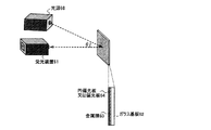
本実施例では、光源にメタルハライドランプ(シグマ工機製)IMH−250を用いて偏光板および波長板の組み合わせによる透過率の評価を行った。本実験のリファレンスは空気である。 In this example, a metal halide lamp (manufactured by Sigma Koki Co., Ltd.) IMH-250 was used as a light source, and the transmittance was evaluated by a combination of a polarizing plate and a wave plate. The reference for this experiment is air.
偏向板又は波長板((位相差板とも呼び、λ/4波長の位相差を与えるもの、λ/2波長の位相差を与えるものを使用)の配置条件は以下のとおりである。配置条件は光源からの順であり、()内は偏光板の吸収軸と波長板の遅相軸とのなす角度を示している。
(1)偏光板A+偏光板B
(2)偏光板A+λ/4波長板(45度)+λ/4波長板(45度)+偏光板B
(3)偏光板A+λ/2波長板(45度)+λ/2波長板(45度)+偏光板B
(4)偏光板A+λ/4波長板(80度)+λ/4波長板(80度)+λ/2板(17.5度)+偏光板B
条件(3)、(4)では波長板の位相の合計が1λとなっている。
Arrangement conditions of a deflector plate or a wave plate (also referred to as a phase difference plate, which gives a phase difference of λ / 4 wavelength, or a material which gives a phase difference of λ / 2 wavelength) are as follows. The order from the light source indicates the angle between the absorption axis of the polarizing plate and the slow axis of the wave plate.
(1) Polarizing plate A + polarizing plate B
(2) Polarizing plate A + λ / 4 wavelength plate (45 degrees) + λ / 4 wavelength plate (45 degrees) + polarizing plate B
(3) Polarizing plate A + λ / 2 wavelength plate (45 degrees) + λ / 2 wavelength plate (45 degrees) + polarizing plate B
(4) Polarizing plate A + λ / 4 wavelength plate (80 degrees) + λ / 4 wavelength plate (80 degrees) + λ / 2 plate (17.5 degrees) + polarizing plate B
In the conditions (3) and (4), the total phase of the wave plate is 1λ.
図5(A)には、条件(2)の場合の測定系を示す。光源51と、透過率測定器BM5A(受光装置)52との間に、λ/4板の遅相軸が、偏光板の吸収軸に対して45度をなすように(図5(B)参照)、偏光板(Pol)53、λ/4板54を配置している。 FIG. 5A shows a measurement system in the case of condition (2). Between the light source 51 and the transmittance measuring instrument BM5A (light receiving device) 52, the slow axis of the λ / 4 plate is 45 degrees with respect to the absorption axis of the polarizing plate (see FIG. 5B). ), A polarizing plate (Pol) 53, and a λ / 4 plate 54 are disposed.
表1に、配置条件(1)から(4)における透過光(cn/m)の最大値と最小値、及び規格値(最小値/最大値)の値を示す。()内は偏光板Bに対する偏光板Aの角度を示す。 Table 1 shows the maximum value and minimum value of transmitted light (cn / m) and the standard value (minimum value / maximum value) in the arrangement conditions (1) to (4). The values in parentheses indicate the angle of the polarizing plate A with respect to the polarizing plate B.

表1より、偏光板のみの組み合わせが漏れ光はもっとも小さく、黒レベルがよいことがわかる。また波長板の組み合わせでは条件(4)の黒レベルがもっとも良いが、偏光板のみと比べると黒レベルが低いことがわかる。また条件(3)のλ/2板の2枚使用は本実験においてもっとも黒レベルが悪かった。 From Table 1, it can be seen that the combination of the polarizing plates alone has the smallest leakage light and good black level. In addition, in the combination of the wave plates, the black level of the condition (4) is the best, but it can be seen that the black level is lower than that of the polarizing plate alone. The use of two λ / 2 plates under condition (3) had the worst black level in this experiment.
波長板を使用した場合、光漏れが発生し黒レベルが悪くなるのは、指定波長以外の波長成分が楕円偏光等になり、直線成分からズレた分が漏れ光となるためと考えられる(指定波長においても入射角度等により楕円成分が形成される)。条件(3)と条件(4)が透過光で見た場合のλ条件となる。条件(3)のλ/2板の連結構成では、より大きな位相差を制御する必要があるため前記楕円成分が大きくなり、漏れ光も増大してしまう。条件(4)のλ/2板、λ/4板の組み合わせでは、広帯域化条件を適用することにより上記の楕円偏光成分は条件(2)のλ/4板の連結構成時の半分、条件(3)の1/4程度に抑えられる。しかし、楕円成分は抑えきれず偏光板のみの場合と比較すると、黒が浮くこと結果となった。 When a wave plate is used, light leakage occurs and the black level deteriorates. Wavelength components other than the specified wavelength become elliptically polarized light, etc., and the amount of deviation from the linear component becomes leaked light (specified An elliptical component is also formed at the wavelength depending on the incident angle and the like). Condition (3) and condition (4) are λ conditions when viewed with transmitted light. In the connection configuration of the λ / 2 plates in the condition (3), it is necessary to control a larger phase difference, so that the elliptic component becomes large and leakage light also increases. In the combination of the λ / 2 plate and the λ / 4 plate in the condition (4), the above-mentioned elliptically polarized light component is half of the condition of the connection configuration of the λ / 4 plate in the condition (2) by applying the broadband condition. It is suppressed to about 1/4 of 3). However, the ellipse component could not be suppressed, resulting in the black floating compared to the case of the polarizing plate alone.
以上から、電極部での映り込み(反射成分)が少ない両面出射型表示装置の場合は、偏光板のみの組み合わせが黒レベルを沈め、コントラストを改善するために有効と考えられる。 From the above, in the case of a dual emission type display device with less reflection (reflection component) at the electrode part, it is considered that the combination of only the polarizing plates is effective for reducing the black level and improving the contrast.
両面出射型表示装置が実施の形態2に示すような構造を有する場合は、円偏光板を用いてもよいことは上述の通りである。 As described above, in the case where the dual emission type display device has a structure as shown in Embodiment Mode 2, a circularly polarizing plate may be used.
本実施例では、条件(1)のように配置した偏光板A、Bの角度依存性を測定した。本実験のリファレンスは空気である。以下に結果を示す。 In this example, the angle dependency of polarizing plates A and B arranged as in condition (1) was measured. The reference for this experiment is air. The results are shown below.
表2には、図5に示す測定系で偏光板A、Bのみを90度ずらしたクロスニコルに配置し、そこから偏光板Aの光軸の角度をずらしていったときの透過光と、ずれ角の結果を示す。また輝度は、クロスニコル状態を1として規格化している。偏光板の光軸は吸収軸とする。 In Table 2, in the measurement system shown in FIG. 5, only the polarizing plates A and B are arranged in crossed Nicols shifted by 90 degrees, and the transmitted light when the angle of the optical axis of the polarizing plate A is shifted therefrom, The result of the deviation angle is shown. The luminance is normalized with the crossed Nicols state set to 1. The optical axis of the polarizing plate is the absorption axis.
また表2に基づくグラフを図7に示す。 A graph based on Table 2 is shown in FIG.
以上の結果より、偏光板A、Bのずれ角は、輝度が5割程度低下する±45度以下、好ましくは輝度が3割程度低下する±30度以下、さらに好ましくは輝度が9.9割程度低下する±10度以下、さらに好ましくは±5度以下が許容範囲と考えられる。 From the above results, the deviation angle between the polarizing plates A and B is ± 45 degrees or less where the luminance is reduced by about 50%, preferably ± 30 degrees or less where the luminance is reduced by about 30%, more preferably 9.9%. A tolerance of ± 10 degrees or less, more preferably ± 5 degrees or less, is considered to be acceptable.
但し、本実験では光源にメタルハライドランプを使用しており、実際の発光素子を有するパネルを用いていない。そのため、発光素子の発光輝度が高ければ許容できるずれ角の許容範囲は大きくなり、コントラストが十分とれると考えられる。 However, in this experiment, a metal halide lamp is used as a light source, and a panel having an actual light emitting element is not used. For this reason, it is considered that if the light emission luminance of the light emitting element is high, the allowable range of the deviation angle is large, and sufficient contrast can be obtained.
本実施例では、光源にメタルハライドランプ(シグマ工機製)IMH−250を用いて偏光板、又は各種円偏光板を用いて反射光を測定する実験を行った。 In this example, an experiment was performed in which reflected light was measured using a polarizing plate or various circularly polarizing plates using a metal halide lamp (manufactured by Sigma Koki) IMH-250 as a light source.
まず、以下に示す条件で作製した試料を用意した。
(1)ガラス基板+金属膜
(2)ガラス基板+金属膜+偏光板
(3)ガラス基板+金属膜+λ/4波長板(45度)+偏光板
(4)ガラス基板+金属膜+λ/4波長板(80度)+λ/2波長板(17.5度)+偏光板
(5)ガラス基板+金属膜+λ/4波長板(45度)+λ/2波長板(45度)+偏光板
(6)ガラス基板+金属膜+λ/2波長板(45度)+偏光板
本実験のリファレンスは空気であり、金属膜はスパッタリング法によりAl−Ti膜を1000Å成膜した。
First, a sample prepared under the following conditions was prepared.
(1) Glass substrate + metal film (2) Glass substrate + metal film + polarizing plate (3) Glass substrate + metal film + λ / 4 wavelength plate (45 degrees) + polarizing plate (4) Glass substrate + metal film + λ / 4 Wavelength plate (80 degrees) + λ / 2 wavelength plate (17.5 degrees) + polarizing plate (5) glass substrate + metal film + λ / 4 wavelength plate (45 degrees) + λ / 2 wavelength plate (45 degrees) + polarizing plate ( 6) Glass substrate + metal film + λ / 2 wavelength plate (45 degrees) + polarizing plate The reference of this experiment was air, and the metal film was formed with 1000 μm of Al—Ti film by sputtering.
図6には、試料(3)の場合の測定系を示す。試料に対し、θ=30度をなすように光源61を入射し、反射光測定装置BM5A(受光装置)62を試料に対して垂直に配置し、反射光(cd/m)を測定した。 FIG. 6 shows a measurement system in the case of the sample (3). A light source 61 was incident on the sample so as to make θ = 30 degrees, a reflected light measuring device BM5A (light receiving device) 62 was arranged perpendicular to the sample, and reflected light (cd / m) was measured.
表3には、試料(1)〜(6)の実験結果を示す。 Table 3 shows the experimental results of samples (1) to (6).
表3からわかるように、反射光の防止効果が高いものは試料(3)、(4)、(5)である。 As can be seen from Table 3, samples (3), (4), and (5) have a high effect of preventing reflected light.
また試料(1)〜(6)に対して、自記分光光度計U4000(日立製作所製)により反射光を400〜80nmの範囲で測定した。その結果を図8に示す。 Moreover, with respect to the samples (1) to (6), reflected light was measured in the range of 400 to 80 nm with a self-recording spectrophotometer U4000 (manufactured by Hitachi, Ltd.). The result is shown in FIG.
図8からわかるように、低反射率を得られたものは試料(3)、(4)、(5)である。特に、試料(3)、(4)では、広い範囲において低反射率を得ることができ、好ましい。また、表3と比較すると、偏光板、又は波長板を設ける場合、かなり反射光を防止できることがわかる。 As can be seen from FIG. 8, samples (3), (4), and (5) obtained low reflectivity. In particular, samples (3) and (4) are preferable because low reflectance can be obtained in a wide range. Further, when compared with Table 3, it can be seen that when a polarizing plate or a wave plate is provided, the reflected light can be considerably prevented.
Claims (10)
第2の領域に配置された透光性を有する第2の電極と、
前記第1の電極上及び前記第2の電極上に設けられた発光層と、
前記発光層上に設けられた透光性を有する第3の電極と、
前記第3の電極上に設けられた非透光性材料を有する膜と、を一画素に有し、
前記第3の電極は、前記第1の領域及び前記第2の領域に配置されており、
前記非透光性材料を有する膜は、前記第2の領域に配置されており、
第1の偏光板及び第2の偏光板を有し、
前記第1の電極、前記第2の電極、前記第3の電極、前記発光層、及び前記非透光性材料を有する膜は、前記第1の偏光板と前記第2の偏光板との間に配置されていることを特徴とする表示装置。 A non-translucent first electrode disposed in the first region;
A second electrode having translucency disposed in the second region;
A light emitting layer provided on the first electrode and the second electrode;
A third electrode having translucency provided on the light emitting layer;
A film having a non-translucent material provided on the third electrode in one pixel;
The third electrode is disposed in the first region and the second region,
The film having the non-translucent material is disposed in the second region,
Having a first polarizing plate and a second polarizing plate;
The film including the first electrode, the second electrode, the third electrode, the light emitting layer, and the non-translucent material is between the first polarizing plate and the second polarizing plate. A display device characterized by being arranged in the above.
前記第1の偏光板の光軸と前記第2の偏光板の光軸とは、45度以上135度以下の角度をなすことを特徴とする表示装置。 In claim 1 ,
The display device, wherein an optical axis of the first polarizing plate and an optical axis of the second polarizing plate form an angle of 45 degrees or more and 135 degrees or less.
第2の領域に配置された透光性を有する第2の電極と、
前記第1の電極上及び前記第2の電極上に設けられた発光層と、
前記発光層上に設けられた透光性を有する第3の電極と、
前記第3の電極上に設けられた非透光性材料を有する膜と、を一画素に有し、
前記第3の電極は、前記第1の領域及び前記第2の領域に配置されており、
前記非透光性材料を有する膜は、前記第2の領域に配置されており、
第1の円偏光板及び第2の円偏光板を有し、
前記第1の電極、前記第2の電極、前記第3の電極、前記発光層、及び前記非透光性材料を有する膜は、前記第1の円偏光板と前記第2の円偏光板との間に配置されていることを特徴とする表示装置。 A non-translucent first electrode disposed in the first region;
A second electrode having translucency disposed in the second region;
A light emitting layer provided on the first electrode and the second electrode;
A third electrode having translucency provided on the light emitting layer;
A film having a non-translucent material provided on the third electrode in one pixel;
The third electrode is disposed in the first region and the second region,
The film having the non-translucent material is disposed in the second region,
Having a first circularly polarizing plate and a second circularly polarizing plate;
The first electrode, the second electrode, the third electrode, the light emitting layer, and the film having a non-translucent material are formed of the first circularly polarizing plate and the second circularly polarizing plate. A display device characterized by being arranged between.
前記第1の円偏光板は、第1の1/4λ波長板を有し、
前記第2の円偏光板は、第2の1/4λ波長板を有し、
前記第1の円偏光板が有する第1の偏光板の吸収軸と、前記第1の1/4λ波長板の遅相軸とは45度をなし、
前記第2の円偏光板が有する第2の偏光板の吸収軸と、前記第2の1/4λ波長板の遅相軸とは45度をなし、
前記第1の偏光板の吸収軸と前記第2の偏光板の吸収軸、及び、前記第1の1/4λ波長板の遅相軸と前記第2の1/4λ波長板の遅相軸は、それぞれ平行となることを特徴とする表示装置。 In claim 3 ,
The first circularly polarizing plate has a first quarter-wave plate.
The second circularly polarizing plate has a second ¼λ wavelength plate,
The absorption axis of the first polarizing plate of the first circularly polarizing plate and the slow axis of the first quarter-wave plate form 45 degrees,
The absorption axis of the second polarizing plate of the second circularly polarizing plate and the slow axis of the second ¼λ wavelength plate form 45 degrees,
The absorption axis of the first polarizing plate and the absorption axis of the second polarizing plate, and the slow axis of the first 1 / 4λ wavelength plate and the slow axis of the second 1 / 4λ wavelength plate are: A display device characterized by being parallel to each other.
前記第1の円偏光板は、第1の1/4λ波長板を有し、
前記第2の円偏光板は、第2の1/4λ波長板を有し、
前記第1の円偏光板が有する第1の偏光板の吸収軸と、前記第1の1/4λ波長板の遅相軸とは45度をなし、
前記第2の円偏光板が有する第2の偏光板の吸収軸と、前記第2の1/4λ波長板の遅相軸とは45度をなし、
前記第1の偏光板の吸収軸と前記第2の偏光板の吸収軸、及び、前記第1の1/4λ波長板の遅相軸と前記第2の1/4λ波長板の遅相軸は、それぞれ90度となることを特徴とする表示装置。 In claim 3 ,
The first circularly polarizing plate has a first quarter-wave plate.
The second circularly polarizing plate has a second ¼λ wavelength plate,
The absorption axis of the first polarizing plate of the first circularly polarizing plate and the slow axis of the first quarter-wave plate form 45 degrees,
The absorption axis of the second polarizing plate of the second circularly polarizing plate and the slow axis of the second ¼λ wavelength plate form 45 degrees,
The absorption axis of the first polarizing plate and the absorption axis of the second polarizing plate, and the slow axis of the first 1 / 4λ wavelength plate and the slow axis of the second 1 / 4λ wavelength plate are: , Each of which is 90 degrees.
前記第1の円偏光板は、第1の1/4λ波長板及び第1の1/2λ波長板を有し、
前記第2の円偏光板は、第2の1/4λ波長板及び第2の1/2λ波長板を有し、
前記第1の円偏光板が有する第1の偏光板の吸収軸と、前記第1の1/2λ波長板の遅相軸とは17.5度をなし、
前記第1の偏光板の吸収軸と、前記第1の1/4λ波長板の遅相軸とは80度をなし、
前記第2の円偏光板が有する第2の偏光板の吸収軸と、前記第2の1/2λ波長板の遅相軸とは17.5度をなし、
前記第2の偏光板の吸収軸と前記第2の1/4λ波長板の遅相軸とは80度をなし、
前記第1の偏光板の吸収軸と前記第2の偏光板の吸収軸、及び、前記第1の1/4λ波長板の遅相軸と前記第2の1/4λ波長板の遅相軸は、それぞれ平行となることを特徴とする表示装置。 In claim 3 ,
The first circularly polarizing plate has a first 1 / 4λ wavelength plate and a first 1 / 2λ wavelength plate,
The second circularly polarizing plate has a second 1 / 4λ wavelength plate and a second 1 / 2λ wavelength plate,
The absorption axis of the first polarizing plate of the first circularly polarizing plate and the slow axis of the first ½λ wavelength plate form 17.5 degrees,
The absorption axis of the first polarizing plate and the slow axis of the first quarter-wave plate form 80 degrees,
The absorption axis of the second polarizing plate of the second circularly polarizing plate and the slow axis of the second ½λ wavelength plate form 17.5 degrees,
The absorption axis of the second polarizing plate and the slow axis of the second quarter-wave plate form 80 degrees,
The absorption axis of the first polarizing plate and the absorption axis of the second polarizing plate, and the slow axis of the first 1 / 4λ wavelength plate and the slow axis of the second 1 / 4λ wavelength plate are: A display device characterized by being parallel to each other.
前記一画素に、第1のトランジスタ及び第2のトランジスタを有し、
前記第1の電極は、前記第1のトランジスタと電気的に接続されており、
前記第2の電極は、前記第2のトランジスタと電気的に接続されていることを特徴とする表示装置。 In any one of Claims 1 thru | or 6 ,
The one pixel has a first transistor and a second transistor,
The first electrode is electrically connected to the first transistor;
The display device, wherein the second electrode is electrically connected to the second transistor.
前記第1のトランジスタ上及び前記第2のトランジスタ上に設けられた絶縁膜を有し、
前記第1の電極及び前記第2の電極は、前記絶縁膜上に設けられていることを特徴とする表示装置。 In claim 7 ,
An insulating film provided on the first transistor and the second transistor;
The display device, wherein the first electrode and the second electrode are provided on the insulating film.
前記一画素に、トランジスタを有し、
前記第1の電極及び前記第2の電極は、前記トランジスタと電気的に接続されていることを特徴とする表示装置。 In any one of Claims 1 thru | or 6 ,
The one pixel has a transistor,
The display device, wherein the first electrode and the second electrode are electrically connected to the transistor.
前記トランジスタ上に設けられた絶縁膜を有し、
前記第1の電極及び前記第2の電極は、前記絶縁膜上に設けられていることを特徴とする表示装置。
In claim 9 ,
An insulating film provided on the transistor;
The display device, wherein the first electrode and the second electrode are provided on the insulating film.
Priority Applications (1)
| Application Number | Priority Date | Filing Date | Title |
|---|---|---|---|
| JP2005065596A JP4749004B2 (en) | 2003-05-16 | 2005-03-09 | Display device |
Applications Claiming Priority (3)
| Application Number | Priority Date | Filing Date | Title |
|---|---|---|---|
| JP2003139546 | 2003-05-16 | ||
| JP2003139546 | 2003-05-16 | ||
| JP2005065596A JP4749004B2 (en) | 2003-05-16 | 2005-03-09 | Display device |
Related Parent Applications (1)
| Application Number | Title | Priority Date | Filing Date |
|---|---|---|---|
| JP2003188990A Division JP4131838B2 (en) | 2003-05-16 | 2003-06-30 | Display device |
Related Child Applications (1)
| Application Number | Title | Priority Date | Filing Date |
|---|---|---|---|
| JP2009115296A Division JP5178625B2 (en) | 2003-05-16 | 2009-05-12 | E-book |
Publications (3)
| Publication Number | Publication Date |
|---|---|
| JP2005242370A JP2005242370A (en) | 2005-09-08 |
| JP2005242370A5 JP2005242370A5 (en) | 2006-07-27 |
| JP4749004B2 true JP4749004B2 (en) | 2011-08-17 |
Family
ID=35024088
Family Applications (1)
| Application Number | Title | Priority Date | Filing Date |
|---|---|---|---|
| JP2005065596A Expired - Fee Related JP4749004B2 (en) | 2003-05-16 | 2005-03-09 | Display device |
Country Status (1)
| Country | Link |
|---|---|
| JP (1) | JP4749004B2 (en) |
Families Citing this family (6)
| Publication number | Priority date | Publication date | Assignee | Title |
|---|---|---|---|---|
| US8217572B2 (en) * | 2005-10-18 | 2012-07-10 | Semiconductor Energy Laboratory Co., Ltd. | Display device with prism layer |
| EP1816508A1 (en) | 2006-02-02 | 2007-08-08 | Semiconductor Energy Laboratory Co., Ltd. | Display device |
| JP4968471B2 (en) * | 2007-10-11 | 2012-07-04 | 大日本印刷株式会社 | Light-emitting organic EL display panel |
| US8502211B2 (en) | 2010-06-30 | 2013-08-06 | Samsung Display Co., Ltd. | Organic light emitting diode display and manufacturing method thereof |
| CN114551427A (en) * | 2016-05-20 | 2022-05-27 | 群创光电股份有限公司 | Display device |
| CN112186024B (en) * | 2020-09-30 | 2022-11-08 | 天马微电子股份有限公司 | Display panel and display device |
Family Cites Families (6)
| Publication number | Priority date | Publication date | Assignee | Title |
|---|---|---|---|---|
| JP2002040428A (en) * | 1999-09-28 | 2002-02-06 | Stanley Electric Co Ltd | Liquid crystal display |
| US6801185B2 (en) * | 2000-04-14 | 2004-10-05 | C-360, Inc. | Illuminated viewing assembly, viewing system including the illuminated viewing assembly, and method of viewing therefor |
| JP4217426B2 (en) * | 2002-05-28 | 2009-02-04 | シャープ株式会社 | Double-sided display device |
| JP4234376B2 (en) * | 2002-08-28 | 2009-03-04 | 東芝松下ディスプレイテクノロジー株式会社 | Display device and electronic device |
| JP2004095340A (en) * | 2002-08-30 | 2004-03-25 | Seiko Instruments Inc | Self-luminous display device |
| JP2004205702A (en) * | 2002-12-24 | 2004-07-22 | Toshiba Matsushita Display Technology Co Ltd | Display device and mobile equipment |
-
2005
- 2005-03-09 JP JP2005065596A patent/JP4749004B2/en not_active Expired - Fee Related
Also Published As
| Publication number | Publication date |
|---|---|
| JP2005242370A (en) | 2005-09-08 |
Similar Documents
| Publication | Publication Date | Title |
|---|---|---|
| JP4131838B2 (en) | Display device | |
| KR101407586B1 (en) | Display device and operating method thereof | |
| JP4485184B2 (en) | LIGHT EMITTING DEVICE AND ELECTRONIC DEVICE | |
| US9448437B2 (en) | Display apparatus for controlling optical transmissivity | |
| TWI425280B (en) | Display device | |
| EP2618378B1 (en) | Organic light emitting display device | |
| KR100995067B1 (en) | Organic light emitting display | |
| US9436053B2 (en) | Display unit and electronic apparatus | |
| US9391127B2 (en) | Display device for controlling light transmittance | |
| KR20110084771A (en) | Organic light emitting display | |
| TWI439171B (en) | Display device | |
| TWI425460B (en) | Display device | |
| JP5178625B2 (en) | E-book | |
| JP4749004B2 (en) | Display device | |
| KR20040042249A (en) | Organic electro luminesence display device with liquid crystal display portion | |
| JP4515398B2 (en) | Display device | |
| JP2007180024A (en) | Display |
Legal Events
| Date | Code | Title | Description |
|---|---|---|---|
| A521 | Request for written amendment filed |
Free format text: JAPANESE INTERMEDIATE CODE: A523 Effective date: 20060608 |
|
| A621 | Written request for application examination |
Free format text: JAPANESE INTERMEDIATE CODE: A621 Effective date: 20060608 |
|
| A131 | Notification of reasons for refusal |
Free format text: JAPANESE INTERMEDIATE CODE: A131 Effective date: 20090421 |
|
| A521 | Request for written amendment filed |
Free format text: JAPANESE INTERMEDIATE CODE: A523 Effective date: 20090514 |
|
| A131 | Notification of reasons for refusal |
Free format text: JAPANESE INTERMEDIATE CODE: A131 Effective date: 20100615 |
|
| A521 | Request for written amendment filed |
Free format text: JAPANESE INTERMEDIATE CODE: A523 Effective date: 20100625 |
|
| A01 | Written decision to grant a patent or to grant a registration (utility model) |
Free format text: JAPANESE INTERMEDIATE CODE: A01 Effective date: 20110510 |
|
| A01 | Written decision to grant a patent or to grant a registration (utility model) |
Free format text: JAPANESE INTERMEDIATE CODE: A01 |
|
| A61 | First payment of annual fees (during grant procedure) |
Free format text: JAPANESE INTERMEDIATE CODE: A61 Effective date: 20110517 |
|
| R150 | Certificate of patent or registration of utility model |
Free format text: JAPANESE INTERMEDIATE CODE: R150 |
|
| FPAY | Renewal fee payment (event date is renewal date of database) |
Free format text: PAYMENT UNTIL: 20140527 Year of fee payment: 3 |
|
| FPAY | Renewal fee payment (event date is renewal date of database) |
Free format text: PAYMENT UNTIL: 20140527 Year of fee payment: 3 |
|
| R250 | Receipt of annual fees |
Free format text: JAPANESE INTERMEDIATE CODE: R250 |
|
| R250 | Receipt of annual fees |
Free format text: JAPANESE INTERMEDIATE CODE: R250 |
|
| R250 | Receipt of annual fees |
Free format text: JAPANESE INTERMEDIATE CODE: R250 |
|
| R250 | Receipt of annual fees |
Free format text: JAPANESE INTERMEDIATE CODE: R250 |
|
| LAPS | Cancellation because of no payment of annual fees |