JP4654509B2 - Power supply voltage conversion circuit, control method therefor, display device and portable terminal - Google Patents
Power supply voltage conversion circuit, control method therefor, display device and portable terminal Download PDFInfo
- Publication number
- JP4654509B2 JP4654509B2 JP2000372352A JP2000372352A JP4654509B2 JP 4654509 B2 JP4654509 B2 JP 4654509B2 JP 2000372352 A JP2000372352 A JP 2000372352A JP 2000372352 A JP2000372352 A JP 2000372352A JP 4654509 B2 JP4654509 B2 JP 4654509B2
- Authority
- JP
- Japan
- Prior art keywords
- circuit
- power supply
- pulse
- clamping
- voltage
- Prior art date
- Legal status (The legal status is an assumption and is not a legal conclusion. Google has not performed a legal analysis and makes no representation as to the accuracy of the status listed.)
- Expired - Fee Related
Links
Images


Landscapes
- Liquid Crystal Display Device Control (AREA)
- Control Of Indicators Other Than Cathode Ray Tubes (AREA)
- Control Of El Displays (AREA)
- Dc-Dc Converters (AREA)
Description
【0001】
【発明の属する技術分野】
本発明は、電源電圧変換回路およびその制御方法、ならびに表示装置および携帯端末に関し、特にチャージポンプを用いた電源電圧変換回路およびその制御方法、ならびに当該電源電圧変換回路を搭載した表示装置およびこの表示装置を備えた携帯端末に関する。
【0002】
【従来の技術】
近年、携帯電話機やPDA(Personal Digital Assistants)などの携帯端末の普及がめざましい。これら携帯端末の急速な普及の要因の一つとして、その出力表示部として搭載されている液晶表示装置が挙げられる。その理由は、液晶表示装置が原理的に駆動するための電力を要しない特性を持ち、低消費電力の表示デバイスであるためである。
【0003】
携帯端末では、電源として単一電源電圧のバッテリが用いられる。一方、液晶表示装置において、マトリクス状に配された画素を駆動する水平駆動回路では、ロジック部とアナログ部とで異なる直流電圧が用いられ、また画素に情報を書き込む垂直駆動回路では、水平駆動回路側よりも絶対値の大きい直流電圧が用いられることになる。したがって、携帯端末に搭載される液晶表示装置には、単一の直流電圧を電圧値の異なる複数種類の直流電圧に変換する電源電圧変換回路、いわゆるDC−DCコンバータ(以下、DDコンバータと記す)が用いられる。
【0004】
従来、液晶表示装置におけるDDコンバータには、インダクタLを用いたものが一般的に使用されてきたが、近年の携帯端末の低消費電力化、小型化に伴ってチャージポンプ型のものも多く使用されるようになってきている。チャージポンプ型DDコンバータは、電流容量が比較的少ないものの、外付け部品としてインダクタLを使わなくて済むため携帯端末の小型化に寄与できるという利点を持っている。
【0005】
図11に、従来例1に係るチャージポンプ型DDコンバータの構成を示す。同図において、(A)は負電圧発生タイプを、(B)は昇圧タイプをそれぞれ示しており、基本的な構成は同じである。
【0006】
図11(A)において、単一の直流電圧VCCを与える電源とグランド(GND)との間には、PchMOSトランジスタQp101とNchMOSトランジスタQn101とが直列に接続され、かつ各ゲートが共通に接続されてCMOSインバータ101を構成している。このCMOSインバータ101のゲート共通接続点には、パルス発生源102から所定の周波数のスイッチングパルスが印加される。
【0007】
CMOSインバータ101のドレイン共通接続点(ノードA)には、コンデンサC101の一端が接続されている。コンデンサC101の他端には、ダイオードD101のアノードおよびダイオードD102のカソードがそれぞれ接続されている。ダイオードD101のカソードは接地されている。ダイオードD102のアノードとグランドとの間には負荷コンデンサC102が接続されている。
【0008】
上記構成の負電圧発生タイプのDDコンバータにおいては、原理的に、電源電圧VCCの−1倍、即ち負の直流電圧−VCCが負荷コンデンサC102の両端間に導出されることになる。一方、図11(B)に示す昇圧タイプのDDコンバータにおいては、ダイオードD101がコンデンサC101の他端と電源(VCC)との間に接続されている点が図11(A)の回路と相違するのみであり、原理的に、電源電圧VCCの2倍、即ち直流電圧2×VCCが負荷コンデンサC102の両端間に導出されることになる。
【0009】
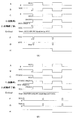
しかしながら、上記構成の従来例1に係るチャージポンプ型DDコンバータでは、ダイオードD101によるクランプを利用した構成であるため、図12のタイミングチャートから明らかなように、無負荷時でも出力電圧Voutが−1倍あるいは2倍の電圧値に到達せず、ダイオードのしきい値電圧Vthの2倍分だけシフトしてしまうという問題がある。なお、図12(A),(B)の各タイミングチャートには、図11(A),(B)の各回路におけるノードA〜Cの各信号波形A〜Cを示している。
【0010】
この従来例1の問題点を改善したのが、図13に示す従来例2に係るチャージポンプ型DDコンバータである。図13において、図11と同等部分には同一符号を付して示している。また、(A)は負電圧発生タイプを、(B)は昇圧タイプをそれぞれ示しており、基本的な構成は同じである。
【0011】
図13において、コンデンサC101の他端には、NchMOSトランジスタQn102のドレインおよびPchMOSトランジスタQp102のソースがそれぞれ接続されている。NchMOSトランジスタQn102のソースとグランドとの間には、負荷コンデンサC102が接続されている。PchMOSトランジスタQp102のドレインは接地されている。
【0012】
CMOSインバータ101のゲート共通接続点には、コンデンサC103の一端が接続されている。コンデンサC103の他端には、ダイオードD101のアノード、NchMOSトランジスタQn102およびPchMOSトランジスタQp102の各ゲートがそれぞれ接続されている。ダイオードD101のカソードは接地されている。
【0013】
上記構成の負電圧発生タイプのDDコンバータにおいては、図14(A)のタイミングチャートから明らかなように、無負荷時に出力電圧Voutが電源電圧VCCの−1倍の電圧値に到達することになる。一方、図13(B)に示す昇圧タイプのDDコンバータでは、スイッチングトランジスタQp103,Qn103が逆導電型となるとともに、ダイオードD101がコンデンサC101の他端と電源(VCC)との間に接続されている点が図13(A)の回路と相違するのみであり、無負荷時に出力電圧Voutが電源電圧VCCの2倍の電圧値に到達することになる。
【0014】
なお、図14(A),(B)の各タイミングチャートには、図13(A),(B)の各回路におけるノードA〜Cの各信号波形A〜Cを示している。
【0015】
【発明が解決しようとする課題】
しかしながら、上記構成の従来例2に係るチャージポンプ型DDコンバータでは、スイッチングトランジスタ(MOSトランジスタQn102,Qp102)に対するスイッチングパルス電圧、即ちノードDの電圧レベルがダイオードD101のしきい値電圧Vthだけシフトした電圧値でクランプされるため、スイッチングトランジスタ、特にPchMOSトランジスタQp102に対して十分な駆動電圧をとれない場合が起こる。
【0016】
このため、PchMOSトランジスタQp102のトランジスタサイズを大きく設定しなければならなく、その結果、トランジスタサイズの増加によって回路面積が増加したり、あるいは電流容量が低下するなどの問題が発生する。また、省電力モード等においてポンピング動作を一時的に止めた場合に、スイッチングパルスのデューティ比の変化とともに、スイッチングパルス電圧のクランプレベルが変動してしまい、結果として、電流容量の低下などの問題が発生する。
【0017】
上記の問題は、いずれもトランジスタのしきい値Vthが大きなとき、また、そのばらつきが大きなときに深刻となる。たとえば、薄膜トランジスタ(TFT;Thin Film Transistor)を用いてガラス基板上に回路を形成する場合にその問題は重要なポイントとなる。なお、薄膜トランジスタの形成に使用されるアモルファスシリコンやポリシリコン(多結晶シリコン)は、単結晶シリコンに比べて結晶性が悪く、導電機構の制御性が悪いことから、形成された薄膜トランジスタは、その特性のばらつきが大きいことが知られている。
【0018】
本発明は、上記課題に鑑みてなされたものであり、その目的とするところは、小面積の回路規模にて大きな電流容量を得ることが可能な電源電圧変換回路およびその制御方法、ならびに当該電源電圧変換回路を搭載した表示装置およびこの表示装置を備えた携帯端末を提供することにある。
【0019】
【課題を解決するための手段】
上記目的を達成するために、本発明では、出力部にスイッチ素子を有するチャージポンプを用いた電源電圧変換回路において、前記スイッチ素子に対する制御パルス電圧を起動時にダイオードクランプする第1のクランプ回路と、前記制御パルス電圧を起動プロセス終了時に回路電源電位にクランプする第2のクランプ回路とを設けたことを特徴としている。そして、この電源電圧変換回路は、表示装置の電源回路として用いられる。また、この電源電圧変換回路を備えた表示装置は、携帯端末の表示部として用いられる。
【0020】
上記構成の電源電圧変換回路において、起動時(電源投入時)に第1のクランプ回路がダイオードクランプすることで、制御パルス電圧の電圧値が回路電源電位からダイオードのしきい値電圧分だけシフトした電位にクランプされる。この制御パルスに基づいて出力部のスイッチ素子が動作することで、出力電圧が導出される。そして、起動プロセス終了時には、制御パルス電圧の電圧値が回路電源電位にクランプされる。これにより、以降のポンピング動作において、スイッチ素子に対して十分な駆動電圧が得られる。
【0021】
【発明の実施の形態】
以下、本発明の実施の形態について図面を参照して詳細に説明する。図1は、本発明の一実施形態に係る電源電圧変換回路であるチャージポンプ型DDコンバータの構成例を示す回路図であり、(A)は負電圧発生タイプを、(B)は昇圧タイプをそれぞれ示している。
【0022】
図1において、単一の直流電源電圧VCCを与える電源とグランド(GND)との間には、PchMOSトランジスタQp11とNchMOSトランジスタQn11とが直列に接続され、かつ各ゲートが共通に接続されてCMOSインバータ11を構成している。このCMOSインバータ11のゲート共通接続点には、パルス発生源12から所定の周波数のスイッチングパルスが印加される。
【0023】
CMOSインバータ11のドレイン共通接続点(ノードB)には、コンデンサC11の一端が接続されている。コンデンサC11の他端には、スイッチ素子、例えばNchMOSトランジスタQn12のドレインおよびPMOSトランジスタQp12のソースがそれぞれ接続されている。NchMOSトランジスタQn12のソースとグランドとの間には、負荷コンデンサC12が接続されている。
【0024】
CMOSインバータ11のゲート共通接続点には、コンデンサC13の一端が接続されている。コンデンサC13の他端には、ダイオードD11のアノードが接続されている。ダイオードD11は、そのカソードが接地されて第1のクランプ回路13を構成している。コンデンサC13の他端にはさらに、NchMOSトランジスタQn12およびPchMOSトランジスタQp12の各ゲートがそれぞれ接続されている。PchMOSトランジスタQp12のドレインは接地されている。
【0025】
コンデンサC13の他端とグランドとの間には、PchMOSトランジスタQp13が接続されている。このPchMOSトランジスタQp13のゲートには、パルス発生源14で発生されるクランプ用パルスがレベルシフト回路15でレベルシフトされて与えられる。これらPchMOSトランジスタQp13、パルス発生源14およびレベルシフト回路15は、スイッチングトランジスタ(NchMOSトランジスタQn12およびPchMOSトランジスタQp12)のスイッチングパルス電圧をクランプする第2のクランプ回路16を構成している。
【0026】
この第2のクランプ回路16において、レベルシフト回路15は、本DDコンバータに入力される電源電圧VCCを正側回路電源、負荷コンデンサC12の両端から導出される本回路の出力電圧Voutを負側回路電源とし、パルス発生源14で発生される第1の振幅(VCC−0[V])のクランプ用パルスを、第2の振幅(VCC−Vout[V])のクランプ用パルスにレベルシフトしてPchMOSトランジスタQp13のゲートに与える。これにより、PchMOSトランジスタQp13のスイッチング動作がより確実に行われることになる。
【0027】
次に、上記構成の負電圧発生タイプのチャージポンプ型DDコンバータにおける回路動作につき、図2(A)のタイミングチャートを用いて説明する。なお、図2(A)のタイミングチャートには、図1(A)の回路におけるノードA〜Gの各信号波形A〜Gを示している。
【0028】
電源投入時(起動時)には、パルス発生源12で発生されるスイッチングパルスに基づくコンデンサC13の出力電位、即ちノードDの電位は、先ずダイオードD11によって、負側の回路電源電位であるグランド(GND)レベルからダイオードD11のしきい値電圧Vth分だけレベルシフトした電位に“H”レベルクランプされる。
【0029】
そして、スイッチングパルスが“L”レベル(0V)のときは、PchMOSトランジスタQp11,Qp12がオン状態となるため、コンデンサC11が充電される。このとき、NchMOSトランジスタQn11がオフ状態にあるため、ノードBの電位がVCCレベルとなる。次いで、スイッチングパルスが“H”レベル(VCC)になると、NchMOSトランジスタQn11,Qn12がオン状態となり、ノードBの電位がグランドレベル(0V)になるため、ノードCの電位が−VCCレベルとなる。このノードCの電位がそのままNchMOSトランジスタQn12を通して出力電圧Vout(=−VCC)となる。
【0030】
次に、出力電圧Voutがある程度立ち上がると(起動プロセス終了時)、クランプパルス用のレベルシフト回路15が動作を始める。このレベルシフト回路15が動作し始めると、パルス発生源14で発生された振幅VCC−0[V]のクランプ用パルスは、当該レベルシフト回路15において、振幅VCC−Vout[V]のクランプ用パルスにレベルシフトされ、しかる後PchMOSトランジスタQp13のゲートに印加される。
【0031】
このとき、クランプ用パルスの“L”レベルが出力電圧Vout、即ち−VCCであるため、PchMOSトランジスタQp13が確実にオン状態となる。これにより、ノードDの電位は、グランドレベルからダイオードD11のしきい値電圧Vth分だけレベルシフトした電位ではなく、グランドレベル(負側の回路電源電位)にクランプされる。これにより、以降のポンピング動作において、特にPchMOSトランジスタQp12に対して十分な駆動電圧が得られる。
【0032】
上述したように、チャージポンプを用いたDDコンバータにおいて、その出力部に設けられたスイッチ素子(NchMOSトランジスタQn12およびPchMOSトランジスタQp12)に対する制御パルス(スイッチングパルス)電圧を、本回路の起動時には先ず第1のクランプ回路13のダイオードD11によるクランプ、起動プロセス終了後は第2のクランプ回路16によるクランプ、というように2段階に分けてクランプすることにより、特にPchMOSトランジスタQp12に対して十分な駆動電圧をとることができる。
【0033】
これにより、PchMOSトランジスタQp12において十分なスイッチング電流が得られるようになるため、安定したDC−DC変換動作が行えるようになるとともに、変換効率を向上させることができる。特に、PchMOSトランジスタQp12のトランジスタサイズを大きくしなくても、十分なスイッチング電流が得られるため、小面積の回路規模にて電流容量の大きなDDコンバータを実現できる。その効果は、しきい値Vthが大きいトランジスタ、例えば薄膜トランジスタを用いた場合に特に大きい。
【0034】
図1(B)に示す昇圧タイプのDDコンバータにおいても、基本的な回路構成および回路動作は同じである。
【0035】
すなわち、図1(B)において、スイッチングトランジスタおよび第2のクランプ用トランジスタ(MOSトランジスタQp14,Qn14,Qn13)が、図1(A)の回路のMOSトランジスタQn12,Qp12,Qp13と逆導電型となるとともに、ダイオードD11がコンデンサC11の他端と電源(VCC)との間に接続され、かつレベルシフト回路15が本回路の出力電圧Voutを正側回路電源とし、グランドレベルを負側回路電源とした構成となっており、この点が図1(A)の回路と構成上相違するのみである。
【0036】
回路動作上においても、基本的には、図1(A)の回路と全く同じである。異なるのは、スイッチングパルス電圧(制御パルス電圧)が起動時に先ずダイオードクランプされ、起動プロセス終了時にVCCレベル(正側の回路電源電位)にクランプされ、また出力電圧Voutとして電源電圧VCCの2倍の電圧値2×VCCが導出される点だけである。図2(B)に、図1(B)の回路におけるノードA〜Gの各信号波形A〜Gのタイミングチャートを示す。
【0037】
[適用例]
上記実施形態に係るチャージポンプ型のDDコンバータ(電源電圧変換回路)は、例えば、電気光学素子として液晶セルを用いた画素がマトリクス状に配置されてなるアクティブマトリクス型液晶表示装置などの表示装置の電源回路として用いられる。その構成の一例を図3に示す。ここでは、液晶表示装置の場合を例に採って説明するものとする。
【0038】
図3において、透明絶縁基板、例えばガラス基板21上には、液晶セルを含む画素がマトリクス状に多数配置されてなる表示エリア部22と共に、上下一対のHドライバ(水平駆動回路)23U,23DおよびVドライバ(垂直駆動回路)24が搭載され、さらに先述した実施形態に係るチャージポンプ型電源電圧変換回路25が搭載されている。ガラス基板21は、能動素子(例えば、トランジスタ)を含む多数の画素回路がマトリクス状に配置形成される第1の基板と、この第1の基板と所定の間隙をもって対向して配置される第2の基板とによって構成される。そして、これら第1,第2の基板間に液晶が封止される。
【0039】
図4に、表示エリア部22の具体的な構成の一例を示す。ここでは、図面の簡略化のために、3行(n−1行〜n+1行)4列(m−2列〜m+1列)の画素配列の場合を例に採って示している。図4において、表示エリア部22には、垂直走査ライン…,26n−1,26n,26n+1,…と、データライン…,27m−2,27m−1,27m,27m+1,…とがマトリクス状に配線され、それらの交点部分に単位画素28が配置されている。
【0040】
単位画素28は、画素トランジスタである薄膜トランジスタTFT、液晶セルLCおよび保持容量Csを有する構成となっている。ここで、液晶セルLCは、薄膜トランジスタTFTで形成される画素電極(一方の電極)とこれに対向して形成される対向電極(他方の電極)との間で発生する容量を意味する。
【0041】
薄膜トランジスタTFTは、ゲート電極が垂直走査ライン…,26n−1,26n,26n+1,…に接続され、ソース電極がデータライン…,27m−2,27m−1,27m,27m+1,…に接続されている。液晶セルLCは、画素電極が薄膜トランジスタTFTのドレイン電極に接続され、対向電極が共通ライン29に接続されている。保持容量Csは、薄膜トランジスタTFTのドレイン電極と共通ライン29との間に接続されている。共通ライン29には、所定の直流電圧がコモン電圧Vcomとして与えられる。
【0042】
垂直走査ライン…,26n−1,26n,26n+1,…の各一端は、図3に示すVドライバ24の対応する行の各出力端にそれぞれ接続される。Vドライバ24は、例えばシフトレジスタによって構成され、垂直転送クロックVCK(図示せず)に同期して順次垂直選択パルスを発生して垂直走査ライン…,26n−1,26n,26n+1,…に与えることによって垂直走査を行う。
【0043】
一方、表示エリア部22において、例えば、奇数番目のデータライン…,27m−1,27m+1,…の各一端が図3に示すHドライバ23Uの対応する列の各出力端に、偶数番目のデータライン…,27m−2,27m,…の各他端が図3に示すHドライバ23Dの対応する列の各出力端にそれぞれ接続される。Hドライバ23U,23Dの具体的な構成の一例を図5に示す。
【0044】
図5に示すように、Hドライバ23Uは、シフトレジスタ31U、サンプリングラッチ回路(データ信号入力回路)32U、線順次化ラッチ回路33UおよびDA変換回路34Uを有する構成となっている。シフトレジスタ31Uは、水平転送クロックHCK(図示せず)に同期して各転送段から順次シフトパルスを出力することによって水平走査を行う。サンプリングラッチ回路32Uは、シフトレジスタ31Uから与えられるシフトパルスに応答して、入力される所定ビットのディジタル画像データを点順次にてサンプリングしてラッチする。
【0045】
線順次化ラッチ回路33Uは、サンプリングラッチ回路32Uで点順次にてラッチされたディジタル画像データを1ライン単位で再度ラッチすることによって線順次化し、この1ライン分のディジタル画像データを一斉に出力する。DA変換回路34Uは例えば基準電圧選択型の回路構成をとり、線順次化ラッチ回路33Uから出力される1ライン分のディジタル画像データをアナログ画像信号に変換して先述した画素エリア部22のデータライン…,27m−2,27m−1,27m,27m+1,…に与える。
【0046】
下側のHドライバ23Dについても、上側のHドライバ23Uと全く同様に、シフトレジスタ31D、サンプリングラッチ回路32D、線順次化ラッチ回路33DおよびDA変換回路34Dを有する構成となっている。なお、本例に係る液晶表示装置では、表示エリア部22の上下にHドライバ23U,23Dを配する構成を採ったが、これに限定されるものではなく、上下のいずれか一方のみに配する構成を採ることも可能である。
【0047】
図3および図5から明らかなように、先述した実施形態に係るチャージポンプ型電源電圧変換回路25についても、表示エリア部22と同一のガラス基板21上に集積される。ここで、例えば表示エリア部22の上下にHドライバ23U,23Dを配する構成を採る液晶表示装置の場合には、Hドライバ23U,23Dが搭載されていない辺の額縁エリア(表示エリア部22の周辺エリア)に電源電圧変換回路25を搭載するのが好ましい。
【0048】
何故ならば、Hドライバ23U,23Dは、上述した如くVドライバ24に比べて構成要素が多く、その回路面積が非常に大きくなる場合が多いことから、Hドライバ23U,23Dが搭載されていない辺の額縁エリアに搭載することで、有効画面率(ガラス基板21に対する有効エリア部22の面積率)を低下させることなく、電源電圧変換回路25を表示エリア部22と同一のガラス基板21上に集積することができるからである。
【0049】
なお、本例に係る液晶表示装置においては、Hドライバ23U,23Dが搭載されていない辺の額縁エリアの一方側にはVドライバ24が集積されていることから、その反対側の辺の額縁エリアに電源電圧変換回路25を集積する構成を採っている。
【0050】
また、電源電圧変換回路25の集積に際しては、表示エリア部22の各画素トランジスタとして薄膜トランジスタTFTを用いていることから、電源電圧変換回路25を構成するトランジスタ、即ち図1におけるMOSトランジスタQp11〜Qp13,Qn11〜Qn13やレベルシフト回路15を構成するトランジスタなどとしても薄膜トランジスタを用い、少なくともこれらトランジスタ回路を表示エリア部22と同一プロセスを用いて作成することにより、その製造が容易となるとともに、低コストにて実現できる。
【0051】
特に、トランジスタ回路のうち、CMOSトランジスタ11については0V−VCCで動作することから、これを除いた高耐圧の必要なダイオードD11、MOSトランジスタQp12,Qp13,Qn12,Qn13、レベルシフト回路15を構成するトランジスタについては、薄膜トランジスタで作成すると素子分離が不要なため、表示エリア部22と同一プロセスを用いて作成することで、その作成が容易になる。この場合、他のトランジスタ回路などについては、ガラス基板21とは別の基板上にシリコンチップで作成するようにすれば良い。
【0052】
なお、上記の適用例では、先述した実施形態に係るチャージポンプ型電源電圧変換回路をガラス基板21上に表示エリア部22と一体的に形成するとしたが、必ずしも表示エリア部22と一体形成する必要はなく、液晶表示装置の外部回路として用いても良く、またガラス基板21とは別の基板上に作成するようにしても良い。
【0053】
ただし、表示エリア部22と同一の基板上に一体形成した方が有利であることは、上述したことから明らかである。しかも、先述した実施形態に係るチャージポンプ型電源電圧変換回路は、小面積の回路規模にて大きな電流容量を得ることができ、また特に薄膜トランジスタのように、しきい値Vthが大きいトランジスタを用いた場合にその効果が極めて大であるため、当該電源電圧変換回路を表示エリア部22と同一の基板上に一体形成することで、液晶表示装置を含むセットの低コスト化、さらには薄型化、コンパクト化に大きく寄与できる。
【0054】
ところで、液晶表示装置には、装置全体の低消費電力化を図るために、省電力モードを選択的に採る構成のものがある。具体的には、図6に示すように、外部からのモードの指定情報に基づいて、電源電圧変換回路25に対して省電力モードの制御を行うための省電力モードコントロール回路35が設けられる。なお、図6においては、Hドライバ23U,23DおよびVドライバ24を一つのブロック(ドライバ部)で一括して示している。
【0055】
[応用例1]
図7は、先述した実施形態に係るチャージポンプ型電源電圧変換回路、即ちDDコンバータ(図1を参照)の応用例1を示す回路図であり、省電力モードを選択的に採る液晶表示装置に用いる場合を示している。図7において、(A)は負電圧発生タイプを、(B)は昇圧タイプをそれぞれ示しており、図中、図1と同等部分には同一符号を付して示している。
【0056】
図7(A),(B)において、CMOSインバータ11の前段に2入力AND回路17が新たに付加された以外は、図1の構成と全く同じである。2入力AND回路17は、パルス発生源12で発生されるスイッチングパルスを一方の入力とし、図6に示す省電力モードコントロール回路35から省電力モード時に供給される“L”レベルのモード選択信号SELを他方の入力としている。
【0057】
上記構成の応用例1に係るDDコンバータでは、省電力モード時に“L”レベルのモード選択信号SELが供給されることで、AND回路17はパルス発生源12で発生されるスイッチングパルスのDDコンバータ内回路への供給を停止する。これにより、チャージポンプのポンピング動作が一時的に停止するため、DDコンバータ内回路での消費電流が低下し、省電力化が図られる。
【0058】
また、省電力モードの設定によってチャージポンプのクロック供給が一時的に停止するような場合でも、先述したように、出力部に設けられたスイッチ素子(NchMOSトランジスタQn12およびPchMOSトランジスタQp12)に対する制御パルス(スイッチングパルス)の電圧を、起動時と起動プロセス終了後で2段階に分けてクランプするようにしたことにより、ノードDのクランプレベルが安定となるため、クロック供給/停止の移行期間においても十分な電流能力を確保でき、よって安定したDC−DC変換動作が可能になる。
【0059】
[応用例2]
図8は、先述した実施形態に係るチャージポンプ型電源電圧変換回路、即ちDDコンバータ(図1を参照)の応用例2を示す回路図であり、出力電位のレギュレーション機能を有するDDコンバータとして用いる場合を示している。図8において、(A)は負電圧発生タイプを、(B)は昇圧タイプをそれぞれ示しており、図中、図1と同等部分には同一符号を付して示している。
【0060】
図8(A),(B)において、本例に係るレギュレーション回路は、回路出力端(ノードE)と電源(VCC)またはグランドとの間に直列接続された抵抗R1,R2と、これら抵抗R1,R2の分圧点に非反転(+)入力端が接続され、反転(−)入力端に基準電圧(本例では、グランドレベル)が与えられるコンパレータ18と、CMOSインバータ11の前段に配置され、パルス発生源12で発生されるスイッチングパルスを一方の入力とし、コンパレータ18の比較出力を他方の入力とするAND回路19とを有する構成となっている。
【0061】
このレギュレーション回路が新たに付加された以外は、図1の構成と全く同じであり、またチャージポンプ動作についても基本的に図1の回路と同じである。図9(A),(B)に、図8(A),(B)の回路動作を説明するためのタイミングチャートを示す。なお、図9(A),(B)のタイミングチャートには、図8(A),(B)の各回路におけるノードA〜Hの各信号波形A〜Hをそれぞれ示している。
【0062】
上記構成の応用例2に係るDDコンバータでは、出力電圧Voutをコンパレータ18において基準電圧(例えば、負電圧発生タイプ(A)のときグランドレベル、昇圧タイプ(B)のとき基準電圧Vref)と比較し、その比較結果に基づいてAND回路18においてスイッチングパルスの供給/停止を制御することにより、出力電圧Voutが例えばグランドレベル(0V)になるようにレギュレーションする回路動作が行われる。
【0063】
負電圧発生タイプ(A)の場合には、出力電圧Voutが目標の電圧よりも下がったときにスイッチングパルスの供給を停止するようにフィードバックがかかり、結果として、抵抗R1,R2の分圧比で決まる目的の電圧値が出力電圧Voutとして得られる。昇圧タイプ(B)の場合は、出力電圧Voutが目標の電圧よりも上がったときにスイッチングパルスの供給を停止するようにフィードバックがかかり、結果として、抵抗R1,R2の分圧比で決まる目的の電圧値が出力電圧Voutとして得られる。
【0064】
また、レギュレーション動作によってチャージポンプのクロック供給が一時的に停止するような場合であっても、先述したように、スイッチ素子(NchMOSトランジスタQn12およびPchMOSトランジスタQp12)に対する制御パルス(スイッチングパルス)の電圧を、起動時と起動プロセス終了後で2段階に分けてクランプするようにしたことにより、ノードDのクランプレベルが安定するため、安定したレギュレーション動作が可能になる。
【0065】
以上説明した応用例1,2に係るDDコンバータ(電源電圧変換回路)についても、先述した実施形態に係るDDコンバータ(図1を参照)と同様に、図5に示したアクティブマトリクス型液晶表示装置の電源回路として用いることができる。また、本発明は、液晶表示装置への適用に限らず、エレクトロルミネッセンス(EL)素子を各画素の電気光学素子として用いたEL表示装置などの他のアクティブマトリクス型表示装置にも同様に適用可能である。
【0066】
また、本発明に係る表示装置は、パーソナルコンピュータ、ワードプロセッサ等のOA機器やテレビジョン受像機などのディスプレイとして用いられる外、特に装置本体の小型化、コンパクト化が進められている携帯電話機やPDAなどの携帯端末の表示部として用いて好適なものである。
【0067】
図10は、本発明が適用される携帯端末、例えば携帯電話機の構成の概略を示す外観図である。
【0068】
本例に係る携帯電話機は、装置筐体41の前面側に、スピーカ部42、表示部43、操作部44およびマイク部45が上部側から順に配置された構成となっている。かかる構成の携帯電話機において、表示部43には例えば液晶表示装置が用いられ、この液晶表示装置として、先述した実施形態あるいはその応用例1,2に係る電源電圧変換回路(DDコンバータ)を搭載した液晶表示装置が用いられる。
【0069】
このように、携帯電話機などの携帯端末において、先述した実施形態あるいはその応用例1,2に係る電源電圧変換回路を搭載した液晶表示装置を表示部43として用いることにより、これら電源電圧変換回路が小面積の回路規模にて大きな電流容量を得ることが可能であるため、携帯端末の低消費電力化、さらには装置本体の小型化、コンパクト化に大きく寄与できる利点がある。
【0070】
【発明の効果】
以上説明したように、本発明によれば、出力部にスイッチ素子を有するチャージポンプを用いた電源電圧変換回路において、起動時に前記スイッチ素子に対する制御パルス電圧をダイオードクランプし、起動プロセス終了時にスイッチ素子を通して出力される電圧に基づいて制御パルス電圧を回路電源電位にクランプするようにしたことにより、スイッチ素子に対して十分な駆動電圧を得ることができるため、安定したDC−DC変換動作を行うことができる。また、素子サイズを大きくしなくて済むため、小面積の回路規模にて電流容量の大きな電源電圧変換回路を実現できる。
【図面の簡単な説明】
【図1】本発明の一実施形態に係るチャージポンプ型DDコンバータの構成例を示す回路図であり、(A)は負電圧発生タイプを、(B)は昇圧タイプをそれぞれ示している。
【図2】一実施形態に係るチャージポンプ型DDコンバータの回路動作を説明するためのタイミングチャートであり、(A)は負電圧発生タイプの場合を、(B)は昇圧タイプの場合をそれぞれ示している。
【図3】本発明に係る表示装置の構成例を示す概略構成図である。
【図4】液晶表示装置の表示エリア部の構成例を示す回路図である。
【図5】Hドライバの具体的な構成の一例を示すブロック図である。
【図6】省電力モードを選択的に採る表示装置を示す概略構成図である。
【図7】本発明の一実施形態の応用例1に係るチャージポンプ型DDコンバータの構成例を示す回路図であり、(A)は負電圧発生タイプを、(B)は昇圧タイプをそれぞれ示している。
【図8】本発明の一実施形態の応用例2に係るチャージポンプ型DDコンバータの構成例を示す回路図であり、(A)は負電圧発生タイプを、(B)は昇圧タイプをそれぞれ示している。
【図9】一実施形態の応用例2に係るチャージポンプ型DDコンバータの動作説明のためのタイミングチャートであり、(A)は負電圧発生タイプの場合を、(B)は昇圧タイプの場合をそれぞれ示している。
【図10】本発明に係る携帯端末である携帯電話機の構成の概略を示す外観図である。
【図11】従来例1に係るチャージポンプ型DDコンバータの構成を示す回路図であり、(A)は負電圧発生タイプを、(B)は昇圧タイプをそれぞれ示している。
【図12】従来例1に係るチャージポンプ型DDコンバータの動作説明のためのタイミングチャートであり、(A)は負電圧発生タイプの場合を、(B)は昇圧タイプの場合をそれぞれ示している。
【図13】従来例2に係るチャージポンプ型DDコンバータの構成を示す回路図であり、(A)は負電圧発生タイプを、(B)は昇圧タイプをそれぞれ示している。
【図14】従来例2に係るチャージポンプ型DDコンバータの動作説明のためのタイミングチャートであり、(A)は負電圧発生タイプの場合を、(B)は昇圧タイプの場合をそれぞれ示している。
【符号の説明】
11…CMOSインバータ、12,14…パルス発生源、13…第1のクランプ回路、15…レベルシフト回路、16…第2のクランプ回路、17,19…AND回路、18…コンパレータ、21…ガラス基板、22…表示エリア部、23U,23D…Hドライバ(水平駆動回路)、24…Vドライバ(垂直駆動回路)[0001]
BACKGROUND OF THE INVENTION
The present invention relates to a power supply voltage conversion circuit, a control method thereof, a display device, and a portable terminal, and more particularly to a power supply voltage conversion circuit using a charge pump, a control method thereof, a display device equipped with the power supply voltage conversion circuit, and a display thereof The present invention relates to a mobile terminal including the device.
[0002]
[Prior art]
In recent years, mobile terminals such as mobile phones and PDAs (Personal Digital Assistants) have become widespread. One of the factors of the rapid spread of these portable terminals is a liquid crystal display device mounted as an output display unit. This is because the liquid crystal display device has a characteristic that does not require power for driving in principle and is a display device with low power consumption.
[0003]
In a portable terminal, a battery having a single power supply voltage is used as a power source. On the other hand, in a liquid crystal display device, in a horizontal driving circuit that drives pixels arranged in a matrix, different DC voltages are used in the logic unit and the analog unit, and in a vertical driving circuit that writes information to the pixels, a horizontal driving circuit A DC voltage having a larger absolute value than the side is used. Therefore, in a liquid crystal display device mounted on a portable terminal, a power supply voltage conversion circuit that converts a single DC voltage into a plurality of types of DC voltages having different voltage values, a so-called DC-DC converter (hereinafter referred to as a DD converter). Is used.
[0004]
Conventionally, as a DD converter in a liquid crystal display device, one using an inductor L has been generally used, but a charge pump type is often used in accordance with the recent reduction in power consumption and miniaturization of portable terminals. It has come to be. Although the charge pump type DD converter has a relatively small current capacity, there is an advantage that it is possible to contribute to downsizing of the portable terminal because it is not necessary to use the inductor L as an external component.
[0005]
FIG. 11 shows a configuration of a charge pump type DD converter according to Conventional Example 1. In the figure, (A) shows a negative voltage generation type, and (B) shows a boost type, and the basic configuration is the same.
[0006]
In FIG. 11A, a Pch MOS transistor Qp101 and an Nch MOS transistor Qn101 are connected in series between a power supply that provides a single DC voltage VCC and the ground (GND), and each gate is connected in common. A
[0007]
One end of a capacitor C101 is connected to the common drain connection point (node A) of the
[0008]
In the negative voltage generation type DD converter having the above-described configuration, in principle, −1 times the power supply voltage VCC, that is, a negative DC voltage −VCC is derived between both ends of the load capacitor C102. On the other hand, the boost type DD converter shown in FIG. 11B is different from the circuit of FIG. 11A in that the diode D101 is connected between the other end of the capacitor C101 and the power supply (VCC). In principle, twice the power supply voltage VCC, that is, a
[0009]
However, since the charge pump type DD converter according to Conventional Example 1 having the above-described configuration uses a clamp by the diode D101, the output voltage Vout is −1 even when there is no load, as is apparent from the timing chart of FIG. There is a problem that the voltage value does not reach twice or twice, and shifts by twice the threshold voltage Vth of the diode. 12A and 12B show the signal waveforms A to C of the nodes A to C in the circuits of FIGS. 11A and 11B.
[0010]
The charge pump type DD converter according to Conventional Example 2 shown in FIG. 13 improves the problems of Conventional Example 1. In FIG. 13, the same components as those in FIG. 11 are denoted by the same reference numerals. Further, (A) shows a negative voltage generation type, and (B) shows a boost type, and the basic configuration is the same.
[0011]
In FIG. 13, the drain of the Nch MOS transistor Qn102 and the source of the Pch MOS transistor Qp102 are connected to the other end of the capacitor C101. A load capacitor C102 is connected between the source of the Nch MOS transistor Qn102 and the ground. The drain of the Pch MOS transistor Qp102 is grounded.
[0012]
One end of a capacitor C103 is connected to the common gate connection point of the
[0013]
In the negative voltage generation type DD converter having the above configuration, as is apparent from the timing chart of FIG. 14A, the output voltage Vout reaches a voltage value that is −1 times the power supply voltage VCC when there is no load. . On the other hand, in the step-up type DD converter shown in FIG. 13B, the switching transistors Qp103 and Qn103 are of the reverse conductivity type, and the diode D101 is connected between the other end of the capacitor C101 and the power supply (VCC). The only difference is the circuit of FIG. 13A, and the output voltage Vout reaches twice the voltage value of the power supply voltage VCC when there is no load.
[0014]
Each timing chart of FIGS. 14A and 14B shows signal waveforms A to C of nodes A to C in the circuits of FIGS. 13A and 13B.
[0015]
[Problems to be solved by the invention]
However, in the charge pump type DD converter according to Conventional Example 2 having the above configuration, the switching pulse voltage for the switching transistors (MOS transistors Qn102 and Qp102), that is, the voltage obtained by shifting the voltage level of the node D by the threshold voltage Vth of the diode D101. Since it is clamped by the value, there is a case where a sufficient drive voltage cannot be taken for the switching transistor, particularly the Pch MOS transistor Qp102.
[0016]
For this reason, the transistor size of the Pch MOS transistor Qp102 must be set large, and as a result, problems such as an increase in circuit area or a decrease in current capacity due to an increase in transistor size occur. In addition, when the pumping operation is temporarily stopped in the power saving mode, the clamp level of the switching pulse voltage fluctuates with the change of the duty ratio of the switching pulse, resulting in a problem such as a decrease in current capacity. appear.
[0017]
The above problems become serious when the threshold value Vth of the transistor is large and when the variation is large. For example, when a circuit is formed on a glass substrate using a thin film transistor (TFT), the problem becomes an important point. Note that amorphous silicon and polysilicon (polycrystalline silicon) used for forming a thin film transistor have poor crystallinity and poor controllability of a conduction mechanism compared to single crystal silicon. It is known that there is a large variation in.
[0018]
The present invention has been made in view of the above problems, and an object thereof is to provide a power supply voltage conversion circuit capable of obtaining a large current capacity with a small circuit scale, a control method thereof, and the power supply. An object of the present invention is to provide a display device equipped with a voltage conversion circuit and a portable terminal equipped with the display device.
[0019]
[Means for Solving the Problems]
In order to achieve the above object, according to the present invention, in a power supply voltage conversion circuit using a charge pump having a switch element in an output section, a first clamp circuit that diode-clamps a control pulse voltage for the switch element at startup, A second clamp circuit is provided for clamping the control pulse voltage to the circuit power supply potential at the end of the startup process. The power supply voltage conversion circuit is used as a power supply circuit for a display device. A display device provided with this power supply voltage conversion circuit is used as a display unit of a portable terminal.
[0020]
In the power supply voltage conversion circuit having the above configuration, the voltage value of the control pulse voltage is shifted from the circuit power supply potential by the threshold voltage of the diode because the first clamp circuit performs diode clamping at the start-up (when the power is turned on). Clamped to potential. The output voltage is derived by operating the switch element of the output unit based on the control pulse. At the end of the startup process, the voltage value of the control pulse voltage is clamped to the circuit power supply potential. As a result, a sufficient drive voltage can be obtained for the switch element in the subsequent pumping operation.
[0021]
DETAILED DESCRIPTION OF THE INVENTION
Hereinafter, embodiments of the present invention will be described in detail with reference to the drawings. FIG. 1 is a circuit diagram showing a configuration example of a charge pump type DD converter which is a power supply voltage conversion circuit according to an embodiment of the present invention, where (A) shows a negative voltage generation type and (B) shows a boost type. Each is shown.
[0022]
In FIG. 1, a PchMOS transistor Qp11 and an NchMOS transistor Qn11 are connected in series between a power supply that provides a single DC power supply voltage VCC and a ground (GND), and the gates are connected in common to each other. 11 is constituted. A switching pulse having a predetermined frequency is applied from the
[0023]
One end of a capacitor C11 is connected to the common drain connection node (node B) of the
[0024]
One end of a capacitor C13 is connected to the common gate connection point of the
[0025]
A Pch MOS transistor Qp13 is connected between the other end of the capacitor C13 and the ground. A clamp pulse generated by the
[0026]
In the
[0027]
Next, circuit operation in the negative voltage generation type charge pump type DD converter having the above configuration will be described with reference to a timing chart of FIG. Note that in the timing chart of FIG. 2A, signal waveforms A to G of the nodes A to G in the circuit of FIG.
[0028]
When the power is turned on (starting up), the output potential of the capacitor C13 based on the switching pulse generated by the
[0029]
When the switching pulse is at the “L” level (0 V), the Pch MOS transistors Qp11 and Qp12 are turned on, so that the capacitor C11 is charged. At this time, since the Nch MOS transistor Qn11 is in the off state, the potential of the node B becomes the VCC level. Next, when the switching pulse becomes “H” level (VCC), the Nch MOS transistors Qn11 and Qn12 are turned on, and the potential of the node B becomes the ground level (0 V), so that the potential of the node C becomes the −VCC level. The potential of the node C becomes the output voltage Vout (= −VCC) through the Nch MOS transistor Qn12 as it is.
[0030]
Next, when the output voltage Vout rises to some extent (at the end of the startup process), the clamp pulse
[0031]
At this time, since the “L” level of the clamping pulse is the output voltage Vout, that is, −VCC, the Pch MOS transistor Qp13 is surely turned on. As a result, the potential of the node D is clamped to the ground level (negative circuit power supply potential), not the potential shifted from the ground level by the threshold voltage Vth of the diode D11. Thereby, in the subsequent pumping operation, a sufficient drive voltage can be obtained particularly for the Pch MOS transistor Qp12.
[0032]
As described above, in the DD converter using the charge pump, the control pulse (switching pulse) voltage for the switch elements (NchMOS transistor Qn12 and PchMOS transistor Qp12) provided at the output portion is first set to the first when the circuit is started. By clamping in two stages, such as clamping by the diode D11 of the clamping
[0033]
As a result, a sufficient switching current can be obtained in the Pch MOS transistor Qp12, so that a stable DC-DC conversion operation can be performed and conversion efficiency can be improved. In particular, since a sufficient switching current can be obtained without increasing the transistor size of the Pch MOS transistor Qp12, a DD converter having a large current capacity can be realized with a small circuit scale. The effect is particularly great when a transistor having a large threshold Vth, for example, a thin film transistor is used.
[0034]
The basic circuit configuration and circuit operation are the same also in the step-up type DD converter shown in FIG.
[0035]
That is, in FIG. 1B, the switching transistor and the second clamping transistor (MOS transistors Qp14, Qn14, Qn13) are of the opposite conductivity type to the MOS transistors Qn12, Qp12, Qp13 in the circuit of FIG. In addition, the diode D11 is connected between the other end of the capacitor C11 and the power supply (VCC), and the
[0036]
The circuit operation is basically the same as the circuit of FIG. The difference is that the switching pulse voltage (control pulse voltage) is first diode-clamped at startup, clamped to VCC level (positive circuit power supply potential) at the end of the startup process, and output voltage Vout is twice the power supply voltage VCC. It is only the point from which the
[0037]
[Application example]
The charge pump type DD converter (power supply voltage conversion circuit) according to the above embodiment is, for example, a display device such as an active matrix type liquid crystal display device in which pixels using liquid crystal cells as electro-optical elements are arranged in a matrix. Used as a power supply circuit. An example of the configuration is shown in FIG. Here, the case of a liquid crystal display device will be described as an example.
[0038]
In FIG. 3, on a transparent insulating substrate such as a
[0039]
FIG. 4 shows an example of a specific configuration of the
[0040]
The unit pixel 28 includes a thin film transistor TFT, which is a pixel transistor, a liquid crystal cell LC, and a storage capacitor Cs. Here, the liquid crystal cell LC means a capacitance generated between a pixel electrode (one electrode) formed by a thin film transistor TFT and a counter electrode (the other electrode) formed opposite thereto.
[0041]
The thin film transistor TFT has a gate electrode connected to the vertical scanning lines..., 26n-1, 26n, 26n + 1,..., And a source electrode connected to the data lines ..., 27m-2, 27m-1, 27m, 27m + 1,. . In the liquid crystal cell LC, the pixel electrode is connected to the drain electrode of the thin film transistor TFT, and the counter electrode is connected to the
[0042]
One end of each of the vertical scanning lines..., 26n-1, 26n, 26n + 1,... Is connected to each output end of the corresponding row of the
[0043]
On the other hand, in the
[0044]
As shown in FIG. 5, the
[0045]
The line-
[0046]
Similarly to the
[0047]
As is apparent from FIGS. 3 and 5, the charge pump type power supply
[0048]
This is because the
[0049]
In the liquid crystal display device according to this example, since the
[0050]
In addition, since the thin film transistor TFT is used as each pixel transistor in the
[0051]
In particular, among the transistor circuits, the
[0052]
In the above application example, the charge pump type power supply voltage conversion circuit according to the above-described embodiment is formed integrally with the
[0053]
However, it is clear from the above that it is advantageous to form the
[0054]
Incidentally, some liquid crystal display devices are configured to selectively adopt a power saving mode in order to reduce power consumption of the entire device. Specifically, as shown in FIG. 6, a power saving
[0055]
[Application Example 1]
FIG. 7 is a circuit diagram showing an application example 1 of the charge pump type power supply voltage conversion circuit, that is, the DD converter (see FIG. 1) according to the above-described embodiment, in a liquid crystal display device that selectively adopts the power saving mode. The case where it uses is shown. 7A shows a negative voltage generation type, and FIG. 7B shows a boost type. In FIG. 7, the same parts as those in FIG.
[0056]
7A and 7B, the configuration is exactly the same as that of FIG. 1 except that a two-input AND
[0057]
In the DD converter according to the application example 1 having the above-described configuration, the AND
[0058]
Even when the clock supply of the charge pump is temporarily stopped by the setting of the power saving mode, as described above, the control pulse (NchMOS transistor Qn12 and PchMOS transistor Qp12) provided in the output unit is controlled ( Since the voltage of the switching pulse is clamped in two stages at the time of start-up and after the start-up process is completed, the clamp level of the node D becomes stable, so that it is sufficient even during the clock supply / stop transition period. The current capability can be ensured, and thus a stable DC-DC conversion operation is possible.
[0059]
[Application 2]
FIG. 8 is a circuit diagram showing an application example 2 of the charge pump type power supply voltage conversion circuit, that is, the DD converter (see FIG. 1) according to the above-described embodiment, and is used as a DD converter having an output potential regulation function. Is shown. 8A shows a negative voltage generation type, and FIG. 8B shows a boost type. In FIG. 8, the same parts as those in FIG.
[0060]
8A and 8B, the regulation circuit according to this example includes resistors R1 and R2 connected in series between a circuit output terminal (node E) and a power supply (VCC) or ground, and these resistors R1. , R2 is connected to a non-inverting (+) input terminal at a voltage dividing point and a reference voltage (in this example, a ground level) is applied to the inverting (−) input terminal, and the
[0061]
Except for the addition of this regulation circuit, it is exactly the same as the configuration of FIG. 1, and the charge pump operation is basically the same as the circuit of FIG. FIGS. 9A and 9B are timing charts for explaining the circuit operation of FIGS. 8A and 8B. Note that the timing charts of FIGS. 9A and 9B show the signal waveforms A to H of the nodes A to H in the circuits of FIGS. 8A and 8B, respectively.
[0062]
In the DD converter according to the application example 2 having the above configuration, the output voltage Vout is compared with the reference voltage (for example, the ground level in the negative voltage generation type (A) and the reference voltage Vref in the boost type (B)) in the
[0063]
In the case of the negative voltage generation type (A), feedback is applied to stop the supply of the switching pulse when the output voltage Vout falls below the target voltage, and as a result, it is determined by the voltage dividing ratio of the resistors R1 and R2. A target voltage value is obtained as the output voltage Vout. In the case of the step-up type (B), feedback is applied to stop the supply of the switching pulse when the output voltage Vout rises above the target voltage, and as a result, the target voltage determined by the voltage dividing ratio of the resistors R1 and R2 A value is obtained as the output voltage Vout.
[0064]
Further, even when the clock supply of the charge pump is temporarily stopped by the regulation operation, as described above, the voltage of the control pulse (switching pulse) for the switch elements (Nch MOS transistor Qn12 and Pch MOS transistor Qp12) is set. Since clamping is performed in two stages at the time of starting and after the start-up process is completed, the clamp level of the node D is stabilized, so that a stable regulation operation is possible.
[0065]
Similarly to the DD converter (see FIG. 1) according to the embodiment described above, the active matrix liquid crystal display device shown in FIG. It can be used as a power supply circuit. Further, the present invention is not limited to application to a liquid crystal display device, but can be similarly applied to other active matrix display devices such as an EL display device using an electroluminescence (EL) element as an electro-optical element of each pixel. It is.
[0066]
The display device according to the present invention is used as a display for OA devices such as personal computers and word processors and television receivers, and in particular, cellular phones, PDAs, etc., where the main body of the device is becoming smaller and more compact. It is suitable for use as a display unit of a portable terminal.
[0067]
FIG. 10 is an external view showing a schematic configuration of a mobile terminal to which the present invention is applied, for example, a mobile phone.
[0068]
The mobile phone according to this example has a configuration in which a speaker unit 42, a display unit 43, an operation unit 44, and a microphone unit 45 are arranged in this order from the upper side on the front side of the device casing 41. In the mobile phone having such a configuration, for example, a liquid crystal display device is used as the display unit 43, and the power source voltage conversion circuit (DD converter) according to the above-described embodiment or its application examples 1 and 2 is mounted as the liquid crystal display device. A liquid crystal display device is used.
[0069]
As described above, in a portable terminal such as a cellular phone, by using the liquid crystal display device equipped with the power supply voltage conversion circuit according to the above-described embodiment or the application examples 1 and 2 as the display unit 43, these power supply voltage conversion circuits are Since a large current capacity can be obtained with a circuit area of a small area, there is an advantage that it can greatly contribute to low power consumption of the portable terminal and further downsizing and downsizing of the apparatus body.
[0070]
【The invention's effect】
As described above, according to the present invention, in the power supply voltage conversion circuit using the charge pump having the switch element in the output unit, the control pulse voltage for the switch element is diode-clamped at the start-up, and the switch element at the end of the start-up process. Since the control pulse voltage is clamped to the circuit power supply potential based on the voltage output through the switch element, a sufficient drive voltage can be obtained for the switch element, so that a stable DC-DC conversion operation is performed. Can do. Further, since it is not necessary to increase the element size, it is possible to realize a power supply voltage conversion circuit having a large current capacity with a small circuit scale.
[Brief description of the drawings]
1A and 1B are circuit diagrams showing a configuration example of a charge pump type DD converter according to an embodiment of the present invention, where FIG. 1A shows a negative voltage generation type and FIG. 1B shows a boost type.
FIGS. 2A and 2B are timing charts for explaining the circuit operation of the charge pump type DD converter according to the embodiment. FIG. 2A shows a case of a negative voltage generation type, and FIG. 2B shows a case of a boost type. ing.
FIG. 3 is a schematic configuration diagram showing a configuration example of a display device according to the present invention.
FIG. 4 is a circuit diagram illustrating a configuration example of a display area unit of a liquid crystal display device.
FIG. 5 is a block diagram illustrating an example of a specific configuration of an H driver.
FIG. 6 is a schematic configuration diagram illustrating a display device that selectively adopts a power saving mode.
7A and 7B are circuit diagrams showing a configuration example of a charge pump type DD converter according to an application example 1 of the embodiment of the present invention, where FIG. 7A shows a negative voltage generation type and FIG. 7B shows a boost type. ing.
8A and 8B are circuit diagrams showing a configuration example of a charge pump type DD converter according to an application example 2 of the embodiment of the present invention, where FIG. 8A shows a negative voltage generation type and FIG. 8B shows a boost type. ing.
FIGS. 9A and 9B are timing charts for explaining the operation of the charge pump type DD converter according to the application example 2 of the embodiment. FIG. 9A shows a case of a negative voltage generation type, and FIG. Each is shown.
FIG. 10 is an external view showing an outline of a configuration of a mobile phone which is a mobile terminal according to the present invention.
11A and 11B are circuit diagrams showing the configuration of a charge pump type DD converter according to Conventional Example 1, wherein FIG. 11A shows a negative voltage generation type and FIG. 11B shows a boost type.
FIGS. 12A and 12B are timing charts for explaining the operation of the charge pump type DD converter according to Conventional Example 1. FIG. 12A shows a case of a negative voltage generation type, and FIG. 12B shows a case of a boost type. .
FIGS. 13A and 13B are circuit diagrams showing a configuration of a charge pump type DD converter according to Conventional Example 2, wherein FIG. 13A shows a negative voltage generation type and FIG. 13B shows a boost type.
14A and 14B are timing charts for explaining the operation of the charge pump type DD converter according to Conventional Example 2, wherein FIG. 14A shows a case of a negative voltage generation type and FIG. 14B shows a case of a boost type. .
[Explanation of symbols]
DESCRIPTION OF
Claims (14)
起動時に前記2つのスイッチングトランジスタに対する制御パルス電圧をクランプする第1のクランプ回路と、
起動プロセス終了時に前記2つのスイッチングトランジスタを通して出力される出力電圧に基づいて前記制御パルス電圧を回路電源電位にクランプする第2のクランプ回路とを備え、
前記第1のクランプ回路は、
スイッチングパルスを発生するスイッチングパルス発生源のスイッチングパルス出力端子に一端が接続され、前記2つのスイッチングトランジスタの各ゲートに他端が接続されたコンデンサと、
前記コンデンサの他端と負側あるいは正側の回路電源との間に接続されたダイオードとを有し、
前記第2のクランプ回路は、
前記コンデンサの他端と負側あるいは正側の回路電源との間に接続されたMOSトランジスタと、
前記出力電圧の電圧値に基づいてクランプ用パルスを発生し、当該クランプ用パルスを前記MOSトランジスタのゲートに与えるクランプ用パルス発生手段とを有する
電源電圧変換回路。Using a charge pump having two switching transistors of opposite conductivity type at the output part ,
The first clamp circuit for clamp control pulse voltage for said two switching transistors at startup,
The second example Bei a clamp circuit for clamping the circuit power supply potential and the control pulse voltage based on the output voltage to be output through the two switching transistors in startup process at the end,
The first clamp circuit includes:
A capacitor having one end connected to a switching pulse output terminal of a switching pulse generating source for generating a switching pulse, and the other end connected to each gate of the two switching transistors;
A diode connected between the other end of the capacitor and a negative or positive circuit power supply;
The second clamp circuit includes:
A MOS transistor connected between the other end of the capacitor and a negative or positive circuit power supply;
Clamping pulse generating means for generating a clamping pulse based on the voltage value of the output voltage and applying the clamping pulse to the gate of the MOS transistor.
Supply voltage conversion circuit.
請求項1記載の電源電圧変換回路。The two switching transistors and the MOS transistor is Ru thin film transistor der
Power supply voltage converting circuit of 請 Motomeko 1 wherein.
クランプ用パルスを発生するクランプ用パルス発生源と、
正側あるいは負側の回路電源電位と前記出力電圧とを正負側回路電源とし、前記クランプ用パルス発生源で発生されるクランプ用パルスをレベルシフトして前記MOSトランジスタのゲートに与えるレベルシフト回路とからなる
請求項1または請求項2記載の電源電圧変換回路。 The clamping pulse generating means includes:
A clamping pulse generation source for generating a clamping pulse;
A level shift circuit which uses a positive or negative circuit power supply potential and the output voltage as a positive or negative circuit power supply, shifts a level of a clamping pulse generated by the clamping pulse generation source, and applies it to the gate of the MOS transistor; Consist of
請 Motomeko 1 or claim 2 supply voltage converting circuit as claimed.
スイッチングパルスを発生するスイッチングパルス発生源のスイッチングパルス出力端子に一端が接続され、前記2つのスイッチングトランジスタの各ゲートに他端が接続されたコンデンサ、および、
前記コンデンサの他端と負側あるいは正側の回路電源との間に接続されたダイオードを有し、
前記2つのスイッチングトランジスタに対する制御パルス電圧をクランプする第1のクランプ回路と、
前記コンデンサの他端と負側あるいは正側の回路電源との間に接続されたMOSトランジスタ、および、
前記出力電圧の電圧値を用いてクランプ用パルスを発生し、当該クランプ用パルスを前記MOSトランジスタのゲートに与えるクランプ用パルス発生手段を有し、
前記2つのスイッチングトランジスタを通して出力される出力電圧に基づいて前記制御パルス電圧を回路電源電位にクランプする第2のクランプ回路と
を備えた電源電圧変換回路の制御に当って、
先ず起動時に前記第1のクランプ回路により前記2つのスイッチングトランジスタに対する制御パルス電圧をダイオードクランプし、
次いで、起動プロセス終了時に前記第2のクランプ回路により前記2つのスイッチングトランジスタを通して出力される出力電圧の電圧値に基づいて前記制御パルス電圧を回路電源電位にクランプする
電源電圧変換回路の制御方法。 Using a charge pump having two switching transistors of opposite conductivity type at the output part,
A capacitor having one end connected to a switching pulse output terminal of a switching pulse generating source for generating a switching pulse, and the other end connected to each gate of the two switching transistors; and
Having a diode connected between the other end of the capacitor and a negative or positive circuit power supply;
A first clamping circuit for clamping a control pulse voltage for the two switching transistors;
A MOS transistor connected between the other end of the capacitor and a negative or positive circuit power supply; and
A clamping pulse generating means for generating a clamping pulse using the voltage value of the output voltage and applying the clamping pulse to the gate of the MOS transistor;
A second clamping circuit for clamping the control pulse voltage to a circuit power supply potential based on an output voltage output through the two switching transistors;
In controlling the power supply voltage conversion circuit equipped with
First, at start-up, the first clamping circuit diode-clamps the control pulse voltage for the two switching transistors,
Next, the control pulse voltage is clamped to the circuit power supply potential based on the voltage value of the output voltage output through the two switching transistors by the second clamp circuit at the end of the starting process.
Control method of power supply voltage conversion circuit.
前記表示エリア部の各画素を行単位で選択する垂直駆動回路と、A vertical drive circuit for selecting each pixel in the display area section in units of rows;
前記垂直駆動回路によって選択された行の各画素に対して画像信号を供給する水平駆動回路と、A horizontal drive circuit for supplying an image signal to each pixel in a row selected by the vertical drive circuit;
単一の直流電圧を電圧値の異なる複数種類の直流電圧に変換して前記垂直駆動回路および前記水平駆動回路に与える電源電圧変換回路とを具備し、A power supply voltage conversion circuit that converts a single DC voltage into a plurality of types of DC voltages having different voltage values and applies the same to the vertical drive circuit and the horizontal drive circuit,
前記電源電圧変換回路は、The power supply voltage conversion circuit is:
出力部に逆導電型の2つのスイッチングトランジスタを有するチャージポンプを用いてなり、Using a charge pump having two switching transistors of opposite conductivity type at the output part,
起動時に前記2つのスイッチングトランジスタに対する制御パルス電圧をクランプする第1のクランプ回路と、A first clamping circuit for clamping a control pulse voltage for the two switching transistors at start-up;
起動プロセス終了時に前記2つのスイッチングトランジスタを通して出力される出力電圧に基づいて前記制御パルス電圧を回路電源電位にクランプする第2のクランプ回路とを備え、A second clamp circuit that clamps the control pulse voltage to a circuit power supply potential based on an output voltage output through the two switching transistors at the end of a startup process;
前記第1のクランプ回路は、The first clamp circuit includes:
スイッチングパルスを発生するスイッチングパルス発生源のスイッチングパルス出力端子に一端が接続され、前記2つのスイッチングトランジスタの各ゲートに他端が接続されたコンデンサと、A capacitor having one end connected to a switching pulse output terminal of a switching pulse generating source for generating a switching pulse, and the other end connected to each gate of the two switching transistors;
前記コンデンサの他端と負側あるいは正側の回路電源との間に接続されたダイオードとを有し、A diode connected between the other end of the capacitor and a negative or positive circuit power supply;
前記第2のクランプ回路は、The second clamp circuit includes:
前記コンデンサの他端と負側あるいは正側の回路電源との間に接続されたMOSトランジスタと、A MOS transistor connected between the other end of the capacitor and a negative or positive circuit power supply;
前記出力電圧の電圧値に基づいてクランプ用パルスを発生し、当該クランプ用パルスを前記MOSトランジスタのゲートに与えるクランプ用パルス発生手段とを有するClamping pulse generating means for generating a clamping pulse based on the voltage value of the output voltage and applying the clamping pulse to the gate of the MOS transistor.
表示装置。Display device.
クランプ用パルスを発生するクランプ用パルス発生源と、A clamping pulse generation source for generating a clamping pulse;
正側あるいは負側の回路電源電位と前記出力電圧とを正負側回路電源とし、前記クランプ用パルス発生源で発生されるクランプ用パルスをレベルシフトして前記MOSトランジスタのゲートに与えるレベルシフト回路とからなるA level shift circuit which uses a positive or negative circuit power supply potential and the output voltage as a positive or negative circuit power supply, shifts a level of a clamping pulse generated by the clamping pulse generation source, and applies it to the gate of the MOS transistor; Consist of
請求項5記載の表示装置。The display device according to claim 5.
請求項5または請求項6記載の表示装置。The display device according to claim 5 or 6.
前記電源電圧変換回路は、前記2つのスイッチングトランジスタおよび前記第2のクランプ回路が薄膜トランジスタを用いて前記表示エリア部と同一基板上に同一プロセスにて作成され、残りの回路がシリコンチップで形成されるIn the power supply voltage conversion circuit, the two switching transistors and the second clamp circuit are formed in the same process on the same substrate as the display area portion using thin film transistors, and the remaining circuits are formed of silicon chips.
請求項5乃至請求項7のいずれか1項記載の表示装置。The display device according to claim 5.
請求項5乃至請求項8のいずれか1項記載の表示装置。The display device according to claim 5.
請求項5乃至請求項8のいずれか1項に記載の表示装置。 The display device according to claim 5.
出力部に逆導電型の2つのスイッチングトランジスタを有するチャージポンプを用いてなり、Using a charge pump having two switching transistors of opposite conductivity type at the output part,
前記2つのスイッチングトランジスタに対する制御パルス電圧をクランプする第1のクランプ回路と、A first clamping circuit for clamping a control pulse voltage for the two switching transistors;
前記2つのスイッチングトランジスタを通して出力される出力電圧に基づいて前記制御パルス電圧を回路電源電位にクランプする第2のクランプ回路とを備え、A second clamp circuit that clamps the control pulse voltage to a circuit power supply potential based on an output voltage output through the two switching transistors;
前記第1のクランプ回路は、The first clamp circuit includes:
スイッチングパルスを発生するスイッチングパルス発生源のスイッチングパルス出力端子に一端が接続され、前記2つのスイッチングトランジスタの各ゲートに他端が接続されたコンデンサと、A capacitor having one end connected to a switching pulse output terminal of a switching pulse generating source for generating a switching pulse, and the other end connected to each gate of the two switching transistors;
前記コンデンサの他端と負側あるいは正側の回路電源との間に接続されたダイオードとを有し、A diode connected between the other end of the capacitor and a negative or positive circuit power supply;
前記第2のクランプ回路は、The second clamp circuit includes:
前記コンデンサの他端と負側あるいは正側の回路電源との間に接続されたMOSトランジスタと、A MOS transistor connected between the other end of the capacitor and a negative or positive circuit power supply;
前記出力電圧の電圧値に基づいてクランプ用パルスを発生し、当該クランプ用パルスを前記MOSトランジスタのゲートに与えるクランプ用パルス発生手段とを有するClamping pulse generating means for generating a clamping pulse based on the voltage value of the output voltage and applying the clamping pulse to the gate of the MOS transistor.
電源電圧変換回路を有する表示装置を用いたUsing a display device having a power supply voltage conversion circuit
携帯端末。Mobile device.
請求項11記載の携帯端末。The mobile terminal according to claim 11.
請求項11または請求項12記載の携帯端末。The mobile terminal according to claim 11 or claim 12.
請求項11または請求項12記載の携帯端末。The mobile terminal according to claim 11 or claim 12.
Priority Applications (12)
| Application Number | Priority Date | Filing Date | Title |
|---|---|---|---|
| JP2000372352A JP4654509B2 (en) | 2000-12-07 | 2000-12-07 | Power supply voltage conversion circuit, control method therefor, display device and portable terminal |
| TW090130103A TW529003B (en) | 2000-12-06 | 2001-12-05 | Power voltage conversion circuit and its control method, display device and portable terminal apparatus |
| CNB018070388A CN1252901C (en) | 2000-12-06 | 2001-12-06 | Conversion circuit and control method thereof, display and portable terminal |
| KR1020087008365A KR100911041B1 (en) | 2000-12-06 | 2001-12-06 | Source voltage conversion circuit and its control method, display, and portable terminal |
| CN2006101016322A CN1917024B (en) | 2000-12-06 | 2001-12-06 | Displays and Portable Terminals |
| EP01270009.2A EP1304791A4 (en) | 2000-12-06 | 2001-12-06 | Source voltage conversion circuit and its control method, display, and portable terminal |
| US10/182,873 US7205989B2 (en) | 2000-12-06 | 2001-12-06 | Power supply voltage converting circuit control method thereof display apparatus and portable terminal |
| PCT/JP2001/010694 WO2002047243A1 (en) | 2000-12-06 | 2001-12-06 | Source voltage conversion circuit and its control method, display, and portable terminal |
| KR1020027009914A KR100877734B1 (en) | 2000-12-06 | 2001-12-06 | Power supply voltage conversion circuit, its control method, display device and portable terminal |
| US11/109,755 US7336273B2 (en) | 2000-12-06 | 2005-04-20 | Power supply voltage converting circuit, control method thereof, display apparatus, and portable terminal |
| US11/109,644 US7148886B2 (en) | 2000-12-06 | 2005-04-20 | Power supply voltage converting circuit, control method thereof, display apparatus, and portable terminal |
| US11/351,115 US7528828B2 (en) | 2000-12-06 | 2006-02-10 | Power supply voltage converting circuit, control method thereof, display apparatus, and portable terminal |
Applications Claiming Priority (1)
| Application Number | Priority Date | Filing Date | Title |
|---|---|---|---|
| JP2000372352A JP4654509B2 (en) | 2000-12-07 | 2000-12-07 | Power supply voltage conversion circuit, control method therefor, display device and portable terminal |
Publications (2)
| Publication Number | Publication Date |
|---|---|
| JP2002176764A JP2002176764A (en) | 2002-06-21 |
| JP4654509B2 true JP4654509B2 (en) | 2011-03-23 |
Family
ID=18841909
Family Applications (1)
| Application Number | Title | Priority Date | Filing Date |
|---|---|---|---|
| JP2000372352A Expired - Fee Related JP4654509B2 (en) | 2000-12-06 | 2000-12-07 | Power supply voltage conversion circuit, control method therefor, display device and portable terminal |
Country Status (1)
| Country | Link |
|---|---|
| JP (1) | JP4654509B2 (en) |
Families Citing this family (6)
| Publication number | Priority date | Publication date | Assignee | Title |
|---|---|---|---|---|
| CN100423420C (en) * | 2002-07-08 | 2008-10-01 | 皇家飞利浦电子股份有限公司 | Electronic circuits, media for storing and reading information and corresponding devices |
| JP2004138958A (en) | 2002-10-21 | 2004-05-13 | Semiconductor Energy Lab Co Ltd | Display device |
| JP4042627B2 (en) | 2003-05-20 | 2008-02-06 | ソニー株式会社 | Power supply voltage conversion circuit, control method therefor, display device and portable terminal |
| JP4417693B2 (en) | 2003-11-12 | 2010-02-17 | 東芝モバイルディスプレイ株式会社 | DC-DC conversion circuit |
| KR101340056B1 (en) | 2006-12-07 | 2013-12-11 | 삼성디스플레이 주식회사 | Dc/dc converter and liquid crystal display |
| KR100956748B1 (en) * | 2008-09-12 | 2010-05-12 | 호서대학교 산학협력단 | Level shifter for display |
Family Cites Families (5)
| Publication number | Priority date | Publication date | Assignee | Title |
|---|---|---|---|---|
| US4866349A (en) * | 1986-09-25 | 1989-09-12 | The Board Of Trustees Of The University Of Illinois | Power efficient sustain drivers and address drivers for plasma panel |
| JPH01110758A (en) * | 1987-10-23 | 1989-04-27 | Matsushita Electric Ind Co Ltd | Substrate bias generation circuit |
| JPH0773669A (en) * | 1993-06-12 | 1995-03-17 | Hitachi Ltd | Semiconductor device |
| JPH07322605A (en) * | 1994-05-18 | 1995-12-08 | Fujitsu Ltd | Power line switch circuit |
| JP4576652B2 (en) * | 1999-02-18 | 2010-11-10 | ソニー株式会社 | Liquid crystal display |
-
2000
- 2000-12-07 JP JP2000372352A patent/JP4654509B2/en not_active Expired - Fee Related
Also Published As
| Publication number | Publication date |
|---|---|
| JP2002176764A (en) | 2002-06-21 |
Similar Documents
| Publication | Publication Date | Title |
|---|---|---|
| KR100877734B1 (en) | Power supply voltage conversion circuit, its control method, display device and portable terminal | |
| JP3687597B2 (en) | Display device and portable terminal device | |
| CN100433100C (en) | Timing signal generating circuit for display device and display device including the same | |
| CN100444239C (en) | monitor | |
| JP2002175053A (en) | Active matrix display device and mobile terminal using the same | |
| JP2002175026A (en) | Active matrix display device and mobile terminal using the same | |
| CN100477461C (en) | Power supply voltage converting circuit, method for controlling the same, display device, and mobile terminal | |
| JP4106865B2 (en) | Active matrix display device and portable terminal | |
| JP4696353B2 (en) | Active matrix display device and portable terminal using the same | |
| JP4654509B2 (en) | Power supply voltage conversion circuit, control method therefor, display device and portable terminal | |
| JP2002175027A (en) | Active matrix display device and mobile terminal using the same | |
| CN101329848B (en) | Timing generation circuit for display apparatus and display apparatus incorporating the same | |
| JP2004229440A (en) | Charge pump type DC-DC converter |
Legal Events
| Date | Code | Title | Description |
|---|---|---|---|
| A621 | Written request for application examination |
Free format text: JAPANESE INTERMEDIATE CODE: A621 Effective date: 20070629 |
|
| A521 | Request for written amendment filed |
Free format text: JAPANESE INTERMEDIATE CODE: A821 Effective date: 20091008 |
|
| RD02 | Notification of acceptance of power of attorney |
Free format text: JAPANESE INTERMEDIATE CODE: A7422 Effective date: 20091008 |
|
| RD04 | Notification of resignation of power of attorney |
Free format text: JAPANESE INTERMEDIATE CODE: A7424 Effective date: 20091027 |
|
| A131 | Notification of reasons for refusal |
Free format text: JAPANESE INTERMEDIATE CODE: A131 Effective date: 20101005 |
|
| A521 | Request for written amendment filed |
Free format text: JAPANESE INTERMEDIATE CODE: A523 Effective date: 20101101 |
|
| TRDD | Decision of grant or rejection written | ||
| A01 | Written decision to grant a patent or to grant a registration (utility model) |
Free format text: JAPANESE INTERMEDIATE CODE: A01 Effective date: 20101124 |
|
| A01 | Written decision to grant a patent or to grant a registration (utility model) |
Free format text: JAPANESE INTERMEDIATE CODE: A01 |
|
| A61 | First payment of annual fees (during grant procedure) |
Free format text: JAPANESE INTERMEDIATE CODE: A61 Effective date: 20101207 |
|
| FPAY | Renewal fee payment (event date is renewal date of database) |
Free format text: PAYMENT UNTIL: 20140107 Year of fee payment: 3 |
|
| R151 | Written notification of patent or utility model registration |
Ref document number: 4654509 Country of ref document: JP Free format text: JAPANESE INTERMEDIATE CODE: R151 |
|
| FPAY | Renewal fee payment (event date is renewal date of database) |
Free format text: PAYMENT UNTIL: 20140107 Year of fee payment: 3 |
|
| FPAY | Renewal fee payment (event date is renewal date of database) |
Free format text: PAYMENT UNTIL: 20140107 Year of fee payment: 3 |
|
| S111 | Request for change of ownership or part of ownership |
Free format text: JAPANESE INTERMEDIATE CODE: R313113 |
|
| FPAY | Renewal fee payment (event date is renewal date of database) |
Free format text: PAYMENT UNTIL: 20140107 Year of fee payment: 3 |
|
| R350 | Written notification of registration of transfer |
Free format text: JAPANESE INTERMEDIATE CODE: R350 |
|
| R250 | Receipt of annual fees |
Free format text: JAPANESE INTERMEDIATE CODE: R250 |
|
| R250 | Receipt of annual fees |
Free format text: JAPANESE INTERMEDIATE CODE: R250 |
|
| R250 | Receipt of annual fees |
Free format text: JAPANESE INTERMEDIATE CODE: R250 |
|
| R250 | Receipt of annual fees |
Free format text: JAPANESE INTERMEDIATE CODE: R250 |
|
| R250 | Receipt of annual fees |
Free format text: JAPANESE INTERMEDIATE CODE: R250 |
|
| R250 | Receipt of annual fees |
Free format text: JAPANESE INTERMEDIATE CODE: R250 |
|
| LAPS | Cancellation because of no payment of annual fees |