JP4463954B2 - Nonvolatile memory device having bulk bias contact structure in cell array region - Google Patents
Nonvolatile memory device having bulk bias contact structure in cell array region Download PDFInfo
- Publication number
- JP4463954B2 JP4463954B2 JP2000260509A JP2000260509A JP4463954B2 JP 4463954 B2 JP4463954 B2 JP 4463954B2 JP 2000260509 A JP2000260509 A JP 2000260509A JP 2000260509 A JP2000260509 A JP 2000260509A JP 4463954 B2 JP4463954 B2 JP 4463954B2
- Authority
- JP
- Japan
- Prior art keywords
- region
- bulk
- line
- bulk bias
- memory device
- Prior art date
- Legal status (The legal status is an assumption and is not a legal conclusion. Google has not performed a legal analysis and makes no representation as to the accuracy of the status listed.)
- Expired - Fee Related
Links
Images


Classifications
-
- H—ELECTRICITY
- H10—SEMICONDUCTOR DEVICES; ELECTRIC SOLID-STATE DEVICES NOT OTHERWISE PROVIDED FOR
- H10B—ELECTRONIC MEMORY DEVICES
- H10B69/00—Erasable-and-programmable ROM [EPROM] devices not provided for in groups H10B41/00 - H10B63/00, e.g. ultraviolet erasable-and-programmable ROM [UVEPROM] devices
-
- H—ELECTRICITY
- H10—SEMICONDUCTOR DEVICES; ELECTRIC SOLID-STATE DEVICES NOT OTHERWISE PROVIDED FOR
- H10B—ELECTRONIC MEMORY DEVICES
- H10B41/00—Electrically erasable-and-programmable ROM [EEPROM] devices comprising floating gates
- H10B41/30—Electrically erasable-and-programmable ROM [EEPROM] devices comprising floating gates characterised by the memory core region
-
- H—ELECTRICITY
- H10—SEMICONDUCTOR DEVICES; ELECTRIC SOLID-STATE DEVICES NOT OTHERWISE PROVIDED FOR
- H10B—ELECTRONIC MEMORY DEVICES
- H10B41/00—Electrically erasable-and-programmable ROM [EEPROM] devices comprising floating gates
- H10B41/40—Electrically erasable-and-programmable ROM [EEPROM] devices comprising floating gates characterised by the peripheral circuit region
- H10B41/42—Simultaneous manufacture of periphery and memory cells
- H10B41/43—Simultaneous manufacture of periphery and memory cells comprising only one type of peripheral transistor
- H10B41/44—Simultaneous manufacture of periphery and memory cells comprising only one type of peripheral transistor with a control gate layer also being used as part of the peripheral transistor
-
- G—PHYSICS
- G11—INFORMATION STORAGE
- G11C—STATIC STORES
- G11C16/00—Erasable programmable read-only memories
- G11C16/02—Erasable programmable read-only memories electrically programmable
- G11C16/04—Erasable programmable read-only memories electrically programmable using variable threshold transistors, e.g. FAMOS
- G11C16/0408—Erasable programmable read-only memories electrically programmable using variable threshold transistors, e.g. FAMOS comprising cells containing floating gate transistors
- G11C16/0416—Erasable programmable read-only memories electrically programmable using variable threshold transistors, e.g. FAMOS comprising cells containing floating gate transistors comprising cells containing a single floating gate transistor and no select transistor, e.g. UV EPROM
Landscapes
- Engineering & Computer Science (AREA)
- Manufacturing & Machinery (AREA)
- Semiconductor Memories (AREA)
- Non-Volatile Memory (AREA)
Description
【0001】
【発明の属する技術分野】
本発明は不揮発性メモリ素子及びその製造方法に係り、特にセルアレー領域内にバルクバイアスコンタクト構造を備える不揮発性メモリ素子及びその製造方法に関する。
【0002】
【従来の技術】
不揮発性メモリ素子は、電源が供給されなくてもメモリセル内に貯蔵された情報が消滅されない特徴があってコンピュータまたはメモリカード等に広く用いられる。
【0003】
これら不揮発性メモリ素子の動作特性に影響を与える現象を不揮発性メモリ素子の部分拡大回路図である図1を参照して説明する。参照符号Aで表示したセルを選択的にプログラムさせようとする場合に、セルAと連結された選択ワードラインWL1にプログラム電圧VPG、例えば10ないし15ボルトの電圧を印加して、セルAと連結された選択ビットラインBL1に約5ボルトの電圧を印加する。そして、前記選択されたセルAと隣接して同一ワードラインWL1を共有したセルに連結された非選択ビットラインBL2はフローティングさせる。また、前記選択されたセルAと隣接して約5ボルトの電圧が印加されたビットラインBL1を共有するセルBと連結された非選択ワードラインWL2は接地させる。前記のセルAを選択的にプログラムさせる場合に、選択されたセルAのゲート下のチャネル領域中ドレーン近辺のピンチ−オフ(pinch−off)領域でチャネル方向の電界が著しく大きくなるためにチャネル内の電子は、この強い電界により加速されて容易に高エネルギー状態になる。この高エネルギー状態の電子はドレーン近辺でバルク領域のシリコン格子と衝突して多量の電子−正孔対を発生させる。衝突電離により生じた電子と正孔中高いエネルギーを有した電子の一部はゲート電界によりトンネル酸化膜を通してフローティングゲートに注入されて、残り大部分の電子は高いドレーン電界に引っ張られてドレーンに流入されドレーン電流の一部になる。この時、正孔はドレーン電界により反対に押出されてチャネル下の空乏層またはバルク領域を通してソース端子またはバルク端子に流れ込む。したがって、選択されたセルAのドレーン及びバルク領域を通して正孔電流、すなわちバルク電流IBulkが流れる。バルク電流IBulkはバルク抵抗RBulkによりバルク電圧を増加させる。バルク抵抗RBulkが大きくてバルク電圧が0.6V以上になれば接地ノードであるソース領域と基板間P−N接合が順方向にバイアスされて所望しない順方向電流が生じてセル電流が急激に増加するスナップ−バック(snap−back)現象を起こす。これによりセルが正常的に動作できなかったり過度な電流によってセルの接合が破壊される場合がある。
【0004】
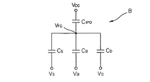
一方、前記非選択されたセルBの浮游ゲートに誘起される電圧VFGは図2に示されたセル等価回路から数式1のように表現される。
(数式1)
VFG=(CD×VD)÷(CIPO+CD+CB+CS)
【0005】
ここで、CIPOは制御ゲートと浮游ゲートとの間のキャパシタンスを示して、CDは浮游ゲートとドレーンとの間のキャパシタンスを示して、CSは浮游ゲートとソースとの間のキャパシタンスを示して、CBは浮游ゲートとバルク領域との間のキャパシタンスを示して、VDはドレーンに印加される電圧、すなわちビットラインに印加される電圧を示す。前記した数学式1は非選択されたセルBのコントロールゲート電圧VCG、ソース電圧VS及びバルク電圧VBすべてを0ボルトに仮定した場合である。
【0006】
【発明が解決しようとする課題】
前記数式1及び図2から非選択されたセルBの浮游ゲートに誘起される電圧VFGはビットラインBL1に印加される電圧に比例することが分かる。もしも非選択されたセルBが一定水準以下のスレショルド電圧(約1V)を有する過消去された(over−erased)セルの場合には、セルAをプログラムさせるためにビットラインBL1に約5ボルトの電圧を印加すれば、非選択されたセルBの浮游ゲートに所定の電圧が誘起されてセルBがターンオンされる現象が発生する。このような現象を“ドレーンターンオン(DTO;drain turn on)現象”という。前記ドレーンターンオン現象により漏洩電流、すなわちドレーンターンオン電流IDTOがビットラインBL1からセルBを通して共通ソースラインCSLに流れる。セルBがドレーンターンオン現象によりターンオンされれば、ビットラインBL1の電圧が減少して選択されたセルAがプログラムされることを難しくする。さらに、前記ドレーンターンオン電流IDTOは一本のビットラインに連結された非選択されたセルの個数が多いほどさらに増加する。また、ドレーンターンオン現象は選択されたセルAのバルク電流IBulkによってバルク電圧が増加するほど甚だしく発生する。
【0007】
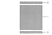
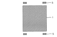
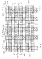
このような問題を解決するためにセルトランジスタのバルク領域にバイアスを印加してバルク領域への電流を消去してバルク電圧の増加を防止するためのバルクバイアスコンタクト構造を形成する方法が知られている。従来のバルクバイアスコンタクトは図3及び図4に示すようにセルアレー領域1の周辺を包むガードバンド(guard band)3形態で形成されたり、図5及び図6に示されているようにセルアレー領域1の4辺の角領域に対応する周辺回路領域またはセルアレー領域1の4辺中2辺の角領域に対応する周辺回路領域にバルクバイアスコンタクト構造5の形態で形成される。バルクバイアスコンタクト構造5はレイアウト面積が大きくて全体チップの面積を増加させるガードバンド3の短所を解決することができるという長所がある。しかし、バルクバイアスコンタクト構造5で遠く離れた単位セルではバルク電流の消去経路が長いためにバルク抵抗が大きくてバルク電流の消去効果が少なくて、単位セルの位置によってバルク電流の消去効果が不均一である問題点がある。
【0008】
一方、セルアレー領域のバルク電圧増加防止用バルクバイアスコンタクト構造以外にも周辺回路領域のバルク電圧を一定な電圧以下に維持するためのバルクバイアスコンタクト構造、周辺回路用トランジスタ間に生じるラッチアップ現象などを防止するためのガードバンド、静電気放電を防止するための静電気放電防止用バルクバイアスコンタクト構造などが周辺回路領域の活性領域に形成される。
【0009】
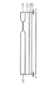
セルアレー領域や周辺回路領域のバルク電圧を一定な電圧以下に維持するための従来のバルクバイアスコンタクト構造は、図7に示すように、半導体基板10上の周辺回路領域に形成された素子分離膜30’間の活性領域に形成される。具体的に、バルクの不純物と同一な導電型の不純物が高濃度でドーピングされた領域40を露出させ、層間絶縁膜34’内に形成されたコンタクトホールを金属膜パターン50で埋め込んでバルクバイアスコンタクト構造を完成する。この時、バルクバイアスコンタクト構造の十分な接触面積を確保するためには素子分離膜30’が活性領域側に成長するバーズビークを考慮してレイアウト時活性領域の面積を増加させなければならない。すなわち、図7で実際に形成された活性領域の大きさはd1であるが、レイアウト時には活性領域の大きさをd2で配置しなければならない。したがって、バルクバイアスコンタクト構造を完成するためには所定大きさd2以上の活性領域が必要であるので、それほど全体チップの面積が増加するようになって半導体素子を高集積化することに不利になり得る。
【0010】
本発明は前記のような問題点に鑑みてなされたものであり、本発明の目的は、バルク電流を速く消去してバルク電圧を一定電圧以下に維持することができて、単位セルの位置に関係なく均一なバルク電流消去効果を有する不揮発性メモリ素子を提供することにある。
【0011】
本発明の他の目的は、バルクバイアスコンタクト構造を形成するためのレイアウト面積を最小化してチップ面積を縮小させることによって素子の高集積化を達成できる不揮発性メモリ素子を提供することにある。
【0012】
【課題を解決するための手段】
前記のような目的を達成するための本発明による不揮発性メモリ素子は、半導体基板上に相互平行した複数本のビットラインと相互平行した複数本のワードラインとが直交して、ビットラインとワードラインとに連結され、フローティングゲートとコントロールゲートとで形成された積層ゲートとソース/ドレーン領域を各々備える複数個のメモリセル及び前記ビットラインと平行した共通ソースラインを含むセルアレー領域と前記セルアレー領域の前記メモリセルを駆動するための周辺回路領域とを備える不揮発性メモリ素子として、セルアレー領域が形成されているバルク領域の電圧を一定電圧以下に維持するための少なくとも一つ以上のバルクバイアスコンタクト構造を前記セルアレー領域内に備え、前記セルアレー領域にはダミーセル及びこれらを連結する少なくとも一本以上のダミービットラインをさらに含み、少なくとも一本以上の前記ダミービットラインは、前記バルクバイアスコンタクト構造と連結されてバルクバイアスラインとして機能し、前記バルクバイアスコンタクト構造は、前記ダミーセルのソース領域およびドレーン領域に形成されたジャンクションであって、前記セルアレー領域が形成されている前記バルク領域の導電型と同一な導電型の不純物でドーピングされたバルクバイアスジャンクションとのコンタクト構造である。
【0013】
望ましくは、前記ワードライン方向に隣接した前記複数個のメモリセル及びバルクバイアスラインに属しない残りダミーセルのソース領域を連結する複数本のソースラインと前記バルクバイアスジャンクションとは所定距離離隔して形成される。
【0014】
また、前記ソースラインは、前記メモリセル及びダミーセルのソース領域間の素子分離膜を取り除いて露出した半導体基板内に形成された不純物拡散領域で構成される。
【0015】
また、前記ソースラインは、前記メモリセル及びダミーセルのソース領域間の素子分離膜上に連続的に形成されて前記ソース領域を連結する導電膜パターンで構成される。
【0016】
【発明の実施の形態】
以下、添付した図面を参照しながら本発明の実施例を説明する。しかし、本発明は以下で開示される実施例に限定されることでなく相異なる多様な形態で具現されることであり、単に本実施例は本発明の開示が完全するようにし、通常の知識を有する者に発明の範疇を完全に知らせるために提供されることである。添付された図面で多くの膜と領域の厚さとは明瞭性のために強調された。またいずれか一つの膜が他の膜または基板上に存在することと指称される時、他の膜または基板真上にある場合もあって、層間膜が存在する場合もある。
【0017】
(第1実施例)
図8に示すように、本発明の第1実施例による不揮発性メモリ素子はセルアレー領域に少なくとも一つ以上のバルクバイアスコンタクト構造80を備える。すなわち、周辺回路領域にバルクバイアスコンタクトが形成されていた従来の不揮発性メモリ素子とは別に、セルアレー領域内にバルクバイアスコンタクト構造80を備える。バルクバイアスコンタクト構造80はセルアレー領域が形成されているバルク領域の電圧を一定電圧以下に維持するためのものである。セルアレー領域には相互平行した複数本のビットラインBLと相互平行した複数本のワードラインWLとが直交する領域に形成された複数個のメモリセルがマトリックス状に配列されている。ワードラインWLと平行した方向に隣接したメモリセルのソース領域はソースラインSLに連結されており、ソースラインSLは各々共通ソースラインCSLに連結されている。望ましくは、バルクバイアスコンタクト構造80はワードラインWL方向に隣接した複数個のメモリセルのソース領域を連結する複数本のソースラインSLを連結する共通ソースラインCSLと連結される。すなわち、本発明の第1実施例による不揮発性メモリ素子は共通ソースラインCSLがバルクバイアスラインBBLとしての機能も同時に遂行するようにデザインされることが望ましい。
【0018】
共通ソースラインCSLとバルクバイアスラインBBLとを一本のラインで形成しても差し支えない理由は次のとおりである。
【0019】
セルAを選択的にプログラムさせようとする場合に、セルAと連結されたワードラインには第1電圧VPG、例えば10〜12Vの電圧を印加して、選択されたセルと連結されたビットラインには第2電圧、例えば5〜7Vの電圧を印加する。また、選択されたセルAと隣接して同一ワードラインWL1を共有したセルに連結されるビットラインBL2、BL3、およびBL4以降続くビットラインはフローティングされる。また、選択されたセルAと隣接して第2電圧が印加されたビットラインBL1とを共有するセルが連結されるワードラインWL2、WL3、およびWL4以降続くワードラインは接地される。そして、共通ソースライン及びバルクバイアスラインには第3電圧、例えば0Vの電圧を印加する。すなわち、プログラム時にソース領域とバルク領域とに同一な電圧が印加されるので共通ソースラインCSLとバルクバイアスラインBBLとを一つのラインで形成しても差し支えない。また、消去動作時にもソース領域とバルク領域とに同一電圧が印加されても消去動作には何ら影響がない。
【0020】
図9は、本発明の第1実施例による不揮発性メモリ装置セルアレー領域の一部のレイアウト図であり、図10の右側は図9のa−a’線に沿って切ったセルアレー領域の断面図で左側は周辺回路領域の断面図であり、図11は図9のb−b’線に沿って切った断面図である。
【0021】
図9、図10及び図11に示すように、半導体基板100に一方向に平行するように延びた複数個の素子分離膜130により活性領域120が定義されている。セルアレー領域はP型の基板100内に形成されたNウェル102内のポケット型P型ウェル104上に形成されて、周辺回路領域はP型の基板100’内に形成されたPウェル104’、Nウェル(図示せず)またはポケット型Pウェル(図示せず)内に形成される。セルアレー領域の活性領域120上には複数個のメモリセルが配列されている。各セルはトンネリング絶縁膜132、フローティングゲート140P、ゲート間絶縁膜134P及びコントロールゲート144Pで構成された積層ゲート構造をしている。積層ゲート間の活性領域120にはソース領域114及びドレーン領域115が形成されている。フローティングゲート140Pは活性領域120及び素子分離膜130の一部領域に渡り形成されており、ワードラインとして機能するコントロールゲート144Pは活性領域120と垂直で連続的に延びた形態で形成されている。その結果、活性領域120とコントロールゲート144Pとが直交する領域毎に一つのメモリセルが定義されて、メモリセルがマトリックス状に配列される。
【0022】
周辺回路領域の素子はゲート絶縁膜133’及びコントロールゲート144Pと同一層で構成されたゲート電極144’Pで構成された単層ゲート構造で形成され、ソース領域及びドレーン領域114’を備える。
【0023】
フローティングゲート140Pは多結晶シリコンで構成されて、コントロールゲート144Pは多結晶シリコン単一層でまたは多結晶シリコン層とシリサイド層との複合層で構成されることもできる。ゲート間絶縁膜は酸化膜と窒化膜との積層形絶縁膜(例:ONO膜)または誘電率が高い金属酸化物膜等で構成される。
【0024】
図11に示すように、コントロールゲート144P方向に隣接したメモリセルのN型ソース領域114はソース領域114間の素子分離膜130を図9のエッチングマスクパターン204を使用しコントロールゲート144Pを自己整列マスクとして用いて取り除いた後、イオン注入して形成したN型不純物拡散領域からなったソースライン116により電気的に連結される。ソースライン116は層間絶縁膜136内に形成された共通ソースラインコンタクトホール172を通して共通ソースライン190と接続する。
【0025】
セルアレー領域が形成されているバルク領域、すなわちP型ポケットウェル104の電圧を一定電圧以下に維持するためのバルクバイアスコンタクト構造は、P型ポケットウェル104内にイオン注入マスク(図9の160)を用いてP型ポケットウェル104を構成する不純物と同一不純物であるP型不純物を注入して形成したバルクバイアスジャンクション118と接続する。バルクバイアスジャンクション118を構成する不純物の濃度はP型ポケットウェル104を構成する不純物の濃度より高くドーピングすることが望ましい。バルクバイアスジャンクション118のドーピング濃度を高めることによってP型ポケットウェル104の電圧が高まることを効果的に防止できる。
【0026】
バルクバイアスジャンクション118はコントロールゲート144P間の素子分離膜130を取り除いて露出されたP型ポケットウェル104内に形成される。特に、ワードラインとして機能するコントロールゲート144P方向に隣接したドレーン領域115をつなぐ線と共通ソースライン190とが直交する領域に形成された素子分離膜130を取り除いて露出されたP型ポケットウェル104内に形成される。そして、バルクバイアスジャンクション118を露出させるバルクバイアスラインコンタクトホール174は共通ソースラインコンタクトホール172と交互に形成されている。したがって、共通ソースライン190がソースライン116と接続するのみならずバルクバイアスジャンクション118と接続してバルクバイアスラインとしての機能も同時に遂行する。
【0027】
周辺回路領域にもバルクバイアスコンタクト構造が形成されている。周辺回路領域のバルクバイアスコンタクト構造も素子分離膜130を取り除いて露出されたPウェル104’内に形成されたジャンクション114’と接触する構造で形成される。周辺回路領域の素子分離膜130を取り除いて露出されたPウェル104’内に注入される不純物の導電型はバルクバイアスコンタクトの目的によって変わることができる。例えば、バルクバイアスコンタクトがラッチアップ防止のためのガードバンド用バルクバイアスコンタクトまたは静電気放電防止用バルクバイアスコンタクトであれば、ジャンクション114’は図10に示すようにPウェル104’と反対導電型で形成されて、バルクバイアスコンタクトが素子間分離のためのガードバンド用バルクバイアスコンタクトであればPウェル104’と同一な導電型で形成される。
【0028】
本発明の第1実施例による不揮発性メモリ素子はバルクバイアスコンタクト構造をセルアレー領域内に備える。したがって、メモリセルの位置に関係なく均一で確実にセルアレー領域が形成されているバルク領域の電圧を一定電圧以下に維持することができるという長所がある。
【0029】
更に、バルクバイアスジャンクションを素子分離膜を取り除いて形成するのみならず共通ソースラインをバルクバイアスジャンクションと連結されるバルクバイアスラインとして用いる。したがって、レイアウト時セルアレー領域内にバルクバイアスラインを別設する必要がないのでレイアウト面積の増加を防止できる。
【0030】
また周辺回路領域に形成されなければならないバルクバイアスコンタクトも素子分離膜を取り除いて形成することによって、従来活性領域にバルクバイアスコンタクトを形成した方法に比べてバルクバイアスコンタクト形成のための活性領域が要らないのでチップのレイアウト面積を減少させることができる。
【0031】
(第2実施例)
図12は本発明の第2実施例による不揮発性メモリ素子のレイアウト図であり、図13は図12のb−b’線を沿って切った断面図である。
【0032】
第2実施例が第1実施例と異なる点はソースラインが不純物拡散領域(図10の116)でなく素子分離膜130上に連続的に形成されてソース領域114と接続する導電膜パターン165で構成されて、導電膜パターン165は共通ソースラインコンタクトホール172を通して共通ソースライン190と連結されることである。導電膜パターン165はポリシリコン、ポリサイドまたはタングステンのような低抵抗金属で形成される。したがって、第2実施例による不揮発性メモリ素子を製造するためにはソース領域とソース領域との間の素子分離膜を取り除くためのエッチングマスク(図9の204)が必要ない。この時、共通ソースライン190下部に形成されるソース領域114は本発明の第1実施例と同様に素子分離膜を取り除いて露出させた半導体基板に形成したり、図12及び図13に示すようにソース領域114が形成される領域に活性領域120Sに形成されることもできる。前者の場合にはソース領域114及びバルクバイアスジャンクション118が形成される領域を同時に露出させるエッチングマスクパターン(図示せず)を用いて素子分離膜を取り除いてソース領域114及びバルクバイアスジャンクション118が形成されるP型ポケットウェル104を露出させる。後者の場合にはバルクバイアスジャンクション118が形成される領域のみを露出させるエッチングマスクパターン(図12の204B)を用いて素子分離膜をエッチングしてバルクバイアスジャンクション118が形成されるP型ポケットウェル104を露出させる。
【0033】
本発明の第2実施例によると、ワードライン144P方向に隣接したメモリセルのソース領域を連結するソースラインを不純物拡散領域(図11の114)でない導電膜パターン(図13の165)で形成する。導電膜パターンで構成されたソースライン165は不純物拡散領域で構成されたソースライン114に比べて抵抗が小さい。したがって、共通ソースライン及びバルクバイアスラインCSL&BBL間に配列されるビットラインの数を第1実施例の16n(n≧1、nは整数、図9参照)個から32n(n≧1、nは整数、図12参照)個以上に増大させることができる。それゆえ、セルアレー領域内に配列される共通ソースライン及びバルクバイアスラインCSL&BBLの数を半分以下に減らすことができる。したがって、第1実施例に比べてセルアレー領域の大きさを減少させることができるという効果がある。
【0034】
(第3実施例)
図14に示すように、本発明の第3実施例による不揮発性メモリ素子はセルアレー部内に共通ソースラインCSLとは別個の独立的なバルクバイアスラインBBLを備えるという点において、第1実施例及び第2実施例と違いがある。
【0035】
本発明の第3実施例に示す配列はソースラインSLを金属ラインで形成している。本発明の第2実施例で既に説明したように、導電層パターンで構成されたソースラインSLの抵抗が小さいために二本の共通ソースライン(CSL1、CSL2)間に配列されるビットラインの数を従来の16n(n≧1、nは整数)個から32n(n≧1、nは整数)個以上に増大させることができる。それゆえ、セルアレー内に配列される共通ソースラインCSLの数字を半分以下に減らすことができる。したがって、従来に共通ソースラインCSLが形成された位置にバルクバイアスラインBBLを形成すればメモリセルアレーの面積を増加させずに、十分な数字のバルクバイアスラインBBLをセルアレー内に備えることができる。つまり、共通ソースラインCSLと共通ソースラインCSLとの中間地点にバルクバイアスラインBBLを形成することができる。したがって、バルクバイアスラインBBLと共通ソースラインCSLとの間には16n個のビットラインが配列される。
【0036】
本発明の第3実施例による不揮発性メモリ素子は、共通ソースラインCSLと独立的なバルクバイアスラインBBLとを備えるので高集積化され小型化されて低い動作電圧Vccを要する不揮発性メモリ素子に適している。動作電圧が減少するほど消去(erase)されるセルのスレショルド電圧Vth分布が図15に示すようにガウス正規分布から外れて過消去(overerase)されたテールビット(tail bit)500が形成される。このようなテールビット500により、プログラム時過消去されたセルにプログラム電流が流れるため、プログラムしようとするセルがプログラムされないプログラムフェイル(fail)が生じる。このような場合にバルクに負の電圧を印加すればセルのスレショルド電圧Vthが増加する効果があってプログラムフェイルを防止できる効果がある。したがって、ソース領域とバルクとに相異なるバイアスを印加すればプログラムフェイルを効果的に防止できる。ソース領域とバルクとに相異なるバイアスを印加するためには共通ソースラインCSL1、CSL2とバルクバイアスラインBBL1、BBL2とが各々相互独立的な端子に連結されなければならないことはもちろんである。
【0037】
例えば、セルBを選択的にプログラムさせようとする場合に、セルBと連結されたワードラインWL1に第1電圧VPG、例えば10ボルトの電圧を印加して、セルBと連結されたビットラインBL1に第2電圧、例えば約5ボルトの電圧を印加する。そして、前記選択されたセルBと隣接して同一ワードラインWL1を共有するセルが連結されるビットラインBL2、BL3、およびBL4以降続くビットラインはフローティングされる。また、前記選択されたセルBと隣接して約5ボルトの電圧が印加されたビットラインBL1を共有するセルが連結されたワードラインWL2、WL3、およびWL4以降続くワードラインは接地される。そして共通ソースラインCSL1には第3電圧、例えば0ボルトの電圧を印加して、バルクバイアスラインBBL1には第4電圧、例えば−1ボルトの電圧を印加してプログラムフェイルを効果的に防止できる。
【0038】
また、選択されたセルBとバルクバイアスラインBBL1との間の距離が近いために従来に比べて選択されたセルBのバルク電圧を一定電圧以下に効果的に維持することができる。したがって、ドレーンターンオン電流等により非選択されたセルがプログラムされる誤作動が生じない。
【0039】
必要に応じては共通ソースラインCSLとバルクバイアスラインBBLとは同一端子に連結されて電気的に連結される形態で構成される場合もある。この場合には第1実施例で説明したようにプログラム時ソース領域とバルク領域とに同一電圧が印加される。
【0040】
以下図16ないし図20を参考にして本発明の第3実施例による不揮発性メモリ素子の構造を詳細に説明する。図16は図14の一部分に対するレイアウト図であり、図17、16B、16C及び16Dは図16のa−a’線、b−b’線、c−c’線及びd−d’線を沿って切った断面図である。
【0041】
図16、図17および図20に示すように、半導体基板600のセルアレー部内に形成されて一方向に平行するように延びた複数個の素子分離領域605により複数個の活性領域610が定義されている。半導体基板600はP型の半導体基板それ自体の場合もあって、P型ウェルまたはP型の半導体基板内に形成されたNウェル内のポケット型P型ウェルの場合もあって、ここではセルアレー領域が形成されるバルク領域のみを示す。
【0042】
活性領域610上には複数個のメモリセルがマトリックス状に配列されている。各セルは、本発明の第1実施例と同様に、トンネリング絶縁膜612、フローティングゲート615、ゲート間絶縁膜617及びコントロールゲート620で構成された積層ゲート625及び積層ゲート625間の活性領域610に形成されたソース領域630及びドレーン領域635で構成される。積層ゲート625の側壁にはスペーサ627が形成されている。スペーサ627は必要によって省略することもできる。
【0043】
本発明の第1実施例と同様にフローティングゲート615は多結晶シリコンで構成されて、コントロールゲート620は多結晶シリコン単一層でまたは多結晶シリコン層618及びシリサイド層619の複合層でも構成されることができる。コントロールゲート620はワードラインとして機能する。
【0044】
そして活性領域610の一部領域にはバルクバイアスジャンクション645が形成されている。望ましくは、ワードラインとして機能するコントロールゲート620の幅方向に隣接した二つのソース領域630間の活性領域内に形成される。バルクバイアスジャンクション645はセルアレー領域が形成されているバルクにバイアスを印加するための領域である。ソース領域630及びドレーン領域635は半導体基板600と反対導電型、すなわちN型の不純物で形成されて、バルクバイアスジャンクション645は半導体基板600と同一導電型すなわちP型の不純物で形成される。望ましくは、バルクバイアスジャンクション645は半導体基板600すなわちバルク領域より高濃度でドーピングされる。ソース領域630及びドレーン領域635にはミスアラインが生じる場合起きるコンタクト抵抗の増加を防止するためのプラグイオン注入(図示せず)されていることが望ましい。
【0045】
積層ゲート625が形成されている結果物全面に第1層間絶縁膜650が形成されており、第1層間絶縁膜650内にはワードライン620方向に隣接したメモリセルのソース領域630及び素子分離領域605を連続的に露出させるソースラインコンタクトホール653、ドレーン領域635を露出させるビットラインコンタクトホール656及びバルクバイアスジャンクション645を露出させるバルクバイアスラインコンタクトホール659が形成されている。これらコンタクトホール653、656および659内には導電膜で構成されたソースライン654、ビットラインプラグ657及びバルクバイアスラインプラグ660が形成されている。ソースライン654はワードライン620方向に隣接したメモリセルのソース領域630を連結する。
【0046】
ソースライン654及びプラグ657、660が形成されている第1層間絶縁膜650上に第2層間絶縁膜670が形成されており、第2層間絶縁膜670内にはソースライン654を露出させる共通ソースラインビア673と、ビットラインプラグ657を露出させるビットラインビア676と、バルクバイアスラインプラグ660を露出させるバルクバイアスラインビア679とが形成されている。
【0047】
共通ソースラインビア673内にはソースライン654を連結し、ビットライン690と平行した共通ソースライン680とが形成されている。ビットラインビア676内にはビットラインプラグ657を通してワードライン620と垂直方向に隣接したメモリセルのドレーン領域635を連結するビットライン690が形成されている。バルクバイアスラインビア679内にはバルクバイアスジャンクション645を連結し、第2層間絶縁膜670を挟んでソースライン654と交差するバルクバイアスライン700が形成されている。
【0048】
(第4実施例)
図21に示すように、本発明の第4実施例による不揮発性メモリ素子はセルアレー領域内にメモリセルアレー領域とダミーセルアレー領域とを備え、ダミーセルアレー領域内にバルクバイアスコンタクト構造800を備える。ダミーセルアレー領域はセルアレー領域を構成するパターンを形成する時生じるローディング効果を防止するために形成する領域である。ローディング効果とはメモリ素子を製造するためのフォトエッチング工程時規則的でかつ繰り返して配列されたセルアレーパターンが変わる領域、例えばセルアレーの縁領域でパターンの臨界寸法やプロファイルが中心部領域のパターンの臨界寸法やプロファイルと変わる現象を指称する。一般的に活性領域パターン、ゲートパターンまたはビットラインパターンなどを形成する時このようなローディング効果が生じてセルの特性が脆弱になる問題点が生じる。したがって、メモリセルアレー領域の周辺にメモリセルとしては用いないダミーセルアレー領域を形成する。
【0049】
特に、本発明によるバルクバイアスコンタクト構造800は、ダミーセルアレー領域を構成するダミービットラインと連結される。すなわちダミービットラインがバルクバイアスラインBBLとして機能する。
【0050】
以下図22ないし図25を参考にして本発明の第4実施例による不揮発性メモリ素子の構造を詳細に説明する。図22は図21の一部分に対するレイアウト図であり、図23、19B及び19Cは18のa−a’線、b−b’線及びc−c’線を沿って切った断面図である。
【0051】
本発明の第4実施例による不揮発性メモリ素子は、図23に示されているように、メモリセルアレー領域のメモリセル及びビットラインは本発明の第1実施例と同一に形成されている。ただし、ダミーセルアレー領域をさらに備えて、図24に示すように、ダミービットライン190’が基板内のP型ポケットウェル104内に形成されたバルクバイアスジャンクション118と接続してバルクバイアスラインとして機能するという点において、共通ソースライン(図11の190)がバルクバイアスラインとして機能する本発明の第1実施例と差がある。バルクバイアスジャンクション118はセルアレー領域が形成されているバルク領域104の導電型と同一な導電型の不純物でドーピングされて形成される。図24ではダミービットライン190’に属するダミーセルのドレーン領域に形成されたバルクバイアスジャンクション118とダミービットライン190’とが接続してバルクバイアスラインを形成する構造が示されている。もちろんバルクバイアスジャンクション118はダミービットライン190’に属するダミーセルのソース領域にも形成されることができて、ソース領域及びドレーン領域両方すべて形成される場合もある。したがって、バルクバイアスライン190’も、ソース領域またはソース及びドレーン領域両側に形成されたバルクバイアスジャンクションに連結されることができることはもちろんである。
【0052】
図25に示すように、ワードライン144方向に隣接したソース領域114を連結するソースライン116とバルクバイアスジャンクション118とは相互に所定の間隔離隔されて形成されることが望ましい。これは図22に示されたソース、ドレーン及びソースライン用不純物拡散領域形成のためのイオン注入マスクパターン150’とバルクバイアスジャンクション形成のためのイオン注入マスクパターン160’とを所定間隔離隔されるように配置することによって形成することができる。このようにソースライン116とバルクバイアスジャンクション118とを分離させることによって、ソースライン116とバルクバイアスライン190’とに相異なる電圧が印加される場合生じることができる素子の誤作動を防止できるという効果がある。もしも素子の動作上問題がなければ、点線119で表示されたようにソースライン116とバルクバイアスジャンクション118とが連結されることもできる。
【0053】
本発明の第4実施例による不揮発性メモリ素子の変形例によると、本発明の第2実施例及び第3実施例と同様に、ダミービットラインをバルクバイアスラインとして使用し、ソースラインが不純物拡散領域でない導電膜パターンで構成されることができる。この時、前記導電膜パターンは前記バルクバイアスジャンクションと絶縁されて交差して形成されることが望ましい。
【0054】
(第5実施例)
図26ないし図43は本発明の第5実施例による不揮発性メモリ素子の製造過程を示した断面図であり、図26、図28、図30、図32、図34、図36、図38、図40および図42の右側はセルアレー領域で図9のa−a’線に沿って切った断面図を示して、左側は同じ工程段階で同時に進められる周辺回路領域の断面図を示す。また図27、図29、図31、図33、図35、図37、図39、図41、および図43は図9のb−b’線に沿って切った断面図を示す。
【0055】
図26及び図27に示すように、半導体基板100、100’にセルアレー領域と周辺回路領域が形成されるバルク領域とを形成する。バルク領域は必要なウェル102、104、104’を形成する。セルアレー領域にはP型の基板100、100’内にNウェル102及びNウェル102内にポケットPウェル104を形成して、周辺回路領域には必要によってNウェル、Pウェル104’、ポケットPウェルなどを形成する。引続き素子分離膜130、130’を形成する。
【0056】
素子分離膜130、130’は一般的に用いられるLOCOS(LocalOxidationofSilicon)やPBL(PolyBufferedLOCOS)などの素子分離器術を利用して4000Å程度の厚さで形成する。セルアレー領域では図9のレイアウトによって平行した複数個の素子分離膜130を形成する。この時、素子分離膜は共通ソースライン(図12の190)が形成される領域の全部を包むように形成する。また同時に、周辺回路領域にも必要によって素子分離膜130’を形成する。続いて、絶縁膜132、132’を形成する。絶縁膜がトンネリング膜として用いられる場合には80Åないし120Å程度の厚さに成長させる。もしも本発明による不揮発性メモリ素子がEEPROMでなくEPROMの場合には絶縁膜を200Åの厚さで形成する。この場合には絶縁膜がゲート絶縁膜として機能する。絶縁膜は一般的に酸化膜で形成する。絶縁膜132、132’を形成した後、必要に応じてはセルアレー領域のみを限定してセルのスレショルド電圧を調節するための不純物、例えばP型不純物を1.5×10¹³ないし2.5×10¹³個/cm3のイオン濃度で注入させる。
【0057】
図28及び図29に示すように、フローティングゲートを形成するための第1導電膜を形成する。第1導電膜は多結晶シリコン膜を形成した後、不純物をドーピングして導電性を高める。不純物ドーピングにはPOCl3デポジット工程またはイオン注入工程が用いられる。続いて第1導電膜をパターニングして第1導電膜パターン140を形成する。共通ソースラインが形成される領域には第1導電膜パターン140を形成しない。そして、周辺回路領域は必要によって第1導電膜パターン140’を残したり除去する。続いて、第1導電膜パターン140、140’が形成されている結果物全面にゲート間絶縁膜134、134’を形成する。ゲート間絶縁膜134、134’は酸化膜/窒化膜/酸化膜を各々50−90Å/80−120Å/50−60Åの厚さで形成したONO膜で形成することが望ましい。ONO膜厚は酸化膜に換算すれば130〜200Å程度になるようにする。
【0058】
図30及び図31に示すように、周辺回路領域のトランジスタ形成のために、セルアレー領域はマスクパターン201で保護して周辺回路領域に形成されたゲート間絶縁膜134’、第1導電膜パターン140’及び絶縁膜132’を除去する。マスクパターン201はフォトレジスト膜を用いて形成する。この時図28の段階で周辺回路領域の第1導電膜パターン142’を取り除いたならばゲート間絶縁膜134’と絶縁膜132’とのみを除去すれば良い。
【0059】
図32及び図33に示すように、図30及び図31のマスクパターン201を取り除いて、周辺回路領域の露出された基板104’上にゲート絶縁膜133’を成長した後、全面にコントロールゲート用第2導電膜144、144’を積層して、その上にマスク用絶縁膜135、135’を積層している。第2導電膜144、144’は多結晶シリコン膜の単一膜または多結晶シリコン膜とタングステンシリサイド、チタンシリサイドまたはタンタルシリサイドのような金属シリサイド膜の二重膜として形成する。マスク用絶縁膜135、135’は酸化膜、窒化膜、酸化膜と窒化膜との複合膜、酸化膜と多結晶シリコン膜との複合膜で3000〜5000Å程度の厚さで形成する。このマスク用絶縁膜135、135’の機能は後述する。
【0060】
図34及び図35に示すように、エッチング用マスクパターン202、202’を用いてマスク用絶縁膜パターン135P、135’Pを形成した後、引続きセルアレー領域にコントロールゲート144Pを、周辺回路領域には必要によってトランジスタのゲート144’Pを形成する。
【0061】
この過程は図34及び図35に示すように、エッチング用マスクパターン202、202’をマスクとしてマスク用絶縁膜135、135’と第2導電膜144、144’とを連続的にエッチングすることによって遂行することもできる。エッチング用マスクパターン202、202’を用いてマスク用絶縁膜135、135’のみをまずエッチングしてコントロールゲートを定義するマスク用絶縁膜パターン135P、135’Pを形成した後、エッチング用マスクパターン202、202’を取り除いてマスク用絶縁膜パターン135P、135’Pをマスクとして第2導電膜144、144’をエッチングしてコントロールゲート144P及び周辺回路トランジスタのゲート144’Pを形成する二段階で遂行することもできる。
【0062】
このように二段階でコントロールゲート144Pと周辺回路トランジスタのゲート144’Pとを形成する理由は次のようである。第2導電膜144、144’が多結晶シリコン膜と金属シリサイド膜との二重膜として形成された場合、厚い二重膜をエッチングするためには厚いエッチング用マスクパターン202、202’、例えば厚いフォトレジストパターンを形成しなければならない。この場合、厚いフォトレジストパターン202、202’をそのまま用いるとパターンが稠密した領域にはエッチングガスが均一に供給できずエッチングの均一度が落ちる。したがって、厚いフォトレジストパターン202、202’を取り除いた後、マスク用絶縁膜パターン135P、135’Pのみをマスクとして用いて第2導電膜144、144’をエッチングすればエッチング不均一の問題が解決される。また、このマスク用絶縁膜パターン135P、135’Pは後続工程で進められるコントロールゲート144Pの長手方向に隣接したセルのソース領域間に形成された素子分離膜130のエッチング時コントロールゲート144Pを保護する役割もする。
【0063】
図36及び図37を参照すると、周辺回路領域をマスクパターン203’で保護して、セルアレー領域に形成されたマスク用絶縁膜パターン135Pとコントロールゲート144Pとをマスクとしてゲート間絶縁膜134、第1導電膜パターン140をエッチングしてフローティングゲート140P、ゲート間絶縁膜パターン134P及びコントロールゲート144Pで構成された積層ゲートを完成する。この時、共通ソースラインが形成される素子分離膜130上にもゲート間絶縁膜パターン134P、コントロールゲート144P及びマスク用絶縁膜パターン135Pが順序とおり積層されている構造物が形成される。ここでコントロールゲート144Pと周辺回路トランジスタのゲート144’Pとをマスクとして基板上にLDD用N型不純物を注入できる。
【0064】
図38及び図39に示すように、図9のソースライン用不純物拡散領域とバルクバイアスジャンクションが形成される半導体基板領域を露出させるためのエッチングマスクパターン204とを利用してセルアレー領域のドレーン領域とコントロールゲート144Pとの一部を包みながらソースラインとバルクバイアスコンタクトジャンクションとが形成される領域にある素子分離膜130を露出すると同時に、周辺回路領域の一部素子分離膜130’も露出するマスクパターン204、204’を形成する。
【0065】
このマスクパターン204を用いて素子分離膜130、130’をエッチングすれば、セルアレー領域ではコントロールゲート144Pとその上に積層されたマスク用絶縁膜パターン135Pとにより自己整列されて、コントロールゲート144Pの長手方向に隣接したセルのソース領域間の素子分離膜130が取り除かれてソースラインが形成される領域とバルクバイアスコンタクトジャンクションが形成される領域とが露出される。この時、コントロールゲート144P上に積層されているマスク用絶縁膜パターン135Pが素子分離膜130エッチング時コントロールゲート144Pが損傷されることを防止する。また、図38に示すように周辺回路領域の素子分離膜130’の一部も取り除かれて周辺回路用バルクバイアスジャンクションが形成される領域が露出される。前記素子分離膜130、130’のエッチング工程前または後に積層ゲートの側壁にスペーサ(図示せず)を形成する工程をさらに実施することもできる。望ましくは、素子分離膜130、130’のエッチング工程前にスペーサを形成する。
【0066】
図40及び図41を参照すると、ソースライン用不純物拡散領域及びバルクバイアスジャンクション形成用マスクパターン204、204’を取り除いてソース、ドレーン領域及びソースライン用不純物拡散領域を形成するためのイオンとバルクバイアスジャンクションを形成するためのイオンとを注入する。イオン注入過程は二段階に分けて実施する。まず、セルアレー領域中ソースとドレーン領域及びソースライン用不純物拡散領域が形成される領域を限定すると同時に周辺回路領域中NMOSトランジスタのソースとドレーン領域及びN+ガードバンドを形成する領域を限定するイオン注入マスクパターン(図9の150)を利用して基板100、100’上にN型イオン注入マスクパターン(図示せず)を形成した後、N+不純物、例えばヒ素(As)やリン(P)を注入する(108、108’)。N型イオン注入マスクパターンを取り除いた後、セルアレー領域中バルクバイアスジャンクションが形成される領域及び周辺回路領域中PMOSトランジスタのソースとドレーン領域及びP+ガードバンドを形成する領域を限定するパターン(図9の160)を利用してP型イオン注入マスクパターン(図示せず)を形成した後、P+不純物、例えばホウ素(B)やニフッ化ホウ素(BF2)を注入する(110)。
【0067】
図40で周辺回路領域中素子分離膜130’が取り除かれた位置に注入される不純物の導電型がN+であって、その下のPウェル104’と反対の導電型として示されているが、この導電型はこの部分に形成される周辺回路用バルクバイアスコンタクトの目的によって変わることもできる。すなわち、この部分に形成されるバルクバイアスコンタクトがラッチアップ防止のためのガードバンド用コンタクトまたは静電気放電防止用コンタクトであれば、図40に示すようにPウェル104’と反対導電型としてイオン注入して、素子間分離のためのガードバンド用バルクバイアスコンタクトであればPウェル104’と同一な導電型としてイオン注入できる。
【0068】
図42及び図43に示すように、イオン注入後全面に層間絶縁膜136、136’として高温酸化膜とBPSGとを各々1000Åおよび5000Å程度に積層して900℃程度の温度でリフローさせ平坦化する。続いて、層間絶縁膜136をエッチングしてセルアレー領域中ビットラインコンタクトホール170、共通ソースラインコンタクトホール172及びバルクバイアスラインコンタクトホール174、周辺回路用バルクバイアスジャンクションを露出させるコンタクトホール170’を形成する。続いて金属または金属シリサイドなどの導電層を積層してエッチングしてセルアレー領域のドレーン領域115と接続するビットライン180、ソースライン114及びバルクバイアスジャンクション118と同時に接続する共通ソースライン及びバルクバイアスライン190及び周辺回路領域の配線180’を完成する。
【0069】
(第6実施例)
図44ないし図63は本発明の第6実施例による不揮発性メモリ素子の製造工程を示す。
【0070】
図44ないし図47に示すように、基板600内にセルアレー領域と周辺回路領域とが形成されるバルク領域を形成して、素子分離膜605を形成して活性領域を限定して、活性領域上にトンネリング酸化膜612、フローティングゲート615、ゲート間絶縁膜617及び多結晶シリコン膜618及びシリサイド膜619の二重膜で構成されたコントロールゲート620からなった積層ゲート625を形成する工程までは第5実施例による不揮発性メモリ素子の製造方法と同一に実施する。ただし共通ソースライン(図16の700)が形成される領域が素子分離膜上に定義されることでなく活性領域(図16の610)上に定義されるという点においてのみ違いがある。次に積層ゲート625が形成された結果物全面に酸化膜、窒化膜または多結晶シリコン膜を形成した後、エッチバックして積層ゲート625の側壁にスペーサ627を形成する。
【0071】
引き続き、積層ゲート625が形成された結果物上にソース及びドレーン領域形成用マスクパターン629を形成する。マスクパターン629はフォトレジストを塗布した後これをパターニングして形成する。このマスクパターン629をイオン注入マスクとして用いてN型不純物を注入してソース領域630及びドレーン領域635を形成する。その結果複数個のメモリセルが基板600上にマトリックス状に配列される。
【0072】
図48ないし図51に示すように、ソース/ドレーン領域630、635形成用イオン注入マスクパターン629を取り除いた後、図16に示すバルクバイアスジャンクション領域を定義するイオン注入マスクパターン640を形成する。マスクパターン640はコントロールゲート620の幅方向に隣接した二つのソース630領域間の活性領域を露出させる。このマスクパターン640をイオン注入マスクとして用いてP型の不純物をイオン注入して複数個のバルクバイアスジャンクション645を形成する。
【0073】
図52ないし図55に示すように、バルクバイアスジャンクション645を定義するイオン注入マスクパターン640を取り除いた後、基板600全面に第1層間絶縁膜650を形成する。まず高温酸化膜を基板600全面に500Åないし1000Å厚さで形成した後、高温酸化膜上にBPSG膜を4000Åないし6000Å厚さで順序とおり蒸着する。続いてBPSG膜を850℃ないし900℃で10ないし20分間リフローして平坦化させて第1層間絶縁膜650を形成する。
【0074】
続いて、第1層間絶縁膜650上にソースラインコンタクトホール、ビットラインコンタクトホール及びバルクバイアスラインコンタクトホールを定義するマスクパターン651を形成する。マスクパターン651はフォトレジスト膜を塗布した後パターニングして形成する。マスクパターン651をエッチングマスクとして用いて第1層間絶縁膜650をエッチングしてソース領域630及び素子分離領域605をコントロールゲート、すなわちワードライン620の長手方向に連続的に露出させるソースラインコンタクトホール653、ドレーン領域635を各々露出させるビットラインコンタクトホール656及びバルクバイアスジャンクション645を各々露出させるバルクバイアスラインコンタクトホール659を形成する。
【0075】
図56ないし図59に示すように、コンタクトホール653、656、659を定義するマスクパターン651を取り除いた後、コンタクトホール653、656、659を埋め込む第1導電膜を形成する。第1導電膜は金属、金属シリサイドまたは多結晶シリコン等の導電物質で形成される。特に、抵抗が低い導電物質、例えば、タングステンを用いて形成することが望ましい。第1導電膜を形成した後、これをエッチバックまたは化学機械的研磨で平坦化してソースラインコンタクトホール653内にはソースライン654を、ビットラインコンタクトホール656内にはビットラインプラグ657を、バルクバイアスラインコンタクトホール659内にはバルクバイアスラインプラグ660を各々形成する。したがって、ソースライン654は図59に示すように、ワードライン620方向に隣接したセルのソース領域630を連結するようになる。
【0076】
引き続き、ソースライン654、ビットラインプラグ657及びバルクバイアスラインプラグ660が形成された結果物全面に第2層間絶縁膜670を形成する。第2層間絶縁膜670は酸化物などを用いて形成する。引続き、第2層間絶縁膜670上にビアホール形成用マスクパターン671を形成する。ビアホール形成用マスクパターン671もフォトレジストを塗布した後パターニングして形成する。
【0077】
ビアホール形成用マスクパターン671をエッチングマスクとして用いて第2層間絶縁膜670をエッチングしてソースライン654を各々露出させる複数個の共通ソースラインビアホール673、ビットラインプラグ657を各々露出させる複数本のビットラインビアホール676及びバルクバイアスラインプラグ660を各々露出させる複数個のバルクバイアスラインビアホール679を各々形成する。
【0078】
図60から図63を参照すると、ビアホール形成用マスクパターン671を取り除いた後前記ビアホール673、676、679を各々埋め込んで前記第2層間絶縁膜670上に一定厚さになるように第2導電膜を形成する。
第2導電膜は金属、金属シリサイドまたはポリサイドを用いて形成する。引続き第2導電膜をパターニングしてソースライン654を連結する複数個の共通ソースライン680、ワードライン620と垂直方向に隣接したドレーン領域635とを連結する複数本のビットライン690及び活性領域内に形成されたバルクバイアスジャンクション645を連結し、ソースライン654と交差する複数個のバルクバイアスライン700を完成する。
【0079】
(第7実施例)
本発明の第7実施例による不揮発性メモリ素子の製造工程は本発明の第5実施例による不揮発性メモリ素子の製造工程と大部分の工程において同一に進められる。ただし、共通ソースラインをバルクバイアスラインとして形成することでなく、共通ソースラインはセルアレー領域内の活性領域上に形成して、メモリセルアレー領域の周辺部にローディング効果を減少させるためにダミーセルアレー領域をさらに形成してダミーセルアレー領域に形成されるダミービットラインをバルクバイアスラインとして形成するという点においてのみ違いがある。
【0080】
以下、図64から図69を参考にして本発明の第7実施例による不揮発性メモリ素子の製造工程を説明する。図64及び図67は図22のa−a’線に沿って切った断面図であり、図65及び図68は図22のb−b’線に沿って切った断面図であり、図66及び図69は図22のc−c’線に沿って切った断面図である。
【0081】
具体的に、半導体基板100に必要なウェル102、104、を形成してセルアレー領域と周辺回路部が形成されるバルク領域とを定義して、素子分離膜を形成してメモリセルが形成される活性領域とダミーセルが形成される活性領域とを定義した後、トンネリング絶縁膜132、フローティングゲート140P及びゲート間絶縁膜134P及びコントロールゲート144Pで構成された積層ゲートを形成して、ソースライン用不純物拡散領域形成用エッチングマスクパターン(図22の204’)を用いた自己整列エッチング工程を実施してコントロールゲート144P、すなわちワードラインの長さ方向に隣接したソース領域間の素子分離膜をエッチングする段階までは本発明の第5実施例と同一に進める。
【0082】
本発明の第7実施例によるソースライン用不純物拡散領域形成用エッチングマスクパターン(図22の204’)は、不純物拡散領域が形成される領域のみ定義してバルクバイアスジャンクションが形成される領域は定義しないという点においてのみ第1実施例のパターン(図9の204)と差がある。
【0083】
引き続き、ソース、ドレーン及びソースライン用不純物拡散領域形成用イオン注入マスクパターン(図22の150’)を用いて基板100上にイオン注入マスクパターン(図示せず)を形成する。このイオン注入マスクパターンはダミーセルアレー領域中、バルクバイアスジャンクションが形成される領域のみ遮って残りダミーセル領域とメモリセル領域とを露出させる。イオン注入マスクパターンを用いてN型不純物イオンを注入してソース領域114及びドレーン領域115とソースライン用不純物拡散領域116とを形成する。
【0084】
続いて、積層ゲート形成のためのエッチング工程及び前記イオン注入時受けたトンネリング絶縁膜の損傷を回復して注入されたN型不純物が積層ゲートの縁と適切にオーバーラップされるように所望する深さまで拡散させるために熱処理工程を進める。この熱処理工程は必要に応じて省略されることもある。
【0085】
次に、バルクバイアスジャンクション形成用イオン注入マスクパターン(図22の160’)を用いて基板上にイオン注入マスクパターン(図示せず)を形成する。このイオン注入マスクパターンは周辺回路部のPジャンクションを一緒に定義することもできる。このイオン注入マスクパターンを用いてP型不純物例えば、ニフッ化ホウ素などをイオン注入して図61に示すようにダミーセルのドレーン領域及びソース領域にバルクバイアスジャンクション118を形成する。もちろんバルクバイアスジャンクション118はダミーセルのドレーン領域にのみまたはソース領域にのみ形成される場合もある。
【0086】
望ましくは、バルクバイアスジャンクションを定義するイオン注入マスクパターン(図22の160’)とソース、ドレーン領域及びソースライン用不純物拡散領域を定義するイオン注入マスクパターン(図22の150’)は所定距離離隔されて配置されて図66に示すようにソースライン用不純物拡散領域116とバルクバイアスジャンクション118とが分離されるように形成することが望ましい。
【0087】
以後、図67から図69に示すように、層間絶縁膜136を形成した後、フォトエッチング工程を利用してビットラインコンタクトホール170、ダミービットラインコンタクトホール(図22の172)及びバルクバイアスラインコンタクトホール174を各々形成して、導電膜を浸せき及びパターニングしてビットライン180、ダミービットライン182及びバルクバイアスラインとして機能するダミービットライン190’を形成する工程は用いるパターンの形態のみ異なるのみ本発明の第5実施例と実質的に同一な方式で進める。
【0088】
【発明の効果】
本発明による不揮発性メモリ素子によるとセルアレー部内にバルクバイアスコンタクト構造を備える。したがって、メモリセルの位置に関係なく均一で確実にセルアレー領域が形成されているバルク領域の電圧を一定電圧以下に維持することができるという効果がある。
【0089】
バルクバイアスジャンクションを素子分離膜を取り除いて露出された半導体基板内に形成して共通ソースラインをバルクコンタクトジャンクションと連結されるバルクバイアスラインに用いる場合にはレイアウト時セルアレー領域内にバルクバイアスラインを別設する必要がない。
【0090】
一方、金属ラインで構成されたソースラインを備える場合には従来に比べて少ない数の共通ソースラインを形成しても素子特性をそのまま維持することができるのでバルクバイアスラインを従来の共通ソースライン位置に配列させることができる。
【0091】
更に、ローディング効果を減少させるために形成するダミーセルアレー領域もバルクバイアスコンタクト構造を形成する領域として用いることができる。
【0092】
すなわち、本発明による不揮発性メモリ素子はメモリセルアレーの面積は増大させずにセルとバルクバイアスコンタクトとの間の距離を著しく減少させることができる効果がある。したがって、メモリセルが形成されているバルクの電圧を一定電圧以下に効果的に維持することができる。
【0093】
また周辺回路領域に形成されなければならないバルクバイアスコンタクトも素子分離膜を取り除いて形成することによって、従来活性領域にバルクバイアスコンタクトを形成した方法に比べてバルクバイアスコンタクト形成のための活性領域が要らないのでチップのレイアウト面積を減少させることができる。
【0094】
特に、素子分離膜を取り除いてその席にバルクバイアスコンタクトを形成するようになれば、チップ設計後製造されたチップを評価した結果バルクバイアスコンタクトと関連して誤差が生じてレイアウトを変更しても最初工程、すなわち素子分離膜を形成してバルクバイアスコンタクトが形成される活性領域を定義する工程から再び遂行する必要なくワードラインを形成した後、素子分離膜を取り除く工程から再び遂行すれば良いので、工程検証時間が縮まってそれによって開発期間も縮まるという利点がある。
【図面の簡単な説明】
【図1】不揮発性メモリ素子のプログラム時、非選択されたセルのドレーンターンオン現象を説明するための等価回路図である。
【図2】図1に示すセルBの等価回路図である。
【図3】従来の不揮発性メモリ素子においてセルアレー領域とバルクバイアスコンタクト構造間の位置を説明するための平面図である。
【図4】従来の不揮発性メモリ素子においてセルアレー領域とバルクバイアスコンタクト構造間の位置を説明するための平面図である。
【図5】従来の不揮発性メモリ素子においてセルアレー領域とバルクバイアスコンタクト構造間の位置を説明するための平面図である。
【図6】従来の不揮発性メモリ素子においてセルアレー領域とバルクバイアスコンタクト構造間の位置を説明するための平面図である。
【図7】従来の素子分離膜間の活性領域にバルクバイアスコンタクトを形成した場合を示した断面図である。
【図8】本発明の第1実施例による不揮発性メモリ素子のセルアレー領域の等価回路図である。
【図9】図8のセルアレー領域の一部分に対するレイアウト図である。
【図10】図9のa−a’線に沿って切った断面図である。
【図11】図9のb−b’線に沿って切った断面図である。
【図12】本発明の第2実施例による不揮発性メモリ素子のセルアレー領域の一部分に対するレイアウト図である。
【図13】図12のb−b’線に沿って切った断面図である。
【図14】本発明の第3実施例による不揮発性メモリ素子のセルアレー領域の等価回路図である
【図15】プログラム及び消去動作時セルのスレショルド電圧分布を示すグラフである。
【図16】図14のセルアレー領域の一部分に対するレイアウト図である。
【図17】図16のa−a’線に沿って切った断面図である。
【図18】図16のb−b’線に沿って切った断面図である。
【図19】図16のc−c’線に沿って切った断面図である。
【図20】図16のd−d’線に沿って切った断面図である。
【図21】本発明の第4実施例による不揮発性メモリ素子のセルアレー領域の等価回路図である。
【図22】図21のセルアレー領域の一部分に対するレイアウト図である。
【図23】図22のa−a’線に沿って切った断面図である。
【図24】図22のb−b’線に沿って切った断面図である。
【図25】図22のc−c’線に沿って切った断面図である。
【図26】本発明の第5実施例による不揮発性メモリ素子の製造方法を示した断面図である。
【図27】本発明の第5実施例による不揮発性メモリ素子の製造方法を示した断面図である。
【図28】本発明の第5実施例による不揮発性メモリ素子の製造方法を示した断面図である。
【図29】本発明の第5実施例による不揮発性メモリ素子の製造方法を示した断面図である。
【図30】本発明の第5実施例による不揮発性メモリ素子の製造方法を示した断面図である。
【図31】本発明の第5実施例による不揮発性メモリ素子の製造方法を示した断面図である。
【図32】本発明の第5実施例による不揮発性メモリ素子の製造方法を示した断面図である。
【図33】本発明の第5実施例による不揮発性メモリ素子の製造方法を示した断面図である。
【図34】本発明の第5実施例による不揮発性メモリ素子の製造方法を示した断面図である。
【図35】本発明の第5実施例による不揮発性メモリ素子の製造方法を示した断面図である。
【図36】本発明の第5実施例による不揮発性メモリ素子の製造方法を示した断面図である。
【図37】本発明の第5実施例による不揮発性メモリ素子の製造方法を示した断面図である。
【図38】本発明の第5実施例による不揮発性メモリ素子の製造方法を示した断面図である。
【図39】本発明の第5実施例による不揮発性メモリ素子の製造方法を示した断面図である。
【図40】本発明の第5実施例による不揮発性メモリ素子の製造方法を示した断面図である。
【図41】本発明の第5実施例による不揮発性メモリ素子の製造方法を示した断面図である。
【図42】本発明の第5実施例による不揮発性メモリ素子の製造方法を示した断面図である。
【図43】本発明の第5実施例による不揮発性メモリ素子の製造方法を示した断面図である。
【図44】本発明の第6実施例による不揮発性メモリ素子の製造方法を示した断面図である。
【図45】本発明の第6実施例による不揮発性メモリ素子の製造方法を示した断面図である。
【図46】本発明の第6実施例による不揮発性メモリ素子の製造方法を示した断面図である。
【図47】本発明の第6実施例による不揮発性メモリ素子の製造方法を示した断面図である。
【図48】本発明の第6実施例による不揮発性メモリ素子の製造方法を示した断面図である。
【図49】本発明の第6実施例による不揮発性メモリ素子の製造方法を示した断面図である。
【図50】本発明の第6実施例による不揮発性メモリ素子の製造方法を示した断面図である。
【図51】本発明の第6実施例による不揮発性メモリ素子の製造方法を示した断面図である。
【図52】本発明の第6実施例による不揮発性メモリ素子の製造方法を示した断面図である。
【図53】本発明の第6実施例による不揮発性メモリ素子の製造方法を示した断面図である。
【図54】本発明の第6実施例による不揮発性メモリ素子の製造方法を示した断面図である。
【図55】本発明の第6実施例による不揮発性メモリ素子の製造方法を示した断面図である。
【図56】本発明の第6実施例による不揮発性メモリ素子の製造方法を示した断面図である。
【図57】本発明の第6実施例による不揮発性メモリ素子の製造方法を示した断面図である。
【図58】本発明の第6実施例による不揮発性メモリ素子の製造方法を示した断面図である。
【図59】本発明の第6実施例による不揮発性メモリ素子の製造方法を示した断面図である。
【図60】本発明の第6実施例による不揮発性メモリ素子の製造方法を示した断面図である。
【図61】本発明の第6実施例による不揮発性メモリ素子の製造方法を示した断面図である。
【図62】本発明の第6実施例による不揮発性メモリ素子の製造方法を示した断面図である。
【図63】本発明の第6実施例による不揮発性メモリ素子の製造方法を示した断面図である。
【図64】本発明の第7実施例による不揮発性メモリ素子の製造方法を示した断面図である。
【図65】本発明の第7実施例による不揮発性メモリ素子の製造方法を示した断面図である。
【図66】本発明の第7実施例による不揮発性メモリ素子の製造方法を示した断面図である。
【図67】本発明の第7実施例による不揮発性メモリ素子の製造方法を示した断面図である。
【図68】本発明の第7実施例による不揮発性メモリ素子の製造方法を示した断面図である。
【図69】本発明の第7実施例による不揮発性メモリ素子の製造方法を示した断面図である。
【符号の説明】
10 半導体基板
30 素子分離膜
34 層間絶縁膜
40 領域
50 金属膜パターン
80 バルクバイアスコンタクト構造
100 基板
100 半導体基板
102 ウェル
104 ポケット型P型ウェル
114 ソース領域
115 ドレーン領域
116 ソースライン
118 バルクバイアスジャンクション
120 活性領域
130 素子分離膜
132 トンネリング絶縁膜
134P ゲート間絶縁膜
135 マスク用絶縁膜
136 層間絶縁膜
140 導電膜パターン
165 ソースライン
170 コンタクトホール
180 ビットライン
190 ダミービットライン
201 マスクパターン
202 フォトレジストパターン[0001]
BACKGROUND OF THE INVENTION
The present invention relates to a nonvolatile memory device and a manufacturing method thereof, and more particularly, to a nonvolatile memory device having a bulk bias contact structure in a cell array region and a manufacturing method thereof.
[0002]
[Prior art]
Nonvolatile memory devices are widely used in computers, memory cards, and the like because they have a feature that information stored in memory cells is not lost even when power is not supplied.
[0003]
A phenomenon affecting the operation characteristics of these nonvolatile memory elements will be described with reference to FIG. 1 which is a partially enlarged circuit diagram of the nonvolatile memory elements. When the cell indicated by the reference symbol A is to be selectively programmed, the program voltage V is applied to the selected word line WL1 connected to the cell A.PGFor example, a voltage of 10 to 15 volts is applied, and a voltage of about 5 volts is applied to the selected bit line BL1 connected to the cell A. Then, the non-selected bit line BL2 connected to the cell adjacent to the selected cell A and sharing the same word line WL1 is floated. Further, the non-selected word line WL2 connected to the cell B sharing the bit line BL1 to which the voltage of about 5 volts is applied adjacent to the selected cell A is grounded. When the cell A is selectively programmed, the electric field in the channel direction is remarkably increased in the pinch-off region near the drain in the channel region under the gate of the selected cell A. These electrons are accelerated by this strong electric field and easily enter a high energy state. The electrons in the high energy state collide with the silicon lattice in the bulk region near the drain and generate a large number of electron-hole pairs. Electrons generated by impact ionization and some of the electrons with high energy in the holes are injected into the floating gate through the tunnel oxide film by the gate electric field, and most of the remaining electrons are pulled by the high drain electric field and flow into the drain. And become part of the drain current. At this time, the holes are pushed out by the drain electric field and flow into the source terminal or the bulk terminal through the depletion layer or the bulk region under the channel. Thus, the hole current through the drain and bulk region of the selected cell A, i.e. the bulk current IBulkFlows. Bulk current IBulkIs the bulk resistance RBulkTo increase the bulk voltage. Bulk resistance RBulkIf the bulk voltage becomes 0.6 V or more, the source region which is the ground node and the PN junction between the substrates are forward-biased to generate an undesired forward current, and the cell current rapidly increases. Causes a snap-back phenomenon. As a result, the cell may not operate normally or an excessive current may break the cell junction.
[0004]
Meanwhile, the voltage V induced in the floating gate of the non-selected cell BFGIs expressed by
(Formula 1)
VFG= (CD× VD) ÷ (CIPO+ CD+ CB+ CS)
[0005]
Where CIPOIndicates the capacitance between the control gate and the floating gate, and CDIndicates the capacitance between the floating gate and the drain, and CSIndicates the capacitance between the floating gate and the source, CBIndicates the capacitance between the floating gate and the bulk region and VDIndicates a voltage applied to the drain, that is, a voltage applied to the bit line. The above
[0006]
[Problems to be solved by the invention]
The voltage V induced at the floating gate of the cell B not selected from
[0007]
In order to solve such a problem, a method of forming a bulk bias contact structure for applying a bias to a bulk region of a cell transistor to erase a current to the bulk region and preventing an increase in bulk voltage is known. Yes. A conventional bulk bias contact is formed in the form of a
[0008]
On the other hand, in addition to the bulk bias contact structure for preventing the bulk voltage increase in the cell array region, the bulk bias contact structure for maintaining the bulk voltage in the peripheral circuit region below a certain voltage, the latch-up phenomenon that occurs between the peripheral circuit transistors, etc. A guard band for preventing, an electrostatic discharge preventing bulk bias contact structure for preventing electrostatic discharge, and the like are formed in the active region of the peripheral circuit region.
[0009]
As shown in FIG. 7, a conventional bulk bias contact structure for maintaining the bulk voltage in the cell array region and the peripheral circuit region below a certain voltage is an
[0010]
The present invention has been made in view of the above-described problems, and an object of the present invention is to quickly erase the bulk current and maintain the bulk voltage below a certain voltage, so that the unit cell is positioned. It is an object of the present invention to provide a non-volatile memory device having a uniform bulk current erasing effect.
[0011]
Another object of the present invention is to provide a non-volatile memory device capable of achieving high device integration by minimizing the layout area for forming the bulk bias contact structure and reducing the chip area.
[0012]
[Means for Solving the Problems]
In order to achieve the above object, a nonvolatile memory device according to the present invention includes a plurality of bit lines parallel to each other and a plurality of word lines parallel to each other on a semiconductor substrate. A plurality of memory cells each including a stacked gate formed by a floating gate and a control gate and a source / drain region, and a cell array region including a common source line parallel to the bit line and the cell array region. As a nonvolatile memory device having a peripheral circuit region for driving the memory cell, at least one bulk bias contact structure for maintaining the voltage of the bulk region in which the cell array region is formed below a certain voltageThe cell array region further includes a dummy cell and at least one dummy bit line connecting the dummy cells, and the at least one dummy bit line is connected to the bulk bias contact structure. The bulk bias contact structure is a junction formed in a source region and a drain region of the dummy cell and has the same conductivity type as that of the bulk region in which the cell array region is formed. This is a contact structure with a bulk bias junction doped with impurities.
[0013]
PreferablyThe plurality of source lines that connect the source regions of the plurality of memory cells adjacent to the word line direction and the remaining dummy cells that do not belong to the bulk bias line and the bulk bias junction are formed at a predetermined distance.
[0014]
The source line may be an impurity diffusion region formed in the semiconductor substrate exposed by removing an element isolation film between the source regions of the memory cell and the dummy cell.
[0015]
The source line is formed of a conductive film pattern that is continuously formed on an isolation layer between the source regions of the memory cell and the dummy cell and connects the source regions.
[0016]
DETAILED DESCRIPTION OF THE INVENTION
Hereinafter, embodiments of the present invention will be described with reference to the accompanying drawings. However, the present invention is not limited to the embodiments disclosed below, but may be embodied in various different forms. The embodiments are merely intended to ensure that the disclosure of the present invention is complete. It is provided to fully inform those who have the scope of the invention. In the accompanying drawings, many film and region thicknesses have been emphasized for clarity. Further, when any one film is referred to as being present on another film or substrate, the film may be directly on the other film or substrate or an interlayer film may be present.
[0017]
(First embodiment)
As shown in FIG. 8, the non-volatile memory device according to the first embodiment of the present invention includes at least one bulk
[0018]
The reason why the common source line CSL and the bulk bias line BBL may be formed as a single line is as follows.
[0019]
When the cell A is to be selectively programmed, the word line connected to the cell A has a first voltage VPGFor example, a voltage of 10 to 12V is applied, and a second voltage, for example, a voltage of 5 to 7V, is applied to the bit line connected to the selected cell. In addition, bit lines BL2, BL3, and BL4 that are connected to a cell adjacent to the selected cell A and sharing the same word line WL1 are floated. In addition, word lines WL2, WL3, and word lines subsequent to WL4 to which cells sharing the selected cell A and sharing the bit line BL1 to which the second voltage is applied are connected are grounded. A third voltage, for example, a voltage of 0 V is applied to the common source line and the bulk bias line. That is, since the same voltage is applied to the source region and the bulk region during programming, the common source line CSL and the bulk bias line BBL may be formed as one line. Even during the erase operation, even if the same voltage is applied to the source region and the bulk region, the erase operation is not affected at all.
[0020]
FIG. 9 is a layout view of a part of the cell array region of the nonvolatile memory device according to the first embodiment of the present invention, and the right side of FIG. 10 is a cross-sectional view of the cell array region taken along the line aa ′ of FIG. The left side is a cross-sectional view of the peripheral circuit region, and FIG. 11 is a cross-sectional view taken along the line bb ′ of FIG.
[0021]
As shown in FIGS. 9, 10, and 11, the
[0022]
The element in the peripheral circuit region is formed of a single-layer gate structure including a gate electrode 144'P formed of the same layer as the
[0023]
The floating
[0024]
As shown in FIG. 11, the N-
[0025]
In the bulk region where the cell array region is formed, that is, the bulk bias contact structure for maintaining the voltage of the P-type pocket well 104 below a certain voltage, an ion implantation mask (160 in FIG. 9) is provided in the P-
[0026]
The
[0027]
A bulk bias contact structure is also formed in the peripheral circuit region. The bulk bias contact structure in the peripheral circuit region is also formed in a structure in contact with the
[0028]
The nonvolatile memory device according to the first embodiment of the present invention includes a bulk bias contact structure in the cell array region. Therefore, there is an advantage that the voltage of the bulk region in which the cell array region is formed can be maintained at a constant voltage or less regardless of the position of the memory cell.
[0029]
Further, the bulk bias junction is formed by removing the element isolation film, and the common source line is used as a bulk bias line connected to the bulk bias junction. Therefore, since it is not necessary to separately provide a bulk bias line in the cell array region during layout, an increase in layout area can be prevented.
[0030]
Also, the bulk bias contact that must be formed in the peripheral circuit region is formed by removing the element isolation film, so that an active region for forming the bulk bias contact is required as compared with the conventional method in which the bulk bias contact is formed in the active region. Therefore, the chip layout area can be reduced.
[0031]
(Second embodiment)
FIG. 12 is a layout view of a nonvolatile memory device according to a second embodiment of the present invention, and FIG. 13 is a cross-sectional view taken along the line b-b 'of FIG.
[0032]
The second embodiment is different from the first embodiment in that the source line is not formed in the impurity diffusion region (116 in FIG. 10), but is formed continuously on the
[0033]
According to the second embodiment of the present invention, the source line connecting the source regions of the memory cells adjacent in the direction of the
[0034]
(Third embodiment)
As shown in FIG. 14, the non-volatile memory device according to the third embodiment of the present invention includes the first embodiment and the second embodiment in that the cell array unit includes an independent bulk bias line BBL separate from the common source line CSL. There are differences from the second embodiment.
[0035]
In the arrangement shown in the third embodiment of the present invention, the source line SL is formed of a metal line. As already described in the second embodiment of the present invention, the number of bit lines arranged between the two common source lines (CSL1, CSL2) because the resistance of the source line SL formed of the conductive layer pattern is small. Can be increased from 16n (n ≧ 1, n is an integer) to 32n (n ≧ 1, n is an integer) or more. Therefore, the number of common source lines CSL arranged in the cell array can be reduced to less than half. Therefore, if the bulk bias line BBL is formed at the position where the common source line CSL is conventionally formed, a sufficient number of bulk bias lines BBL can be provided in the cell array without increasing the area of the memory cell array. That is, the bulk bias line BBL can be formed at an intermediate point between the common source line CSL and the common source line CSL. Accordingly, 16n bit lines are arranged between the bulk bias line BBL and the common source line CSL.
[0036]
The non-volatile memory device according to the third embodiment of the present invention includes a common source line CSL and an independent bulk bias line BBL. Therefore, the non-volatile memory device is highly integrated, miniaturized, and suitable for a non-volatile memory device requiring a low operating voltage Vcc. ing. As the operating voltage decreases, the threshold voltage Vth distribution of the erased cell deviates from the Gaussian normal distribution as shown in FIG. 15, and a
[0037]
For example, when the cell B is selectively programmed, the first voltage V1 is applied to the word line WL1 connected to the cell B.PGFor example, a voltage of 10 volts is applied, and a second voltage, for example, a voltage of about 5 volts, is applied to the bit line BL1 connected to the cell B. Then, bit lines BL2, BL3, and BL4 and subsequent bit lines connected to cells sharing the same word line WL1 adjacent to the selected cell B are floated. In addition, word lines WL2, WL3, and word lines subsequent to WL4 to which cells sharing bit line BL1 to which a voltage of about 5 volts is applied adjacent to the selected cell B are connected are grounded. Then, a third voltage, for example, a voltage of 0 volts is applied to the common source line CSL1, and a fourth voltage, for example, a voltage of -1 volt is applied to the bulk bias line BBL1, thereby effectively preventing a program failure.
[0038]
Further, since the distance between the selected cell B and the bulk bias line BBL1 is short, the bulk voltage of the selected cell B can be effectively maintained below a certain voltage as compared with the conventional case. Therefore, a malfunction in which a non-selected cell is programmed by a drain turn-on current or the like does not occur.
[0039]
If necessary, the common source line CSL and the bulk bias line BBL may be connected to the same terminal and electrically connected. In this case, as described in the first embodiment, the same voltage is applied to the source region during programming and the bulk region.
[0040]
Hereinafter, the structure of the nonvolatile memory device according to the third embodiment of the present invention will be described in detail with reference to FIGS. FIG. 16 is a layout diagram for a part of FIG. 14, and FIGS. 17, 16B, 16C and 16D are taken along lines aa ′, bb ′, cc ′ and dd ′ of FIG. It is sectional drawing cut off.
[0041]
As shown in FIGS. 16, 17 and 20, a plurality of
[0042]
A plurality of memory cells are arranged in a matrix on the
[0043]
Similar to the first embodiment of the present invention, the floating
[0044]
A
[0045]
A first
[0046]
A second
[0047]
In the common source line via 673, a
[0048]
(Fourth embodiment)
As shown in FIG. 21, the nonvolatile memory device according to the fourth embodiment of the present invention includes a memory cell array region and a dummy cell array region in the cell array region, and a bulk
[0049]
In particular, the bulk
[0050]
Hereinafter, the structure of the nonvolatile memory device according to the fourth embodiment of the present invention will be described in detail with reference to FIGS. FIG. 22 is a layout diagram for a part of FIG. 21, and FIGS. 23, 19B and 19C are cross-sectional views taken along 18 a-a ', b-b' and c-c 'lines.
[0051]
In the nonvolatile memory device according to the fourth embodiment of the present invention, as shown in FIG. 23, the memory cells and bit lines in the memory cell array region are formed in the same manner as in the first embodiment of the present invention. However, a dummy cell array region is further provided, and as shown in FIG. 24, a
[0052]
As shown in FIG. 25, the
[0053]
According to a modification of the non-volatile memory device according to the fourth embodiment of the present invention, the dummy bit line is used as a bulk bias line and the source line is impurity diffused, as in the second and third embodiments of the present invention. A conductive film pattern that is not a region can be used. At this time, it is preferable that the conductive film pattern is formed to be insulated from the bulk bias junction.
[0054]
(5th Example)
26 to 43 are cross-sectional views illustrating a process of manufacturing a nonvolatile memory device according to a fifth embodiment of the present invention. FIGS. 26, 28, 30, 32, 34, 36, 38, The right side of FIGS. 40 and 42 shows a cross-sectional view taken along the line aa ′ of FIG. 9 in the cell array region, and the left side shows a cross-sectional view of the peripheral circuit region simultaneously advanced in the same process step. 27, 29, 31, 33, 35, 37, 39, 41, and 43 are cross-sectional views taken along the line b-b 'of FIG.
[0055]
As shown in FIGS. 26 and 27, a cell array region and a bulk region in which a peripheral circuit region is formed are formed in the
[0056]
The
[0057]
As shown in FIGS. 28 and 29, a first conductive film for forming a floating gate is formed. After forming a polycrystalline silicon film, the first conductive film is doped with impurities to improve conductivity. POCl for impurity doping3A deposition process or an ion implantation process is used. Subsequently, the first conductive film is patterned to form a first
[0058]
As shown in FIGS. 30 and 31, in order to form transistors in the peripheral circuit region, the cell array region is protected by a
[0059]
As shown in FIGS. 32 and 33, after removing the
[0060]
As shown in FIGS. 34 and 35, after forming the mask insulating
[0061]
As shown in FIGS. 34 and 35, this process is performed by continuously etching the
[0062]
The reason why the
[0063]
Referring to FIGS. 36 and 37, the peripheral circuit region is protected by a mask pattern 203 ′, and the inter-gate
[0064]
As shown in FIGS. 38 and 39, the drain region of the cell array region is formed using the impurity diffusion region for source line of FIG. 9 and the
[0065]
If the
[0066]
Referring to FIGS. 40 and 41, ions and bulk bias for removing source line impurity diffusion regions and bulk bias junction
[0067]
In FIG. 40, the conductivity type of the impurity implanted at the position where the
[0068]
As shown in FIGS. 42 and 43, after ion implantation, a high-temperature oxide film and BPSG are laminated as interlayer insulating
[0069]
(Sixth embodiment)
44 to 63 show a manufacturing process of the nonvolatile memory device according to the sixth embodiment of the present invention.
[0070]
As shown in FIGS. 44 to 47, a bulk region in which a cell array region and a peripheral circuit region are formed is formed in a
[0071]
Subsequently, a source and drain region forming
[0072]
As shown in FIGS. 48 to 51, after removing the ion
[0073]
As shown in FIGS. 52 to 55, after removing the ion
[0074]
Subsequently, a
[0075]
As shown in FIGS. 56 to 59, after removing the
[0076]
Subsequently, a second
[0077]
Using the via hole forming
[0078]
Referring to FIGS. 60 to 63, after the via hole forming
The second conductive film is formed using metal, metal silicide, or polycide. Subsequently, a plurality of
[0079]
(Seventh embodiment)
The manufacturing process of the non-volatile memory device according to the seventh embodiment of the present invention is the same as the manufacturing process of the non-volatile memory device according to the fifth embodiment of the present invention. However, instead of forming the common source line as a bulk bias line, the common source line is formed on the active region in the cell array region to reduce the loading effect in the peripheral portion of the memory cell array region. Is further formed only in that dummy bit lines formed in the dummy cell array region are formed as bulk bias lines.
[0080]
Hereinafter, a manufacturing process of the nonvolatile memory device according to the seventh embodiment of the present invention will be described with reference to FIGS. 64 and 67 are cross-sectional views taken along the line aa ′ of FIG. 22, and FIGS. 65 and 68 are cross-sectional views taken along the line bb ′ of FIG. 69 is a cross-sectional view taken along the line cc ′ of FIG.
[0081]
Specifically,
[0082]
The source line impurity diffusion region forming etching mask pattern (204 ′ in FIG. 22) according to the seventh embodiment of the present invention defines only the region where the impurity diffusion region is formed and defines the region where the bulk bias junction is formed. It is different from the pattern of the first embodiment (204 in FIG. 9) only in that it is not.
[0083]
Subsequently, an ion implantation mask pattern (not shown) is formed on the
[0084]
Subsequently, an etching process for forming the stacked gate and a desired depth so that the N-type impurity implanted by appropriately recovering the damage of the tunneling insulating film received during the ion implantation may be overlapped with the edge of the stacked gate. The heat treatment process is advanced in order to diffuse the film. This heat treatment step may be omitted as necessary.
[0085]
Next, an ion implantation mask pattern (not shown) is formed on the substrate using the ion implantation mask pattern for bulk bias junction formation (160 'in FIG. 22). This ion implantation mask pattern can also define the P junction of the peripheral circuit portion together. Using this ion implantation mask pattern, a P-type impurity such as boron difluoride is ion-implanted to form a
[0086]
Preferably, an ion implantation mask pattern (160 'in FIG. 22) defining a bulk bias junction and an ion implantation mask pattern (150' in FIG. 22) defining a source, drain region, and source line impurity diffusion region are separated by a predetermined distance. As shown in FIG. 66, the source line
[0087]
Thereafter, as shown in FIGS. 67 to 69, after an
[0088]
【The invention's effect】
The nonvolatile memory device according to the present invention includes a bulk bias contact structure in the cell array portion. Therefore, there is an effect that the voltage of the bulk region in which the cell array region is formed uniformly and surely can be maintained below a certain voltage regardless of the position of the memory cell.
[0089]
When the bulk bias junction is formed in the exposed semiconductor substrate with the device isolation film removed and the common source line is used as a bulk bias line connected to the bulk contact junction, the bulk bias line is separated in the cell array region during layout. There is no need to install.
[0090]
On the other hand, when a source line composed of a metal line is provided, the device characteristics can be maintained as they are even if a smaller number of common source lines are formed than in the conventional case. Can be arranged.
[0091]
Further, a dummy cell array region formed to reduce the loading effect can also be used as a region for forming a bulk bias contact structure.
[0092]
That is, the nonvolatile memory device according to the present invention has an effect that the distance between the cell and the bulk bias contact can be remarkably reduced without increasing the area of the memory cell array. Therefore, the bulk voltage in which the memory cells are formed can be effectively maintained below a certain voltage.
[0093]
Also, the bulk bias contact that must be formed in the peripheral circuit region is formed by removing the element isolation film, so that an active region for forming the bulk bias contact is required as compared with the conventional method in which the bulk bias contact is formed in the active region. Therefore, the chip layout area can be reduced.
[0094]
In particular, if the device isolation film is removed and a bulk bias contact is formed at the seat, evaluation of the chip manufactured after the chip design results in an error associated with the bulk bias contact and changes in the layout. Since the word line is formed after the first step, that is, the step of defining the active region where the bulk bias contact is formed by forming the element isolation film, it is sufficient to perform again from the step of removing the element isolation film. There is an advantage that the process verification time is shortened, thereby shortening the development period.
[Brief description of the drawings]
FIG. 1 is an equivalent circuit diagram for explaining a drain turn-on phenomenon of a non-selected cell during programming of a nonvolatile memory device.
FIG. 2 is an equivalent circuit diagram of the cell B shown in FIG.
FIG. 3 is a plan view for explaining a position between a cell array region and a bulk bias contact structure in a conventional nonvolatile memory device.
FIG. 4 is a plan view for explaining a position between a cell array region and a bulk bias contact structure in a conventional nonvolatile memory device.
FIG. 5 is a plan view illustrating a position between a cell array region and a bulk bias contact structure in a conventional nonvolatile memory device.
FIG. 6 is a plan view for explaining a position between a cell array region and a bulk bias contact structure in a conventional nonvolatile memory device.
FIG. 7 is a cross-sectional view showing a case where a bulk bias contact is formed in an active region between conventional element isolation films.
FIG. 8 is an equivalent circuit diagram of a cell array region of the nonvolatile memory device according to the first embodiment of the present invention.
9 is a layout diagram for a part of the cell array region of FIG. 8;
10 is a cross-sectional view taken along the line a-a ′ of FIG. 9;
11 is a cross-sectional view taken along the line b-b ′ in FIG. 9;
FIG. 12 is a layout view illustrating a part of a cell array region of a nonvolatile memory device according to a second embodiment of the present invention.
13 is a cross-sectional view taken along line b-b ′ of FIG.
FIG. 14 is an equivalent circuit diagram of a cell array region of a nonvolatile memory device according to a third embodiment of the present invention.
FIG. 15 is a graph showing a threshold voltage distribution of a cell during a program and erase operation.
16 is a layout diagram for a part of the cell array region of FIG. 14;
17 is a cross-sectional view taken along line a-a ′ of FIG. 16;
FIG. 18 is a cross-sectional view taken along line b-b ′ of FIG.
19 is a cross-sectional view taken along line c-c ′ of FIG. 16;
20 is a cross-sectional view taken along the line d-d ′ in FIG. 16;
FIG. 21 is an equivalent circuit diagram of a cell array region of a nonvolatile memory device according to a fourth embodiment of the present invention.
22 is a layout diagram for a part of the cell array region of FIG. 21;
23 is a cross-sectional view taken along line a-a ′ of FIG.
24 is a cross-sectional view taken along line b-b ′ of FIG.
25 is a cross-sectional view taken along line c-c ′ of FIG.
FIG. 26 is a cross-sectional view illustrating a method of manufacturing a non-volatile memory device according to a fifth embodiment of the present invention.
FIG. 27 is a cross-sectional view illustrating a method of manufacturing a non-volatile memory device according to a fifth embodiment of the present invention.
FIG. 28 is a cross-sectional view illustrating a method of manufacturing a non-volatile memory device according to a fifth embodiment of the present invention.
FIG. 29 is a cross-sectional view illustrating a method of manufacturing a non-volatile memory device according to a fifth embodiment of the present invention.
FIG. 30 is a cross-sectional view illustrating a method of manufacturing a nonvolatile memory device according to a fifth embodiment of the present invention.
FIG. 31 is a cross-sectional view illustrating a method of manufacturing a non-volatile memory device according to a fifth embodiment of the present invention.
FIG. 32 is a cross-sectional view illustrating a method of manufacturing a nonvolatile memory device according to a fifth embodiment of the present invention.
FIG. 33 is a cross-sectional view illustrating a method for manufacturing a nonvolatile memory device in accordance with a fifth embodiment of the present invention.
FIG. 34 is a cross-sectional view illustrating a method for manufacturing a nonvolatile memory device in accordance with a fifth embodiment of the present invention.
FIG. 35 is a cross-sectional view showing a method of manufacturing a nonvolatile memory device in accordance with a fifth embodiment of the present invention.
FIG. 36 is a cross-sectional view showing a method of manufacturing a nonvolatile memory device in accordance with a fifth embodiment of the present invention.
FIG. 37 is a cross-sectional view illustrating a method of manufacturing a non-volatile memory device according to a fifth embodiment of the present invention.
FIG. 38 is a cross-sectional view showing a method of manufacturing a nonvolatile memory device in accordance with a fifth embodiment of the present invention.
FIG. 39 is a cross-sectional view illustrating a method of manufacturing a non-volatile memory device according to a fifth embodiment of the present invention.
FIG. 40 is a cross-sectional view illustrating a method of manufacturing a non-volatile memory device according to a fifth embodiment of the present invention.
FIG. 41 is a cross-sectional view showing a method of manufacturing a nonvolatile memory device in accordance with a fifth embodiment of the present invention.
FIG. 42 is a cross-sectional view showing a method of manufacturing a nonvolatile memory device in accordance with a fifth embodiment of the present invention.
FIG. 43 is a cross-sectional view showing a method of manufacturing a nonvolatile memory device in accordance with a fifth embodiment of the present invention.
FIG. 44 is a cross-sectional view illustrating a method of manufacturing a nonvolatile memory device according to a sixth embodiment of the present invention.
FIG. 45 is a cross-sectional view showing a method of manufacturing a nonvolatile memory device in accordance with a sixth embodiment of the present invention.
FIG. 46 is a cross-sectional view showing a method of manufacturing a nonvolatile memory device according to a sixth example of the present invention.
FIG. 47 is a cross-sectional view showing a method of manufacturing a nonvolatile memory device in accordance with the sixth embodiment of the present invention.
FIG. 48 is a cross-sectional view showing a method of manufacturing a nonvolatile memory device in accordance with a sixth embodiment of the present invention.
FIG. 49 is a cross-sectional view showing a method of manufacturing a nonvolatile memory device according to a sixth example of the present invention.
FIG. 50 is a cross-sectional view showing a method of manufacturing a nonvolatile memory device in accordance with a sixth embodiment of the present invention.
FIG. 51 is a cross-sectional view showing a method of manufacturing a nonvolatile memory device in accordance with a sixth embodiment of the present invention.
FIG. 52 is a cross-sectional view showing a method of manufacturing a nonvolatile memory device according to a sixth example of the present invention.
FIG. 53 is a cross-sectional view showing a method of manufacturing a nonvolatile memory device in accordance with a sixth embodiment of the present invention.
FIG. 54 is a cross-sectional view showing a method of manufacturing a nonvolatile memory device according to a sixth example of the present invention.
FIG. 55 is a cross-sectional view showing a method of manufacturing a nonvolatile memory device in accordance with the sixth embodiment of the present invention.
FIG. 56 is a cross-sectional view showing a method for manufacturing a nonvolatile memory device in accordance with a sixth embodiment of the present invention.
FIG. 57 is a cross-sectional view showing a method for manufacturing a nonvolatile memory device in accordance with a sixth embodiment of the present invention.
FIG. 58 is a cross-sectional view showing a method of manufacturing a nonvolatile memory device in accordance with a sixth embodiment of the present invention.
FIG. 59 is a cross-sectional view showing a method of manufacturing a nonvolatile memory device according to a sixth example of the present invention.
FIG. 60 is a cross-sectional view illustrating a method for manufacturing a nonvolatile memory device in accordance with a sixth embodiment of the present invention.
FIG. 61 is a cross-sectional view showing a method for manufacturing a nonvolatile memory device in accordance with a sixth embodiment of the present invention.
FIG. 62 is a cross-sectional view showing a method of manufacturing a nonvolatile memory device in accordance with the sixth embodiment of the present invention.
FIG. 63 is a cross-sectional view illustrating a method for manufacturing a nonvolatile memory device in accordance with a sixth embodiment of the present invention.
FIG. 64 is a cross-sectional view showing a method of manufacturing a nonvolatile memory device in accordance with a seventh embodiment of the present invention.
FIG. 65 is a cross-sectional view illustrating a method for manufacturing a nonvolatile memory device in accordance with a seventh embodiment of the present invention.
FIG. 66 is a cross-sectional view showing a method of manufacturing a nonvolatile memory device in accordance with a seventh embodiment of the present invention.
FIG. 67 is a cross-sectional view showing a method of manufacturing a nonvolatile memory device in accordance with the seventh embodiment of the present invention.
FIG. 68 is a cross-sectional view illustrating a method for manufacturing a nonvolatile memory device in accordance with a seventh embodiment of the present invention.
FIG. 69 is a cross-sectional view illustrating a method for manufacturing a nonvolatile memory device in accordance with a seventh embodiment of the present invention.
[Explanation of symbols]
10 Semiconductor substrate
30 element isolation membrane
34 Interlayer insulation film
40 areas
50 Metal film pattern
80 Bulk bias contact structure
100 substrates
100 Semiconductor substrate
102 wells
104 pocket type P type well
114 Source region
115 Drain area
116 source line
118 Bulk bias junction
120 active region
130 Device isolation membrane
132 Tunneling insulating film
134P Inter-gate insulating film
135 Insulating film for mask
136 Interlayer insulation film
140 Conductive film pattern
165 source line
170 contact hole
180 bit line
190 Dummy bit line
201 Mask pattern
202 photoresist pattern
Claims (4)
前記セルアレー領域が形成されているバルク領域の電圧を一定電圧以下に維持するための少なくとも一つ以上のバルクバイアスコンタクト構造を前記セルアレー領域内に備え、
前記セルアレー領域にはダミーセル及びこれらを連結する少なくとも一本以上のダミービットラインをさらに含み、
少なくとも一本以上の前記ダミービットラインは、前記バルクバイアスコンタクト構造と連結されてバルクバイアスラインとして機能し、
前記バルクバイアスコンタクト構造は、前記ダミーセルのソース領域およびドレーン領域に形成されたジャンクションであって、前記セルアレー領域が形成されている前記バルク領域の導電型と同一な導電型の不純物でドーピングされたバルクバイアスジャンクションとのコンタクト構造であることを特徴とする不揮発性メモリ素子。A stacked gate composed of a floating gate and a control gate, wherein a plurality of bit lines parallel to each other and a plurality of word lines parallel to each other are orthogonally connected to each other on the semiconductor substrate. A non-volatile memory device including a plurality of memory cells each including a source / drain region, a cell array region including a common source line parallel to the bit line, and a peripheral circuit region for driving the memory cells in the cell array region In
At least one bulk bias contact structure for maintaining the voltage of the bulk region in which the cell array region is formed below a certain voltage is provided in the cell array region,
The cell array region further includes dummy cells and at least one dummy bit line connecting the dummy cells,
At least one dummy bit line is connected to the bulk bias contact structure and functions as a bulk bias line .
The bulk bias contact structure is a junction formed in a source region and a drain region of the dummy cell and is doped with an impurity having the same conductivity type as that of the bulk region in which the cell array region is formed. A non-volatile memory device having a contact structure with a bias junction .
Applications Claiming Priority (2)
| Application Number | Priority Date | Filing Date | Title |
|---|---|---|---|
| KR1999P36330 | 1999-08-30 | ||
| KR1019990036330A KR100304710B1 (en) | 1999-08-30 | 1999-08-30 | Nonovolatile Memory Device Having Bulk Bias Contact Structure in Cell Array Region |
Publications (2)
| Publication Number | Publication Date |
|---|---|
| JP2001110920A JP2001110920A (en) | 2001-04-20 |
| JP4463954B2 true JP4463954B2 (en) | 2010-05-19 |
Family
ID=19609250
Family Applications (1)
| Application Number | Title | Priority Date | Filing Date |
|---|---|---|---|
| JP2000260509A Expired - Fee Related JP4463954B2 (en) | 1999-08-30 | 2000-08-30 | Nonvolatile memory device having bulk bias contact structure in cell array region |
Country Status (3)
| Country | Link |
|---|---|
| US (1) | US6483749B1 (en) |
| JP (1) | JP4463954B2 (en) |
| KR (1) | KR100304710B1 (en) |
Families Citing this family (32)
| Publication number | Priority date | Publication date | Assignee | Title |
|---|---|---|---|---|
| JP2003007869A (en) * | 2001-06-26 | 2003-01-10 | Fujitsu Ltd | Semiconductor device and manufacturing method thereof |
| JP3831277B2 (en) | 2001-12-28 | 2006-10-11 | 株式会社東芝 | Semiconductor device |
| JP4647175B2 (en) | 2002-04-18 | 2011-03-09 | ルネサスエレクトロニクス株式会社 | Semiconductor integrated circuit device |
| CN100452403C (en) * | 2002-12-30 | 2009-01-14 | 旺宏电子股份有限公司 | Structure of non-volatile memory and its operation method |
| JP4163610B2 (en) * | 2003-12-22 | 2008-10-08 | 株式会社東芝 | Nonvolatile semiconductor memory device |
| JP4817615B2 (en) * | 2004-05-31 | 2011-11-16 | 株式会社東芝 | Nonvolatile semiconductor memory device |
| KR100604875B1 (en) | 2004-06-29 | 2006-07-31 | 삼성전자주식회사 | Non-volatile semiconductor memory device having a strap region and manufacturing method thereof |
| KR100689830B1 (en) * | 2005-05-09 | 2007-03-08 | 삼성전자주식회사 | Semiconductor integrated circuits and manufacturing methods thereof |
| JP4287400B2 (en) * | 2005-03-31 | 2009-07-01 | 株式会社東芝 | Semiconductor integrated circuit device |
| JP2006344900A (en) | 2005-06-10 | 2006-12-21 | Toshiba Corp | Semiconductor device |
| US7151302B1 (en) | 2005-06-24 | 2006-12-19 | Freescale Semiconductor, Inc. | Method and apparatus for maintaining topographical uniformity of a semiconductor memory array |
| KR100624962B1 (en) * | 2005-07-04 | 2006-09-15 | 주식회사 하이닉스반도체 | Manufacturing Method of Flash Memory Device |
| JP5135815B2 (en) * | 2006-02-14 | 2013-02-06 | ミツミ電機株式会社 | Semiconductor integrated circuit device |
| TWI311351B (en) * | 2006-08-21 | 2009-06-21 | Powerchip Semiconductor Corp | Method of manufacturing well pick-up structure of non-volatile memory |
| US7439134B1 (en) * | 2007-04-20 | 2008-10-21 | Freescale Semiconductor, Inc. | Method for process integration of non-volatile memory cell transistors with transistors of another type |
| JP5700907B2 (en) * | 2008-06-26 | 2015-04-15 | ピーエスフォー ルクスコ エスエイアールエルPS4 Luxco S.a.r.l. | Semiconductor memory device |
| US7919792B2 (en) * | 2008-12-18 | 2011-04-05 | Taiwan Semiconductor Manufacturing Company, Ltd. | Standard cell architecture and methods with variable design rules |
| JP5197406B2 (en) * | 2009-01-27 | 2013-05-15 | 株式会社東芝 | Semiconductor memory device |
| US8541832B2 (en) | 2009-07-23 | 2013-09-24 | Samsung Electronics Co., Ltd. | Integrated circuit memory devices having vertical transistor arrays therein and methods of forming same |
| JP4977180B2 (en) | 2009-08-10 | 2012-07-18 | 株式会社東芝 | Method for manufacturing nonvolatile semiconductor memory device |
| KR101624975B1 (en) | 2009-11-17 | 2016-05-30 | 삼성전자주식회사 | Three dimensional semiconductor memory devices |
| KR101623547B1 (en) * | 2009-12-15 | 2016-05-23 | 삼성전자주식회사 | Method for manufacturing rewriteable three dimensional memory device |
| KR20120003351A (en) | 2010-07-02 | 2012-01-10 | 삼성전자주식회사 | 3D nonvolatile memory device and its operation method |
| KR101763420B1 (en) | 2010-09-16 | 2017-08-01 | 삼성전자주식회사 | Therr dimensional semiconductor memory devices and methods of fabricating the same |
| KR101825539B1 (en) | 2010-10-05 | 2018-03-22 | 삼성전자주식회사 | Three Dimensional Semiconductor Memory Device And Method Of Fabricating The Same |
| KR102633141B1 (en) * | 2016-12-07 | 2024-02-02 | 삼성전자주식회사 | Integrated circuit devices |
| US10249378B1 (en) * | 2017-11-09 | 2019-04-02 | Winbond Electronics Corp. | Flash memory device and method for recovering over-erased memory cells |
| KR20180058673A (en) | 2018-04-24 | 2018-06-01 | 포항공과대학교 산학협력단 | 3d sram core cell having vertical stacking structure and core cell assembly compring the same |
| US11289500B2 (en) * | 2019-08-06 | 2022-03-29 | Samsung Electronics Co., Ltd. | Memory device |
| KR102738686B1 (en) * | 2019-08-06 | 2024-12-09 | 삼성전자주식회사 | Memory device |
| KR200493800Y1 (en) | 2021-03-12 | 2021-06-09 | 노경수 | Garland pedestal |
| US12125523B2 (en) * | 2022-01-27 | 2024-10-22 | Taiwan Semiconductor Manufacturing Company, Ltd. | Memory device and method of manufacturing the same |
Family Cites Families (9)
| Publication number | Priority date | Publication date | Assignee | Title |
|---|---|---|---|---|
| US5120671A (en) | 1990-11-29 | 1992-06-09 | Intel Corporation | Process for self aligning a source region with a field oxide region and a polysilicon gate |
| JP2870284B2 (en) * | 1991-02-15 | 1999-03-17 | 日本電気株式会社 | Electrically erasable nonvolatile semiconductor memory device |
| US5470773A (en) | 1994-04-25 | 1995-11-28 | Advanced Micro Devices, Inc. | Method protecting a stacked gate edge in a semiconductor device from self aligned source (SAS) etch |
| US5595925A (en) * | 1994-04-29 | 1997-01-21 | Texas Instruments Incorporated | Method for fabricating a multiple well structure for providing multiple substrate bias for DRAM device formed therein |
| JP3376204B2 (en) * | 1996-02-15 | 2003-02-10 | 株式会社東芝 | Semiconductor device |
| KR100225758B1 (en) * | 1996-09-13 | 1999-10-15 | 윤종용 | Nonvolatile semiconductor memory cell with lockable cells |
| KR100255148B1 (en) * | 1997-08-30 | 2000-05-01 | 김영환 | Flash memory cell array |
| US6002610A (en) * | 1998-04-30 | 1999-12-14 | Lucent Technologies Inc. | Non-volatile memory element for programmable logic applications and operational methods therefor |
| US6160737A (en) * | 1998-08-10 | 2000-12-12 | Aplus Flash Technology, Inc. | Bias conditions for repair, program and erase operations of non-volatile memory |
-
1999
- 1999-08-30 KR KR1019990036330A patent/KR100304710B1/en not_active Expired - Fee Related
-
2000
- 2000-08-29 US US09/650,493 patent/US6483749B1/en not_active Expired - Lifetime
- 2000-08-30 JP JP2000260509A patent/JP4463954B2/en not_active Expired - Fee Related
Also Published As
| Publication number | Publication date |
|---|---|
| US6483749B1 (en) | 2002-11-19 |
| KR20010019754A (en) | 2001-03-15 |
| JP2001110920A (en) | 2001-04-20 |
| KR100304710B1 (en) | 2001-11-01 |
Similar Documents
| Publication | Publication Date | Title |
|---|---|---|
| JP4463954B2 (en) | Nonvolatile memory device having bulk bias contact structure in cell array region | |
| US6757199B2 (en) | Nonvolatile memory structures and fabrication methods | |
| JP4065310B2 (en) | Method for manufacturing nonvolatile memory device using self-align source process | |
| US8344443B2 (en) | Single poly NVM devices and arrays | |
| US5953254A (en) | Serial flash memory | |
| US6821847B2 (en) | Nonvolatile memory structures and fabrication methods | |
| KR19990016013A (en) | Cell Array Structure of Nonvolatile Semiconductor Memory Device and Manufacturing Method Thereof | |
| KR100297728B1 (en) | Method for fabricating flash memory device and flash memory device fabricated thereby | |
| US5409854A (en) | Method for forming a virtual-ground flash EPROM array with floating gates that are self aligned to the field oxide regions of the array | |
| US7553725B2 (en) | Nonvolatile memory devices and methods of fabricating the same | |
| US6902974B2 (en) | Fabrication of conductive gates for nonvolatile memories from layers with protruding portions | |
| US6846712B2 (en) | Fabrication of gate dielectric in nonvolatile memories having select, floating and control gates | |
| KR100273705B1 (en) | Method for fabricating of nonvolatile memory device and well structure thereof | |
| KR100673226B1 (en) | Manufacturing method of nonvolatile memory device | |
| US6628550B1 (en) | Structure, fabrication and operation method of flash memory device | |
| JP3947041B2 (en) | Semiconductor device and manufacturing method thereof | |
| KR20040010550A (en) | Lowered channel doping with source side boron implant for deep sub 0.18 micron flash memory cell | |
| US20040084718A1 (en) | Structure, fabrication method and operation method of flash memory | |
| JP4291076B2 (en) | Method of manufacturing an EEPROM element with a simple manufacturing process | |
| US6778438B2 (en) | Structure, fabrication method and operating method for flash memory |
Legal Events
| Date | Code | Title | Description |
|---|---|---|---|
| A621 | Written request for application examination |
Free format text: JAPANESE INTERMEDIATE CODE: A621 Effective date: 20051109 |
|
| A977 | Report on retrieval |
Free format text: JAPANESE INTERMEDIATE CODE: A971007 Effective date: 20080227 |
|
| A131 | Notification of reasons for refusal |
Free format text: JAPANESE INTERMEDIATE CODE: A131 Effective date: 20090916 |
|
| A601 | Written request for extension of time |
Free format text: JAPANESE INTERMEDIATE CODE: A601 Effective date: 20091216 |
|
| A602 | Written permission of extension of time |
Free format text: JAPANESE INTERMEDIATE CODE: A602 Effective date: 20091221 |
|
| A521 | Request for written amendment filed |
Free format text: JAPANESE INTERMEDIATE CODE: A523 Effective date: 20091225 |
|
| TRDD | Decision of grant or rejection written | ||
| A01 | Written decision to grant a patent or to grant a registration (utility model) |
Free format text: JAPANESE INTERMEDIATE CODE: A01 Effective date: 20100128 |
|
| A01 | Written decision to grant a patent or to grant a registration (utility model) |
Free format text: JAPANESE INTERMEDIATE CODE: A01 |
|
| A61 | First payment of annual fees (during grant procedure) |
Free format text: JAPANESE INTERMEDIATE CODE: A61 Effective date: 20100218 |
|
| FPAY | Renewal fee payment (event date is renewal date of database) |
Free format text: PAYMENT UNTIL: 20130226 Year of fee payment: 3 |
|
| R150 | Certificate of patent or registration of utility model |
Ref document number: 4463954 Country of ref document: JP Free format text: JAPANESE INTERMEDIATE CODE: R150 Free format text: JAPANESE INTERMEDIATE CODE: R150 |
|
| FPAY | Renewal fee payment (event date is renewal date of database) |
Free format text: PAYMENT UNTIL: 20140226 Year of fee payment: 4 |
|
| R250 | Receipt of annual fees |
Free format text: JAPANESE INTERMEDIATE CODE: R250 |
|
| R250 | Receipt of annual fees |
Free format text: JAPANESE INTERMEDIATE CODE: R250 |
|
| R250 | Receipt of annual fees |
Free format text: JAPANESE INTERMEDIATE CODE: R250 |
|
| R250 | Receipt of annual fees |
Free format text: JAPANESE INTERMEDIATE CODE: R250 |
|
| R250 | Receipt of annual fees |
Free format text: JAPANESE INTERMEDIATE CODE: R250 |
|
| R250 | Receipt of annual fees |
Free format text: JAPANESE INTERMEDIATE CODE: R250 |
|
| R250 | Receipt of annual fees |
Free format text: JAPANESE INTERMEDIATE CODE: R250 |
|
| LAPS | Cancellation because of no payment of annual fees |