JP4425730B2 - コネクタ端子の製造方法 - Google Patents
コネクタ端子の製造方法 Download PDFInfo
- Publication number
- JP4425730B2 JP4425730B2 JP2004195101A JP2004195101A JP4425730B2 JP 4425730 B2 JP4425730 B2 JP 4425730B2 JP 2004195101 A JP2004195101 A JP 2004195101A JP 2004195101 A JP2004195101 A JP 2004195101A JP 4425730 B2 JP4425730 B2 JP 4425730B2
- Authority
- JP
- Japan
- Prior art keywords
- terminal
- connector
- connector terminal
- press
- bending
- Prior art date
- Legal status (The legal status is an assumption and is not a legal conclusion. Google has not performed a legal analysis and makes no representation as to the accuracy of the status listed.)
- Expired - Fee Related
Links
- 238000004519 manufacturing process Methods 0.000 title claims description 15
- 239000000463 material Substances 0.000 claims description 42
- 238000005452 bending Methods 0.000 claims description 34
- 238000004080 punching Methods 0.000 claims description 9
- 239000002184 metal Substances 0.000 claims description 6
- 238000000465 moulding Methods 0.000 claims description 3
- 239000000758 substrate Substances 0.000 description 20
- 238000000034 method Methods 0.000 description 19
- 238000003825 pressing Methods 0.000 description 11
- 230000000149 penetrating effect Effects 0.000 description 2
- 238000005476 soldering Methods 0.000 description 2
- 230000015572 biosynthetic process Effects 0.000 description 1
- 238000005520 cutting process Methods 0.000 description 1
- 238000010586 diagram Methods 0.000 description 1
- 230000002452 interceptive effect Effects 0.000 description 1
- 239000002994 raw material Substances 0.000 description 1
- 230000008961 swelling Effects 0.000 description 1
- 229920003002 synthetic resin Polymers 0.000 description 1
- 239000000057 synthetic resin Substances 0.000 description 1
Images


Classifications
-
- H—ELECTRICITY
- H01—ELECTRIC ELEMENTS
- H01R—ELECTRICALLY-CONDUCTIVE CONNECTIONS; STRUCTURAL ASSOCIATIONS OF A PLURALITY OF MUTUALLY-INSULATED ELECTRICAL CONNECTING ELEMENTS; COUPLING DEVICES; CURRENT COLLECTORS
- H01R43/00—Apparatus or processes specially adapted for manufacturing, assembling, maintaining, or repairing of line connectors or current collectors or for joining electric conductors
- H01R43/16—Apparatus or processes specially adapted for manufacturing, assembling, maintaining, or repairing of line connectors or current collectors or for joining electric conductors for manufacturing contact members, e.g. by punching and by bending
-
- H—ELECTRICITY
- H01—ELECTRIC ELEMENTS
- H01R—ELECTRICALLY-CONDUCTIVE CONNECTIONS; STRUCTURAL ASSOCIATIONS OF A PLURALITY OF MUTUALLY-INSULATED ELECTRICAL CONNECTING ELEMENTS; COUPLING DEVICES; CURRENT COLLECTORS
- H01R12/00—Structural associations of a plurality of mutually-insulated electrical connecting elements, specially adapted for printed circuits, e.g. printed circuit boards [PCB], flat or ribbon cables, or like generally planar structures, e.g. terminal strips, terminal blocks; Coupling devices specially adapted for printed circuits, flat or ribbon cables, or like generally planar structures; Terminals specially adapted for contact with, or insertion into, printed circuits, flat or ribbon cables, or like generally planar structures
- H01R12/50—Fixed connections
- H01R12/51—Fixed connections for rigid printed circuits or like structures
- H01R12/55—Fixed connections for rigid printed circuits or like structures characterised by the terminals
- H01R12/58—Fixed connections for rigid printed circuits or like structures characterised by the terminals terminals for insertion into holes
- H01R12/585—Terminals having a press fit or a compliant portion and a shank passing through a hole in the printed circuit board
-
- H—ELECTRICITY
- H01—ELECTRIC ELEMENTS
- H01R—ELECTRICALLY-CONDUCTIVE CONNECTIONS; STRUCTURAL ASSOCIATIONS OF A PLURALITY OF MUTUALLY-INSULATED ELECTRICAL CONNECTING ELEMENTS; COUPLING DEVICES; CURRENT COLLECTORS
- H01R12/00—Structural associations of a plurality of mutually-insulated electrical connecting elements, specially adapted for printed circuits, e.g. printed circuit boards [PCB], flat or ribbon cables, or like generally planar structures, e.g. terminal strips, terminal blocks; Coupling devices specially adapted for printed circuits, flat or ribbon cables, or like generally planar structures; Terminals specially adapted for contact with, or insertion into, printed circuits, flat or ribbon cables, or like generally planar structures
- H01R12/70—Coupling devices
- H01R12/71—Coupling devices for rigid printing circuits or like structures
- H01R12/712—Coupling devices for rigid printing circuits or like structures co-operating with the surface of the printed circuit or with a coupling device exclusively provided on the surface of the printed circuit
-
- Y—GENERAL TAGGING OF NEW TECHNOLOGICAL DEVELOPMENTS; GENERAL TAGGING OF CROSS-SECTIONAL TECHNOLOGIES SPANNING OVER SEVERAL SECTIONS OF THE IPC; TECHNICAL SUBJECTS COVERED BY FORMER USPC CROSS-REFERENCE ART COLLECTIONS [XRACs] AND DIGESTS
- Y10—TECHNICAL SUBJECTS COVERED BY FORMER USPC
- Y10S—TECHNICAL SUBJECTS COVERED BY FORMER USPC CROSS-REFERENCE ART COLLECTIONS [XRACs] AND DIGESTS
- Y10S439/00—Electrical connectors
- Y10S439/943—Electrical connectors including provision for pressing contact into pcb hole
Landscapes
- Engineering & Computer Science (AREA)
- Manufacturing & Machinery (AREA)
- Manufacturing Of Electrical Connectors (AREA)
- Coupling Device And Connection With Printed Circuit (AREA)
Description
に、図9(a)に示すような正確な垂直姿勢を維持することができず、図9(b)に示すように、広い櫛歯間で端子512の圧入部512aが屈曲させた部分512cを中心として回転移動してしまう。そして、最悪の場合には、基板530の貫通穴532への圧入が困難となり、製品の歩留まりが低下するという問題があった。
状の治具本体22と、この治具本体22に横方向に並ぶように刻設された溝部としての深溝23と、縦方向に並ぶように刻設された浅溝24とを有している。したがって、この治具本体22は、その正面側から見ると深い櫛歯状となっており、その側面側から見ると浅い櫛歯状となっている。
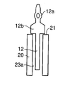
11 ハウジング(コネクタハウジングに相当する。)
12 端子(コネクタ端子に相当する。)
12a 弾性部
12b 鍔部
12c 曲げ部
12d 切欠部
12e 幅広部
12′ コネクタ端子材
20 コネクタ治具(治具に相当する。)
21 押し当て面(溝部の開放端の縁部に相当する。)
23 深溝(溝部に相当する。)
30 プリント基板(基板に相当する。)
32 貫通穴(穴部に相当する。)
Claims (2)
- 一方向に延び、その中間の特定部位が曲げ加工されてコネクタ端子を形成するコネクタ端子材であって、上記特定部位は、上記曲げ加工される方向と直交する端子幅方向の両端部に切欠部が形成されることによりこの特定部位に隣接する部分よりも幅狭とされた形状を有するコネクタ端子材を成形する工程と、
このコネクタ端子材を上記特定部位で曲げ加工することにより当該部位で屈曲したコネクタ端子を形成する工程とを含み、
上記コネクタ端子材を成形する工程は、
金属板を打ち抜き加工することにより、上記コネクタ端子材がその端子幅方向に複数個並びかつ各コネクタ端子材の上記特定部位同士が上記端子幅方向に延びるキャリア部を介して連結された形状の板材を成形する工程と、
その板材におけるキャリア部及びこのキャリア部の両側の上記切欠部に相当する部位を打ち抜くことにより、上記コネクタ端子材同士を分断すると同時にその分断したコネクタ端子材の特定部位に上記切欠部を形成する工程とを含むことを特徴とするコネクタ端子の製造方法。 - 請求項1記載のコネクタ端子の製造方法において、
上記コネクタ端子材の特定部位の幅は、この特定部位を最終角度まで曲げ加工したときにこの特定部位に隣接する部分と略同幅となるように設定されることを特徴とするコネクタ端子の製造方法。
Priority Applications (3)
| Application Number | Priority Date | Filing Date | Title |
|---|---|---|---|
| JP2004195101A JP4425730B2 (ja) | 2003-07-09 | 2004-07-01 | コネクタ端子の製造方法 |
| DE102004033103A DE102004033103B4 (de) | 2003-07-09 | 2004-07-08 | Verfahren zur Herstellung eines Steckeranschlusses, Steckeranschluss und Stecker mit Presspassung |
| US10/886,701 US7104811B2 (en) | 2003-07-09 | 2004-07-09 | Angled terminal with flange for cooperation with press-fit jig |
Applications Claiming Priority (2)
| Application Number | Priority Date | Filing Date | Title |
|---|---|---|---|
| JP2003194414 | 2003-07-09 | ||
| JP2004195101A JP4425730B2 (ja) | 2003-07-09 | 2004-07-01 | コネクタ端子の製造方法 |
Publications (2)
| Publication Number | Publication Date |
|---|---|
| JP2005044788A JP2005044788A (ja) | 2005-02-17 |
| JP4425730B2 true JP4425730B2 (ja) | 2010-03-03 |
Family
ID=34067324
Family Applications (1)
| Application Number | Title | Priority Date | Filing Date |
|---|---|---|---|
| JP2004195101A Expired - Fee Related JP4425730B2 (ja) | 2003-07-09 | 2004-07-01 | コネクタ端子の製造方法 |
Country Status (3)
| Country | Link |
|---|---|
| US (1) | US7104811B2 (ja) |
| JP (1) | JP4425730B2 (ja) |
| DE (1) | DE102004033103B4 (ja) |
Families Citing this family (19)
| Publication number | Priority date | Publication date | Assignee | Title |
|---|---|---|---|---|
| US20070117474A1 (en) * | 2005-11-21 | 2007-05-24 | Zippy Technology Corp. | Signal pin of switches |
| JP5157784B2 (ja) * | 2008-09-25 | 2013-03-06 | ミツミ電機株式会社 | 接続端子構成体、コネクタ、及びコネクタの組立方法 |
| DE102009025113A1 (de) * | 2009-06-11 | 2010-12-16 | Continental Teves Ag & Co. Ohg | Einpresskontakt zur Verbindung eines elektronischen Bauelementes mit einer Leiterplatte sowie Einpresswerkzeug |
| JP5140125B2 (ja) * | 2010-09-10 | 2013-02-06 | 矢崎総業株式会社 | コネクタ端子の製造方法およびコネクタ端子 |
| CN102610943B (zh) * | 2012-03-31 | 2014-02-26 | 上海沪工汽车电器有限公司 | 一种引出线弯角安装底板结构 |
| US10193292B2 (en) | 2012-11-30 | 2019-01-29 | J.S.T. Mfg. Co., Ltd. | Jig and press-fitting device comprising this jig |
| DE102014203248A1 (de) * | 2014-02-24 | 2015-08-27 | Robert Bosch Gmbh | Steckeranschlusselement, Verbindungsanordnung mit mehreren Steckeranschlusselementen in einem elektrischen Gerät und Einpresswerkzeug zur Ausbildung einer Verbindungsanordnung |
| TWM499687U (zh) * | 2014-07-28 | 2015-04-21 | Riidea Inc | 電連接器之結構改良 |
| JP6488688B2 (ja) * | 2014-12-17 | 2019-03-27 | ダイキン工業株式会社 | モジュール−端子台接続構造及び接続方法 |
| JP6485207B2 (ja) * | 2015-05-14 | 2019-03-20 | 富士通株式会社 | 圧入部材付きプレスフィットピン及びコネクタ |
| JP1640716S (ja) * | 2019-03-26 | 2019-09-09 | ||
| JP6883602B2 (ja) * | 2019-03-27 | 2021-06-09 | 矢崎総業株式会社 | コネクタ及びコネクタの製造方法 |
| JP7257900B2 (ja) * | 2019-07-06 | 2023-04-14 | 三晶エムイーシー株式会社 | コンタクト端子、電気コネクタ及びコンタクト端子の整列方法 |
| JP7435366B2 (ja) * | 2020-08-27 | 2024-02-21 | 住友電装株式会社 | 基板用コネクタ |
| CN112437557B (zh) * | 2020-12-01 | 2022-10-14 | 中国科学院长春光学精密机械与物理研究所 | 一种用于弯针连接器的辅助定位装置和弯针焊接方法 |
| CN114142322B (zh) * | 2021-11-17 | 2023-10-20 | 洛阳市鑫鼎源光电元件有限责任公司 | 一种连接器插针的弯曲设备 |
| US12218444B2 (en) * | 2022-08-12 | 2025-02-04 | Microsoft Technology Licensing, Llc | Assembly fixture for press-fitting contact pins in a printed circuit board assembly |
| USD1089124S1 (en) * | 2023-07-13 | 2025-08-19 | Chun-Jui Chen | Terminal |
| USD1089125S1 (en) * | 2023-08-31 | 2025-08-19 | Chun-Jui Chen | Terminal |
Family Cites Families (19)
| Publication number | Priority date | Publication date | Assignee | Title |
|---|---|---|---|---|
| US3742432A (en) * | 1972-04-24 | 1973-06-26 | Amp Inc | Electrical terminal having folded blade and method of manufacturing same |
| DE3318135A1 (de) * | 1983-05-18 | 1984-11-22 | Erni Elektroapparate Gmbh, 7321 Adelberg | Loetfreie elektrische verbindung |
| DE3327414C2 (de) * | 1983-07-29 | 1987-01-08 | Preh, Elektrofeinmechanische Werke Jakob Preh Nachf. Gmbh & Co, 8740 Bad Neustadt | Buchsenleiste |
| US4857019A (en) * | 1988-02-29 | 1989-08-15 | Molex Incorporated | Terminal pin with s-shaped complaint portion |
| US5080596A (en) * | 1990-11-30 | 1992-01-14 | Amp Incorporated | Connector with contact spacer plate providing greater lateral force on rear contacts |
| US5071372A (en) * | 1990-11-30 | 1991-12-10 | Amp Incorporated | Connector with contact spacer plate having tapered channels |
| JP3201047B2 (ja) * | 1993-01-28 | 2001-08-20 | 安藤電気株式会社 | プリント基板へのプレスフィットコネクタ圧入装置 |
| US5453016A (en) * | 1993-11-15 | 1995-09-26 | Berg Technology, Inc. | Right angle electrical connector and insertion tool therefor |
| EP0729653B1 (en) * | 1993-11-15 | 2001-05-16 | Berg Electronics Manufacturing B.V. | Right angle electrical connector and insertion tool |
| JP3650211B2 (ja) * | 1996-04-10 | 2005-05-18 | 富士通コンポーネント株式会社 | コネクタ |
| DE19621125C2 (de) * | 1996-05-24 | 1998-03-26 | Siemens Ag | Stiftsteckerteil für ein Stecksystem in SMD-Anschlußtechnik |
| US5848920A (en) * | 1996-07-16 | 1998-12-15 | Molex Incorporated | Fabrication of electrical terminals for edge card connectors |
| JP3106967B2 (ja) * | 1996-07-22 | 2000-11-06 | 住友電装株式会社 | 基板用コネクタ |
| JP3903572B2 (ja) * | 1998-02-09 | 2007-04-11 | 松下電器産業株式会社 | コネクタ端子およびそれを用いた回転スロットル位置センサ |
| DE29808731U1 (de) * | 1998-05-14 | 1999-09-23 | Robert Bosch Gmbh, 70469 Stuttgart | Kontaktschienen |
| DE10009215C1 (de) * | 2000-02-26 | 2001-05-10 | Harting Kgaa | Steckverbinder sowie Verfahren zur Herstellung eines Steckverbinders |
| JP2004031006A (ja) * | 2002-06-24 | 2004-01-29 | Sumitomo Wiring Syst Ltd | 端子の取付け構造及び回路基板用コネクタ |
| US6790054B1 (en) * | 2003-03-18 | 2004-09-14 | Sullins Electronic Corporation | Two-piece right angle contact edge card connector |
| JP2004319338A (ja) * | 2003-04-17 | 2004-11-11 | Sumitomo Wiring Syst Ltd | プレスフィット端子及び基板用コネクタ |
-
2004
- 2004-07-01 JP JP2004195101A patent/JP4425730B2/ja not_active Expired - Fee Related
- 2004-07-08 DE DE102004033103A patent/DE102004033103B4/de not_active Expired - Fee Related
- 2004-07-09 US US10/886,701 patent/US7104811B2/en not_active Expired - Fee Related
Also Published As
| Publication number | Publication date |
|---|---|
| JP2005044788A (ja) | 2005-02-17 |
| US7104811B2 (en) | 2006-09-12 |
| DE102004033103B4 (de) | 2008-04-17 |
| DE102004033103A1 (de) | 2005-02-10 |
| US20050014424A1 (en) | 2005-01-20 |
Similar Documents
| Publication | Publication Date | Title |
|---|---|---|
| JP4425730B2 (ja) | コネクタ端子の製造方法 | |
| JP3041845U (ja) | 電気端子 | |
| JP2803574B2 (ja) | コネクタのプレスイン端子及びその製造方法 | |
| US6379161B1 (en) | Method of making an electrical connector | |
| US20080050947A1 (en) | Double-ended press-fit connector | |
| US5133670A (en) | Surface mount connector with contact aligning member | |
| US10153568B2 (en) | Press-fit terminal and manufacturing method for same | |
| JP4839492B2 (ja) | コネクタの製造方法 | |
| JPH0679074U (ja) | コネクタ | |
| JPH11251004A (ja) | ターミナルが浮いた状態で配置されるコネクタ | |
| EP2073318A1 (en) | Terminal fitting insertion guide structure and electrical connector | |
| JP5578315B2 (ja) | 基板用端子 | |
| US6328585B1 (en) | Electrical connector having a contact element with large flexibility and a short transmission path | |
| JP2005228710A (ja) | プレスフィット端子およびプレスフィット端子の製造方法 | |
| KR20050035110A (ko) | 조인트 커넥터, 조인트 단자 및 조인트 단자 제조 방법 | |
| JP5157784B2 (ja) | 接続端子構成体、コネクタ、及びコネクタの組立方法 | |
| JP3929931B2 (ja) | コネクタの圧入用治具 | |
| JP2005302614A (ja) | コネクタとプリント基板との組付け構造および組付け方法 | |
| FI93594C (sv) | Kontaktelement | |
| US20220069504A1 (en) | Board connector | |
| JPH065324A (ja) | コネクタ | |
| JPH10264163A (ja) | インサート金型及びそれを用いた表面実装型コネクタ | |
| US6857894B2 (en) | Electrical connector having a contact and spring member | |
| CN222826654U (zh) | 电子插件及其压接端子 | |
| JP3880923B2 (ja) | プレスフィットコネクタとその製造方法 |
Legal Events
| Date | Code | Title | Description |
|---|---|---|---|
| A621 | Written request for application examination |
Free format text: JAPANESE INTERMEDIATE CODE: A621 Effective date: 20070622 |
|
| A977 | Report on retrieval |
Free format text: JAPANESE INTERMEDIATE CODE: A971007 Effective date: 20090810 |
|
| A131 | Notification of reasons for refusal |
Free format text: JAPANESE INTERMEDIATE CODE: A131 Effective date: 20090908 |
|
| A521 | Request for written amendment filed |
Free format text: JAPANESE INTERMEDIATE CODE: A523 Effective date: 20091014 |
|
| TRDD | Decision of grant or rejection written | ||
| A01 | Written decision to grant a patent or to grant a registration (utility model) |
Free format text: JAPANESE INTERMEDIATE CODE: A01 Effective date: 20091208 |
|
| A01 | Written decision to grant a patent or to grant a registration (utility model) |
Free format text: JAPANESE INTERMEDIATE CODE: A01 |
|
| A61 | First payment of annual fees (during grant procedure) |
Free format text: JAPANESE INTERMEDIATE CODE: A61 Effective date: 20091209 |
|
| R150 | Certificate of patent or registration of utility model |
Free format text: JAPANESE INTERMEDIATE CODE: R150 |
|
| FPAY | Renewal fee payment (event date is renewal date of database) |
Free format text: PAYMENT UNTIL: 20121218 Year of fee payment: 3 |
|
| FPAY | Renewal fee payment (event date is renewal date of database) |
Free format text: PAYMENT UNTIL: 20131218 Year of fee payment: 4 |
|
| R250 | Receipt of annual fees |
Free format text: JAPANESE INTERMEDIATE CODE: R250 |
|
| LAPS | Cancellation because of no payment of annual fees |