JP4352379B2 - Manufacturing method and manufacturing apparatus of organic electroluminescence element - Google Patents
Manufacturing method and manufacturing apparatus of organic electroluminescence element Download PDFInfo
- Publication number
- JP4352379B2 JP4352379B2 JP2003276524A JP2003276524A JP4352379B2 JP 4352379 B2 JP4352379 B2 JP 4352379B2 JP 2003276524 A JP2003276524 A JP 2003276524A JP 2003276524 A JP2003276524 A JP 2003276524A JP 4352379 B2 JP4352379 B2 JP 4352379B2
- Authority
- JP
- Japan
- Prior art keywords
- light emitting
- dye
- substrate
- emitting layer
- recesses
- Prior art date
- Legal status (The legal status is an assumption and is not a legal conclusion. Google has not performed a legal analysis and makes no representation as to the accuracy of the status listed.)
- Expired - Fee Related
Links
- 238000004519 manufacturing process Methods 0.000 title claims description 22
- 238000005401 electroluminescence Methods 0.000 title description 3
- 239000000758 substrate Substances 0.000 claims description 68
- 238000001704 evaporation Methods 0.000 claims description 9
- 238000010438 heat treatment Methods 0.000 claims description 6
- 239000000975 dye Substances 0.000 description 68
- 238000000034 method Methods 0.000 description 22
- 239000010408 film Substances 0.000 description 21
- 238000009792 diffusion process Methods 0.000 description 14
- 239000010409 thin film Substances 0.000 description 12
- 239000000463 material Substances 0.000 description 11
- 238000007740 vapor deposition Methods 0.000 description 9
- 229920002120 photoresistant polymer Polymers 0.000 description 7
- 239000002904 solvent Substances 0.000 description 6
- 238000001771 vacuum deposition Methods 0.000 description 6
- 230000008020 evaporation Effects 0.000 description 5
- 229910052741 iridium Inorganic materials 0.000 description 5
- GKOZUEZYRPOHIO-UHFFFAOYSA-N iridium atom Chemical compound [Ir] GKOZUEZYRPOHIO-UHFFFAOYSA-N 0.000 description 5
- 239000000243 solution Substances 0.000 description 5
- HEDRZPFGACZZDS-UHFFFAOYSA-N Chloroform Chemical compound ClC(Cl)Cl HEDRZPFGACZZDS-UHFFFAOYSA-N 0.000 description 4
- 238000005192 partition Methods 0.000 description 4
- 229920003227 poly(N-vinyl carbazole) Polymers 0.000 description 4
- 230000001681 protective effect Effects 0.000 description 4
- -1 4-biphenylyl Chemical group 0.000 description 3
- YXFVVABEGXRONW-UHFFFAOYSA-N Toluene Chemical compound CC1=CC=CC=C1 YXFVVABEGXRONW-UHFFFAOYSA-N 0.000 description 3
- 239000003086 colorant Substances 0.000 description 3
- 239000000049 pigment Substances 0.000 description 3
- 230000007261 regionalization Effects 0.000 description 3
- 238000004804 winding Methods 0.000 description 3
- FQJQNLKWTRGIEB-UHFFFAOYSA-N 2-(4-tert-butylphenyl)-5-[3-[5-(4-tert-butylphenyl)-1,3,4-oxadiazol-2-yl]phenyl]-1,3,4-oxadiazole Chemical compound C1=CC(C(C)(C)C)=CC=C1C1=NN=C(C=2C=C(C=CC=2)C=2OC(=NN=2)C=2C=CC(=CC=2)C(C)(C)C)O1 FQJQNLKWTRGIEB-UHFFFAOYSA-N 0.000 description 2
- CFNMUZCFSDMZPQ-GHXNOFRVSA-N 7-[(z)-3-methyl-4-(4-methyl-5-oxo-2h-furan-2-yl)but-2-enoxy]chromen-2-one Chemical compound C=1C=C2C=CC(=O)OC2=CC=1OC/C=C(/C)CC1OC(=O)C(C)=C1 CFNMUZCFSDMZPQ-GHXNOFRVSA-N 0.000 description 2
- 229920001609 Poly(3,4-ethylenedioxythiophene) Polymers 0.000 description 2
- 230000015572 biosynthetic process Effects 0.000 description 2
- 230000007423 decrease Effects 0.000 description 2
- 238000005530 etching Methods 0.000 description 2
- 230000005525 hole transport Effects 0.000 description 2
- 238000002347 injection Methods 0.000 description 2
- 239000007924 injection Substances 0.000 description 2
- 238000004020 luminiscence type Methods 0.000 description 2
- UHOVQNZJYSORNB-UHFFFAOYSA-N monobenzene Natural products C1=CC=CC=C1 UHOVQNZJYSORNB-UHFFFAOYSA-N 0.000 description 2
- 238000000206 photolithography Methods 0.000 description 2
- BASFCYQUMIYNBI-UHFFFAOYSA-N platinum Chemical compound [Pt] BASFCYQUMIYNBI-UHFFFAOYSA-N 0.000 description 2
- 238000004544 sputter deposition Methods 0.000 description 2
- XLYOFNOQVPJJNP-UHFFFAOYSA-N water Substances O XLYOFNOQVPJJNP-UHFFFAOYSA-N 0.000 description 2
- POILWHVDKZOXJZ-ARJAWSKDSA-M (z)-4-oxopent-2-en-2-olate Chemical compound C\C([O-])=C\C(C)=O POILWHVDKZOXJZ-ARJAWSKDSA-M 0.000 description 1
- KLCLIOISYBHYDZ-UHFFFAOYSA-N 1,4,4-triphenylbuta-1,3-dienylbenzene Chemical compound C=1C=CC=CC=1C(C=1C=CC=CC=1)=CC=C(C=1C=CC=CC=1)C1=CC=CC=C1 KLCLIOISYBHYDZ-UHFFFAOYSA-N 0.000 description 1
- OCJBOOLMMGQPQU-UHFFFAOYSA-N 1,4-dichlorobenzene Chemical compound ClC1=CC=C(Cl)C=C1 OCJBOOLMMGQPQU-UHFFFAOYSA-N 0.000 description 1
- CRGSMSNUTNRNQM-UHFFFAOYSA-N 2-(4-tert-butylphenyl)-1,3,4-oxadiazole Chemical compound C1=CC(C(C)(C)C)=CC=C1C1=NN=CO1 CRGSMSNUTNRNQM-UHFFFAOYSA-N 0.000 description 1
- YLYPIBBGWLKELC-RMKNXTFCSA-N 2-[2-[(e)-2-[4-(dimethylamino)phenyl]ethenyl]-6-methylpyran-4-ylidene]propanedinitrile Chemical compound C1=CC(N(C)C)=CC=C1\C=C\C1=CC(=C(C#N)C#N)C=C(C)O1 YLYPIBBGWLKELC-RMKNXTFCSA-N 0.000 description 1
- ZOKXTWBITQBERF-UHFFFAOYSA-N Molybdenum Chemical compound [Mo] ZOKXTWBITQBERF-UHFFFAOYSA-N 0.000 description 1
- 239000004695 Polyether sulfone Substances 0.000 description 1
- 239000004642 Polyimide Substances 0.000 description 1
- NRCMAYZCPIVABH-UHFFFAOYSA-N Quinacridone Chemical class N1C2=CC=CC=C2C(=O)C2=C1C=C1C(=O)C3=CC=CC=C3NC1=C2 NRCMAYZCPIVABH-UHFFFAOYSA-N 0.000 description 1
- 229910052581 Si3N4 Inorganic materials 0.000 description 1
- 229910004298 SiO 2 Inorganic materials 0.000 description 1
- 235000005811 Viola adunca Nutrition 0.000 description 1
- 240000009038 Viola odorata Species 0.000 description 1
- 235000013487 Viola odorata Nutrition 0.000 description 1
- 235000002254 Viola papilionacea Nutrition 0.000 description 1
- NLESIEMIRNKQEI-UHFFFAOYSA-N [Ir]c1cccnc1-c1ccccc1 Chemical compound [Ir]c1cccnc1-c1ccccc1 NLESIEMIRNKQEI-UHFFFAOYSA-N 0.000 description 1
- CUJRVFIICFDLGR-UHFFFAOYSA-N acetylacetonate Chemical compound CC(=O)[CH-]C(C)=O CUJRVFIICFDLGR-UHFFFAOYSA-N 0.000 description 1
- 150000004035 chlorins Chemical class 0.000 description 1
- 239000011248 coating agent Substances 0.000 description 1
- 238000000576 coating method Methods 0.000 description 1
- AFYCEAFSNDLKSX-UHFFFAOYSA-N coumarin 460 Chemical compound CC1=CC(=O)OC2=CC(N(CC)CC)=CC=C21 AFYCEAFSNDLKSX-UHFFFAOYSA-N 0.000 description 1
- VBVAVBCYMYWNOU-UHFFFAOYSA-N coumarin 6 Chemical compound C1=CC=C2SC(C3=CC4=CC=C(C=C4OC3=O)N(CC)CC)=NC2=C1 VBVAVBCYMYWNOU-UHFFFAOYSA-N 0.000 description 1
- 238000010586 diagram Methods 0.000 description 1
- 229940117389 dichlorobenzene Drugs 0.000 description 1
- AMGQUBHHOARCQH-UHFFFAOYSA-N indium;oxotin Chemical compound [In].[Sn]=O AMGQUBHHOARCQH-UHFFFAOYSA-N 0.000 description 1
- 238000010884 ion-beam technique Methods 0.000 description 1
- 238000003801 milling Methods 0.000 description 1
- 229910052750 molybdenum Inorganic materials 0.000 description 1
- 239000011733 molybdenum Substances 0.000 description 1
- 229910052757 nitrogen Inorganic materials 0.000 description 1
- 239000012299 nitrogen atmosphere Substances 0.000 description 1
- 230000003287 optical effect Effects 0.000 description 1
- 239000011368 organic material Substances 0.000 description 1
- 239000003960 organic solvent Substances 0.000 description 1
- 150000004880 oxines Chemical class 0.000 description 1
- 125000002080 perylenyl group Chemical group C1(=CC=C2C=CC=C3C4=CC=CC5=CC=CC(C1=C23)=C45)* 0.000 description 1
- CSHWQDPOILHKBI-UHFFFAOYSA-N peryrene Natural products C1=CC(C2=CC=CC=3C2=C2C=CC=3)=C3C2=CC=CC3=C1 CSHWQDPOILHKBI-UHFFFAOYSA-N 0.000 description 1
- 229910052697 platinum Inorganic materials 0.000 description 1
- 229920006393 polyether sulfone Polymers 0.000 description 1
- 229920001721 polyimide Polymers 0.000 description 1
- 239000002861 polymer material Substances 0.000 description 1
- 150000004033 porphyrin derivatives Chemical class 0.000 description 1
- 239000000843 powder Substances 0.000 description 1
- HQVNEWCFYHHQES-UHFFFAOYSA-N silicon nitride Chemical compound N12[Si]34N5[Si]62N3[Si]51N64 HQVNEWCFYHHQES-UHFFFAOYSA-N 0.000 description 1
- 239000000126 substance Substances 0.000 description 1
- WFKWXMTUELFFGS-UHFFFAOYSA-N tungsten Chemical compound [W] WFKWXMTUELFFGS-UHFFFAOYSA-N 0.000 description 1
- 229910052721 tungsten Inorganic materials 0.000 description 1
- 239000010937 tungsten Substances 0.000 description 1
- 238000001039 wet etching Methods 0.000 description 1
Images


Landscapes
- Electroluminescent Light Sources (AREA)
Description
本発明は、有機エレクトロルミネセンス(有機EL)素子の製造方法及び製造装置に関する。 The present invention relates to a manufacturing method and a manufacturing apparatus of an organic electroluminescence (organic EL) element.
一般的に、nm〜μmオーダーの薄膜を形成するとき、真空蒸着法が用いられている。図16は一般的な蒸着法を示す蒸着機装置の断面図である。51は真空槽である。真空槽51の中に加熱源のボート52が配置されている。ボート52略中央の凹部に蒸発材料53が粉末、バルクなどの形態で配置される。ボート52の上方に基板54が、ボート52に対向して配置されている。そして、真空槽51内部を排気して、真空にする。ボート52は通常タングステンやモリブデンなどの抵抗体からなり、電流を流し発熱させる。ボート52の発熱により、蒸発材料53が加熱され、蒸発材料53は真空槽51中の基板54の方向に蒸発する。基板54表面に、蒸発した蒸発材料53が飛来し、堆積して、一様な厚みの薄膜となる。以上が一般的な抵抗加熱型真空蒸着法である。
Generally, when forming a thin film of the order of nm to μm, a vacuum deposition method is used. FIG. 16 is a cross-sectional view of a vapor deposition apparatus showing a general vapor deposition method. 51 is a vacuum chamber. A
図17は一般的なフォトレジストによる薄膜パターンの形成法を基板断面図で示したものである。前記の基板54表面に、前記蒸発材料53よりなる前記一様な厚みの薄膜55が形成されている。この薄膜55上にフォトレジスト56を基板スピンにより塗布する。一様に塗布されたフォトレジスト56を希望のパターン形状の光パターンによって露光、現像を行い、レジストパターン形状を作製する。基板54上の薄膜55は、フォトレジスト56によって被覆された部分と、露出した除去すべき部分がある。RIE、イオンビームミリング、ウェットエッチング法などのエッチング手段で、露出した除去すべき部分を取り除き、最後にフォトレジスト56を有機などの溶剤で溶かして除去し、希望の薄膜パターンを得る。以上が一般的なフォトレジストによる薄膜パターン形成の方法(フォトリソグラフィーパターン形成法)である。
FIG. 17 is a cross-sectional view of a substrate showing a method for forming a thin film pattern using a general photoresist. The uniform
これら図17のような一般的なフォトリソグラフィーパターン形成法が適用できる薄膜材料は、耐水性、耐溶剤性を備えている必要がある。そのため、有機EL素子に用いられる材料のように耐水性、耐溶剤性の低いものを薄膜パターン形成する場合には、真空マスク蒸着法等で行うのが一般的である。 A thin film material to which a general photolithography pattern forming method as shown in FIG. 17 can be applied needs to have water resistance and solvent resistance. Therefore, when a thin film pattern is formed of a material having low water resistance and low solvent resistance, such as a material used for an organic EL element, it is generally performed by a vacuum mask vapor deposition method or the like.
例えば特開平10−321372号公報(特許文献1)に開示されているパターン形成方法(真空マスク蒸着法)は、複数の発光部を有する有機ELディスプレイパネルとその製造方法に関するものである。特許文献1記載の有機ELディスプレイパネルは、基板と、基板の一面側に形成された複数の第一電極と、第一電極の一部分を露出させかつ、他部分を覆うように基板の一面から突出して形成された複数の電気絶縁性の隔壁と、第一電極の露出部分の各々の上に形成された有機EL媒体の層と、有機EL媒体の層上に形成された複数の第二電極とを備え、隔壁の突出上部に凹部を形成するものである。 For example, a pattern formation method (vacuum mask vapor deposition method) disclosed in Japanese Patent Laid-Open No. 10-321372 (Patent Document 1) relates to an organic EL display panel having a plurality of light emitting portions and a method for manufacturing the same. The organic EL display panel described in Patent Document 1 protrudes from one surface of the substrate so as to expose the substrate, the plurality of first electrodes formed on one surface side of the substrate, and a portion of the first electrode, and to cover the other portion. A plurality of electrically insulating partition walls formed on the exposed portion of the first electrode, an organic EL medium layer formed on each of the exposed portions of the first electrode, and a plurality of second electrodes formed on the organic EL medium layer. And a recess is formed in the protruding upper portion of the partition wall.
また、特許文献1記載の有機ELディスプレイパネルの製造方法は、発光層形成工程において、露出した第一電極のうち、所望の部分のみを露出する複数の開口を有するマスクを隔壁の突出上部に載置し、所定の色の有機発光層を開口を通じて堆積させ、その後、開口が有機発光層の堆積されていない部分を露出するようにマスクを移動させ同様の工程を行うことを各色で繰り返し、その後、全面に陰極層を成膜するものである。
フルカラーの有機EL素子においては、赤、緑、青色発光の微細な素子(ピクセル)を組み合わせて1つの画素とする必要がある。しかし、特許文献1におけるパターン形成方法では、数10μm程度のパターン形成が限界である。これは、マスクにパターンを形成する際に、そのパターンが細かくなるのに応じてマスクの厚みを薄くする必要があるからである。マスクの厚みが薄くなるとマスクにたわみが生じ、基板との間に隙間が生じる。その隙間によって色素がマスクのパターンよりも広い範囲に広がるために、色素がにじみ、ぼけてしまうのである。 In a full-color organic EL element, it is necessary to combine fine elements (pixels) emitting red, green, and blue to form one pixel. However, the pattern formation method in Patent Document 1 has a limit of pattern formation of about several tens of μm. This is because when the pattern is formed on the mask, it is necessary to reduce the thickness of the mask as the pattern becomes finer. When the thickness of the mask is reduced, the mask is bent and a gap is formed between the mask and the substrate. The pigment spreads over a wider range than the mask pattern due to the gap, and the pigment is blurred and blurred.
また、各色発光層を塗り分ける際、それぞれシャドウマスクの位置合わせ及び蒸着源の切り替えをしなければならず、手間がかかる。
そこで本発明では、高精細で、製造工程を簡略化することができる有機EL素子の製造方法及び製造装置を提供することを目的とする。
Moreover, when coating each color light emitting layer separately, it is necessary to perform alignment of the shadow mask and switching of the vapor deposition source, which is troublesome.
Therefore, an object of the present invention is to provide a manufacturing method and a manufacturing apparatus of an organic EL element that can simplify the manufacturing process with high definition.
本発明は、上述した従来の技術の課題を解決するため、以下の(a)、(b)の有機EL素子の製造方法及び製造装置を提供するものである。 In order to solve the above-described problems of the related art, the present invention provides the following methods (a) and (b) for manufacturing an organic EL element and a manufacturing apparatus.
(a)少なくとも、複数の第一の電極(11)と、青色発光色素(14B)が分散された発光層(13)とが形成された第一の基板(10)に対し、前記第一の電極の配列に対応した複数の凹部(22)と前記複数の凹部それぞれに貫通孔(23)が形成された第二の基板(21)を、前記第一の電極と前記凹部とが対応するように対向させて前記発光層と前記第二の基板の前記凹部が形成された面とが接するように配置する工程と、前記複数の凹部に前記貫通孔を通じて赤色発光色素(14R)または緑色発光色素(14G)が充填する色素充填工程と、前記赤色発光色素及び前記緑色発光色素を加熱して蒸発させ、前記赤色発光色素及び前記緑色発光色素を前記第一の基板の前記発光層内に拡散させる工程と、前記発光層内に前記赤色発光色素及び前記緑色発光色素が拡散した前記第一の基板に、第二の電極(15)を形成する工程とを含むことを特徴とする有機エレクトロルミネセンス素子の製造方法。 (A) For the first substrate (10) formed with at least a plurality of first electrodes (11) and a light emitting layer (13) in which a blue light emitting dye (14B) is dispersed, A plurality of recesses (22) corresponding to the arrangement of the electrodes and a second substrate (21) in which through holes (23) are formed in each of the plurality of recesses , the first electrode and the recesses correspond to each other. A step of disposing the light emitting layer so as to be in contact with the surface of the second substrate on which the concave portion is formed, and a red light emitting dye (14R) or a green light emitting dye through the through holes in the plurality of concave portions. (14G) is filled with a dye filling step, and the red light emitting dye and the green light emitting dye are heated and evaporated to diffuse the red light emitting dye and the green light emitting dye into the light emitting layer of the first substrate. And the red light emission in the light emitting layer. On the first substrate to the dye and the green luminescent dye has diffused, the method of manufacturing the organic electroluminescent element which comprises a step of forming a second electrode (15).
(b)少なくとも、複数の第一の電極(11)と、青色発光色素(14B)が分散された発光層(13)とが形成された第一の基板(10)と、前記第一の電極の配列に対応した複数の凹部(22)と、前記複数の凹部それぞれに貫通孔(23)を有する第二の基板(21)と、前記第二の基板の前記複数の凹部が、前記第一の基板における前記第一の電極に対応するように対向させて前記発光層と前記第二の基板の前記凹部が形成された面とが接するように配置するための配置手段と、前記凹部に前記貫通孔を通じて赤色発光色素(14R)または緑色発光色素(14G)を充填するための色素充填手段と、前記赤色発光色素及び前記緑色発光色素を加熱して蒸発させ、前記赤色発光色素及び前記緑色発光色素を前記第一の基板の前記発光層内に拡散させるための色素拡散手段と、前記発光層内に前記赤色発光色素及び前記緑色発光色素が拡散した前記第一の基板に、第二の電極(15)を形成する成膜手段と、前記第一の基板を前記配置手段から前記成膜手段へと搬送するための基板搬送手段(1)とを備えたことを特徴とする有機エレクトロルミネセンス素子の製造装置。
(B) a first substrate (10) on which at least a plurality of first electrodes (11) and a light emitting layer (13) in which a blue light emitting dye (14B) is dispersed are formed , and the first electrode A plurality of recesses (22) corresponding to the arrangement of the second substrate (21) having a through hole (23) in each of the plurality of recesses, and the plurality of recesses of the second substrate. and placement means for by opposing arranged such that the recess is formed a surface of the second substrate and the light emitting layer is in contact with so as to correspond to the first electrode in the substrate, the said recess Dye filling means for filling the red light emitting dye (14R) or the green light emitting dye (14G) through the through hole, and heating and evaporating the red light emitting dye and the green light emitting dye, and the red light emitting dye and the green light emitting The light emission of the first substrate A dye diffusing means for diffusing in, and a film forming means for forming a second electrode (15) on the first substrate in which the red luminescent dye and the green luminescent dye are diffused in the light emitting layer; An apparatus for manufacturing an organic electroluminescence element, comprising: a substrate transfer means (1) for transferring the first substrate from the arrangement means to the film forming means.
本発明の製造方法は、高精細の有機EL素子を製造でき、製造工程を簡略化することができる。 The production method of the present invention can produce a high-definition organic EL element and can simplify the production process.
以下、本発明の一実施形態である有機EL素子の製造方法について、添付図面を参照して説明する。図1は装置全体の模式図である。大きく分けて、シート基板10の供給部としての供給ロール2、巻取り部としての巻取りロール3よりなるシート基板搬送系1と、スタンプ21、ヒータ25からなる発光色素拡散系20と、蒸着、スパッタを行なう真空成膜系30、31とより構成されている。
Hereinafter, the manufacturing method of the organic EL element which is one Embodiment of this invention is demonstrated with reference to an accompanying drawing. FIG. 1 is a schematic diagram of the entire apparatus. Broadly speaking, a sheet substrate transport system 1 including a
図2に示すように、シート基板としては、例えば、ポリエーテルサルフォン、ポリイミド等を用いたシート上に、TFT(Thin Film Transistor)(図示せず)が形成されたシートTFT基板10を用いることができる。画素電極(陽極)11としては、本実施形態では、仕事関数が高く透明なITO(Indium Tin Oxide)を用いて、一辺13μmの正方形のものをシートTFT基板10上に1μmおきに並べた。そして、図3に示すように、その上に正孔輸送層12であるPEDOT/PSS(ポリ(3,4−エチレンジオキシチオフェン))を50nm程度、さらに発光層13を80nm程度、印刷法等により成膜した。
As shown in FIG. 2, as the sheet substrate, for example, a
発光層13は、成膜の容易性、膜の熱的性質の安定性や機械的安定性などを考えれば高分子材料が最適であり、例えば青紫色に発光するポリビニルカルバゾール(PVK)があげられる。これに青色発光色素14Bを分散しておく。青色発光色素14Bとしてはクマリン47などのクマリン誘導体、テトラフェニルブタジエン、ペリレン、三重項励起子発光をするイリジウム錯体などを用いることができる。本実施形態では、高効率に発光するイリジウム錯体であるFIrpicを用い、これをPVKに10wt%分散した。またPVKは電子輸送性に乏しいので、OXD−7({1,3−ビス(4−tert−ブチルフェニル−1,3,4−オキサジアゾール)−2−イル}ベンゼン)、PBD(2−(4−ビフェニリル)―5−(4−tert−ブチフェニル)−1,3,4−オキサジアゾール)等の電子輸送性材料を分散させておくことが望ましい。本実施形態では、OXD−7を30wt%分散した。
The light-emitting
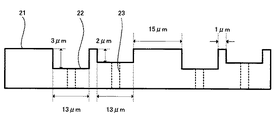
図4(a)、図5に示すように、スタンプ21は、微細加工の出来るSi等を用いた基板の表面にフォトリソグラフィー法、エッチング法等の方法により、凹部22よりなるストライプパターンを形成し、各凹部22に一カ所貫通孔23を設けたものである。このスタンプ21は図4(b)に示すようなドラム形状も考えられる。
As shown in FIGS. 4A and 5, the
シートTFT基板10を用いて、赤、緑、青の発光がそれぞれ13μmの幅で1μmおきに得られるようにするには、図5に示すようにスタンプ21のストライプパターンの凹部22の幅を13μm、凸部の幅を交互に1μm、15μmとする。これは、前述のように発光層13に青色発光色素14Bが分散されており、後述のように発光層13に赤色発光色素14Rと緑色発光色素14Gとを拡散させるからである。
In order to obtain red, green, and blue light emission with a width of 13 μm every 1 μm using the
同じ拡散条件における発光色素の拡散量は、凹部の深さが小さいほど増加し、大きいほど減少する。各色の発光色素の蒸発温度が異なる組み合わせとなる場合は、各色の凹部の深さを変えて、各色の最適拡散条件を揃える必要がある。本実施形態では赤色発光色素14RとしてBtp2Ir(acac)(ビス[2−(2‘ベンゾシエニル)−ピリジネイト−N,C3](アセチルアセトネイト)イリジウム錯体)、緑色発光色素14GとしてIr(ppy)3(fac−トリ(2−フェニルピリジル)イリジウム錯体)を用い、赤色発光色素14R凹部の深さは2μm、緑色発光色素14G凹部の深さは3μmとした。この深さは実験的に決定した。
The diffusion amount of the luminescent dye under the same diffusion condition increases as the depth of the concave portion decreases, and decreases as it increases. When the evaporation temperatures of the luminescent dyes of the respective colors are different from each other, it is necessary to change the depth of the concave portions of the respective colors to align the optimum diffusion conditions for the respective colors. In the present embodiment, Btp 2 Ir (acac) (bis [2- (2′benzocyenyl) -pyridinate-N, C 3 ] (acetylacetonate) iridium complex) is used as the red light-emitting
図6に示すように、貫通孔23は各色毎につながり、その先は各色色素溶液容器24R、24Gにつながっている。各色色素溶液容器24R、24Gからスタンプ21の凹部22に、クロロホルム、トルエン、ジクロロベンゼン等の有機溶剤に発光色素を1wt%〜数十wt%程度溶解した各色溶液14Rs、14Gsを供給する。そして、色素が蒸発しない100℃程度の温度で溶媒を蒸発させ数nm〜数百nm程度成膜する。本実施形態においては、溶媒としてクロロホルムを用いた30wt%の色素溶液を凹部溝底から1μmの高さまで充填し、溶媒を蒸発させ、300nmの成膜を行なった。なお、貫通孔23がつながるのはスタンプ21内でもよい。
As shown in FIG. 6, the through
発光色素としては、上記した本実施形態で用いたもの以外に、赤色発光色素14Rとしてはニールレッド、DCM1などのピラン誘導体、スクアリリウム誘導体、ポルフィリン誘導体、クロリン誘導体、ユーロジリン誘導体、三重項励起子発光をするイリジウム錯体やプラチナ錯体等を用いることもできる。同様に、緑色発光色素14Gとしてはクマリン6などのクマリン誘導体、キナクリドン誘導体、三重項励起子発光をするイリジウム錯体等を用いることもできる。ここで、各色発光色素を成膜する順番は特に制限するものではない。
As the luminescent dye, in addition to those used in the present embodiment, neil red, pyran derivatives such as DCM1, squarylium derivatives, porphyrin derivatives, chlorin derivatives, eurodillin derivatives, triplet exciton luminescence are used as the red
図7に示すようにシートTFT基板10を窒素雰囲気中の(望ましくは露点−50℃以下)、スタンプ21と対向した所定の位置に搬送し、陽極11の各列をスタンプ21の凹部22と対向させ載置する。そして、図8に示すように、シートTFT基板10とスタンプ21とを接触(密着)させる。
As shown in FIG. 7, the
このとき、スタンプ21の表面は直接発光層13に接するのみで、凹部の各発光色素14R、14Gが発光層13に直接触れることはない。また、図7,8,13におけるスタンプ21とシートTFT基板10との関係は、図1とは上下関係を逆にして図示している。なお、スタンプ21とシートTFT基板10の上下関係の配置は図1に限定されるものではない。
At this time, the surface of the
図8に示すように、スタンプ21内のヒータ25を用いて所定の温度で所定の時間加熱すると、各色発光色素14R、14Gは蒸発し、発光層13に到達した後、その位置で発光層13中に拡散(ドープ)する。本実施形態では、加熱温度、時間はそれぞれ180℃、5分とした。先に示したスタンプ21の各色凹部の深さ(2μm、3μm)は各色でこの拡散条件が最適になるように調節した結果である。
As shown in FIG. 8, when the
本発明において、各色発光色素14R、14Gは青色発光色素14Bを分散した発光層13中に拡散する。発光層13中における14R、14G各色の発光色素濃度には、適当な値があり、それ以下であるとその発光色素の発光が得られず、それ以上では濃度消光により発光効率が落ちてしまう。しかしながら、14R、14G各色の発光色素濃度が適切であれば、波長の短い青色発光色素14Bから、波長の長い赤色発光色素14R、緑色発光色素14Gへエネルギーの移動が起こる。従って赤色発光色素14R、緑色発光色素14Gの拡散された部分では青色発光色素14Bの発光が起こることがなく、各色の発光が適切に得られる。本実施形態において、発光を得るための充分な発光色素濃度は1wt%程度であった。
In the present invention, each color
その後、図9に示すようにシートTFT基板10を矢印A方向に搬送して、真空蒸着成膜槽30に送る一方で、連なったシートTFT基板10の色素拡散工程未処理部分が、発光色素拡散系20のスタンプ21上に送られてきて、その部分では前記の色素拡散の工程が行われる。同時に、真空蒸着成膜槽30では、送られたシートTFT基板10の発光層13上の所定の位置に、仕事関数が低く、図10に図示する陰極15の材料に適した物質15a、例えばMg0.9Ag0.1などを真空蒸着により、100nm程度形成する。
After that, as shown in FIG. 9, the
その後、シートTFT基板10の陰極成膜部分は真空スパッタ成膜槽31に送られ、真空スパッタ成膜槽31では窒化シリコンなどの耐湿保護材料16aを用いて、所定の厚さ、例えば1μm程度の図10に図示する耐湿保護膜16を形成する。一方、連なったシートTFT基板10の色素拡散処理部分は発光色素拡散系20から真空蒸着成膜槽30に送られ、前記の陰極成膜の工程が行われる。さらに連なったシートTFT基板10の色素拡散未処理部分はスタンプ21上に送られ、その部分では前記の色素拡散の工程が行われる。
Thereafter, the cathode film forming portion of the
これらの工程(色素拡散工程、陰極成膜工程、保護膜成膜工程)が順に行われることにより、有機EL素子が順に作製できる。作製した部分はロール状に巻かれる。以上のように作成された有機EL素子は、所望の大きさに切り取られて使用される。 By performing these steps (a dye diffusion step, a cathode film forming step, and a protective film forming step) in order, an organic EL element can be manufactured in order. The produced part is wound into a roll. The organic EL element produced as described above is cut into a desired size and used.
図10に示すように有機EL素子は任意の陽極11と陰極15との間に電圧を印加することにより、任意のピクセルの発光をシートTFT基板10の下面から取り出すことができる。また、図11のように耐湿保護膜以外の膜構成を図10とは逆にして作製することも可能で、その場合はシートTFT基板10の上面から光を取り出すことになる。このような場合は不透明なシートTFT基板を用いることもできる。
As shown in FIG. 10, the organic EL element can take out light emission of an arbitrary pixel from the lower surface of the
このほか、図12に示すように、正孔注入層17を陽極11と正孔輸送層12との間に形成し、電子注入層18、電子輸送層19を発光層13と陰極15との間に形成することにより発光効率を向上させることも可能である。また、図13に示すように、予めシートTFT基板10上に並べられた陽極11の間にSiO2などの隔壁101をスパッタ法などにより形成しておいて、スタンプ21をシートTFT基板10の発光層13上に載置する際、スタンプ21の表面が直接発光層13に接触しないようにすることも可能である。
In addition, as shown in FIG. 12, a
なお、スタンプ21は図14に示すように、真空槽26内に設置しておくことも可能である。この場合はシートTFT基板10をまず真空槽26内に搬送し、陽極11の各列をスタンプ21の凹部22と対向させ載置する。また、図15に示すようにシートTFT基板10全体を予め真空槽4、5内に載置しておき、シートTFT基板10をスタンプ21と対向した所定の位置に搬送し、陽極11の各列をスタンプ21の凹部22と対向させ載置することも可能である。
The
1 シート基板輸送系
2 供給ロール
3 巻取りロール
10 シート基板
11 画素電極(陽極)
13 発光層
14R 赤色発光色素
14G 緑色発光色素
14B 青色発光色素
15 陰極
20 色素拡散系
21 スタンプ
22 凹部
25 ヒータ
30 真空蒸着成膜槽
31 真空スパッタ成膜槽
DESCRIPTION OF SYMBOLS 1 Sheet
13
Claims (2)
前記複数の凹部に前記貫通孔を通じて赤色発光色素または緑色発光色素を充填する色素充填工程と、
前記赤色発光色素及び前記緑色発光色素を加熱して蒸発させ、前記赤色発光色素及び前記緑色発光色素を前記第一の基板の前記発光層内に拡散させる工程と、
前記発光層内に前記赤色発光色素及び前記緑色発光色素が拡散した前記第一の基板に、第二の電極を形成する工程と
を含むことを特徴とする有機エレクトロルミネセンス素子の製造方法。 Even without small, a plurality of first electrode with respect to the first substrate and the light emitting layer is formed of a blue emitting dye is dispersed, a plurality of recesses and the plurality of corresponding to the arrangement of the first electrode A surface of the light emitting layer and the second substrate on which the concave portion is formed with a second substrate having a through hole formed in each of the concave portions so that the first electrode and the concave portion correspond to each other ; placing such contacts,
A dye filling step of filling the plurality of recesses with a red light emitting dye or a green light emitting dye through the through hole; and
Heating and evaporating the red light emitting dye and the green light emitting dye, and diffusing the red light emitting dye and the green light emitting dye into the light emitting layer of the first substrate;
Forming a second electrode on the first substrate in which the red light emitting dye and the green light emitting dye are diffused in the light emitting layer. A method for producing an organic electroluminescent element, comprising:
前記第一の電極の配列に対応した複数の凹部と、前記複数の凹部それぞれに貫通孔を有する第二の基板と、
前記第二の基板の前記複数の凹部が、前記第一の基板における前記第一の電極に対応するように対向させて前記発光層と前記第二の基板の前記凹部が形成された面とが接するように配置するための配置手段と、
前記凹部に前記貫通孔を通じて赤色発光色素または緑色発光色素を充填するための色素充填手段と、
前記赤色発光色素及び前記緑色発光色素を加熱して蒸発させ、前記赤色発光色素及び前記緑色発光色素を前記第一の基板の前記発光層内に拡散させるための色素拡散手段と、
前記発光層内に前記赤色発光色素及び前記緑色発光色素が拡散した前記第一の基板に、第二の電極を形成する成膜手段と、
前記第一の基板を前記配置手段から前記成膜手段へと搬送するための基板搬送手段と
を備えることを特徴とする有機エレクトロルミネセンス素子の製造装置。 Even without small, a plurality of first electrodes, a first substrate and a light emitting layer is formed of a blue emitting dye is dispersed,
A plurality of recesses corresponding to the arrangement of the first electrodes, a second substrate having a through hole in each of the plurality of recesses,
The plurality of recesses of the second substrate are opposed to correspond to the first electrode of the first substrate, and the light emitting layer and the surface of the second substrate on which the recesses are formed An arrangement means for arranging to contact ,
A dye filling means for filling the concave portion with a red light emitting dye or a green light emitting dye through the through hole ;
A dye diffusing means for heating and evaporating the red luminescent dye and the green luminescent dye, and diffusing the red luminescent dye and the green luminescent dye into the light emitting layer of the first substrate;
A film forming means for forming a second electrode on the first substrate in which the red light emitting dye and the green light emitting dye are diffused in the light emitting layer;
An apparatus for manufacturing an organic electroluminescent element, comprising: a substrate transfer means for transferring the first substrate from the placement means to the film forming means.
Priority Applications (1)
| Application Number | Priority Date | Filing Date | Title |
|---|---|---|---|
| JP2003276524A JP4352379B2 (en) | 2003-07-18 | 2003-07-18 | Manufacturing method and manufacturing apparatus of organic electroluminescence element |
Applications Claiming Priority (1)
| Application Number | Priority Date | Filing Date | Title |
|---|---|---|---|
| JP2003276524A JP4352379B2 (en) | 2003-07-18 | 2003-07-18 | Manufacturing method and manufacturing apparatus of organic electroluminescence element |
Publications (2)
| Publication Number | Publication Date |
|---|---|
| JP2005038784A JP2005038784A (en) | 2005-02-10 |
| JP4352379B2 true JP4352379B2 (en) | 2009-10-28 |
Family
ID=34212820
Family Applications (1)
| Application Number | Title | Priority Date | Filing Date |
|---|---|---|---|
| JP2003276524A Expired - Fee Related JP4352379B2 (en) | 2003-07-18 | 2003-07-18 | Manufacturing method and manufacturing apparatus of organic electroluminescence element |
Country Status (1)
| Country | Link |
|---|---|
| JP (1) | JP4352379B2 (en) |
Families Citing this family (6)
| Publication number | Priority date | Publication date | Assignee | Title |
|---|---|---|---|---|
| KR100708714B1 (en) | 2005-09-30 | 2007-04-17 | 삼성에스디아이 주식회사 | OLED display and manufacturing method thereof |
| JP4696832B2 (en) * | 2005-10-17 | 2011-06-08 | コニカミノルタホールディングス株式会社 | Method for manufacturing organic electroluminescence panel |
| JP2007149482A (en) * | 2005-11-28 | 2007-06-14 | Konica Minolta Holdings Inc | Manufacturing method of organic el element |
| JP2007227086A (en) * | 2006-02-22 | 2007-09-06 | Tokyo Electron Ltd | Film forming apparatus and light emitting element manufacturing method |
| JP4870502B2 (en) * | 2006-09-15 | 2012-02-08 | 株式会社ヒラノテクシード | Organic EL sheet manufacturing equipment |
| JP6642999B2 (en) | 2015-08-06 | 2020-02-12 | 株式会社ブイ・テクノロジー | Manufacturing method of organic EL device |
-
2003
- 2003-07-18 JP JP2003276524A patent/JP4352379B2/en not_active Expired - Fee Related
Also Published As
| Publication number | Publication date |
|---|---|
| JP2005038784A (en) | 2005-02-10 |
Similar Documents
| Publication | Publication Date | Title |
|---|---|---|
| US6066357A (en) | Methods of making a full-color organic light-emitting display | |
| KR100403544B1 (en) | Production of organic luminescence device | |
| JP5603289B2 (en) | Method for manufacturing an electroluminescent device | |
| TWI355862B (en) | Methods for producing full-color organic electrolu | |
| JP4237501B2 (en) | Electroluminescent device and method for manufacturing the same | |
| JP4345278B2 (en) | PATTERNING METHOD, FILM FORMING METHOD, PATTERNING APPARATUS, ORGANIC ELECTROLUMINESCENCE ELEMENT MANUFACTURING METHOD, COLOR FILTER MANUFACTURING METHOD, ELECTRO-OPTICAL DEVICE MANUFACTURING METHOD, AND ELECTRONIC DEVICE MANUFACTURING METHOD | |
| US20020090449A1 (en) | Multicolor organic electroluminescent panel and process for production thereof | |
| JP4378186B2 (en) | Organic EL element array | |
| JP5239189B2 (en) | Method for manufacturing organic electroluminescence display device | |
| US7977866B2 (en) | Organic electroluminescence element having partition wall covered by insulating layer | |
| JP2009141077A (en) | ORGANIC ELECTROLUMINESCENCE ELEMENT, ITS MANUFACTURING METHOD, AND DISPLAY DEVICE | |
| JP4352379B2 (en) | Manufacturing method and manufacturing apparatus of organic electroluminescence element | |
| JP4882508B2 (en) | Method for manufacturing organic electroluminescence device | |
| US7090890B1 (en) | Modification of polymer optoelectronic properties after film formation by impurity addition or removal | |
| US20070216295A1 (en) | Electroluminescent element and production method thereof | |
| JP2009230956A (en) | Manufacturing method of organic electroluminescent display device | |
| JP3917461B2 (en) | Ink for organic EL hole injection layer and manufacturing method thereof, manufacturing method of organic EL display device, and organic EL display device | |
| KR20010111056A (en) | Method of making an emissive layer for an organic light-emitting device | |
| JP5413180B2 (en) | Patterning method and device manufacturing method using the same | |
| EP1101244A1 (en) | Modification of polymer optoelectronic properties after film formation impurity addition or removal | |
| US7449252B2 (en) | Organic electroluminescent device, manufacturing method thereof, and electronic apparatus | |
| KR101850147B1 (en) | Light emitting layer of organic light emitting diodde device and method of fabricating the same | |
| JP2011040375A (en) | Donor substrate for transfer, method of manufacturing the same, and method of manufacturing device using the same | |
| Long et al. | Full-color OLEDs integrated by dry dye printing | |
| Chang et al. | Multicolor organic LEDs processed by integration of screen printing and thermal transfer printing |
Legal Events
| Date | Code | Title | Description |
|---|---|---|---|
| A621 | Written request for application examination |
Free format text: JAPANESE INTERMEDIATE CODE: A621 Effective date: 20060331 |
|
| A977 | Report on retrieval |
Free format text: JAPANESE INTERMEDIATE CODE: A971007 Effective date: 20090119 |
|
| A131 | Notification of reasons for refusal |
Free format text: JAPANESE INTERMEDIATE CODE: A131 Effective date: 20090127 |
|
| A521 | Request for written amendment filed |
Free format text: JAPANESE INTERMEDIATE CODE: A523 Effective date: 20090323 |
|
| TRDD | Decision of grant or rejection written | ||
| A01 | Written decision to grant a patent or to grant a registration (utility model) |
Free format text: JAPANESE INTERMEDIATE CODE: A01 Effective date: 20090703 |
|
| A01 | Written decision to grant a patent or to grant a registration (utility model) |
Free format text: JAPANESE INTERMEDIATE CODE: A01 |
|
| A61 | First payment of annual fees (during grant procedure) |
Free format text: JAPANESE INTERMEDIATE CODE: A61 Effective date: 20090716 |
|
| FPAY | Renewal fee payment (event date is renewal date of database) |
Free format text: PAYMENT UNTIL: 20120807 Year of fee payment: 3 |
|
| FPAY | Renewal fee payment (event date is renewal date of database) |
Free format text: PAYMENT UNTIL: 20120807 Year of fee payment: 3 |
|
| S111 | Request for change of ownership or part of ownership |
Free format text: JAPANESE INTERMEDIATE CODE: R313111 |
|
| FPAY | Renewal fee payment (event date is renewal date of database) |
Free format text: PAYMENT UNTIL: 20120807 Year of fee payment: 3 |
|
| R350 | Written notification of registration of transfer |
Free format text: JAPANESE INTERMEDIATE CODE: R350 |
|
| FPAY | Renewal fee payment (event date is renewal date of database) |
Free format text: PAYMENT UNTIL: 20120807 Year of fee payment: 3 |
|
| FPAY | Renewal fee payment (event date is renewal date of database) |
Free format text: PAYMENT UNTIL: 20130807 Year of fee payment: 4 |
|
| LAPS | Cancellation because of no payment of annual fees |