JP4302914B2 - LIGHT EMITTING ELEMENT AND DISPLAY DEVICE - Google Patents
LIGHT EMITTING ELEMENT AND DISPLAY DEVICE Download PDFInfo
- Publication number
- JP4302914B2 JP4302914B2 JP2001230414A JP2001230414A JP4302914B2 JP 4302914 B2 JP4302914 B2 JP 4302914B2 JP 2001230414 A JP2001230414 A JP 2001230414A JP 2001230414 A JP2001230414 A JP 2001230414A JP 4302914 B2 JP4302914 B2 JP 4302914B2
- Authority
- JP
- Japan
- Prior art keywords
- light
- electrode
- substrate
- light emitting
- transmitting substrate
- Prior art date
- Legal status (The legal status is an assumption and is not a legal conclusion. Google has not performed a legal analysis and makes no representation as to the accuracy of the status listed.)
- Expired - Lifetime
Links
Images


Classifications
-
- H—ELECTRICITY
- H05—ELECTRIC TECHNIQUES NOT OTHERWISE PROVIDED FOR
- H05B—ELECTRIC HEATING; ELECTRIC LIGHT SOURCES NOT OTHERWISE PROVIDED FOR; CIRCUIT ARRANGEMENTS FOR ELECTRIC LIGHT SOURCES, IN GENERAL
- H05B33/00—Electroluminescent light sources
- H05B33/12—Light sources with substantially two-dimensional [2D] radiating surfaces
- H05B33/22—Light sources with substantially two-dimensional [2D] radiating surfaces characterised by the chemical or physical composition or the arrangement of auxiliary dielectric or reflective layers
-
- H—ELECTRICITY
- H10—SEMICONDUCTOR DEVICES; ELECTRIC SOLID-STATE DEVICES NOT OTHERWISE PROVIDED FOR
- H10K—ORGANIC ELECTRIC SOLID-STATE DEVICES
- H10K59/00—Integrated devices, or assemblies of multiple devices, comprising at least one organic light-emitting element covered by group H10K50/00
- H10K59/80—Constructional details
- H10K59/875—Arrangements for extracting light from the devices
- H10K59/878—Arrangements for extracting light from the devices comprising reflective means
-
- H—ELECTRICITY
- H10—SEMICONDUCTOR DEVICES; ELECTRIC SOLID-STATE DEVICES NOT OTHERWISE PROVIDED FOR
- H10K—ORGANIC ELECTRIC SOLID-STATE DEVICES
- H10K50/00—Organic light-emitting devices
- H10K50/80—Constructional details
- H10K50/805—Electrodes
- H10K50/82—Cathodes
- H10K50/826—Multilayers, e.g. opaque multilayers
-
- H—ELECTRICITY
- H10—SEMICONDUCTOR DEVICES; ELECTRIC SOLID-STATE DEVICES NOT OTHERWISE PROVIDED FOR
- H10K—ORGANIC ELECTRIC SOLID-STATE DEVICES
- H10K50/00—Organic light-emitting devices
- H10K50/80—Constructional details
- H10K50/85—Arrangements for extracting light from the devices
- H10K50/856—Arrangements for extracting light from the devices comprising reflective means
-
- H—ELECTRICITY
- H10—SEMICONDUCTOR DEVICES; ELECTRIC SOLID-STATE DEVICES NOT OTHERWISE PROVIDED FOR
- H10K—ORGANIC ELECTRIC SOLID-STATE DEVICES
- H10K59/00—Integrated devices, or assemblies of multiple devices, comprising at least one organic light-emitting element covered by group H10K50/00
- H10K59/80—Constructional details
- H10K59/805—Electrodes
- H10K59/8052—Cathodes
- H10K59/80523—Multilayers, e.g. opaque multilayers
-
- G—PHYSICS
- G09—EDUCATION; CRYPTOGRAPHY; DISPLAY; ADVERTISING; SEALS
- G09G—ARRANGEMENTS OR CIRCUITS FOR CONTROL OF INDICATING DEVICES USING STATIC MEANS TO PRESENT VARIABLE INFORMATION
- G09G2300/00—Aspects of the constitution of display devices
- G09G2300/08—Active matrix structure, i.e. with use of active elements, inclusive of non-linear two terminal elements, in the pixels together with light emitting or modulating elements
- G09G2300/0809—Several active elements per pixel in active matrix panels
- G09G2300/0842—Several active elements per pixel in active matrix panels forming a memory circuit, e.g. a dynamic memory with one capacitor
-
- G—PHYSICS
- G09—EDUCATION; CRYPTOGRAPHY; DISPLAY; ADVERTISING; SEALS
- G09G—ARRANGEMENTS OR CIRCUITS FOR CONTROL OF INDICATING DEVICES USING STATIC MEANS TO PRESENT VARIABLE INFORMATION
- G09G3/00—Control arrangements or circuits, of interest only in connection with visual indicators other than cathode-ray tubes
- G09G3/20—Control arrangements or circuits, of interest only in connection with visual indicators other than cathode-ray tubes for presentation of an assembly of a number of characters, e.g. a page, by composing the assembly by combination of individual elements arranged in a matrix no fixed position being assigned to or needed to be assigned to the individual characters or partial characters
- G09G3/22—Control arrangements or circuits, of interest only in connection with visual indicators other than cathode-ray tubes for presentation of an assembly of a number of characters, e.g. a page, by composing the assembly by combination of individual elements arranged in a matrix no fixed position being assigned to or needed to be assigned to the individual characters or partial characters using controlled light sources
- G09G3/30—Control arrangements or circuits, of interest only in connection with visual indicators other than cathode-ray tubes for presentation of an assembly of a number of characters, e.g. a page, by composing the assembly by combination of individual elements arranged in a matrix no fixed position being assigned to or needed to be assigned to the individual characters or partial characters using controlled light sources using electroluminescent panels
- G09G3/32—Control arrangements or circuits, of interest only in connection with visual indicators other than cathode-ray tubes for presentation of an assembly of a number of characters, e.g. a page, by composing the assembly by combination of individual elements arranged in a matrix no fixed position being assigned to or needed to be assigned to the individual characters or partial characters using controlled light sources using electroluminescent panels semiconductive, e.g. using light-emitting diodes [LED]
- G09G3/3208—Control arrangements or circuits, of interest only in connection with visual indicators other than cathode-ray tubes for presentation of an assembly of a number of characters, e.g. a page, by composing the assembly by combination of individual elements arranged in a matrix no fixed position being assigned to or needed to be assigned to the individual characters or partial characters using controlled light sources using electroluminescent panels semiconductive, e.g. using light-emitting diodes [LED] organic, e.g. using organic light-emitting diodes [OLED]
- G09G3/3225—Control arrangements or circuits, of interest only in connection with visual indicators other than cathode-ray tubes for presentation of an assembly of a number of characters, e.g. a page, by composing the assembly by combination of individual elements arranged in a matrix no fixed position being assigned to or needed to be assigned to the individual characters or partial characters using controlled light sources using electroluminescent panels semiconductive, e.g. using light-emitting diodes [LED] organic, e.g. using organic light-emitting diodes [OLED] using an active matrix
-
- H—ELECTRICITY
- H10—SEMICONDUCTOR DEVICES; ELECTRIC SOLID-STATE DEVICES NOT OTHERWISE PROVIDED FOR
- H10K—ORGANIC ELECTRIC SOLID-STATE DEVICES
- H10K50/00—Organic light-emitting devices
- H10K50/80—Constructional details
- H10K50/84—Passivation; Containers; Encapsulations
-
- H—ELECTRICITY
- H10—SEMICONDUCTOR DEVICES; ELECTRIC SOLID-STATE DEVICES NOT OTHERWISE PROVIDED FOR
- H10K—ORGANIC ELECTRIC SOLID-STATE DEVICES
- H10K50/00—Organic light-emitting devices
- H10K50/80—Constructional details
- H10K50/85—Arrangements for extracting light from the devices
- H10K50/854—Arrangements for extracting light from the devices comprising scattering means
-
- H—ELECTRICITY
- H10—SEMICONDUCTOR DEVICES; ELECTRIC SOLID-STATE DEVICES NOT OTHERWISE PROVIDED FOR
- H10K—ORGANIC ELECTRIC SOLID-STATE DEVICES
- H10K50/00—Organic light-emitting devices
- H10K50/80—Constructional details
- H10K50/86—Arrangements for improving contrast, e.g. preventing reflection of ambient light
-
- H—ELECTRICITY
- H10—SEMICONDUCTOR DEVICES; ELECTRIC SOLID-STATE DEVICES NOT OTHERWISE PROVIDED FOR
- H10K—ORGANIC ELECTRIC SOLID-STATE DEVICES
- H10K59/00—Integrated devices, or assemblies of multiple devices, comprising at least one organic light-emitting element covered by group H10K50/00
- H10K59/10—OLED displays
- H10K59/12—Active-matrix OLED [AMOLED] displays
-
- H—ELECTRICITY
- H10—SEMICONDUCTOR DEVICES; ELECTRIC SOLID-STATE DEVICES NOT OTHERWISE PROVIDED FOR
- H10K—ORGANIC ELECTRIC SOLID-STATE DEVICES
- H10K59/00—Integrated devices, or assemblies of multiple devices, comprising at least one organic light-emitting element covered by group H10K50/00
- H10K59/80—Constructional details
- H10K59/87—Passivation; Containers; Encapsulations
Landscapes
- Physics & Mathematics (AREA)
- Optics & Photonics (AREA)
- Electroluminescent Light Sources (AREA)
- Devices For Indicating Variable Information By Combining Individual Elements (AREA)
Description
【0001】
【発明の属する技術分野】
本発明は、有機エレクトロルミネッセンス素子からの発光を用い、隣接する有機エレクトロルミネッセンス素子からの発光が互いに混合される事が無く、光の取り出し効率に優れた発光素子、および表示装置に関する。
【0002】
【従来の技術】
有機エレクトロルミネッセンス(EL)素子は、電界を印加することにより、陽極より注入された正孔と陰極より注入された電子との再結合エネルギーにより、蛍光性物質が発光する原理を利用した自発光素子である。イーストマン・コダック社のC.W.Tangらによって積層型素子による低電圧駆動有機EL素子の報告(C.W.Tang, S.A.VanSlyke, Applied Physics Letters ,51巻,913頁、1987年など)がなされて以来、有機材料を構成材料とする有機EL素子に関する研究が盛んに行われている。
【0003】
上記報告は、トリス(8−ヒドロキシキノリノールアルミニウム)を発光層に、トリフェニルジアミン誘導体を正孔輸送層に用いた有機EL素子をガラス基板上に作成している。積層構造の利点としては、発光層への正孔の注入効率を高めること、陰極より注入された電子をブロックして再結合により生成する励起子の生成効率を高めること、発光層内で生成した励起子を閉じこめることなどが挙げられる。
【0004】
この例のように有機EL素子の素子構造としては、正孔輸送(注入)層、電子輸送性発光層の2層型、又は正孔輸送(注入)層、発光層、電子輸送(注入)層の3層型等がよく知られている。こうした積層型構造素子では、注入された正孔と電子との再結合効率を高めるため、素子構造や形成方法の工夫がなされている。
【0005】
また有機EL素子に於いては、キャリア再結合の際にスピン統計の依存性より一重項生成の確率に制限があり、したがって発光確率に上限が生じる。この上限の値は、凡そ25%と知られている。
【0006】
更に有機EL素子に於いては、その発光体の屈折率の影響のため、臨界角以上の出射角の光は、全反射を起こし外部に取り出すことができない。このため発光体の屈折率が1.6であるとすると、発光量全体の20%程度しか有効に利用できず、エネルギーの変換効率の限界としては一重項生成確率を併せ全体で5%程度と低効率とならざるをえない(筒井哲夫「有機エレクトロルミネッセンスの現状と動向」、月刊ディスプレイ、vol.1、No.3、p11、1995年9月)。発光確率に強い制限の生じる有機EL素子に於いては、光の取り出し効率は致命的ともいえる効率の低下を招くことになる。
【0007】
光の取り出し効率を向上させる手法としては、従来無機EL素子などの、同等な構造を持つ発光素子に於いて検討されてきた。例えば、特開昭63−314795号公報に開示された基板に集光性を持たせることで効率を向上させる方法は、発光面積の大きな素子に対しては有効である。しかしながら、ドットマトリクスディスプレイ等の画素面積の微小な素子に於いては、集光性を持たせるレンズの形成加工が困難である。
【0008】
また、特開昭62−172691号公報に開示された基板ガラスと発光体との間に中間の屈折率を持つ平坦層を導入し、反射防止膜を形成する方法は、前方への光の取り出し効率を改善する効果がある。しかしながら、全反射を防ぐことはできない。したがって、屈折率の大きな無機ELに対しては有効であっても、比較的低屈折率の発光体である有機EL素子に対しては大きな改善効果を生まない。
【0009】
また、特開2000−323272号公報は、基板の有機EL素子と接しない面における全反射を低減させるために、この面に光を拡散させる機能を持たせる手法を開示している。しかしながら、この技術も、従来用いられているガラス基板では有機EL素子とガラス基板との間の界面において全反射される光の割合が大きいために、その効果は小さい。また、こうした光拡散機能を有する基板を用いて、有機EL素子を複数並べた発光素子を作製した場合、有機EL素子から発せられた光が隣接する画素領域へ到達するために、本来非発光画素であるはずの画素から光が観測される光もれの問題が生じる。
【0010】
この光もれを解決するために、特開平11−8070号公報は、基板と有機EL素子との間に、ブラックマスクと光拡散層とを設ける手法を開示している。しかしながら、この場合ブラックマスクによって光の一部が吸収されてしまうため、光取り出し効率がさらに低下するという問題点がある。
【0011】
【発明が解決しようとする課題】
上述したように、有機EL素子を用いた発光素子の光もれ防止と光の取り出し効率の改善方法は未だ不十分である。特に、特開平11−8070号公報は、光もれを防止するために、懸案であった光の取り出し効率を犠牲にする結果となっている。したがって、これら両方の要請を満足する技術が望まれる。そして、この技術の開拓が有機EL素子の実用化に不可欠である。
【0012】
本発明は、上記事情に鑑みなされたものであり、有機EL素子を用いた発光素子の光もれ防止と光の取り出し効率とを改善し、高性能な発光素子、および表示装置を提供することを目的とする。
【0013】
【課題を解決するための手段】
かかる目的を達成するために、請求項1記載の発明は、第1の光透過性基板上に設けられた透明な第1の電極及び第2の電極に挟持された1層もしくは複数層の有機薄膜層よりなる有機エレクトロルミネッセンス素子と、第1の光透過性基板が有機エレクトロルミネッセンス素子から放射される光を反射する反射手段と、を少なくとも備え、反射手段は、有機エレクトロルミネッセンス素子を1画素として複数画素を備えたとき、隣接する画素領域への各画素から放射される光の進入を阻止し、第1の光透過性基板は、1.65以上の屈折率を有することを特徴としている。
【0014】
請求項2記載の発明は、第1の光透過性基板上に設けられた透明な第1の電極及び第2の電極に挟持された1層もしくは複数層の有機薄膜層よりなる有機エレクトロルミネッセンス素子と、第1の光透過性基板が有機エレクトロルミネッセンス素子から放射される光を反射する反射手段と、を少なくとも備え、反射手段は、有機エレクトロルミネッセンス素子を1画素として複数画素を備えたとき、隣接する画素領域への各画素から放射される光の進入を阻止し、第1の光透過性基板は、発光層の屈折率よりも大きな屈折率を有することを特徴としている。
【0015】
請求項3記載の発明は、請求項1又は2に記載の発明において、第1の光透過性基板の第1の電極と接する面の反対側の面に、有機エレクトロルミネッセンス素子から放射される光を拡散させる手段を備えたことを特徴としている。
【0016】
請求項4記載の発明は、請求項1に記載の発明において、第1の光透過性基板に、1.65以上の屈折率を有し、かつ第1の電極と接する面の反対側の面に、有機エレクトロルミネッセンス素子から放射される光を拡散させる手段を有する第2の光透過性基板をさらに備えたことを特徴としている。
【0017】
請求項5記載の発明は、請求項2に記載の発明において、第1の光透過性基板に、発光層の屈折率よりも大きな屈折率を有し、かつ第1の電極と接する面の反対側の面に、有機エレクトロルミネッセンスから放射される光を拡散させる手段を有する第2の光透過性基板をさらに備えたことを特徴としている。
【0018】
請求項6記載の発明は、請求項4又は5に記載の発明において、第2の光透過性基板の屈折率は、第1の光透過性基板の屈折率よりも大きいことを特徴としている。
【0019】
請求項7記載の発明は、請求項4から6のいずれか1項に記載の発明において、第1の光透過性基板及び第2の光透過性基板は、樹脂よりなることを特徴としている。
【0020】
請求項8記載の発明は、請求項7に記載の発明において、第1の光透過性基板と第2の光透過性基板との間にガスバリア層を有することを特徴としている。
【0021】
請求項9記載の発明は、請求項8に記載の発明において、ガスバリア層は、水蒸気及び/又は酸素に対してバリア性を有することを特徴としている。
【0022】
請求項10記載の発明は、請求項8又は9に記載の発明において、ガスバリア層と第1の光透過性基板との間に1.65以上の屈折率を有するか、もしくは発光層の屈折率よりも大きな屈折率を有する第3の光透過性基板を有することを特徴としている。
【0023】
請求項11記載の発明は、請求項1から10のいずれか1項に記載の発明において、反射手段の反射面と、第1の光透過性基板面とに共に垂直な面で切断した断面において、1つの有機エレクトロルミネッセンス素子を囲む反射手段の内、対向している反射手段の中心どうしの距離Dと、対向している反射手段の有機エレクトロルミネッセンス素子側の反射面の間隔dとをt=d/Dとして、第1の光透過性基板の第1の電極との接触面からみた反射手段の高さが、第1の光透過性基板の第1の電極との接触面から光が空気中へ輻射される面までの距離の4t/(1+3t)倍以上であることを特徴としている。
【0024】
請求項12記載の発明は、請求項1から11のいずれか1項に記載の発明において、反射手段は、第1の光透過性基板に埋め込まれた金属よりなることを特徴としている。
【0025】
請求項13記載の発明は、請求項12に記載の発明において、埋め込まれた金属は、補助電極としての機能を有することを特徴としている。
【0026】
請求項14記載の発明は、請求項12又は13に記載の発明において、埋め込まれた金属は、仕事関数が4.3eV以下の金属であることを特徴としている。
【0027】
請求項15記載の発明は、光透過性基板上に設けられた透明な第1の電極及び第2の電極に挟持された1層もしくは複数層の有機薄膜層よりなる有機エレクトロルミネッセンス素子を備え、光透過性基板は、1.65以上の屈折率を有し、かつ光透過性基板の第1の電極と接する面の反対側の面に、有機エレクトロルミネッセンス素子から放射される光を拡散させる手段を備えたことを特徴としている。
【0028】
請求項16記載の発明は、光透過性基板上に設けられた透明な第1の電極及び第2の電極に挟持された1層もしくは複数層の有機薄膜層よりなる有機エレクトロルミネッセンス素子を備え、光透過性基板は、発光層の屈折率よりも大きな屈折率を有し、かつ光透過性基板の第1の電極と接する面の反対側の面に、有機エレクトロルミネッセンス素子から放射される光を拡散させる手段を備えたことを特徴としている。
【0029】
請求項17記載の発明は、同一方向へ配置された複数の第1の配線と、第1の配線と直交する複数の第2の配線と、第1の配線と第2の配線とによりマトリクス状に形成された画素領域に対応して配置された請求項1〜16に記載の発光素子と、第1の配線と第2の配線とを制御する電圧制御回路と、発光素子に駆動電流を供給する共通給電線と、を備え、各画素は、画像信号がゲート電極に印加され、共通給電線と有機エレクトルミネッセンスとの導通を制御する薄膜トランジスタを有することを特徴としている。
【0030】
請求項18記載の発明は、請求項17に記載の発明において、発光素子の反射手段は、くし型の金属板を複数配列して形成し、くし型の金属板の各々が補助電極として機能することを特徴としている。
【0031】
請求項19記載の発明は、請求項17に記載の発明において、発光素子の反射手段は、貫通した穴を有する金属板を複数配列して形成し、貫通した穴を有する金属板の各々が補助電極として機能することを特徴としている。
【0032】
【発明の実施の形態】
まず、本発明の原理を説明する。有機EL素子を用いた発光素子において、光透過性基板として有機EL素子の発光層の屈折率よりも大きな屈折率かあるいは1.65よりも大きな屈折率を有する基板を用いる。それと共に、上記光透過性基板が有機EL素子から放射される光が隣接する画素領域に到達しないよう反射する手段を備える。これにより、光もれが抑制された発光素子が得られる事を見出した。
【0033】
また、有機EL素子を用いた発光素子において、光透過性基板として有機EL素子の発光層の屈折率よりも大きな屈折率かあるいは1.65よりも大きな屈折率を有する基板を用いる。それと共に、光が空気中へ放射される面に光を拡散させる機能をもたせる。これにより、光もれが抑制され、かつ光取り出し効率の改善された発光素子が得られる事を見出した。
【0034】
従来の有機EL素子に於いては、発光層から発せられた光が有機EL素子−基板界面、基板−空気界面の2つの界面での損失により、発光層から発せられた光のおよそ2割しか有効に取り出せない。光透過性基板として発光層の屈折率よりも大きな屈折率かあるいは1.65よりも大きな屈折率を有する基板を用いると、有機EL素子−基板界面で損失する光の割合を低減することができる。ただ、これだけでは同時に基板−空気界面で損失する光の割合が増え、全体としては光の取り出し効率は変化しない。
【0035】
しかしながら、この基板の基板−空気界面に光を拡散させる機能をもたせる事により、界面で光が種々の方向へ出射、反射するために基板から空気中へ出射されない光の割合が低下し、有機EL素子−基板界面での損失低減と相まって、光取り出し効率は大きく改善される。
【0036】
ただし、屈折率が1.65よりも小さい、あるいは発光層の屈折率よりも小さい基板に対し光を拡散させる機能を付加しただけでは、有機EL素子内に閉じ込められる光の割合が非常に大きいため、光の取り出し効率の向上効果は無いに等しく、他の要因により取り出しの効率は逆に低下することになる。
【0037】
さらに、光を隣接する画素領域に到達しないよう反射する手段を設けることにより、光もれが改善される。蓋し、反射手段が無い場合に隣接する画素領域へ到達する角度で射出されていた光は、放出元となった有機EL素子が存在する画素領域内に反射されるため光の損失は少ない。
【0038】
上述したように、光もれを効果的に抑制するには、反射手段により1回反射された光が隣接する画素領域へ到達しない事が望ましい。反射手段の反射面と光透過性基板面とに共に垂直な面で切断した断面(図1)において、1つの有機EL素子を囲む反射手段の中心どうしの距離Dと、同一有機EL素子側に配置される2つの反射面の間隔dとが、t=d/Dの関係にあるとする。そして、光透過性基板の第1の電極との接触面から測った上記反射手段の高さをh、光透過性基板の第1の電極との接触面から光が空気中へ出射される面までの距離をHとすると、光の基板面方向の光路長とD、dとの関係から、下記に示す式1が成り立つ。
【0039】
【数1】

hは、Hの4t/(1+3t)倍以上である事が望ましい事がわかる。
【0041】
また、高い屈折率を有する基板部分から空気中へ光が射出される面が通常の平坦な面の場合、空気との屈折率差から全反射が起こるために、結果として基板の外への光の取り出し効率は向上しない。これに対し、この面に光を拡散させる機能をもたせる事により種々の角度で光が射出、反射を繰り返すため基板の外へ取り出される光の割合が増加する。上述したように、高い屈折率を有する基板内への有機EL素子から入射する光の割合は、従来の屈折率の低い基板を用いた場合と比べて増加しているため、全体として光の取り出し効率は大きく向上する。
【0042】
以下、本発明の実施の形態を添付図面を参照しながら詳細に説明する。
【0043】
本発明における発光素子の素子構造は、第1の電極、第2の電極の両電極間に少なくとも発光層を含む1層あるいは複数層の有機層を有する構造でありさえすればよく、特にその構造に制約を受けない。第1の電極、第2の電極は、いずれかが陽極、他方が陰極の役割を果たす。第1の電極が陽極、第2の電極が陰極である場合、有機EL素子の構造例を図2〜図5に示す。
【0044】
図2に示す発光素子は、下から順に光透過性基板1、第1の電極(陽極)2、発光層4、第2の電極(陰極)6が積層される。図3に示す発光素子は、下から順に光透過性基板1、第1の電極2、正孔輸送層3、発光層4、電子輸送層5、第2の電極6が積層される。図4に示す発光素子は、下から順に光透過性基板1、第1の電極2、正孔輸送層3、発光層4、第2の電極6が積層される。図5に示す発光素子は、下から順に光透過性基板1、第1の電極2、発光層4、電子輸送層5、第2の電極6が積層される。
【0045】
また、これらの有機層間及び有機層電極間に電荷注入特性の向上や絶縁破壊を抑制あるいは発光効率を向上させる目的で、弗化リチウム、弗化マグネシウム、酸化珪素、二酸化珪素、窒化珪素等の無機の誘電体、絶縁体からなる薄膜層、あるいは有機層と電極材料又は金属との混合層、あるいはポリアニリン、ポリアセチレン誘導体、ポリジアセチレン誘導体、ポリビニルカルバゾール誘導体、ポリパラフェニレンビニレン誘導体等の有機高分子薄膜を挿入しても構わない。
【0046】
本発明に用いられる発光材料としては特に限定されず、通常発光材料として使用されている化合物であれば何を使用してもよい。
【0047】
【化1】
【化2】
【化3】
【化4】
【化5】
例えば、上記したトリス(8−キノリノール)アルミニウム錯体(Alq3)[化1]、ビスジフェニルビニルビフェニル(BDPVBi)[化2]、1,3−ビス(p−t−ブチルフェニル−1,3,4−オキサジアゾールイル)フェニル(OXD−7)[化3]、N,N' −ビス(2,5−ジ−t−ブチルフェニル)ペリレンテトラカルボン酸ジイミド(BPPC)[化4]、1,4ビス(N−p−トリル−N−4−(4−メチルスチリル)フェニルアミノ)ナフタレン[化5]等の低分子発光材料の他、ポリフェニレンビニレン系ポリマーなどの高分子系発光材料も使用可能である。
【0053】
また、電荷輸送材料に蛍光材料をドープした層を発光材料として用いることもできる。
【0054】
【化6】
【化7】
【化8】
【化9】
【化10】
【化11】
【化12】
例えば、上記のAlq3[化1]などのキノリノール金属錯体に、4−ジシアノメチレン−2−メチル−6−(p−ジメチルアミノスチリル)−4H−ピラン(DCM)[化6]、2,3−キナクリドン[化7]などのキナクリドン誘導体、3−(2' −ベンゾチアゾール)−7−ジエチルアミノクマリン[化8]などのクマリン誘導体をドープした層、あるいは電子輸送材料ビス(2−メチル−8−ヒドロキシキノリン)−4−フェニルフェノール−アルミニウム錯体[化9]にペリレン[化10]等の縮合多環芳香族をドープした層、あるいは正孔輸送材料4,4' −ビス(m−トリルフェニルアミノ)ビフェニル(TPD)[化11]に、ルブレン[化12]等をドープした層等を用いることができる。
【0062】
本発明に用いられる正孔輸送材料は特に限定されず、通常正孔輸送材料として使用されている化合物であれば何を使用してもよい。
【0063】
【化13】
【化14】
【化15】
【化16】
【化17】
例えば、ビス(ジ(p−トリル)アミノフェニル)−1,1−シクロヘキサン[化13]、TPD[化11]、N,N' −ジフェニル−N−N−ビス(1−ナフチル)−1,1' −ビフェニル)−4,4' −ジアミン(NPB)[化14]等のトリフェニルジアミン類や、スターバースト型分子([化15]〜[化17]等)等が挙げられる。
【0069】
本発明に用いられる電子輸送材料は特に限定されず、通常電子輸送材として使用されている化合物であれば何を使用してもよい。
【0070】
【化18】
【化19】
【化20】
【化21】
【化22】
【化23】
【化24】
例えば、2−(4−ビフェニリル)−5−(4−t−ブチルフェニル)−1,3,4−オキサジアゾール(Bu−PBD)[化18]、OXD−7[化3]等のオキサジアゾール誘導体、トリアゾール誘導体([化19]、[化20]等)、キノリノール系の金属錯体([化1]、[化9]、[化21]〜[化24]等)が挙げられる。
【0078】
有機薄膜EL素子の陽極は、正孔を正孔輸送層に注入する役割を担うものであり、4.5eV以上の仕事関数を有することが効果的である。本発明に用いられる陽極材料の具体例としては、酸化インジウム錫合金(ITO)、酸化錫(NESA)、金、銀、白金、銅等が適用できる。
【0079】
また陰極としては、電子輸送帯又は発光層に電子を注入する目的で、仕事関数の小さい材料が好ましい。陰極材料は特に限定されないが、具体的にはインジウム、アルミニウム、マグネシウム、マグネシウム−インジウム合金、マグネシウム−アルミニウム合金、アルミニウム−リチウム合金、アルミニウム−スカンジウム−リチウム合金、マグネシウム−銀合金等が使用できる。
【0080】
本発明の発光素子に於ける各層の形成方法は特に限定されない。従来公知の真空蒸着法、スピンコーティング法等による形成方法を用いることができる。本発明の有機EL素子に用いる、上記の化合物を含有する有機薄膜層は、真空蒸着法、分子線蒸着法(MBE法)あるいは溶媒に溶かした溶液のディッピング法、スピンコーティング法、キャスティング法、バーコート法、ロールコート法等の塗布法による公知の方法で形成することができる。
【0081】
本発明に於ける発光素子の発光層、正孔輸送層、電子輸送層の膜厚は特に制限されないが、一般に膜厚が薄すぎるとピンホール等の欠陥が生じやすい。逆に厚すぎると高い印加電圧が必要となり効率が悪くなるため、通常は数nm〜1μmの範囲が好ましい。
【0082】
本発明における光透過性基板は、発光層の屈折率より大きい屈折率か1.65よりも大きい屈折率を有する。このような基板に用いることの出来る材料の例としては、FD−11、LaK3、BaF10、LaF2、SF13、SFS1などの高屈折率光学ガラスやサファイアガラス、チタニアガラス、ZnSe等の無機材料の他、ポリエーテルスルホン(PES)系樹脂などに代表される含硫黄系樹脂等が挙げられる。
【0083】
また、本発明における光透過性基板は、第1の電極と接しない面に光を拡散させる機能を付与するか、又は第1の電極と接しない面に上記の基板材料からなる光を拡散させる機能を有する第2の光透過性基板を備えることにより、光取り出し効率を向上させることができる。
【0084】
光を拡散させる機能は、光が放出される面に凹凸形状をもたせる手法の他、基板材料とは異なる屈折率を有する材料、例えば光透過性樹脂や屈折率の低いガラスからなる光透過性微小球や光透過性ファイバ、あるいはシリンドリカルレンズ等を光が放出される面に配列させる手法等により実現することが出来る。
【0085】
上記第2の光透過性基板は、上記光透過性基板に用いることのできる材料であればどのような材料を用いても形成することが可能である。特に、第2の光透過性基板の屈折率が光透過性基板の屈折率以上となる組み合わせがより好適である。
【0086】
また、第2の光透過性基板として樹脂からなる基板を用いた場合、有機EL素子の特性に悪影響を与える気体が上記光透過性基板内へ侵入する事を妨げるために、上記光透過性基板と第2の光透過性基板との間にガスバリア層を設けることで有機EL素子の劣化を抑制することができる。このガスバリア層としては、水及び酸素に対してガスバリア性を有する材料を用いるのが効果的でありSiO2 、SiNx、SiOxNyなどをスパッタリングなどの従来既知の成膜法により形成した薄膜が使用可能である。
【0087】
また、ガスバリア層と上記光透過性基板との接着性を向上させるために、第3の光透過性基板をガスバリア層と上記光透過性基板との間に備えることも有効である。この第3の光透過性基板に用いることの出来る材料としては、上記光透過性基板を形成するのに用いることの出来る材料が挙げられる。
【0088】
本発明における反射手段は、有機EL素子から光透過性基板に導入された光を反射し隣接する画素領域へ到達することを妨げる機能を有していればどのようなものでも用いることができる。例えば、光透過性基板の基板材料よりも低い屈折率を有する材料が光透過性基板に埋め込まれた壁状突起や、光透過性基板に有機EL素子から得られる光を反射しうる金属が埋め込まれて形成されるミラーが挙げられる。
【0089】
また、より効率よく光もれを抑制するには、反射手段の反射面と光透過性基板面とに共に垂直な面で切断した断面において、1つの有機EL素子を囲む反射手段の中心どうしの距離Dと、同一有機EL素子側に配置される2つの反射面の間隔dとがt=d/Dの関係にある場合に、光透過性基板の第1の電極との接触面からみた上記反射手段の高さが、光透過性基板の第1の電極との接触面から光が空気中へ輻射される面までの距離の4t/(1+3t)倍以上である事が望ましいのは上述した通りである。
【0090】
本発明の反射手段を基板に埋め込まれた金属により形成した場合、反射手段同士を適切な方向へ導通されるよう形成し、これに第1の電極が電気的に接続される構造とすることにより、反射手段に第1の電極の補助電極としての機能を付与することができる。これにより、第1の電極の配線抵抗を低減することができ、発光素子全体の消費電力の低減が実現できる。
【0091】
本発明の反射手段を形成する金属としては、有機EL素子から得られる光を反射する性質を有する金属、あるいはこれらの合金ならばどのようなものでも用いることができる。しかしながら、第1の電極と金属部分とが電気的に接続されており、光透過性を有する第1の電極を陽極として有機EL素子を駆動する場合、金、銀などの有機EL素子の有機薄膜層に対し正孔注入可能な金属を用いると、金属部分と有機薄膜層との間に絶縁体を配する必要が生じる。
【0092】
これは余分なプロセスを必要としコストの上昇要因となる。このことから、反射手段に用いられる金属は、有機薄膜層に正孔注入できない仕事関数4.3eV以下の金属であることが望ましい。このような金属としては、インジウム、アルミニウム、マグネシウム、マグネシウム−インジウム合金、マグネシウム−アルミニウム合金、アルミニウム−リチウム合金、アルミニウム−スカンジウム−リチウム合金、マグネシウム−銀合金等が挙げられる。
【0093】
以下、本発明を実施例をもとに詳細に説明するが、本発明はその要旨を越えない限り、以下の実施例に限定されない。
【0094】
(実施例1)
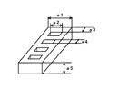
実施例1の発光素子の構造を図6、図7に示す。図6は、第2の電極6および有機層12を一部斜め方向に切欠した斜視図である。図7は、図6に示す発光素子を縦方向に垂直に切断した縦断面図である。マグネシウム−銀合金からなるくし型金属部(反射手段)7を基板形成用枠の中に200μm周期に互いに接触しないよう同一方向へ並べて配置した。くし型金属部7の各部分のサイズは、a1=190μm、a2=90μm、a3=a4=100μm、a5=480μmである。
【0095】
ここに、PES系樹脂のテトラヒドロフラン溶液を静かにキャストした後、溶媒を蒸発させ厚さ500μmの光透過性基板1を得た。得られた光透過性基板1の上面に粗面化処理を行い光拡散部11を形成した後、枠から取り外し、基板形成用枠の底面に接していた面上に、ITOをくし型金属部7のくしの歯に当たる部分の上をわたる80μm幅、120μ間隔のストライプ状でシート抵抗が20Ω/□になるようにスパッタリング法により製膜し、第1の電極2とした。
【0096】
その上に正孔輸送層3として、化合物[化14]を真空蒸着法にて20nm形成した。その上に発光層4として[化1]を真空蒸着法により50nm形成した。
【0097】
次に、電子輸送層5として[化18]を真空蒸着法にて20nm形成した。図では、これら正孔輸送層3、発光層4、および電子輸送層5を一体として有機層12と表現した。
【0098】
次に、第2の電極6としてマグネシウム−銀合金をマスクを通した真空蒸着法によって、くし型金属部7のくしの歯の隙間部の上を通り、第1の電極2のストライプと直交するストライプとなるよう幅80μm、間隔120μmに200nm形成して発光素子を作製した。この素子の各有機EL素子に直流電圧10Vを順次印加したところ、光もれのない14000cd/ m2 の発光が得られた。
【0099】
(実施例2)
実施例2の発光素子の構造を図8に示す。基板形成用枠内の光透過性基板1の上面に粗面化処理を行う代わりに、膜厚100μmで一方の面にSiO2 をスパッタリングにより200nmの膜厚に形成してガスバリア層9とし、他方の面に粗面化処理を行ったPES系樹脂からなる第2の光透過性基板8を、ガスバリア層9と光透過性基板1の上面とが接するように圧着した。この他は、実施例1と同様の手法により発光素子を作製した。この素子の各有機EL素子に直流電圧10Vを順次印加したところ、光もれのない13000cd/ m2 の発光が得られた。
【0100】
(実施例3)
実施例3の発光素子の構造を図9に示す。第2の光透過性基板8の膜厚を80μmとしガスバリア層9の上にPES系樹脂からなる膜厚18μmの第3の光透過性基板10を圧着した後、この第3の光透過性基板10を基板形成用枠内の光透過性基板1の上面に圧着した。これ以外は、実施例2と同様の手法により発光素子を作製した。この素子の各有機EL素子に直流電圧10Vを順次印加したところ、光もれのない13700cd/ m2 の発光が得られた。
【0101】
(実施例4)
実施例4の発光素子の構造を図10に示す。図10は、第2の電極6および有機層12を一部斜め方向に切欠した斜視図である。マグネシウム−銀合金からなる貫通した穴を有する金属部(反射手段)7´を基板形成用枠の中に200μm周期に互いに接触しないよう同一方向へ並べて配置した。貫通した穴を有する金属部7´の構造を図11に示す。各部分のサイズは、a1=190μm、a2=90μm、a3=a4=100μm、a5=480μmである。
【0102】
ここに、PES系樹脂のテトラヒドロフラン溶液を静かにキャストした後、溶媒を蒸発させ厚さ500μmの光透過性基板1を得た。得られた光透過性基板1の上面に粗面化処理を行い光拡散部11を形成した後、枠から取り外し、基板形成用枠の底面に接していた面上に、ITOを貫通した穴を有する金属部7´の穴の部分の上をわたる80μm幅、120μ間隔のストライプ状でシート抵抗が20Ω/□になるようにスパッタリング法により製膜し、第1の電極2とした。
【0103】
その上に正孔輸送層3として、化合物[化14]を真空蒸着法にて20nm形成した。その上に発光層4として[化1]を真空蒸着法により50nm形成した。
【0104】
次に、電子輸送層5として[化18]を真空蒸着法にて20nm形成した。図では、これら正孔輸送層3、発光層4、および電子輸送層5を一体として有機層12と表現した。
【0105】
次に、第2の電極6としてマグネシウム−銀合金をマスクを通した真空蒸着法によって、貫通した穴を有する金属部7´の穴の上を通り、第1の電極2のストライプと直交するストライプとなるよう幅80μm、間隔120μmに200nm形成して発光素子を作製した。この素子の各有機EL素子に直流電圧10Vを順次印加したところ、光もれのない14500cd/ m2 の発光が得られた。
【0106】
(実施例5)
実施例5の発光素子の構造を図12に示す。基板形成用枠内の光透過性基板1の上面に粗面化処理を行う代わりに、膜厚100μmで一方の面にSiO2 をスパッタリングにより200nmの膜厚に形成してガスバリア層9とし、他方の面に粗面化処理を行ったPES系樹脂からなる第2の光透過性基板8を、ガスバリア層9と光透過性基板1の上面とが接するように圧着した。この他は、実施例4と同様の手法により発光素子を作製した。この素子の各有機EL素子に直流電圧10Vを順次印加したところ、光もれのない12900cd/ m2 の発光が得られた。
【0107】
(実施例6)
実施例6の発光素子の構造を図13に示す。第2の光透過性基板8の膜厚を80μmとしガスバリア層9の上にPES系樹脂からなる膜厚18μmの第3の光透過性基板10を圧着した後、この第3の光透過性基板10を基板形成用枠内の光透過性基板1の上面に圧着した。これ以外は、実施例5と同様の手法により発光素子を作製した。この素子の各有機EL素子に直流電圧10Vを順次印加したところ、光もれのない13500cd/ m2 の発光が得られた。
【0108】
次に、以上に説明した発光素子を適用した表示装置について説明する。図14に示すように、本発明の発光素子の駆動回路を各画素(単位発光素子)ごとに、発光部に電流を供給するためのTFT(薄膜トランジスタ)13、画像信号を蓄えるコンデンサ14、コンデンサ14への電荷の蓄積を制御するスイッチングトランジスタ15を設ける。
【0109】
横配線に電圧を印加すると、スイッチングトランジスタ15のゲートに電圧が印加され、ソース−ドレイン間が導通する。この状態で縦配線に電圧を印加すると、コンデンサ14に電荷を蓄えることができる。このコンデンサ14の電荷により、TFT13のゲートに電圧を印加することで、ソース−ドレイン間が導通し、電源が発光部に供給される。
【0110】
上述した単位発光素子をマトリクス状に規則的に配置することにより、アクティブマトリクス型表示装置を得ることができる。横配線、縦配線が接続された図示しない電圧制御回路は、画像信号に基づいて、各画素の発光時間を算出し、横配線、縦配線に印加する電圧、時間、タイミングを決定して、各発光素子を駆動する。
【0111】
なお、上述した実施の形態は、本発明の好適な実施の形態の一例を示すものであり、本発明はそれに限定されることなく、その要旨を逸脱しない範囲内において、種々変形実施が可能である。
【0112】
【発明の効果】
以上の説明から明らかなように、本発明によれば、有機EL素子を用いた発光素子において、光もれがなく、光の取り出し効率の優れた発光素子を実現することが可能となる。したがって、高輝度、低電圧駆動の表示装置を実現することができる。
【図面の簡単な説明】
【図1】本発明の発光素子の断面図である。
【図2】本発明に用いられる有機EL素子の断面図である。
【図3】本発明に用いられる有機EL素子の断面図である。
【図4】本発明に用いられる有機EL素子の断面図である。
【図5】本発明に用いられる有機EL素子の断面図である。
【図6】本発明の実施例1における発光素子の斜視図である。
【図7】本発明の実施例1における発光素子の断面図である。
【図8】本発明の実施例2における発光素子の斜視図である。
【図9】本発明の実施例3における発光素子の斜視図である。
【図10】本発明の実施例4における発光素子の斜視図である。
【図11】本発明の実施例4における金属部の斜視図である。
【図12】本発明の実施例5における発光素子の斜視図である。
【図13】本発明の実施例6における発光素子の斜視図である。
【図14】本発明の発光素子の駆動回路図である。
【符号の説明】
1 光透過性基板
2 第1の電極
3 正孔輸送層
4 発光層
5 電子輸送層
6 第2の電極
7 反射手段(くし型金属部)
7´ 貫通した穴を有する金属部
8 第2の光透過性基板
9 ガスバリア層
10 第3の光透過性基板
11 光拡散部
12 有機層(3、4、5)
13 TFT(薄膜トランジスタ)
14 コンデンサ
15 スイッチングトランジスタ[0001]
BACKGROUND OF THE INVENTION
The present invention relates to a light-emitting element and a display device that use light emitted from an organic electroluminescence element and do not mix light emission from adjacent organic electroluminescence elements and have excellent light extraction efficiency.
[0002]
[Prior art]
An organic electroluminescence (EL) element is a self-luminous element that utilizes the principle that a fluorescent substance emits light by recombination energy between holes injected from an anode and electrons injected from a cathode by applying an electric field. It is. Eastman Kodak's C.I. W. Since Tang et al. Reported a low-voltage driven organic EL element using a stacked element (CWTang, SAVanSlyke, Applied Physics Letters, 51, 913, 1987, etc.) There is a lot of research.
[0003]
In the above report, an organic EL device using tris (8-hydroxyquinolinol aluminum) as a light emitting layer and a triphenyldiamine derivative as a hole transport layer is formed on a glass substrate. The advantages of the stacked structure are that it increases the efficiency of hole injection into the light-emitting layer, blocks the electrons injected from the cathode, increases the generation efficiency of excitons generated by recombination, and generates in the light-emitting layer For example, confining excitons.
[0004]
As in this example, the element structure of the organic EL element includes a hole transport (injection) layer, a two-layer type of an electron transporting light emitting layer, or a hole transport (injection) layer, a light emitting layer, an electron transport (injection) layer. The three-layer type is well known. In such a laminated structure element, the element structure and the formation method are devised in order to increase the recombination efficiency between injected holes and electrons.
[0005]
In an organic EL element, the probability of singlet generation is limited due to the dependence of spin statistics upon carrier recombination, and thus the upper limit of the light emission probability occurs. This upper limit value is known to be approximately 25%.
[0006]
Furthermore, in an organic EL element, light having an emission angle greater than a critical angle cannot be extracted outside due to the influence of the refractive index of the light emitter. For this reason, if the refractive index of the illuminant is 1.6, only about 20% of the total amount of light emission can be effectively used, and the singlet generation probability is about 5% in total as a limit of the energy conversion efficiency. It must be low efficiency (Tetsuo Tsutsui “Current Status and Trends of Organic Electroluminescence”, Monthly Display, vol. 1, No. 3, p11, September 1995). In an organic EL element in which the light emission probability is strongly limited, the light extraction efficiency causes a decrease in efficiency which can be regarded as fatal.
[0007]
As a technique for improving the light extraction efficiency, a light emitting element having an equivalent structure such as an inorganic EL element has been conventionally studied. For example, the method disclosed in JP-A-63-314795 for improving efficiency by providing a substrate with light condensing is effective for an element having a large light emitting area. However, it is difficult to form a lens for providing light condensing in an element with a small pixel area such as a dot matrix display.
[0008]
In addition, a method of introducing a flat layer having an intermediate refractive index between a substrate glass and a light emitter disclosed in Japanese Patent Application Laid-Open No. 62-172691 and forming an antireflection film is a method of extracting light forward. It has the effect of improving efficiency. However, total reflection cannot be prevented. Therefore, even if it is effective for an inorganic EL having a large refractive index, it does not produce a significant improvement effect for an organic EL element that is a light emitter having a relatively low refractive index.
[0009]
Japanese Laid-Open Patent Publication No. 2000-323272 discloses a technique for imparting a function of diffusing light to the surface of the substrate in order to reduce total reflection on the surface that does not contact the organic EL element. However, this technique also has a small effect because the ratio of light totally reflected at the interface between the organic EL element and the glass substrate is large in a conventionally used glass substrate. In addition, when a light-emitting element in which a plurality of organic EL elements are arranged using a substrate having such a light diffusing function, light emitted from the organic EL element reaches an adjacent pixel region. The problem of light leakage occurs when light is observed from a pixel that should be.
[0010]
In order to solve this light leak, Japanese Patent Application Laid-Open No. 11-8070 discloses a method of providing a black mask and a light diffusion layer between a substrate and an organic EL element. However, in this case, a part of the light is absorbed by the black mask, so that the light extraction efficiency is further reduced.
[0011]
[Problems to be solved by the invention]
As described above, methods for preventing light leakage and improving light extraction efficiency of light-emitting elements using organic EL elements are still insufficient. In particular, Japanese Patent Application Laid-Open No. 11-8070 results in sacrificing light extraction efficiency, which has been a concern, in order to prevent light leakage. Therefore, a technology that satisfies both of these requirements is desired. And development of this technology is indispensable for practical use of organic EL elements.
[0012]
The present invention has been made in view of the above circumstances, and provides a high-performance light-emitting element and display device by improving light leakage prevention and light extraction efficiency of a light-emitting element using an organic EL element. With the goal.
[0013]
[Means for Solving the Problems]
In order to achieve this object, the invention described in
[0014]
According to a second aspect of the present invention, there is provided an organic electroluminescence device comprising a transparent first electrode provided on a first light-transmitting substrate and one or more organic thin film layers sandwiched between the second electrodes. And a reflection means for reflecting the light emitted from the organic electroluminescence element, the reflection means is adjacent to the organic electroluminescence element when the plurality of pixels are provided as one pixel. The first light-transmitting substrate has a refractive index larger than the refractive index of the light emitting layer, and prevents light emitted from each pixel from entering the pixel region.
[0015]
According to a third aspect of the present invention, in the first or second aspect of the present invention, the light emitted from the organic electroluminescence element on the surface opposite to the surface in contact with the first electrode of the first light-transmitting substrate. It is characterized by having means for diffusing.
[0016]
According to a fourth aspect of the present invention, in the first aspect of the present invention, the first light transmitting substrate has a refractive index of 1.65 or more and a surface opposite to the surface in contact with the first electrode. And a second light-transmitting substrate having means for diffusing light emitted from the organic electroluminescence element.
[0017]
The invention according to
[0018]
The invention described in
[0019]
The invention according to
[0020]
The invention described in
[0021]
The invention according to
[0022]
The invention according to
[0023]
The invention according to claim 11 is the invention according to any one of
[0024]
A twelfth aspect of the invention is characterized in that, in the invention of any one of the first to eleventh aspects, the reflecting means is made of a metal embedded in the first light transmitting substrate.
[0025]
The invention described in claim 13 is characterized in that, in the invention described in
[0026]
The invention described in
[0027]
The invention according to claim 15 comprises an organic electroluminescence element comprising one or more organic thin film layers sandwiched between a transparent first electrode and a second electrode provided on a light-transmitting substrate, The light transmissive substrate has a refractive index of 1.65 or more, and means for diffusing light emitted from the organic electroluminescence element on a surface opposite to the surface in contact with the first electrode of the light transmissive substrate. It is characterized by having.
[0028]
The invention according to claim 16 comprises an organic electroluminescence device comprising one or more organic thin film layers sandwiched between a transparent first electrode and a second electrode provided on a light-transmitting substrate, The light-transmitting substrate has a refractive index larger than that of the light-emitting layer, and light emitted from the organic electroluminescence element is applied to the surface opposite to the surface in contact with the first electrode of the light-transmitting substrate. It is characterized by having means for diffusing.
[0029]
According to a seventeenth aspect of the present invention, a plurality of first wirings arranged in the same direction, a plurality of second wirings orthogonal to the first wirings, and a first wiring and a second wiring form a matrix. 17. The light-emitting element according to
[0030]
The invention according to claim 18 is the invention according to claim 17, wherein the reflecting means of the light emitting element is formed by arranging a plurality of comb-shaped metal plates, and each of the comb-shaped metal plates functions as an auxiliary electrode. It is characterized by that.
[0031]
The invention according to claim 19 is the invention according to claim 17, wherein the reflecting means of the light emitting element is formed by arranging a plurality of metal plates having through holes, and each of the metal plates having the through holes is auxiliary. It is characterized by functioning as an electrode.
[0032]
DETAILED DESCRIPTION OF THE INVENTION
First, the principle of the present invention will be described. In a light-emitting element using an organic EL element, a substrate having a refractive index larger than the refractive index of the light-emitting layer of the organic EL element or a refractive index larger than 1.65 is used as the light-transmitting substrate. In addition, the light transmissive substrate includes means for reflecting light emitted from the organic EL element so as not to reach an adjacent pixel region. As a result, it has been found that a light emitting element in which light leakage is suppressed can be obtained.
[0033]
In a light-emitting element using an organic EL element, a substrate having a refractive index larger than the refractive index of the light-emitting layer of the organic EL element or a refractive index larger than 1.65 is used as the light-transmitting substrate. At the same time, it has a function of diffusing the light into the surface where the light is emitted into the air. As a result, it has been found that a light emitting element in which light leakage is suppressed and light extraction efficiency is improved can be obtained.
[0034]
In the conventional organic EL device, light emitted from the light emitting layer is only about 20% of the light emitted from the light emitting layer due to loss at the two interfaces of the organic EL device-substrate interface and the substrate-air interface. It cannot be extracted effectively. When a substrate having a refractive index larger than the refractive index of the light emitting layer or a refractive index larger than 1.65 is used as the light transmissive substrate, the proportion of light lost at the organic EL element-substrate interface can be reduced. . However, this alone alone increases the proportion of light lost at the substrate-air interface, and the overall light extraction efficiency does not change.
[0035]
However, by having the function of diffusing light at the substrate-air interface of this substrate, the ratio of the light that is not emitted from the substrate into the air is reduced because light is emitted and reflected in various directions at the interface, and the organic EL Combined with loss reduction at the element-substrate interface, the light extraction efficiency is greatly improved.
[0036]
However, simply adding a function of diffusing light to a substrate having a refractive index smaller than 1.65 or smaller than the refractive index of the light emitting layer causes a very large ratio of light confined in the organic EL element. The light extraction efficiency is not improved, but the extraction efficiency is lowered due to other factors.
[0037]
Furthermore, light leakage is improved by providing means for reflecting the light so as not to reach the adjacent pixel region. The light that is emitted at an angle to reach the adjacent pixel area when there is no reflection means is reflected in the pixel area where the organic EL element that is the emission source is present, so that the light loss is small.
[0038]
As described above, in order to effectively suppress light leakage, it is desirable that the light reflected once by the reflecting means does not reach the adjacent pixel region. In the cross section (FIG. 1) cut along a plane perpendicular to both the reflecting surface of the reflecting means and the light-transmitting substrate surface, the distance D between the centers of the reflecting means surrounding one organic EL element and the same organic EL element side. It is assumed that the distance d between the two reflecting surfaces arranged has a relationship of t = d / D. And the height of the said reflection means measured from the contact surface with the 1st electrode of a light transmissive substrate is h, The surface from which light is radiate | emitted in the air from the contact surface with the 1st electrode of a light transmissive substrate If the distance up to is H, the following
[0039]
[Expression 1]
It can be seen that h is preferably 4t / (1 + 3t) times or more of H.
[0041]
In addition, when the surface where light is emitted from the substrate portion having a high refractive index into the air is a normal flat surface, total reflection occurs due to the difference in refractive index from the air. The extraction efficiency is not improved. On the other hand, by providing the surface with a function of diffusing light, light is repeatedly emitted and reflected at various angles, thereby increasing the proportion of light extracted outside the substrate. As described above, the ratio of light incident from the organic EL element into the substrate having a high refractive index is increased as compared with the case where a conventional substrate having a low refractive index is used. Efficiency is greatly improved.
[0042]
Hereinafter, embodiments of the present invention will be described in detail with reference to the accompanying drawings.
[0043]
The element structure of the light-emitting element in the present invention is only required to be a structure having one or a plurality of organic layers including at least a light-emitting layer between both the first electrode and the second electrode. There are no restrictions. One of the first electrode and the second electrode serves as an anode and the other serves as a cathode. When the first electrode is an anode and the second electrode is a cathode, structural examples of the organic EL element are shown in FIGS.
[0044]
In the light-emitting element shown in FIG. 2, a light-transmitting
[0045]
In addition, for the purpose of improving charge injection characteristics between these organic layers and between organic layer electrodes, suppressing dielectric breakdown, or improving luminous efficiency, inorganic such as lithium fluoride, magnesium fluoride, silicon oxide, silicon dioxide, silicon nitride, etc. Thin film layer made of dielectric material, insulator, mixed layer of organic layer and electrode material or metal, or organic polymer thin film such as polyaniline, polyacetylene derivative, polydiacetylene derivative, polyvinylcarbazole derivative, polyparaphenylene vinylene derivative, etc. You can insert it.
[0046]
The light emitting material used in the present invention is not particularly limited, and any compound that is usually used as a light emitting material may be used.
[0047]
[Chemical 1]
[Chemical formula 2]
[Chemical 3]
[Formula 4]
[Chemical formula 5]
For example, the above-described tris (8-quinolinol) aluminum complex (Alq3) [Chemical Formula 1], bisdiphenylvinylbiphenyl (BDPVBi) [Chemical Formula 2], 1,3-bis (pt-butylphenyl-1,3,4) -Oxadiazolyl) phenyl (OXD-7) [Chemical Formula 3], N, N′-bis (2,5-di-t-butylphenyl) perylenetetracarboxylic acid diimide (BPPC) [Chemical Formula 4], 1, In addition to low-molecular light-emitting materials such as 4-bis (Np-tolyl-N-4- (4-methylstyryl) phenylamino) naphthalene [Chem. 5], high-molecular light-emitting materials such as polyphenylene vinylene polymers can also be used. It is.
[0053]
In addition, a layer in which a charge transport material is doped with a fluorescent material can be used as a light emitting material.
[0054]
[Chemical 6]
[Chemical 7]
[Chemical 8]
[Chemical 9]
[Chemical Formula 10]
Embedded image
Embedded image
For example, a quinolinol metal complex such as the above Alq3 [Chemical Formula 1] is added to 4-dicyanomethylene-2-methyl-6- (p-dimethylaminostyryl) -4H-pyran (DCM) [Chemical Formula 6], 2,3- A layer doped with a quinacridone derivative such as quinacridone [Chemical Formula 7], a coumarin derivative such as 3- (2′-benzothiazole) -7-diethylaminocoumarin [Chemical Formula 8], or an electron transport material bis (2-methyl-8-hydroxy) Quinoline) -4-phenylphenol-aluminum complex [Chemical 9] doped with condensed polycyclic aromatics such as perylene [Chemical 10], or
[0062]
The hole transport material used in the present invention is not particularly limited, and any compound that is usually used as a hole transport material may be used.
[0063]
Embedded image
Embedded image
Embedded image
Embedded image
Embedded image
For example, bis (di (p-tolyl) aminophenyl) -1,1-cyclohexane [Chemical Formula 13], TPD [Chemical Formula 11], N, N′-diphenyl-NN—bis (1-naphthyl) -1, And triphenyldiamines such as 1′-biphenyl) -4,4′-diamine (NPB) [Chemical Formula 14], starburst type molecules (Chemical Formula 15 to Chemical Formula 17) and the like.
[0069]
The electron transport material used in the present invention is not particularly limited, and any compound that is usually used as an electron transport material may be used.
[0070]
Embedded image
Embedded image
Embedded image
Embedded image
Embedded image
Embedded image
Embedded image
For example, 2- (4-biphenylyl) -5- (4-t-butylphenyl) -1,3,4-oxadiazole (Bu-PBD) [Chem. 18], OXD-7 [Chem. Examples thereof include diazole derivatives, triazole derivatives ([Chemical Formula 19], [Chemical Formula 20] and the like) and quinolinol-based metal complexes ([Chemical Formula 1], [Chemical Formula 9], [Chemical Formula 21] to [Chemical Formula 24] and the like).
[0078]
The anode of the organic thin film EL element plays a role of injecting holes into the hole transport layer, and it is effective to have a work function of 4.5 eV or more. Specific examples of the anode material used in the present invention include indium tin oxide alloy (ITO), tin oxide (NESA), gold, silver, platinum, copper, and the like.
[0079]
The cathode is preferably made of a material having a small work function for the purpose of injecting electrons into the electron transport zone or the light emitting layer. The cathode material is not particularly limited, and specifically, indium, aluminum, magnesium, magnesium-indium alloy, magnesium-aluminum alloy, aluminum-lithium alloy, aluminum-scandium-lithium alloy, magnesium-silver alloy and the like can be used.
[0080]
The method for forming each layer in the light emitting device of the present invention is not particularly limited. Conventionally known methods such as vacuum deposition and spin coating can be used. The organic thin film layer containing the above-mentioned compound used in the organic EL device of the present invention is prepared by vacuum deposition, molecular beam deposition (MBE), dipping of a solution dissolved in a solvent, spin coating, casting, bar It can be formed by a known method such as a coating method or a roll coating method.
[0081]
The thickness of the light emitting layer, the hole transport layer, and the electron transport layer of the light emitting device in the present invention is not particularly limited. However, if the film thickness is too thin, defects such as pinholes are likely to occur. On the other hand, if the thickness is too large, a high applied voltage is required and the efficiency is deteriorated.
[0082]
The light-transmitting substrate in the present invention has a refractive index larger than the refractive index of the light emitting layer or a refractive index larger than 1.65. Examples of materials that can be used for such a substrate include high refractive index optical glass such as FD-11, LaK3, BaF10, LaF2, SF13, and SFS1, and inorganic materials such as sapphire glass, titania glass, and ZnSe. Examples thereof include sulfur-containing resins represented by polyethersulfone (PES) resins.
[0083]
Further, the light-transmitting substrate in the present invention imparts a function of diffusing light to a surface not in contact with the first electrode, or diffuses light made of the above substrate material to a surface not in contact with the first electrode. By providing the second light-transmitting substrate having a function, light extraction efficiency can be improved.
[0084]
The function of diffusing light is not only a method of providing an uneven shape on the surface from which light is emitted, but also a light-transmitting microscopic material made of a material having a refractive index different from that of the substrate material, such as a light-transmitting resin or glass having a low refractive index. It can be realized by a technique of arranging a sphere, a light-transmitting fiber, a cylindrical lens, or the like on a surface from which light is emitted.
[0085]
The second light-transmitting substrate can be formed using any material that can be used for the light-transmitting substrate. In particular, a combination in which the refractive index of the second light-transmitting substrate is equal to or higher than the refractive index of the light-transmitting substrate is more preferable.
[0086]
Further, when a substrate made of a resin is used as the second light transmissive substrate, the light transmissive substrate is used to prevent a gas that adversely affects the characteristics of the organic EL element from entering the light transmissive substrate. Deterioration of the organic EL element can be suppressed by providing a gas barrier layer between the first light transmissive substrate and the second light transmissive substrate. As this gas barrier layer, it is effective to use a material having a gas barrier property against water and oxygen. 2 , SiNx, SiOxNy, and the like formed by a conventionally known film formation method such as sputtering can be used.
[0087]
In order to improve the adhesion between the gas barrier layer and the light transmissive substrate, it is also effective to provide a third light transmissive substrate between the gas barrier layer and the light transmissive substrate. Examples of the material that can be used for the third light transmissive substrate include materials that can be used to form the light transmissive substrate.
[0088]
As the reflection means in the present invention, any reflection means can be used as long as it has a function of reflecting light introduced from the organic EL element to the light-transmitting substrate and preventing it from reaching the adjacent pixel region. For example, a wall-like protrusion in which a material having a lower refractive index than the substrate material of the light-transmitting substrate is embedded in the light-transmitting substrate, or a metal that can reflect light obtained from the organic EL element is embedded in the light-transmitting substrate. And a mirror formed in this manner.
[0089]
Further, in order to suppress light leakage more efficiently, the centers of the reflecting means surrounding one organic EL element are cut in a cross section cut by a plane perpendicular to both the reflecting surface of the reflecting means and the light transmitting substrate surface. When the distance D and the distance d between the two reflecting surfaces arranged on the same organic EL element side are in the relationship of t = d / D, the above-mentioned as viewed from the contact surface with the first electrode of the light-transmitting substrate As described above, the height of the reflecting means is desirably 4t / (1 + 3t) times or more of the distance from the contact surface with the first electrode of the light-transmitting substrate to the surface where the light is radiated into the air. Street.
[0090]
When the reflecting means of the present invention is formed of a metal embedded in a substrate, the reflecting means is formed so as to conduct in an appropriate direction, and the first electrode is electrically connected to the reflecting means. The function as an auxiliary electrode of the first electrode can be imparted to the reflecting means. Thereby, the wiring resistance of the first electrode can be reduced, and the power consumption of the entire light emitting element can be reduced.
[0091]
As the metal forming the reflecting means of the present invention, any metal having properties of reflecting light obtained from an organic EL element, or an alloy thereof can be used. However, when the first electrode and the metal portion are electrically connected and the organic EL element is driven using the light-transmitting first electrode as an anode, an organic thin film of an organic EL element such as gold or silver is used. When a metal capable of hole injection is used for the layer, it is necessary to provide an insulator between the metal portion and the organic thin film layer.
[0092]
This requires an extra process and increases costs. From this, it is desirable that the metal used for the reflecting means is a metal having a work function of 4.3 eV or less that cannot inject holes into the organic thin film layer. Examples of such metals include indium, aluminum, magnesium, magnesium-indium alloy, magnesium-aluminum alloy, aluminum-lithium alloy, aluminum-scandium-lithium alloy, and magnesium-silver alloy.
[0093]
EXAMPLES Hereinafter, although this invention is demonstrated in detail based on an Example, this invention is not limited to a following example, unless the summary is exceeded.
[0094]
Example 1
The structure of the light-emitting element of Example 1 is shown in FIGS. FIG. 6 is a perspective view in which the
[0095]
Here, a tetrahydrofuran solution of the PES resin was gently cast, and then the solvent was evaporated to obtain a
[0096]
A 20 [nm] thick compound [Chemical Formula 14] was formed thereon as a
[0097]
Next, as the
[0098]
Next, as a
[0099]
(Example 2)
The structure of the light-emitting element of Example 2 is shown in FIG. Instead of roughening the upper surface of the light-transmitting
[0100]
(Example 3)
The structure of the light-emitting element of Example 3 is shown in FIG. After the second light-transmitting
[0101]
(Example 4)
The structure of the light-emitting element of Example 4 is shown in FIG. FIG. 10 is a perspective view in which the
[0102]
Here, a tetrahydrofuran solution of the PES resin was gently cast, and then the solvent was evaporated to obtain a
[0103]
A 20 [nm] thick compound [Chemical Formula 14] was formed thereon as a
[0104]
Next, as the
[0105]
Next, a stripe perpendicular to the stripe of the
[0106]
(Example 5)
The structure of the light-emitting element of Example 5 is shown in FIG. Instead of roughening the upper surface of the light-transmitting
[0107]
(Example 6)
The structure of the light-emitting element of Example 6 is shown in FIG. After the second light-transmitting
[0108]
Next, a display device using the light-emitting element described above will be described. As shown in FIG. 14, the driving circuit of the light emitting device of the present invention is provided with a TFT (thin film transistor) 13 for supplying current to the light emitting portion for each pixel (unit light emitting device), a
[0109]
When a voltage is applied to the horizontal wiring, a voltage is applied to the gate of the switching transistor 15 and the source-drain is made conductive. When a voltage is applied to the vertical wiring in this state, charges can be stored in the
[0110]
An active matrix display device can be obtained by regularly arranging the above-described unit light emitting elements in a matrix. A voltage control circuit (not shown) to which the horizontal wiring and the vertical wiring are connected calculates the light emission time of each pixel based on the image signal, determines the voltage, time, and timing applied to the horizontal wiring and the vertical wiring. The light emitting element is driven.
[0111]
The above-described embodiment shows an example of a preferred embodiment of the present invention, and the present invention is not limited thereto, and various modifications can be made without departing from the scope of the invention. is there.
[0112]
【The invention's effect】
As is apparent from the above description, according to the present invention, in a light emitting element using an organic EL element, it is possible to realize a light emitting element having no light leakage and excellent light extraction efficiency. Therefore, a display device with high brightness and low voltage can be realized.
[Brief description of the drawings]
FIG. 1 is a cross-sectional view of a light emitting device of the present invention.
FIG. 2 is a cross-sectional view of an organic EL element used in the present invention.
FIG. 3 is a cross-sectional view of an organic EL element used in the present invention.
FIG. 4 is a cross-sectional view of an organic EL element used in the present invention.
FIG. 5 is a cross-sectional view of an organic EL element used in the present invention.
FIG. 6 is a perspective view of a light emitting element in Example 1 of the present invention.
7 is a cross-sectional view of a light-emitting element in Example 1 of the present invention. FIG.
FIG. 8 is a perspective view of a light emitting device in Example 2 of the present invention.
FIG. 9 is a perspective view of a light emitting device in Example 3 of the present invention.
FIG. 10 is a perspective view of a light emitting device in Example 4 of the present invention.
FIG. 11 is a perspective view of a metal part in
12 is a perspective view of a light emitting device in Example 5 of the present invention. FIG.
FIG. 13 is a perspective view of a light emitting device in Example 6 of the present invention.
FIG. 14 is a drive circuit diagram of a light emitting device of the present invention.
[Explanation of symbols]
1 Light transmissive substrate
2 First electrode
3 Hole transport layer
4 Light emitting layer
5 Electron transport layer
6 Second electrode
7 Reflection means (comb-shaped metal part)
7 'Metal part with a through hole
8 Second light-transmitting substrate
9 Gas barrier layer
10 Third light transmitting substrate
11 Light diffusion part
12 Organic layers (3, 4, 5)
13 TFT (Thin Film Transistor)
14 capacitors
15 Switching transistor
Claims (16)
前記第1の光透過性基板が前記有機エレクトロルミネッセンス素子から放射される光を反射する反射手段と、を少なくとも備え、
前記反射手段は、前記有機エレクトロルミネッセンス素子を1画素として複数画素を備えたとき、隣接する画素領域への各画素から放射される光の進入を阻止し、
前記第1の光透過性基板は、1.65以上の屈折率を有し、
前記反射手段の反射面と、前記第1の光透過性基板面とに共に垂直な面で切断した断面において、1つの前記有機エレクトロルミネッセンス素子を囲む反射手段の内、対向している反射手段の中心どうしの距離Dと、該対向している反射手段の該有機エレクトロルミネッセンス素子側の反射面の間隔dとをt=d/Dとして、
前記第1の光透過性基板の前記第1の電極との接触面からみた前記反射手段の高さが、前記第1の光透過性基板の前記第1の電極との接触面から前記光が空気中へ輻射される面までの距離の4t/(1+3t)倍以上であることを特徴とする発光素子。An organic electroluminescent element comprising one or more organic thin film layers sandwiched between a transparent first electrode and a second electrode provided on a first light-transmitting substrate;
The first light-transmitting substrate includes at least reflecting means for reflecting light emitted from the organic electroluminescence element;
When the reflection means includes a plurality of pixels with the organic electroluminescence element as one pixel, it prevents light emitted from each pixel from entering an adjacent pixel region,
The first light transmitting substrate, have a 1.65 or more refractive index,
Of the reflecting means surrounding one organic electroluminescence element, the reflecting means facing each other in a cross section cut by a plane perpendicular to both the reflecting surface of the reflecting means and the first light transmitting substrate surface. The distance D between the centers and the distance d between the reflecting surfaces on the organic electroluminescence element side of the opposing reflecting means are t = d / D,
The height of the reflecting means as viewed from the contact surface of the first light transmissive substrate with the first electrode is such that the light is transmitted from the contact surface of the first light transmissive substrate with the first electrode. A light emitting element characterized by being at least 4t / (1 + 3t) times the distance to the surface radiated into the air .
前記第1の光透過性基板が前記有機エレクトロルミネッセンス素子から放射される光を反射する反射手段と、を少なくとも備え、
前記反射手段は、前記有機エレクトロルミネッセンス素子を1画素として複数画素を備えたとき、隣接する画素領域への各画素から放射される光の進入を阻止し、
前記第1の光透過性基板は、発光層の屈折率よりも大きな屈折率を有し、
前記反射手段の反射面と、前記第1の光透過性基板面とに共に垂直な面で切断した断面において、1つの前記有機エレクトロルミネッセンス素子を囲む反射手段の内、対向している反射手段の中心どうしの距離Dと、該対向している反射手段の該有機エレクトロルミネッセンス素子側の反射面の間隔dとをt=d/Dとして、
前記第1の光透過性基板の前記第1の電極との接触面からみた前記反射手段の高さが、前記第1の光透過性基板の前記第1の電極との接触面から前記光が空気中へ輻射される面までの距離の4t/(1+3t)倍以上であることを特徴とする発光素子。An organic electroluminescent element comprising one or more organic thin film layers sandwiched between a transparent first electrode and a second electrode provided on a first light-transmitting substrate;
The first light-transmitting substrate includes at least reflecting means for reflecting light emitted from the organic electroluminescence element;
When the reflection means includes a plurality of pixels with the organic electroluminescence element as one pixel, it prevents light emitted from each pixel from entering an adjacent pixel region,
The first light transmitting substrate, have a refractive index greater than the refractive index of the light-emitting layer,
Of the reflecting means surrounding one organic electroluminescence element, the reflecting means facing each other in a cross section cut by a plane perpendicular to both the reflecting surface of the reflecting means and the first light transmitting substrate surface. The distance D between the centers and the distance d between the reflecting surfaces on the organic electroluminescence element side of the opposing reflecting means are t = d / D,
The height of the reflecting means as viewed from the contact surface of the first light transmissive substrate with the first electrode is such that the light is transmitted from the contact surface of the first light transmissive substrate with the first electrode. A light emitting element characterized by being at least 4t / (1 + 3t) times the distance to the surface radiated into the air .
前記第1の配線と直交する複数の第2の配線と、
前記第1の配線と前記第2の配線とによりマトリクス状に形成された画素領域に対応して配置された請求項1〜13のいずれか1項に記載の発光素子と、
前記第1の配線と前記第2の配線とを制御する電圧制御回路と、
前記発光素子に駆動電流を供給する共通給電線と、を備え、
前記各画素は、画像信号がゲート電極に印加され、前記共通給電線と前記有機エレクトルミネッセンスとの導通を制御する薄膜トランジスタを有することを特徴とする表示装置。A plurality of first wires arranged in the same direction;
A plurality of second wires orthogonal to the first wires;
The light emitting device according to any one of claims 1 to 13 , wherein the light emitting device is disposed corresponding to a pixel region formed in a matrix by the first wiring and the second wiring,
A voltage control circuit for controlling the first wiring and the second wiring;
A common power supply line for supplying a driving current to the light emitting element,
Each of the pixels includes a thin film transistor that is applied with an image signal to a gate electrode and controls conduction between the common power supply line and the organic electroluminescence.
Priority Applications (4)
| Application Number | Priority Date | Filing Date | Title |
|---|---|---|---|
| JP2001230414A JP4302914B2 (en) | 2001-07-30 | 2001-07-30 | LIGHT EMITTING ELEMENT AND DISPLAY DEVICE |
| US10/202,214 US6771018B2 (en) | 2001-07-30 | 2002-07-24 | Light-emitting device and display device employing electroluminescence with no light leakage and improved light extraction efficiency |
| KR10-2002-0044612A KR100478525B1 (en) | 2001-07-30 | 2002-07-29 | Light-Emitting Device and Display Device Employing Electroluminescence with no Light Leakage and Improved Light Extraction Efficiency |
| CNB021271844A CN1181708C (en) | 2001-07-30 | 2002-07-30 | Light emitting device and display device using electroluminescence |
Applications Claiming Priority (1)
| Application Number | Priority Date | Filing Date | Title |
|---|---|---|---|
| JP2001230414A JP4302914B2 (en) | 2001-07-30 | 2001-07-30 | LIGHT EMITTING ELEMENT AND DISPLAY DEVICE |
Publications (2)
| Publication Number | Publication Date |
|---|---|
| JP2003045643A JP2003045643A (en) | 2003-02-14 |
| JP4302914B2 true JP4302914B2 (en) | 2009-07-29 |
Family
ID=19062631
Family Applications (1)
| Application Number | Title | Priority Date | Filing Date |
|---|---|---|---|
| JP2001230414A Expired - Lifetime JP4302914B2 (en) | 2001-07-30 | 2001-07-30 | LIGHT EMITTING ELEMENT AND DISPLAY DEVICE |
Country Status (4)
| Country | Link |
|---|---|
| US (1) | US6771018B2 (en) |
| JP (1) | JP4302914B2 (en) |
| KR (1) | KR100478525B1 (en) |
| CN (1) | CN1181708C (en) |
Cited By (1)
| Publication number | Priority date | Publication date | Assignee | Title |
|---|---|---|---|---|
| US10615240B2 (en) | 2015-04-28 | 2020-04-07 | Samsung Display Co., Ltd. | Organic light-emitting diode display |
Families Citing this family (29)
| Publication number | Priority date | Publication date | Assignee | Title |
|---|---|---|---|---|
| JP2004020746A (en) * | 2002-06-13 | 2004-01-22 | Sumitomo Bakelite Co Ltd | Light emitting device substrate and light emitting device using the same |
| US7850339B2 (en) | 2003-01-30 | 2010-12-14 | Touchsensor Technologies, Llc | Display having thin cross-section and/or multi-colored output |
| US7175304B2 (en) * | 2003-01-30 | 2007-02-13 | Touchsensor Technologies, Llc | Integrated low profile display |
| JP4703108B2 (en) * | 2003-09-10 | 2011-06-15 | 三星モバイルディスプレイ株式會社 | Light emitting element substrate and light emitting element using the same |
| JP4771040B2 (en) * | 2003-09-17 | 2011-09-14 | スタンレー電気株式会社 | EL lighting device |
| JP2005174701A (en) * | 2003-12-10 | 2005-06-30 | Toyota Industries Corp | Electroluminescent device |
| JP3819927B2 (en) * | 2004-06-03 | 2006-09-13 | 日東電工株式会社 | Transparent conductive film |
| WO2006016153A1 (en) * | 2004-08-10 | 2006-02-16 | Cambridge Display Technology Limited | Light emissive device |
| JP4732084B2 (en) * | 2004-09-21 | 2011-07-27 | 三星モバイルディスプレイ株式會社 | SUBSTRATE FOR LIGHT EMITTING ELEMENT, ITS MANUFACTURING METHOD, ELECTRODE FOR LIGHT EMITTING ELEMENT, AND LIGHT EMITTING ELEMENT HAVING THE SAME |
| KR101197045B1 (en) | 2005-02-07 | 2012-11-06 | 삼성디스플레이 주식회사 | Display device and manufacturing method thereof |
| US9530968B2 (en) * | 2005-02-15 | 2016-12-27 | Semiconductor Energy Laboratory Co., Ltd. | Light emitting element and light emitting device |
| US7535163B2 (en) * | 2006-02-22 | 2009-05-19 | Tpo Displays Corp. | System for displaying images including electroluminescent device and method for fabricating the same |
| US20080117362A1 (en) * | 2006-11-21 | 2008-05-22 | 3M Innovative Properties Company | Organic Light Emitting Diode Devices With Optical Microstructures |
| JP5577012B2 (en) * | 2007-05-03 | 2014-08-20 | 株式会社カネカ | Multilayer substrate and manufacturing method thereof |
| WO2009004560A2 (en) * | 2007-07-04 | 2009-01-08 | Koninklijke Philips Electronics N.V. | A method for forming a patterned layer on a substrate |
| US8179034B2 (en) * | 2007-07-13 | 2012-05-15 | 3M Innovative Properties Company | Light extraction film for organic light emitting diode display and lighting devices |
| US20090015142A1 (en) * | 2007-07-13 | 2009-01-15 | 3M Innovative Properties Company | Light extraction film for organic light emitting diode display devices |
| US20100110551A1 (en) * | 2008-10-31 | 2010-05-06 | 3M Innovative Properties Company | Light extraction film with high index backfill layer and passivation layer |
| US7957621B2 (en) * | 2008-12-17 | 2011-06-07 | 3M Innovative Properties Company | Light extraction film with nanoparticle coatings |
| US8686630B2 (en) | 2009-02-09 | 2014-04-01 | Konica Minolta Holdings, Inc. | Organic electroluminescence element and illumination device using the same |
| JP2010199183A (en) * | 2009-02-24 | 2010-09-09 | Sanyo Electric Co Ltd | Package for light emitting device and method of manufacturing the same |
| TWI527781B (en) * | 2009-07-08 | 2016-04-01 | 日本電氣硝子股份有限公司 | glass plate |
| US8247838B2 (en) * | 2009-12-18 | 2012-08-21 | United Microelectronics Corporation | Light emitting diode with semiconductor layer having different resistance at different regions |
| JP5578987B2 (en) * | 2010-08-23 | 2014-08-27 | ユー・ディー・シー アイルランド リミテッド | Fine particle layer transfer material, organic electroluminescence device and method for producing the same |
| WO2014064833A1 (en) * | 2012-10-26 | 2014-05-01 | パイオニア株式会社 | Light emitting device, and manufacturing method for light emitting device |
| CN103346269B (en) * | 2013-07-15 | 2016-03-09 | 广州新视界光电科技有限公司 | A kind of semitransparent electrode and there is the organic electroluminescence device of this semitransparent electrode |
| KR102295610B1 (en) * | 2013-12-27 | 2021-08-30 | 엘지디스플레이 주식회사 | Organic light emitting diode display device |
| JPWO2015115175A1 (en) * | 2014-01-31 | 2017-03-23 | コニカミノルタ株式会社 | Organic electroluminescence device and method for manufacturing the same |
| JP6049925B2 (en) * | 2016-02-24 | 2016-12-21 | ユー・ディー・シー アイルランド リミテッド | Organic electroluminescence device |
Family Cites Families (7)
| Publication number | Priority date | Publication date | Assignee | Title |
|---|---|---|---|---|
| JPH0766856B2 (en) | 1986-01-24 | 1995-07-19 | 株式会社小松製作所 | Thin film EL device |
| JP2670572B2 (en) | 1987-06-18 | 1997-10-29 | 株式会社小松製作所 | Thin film EL element |
| JP3065458B2 (en) * | 1993-07-20 | 2000-07-17 | シャープ株式会社 | EL element |
| JPH118070A (en) | 1997-06-17 | 1999-01-12 | Casio Comput Co Ltd | Display device |
| JP2000231985A (en) * | 1999-02-12 | 2000-08-22 | Denso Corp | Organic EL device |
| JP2000323272A (en) | 1999-05-14 | 2000-11-24 | Casio Comput Co Ltd | Flat light source |
| JP2001167889A (en) * | 1999-12-08 | 2001-06-22 | Sharp Corp | Display device |
-
2001
- 2001-07-30 JP JP2001230414A patent/JP4302914B2/en not_active Expired - Lifetime
-
2002
- 2002-07-24 US US10/202,214 patent/US6771018B2/en not_active Expired - Lifetime
- 2002-07-29 KR KR10-2002-0044612A patent/KR100478525B1/en not_active Expired - Lifetime
- 2002-07-30 CN CNB021271844A patent/CN1181708C/en not_active Expired - Lifetime
Cited By (3)
| Publication number | Priority date | Publication date | Assignee | Title |
|---|---|---|---|---|
| US10615240B2 (en) | 2015-04-28 | 2020-04-07 | Samsung Display Co., Ltd. | Organic light-emitting diode display |
| US11158698B2 (en) | 2015-04-28 | 2021-10-26 | Samsung Display Co., Ltd. | Organic light-emitting diode display |
| USRE50012E1 (en) | 2015-04-28 | 2024-06-11 | Samsung Display Co., Ltd. | Organic light-emitting diode display |
Also Published As
| Publication number | Publication date |
|---|---|
| US6771018B2 (en) | 2004-08-03 |
| JP2003045643A (en) | 2003-02-14 |
| US20030043571A1 (en) | 2003-03-06 |
| KR100478525B1 (en) | 2005-03-28 |
| CN1400851A (en) | 2003-03-05 |
| CN1181708C (en) | 2004-12-22 |
| KR20030011657A (en) | 2003-02-11 |
Similar Documents
| Publication | Publication Date | Title |
|---|---|---|
| JP4302914B2 (en) | LIGHT EMITTING ELEMENT AND DISPLAY DEVICE | |
| KR100685805B1 (en) | Light emitting device, manufacturing method thereof and display device using same | |
| JP4470627B2 (en) | Optical substrate, light emitting element, and display device | |
| KR101295988B1 (en) | Stacked organic electroluminescent devices | |
| JP6049797B2 (en) | Method for manufacturing light emitting device | |
| KR100472502B1 (en) | Organic electro luminescence display device | |
| JP4263415B2 (en) | ORGANIC LIGHT EMITTING ELEMENT AND DISPLAY DEVICE USING THE ELEMENT | |
| US6524884B1 (en) | Method for fabricating an organic electroluminescene device having organic field effect transistor and organic eloectroluminescence diode | |
| US7928537B2 (en) | Organic electroluminescent device | |
| US6483123B1 (en) | Organic electroluminescent device having organic field effect transistor and organic light-emitting diode and method for fabricating the same | |
| KR102695219B1 (en) | Organic Light Emitting Diode Display Device | |
| JP2004145244A (en) | Display device | |
| CN1604710A (en) | Organic Electroluminescent Devices | |
| WO2007043697A9 (en) | Light emitting device and display device | |
| JPH11214163A (en) | Organic electroluminescence device and method of manufacturing the same | |
| JP2004227944A (en) | Display device manufacturing method | |
| KR100471460B1 (en) | Light-emitting device | |
| WO2013146350A1 (en) | Light emitting apparatus and method for manufacturing light emitting apparatus | |
| JP2007294441A (en) | Functional element | |
| KR101680705B1 (en) | Organic electroluminescent device and method of fabricating the same | |
| KR20170006336A (en) | Organic light emitting diode, manufacturing method for the same, and organic light emitting display device having the organic light emitting diode | |
| JP4893816B2 (en) | OPTICAL SUBSTRATE, LIGHT EMITTING ELEMENT, DISPLAY DEVICE AND METHOD FOR PRODUCING THEM | |
| KR100770577B1 (en) | Organic light emitting device | |
| JP2007317519A (en) | Organic electroluminescence device |
Legal Events
| Date | Code | Title | Description |
|---|---|---|---|
| A521 | Request for written amendment filed |
Free format text: JAPANESE INTERMEDIATE CODE: A821 Effective date: 20040316 |
|
| A711 | Notification of change in applicant |
Free format text: JAPANESE INTERMEDIATE CODE: A711 Effective date: 20040316 |
|
| A521 | Request for written amendment filed |
Free format text: JAPANESE INTERMEDIATE CODE: A821 Effective date: 20040702 |
|
| A621 | Written request for application examination |
Free format text: JAPANESE INTERMEDIATE CODE: A621 Effective date: 20040702 |
|
| A131 | Notification of reasons for refusal |
Free format text: JAPANESE INTERMEDIATE CODE: A131 Effective date: 20080415 |
|
| A521 | Request for written amendment filed |
Free format text: JAPANESE INTERMEDIATE CODE: A523 Effective date: 20080714 |
|
| A02 | Decision of refusal |
Free format text: JAPANESE INTERMEDIATE CODE: A02 Effective date: 20080812 |
|
| A521 | Request for written amendment filed |
Free format text: JAPANESE INTERMEDIATE CODE: A523 Effective date: 20081110 Free format text: JAPANESE INTERMEDIATE CODE: A821 Effective date: 20081110 |
|
| A711 | Notification of change in applicant |
Free format text: JAPANESE INTERMEDIATE CODE: A712 Effective date: 20081208 |
|
| A911 | Transfer to examiner for re-examination before appeal (zenchi) |
Free format text: JAPANESE INTERMEDIATE CODE: A911 Effective date: 20090223 |
|
| A711 | Notification of change in applicant |
Free format text: JAPANESE INTERMEDIATE CODE: A712 Effective date: 20090225 |
|
| TRDD | Decision of grant or rejection written | ||
| A01 | Written decision to grant a patent or to grant a registration (utility model) |
Free format text: JAPANESE INTERMEDIATE CODE: A01 Effective date: 20090324 |
|
| A01 | Written decision to grant a patent or to grant a registration (utility model) |
Free format text: JAPANESE INTERMEDIATE CODE: A01 |
|
| A61 | First payment of annual fees (during grant procedure) |
Free format text: JAPANESE INTERMEDIATE CODE: A61 Effective date: 20090423 |
|
| FPAY | Renewal fee payment (event date is renewal date of database) |
Free format text: PAYMENT UNTIL: 20120501 Year of fee payment: 3 |
|
| R150 | Certificate of patent or registration of utility model |
Free format text: JAPANESE INTERMEDIATE CODE: R150 Ref document number: 4302914 Country of ref document: JP Free format text: JAPANESE INTERMEDIATE CODE: R150 |
|
| FPAY | Renewal fee payment (event date is renewal date of database) |
Free format text: PAYMENT UNTIL: 20130501 Year of fee payment: 4 |
|
| R250 | Receipt of annual fees |
Free format text: JAPANESE INTERMEDIATE CODE: R250 |
|
| FPAY | Renewal fee payment (event date is renewal date of database) |
Free format text: PAYMENT UNTIL: 20130501 Year of fee payment: 4 |
|
| S111 | Request for change of ownership or part of ownership |
Free format text: JAPANESE INTERMEDIATE CODE: R313111 |
|
| S531 | Written request for registration of change of domicile |
Free format text: JAPANESE INTERMEDIATE CODE: R313531 |
|
| FPAY | Renewal fee payment (event date is renewal date of database) |
Free format text: PAYMENT UNTIL: 20130501 Year of fee payment: 4 |
|
| R350 | Written notification of registration of transfer |
Free format text: JAPANESE INTERMEDIATE CODE: R350 |
|
| R250 | Receipt of annual fees |
Free format text: JAPANESE INTERMEDIATE CODE: R250 |
|
| R250 | Receipt of annual fees |
Free format text: JAPANESE INTERMEDIATE CODE: R250 |
|
| R250 | Receipt of annual fees |
Free format text: JAPANESE INTERMEDIATE CODE: R250 |
|
| R250 | Receipt of annual fees |
Free format text: JAPANESE INTERMEDIATE CODE: R250 |
|
| R250 | Receipt of annual fees |
Free format text: JAPANESE INTERMEDIATE CODE: R250 |
|
| R250 | Receipt of annual fees |
Free format text: JAPANESE INTERMEDIATE CODE: R250 |
|
| R250 | Receipt of annual fees |
Free format text: JAPANESE INTERMEDIATE CODE: R250 |
|
| R250 | Receipt of annual fees |
Free format text: JAPANESE INTERMEDIATE CODE: R250 |
|
| R250 | Receipt of annual fees |
Free format text: JAPANESE INTERMEDIATE CODE: R250 |
|
| EXPY | Cancellation because of completion of term |