JP4256600B2 - MEMORY CONTROLLER, FLASH MEMORY SYSTEM PROVIDED WITH MEMORY CONTROLLER, AND FLASH MEMORY CONTROL METHOD - Google Patents
MEMORY CONTROLLER, FLASH MEMORY SYSTEM PROVIDED WITH MEMORY CONTROLLER, AND FLASH MEMORY CONTROL METHOD Download PDFInfo
- Publication number
- JP4256600B2 JP4256600B2 JP2001184686A JP2001184686A JP4256600B2 JP 4256600 B2 JP4256600 B2 JP 4256600B2 JP 2001184686 A JP2001184686 A JP 2001184686A JP 2001184686 A JP2001184686 A JP 2001184686A JP 4256600 B2 JP4256600 B2 JP 4256600B2
- Authority
- JP
- Japan
- Prior art keywords
- block
- address
- flash memory
- virtual block
- virtual
- Prior art date
- Legal status (The legal status is an assumption and is not a legal conclusion. Google has not performed a legal analysis and makes no representation as to the accuracy of the status listed.)
- Expired - Lifetime
Links
Images




Classifications
-
- G—PHYSICS
- G06—COMPUTING OR CALCULATING; COUNTING
- G06F—ELECTRIC DIGITAL DATA PROCESSING
- G06F12/00—Accessing, addressing or allocating within memory systems or architectures
- G06F12/02—Addressing or allocation; Relocation
- G06F12/0223—User address space allocation, e.g. contiguous or non contiguous base addressing
- G06F12/023—Free address space management
- G06F12/0238—Memory management in non-volatile memory, e.g. resistive RAM or ferroelectric memory
- G06F12/0246—Memory management in non-volatile memory, e.g. resistive RAM or ferroelectric memory in block erasable memory, e.g. flash memory
-
- G—PHYSICS
- G06—COMPUTING OR CALCULATING; COUNTING
- G06F—ELECTRIC DIGITAL DATA PROCESSING
- G06F12/00—Accessing, addressing or allocating within memory systems or architectures
- G06F12/02—Addressing or allocation; Relocation
- G06F12/06—Addressing a physical block of locations, e.g. base addressing, module addressing, memory dedication
- G06F12/0607—Interleaved addressing
-
- G—PHYSICS
- G06—COMPUTING OR CALCULATING; COUNTING
- G06F—ELECTRIC DIGITAL DATA PROCESSING
- G06F2212/00—Indexing scheme relating to accessing, addressing or allocation within memory systems or architectures
- G06F2212/72—Details relating to flash memory management
- G06F2212/7208—Multiple device management, e.g. distributing data over multiple flash devices
Landscapes
- Engineering & Computer Science (AREA)
- Theoretical Computer Science (AREA)
- Physics & Mathematics (AREA)
- General Engineering & Computer Science (AREA)
- General Physics & Mathematics (AREA)
- Read Only Memory (AREA)
- Memory System (AREA)
Description
【0001】
【発明の属する利用分野】
本発明は、メモリコントローラ、フラッシュメモリシステム及びフラッシュメモリの制御方法に関し、特に、フラッシュメモリに対する一連のデータ書き込み処理をより高速に行うことができるメモリコントローラ、フラッシュメモリシステム及びフラッシュメモリの制御方法に関する。
【0002】
【従来の技術】
近年、メモリカードやシリコンディスクなどに用いられる半導体メモリとして、フラッシュメモリ、特にNAND型フラッシュメモリが用いられることが多い。NAND型フラッシュメモリは、メモリセルを消去状態(論理値=1)から書込状態(論理値=0)に変化させる場合は、これをメモリセル単位で行うことが可能である一方、メモリセルを書込状態(0)から消去状態(1)に変化させる場合は、これをメモリセル単位で行うことができず、複数のメモリセルからなる所定の消去単位(ブロック単位)でしかこれを行うことができない。かかる一括消去動作は、一般的に「ブロック消去」と呼ばれる。
【0003】
このように、NAND型フラッシュメモリにおいては、書込状態(0)から消去状態(1)への変化をメモリセル単位で行うことができないため、フラッシュメモリにデータを書き込む場合には、データを書き込むべき領域に含まれる全てのメモリセルを事前にブロック消去しておく必要がある。ブロック消去された領域は、データが格納されていない空きブロックとなり、フラッシュメモリに新たなデータを書き込む場合には、このような空きブロックが検索され、発見された空きブロックに対して当該データが書き込まれることになる。ここで、各ブロックは、それぞれ、データの読み出し及び書き込みにおけるアクセス単位である複数の「ページ」によって構成されている。
【0004】
このようなフラッシュメモリへのデータの書き込みは、次のようにして行われる。
【0005】
まず、ホストコンピュータからデータ書き込み要求が発行され、書き込み先のアドレス及び書き込むべきデータが送信されると、かかるデータが、コントローラ内に設けられたメモリに一時的に格納される。次いで、コントローラは、一時的にメモリに格納されているデータをフラッシュメモリへ転送し、これを書き込み先のアドレスが示すページに書き込むよう、フラッシュメモリに対して指示する。これに応答して、フラッシュメモリは、コントローラから転送されたデータを指定されたページに格納し、これにより、一連のデータ書き込み処理が完了する。
【0006】
【発明が解決しようとする課題】
従来より、同一ブロック内における各ページは、ホストコンピュータから見て、連続するアドレスを有するものとして取り扱われている。一方、ホストコンピュータからのデータ書き込み要求は、連続する複数アドレスに対してなされることが多く、この場合、コントローラは、あるブロック内の連続する複数ページに、次々とデータを書き込む必要がある。
【0007】
この場合、コントローラはまず、最初のページに書き込むべきデータをフラッシュメモリに転送し、かかるデータを当該ページに書き込むよう、フラッシュメモリに対して指示する。これに応答して、フラッシュメモリが、転送されたデータを指定されたページに格納すると、次いで、コントローラは、次のページに書き込むべきデータをフラッシュメモリに転送し、当該ページに書き込むよう、フラッシュメモリに対して指示する。このような処理を、要求された複数アドレスについて次々と実行することにより、連続する複数ページへの一連のデータの書き込み処理が完了する。
【0008】
ここで、ひとつのページに対する書き込み処理に要する時間は、主に、書き込むべきデータをコントローラからフラッシュメモリに転送するために必要な時間(データ転送時間)、コントローラからフラッシュメモリに書き込み命令を発行する時間(命令発行時間)、実際にフラッシュメモリにデータが書き込まれる時間(フラッシュプログラム時間)等からなり、このうち、フラッシュプログラム時間は、特に長い時間(例えば、約200μsec)を要する。
【0009】
従来は、このように比較的長い時間を要する1回のデータ書き込み処理を、ページ単位で次々と行っているため、ホストコンピュータより、連続する複数アドレスに対してデータ書き込み要求がなされた場合、一連のデータの書き込み処理が完了するには、データを書き込むべきページ数に実質的に比例した時間が必要であった。
【0010】
このため、ホストコンピュータより連続する複数アドレスに対してデータ書き込み要求がなされた場合に、一連のデータの書き込み処理をより高速に行うことができるメモリコントローラ、フラッシュメモリシステム及びフラッシュメモリの制御方法が望まれていた。
【0011】
したがって、本発明の目的は、フラッシュメモリに対する一連のデータ書き込み処理をより高速に行うことができるメモリコントローラ及びこのようなメモリコントローラを備えるフラッシュメモリシステムを提供することである。
【0012】
また、本発明の他の目的は、フラッシュメモリに対する一連のデータ書き込み処理をより高速に行うことができるフラッシュメモリの制御方法を提供することである。
【0013】
【課題を解決するための手段】
本発明のかかる目的は、ホストコンピュータより供給されるセクタ単位のホストアドレスに基づいて、複数のページを含む物理ブロック単位で消去が行われる複数個のフラッシュメモリにアクセスするメモリコントローラであって、
前記ホストアドレスが連続する所定セクタ数の領域に対して仮想ブロックアドレスを割り当てる仮想ブロックアドレス割当て手段と、
各フラッシュメモリから物理ブロックアドレスの同異に依存せずに1個ずつ選択した複数個の物理ブロックを仮想ブロックとして管理し、該仮想ブロックと前記仮想ブロックアドレスとの対応関係を管理する仮想ブロック管理手段と、
前記仮想ブロックアドレスを第1の群に属する前記仮想ブロックアドレスと第2の群に属する前記仮想ブロックアドレスとに分割する群分割手段と、
前記第1の群に属する前記仮想ブロックアドレスと対応する前記仮想ブロックの場合は、同一の前記仮想ブロックに含まれる複数の物理ブロック内のページに対して、連続する前記ホストアドレスが異なる物理ブロック内のページに割り当てられるように、前記ホストアドレスを割り当て、前記第2の群に属する前記仮想ブロックアドレスと対応する前記仮想ブロックの場合は、同一の前記仮想ブロックに含まれる複数の物理ブロック内のページに対して、連続する前記ホストアドレスが同じ物理ブロック内のページに割り当てられるように、前記ホストアドレスを割り当てるページ管理手段と
を備えることを特徴とするメモリコントローラによって達成される。
本発明の前記目的はまた、ホストコンピュータより供給されるセクタ単位のホストアドレスに基づいて、複数のページを含む物理ブロック単位で消去が行われるバンク構造のフラッシュメモリにアクセスするメモリコントローラであって、
前記ホストアドレスが連続する所定セクタ数の領域に対して仮想ブロックアドレスを割り当てる仮想ブロックアドレス割当て手段と、
各バンクから該バンク内での順番の同異に依存せずに1個ずつ選択した複数個の物理ブロックを仮想ブロックとして管理し、該仮想ブロックと前記仮想ブロックアドレスとの対応関係を管理する仮想ブロック管理手段と、
前記仮想ブロックアドレスを第1の群に属する前記仮想ブロックアドレスと第2の群に属する前記仮想ブロックアドレスとに分割する群分割手段と、
前記第1の群に属する前記仮想ブロックアドレスと対応する前記仮想ブロックの場合は、同一の前記仮想ブロックに含まれる複数の物理ブロック内のページに対して、連続する前記ホストアドレスが異なる物理ブロック内のページに割り当てられるように、前記ホストアドレスを割り当て、前記第2の群に属する前記仮想ブロックアドレスと対応する前記仮想ブロックの場合は、同一の前記仮想ブロックに含まれる複数の物理ブロック内のページに対して、連続する前記ホストアドレスが同じ物理ブロック内のページに割り当てられるように、前記ホストアドレスを割り当てるページ管理手段と
を備えることを特徴とするメモリコントローラによって達成される。
【0014】
本発明によれば、第1の群に属する仮想ブロックにおいては、隣り合うホストアドレスが、仮想ブロック内において互いに異なる物理ブロックに割り当てられているため、連続する複数アドレスに対するアクセスがホストコンピュータから要求された場合、これらアドレスによりアクセスされる物理ブロックは、互いに異なる物理ブロックとなる。このため、アクセスされた各物理ブロックがそれぞれ独立して動作することにより、一連の処理を並列に行うことができる。これにより、フラッシュメモリに対する一連の処理をより高速に行うことが可能となる。一方、第2の群に属する仮想ブロックにおいては、隣り合うホストアドレスが、仮想ブロック内の同じ物理ブロックに割り当てられているため、ホストコンピュータよりデータの上書きが頻繁に指示される場合であっても、多くの物理ブロックについてブロック間転送する必要がなく、一連のデータの上書き動作を高速に行うことができる。
【0015】
本発明の好ましい実施態様においては、前記第2の群に属する仮想ブロックが、ホストアドレスの先頭部分を含む領域に対応する。
【0016】
本発明の好ましい実施態様によれば、FAT(ファイル・アロケーション・テーブル)等、ホストアドレスの先頭部分に格納されるデータの上書き処理を高速に行うことができる。
【0017】
本発明のさらに好ましい実施態様においては、前記メモリコントローラが、前記第2の群に属する仮想ブロックの数を決定する手段をさらに備えている。
【0018】
本発明のさらに好ましい実施態様によれば、第2の群に属する仮想ブロックの数を可変とすることができる。
【0019】
本発明のさらに好ましい実施態様においては、前記グループが、前記複数の物理ブロックを少なくともメモリチップ別に分類するものである。
【0020】
本発明のさらに好ましい実施態様によれば、メモリチップ別に各物理ブロックがグループ分けされていることから、第1の群に属する仮想ブロックにおいて連続する複数のホストアドレスに対応する物理ブロックは、それぞれ異なるメモリチップに属することとなる。このため、これらメモリチップが、並列処理を行うことができない通常のメモリチップであっても、それぞれのメモリチップが独立して動作することにより、並列処理を行うことが可能となる。
【0021】
本発明のさらに好ましい実施態様においては、前記グループが、前記複数の物理ブロックを少なくともバンク別に分類するものである。
【0022】
本発明のさらに好ましい実施態様によれば、バンク別に各物理ブロックがグループ分けされていることから、第1の群に属する仮想ブロックにおいて連続する複数のホストアドレスに対応する物理ブロックは、それぞれ異なるバンクに属することとなる。このため、メモリチップが一つのみであっても、それぞれのバンクが独立して動作することにより、並列処理を行うことが可能となる。特に、メモリチップを複数個用い、互いに異なるバンクに属する複数の物理ブロックを、複数のメモリチップに亘って仮想的に結合することにより仮想ブロックを構成すれば、より多くの処理を並列に実行することが可能となるので、フラッシュメモリに対する一連の処理をより高速に行うことが可能となる。
【0023】
本発明の前記目的はまた、ホストコンピュータより供給されるホストアドレスに基づいて、それぞれn個の物理ページからなる複数の物理ブロックによって構成されるメモリにアクセスするメモリコントローラであって、m個の物理ブロックを仮想的に結合することによってn×m個の仮想ページからなる仮想ブロックを形成する手段と、前記複数の仮想ブロックのうち、第1の群に属する仮想ブロックについては連続するホストアドレスを前記仮想ブロック内の連続する仮想ページに割り当て、第2の群に属する仮想ブロックについては、連続するホストアドレスを前記仮想ブロック内の連続する物理ページに割り当てる手段とを備えるメモリコントローラによって達成される。
【0024】
本発明の好ましい実施態様においては、各仮想ブロック内の隣り合う仮想ページが、互いに異なる物理ブロックに属している。
【0025】
本発明のさらに好ましい実施態様においては、前記第2の群に属する仮想ブロックが、ホストアドレスの先頭部分を含む領域に対応する。
【0026】
本発明の前記目的はまた、ホストコンピュータより供給されるセクタ単位のホストアドレスに基づいて、複数のページを含む物理ブロック単位で消去が行われる複数個のフラッシュメモリにアクセスするメモリコントローラであって、前記ホストアドレスが連続する所定セクタ数の領域に対して仮想ブロックアドレスを割り当てる仮想ブロックアドレス割当て手段と、各フラッシュメモリから物理ブロックアドレスの同異に依存せずに1個ずつ選択した複数個の物理ブロックを仮想ブロックとして管理し、該仮想ブロックと前記仮想ブロックアドレスとの対応関係を管理する仮想ブロック管理手段と、前記仮想ブロックアドレスを第1の群に属する前記仮想ブロックアドレスと第2の群に属する前記仮想ブロックアドレスとに分割する群分割手段と、前記第1の群に属する前記仮想ブロックアドレスと対応する前記仮想ブロックの場合は、同一の前記仮想ブロックに含まれる複数の物理ブロック内のページに対して、連続する前記ホストアドレスが異なる物理ブロック内のページに割り当てられるように、前記ホストアドレスを割り当て、前記第2の群に属する前記仮想ブロックアドレスと対応する前記仮想ブロックの場合は、同一の前記仮想ブロックに含まれる複数の物理ブロック内のページに対して、連続する前記ホストアドレスが同じ物理ブロック内のページに割り当てられるように、前記ホストアドレスを割り当てるページ管理手段とを備えることを特徴とするメモリコントローラと、複数個のフラッシュメモリを備えたフラッシュメモリシステムによって達成される。
本発明の前記目的はまた、ホストコンピュータより供給されるセクタ単位のホストアドレスに基づいて、複数のページを含む物理ブロック単位で消去が行われるバンク構造のフラッシュメモリにアクセスするメモリコントローラであって、前記ホストアドレスが連続する所定セクタ数の領域に対して仮想ブロックアドレスを割り当てる仮想ブロックアドレス割当て手段と、各バンクから該バンク内での順番の同異に依存せずに1個ずつ選択した複数個の物理ブロックを仮想ブロックとして管理し、該仮想ブロックと前記仮想ブロックアドレスとの対応関係を管理する仮想ブロック管理手段と、前記仮想ブロックアドレスを第1の群に属する前記仮想ブロックアドレスと第2の群に属する前記仮想ブロックアドレスとに分割する群分割手段と、前記第1の群に属する前記仮想ブロックアドレスと対応する前記仮想ブロックの場合は、同一の前記仮想ブロックに含まれる複数の物理ブロック内のページに対して、連続する前記ホストアドレスが異なる物理ブロック内のページに割り当てられるように、前記ホストアドレスを割り当て、前記第2の群に属する前記仮想ブロックアドレスと対応する前記仮想ブロックの場合は、同一の前記仮想ブロックに含まれる複数の物理ブロック内のページに対して、連続する前記ホストアドレスが同じ物理ブロック内のページに割り当てられるように、前記ホストアドレスを割り当てるページ管理手段とを備えることを特徴とするメモリコントローラと、バンク構造のフラッシュメモリを備えたフラッシュメモリシステムによって達成される。
【0027】
本発明の前記目的はまた、ホストコンピュータより供給されるセクタ単位のホストアドレスに基づいて、複数のページを含む物理ブロック単位で消去が行われる複数個のフラッシュメモリを制御するフラッシュメモリの制御方法であって、
前記ホストアドレスが連続する所定セクタ数の領域に対して仮想ブロックアドレスを割り当て、
各フラッシュメモリから物理ブロックアドレスの同異に依存せずに1個ずつ選択した複数個の物理ブロックを仮想ブロックとし、該仮想ブロックと前記仮想ブロックアドレスとの対応関係を管理し、
前記仮想ブロックアドレスを第1の群に属する前記仮想ブロックアドレスと第2の群に属する前記仮想ブロックアドレスとに分割し、
前記第1の群に属する前記仮想ブロックアドレスと対応する前記仮想ブロックの場合は、同一の前記仮想ブロックに含まれる複数の物理ブロック内のページに対して、連続する前記ホストアドレスが異なる物理ブロック内のページに割り当てられるように、前記ホストアドレスを割り当て、前記第2の群に属する前記仮想ブロックアドレスと対応する前記仮想ブロックの場合は、同一の前記仮想ブロックに含まれる複数の物理ブロック内のページに対して、連続する前記ホストアドレスが同じ物理ブロック内のページに割り当てられるように、前記ホストアドレスを割り当てることを特徴とするフラッシュメモリの制御方法によって達成される。
本発明の前記目的はまた、ホストコンピュータより供給されるセクタ単位のホストアドレスに基づいて、複数のページを含む物理ブロック単位で消去が行われるバンク構造のフラッシュメモリを制御するフラッシュメモリの制御方法であって、
前記ホストアドレスが連続する所定セクタ数の領域に対して仮想ブロックアドレスを割り当て、
各バンクから該バンク内での順番の同異に依存せずに1個ずつ選択した複数個の物理ブロックを仮想ブロックとし、該仮想ブロックと前記仮想ブロックアドレスとの対応関係を管理し、
前記仮想ブロックアドレスを第1の群に属する前記仮想ブロックアドレスと第2の群に属する前記仮想ブロックアドレスとに分割し、
前記第1の群に属する前記仮想ブロックアドレスと対応する前記仮想ブロックの場合は、同一の前記仮想ブロックに含まれる複数の物理ブロック内のページに対して、連続する前記ホストアドレスが異なる物理ブロック内のページに割り当てられるように、前記ホストアドレスを割り当て、前記第2の群に属する前記仮想ブロックアドレスと対応する前記仮想ブロックの場合は、同一の前記仮想ブロックに含まれる複数の物理ブロック内のページに対して、連続する前記ホストアドレスが同じ物理ブロック内のページに割り当てられるように、前記ホストアドレスを割り当てるフラッシュメモリの制御方法によって達成される。
【0028】
【発明の好ましい実施の形態】
以下、添付図面を参照しながら、本発明の好ましい実施態様について詳細に説明する。
【0029】
図1は、本発明の好ましい実施態様にかかるフラッシュメモリシステム1を概略的に示すブロック図である。
【0030】
図1に示されるように、フラッシュメモリシステム1はカード形状であり、4個のフラッシュメモリチップ2−0〜2−3と、コントローラ3と、コネクタ4とが、一つのカード内に集積されて構成される。フラッシュメモリシステム1は、ホストコンピュータ5に着脱可能に装着されて使用され、ホストコンピュータ5に対する一種の外部記憶装置として用いられる。ホストコンピュータ5としては、文字、音声、あるいは画像情報等の種々の情報を処理するパーソナルコンピュータやデジタルスチルカメラをはじめとする各種情報処理装置が挙げられる。
【0031】
各フラッシュメモリチップ2−0〜2−3は、それぞれ128Mバイト(1Gビット)の記憶容量を有する半導体チップである。フラッシュメモリシステム1においては、528バイトを1ページとし、これを最小アクセス単位としている。したがって、これら各フラッシュメモリチップ2−0〜2−3は、それぞれ256Kページのアドレス空間を含み、フラッシュメモリチップ2−0〜2−3の合計で、1Mページのアドレス空間を備えることになる。また、フラッシュメモリシステム1においては、これら4つのフラッシュメモリチップ2−0〜2−3は、512Mバイト(4Gビット)の記憶容量を有し、1Mページのアドレス空間を備える一つの大きなメモリとして取り扱われる。このため、これら1Mページからなるアドレス空間から特定のページにアクセスするためには、20ビットのアドレス情報が必要となる。したがって、ホストコンピュータ5は、フラッシュメモリシステム1に対し、20ビットのアドレス情報を供給することによって、特定のページに対するアクセスを行う。以下、ホストコンピュータ5よりフラッシュメモリシステム1に供給される20ビットのアドレス情報を「ホストアドレス」と呼ぶ。
【0032】
コントローラ3は、マイクロプロセッサ6と、ホストインターフェースブロック7と、SRAMワークエリア8と、バッファ9と、フラッシュメモリインターフェースブロック10と、ECC(エラー・コレクション・コード)ブロック11と、フラッシュシーケンサブロック12とから構成される。これら機能ブロックによって構成されるコントローラ3は、一つの半導体チップ上に集積されている。
【0033】
マイクロプロセッサ6は、コントローラ3を構成する各機能ブロック全体の動作を制御するための機能ブロックである。
【0034】
ホストインターフェースブロック7は、バス13を介してコネクタ4に接続されており、マイクロプロセッサ6による制御のもと、ホストコンピュータ5とのデータやアドレス情報、ステータス情報、外部コマンド情報の授受を行う。すなわち、フラッシュメモリシステム1がホストコンピュータ5に装着されると、フラッシュメモリシステム1とホストコンピュータ5とは、バス13、コネクタ4及びバス14を介して相互に接続され、かかる状態において、ホストコンピュータ5よりフラッシュメモリシステム1に供給されるデータ等は、ホストインターフェースブロック7を入口としてコントローラ3の内部に取り込まれ、また、コントローラ3よりホストコンピュータ5に供給されるデータ等は、ホストインターフェースブロック7を出口としてホストコンピュータ5に供給される。さらに、ホストインターフェースブロック7は、ホストコンピュータ5より供給されるホストアドレス及び外部コマンドを一時的に格納するタスクファイルレジスタ(図示せず)及びエラーが発生した場合にセットされるエラーレジスタ等(図示せず)を有している。
【0035】
SRAMワークエリア8は、マイクロプロセッサ6によるフラッシュメモリチップ2−0〜2−3の制御に必要なデータが一時的に格納される作業領域であり、複数のSRAMセルによって構成される。
【0036】
バッファ9は、フラッシュメモリチップ2−0〜2−3から読み出されたデータ及びフラッシュメモリチップ2−0〜2−3に書き込むべきデータを一時的に蓄積するバッファである。すなわち、フラッシュメモリチップ2−0〜2−3から読み出されたデータは、ホストコンピュータ5が受け取り可能な状態となるまでバッファ9に保持され、フラッシュメモリチップ2−0〜2−3に書き込むべきデータは、フラッシュメモリチップ2−0〜2−3が書き込み可能な状態となるとともに、後述するECCブロック11によってエラーコレクションコードが生成されるまでバッファ9に保持される。
【0037】
フラッシュメモリインターフェースブロック10は、バス15を介して、フラッシュメモリチップ2−0〜2−3とのデータやアドレス情報、ステータス情報、内部コマンド情報の授受を行うとともに、各フラッシュメモリチップ2−0〜2−3に対して対応するチップ選択信号#0〜#3を供給するための機能ブロックである。チップ選択信号#0〜#3は、ホストコンピュータ5からデータの読み出しまたは書き込みが要求された場合、ホストコンピュータ5より供給されるホストアドレスに基づいて生成される内部アドレスの上位2ビットに基づいて、そのいずれかが活性化される信号である。具体的には、内部アドレスの上位2ビットが「00」であればチップ選択信号#0が活性化され、「01」であればチップ選択信号#1が活性化され、「10」であればチップ選択信号#2が活性化され、「11」であればチップ選択信号#3が活性化される。対応するチップ選択信号が活性化されたフラッシュメモリチップ2−0〜2−3は選択状態となり、データの読み出しまたは書き込みが可能となる。尚、「内部コマンド」とは、コントローラ3がフラッシュメモリチップ2−0〜2−3を制御するためのコマンドであり、ホストコンピュータ5がフラッシュメモリシステム1を制御するための「外部コマンド」と区別される。
【0038】
ECCブロック11は、フラッシュメモリチップ2−0〜2−3に書き込むデータに付加すべきエラーコレクションコードを生成するとともに、読み出しデータに付加されたエラーコレクションコードに基づいて、読み出しデータに含まれる誤りを訂正するための機能ブロックである。
【0039】
フラッシュシーケンサブロック12は、フラッシュメモリチップ2−0〜2−3とバッファ9とのデータの転送を制御するための機能ブロックである。フラッシュシーケンサブロック12は、複数のレジスタ(図示せず)を備え、マイクロプロセッサ6による制御のもと、フラッシュメモリチップ2−0〜2−3からのデータの読み出しまたはフラッシュメモリチップ2−0〜2−3へのデータの書き込みに必要な値がこれらレジスタに設定されると、データの読み出しまたは書き込みに必要な一連の動作を自動的に実行する。
【0040】
次に、各フラッシュメモリチップ2−0〜2−3を構成する各フラッシュメモリセルの具体的な構造について説明する。
【0041】
図2は、フラッシュメモリチップ2−0〜2−3を構成する各フラッシュメモリセル16の構造を概略的に示す断面図である。
【0042】
図2に示されるように、フラッシュメモリセル16は、P型半導体基板17に形成されたN型のソース拡散領域18及びドレイン拡散領域19と、ソース拡散領域18とドレイン拡散領域19との間のP型半導体基板17を覆って形成されたトンネル酸化膜20と、トンネル酸化膜20上に形成されたフローティングゲート電極21と、フローティングゲート電極21上に形成された絶縁膜22と、絶縁膜22上に形成されたコントロールゲート電極23とから構成される。このような構成を有するフラッシュメモリセル16は、フラッシュメモリチップ2−0〜2−3内において、複数個直列に接続されて、NAND型フラッシュメモリを構成する。
【0043】
フラッシュメモリセル16は、フローティングゲート電極21に電子が注入されているか否かによって、「消去状態」と「書込状態」のいずれかの状態が示される。フラッシュメモリセル16が消去状態であることは、当該フラッシュメモリセル16にデータ「1」が保持されていることを意味し、フラッシュメモリセル16が書込状態であることは、当該フラッシュメモリセル16にデータ「0」が保持されていることを意味する。すなわち、フラッシュメモリセル16は、1ビットのデータを保持することが可能である。
【0044】
図2に示されるように、消去状態とは、フローティングゲート電極21に電子が注入されていない状態を指す。消去状態におけるフラッシュメモリセル16は、デプレッション型のトランジスタとなり、コントロールゲート電極23に読み出し電圧が印加されているか否かに関わらず、ソース拡散領域18とドレイン拡散領域19との間のP型半導体基板17の表面にはチャネル24が形成される。したがって、ソース拡散領域18とドレイン拡散領域19とは、コントロールゲート電極23に読み出し電圧が印加されているか否かに関わらず、チャネル24によって常に電気的に接続状態となる。
【0045】
図3は、書込状態であるフラッシュメモリセル16を概略的に示す断面図である。
【0046】
図3に示されるように、書込状態とは、フローティングゲート電極21に電子が蓄積されている状態を指す。フローティングゲート電極21はトンネル酸化膜20及び絶縁膜22に挟まれているため、一旦、フローティングゲート電極21に注入された電子は、きわめて長時間フローティングゲート電極21内にとどまる。書込状態におけるフラッシュメモリセル16は、エンハンスメント型のトランジスタとなり、コントロールゲート電極23に読み出し電圧が印加されていないときには、ソース拡散領域18とドレイン拡散領域19との間のP型半導体基板17の表面にはチャネルが形成されず、コントロールゲート電極23に読み出し電圧が印加されているときには、ソース拡散領域18とドレイン拡散領域19との間のP型半導体基板17の表面にチャネル(図示せず)が形成される。したがって、コントロールゲート電極23に読み出し電圧が印加されていない状態では、ソース拡散領域18とドレイン拡散領域19とは電気的に絶縁され、コントロールゲート電極23に読み出し電圧が印加された状態では、ソース拡散領域18とドレイン拡散領域19とが電気的に接続される。
【0047】
ここで、選択されたフラッシュメモリセル16が消去状態であるか書込状態であるかは、次のようにして読み出すことができる。すなわち、複数個直列に接続されたフラッシュメモリセル16のうち、選択されたフラッシュメモリセル16以外の全てのフラッシュメモリセル16のコントロールゲート電極23に読み出し電圧を印加し、この状態において、これらフラッシュメモリセル16の直列体に電流が流れるか否かを検出する。その結果、かかる直列体に電流が流れれば、選択されたフラッシュメモリセル16が消去状態であると判断することができ、かかる直列体に電流が流れなければ、選択されたフラッシュメモリセル16が書込状態であると判断することができる。このようにして、直列体に含まれる任意のフラッシュメモリセル16に保持されたデータが「0」であるのか「1」であるのかを読み出すことができる。但し、NAND型フラッシュメモリにおいては、ひとつの直列体に含まれる2以上のフラッシュメモリセル16に保持されたデータを同時に読み出すことはできない。
【0048】
また、消去状態であるフラッシュメモリセル16を書込状態に変化させる場合、コントロールゲート電極23に正の高電圧が印加され、これによって、トンネル酸化膜20を介してフローティングゲート電極21へ電子が注入される。フローティングゲート電極21への電子の注入は、FNトンネル電流による注入が可能である。一方、書込状態であるフラッシュメモリセル16を消去状態に変化させる場合、コントロールゲート電極23に負の高電圧が印加され、これによって、トンネル酸化膜20を介してフローティングゲート電極21に蓄積された電子が排出される。
【0049】
次に、各フラッシュメモリチップ2−0〜2−3の持つアドレス空間の具体的な構成について説明する。
【0050】
図4は、フラッシュメモリチップ2−0のアドレス空間の構造を概略的に示す図である。
【0051】
図4に示されるように、フラッシュメモリチップ2−0のアドレス空間は、物理ブロック#0〜#8191からなる8192個の物理ブロックによって構成される。また、図4には示されていないが、フラッシュメモリチップ2−1〜2−3も、フラッシュメモリチップ2−0と同様に物理ブロック#0〜#8191からなる8192個の物理ブロックによって構成されている。これら各ブロックは、いずれも16Kバイトの記憶容量を有する。
【0052】
ここで、上記各物理ブロックは、データの消去単位である。すなわち、フラッシュメモリチップ2−0〜2−3では、各フラッシュメモリセル16ごとに、その状態を書込状態から消去状態に変化させることはできず、フラッシュメモリセル16を書込状態から消去状態に変化させる場合は、当該フラッシュメモリセル16が属するブロックに含まれる全てのフラッシュメモリセル16が一括して消去状態とされる。逆に、フラッシュメモリチップ2−0〜2−3では、各フラッシュメモリセル16ごとに、その状態を消去状態から書込状態に変化させることは可能である。
【0053】
さらに、図4に示されるように、フラッシュメモリチップ2−0を構成する各物理ブロック#0〜#8191は、それぞれ物理ページ#0〜#31からなる32個の物理ページによって構成されている。また、フラッシュメモリチップ2−1〜2−3を構成する各物理ブロック#0〜#8191も、フラッシュメモリチップ2−0を構成する各物理ブロック#0〜#8191と同様に、それぞれ32個の物理ページによって構成されている。
【0054】
これら各ページはデータの読み出し及び書き込みにおけるアクセス単位であり、図4に示されるように、ビットb0〜b7からなる8ビットを1バイトとして、それぞれ512バイトのユーザ領域25と16バイトの冗長領域26によって構成される。ユーザ領域25は、ホストコンピュータ5より供給されるユーザデータが格納される領域である。
【0055】
図5は、冗長領域26のデータ構造を概略的に示す図である。
【0056】
図5に示されるように、冗長領域26は、エラーコレクションコード格納領域27、仮想ブロックアドレス格納領域28及びその他の付加情報によって構成される。
【0057】
エラーコレクションコード格納領域27は、対応するユーザ領域25に格納されたユーザデータの誤りを訂正するための付加情報(エラーコレクションコード)を格納するための領域であり、ユーザ領域25に格納されたデータに含まれるデータの誤りが所定数以下であれば、エラーコレクションコード格納領域27に格納されたエラーコレクションコードを用いてこれを訂正し、正しいデータとすることができる。
【0058】
仮想ブロックアドレス格納領域28は、当該物理ブロックが属する仮想ブロックのアドレス(仮想ブロックアドレス)を格納するための領域である。仮想ブロック及び仮想ブロックアドレスの詳細については後述する。
【0059】
冗長領域26のその他の領域には、当該ブロックについての異常を表示するブロックステータス等が格納されているが、これらについての説明は省略する。
【0060】
このように、各ページは、512バイトのユーザ領域25と16バイトの冗長領域26からなるので、各ページは、8×(512バイト+16バイト)=4224個のフラッシュメモリセルによって構成されることになる。
【0061】
このように、各フラッシュメモリチップ2−0〜2−3はそれぞれ8192個の物理ブロックによって構成されるが、このうち、8000個の物理ブロックは実際にデータを格納することができるブロック(以下、「実使用ブロック」という)として取り扱われ、残りの192個のブロックは「冗長ブロック」として取り扱われる。冗長ブロックは、データ書き込みに備えて待機している空きブロックである。フラッシュメモリチップ2−0〜2−3のアドレス空間は、実使用ブロックのみによって構成される。また、ある物理ブロックに不良が発生し、使用不能となった場合には、不良が発生したブロックの数だけ冗長ブロックとして割り当てられる物理ブロックの数が減らされる。
【0062】
さらに、実使用ブロックは、各フラッシュメモリチップ2−0〜2−3から一つずつ選ばれた4つの物理ブロックが仮想的に結合された「仮想ブロック」を構成する。これにより、仮想ブロック#0〜#7999からなる最大8000個の仮想ブロックが構成される。以下に詳述するが、本実施態様においては8000個の仮想ブロックのうち、先頭の2つの仮想ブロック(仮想ブロック#0、#1)を「縦書き仮想ブロック」と呼び、その他の仮想ブロック(仮想ブロック#2〜#7999)を「横書き仮想ブロック」と呼んで、両者を区別する。ここで、縦書き仮想ブロックは、ホストアドレスの先頭部分を含む領域に対応し、FAT(ファイル・アロケーション・テーブル)等が格納されることが一般的である。このため、縦書き仮想ブロックにおいては、横書き仮想ブロックと比べて、小さいセクタ単位(ページ単位)で頻繁に書き込みが発生することが多い。
【0063】
図6は、仮想ブロックのマッピングの一例を示す図である。
【0064】
図6に示される例では、フラッシュメモリチップ2−0に含まれる物理ブロック#150、フラッシュメモリチップ2−1に含まれる物理ブロック#6811、フラッシュメモリチップ2−2に含まれる物理ブロック#8191、フラッシュメモリチップ2−3に含まれる物理ブロック#3048が仮想的に結合され、一つの仮想ブロックを構成している。このように、本実施態様においては、ひとつの仮想ブロックを構成する4つの物理ブロックは互いに異なるフラッシュメモリチップに含まれていることが必要である。このようにして、最大8000個の仮想ブロックが構成される。
【0065】
図7は、図6に示された仮想ブロックの仮想ページ構造を示す図である。
【0066】
図7に示されるように、仮想ブロックは、仮想ページ#0〜仮想ページ#127からなる128個の仮想ページによって構成される一つのブロックとして取り扱われる。ここで、仮想ブロックのうち、物理ブロック#150からなる部分に含まれる32個のページは、仮想ページ番号として4i(iは、物理ページ番号)が与えられ、物理ブロック#6811からなる部分に含まれる32個のページは、仮想ページ番号として4i+1が与えられ、物理ブロック#8191からなる部分に含まれる32個のページは、仮想ページ番号として4i+2が与えられ、物理ブロック#3048からなる部分に含まれる32個のページは、仮想ページ番号として4i+3が与えられる。詳細は後述するが、これら仮想ページ番号は、ホストアドレスの下位7ビットと対応している。
【0067】
次に、仮想ブロックとこれを構成する4つの物理ブロックとの関係について説明する。
【0068】
上述のとおり、本実施態様においては、各フラッシュメモリチップ2−0〜2−3に含まれる8192個の物理ブロックによって、最大8000個の仮想ブロックが構成されるが、これら8000個の仮想ブロックと各仮想ブロックを構成する4つの物理ブロックとの関係は、SRAMワークエリア8上に展開されるアドレス変換テーブル31に保持される。
【0069】
図8は、アドレス変換テーブル31のデータ構造を示す概略図である。
【0070】
図8に示されるように、アドレス変換テーブル31は、仮想ブロック表示領域#0〜#7999からなる8000個の仮想ブロック表示領域がこの順に並んで構成され、これら各仮想ブロック表示領域#0〜#7999は、それぞれセル#j−0〜セル#j−3(jは、仮想ブロックアドレス)からなる4個のセル及びフラグ#j−0〜フラグ#j−3からなる4個のフラグによって構成される。例えば、仮想ブロック表示領域#0はセル#0−0〜セル#0−3及びフラグ#0−0〜フラグ#0−3によって構成され、仮想ブロック表示領域#1はセル#1−0〜セル#1−3及びフラグ#1−0〜フラグ#1−3によって構成される。したがって、アドレス変換テーブル31は、32000個のセルと32000個のフラグによって構成されることになる。ここで、セル#j−0を構成するスロット#0はフラッシュメモリチップ2−0に対応し、セル#j−1を構成するスロット#1はフラッシュメモリチップ2−1に対応し、セル#j−2を構成するスロット#2はフラッシュメモリチップ2−2に対応し、セル#j−3を構成するスロット#3はフラッシュメモリチップ2−3に対応している。
【0071】
各仮想ブロック表示領域に含まれるセル#j−0〜#j−3には、それぞれ当該仮想ブロックを構成する物理ブロックのアドレス(物理ブロックアドレス)が格納される。ここで、「物理ブロックアドレス」とは、各物理ブロックに割り当てられたブロック番号を2進数で表したアドレスであり、13ビットで構成される。例えば、図6及び図7に示された仮想ブロックが、仮想ブロック#0であるとすれば、当該仮想ブロックは、物理ブロック#150、物理ブロック#6811、物理ブロック#8191及び物理ブロック#3048より構成されることから、これら物理ブロックの物理ブロックアドレスはそれぞれ「0000010010110B」、「1101010011011B」、「1111111111111B」及び「0101111101000B」となり、セル#0−0〜#0−3には、これら物理ブロックアドレスがそれぞれ格納されることになる。
【0072】
また、各仮想ブロックに含まれるフラグ#j−0〜フラグ#j−3は、当該セルに格納されている内容が有効であるか無効であるかを示している。具体的には、フラグが「1」を示していれば対応するセルの内容は有効であり、フラグが「0」を示していれば対応するセルの内容は無効である。したがって、対応するフラグが「0」を示しているセルについては、その内容は無視される。
【0073】
また、アドレス変換テーブル31を構成する8000個の仮想ブロック表示領域のうち、仮想ブロック表示領域#0及び#1は縦書き仮想ブロックに対応する領域であり、仮想ブロック表示領域#2〜#7999は横書き仮想ブロックに対応する領域となる。
【0074】
上述のように、アドレス変換テーブル31は、32000個のセルと32000個のフラグによって構成されており、各セルには13ビットの情報(物理ブロックアドレス)、各フラグには1ビットの情報を格納する必要があるから、アドレス変換テーブル31は、SRAMワークエリア8の記憶容量のうち、約64kバイトを占有することとなる。
【0075】
アドレス変換テーブル31の生成は、次のように行われる。
【0076】
フラッシュメモリチップ2−0〜2−3を構成する各物理ブロックのうち、データが格納されているブロックの各先頭ページ(物理ページ#0)の冗長領域26に含まれる仮想ブロックアドレス格納領域28には、当該物理ブロックがどの仮想ブロックに属するかを示す仮想ブロックアドレスが含まれており、各物理ブロックの各先頭ページ(物理ページ#0)に含まれている仮想ブロックアドレスがマイクロプロセッサ6による制御のもと、フラッシュメモリインターフェースブロック10を介して読み出される。
【0077】
ここで、消去済みの空きブロックにおいては、冗長領域26の仮想ブロックアドレス格納領域28に格納されている仮想ブロックアドレスは「オール1(1111111111111B)」となっているはずである。すなわち、仮想ブロックは、上述のとおり、#0(0000000000000B)〜#7999(1111100111111B)までしかなく、したがって、これがオール1(1111111111111B)である場合には、当該物理ブロックが消去済みの空きブロックであると判断することができる。一方、冗長領域26の仮想ブロックアドレス格納領域28に格納された仮想ブロックアドレスが「0000000000000B」〜「1111100111111B」である場合には、当該仮想ブロックアドレスは有効な仮想ブロックアドレスである。
【0078】
したがって、マイクロプロセッサ6は、各物理ブロックの先頭ページ(物理ページ#0)の冗長領域26に含まれる仮想ブロックアドレスを参照し、これがオール1ではなく有効な仮想ブロックのアドレスを示していれば、アドレス変換テーブル31を構成するセルのうち、チップ番号(#0〜#3)及び読み出された仮想ブロックアドレスによって特定されるセルに、当該物理ブロックの物理ブロックアドレスを格納する。例えば、フラッシュメモリチップ2−0に属する物理ブロック#12より読み出された仮想ブロックアドレスが「123」であれば、セル#123−0に、物理ブロックアドレスとして「12」が書き込まれ、さらに、対応するフラグ#123−0が「1」にされる。
【0079】
このような処理が、データが格納されている全ての物理ブロックについて行われる。これにより、アドレス変換テーブル31の生成が完了する。
【0080】
次に、SRAMワークエリア8に格納される消去済みブロックキュー32のデータ構造について説明する。
【0081】
図9は、SRAMワークエリア8に格納される消去済みブロックキュー32のデータ構造を示す概略図である。
【0082】
図9に示されるように、消去済みブロックキュー32は、キューセット#0〜#5からなる6つのキューセットによって構成され、これらは、それぞれキュー#k−0〜キュー#k−3(kは、キューセット番号)からなる4個のキューによって構成される。例えば、キューセット#0はキュー#0−0〜キュー#0−3によって構成され、キューセット#1はキュー#1−0〜キュー#1−3によって構成される。したがって、消去済みブロックキュー32は、24個のキューによって構成される。ここで、キュー#k−0はフラッシュメモリチップ2−0に対応し、キュー#k−1はフラッシュメモリチップ2−1に対応し、キュー#k−2はフラッシュメモリチップ2−2に対応し、キュー#k−3はフラッシュメモリチップ2−3に対応している。
【0083】
各キューセット#0〜#5を構成するキュー#k−0〜#k−3には、ユーザ領域25を構成する全てのフラッシュメモリセル16が消去状態となっている物理ブロックの物理ブロックアドレスが格納される。したがって、例えば、フラッシュメモリチップ2−0に属する消去済みの物理ブロック#153を消去済みブロックキュー32に登録する場合、当該物理ブロックアドレスである「0000010011001B(153)」がキュー#0−0〜#5−0のいずれかに格納される。同様にして、例えば、フラッシュメモリチップ2−2に属する消去済みのブロック#6552を消去済みブロックキュー32に登録する場合、当該物理ブロックアドレスである「1100110011000B(6552)」がキュー#0−2〜#5−2のいずれかに格納される。
【0084】
このようにして、各フラッシュメモリチップ2−0〜2−3ごとに最大6つの消去済みブロックの物理ブロックアドレスが消去済みブロックキュー32に登録され、これによって最大6つのキューセット#0〜#5が生成される。
【0085】
消去済みブロックキュー32の生成は、マイクロプロセッサ6による制御のもと、上述したアドレス変換テーブル31の生成の際に行われ、データ書き込みに備えて待機している冗長ブロックの中から、これらキューに登録すべき物理ブロックが選ばれる。
【0086】
次に、本実施態様にかかるフラッシュメモリシステム1の動作について、データの読み出し動作、データの書き込み動作の順に説明する。
【0087】
まず、本実施態様にかかるフラッシュメモリシステム1によるデータの読み出し動作について説明する。
【0088】
データの読み出し動作においては、ホストアドレスから内部アドレスへの変換が行われた後、かかる内部アドレスを用いてユーザデータの読み出し実行されるが、アクセス対象となる仮想ブロックが横書き仮想ブロックであるか、縦書き仮想ブロックであるかによってアドレス変換の方法が異なる。以下、アクセス対象となる仮想ブロックが横書き仮想ブロックである場合と、縦書き仮想ブロックである場合に分け、それぞれ具体的な例を挙げて詳細に説明する。
【0089】
読み出し動作1(横書き仮想ブロックからデータを読み出す場合)
ここでは、ホストコンピュータ5より、バス14、コネクタ4及びバス13を介して、外部コマンドの一種である外部読み出しコマンドとともにホストアドレス、例えば「00000111111111100000B」がフラッシュメモリシステム1に供給された場合を例に説明する。
【0090】
まず、ホストアドレス及び外部読み出しコマンドがコントローラ3に供給されると、これらホストアドレス及び外部読み出しコマンドは、ホストインターフェースブロック7が有するタスクファイルレジスタ(図示せず)に一時的に格納される。
【0091】
次に、タスクファイルレジスタ(図示せず)に格納されたホストアドレスが正しいアドレスであるか否か、すなわち、かかるホストアドレスが、本来存在しない物理アドレスや無効なアドレスを示していないか否かが、ホストインターフェースブロック7によって判定される。
【0092】
かかる判定の結果、タスクファイルレジスタ(図示せず)に格納されたホストアドレスが有効なアドレスであると判断されれば、アドレス変換テーブル31を用いて内部アドレスに変換される。一方、これが異常なアドレスであると判断されれば、ホストインターフェースブロック7が有するエラーレジスタ(図示せず)がセットされ、ホストコンピュータは、かかるレジスタの内容を参照することにより、エラーの発生を知ることができる。
【0093】
次に、アクセス対象である仮想ブロックが横書き仮想ブロックである場合におけるアドレス変換テーブル31を用いた内部アドレスへの変換について、図10を参照しながら説明する。
【0094】
図10においては、便宜上、ホストアドレスから上位13ビットを「A」とし、上位14ビット目〜上位18ビット目からなる5ビットを「B」とし、下位2ビットを「C」と表記している。
【0095】
まず、マイクロプロセッサ6による制御のもと、20ビットのホストアドレスから上位13ビット(A)が取り出され、これによってアドレス変換テーブル31内のいずれかの仮想ブロック表示領域が選択される。本例では、ホストアドレスの上位13ビット(A)が「0000011111111B(255)」であるから、選択される仮想ブロック表示領域は、仮想ブロック表示領域#255となる。このとき、アクセス対象である仮想ブロックが横書き仮想ブロックであると判断される。
【0096】
アクセス対象である仮想ブロックが横書き仮想ブロックであると判断されると、次に、マイクロプロセッサ6による制御のもと、選択された仮想ブロック表示領域#255に含まれる4個のセル及び4個のフラグのうち、ホストアドレスの下位2ビット(C)と同じ枝番号を有するセル及びフラグの内容が読み出される。この場合、ホストアドレスの下位2ビット(C)が「00B(0)」であるから、その内容が読み出されるセル及びフラグは、セル#255−0及びフラグ#255−0となる。図10に示されるように、本例では、かかるセル#255−0の内容が「0000100001111B」であるものとする。また、本例はデータの読み出し動作であるから、フラグ#255−0は「1(有効)」となっているはずである。したがって、仮にフラグ#255−0が「0(無効)」である場合には、エラーとなる。
【0097】
次に、マイクロプロセッサ6による制御のもと、ホストアドレスの下位2ビット(C)、読み出されたセルの内容、及びホストアドレスの上位14ビット目〜上位18ビット目からなる5ビット(B)がこの順に結合される。結合されたアドレスは、内部アドレスとなる。この場合、ホストアドレスの下位2ビット(C)は「00B」であり、読み出されたセルの内容は「0000100001111B」であり、ホストアドレスの上位14ビット目〜上位18ビット目からなる5ビット(B)は「11000B」であることから、得られる内部アドレスは、図10に示されるように、「00000010000111111000B」となる。
【0098】
以上より、ホストアドレスから内部アドレスへの変換が完了する。
【0099】
一方、ホストインターフェースブロック7が有するタスクファイルレジスタ(図示せず)に外部読み出しコマンドが格納されていることに応答して、マイクロプロセッサ6による制御のもと、フラッシュシーケンサブロック12が有するレジスタ(図示せず)に対する設定がなされる。かかる設定は、次のように行われる。
【0100】
まず、マイクロプロセッサ6による制御のもと、内部コマンドの一種である内部読み出しコマンドがフラッシュシーケンサブロック12内の所定のレジスタ(図示せず)に設定される。さらに、マイクロプロセッサ6による制御のもと、20ビット長の内部アドレスがフラッシュシーケンサブロック12内の所定のレジスタ(図示せず)に設定される。
【0101】
このようにしてフラッシュシーケンサブロック12に含まれる各種レジスタに対する設定が完了すると、フラッシュシーケンサブロック12による一連の読み出し動作が実行される。フラッシュシーケンサブロック12による一連の読み出し動作は、次の通りである。
【0102】
まず、フラッシュシーケンサブロック12は、所定のレジスタに格納された内部アドレスの上位2ビットに基づき、フラッシュメモリチップ2−0〜2−3のうち、アクセスすべきページが属するフラッシュメモリチップに対応するチップ選択信号を活性化するよう、フラッシュメモリインターフェースブロック10に指示する。この場合、内部アドレスの上位2ビットは「00B(0)」であるから、アクセスすべきページが属するフラッシュメモリチップは、フラッシュメモリチップ2−0であり、チップ選択信号#0が活性化される。これにより、フラッシュメモリチップ2−0は、データの読み出しが可能な状態となる。一方、チップ選択信号#1〜#3は、非活性状態が保たれる。
【0103】
次に、フラッシュシーケンサブロック12は、所定のレジスタに格納された内部アドレスの下位18ビット「000010000111111000B」を、所定のレジスタに格納された内部読み出しコマンドとともにバス15に供給するよう、フラッシュメモリインターフェースブロック10に指示する。バス15に供給された18ビットの内部アドレス及び内部読み出しコマンドは、フラッシュメモリチップ2−0〜2−3に対し共通に供給されるが、上述のとおり、チップ選択信号#0は活性状態となっており、チップ選択信号#1〜#3は非活性状態となっているので、バス15に供給された内部アドレス及び内部読み出しコマンドは、フラッシュメモリチップ2−0に対してのみ有効となる。
【0104】
これに応答して、フラッシュメモリチップ2−0は、供給された18ビットの内部アドレス「000010000111111000B」に格納されたデータの読み出しを実行する。ここで、供給された18ビットの内部アドレス「000010000111111000B」のうち、上位13ビットは物理ブロックを特定し、下位5ビットは当該物理ブロック内の物理ページを特定するために用いられる。この場合、上位13ビットは「0000100001111B(271)」であり、下位5ビットは「11000B(24)」であるから、特定される物理ブロックはブロック#271となり、特定される物理ページは物理ページ#24となる。すなわち、フラッシュメモリチップ2−0は、ブロック#271の物理ページ#24に格納されたデータの読み出しを実行する。かかる読み出し動作においては、ユーザ領域25に格納されたユーザデータのみならず、冗長領域26に格納された各種付加情報も読み出される。
【0105】
尚、図7において説明したように、本実施態様においては、4つの物理ブロックが仮想的に結合されて一つの仮想ブロックが構成されているので、フラッシュメモリチップ2−0に属する物理ブロック#271の物理ページ#24は、仮想ブロック#255の仮想ページ#96に対応する。
【0106】
このようにしてフラッシュメモリチップ2−0から読み出されたユーザデータ及び付加情報は、バス15を介してフラッシュメモリインターフェースブロック10に供給される。フラッシュメモリインターフェースブロック10がユーザデータ及び付加情報を受け取ると、フラッシュシーケンサブロック12による制御のもと、付加情報に含まれるエラーコレクションコードが抽出され、ユーザデータ及び抽出されたエラーコレクションコードがECCブロック11に供給される。ユーザデータ及びエラーコレクションコードがECCブロック11に供給されると、ECCブロック11は、エラーコレクションコードに基づき、ユーザデータに誤りがあるか否かを判断し、誤りがないと判断すれば、供給されたユーザデータをそのままバッファ9に格納し、誤りがあると判断すれば、これをエラーコレクションコードに基づいて訂正し、訂正後のユーザデータをバッファ9に格納する。このようにしてバッファ9に誤りのないユーザデータが格納されると、フラッシュシーケンサブロック12による一連の読み出し動作が完了する。
【0107】
そして、バッファ9に格納されたユーザデータは、マイクロプロセッサ6による制御のもと、ホストインターフェースブロック7より、バス13、コネクタ4及びバス14を介してホストコンピュータ5に供給される。
【0108】
以上により、一連の読み出し動作が完了する。
【0109】
このように、アクセス対象となる仮想ブロックが横書き仮想ブロックである場合には、ホストアドレスの下位2ビット(C)が内部アドレスの上位2ビットに割り当てられ、ホストアドレスの上位14ビット目〜上位18ビット目からなる5ビット(B)が内部アドレスの下位5ビットに割り当てられることから、ホストアドレスの連続する下位7ビット「0000000B」〜「1111111B」は、それぞれ当該仮想ブロックの仮想ページ#0〜#127に対応することになる。
【0110】
次に、アクセス対象となる仮想ブロックが縦書き仮想ブロックである場合の読み出し動作について説明する。
【0111】
読み出し動作2(縦書き仮想ブロックからデータを読み出す場合)
ここでは、ホストコンピュータ5より、バス14、コネクタ4及びバス13を介して、外部コマンドの一種である外部読み出しコマンドとともにホストアドレス、例えば「00000000000001010101B」がフラッシュメモリシステム1に供給された場合を例に説明する。
【0112】
まず、ホストアドレス及び外部読み出しコマンドがコントローラ3に供給されると、上述したように、かかるホストアドレスが有効なアドレスであるか否かが、ホストインターフェースブロック7によって判定され、その結果、これが有効なアドレスであると判断されれば、アドレス変換テーブル31を用いて内部アドレスに変換される。
【0113】
次に、アクセス対象である仮想ブロックが縦書き仮想ブロックである場合におけるアドレス変換テーブル31を用いた内部アドレスへの変換について、図11を参照しながら説明する。
【0114】
図11においては、便宜上、ホストアドレスから上位13ビットを「A」とし、上位14ビット目及び上位15ビット目からなる2ビットを「D」とし、下位5ビットを「E」と表記している。
【0115】
まず、マイクロプロセッサ6による制御のもと、20ビットのホストアドレスから上位13ビット(A)が取り出され、これによってアドレス変換テーブル31内のいずれかの仮想ブロック表示領域が選択される。本例では、ホストアドレスの上位13ビット(A)が「0000000000000B(0)」であるから、選択される仮想ブロック表示領域は、仮想ブロック表示領域#0となる。このとき、アクセス対象である仮想ブロックが縦書き仮想ブロックであると判断される。
【0116】
アクセス対象である仮想ブロックが縦書き仮想ブロックであると判断されると、次に、マイクロプロセッサ6による制御のもと、選択された仮想ブロック表示領域#0に含まれる4個のセル及び4個のフラグのうち、ホストアドレスの上位14ビット目及び上位15ビット目からなる2ビット(D)と同じ枝番号を有するセル及びフラグの内容が読み出される。この場合、かかる2ビット(D)が「10B(2)」であるから、その内容が読み出されるセル及びフラグは、セル#0−2及びフラグ#0−2となる。図11に示されるように、本例では、かかるセル#0−2の内容が「1110000000000B」であるものとする。また、本例もデータの読み出し動作であるから、フラグ#0−2は「1(有効)」となっているはずであり、仮にフラグ#0−2が「0(無効)」である場合には、エラーとなる。
【0117】
次に、マイクロプロセッサ6による制御のもと、ホストアドレスの上位14ビット目及び上位15ビット目からなる2ビット(D)、読み出されたセルの内容、及びホストアドレスの下位5ビット(E)がこの順に結合される。結合されたアドレスは、内部アドレスとなる。この場合、ホストアドレスの上位14ビット目及び上位15ビット目からなる2ビット(D)は「10B」であり、読み出されたセルの内容は「1110000000000B」であり、ホストアドレスの下位5ビット(E)は「10101B」であることから、得られる内部アドレスは、図11に示されるように、「10111000000000010101B」となる。
【0118】
以上より、ホストアドレスから内部アドレスへの変換が完了する。
【0119】
このように、アクセス対象である仮想ブロックが縦書き仮想ブロックである場合には、アクセス対象である仮想ブロックが横書き仮想ブロックである場合とは異なる方法で内部アドレスへの変換が行われる。
【0120】
このようにしてホストアドレスから内部アドレスへの変換が完了すると、その後は、上述した読み出し動作1と同様の動作が行われる。本例においては、内部アドレスの上位2ビットが「10B(2)」であるから、アクセスすべきページが属するフラッシュメモリチップは、フラッシュメモリチップ2−2であり、チップ選択信号#2が活性化される。また、本例においては、内部アドレスの下位18ビットが「111000000000010101B」であるから、フラッシュメモリチップ2−2は、供給された18ビットの内部アドレス「111000000000010101B」に格納されたデータの読み出しを実行する。上述のとおり、供給された18ビットの内部アドレス「111000000000010101B」のうち、上位13ビットは物理ブロックを特定し、下位5ビットは当該物理ブロック内の物理ページを特定するために用いられる。この場合、上位13ビットは「1110000000000B(7168)」であり、下位5ビットは「10101B(21)」であるから、特定される物理ブロックはブロック#7168となり、特定される物理ページは物理ページ#21となる。すなわち、フラッシュメモリチップ2−2は、ブロック#7168の物理ページ#21に格納されたデータの読み出しを実行する。
【0121】
尚、図7において説明したように、本実施態様においては、4つの物理ブロックが仮想的に結合されて一つの仮想ブロックが構成されているので、フラッシュメモリチップ2−2に属する物理ブロック#7168の物理ページ#21は、仮想ブロック#0の仮想ページ#86に対応する。
【0122】
このようにしてフラッシュメモリチップ2−2から読み出されたユーザデータ及び付加情報は、上述のとおりECCブロック11に供給され、その後、誤りのないユーザデータがバッファ9に格納される。そして、バッファ9に格納されたユーザデータは、マイクロプロセッサ6による制御のもと、ホストインターフェースブロック7より、バス13、コネクタ4及びバス14を介してホストコンピュータ5に供給される。
【0123】
以上により、一連の読み出し動作が完了する。
【0124】
このように、アクセス対象となる仮想ブロックが縦書き仮想ブロックである場合には、ホストアドレスの上位14ビット目及び上位15ビット目からなる2ビット(D)が内部アドレスの上位2ビットに割り当てられ、ホストアドレスの下位5ビット(E)が内部アドレスの下位5ビットに割り当てられることから、ホストアドレスの連続する下位7ビット「0000000B」〜「0011111B」は、当該仮想ブロックを構成する物理ブロックのうち、フラッシュメモリチップ2−0に属する物理ブロックの物理ページ#0〜#31にそれぞれ対応し、ホストアドレスの連続する下位7ビット「0100000B」〜「0111111B」は、当該仮想ブロックを構成する物理ブロックのうち、フラッシュメモリチップ2−1に属する物理ブロックの物理ページ#0〜#31にそれぞれ対応し、ホストアドレスの連続する下位7ビット「1000000B」〜「1011111B」は、当該仮想ブロックを構成する物理ブロックのうち、フラッシュメモリチップ2−2に属する物理ブロックの物理ページ#0〜#31にそれぞれ対応し、ホストアドレスの連続する下位7ビット「1100000B」〜「1111111B」は、当該仮想ブロックを構成する物理ブロックのうち、フラッシュメモリチップ2−3に属する物理ブロックの物理ページ#0〜#31にそれぞれ対応することになる。
【0125】
このようにアクセス対象となる仮想ブロックが縦書き仮想ブロックであるか、横書き仮想ブロックであるかによってアドレス変換の方法を異なるものとしている意義については、後述するフラッシュメモリシステム1による種々のデータ書き込み動作の説明において明らかとなる。
【0126】
次に、本実施態様にかかるフラッシュメモリシステム1による種々のデータ書き込み動作について説明する。
【0127】
データ書き込み動作においては、アクセス対象となる仮想ブロックが横書き仮想ブロックである場合と、縦書き仮想ブロックである場合において動作が異なる他、アクセス対象となる仮想ブロックが存在しない場合(新規にデータを書き込む場合)とアクセス対象となる仮想ブロックがすでに存在する場合(データを上書きする場合)において動作が異なる。したがって、それぞれの場合について説明する。
【0128】
書き込み動作1(空きブロックにデータを書き込む場合(ホストアドレスが横書き仮想ブロックに対応する場合))
空きブロックにデータを書き込む場合、すなわち新規データの書き込み動作においてホストアドレスが横書き仮想ブロックに対応する場合には、仮想ブロックの生成、生成された仮想ブロックの仮想ページ#0〜#3に対する冗長データの書き込み、生成された仮想ブロックの所定の仮想ページに対するユーザデータの書き込みが実行される。
【0129】
ここでは、ホストコンピュータ5より、バス14、コネクタ4及びバス13を介して、外部コマンドの一種である外部書き込みコマンドと、対応する仮想ブロックにデータが割り当てられていない連続した複数のホストアドレス、例えば「00010101010101000100B」〜「00010101010101000111B」と、これら各アドレスに書き込むべきデータとがフラッシュメモリシステム1に供給された場合を例に説明する。ここでは、これら連続するホストアドレスを、ホストアドレス#0〜#3と呼ぶ。
【0130】
まず、ホストアドレス#0〜#3及び外部書き込みコマンドがコントローラ3に供給されると、これらホストアドレス#0〜#3及び外部書き込みコマンドは、ホストインターフェースブロック7が有するタスクファイルレジスタ(図示せず)に一時的に格納される。さらに、ホストアドレス#0〜#3にそれぞれ対応する書き込みデータがコントローラ3に供給されると、マイクロプロセッサ6による制御のもと、これらデータがECCブロック11に送出される。これらデータの供給を受けたECCブロック11は、これらデータを解析してエラーコレクションコードを生成し、これを一時的に保持する。
【0131】
次に、タスクファイルレジスタ(図示せず)に格納されたホストアドレス#0〜#3が正しいアドレスであるか否か、すなわち、かかるホストアドレス#0〜#3が、本来存在しない物理アドレスや無効なアドレスを示していないか否かが、ホストインターフェースブロック7によって判定される。
【0132】
かかる判定の結果、タスクファイルレジスタ(図示せず)に格納されたホストアドレス#0〜#3が有効なアドレスであると判断されれば、アドレス変換テーブル31を用いて内部アドレスに変換される。一方、これが異常なアドレスであると判断されれば、ホストインターフェースブロック7が有するエラーレジスタ(図示せず)がセットされ、ホストコンピュータは、かかるレジスタの内容を参照することにより、エラーの発生を知ることができる。
【0133】
図12は、アクセス対象である仮想ブロックが横書き仮想ブロックである場合におけるアドレス変換テーブル31を用いた内部アドレスへの変換方法を説明するための図である。
【0134】
図12に示されるように、本例では、ホストアドレス#0〜#3の上位13ビット(A)が「0001010101010B(682)」であるから、選択される仮想ブロック表示領域は、仮想ブロック表示領域#682となる。このとき、アクセス対象である仮想ブロックが横書き仮想ブロックであると判断される。
【0135】
アクセス対象である仮想ブロックが横書き仮想ブロックであると判断されると、次に、マイクロプロセッサ6による制御のもと、SRAMワークエリア8に格納されているアドレス変換テーブル31から、仮想ブロック表示領域#682の内容が読み出される。ここでは、新規データの書き込み動作、すなわち対応する仮想ブロックに現在データが割り当てられていないホストアドレスに対して新しくデータを割り当てる動作であるので、仮想ブロック表示領域#682内の各フラグ#682−0〜#682−3はいずれも「0(無効)」を示しているはずである。尚、これらフラグ#682−0〜#682−3が「1(有効)」となっている場合は、当該書き込み処理は「データの上書き処理」であり、その動作については後述する。
【0136】
次に、マイクロプロセッサ6による制御のもと、消去済みブロックキュー32を構成するキューセット#0〜#5のいずれか、例えば、キューセット#0が選択され、かかるキューセット#0を構成する各キュー#0−0〜#0−3に格納された内容が読み出される。上述のとおり、各キューに格納されているのは、消去済みブロックの物理ブロックアドレスである。図12に示されるように、本例では、これらキュー#0−0〜#0−3の内容がそれぞれ「0000000001111B(15)」、「1110000110011B(7219)」、「0101111110000B(3056)」、「1000100000000B(4352)」であるものとする。
【0137】
キュー#0−0〜#0−3に格納された内容が読み出されると、これらが仮想ブロック表示領域#682のセル#682−0〜セル#682−3にそれぞれ格納され、対応する各フラグ#682−0〜#682−3が全て「1(有効)」に書き換えられる。これにより、仮想ブロックの生成が完了する。
【0138】
そして、図12に示されるように、マイクロプロセッサ6による制御のもと、ホストアドレス#0〜#3それぞれの下位2ビット(C)、対応するキューの内容、及びホストアドレス#0〜#3の上位14ビット目〜上位18ビット目からなる5ビット(B)がこの順に結合される。結合されたアドレスは、それぞれ内部アドレス#0〜#3となる。この場合、ホストアドレス#0〜#3の下位2ビット(C)はそれぞれ「00B」〜「11B」であり、読み出されたセルの内容は「0000000001111B」、「1110000110011B」、「0101111110000B」、「1000100000000B」であり、ホストアドレス#0〜#3の上位14ビット目〜上位18ビット目からなる5ビット(B)はいずれも「10001B」であることから、得られる4つの内部アドレス#0〜#3の値は、図12に示される値となる。
【0139】
これにより、ホストアドレス#0〜#3から内部アドレス#0〜#3への変換が完了する。上述のとおり、内部アドレスの上位2ビットは、アクセスすべきフラッシュメモリチップの番号を示し、内部アドレスの上位3ビット目〜上位15ビット目は、アクセスすべき物理ブロックアドレスを示し、内部アドレスの下位5ビットは、アクセスすべき物理ページを示している。したがって、内部アドレス#0によって特定される物理ページは、フラッシュメモリチップ2−0の物理ブロック#15の物理ページ#17となり、内部アドレス#1によって特定される物理ページは、フラッシュメモリチップ2−1の物理ブロック#7219の物理ページ#17となり、内部アドレス#2によって特定される物理ページは、フラッシュメモリチップ2−2の物理ブロック#3056の物理ページ#17となり、内部アドレス#3によって特定される物理ページは、フラッシュメモリチップ2−3の物理ブロック#4352の物理ページ#17となる。
【0140】
さらに、ホストインターフェースブロック7が有するタスクファイルレジスタ(図示せず)に外部書き込みコマンドが格納されていることに応答して、マイクロプロセッサ6による制御のもと、フラッシュシーケンサブロック12が有するレジスタ(図示せず)に対する設定がなされる。かかる設定は、次のように行われる。
【0141】
まず、マイクロプロセッサ6による制御のもと、内部コマンドの一種であるデータ転送コマンド及び内部書き込みコマンドがフラッシュシーケンサブロック12内の所定のレジスタ(図示せず)に設定される。さらに、マイクロプロセッサ6による制御のもと、上記生成された4つの内部アドレス#0〜#3がフラッシュシーケンサブロック12内の所定のレジスタ(図示せず)に設定される。
【0142】
このようにしてフラッシュシーケンサブロック12に含まれる各種レジスタ(図示せず)に対する設定が完了すると、フラッシュシーケンサブロック12による一連の書き込み動作が実行される。本例においては、フラッシュシーケンサブロック12による一連の書き込み動作は、仮想ブロック#682の仮想ページ#0〜#3に対する各種冗長データの書き込み、並びに、仮想ブロック#682の仮想ページ#68〜#71に対するユーザデータ及び各種冗長データの書き込みの順に実行される。
【0143】
図13は、フラッシュシーケンサブロック12による仮想ブロック#682の仮想ページ#0〜#3に対する一連の書き込み動作を概略的に示すタイミング図である。
【0144】
まず、フラッシュシーケンサブロック12は、仮想ブロック#682の仮想ページ#0に対応する内部アドレス#5を生成する。ここで、仮想ブロック#682の仮想ページ#0に対応する内部アドレス#5とは、フラッシュメモリチップ2−0内の物理ブロック#15の物理ページ#0に対応し、その値は、「00000000000111100000B」である。
【0145】
次に、このようにして生成された内部アドレス#5の上位2ビットに基づいて、フラッシュメモリチップ2−0〜2−3のうち、アクセスすべきページが属するフラッシュメモリチップに対応するチップ選択信号を活性化するよう、フラッシュメモリインターフェースブロック10に指示する。この場合、内部アドレス#5の上位2ビットは「00B(0)」であるから、チップ選択信号#0が活性化される。これにより、フラッシュメモリチップ2−0は、データの書き込みが可能な状態となる。一方、チップ選択信号#1〜#3は、非活性状態が保たれる。
【0146】
次に、フラッシュシーケンサブロック12は、上記内部アドレス#5の下位18ビット「000000000111100000B」を、所定のレジスタ(図示せず)に格納されたデータ転送コマンドとともにバス15に供給するよう、フラッシュメモリインターフェースブロック10に指示する。バス15に供給された内部アドレス#5の下位18ビット及びデータ転送コマンドは、フラッシュメモリチップ2−0〜2−3に対し共通に供給されるが、上述のとおり、チップ選択信号#0は活性状態となっており、チップ選択信号#1〜#3は非活性状態となっているので、バス15に供給された内部アドレス#5の下位18ビット及びデータ転送コマンドは、フラッシュメモリチップ2−0に対してのみ有効となる(転送先指定)。
【0147】
これにより、フラッシュメモリチップ2−0は、供給された内部アドレス#5の下位18ビット「000000000111100000B」に対応するページに書き込まれるべきデータの受け付けが許可された状態となる。
【0148】
次に、仮想ブロック#682の仮想ページ#0に書き込むべきデータが、フラッシュシーケンサブロック12により、フラッシュメモリインターフェースブロック10を介して、バス15に供給される。ここで、仮想ブロック#682の仮想ページ#0とは、フラッシュメモリチップ2−0内の物理ブロック#15の物理ページ#0に対応し、ここに書き込むべきデータとは、仮想ブロックアドレス及びその他の付加情報であり、これらはいずれも冗長領域26に書き込まれるデータである。この場合、仮想ブロックアドレスは「0001010101010B(682)」である。フラッシュメモリチップ2−0内の物理ブロック#15の物理ページ#0のその他の部分、すなわち、ユーザ領域25の全部分、冗長領域26のうちエラーコレクションコード格納領域27等には何らのデータも書き込まれない。但し、各ページに対するデータの書き込みは、ページ単位で一括して行われるため、実際には、上記データを書き込まない部分については、書き込み処理が実行されないのではなく、「オール1」からなる書き込みデータが書き込まれることになる。
【0149】
バス15に供給された仮想ブロックアドレス及び冗長領域26に格納されるその他の付加情報も、やはりフラッシュメモリチップ2−0〜2−3に対し共通に供給されるが、上述のとおり、チップ選択信号#0が活性状態となっているため、フラッシュメモリチップ2−0に対してのみ有効となる(データ転送)。
【0150】
このようにして、書き込みデータの受け付けが許可された状態にあるフラッシュメモリチップ2−0に対して仮想ブロックアドレス等の付加情報が転送されると、かかる付加情報は、フラッシュメモリチップ2−0内に備えられたレジスタ(図示せず)に一時的に格納される。
【0151】
次に、フラッシュシーケンサブロック12は、所定のレジスタ(図示せず)に格納された内部書き込みコマンドを、フラッシュメモリチップ2−0に対して発行する(書き込み命令)。
【0152】
これに応答して、フラッシュメモリチップ2−0は、所定のレジスタに格納されている上記付加情報を、転送先指定処理によって指定されたアドレスに書き込む(フラッシュプログラミング)。すなわち、レジスタに格納されている付加情報が、内部アドレス#5の下位18ビット「000000000111100000B」により特定されるページ、つまり、フラッシュメモリチップ2−0の物理ブロック#15の物理ページ#0に書き込まれる。フラッシュメモリチップ2−0の物理ブロック#15の物理ページ#0は、仮想ブロック#682の仮想ページ#0に対応する。
【0153】
フラッシュメモリチップ2−0がフラッシュプログラミングを実行している間、フラッシュシーケンサブロック12は、仮想ブロック#682の仮想ページ#1に対応する内部アドレス#6を生成し、当該内部アドレスにより示される物理ページに、仮想ページ#0に書き込んだ情報と同じ情報を書き込む。ここで、仮想ブロック#682の仮想ページ#1に対応する内部アドレス#6とは、フラッシュメモリチップ2−1内の物理ブロック#7219の物理ページ#0に対応し、その値は、「01111000011001100000B」である。
【0154】
このような書き込み動作が、内部アドレス#7、#8を用いて仮想ブロック#682の仮想ページ#2及び仮想ページ#3に対しても行われ、これにより、仮想ブロック#682の仮想ページ#0〜仮想ページ#3の冗長領域26には、いずれも同じ情報が書き込まれる。ここで、仮想ブロック#682の仮想ページ#2とは、フラッシュメモリチップ2−2の物理ブロック#3056の物理ページ#0に対応し、仮想ブロック#682の仮想ページ#3とは、フラッシュメモリチップ2−3の物理ブロック#4352の物理ページ#0に対応する。
【0155】
このようにして、仮想ブロック#682の仮想ページ#0〜#3に対する一連の書き込み処理が完了すると、次に、仮想ブロック#682の仮想ページ#68〜#71に対するユーザデータ及び各種冗長データの書き込みが実行される。
【0156】
フラッシュシーケンサブロック12による仮想ブロック#682の仮想ページ#68〜#71に対する一連の書き込み動作も、図13に示されるタイミングで実行される。以下、仮想ブロック#682の仮想ページ#68〜#71に対する一連の書き込み動作について詳細に説明する。
【0157】
まず、フラッシュシーケンサブロック12は、所定のレジスタ(図示せず)に格納された内部アドレスのうち、上位2ビットが「00B(0)」である内部アドレス#0を選択し、当該内部アドレス#0の上位2ビットに基づいて、フラッシュメモリチップ2−0〜2−3のうち、アクセスすべきページが属するフラッシュメモリチップに対応するチップ選択信号を活性化するよう、フラッシュメモリインターフェースブロック10に指示する。この場合、内部アドレス#0の上位2ビットは「00B(0)」であるから、アクセスすべきページが属するフラッシュメモリチップは、フラッシュメモリチップ2−0であり、チップ選択信号#0が活性化される。これにより、フラッシュメモリチップ2−0は、データの書き込みが可能な状態となる。一方、チップ選択信号#1〜#3は、非活性状態が保たれる。
【0158】
次に、フラッシュシーケンサブロック12は、内部アドレス#0の下位18ビット「000000000111110001B」を、所定のレジスタ(図示せず)に格納されたデータ転送コマンドとともにバス15に供給するよう、フラッシュメモリインターフェースブロック10に指示する。バス15に供給された内部アドレス#0の下位18ビット及びデータ転送コマンドは、フラッシュメモリチップ2−0〜2−3に対し共通に供給されるが、上述のとおり、チップ選択信号#0は活性状態となっており、チップ選択信号#1〜#3は非活性状態となっているので、バス15に供給された内部アドレス#0の下位18ビット及びデータ転送コマンドは、フラッシュメモリチップ2−0に対してのみ有効となる(転送先指定)。
【0159】
これにより、フラッシュメモリチップ2−0は、供給された内部アドレス#0の下位18ビット「000000000111110001B」に対応するページに書き込まれるべきデータの受け付けが許可された状態となる。
【0160】
次に、バッファ9に格納されている書き込みデータのうち、ホストアドレス#0に対応するデータ及び対応するエラーコレクションコード等の冗長領域26に格納すべき付加情報が、フラッシュシーケンサブロック12により、フラッシュメモリインターフェースブロック10を介して、バス15に供給される。ここで、冗長領域26に格納すべき付加情報のうち、仮想ブロックアドレスについては、仮想ページ#0〜#3に格納された内容と同じである。バス15に供給されたデータ及びエラーコレクションコード等の付加情報も、やはりフラッシュメモリチップ2−0〜2−3に対し共通に供給されるが、上述のとおり、チップ選択信号#0が活性状態となっているため、フラッシュメモリチップ2−0に対してのみ有効となる(データ転送)。
【0161】
このようにして、書き込みデータの受け付けが許可された状態にあるフラッシュメモリチップ2−0に対して書き込みデータ及びエラーコレクションコード等の付加情報が転送されると、かかる書き込みデータ及びエラーコレクションコードは、フラッシュメモリチップ2−0内に備えられたレジスタ(図示せず)に一時的に格納される。
【0162】
次に、フラッシュシーケンサブロック12は、所定のレジスタ(図示せず)に格納された内部書き込みコマンドを、フラッシュメモリチップ2−0に対して発行する(書き込み命令)。
【0163】
これに応答して、フラッシュメモリチップ2−0は、所定のレジスタに格納されているデータ及びエラーコレクションコード等の付加情報を、転送先指定処理によって指定されたアドレスに書き込む(フラッシュプログラミング)。すなわち、レジスタに格納されているデータ及びエラーコレクションコード等の付加情報が、内部アドレス#0の下位18ビット「000000000111110001B」により特定されるページ、つまり、フラッシュメモリチップ2−0の物理ブロック#15の物理ページ#17に書き込まれる。フラッシュメモリチップ2−0の物理ブロック#15の物理ページ#17は、仮想ブロック#682の仮想ページ#68に対応する。
【0164】
フラッシュメモリチップ2−0がフラッシュプログラミングを実行している間、フラッシュシーケンサブロック12は、所定のレジスタ(図示せず)に格納された内部アドレスのうち、上位2ビットが「01B(0)」である内部アドレス#1を選択し、当該内部アドレス#1の上位2ビットに基づいて、チップ選択信号#1を活性化させる。これにより、フラッシュメモリチップ2−1は、データの書き込みが可能な状態となる。
【0165】
次に、フラッシュシーケンサブロック12は、内部アドレス#1の下位18ビット「111000011001110001B」を、所定のレジスタ(図示せず)に格納されたデータ転送コマンドとともにバス15に供給するよう、フラッシュメモリインターフェースブロック10に指示する。この場合、上述のとおり、チップ選択信号#1が活性状態となっているので、バス15に供給された内部アドレス#1の下位18ビット及びデータ転送コマンドは、フラッシュメモリチップ2−1に対してのみ有効となる(転送先指定)。
【0166】
その後、上述のとおり、フラッシュメモリチップ2−1に対してデータ転送、及び書き込み命令の発行が行われ、ホストアドレス#1に対応するデータ及び対応するエラーコレクションコード等の付加情報が、内部アドレス#1により特定されるページに書き込まれる。この場合、内部アドレス#1の下位18ビットは「111000011001110001B」であるから、ホストアドレス#1に対応するデータ及び対応するエラーコレクションコード等の付加情報は、フラッシュメモリチップ2−1の物理ブロック#7219の物理ページ#17に書き込まれる。フラッシュメモリチップ2−1の物理ブロック#7219の物理ページ#17は、仮想ブロック#682の仮想ページ#69に対応する。
【0167】
このようなデータ書き込み動作が、内部アドレス#2及び#3に対しても実行され、これにより、ホストアドレス#2及び#3に対応するデータ及び対応するエラーコレクションコード等の付加情報も、それぞれ内部アドレス#2及び#3により特定されるページへ書き込まれる。この場合、内部アドレス#2の下位18ビットは「010111111000010001B」であるから、ホストアドレス#2に対応するデータ及び対応するエラーコレクションコード等の付加情報は、フラッシュメモリチップ2−2の物理ブロック#3056の物理ページ#17に書き込まれる。同様に、内部アドレス#3の下位18ビットは「100010000000010001B」であるから、ホストアドレス#3に対応するデータ及び対応するエラーコレクションコード等の付加情報は、フラッシュメモリチップ2−3の物理ブロック#4352の物理ページ#17に書き込まれる。
【0168】
ここで、フラッシュメモリチップ2−2の物理ブロック#3056の物理ページ#17は、仮想ブロック#682の仮想ページ#70に対応し、フラッシュメモリチップ2−3の物理ブロック#4352の物理ページ#17は、仮想ブロック#682の仮想ページ#71に対応する。
【0169】
また、マイクロプロセッサ6は、上述のデータ書き込みによって、消去済みブロックキュー32のキューセット#0に格納された物理ブロックアドレスが、消去済みブロックの物理ブロックアドレスではなくなったことに応答して、新たな消去済みブロックを冗長ブロックの中から選択し、選択された消去済みブロックの物理ブロックアドレスを新たにキュー#0−0〜#0−3に格納する。
【0170】
このようにして、フラッシュシーケンサブロック12による一連の書き込み動作が完了する。
【0171】
かかる一連の書き込み動作においては、連続するホストアドレス#0〜#3に対応するデータが、それぞれ異なるフラッシュメモリチップ2−0〜2−3に属する異なる物理ブロック内に書き込まれた点が重要である。これら4つの物理ブロックは、上述のとおり一つの仮想ブロック#682を構成し、連続するホストアドレス#0〜#3に対応するデータは、当該仮想ブロック#682内の連続する仮想ページ#68〜#71に書き込まれたことになる。
【0172】
また、上記の例では、各物理ブロックの先頭ページである仮想ページ#0〜#3以外のページ(仮想ページ#68〜#71)にも、仮想ブロックアドレスを書き込んでいるが、これを省略しても構わない。
【0173】
書き込み動作2(空きブロックにデータを書き込む場合(ホストアドレスが縦書き仮想ブロックに対応する場合))
空きブロックにデータを書き込む場合、すなわち新規データの書き込み動作においてホストアドレスが縦書き仮想ブロックに対応する場合には、部分的な仮想ブロックの生成、仮想ページ#0〜#3のうち仮想ブロックが生成された部分に対する冗長データの書き込み、生成された部分的な仮想ブロックの所定の仮想ページに対するユーザデータの書き込みが実行される。
【0174】
ここでは、ホストコンピュータ5より、バス14、コネクタ4及びバス13を介して、外部コマンドの一種である外部書き込みコマンドと、対応する仮想ブロックにデータが割り当てられていない連続した複数のホストアドレス、例えば「00000000000010110000B」〜「00000000000010110011B」と、これら各アドレスに書き込むべきデータとがフラッシュメモリシステム1に供給された場合を例に説明する。本例においても、これら連続するホストアドレスを、ホストアドレス#0〜#3と呼ぶ。
【0175】
まず、ホストアドレス#0〜#3、これらに対応する書き込みデータ及び外部書き込みコマンドがコントローラ3に供給されると、上述したように、かかるホストアドレスが有効なアドレスであるか否かが、ホストインターフェースブロック7によって判定されるとともに、ECCブロック11によって、これら書き込みに対応するエラーコレクションコードが生成される。その結果、ホストアドレスが有効なアドレスであると判断されれば、アドレス変換テーブル31を用いて内部アドレスに変換される。
【0176】
図14は、アクセス対象である仮想ブロックが縦書き仮想ブロックである場合におけるアドレス変換テーブル31を用いた内部アドレスへの変換方法を説明するための図である。
【0177】
図14に示されるように、本例では、ホストアドレス#0〜#3の上位13ビット(A)が「0000000000001B(1)」であり、ホストアドレス#0〜#3の上位14ビット目及び上位15ビット目からなる2ビット(D)が「01B(1)」であるから、選択されるセル及びフラグは、仮想ブロック表示領域#1内のセル#1−1及びフラグ#1−1となる。このとき、アクセス対象である仮想ブロックが縦書き仮想ブロックであると判断される。
【0178】
アクセス対象である仮想ブロックが縦書き仮想ブロックであると判断されると、次に、マイクロプロセッサ6による制御のもと、SRAMワークエリア8に格納されているアドレス変換テーブル31から、セル#1−1及びフラグ#1−1の内容が読み出される。ここでは、新規データの書き込み動作、すなわち対応する仮想ブロックに現在データが割り当てられていないホストアドレスに対して新しくデータを割り当てる動作であるので、フラグ#1−1は「0(無効)」を示しているはずである。
【0179】
次に、マイクロプロセッサ6による制御のもと、ホストアドレスの上位14ビット目及び15ビット目からなる2ビット(D)である「01B(1)」に基づいて、消去済みブロックキュー32を構成するキュー#0−1〜#5−1のいずれか、例えば、キュー#0−1が選択されその内容が読み出される。図14に示されるように、本例では、選択されたキュー#0−1の内容が「0101010101010B(2730)」であるものとする。
【0180】
キュー#0−1に格納された内容が読み出されると、これが仮想ブロック表示領域#1のセル#1−1に格納され、対応するフラグ#1−1が「1(有効)」に書き換えられる。これにより、部分的な仮想ブロックの生成が完了する。
【0181】
そして、図14に示されるように、マイクロプロセッサ6による制御のもと、ホストアドレス#0〜#3の上位14ビット目及び上位15ビット目からなる2ビット(D)、対応するキューの内容及びホストアドレス#0〜#3の下位5ビット(E)がこの順に結合される。結合されたアドレスは、それぞれ内部アドレス#0〜#3となる。この場合、ホストアドレス#0〜#3の上位14ビット目及び上位15ビット目からなる2ビット(D)はいずれも「01B」であり、読み出されたセルの内容は「0101010101010B」であり、ホストアドレス#0〜#3の下位5ビット(E)はそれぞれ「10000B」〜「10011B」であることから、得られる4つの内部アドレス#0〜#3の値は、図14に示される値となる。
【0182】
これにより、ホストアドレス#0〜#3から内部アドレス#0〜#3への変換が完了する。上述のとおり、内部アドレスの上位2ビットは、アクセスすべきフラッシュメモリチップの番号を示し、内部アドレスの上位3ビット目〜上位15ビット目は、アクセスすべき物理ブロックアドレスを示し、内部アドレスの下位5ビットは、アクセスすべき物理ページを示している。したがって、内部アドレス#0によって特定される物理ページは、フラッシュメモリチップ2−1の物理ブロック#2730の物理ページ#16となり、内部アドレス#1によって特定される物理ページは、同物理ブロックの物理ページ#17となり、内部アドレス#2によって特定される物理ページは、同物理ブロックの物理ページ#18となり、内部アドレス#3によって特定される物理ページは、同物理ブロックの物理ページ#19となる。
【0183】
さらに、ホストインターフェースブロック7が有するタスクファイルレジスタ(図示せず)に外部書き込みコマンドが格納されていることに応答して、マイクロプロセッサ6による制御のもと、フラッシュシーケンサブロック12が有するレジスタ(図示せず)に対する設定がなされる。かかる設定は、次のように行われる。
【0184】
まず、マイクロプロセッサ6による制御のもと、内部コマンドの一種であるデータ転送コマンド及び内部書き込みコマンドがフラッシュシーケンサブロック12内の所定のレジスタ(図示せず)に設定される。さらに、マイクロプロセッサ6による制御のもと、上記生成された4つの内部アドレス#0〜#3がフラッシュシーケンサブロック12内の所定のレジスタ(図示せず)に設定される。
【0185】
このようにしてフラッシュシーケンサブロック12に含まれる各種レジスタ(図示せず)に対する設定が完了すると、フラッシュシーケンサブロック12による一連の書き込み動作が実行される。本例においては、フラッシュシーケンサブロック12による一連の書き込み動作は、仮想ブロック#1の仮想ページ#1に対する各種冗長データの書き込み、並びに、仮想ブロック#1の仮想ページ#65、#69、#73、#77に対するユーザデータ及び各種冗長データの書き込みの順に実行される。ここで、仮想ブロック#1の仮想ページ#1、#65、#69、#73、#77は、いずれもフラッシュメモリチップ2−1の物理ブロック#2730に属し、それぞれ同物理ブロックの物理ページ#0、#16、#17、#18、#19に対応する。
【0186】
図15は、フラッシュシーケンサブロック12による仮想ブロック#1の仮想ページ#0、#65、#69、#73、#77に対する一連の書き込み動作を概略的に示すタイミング図である。
【0187】
まず、フラッシュシーケンサブロック12は、仮想ブロック#1の仮想ページ#0に対応する内部アドレス#5を生成する。上述のとおり、仮想ブロック#1の仮想ページ#1に対応する内部アドレス#5とは、フラッシュメモリチップ2−1内の物理ブロック#2730の物理ページ#0に対応し、その値は、「01010101010101000000B」である。
【0188】
次に、このようにして生成された内部アドレス#5の上位2ビットに基づいて、フラッシュメモリチップ2−0〜2−3のうち、アクセスすべきページが属するフラッシュメモリチップに対応するチップ選択信号を活性化するよう、フラッシュメモリインターフェースブロック10に指示する。この場合、内部アドレス#5の上位2ビットは「01B(1)」であるから、チップ選択信号#1が活性化される。これにより、フラッシュメモリチップ2−1は、データの書き込みが可能な状態となる。一方、チップ選択信号#0、#2、#3は、非活性状態が保たれる。
【0189】
次に、フラッシュシーケンサブロック12は、上記内部アドレス#5の下位18ビット「010101010101000000B」を、所定のレジスタ(図示せず)に格納されたデータ転送コマンドとともにバス15に供給するよう、フラッシュメモリインターフェースブロック10に指示する。バス15に供給された内部アドレス#5の下位18ビット及びデータ転送コマンドは、フラッシュメモリチップ2−0〜2−3に対し共通に供給されるが、上述のとおり、チップ選択信号#1が活性状態となっているので、バス15に供給された内部アドレス#5の下位18ビット及びデータ転送コマンドは、フラッシュメモリチップ2−1に対してのみ有効となる(転送先指定)。
【0190】
これにより、フラッシュメモリチップ2−1は、供給された内部アドレス#5の下位18ビット「010101010101000000B」に対応するページに書き込まれるべきデータの受け付けが許可された状態となる。
【0191】
次に、仮想ブロック#1の仮想ページ#0に書き込むべきデータが、フラッシュシーケンサブロック12により、フラッシュメモリインターフェースブロック10を介して、バス15に供給される。ここで、仮想ブロック#1の仮想ページ#1とは、フラッシュメモリチップ2−1内の物理ブロック#2730の物理ページ#0に対応し、ここに書き込むべきデータとは、仮想ブロックアドレス及びその他の付加情報であり、これらはいずれも冗長領域26に書き込まれるデータである。この場合、仮想ブロックアドレスは「0000000000001B(1)」である。フラッシュメモリチップ2−1内の物理ブロック#2730の物理ページ#0のその他の部分、すなわち、ユーザ領域25の全部分、冗長領域26のうちエラーコレクションコード格納領域27等には何らのデータも書き込まれない。
【0192】
バス15に供給された仮想ブロックアドレス及び冗長領域26に格納されるその他の付加情報も、やはりフラッシュメモリチップ2−0〜2−3に対し共通に供給されるが、上述のとおり、チップ選択信号#1が活性状態となっているため、フラッシュメモリチップ2−1に対してのみ有効となる(データ転送)。
【0193】
このようにして、書き込みデータの受け付けが許可された状態にあるフラッシュメモリチップ2−1に対して仮想ブロックアドレス等の付加情報が転送されると、かかる付加情報は、フラッシュメモリチップ2−1内に備えられたレジスタ(図示せず)に一時的に格納される。
【0194】
次に、フラッシュシーケンサブロック12は、所定のレジスタ(図示せず)に格納された内部書き込みコマンドを、フラッシュメモリチップ2−1に対して発行する(書き込み命令)。
【0195】
これに応答して、フラッシュメモリチップ2−1は、所定のレジスタに格納されている上記付加情報を、転送先指定処理によって指定されたアドレスに書き込む(フラッシュプログラミング)。すなわち、レジスタに格納されている付加情報が、内部アドレス#5の下位18ビット「010101010101000000B」により特定されるページ、つまり、フラッシュメモリチップ2−1の物理ブロック#2730の物理ページ#0に書き込まれる。
【0196】
かかるフラッシュプログラミングを実行している間、フラッシュメモリチップ2−1はビジー状態となり、次の書き込み動作を行うことはできない。
【0197】
そして、フラッシュプログラミングが完了し、ビジー状態が解除されると、次に、仮想ブロック#1の仮想ページ#65、#69、#73、#77に対するユーザデータ及び各種冗長データの書き込みが実行される。これら書き込み動作は、書き込まれるデータに対応するユーザデータ及びエラーコレクションコードが含まれる他は、仮想ブロック#1の仮想ページ#1に対する書き込み動作と同様であり、フラッシュメモリチップ2−1のビジー状態が解除されるのを待って、対応するデータの書き込みが次々と行われる。
【0198】
このようにして、フラッシュシーケンサブロック12による一連の書き込み動作が完了する。
【0199】
また、マイクロプロセッサ6は、上述のデータ書き込みによって、消去済みブロックキュー32のキュー#0−1に格納された物理ブロックアドレスが、消去済みブロックの物理ブロックアドレスではなくなったことに応答して、新たな消去済みブロックを冗長ブロックの中から選択し、選択された消去済みブロックの物理ブロックアドレスを新たにキュー#0−1に格納する。
【0200】
このように、書き込み動作2においては、上述した書き込み動作1とは異なり、連続するホストアドレス#0〜#3に対応するデータが、互いに同じ物理ブロック内に書き込まれることになる。
【0201】
また、上記の例においても、当該物理ブロックの先頭ページ(物理ページ#0)以外のページ(物理ページ#16〜#19)にも、仮想ブロックアドレスを書き込んでいるが、これを省略しても構わない。
【0202】
書き込み動作3(仮想ブロックにデータを上書きする場合(ホストアドレスが横書き仮想ブロックに対応する場合))
すでにデータの格納されている仮想ブロック(使用済みブロック)にデータを追加して書き込む場合、「ブロック間転送」が行われる。
【0203】
ここで、ブロック間転送について説明する。
【0204】
上述のとおり、フラッシュメモリチップ2−0〜2−3を構成するフラッシュメモリセル16は、これをメモリセル単位にて消去状態から書込状態へ変化させることはできる一方、これを書込状態から消去状態へ変化させることは、メモリセル単位で行うことができず、ブロック単位でしか行うことができない。このため、ある物理ページにデータを書き込む際には、その物理ページのユーザ領域25及び冗長領域26を構成する全てのフラッシュメモリセル16が消去状態となっている必要があり、既に何らかのデータが書き込まれている物理ページ、すなわち、その物理ページのユーザ領域25を構成するフラッシュメモリセル16が一つでも書込状態となっているページに、これと異なるデータを直接上書きすることはできない。したがって、既にデータの書き込まれた物理ページに対し、これと異なる新しいデータを書き込むためには、一旦、この物理ページが属する物理ブロックを構成するフラッシュメモリセル16を全て消去状態とし、その後に新しいデータを書き込むという処理が必要となる。
【0205】
したがって、ある物理ページに格納された古いデータに新しいデータを上書きしようとする場合、この物理ページが属する物理ブロックに含まれる他の物理ページに格納されたデータが消失するのを防ぐためには、当該他の物理ページに格納されたデータを、他の物理ブロックに移動させるという処理が必要となるのである。
【0206】
このような上書き処理に伴うデータの移動が「ブロック間転送」と呼ばれる。尚、本明細書においては、転送元の物理ブロックの物理ブロックアドレスを「転送元ブロックアドレス」、転送先の物理ブロックの物理ブロックアドレスを「転送先ブロックアドレス」と呼ぶ。
【0207】
以下、アクセス対象である仮想ブロックが横書き仮想ブロックである場合におけるデータの上書き動作について説明する。
【0208】
ここでは、上述した書き込み動作1が完了した直後の状態において、ホストコンピュータ5より、バス14、コネクタ4及びバス13を介して、外部コマンドの一種である外部書き込みコマンドと、4つのホストアドレス「00010101010101000000B」(ホストアドレス#0)、「00010101010101000001B」(ホストアドレス#1)、「00010101010101000010B」(ホストアドレス#2)、「00010101010101000011B」(ホストアドレス#3)と、これらホストアドレスにそれぞれ書き込むべきデータとがフラッシュメモリシステム1に供給された場合を例に説明する。尚、これらホストアドレスは、それぞれ仮想ブロック#682の仮想ページ#64〜#67に対応する。
【0209】
まず、ホストアドレス#0〜#3及び外部書き込みコマンドがコントローラ3に供給されると、これらホストアドレス#0〜#3及び外部書き込みコマンドは、ホストインターフェースブロック7が有するタスクファイルレジスタ(図示せず)に一時的に格納される。さらに、ホストアドレス#0〜#3にそれぞれ対応する書き込みデータがコントローラ3に供給されると、マイクロプロセッサ6による制御のもと、これらデータがECCブロック11に送出される。これらデータの供給を受けたECCブロック11は、これらデータを解析してエラーコレクションコードを生成し、これを一時的に保持する。
【0210】
次に、アドレス変換テーブル31を用いた転送元ブロックアドレス及び転送先ブロックアドレスの生成が行われる。
【0211】
図16は、転送元ブロックアドレス及び転送先ブロックアドレスの生成方法を説明するための図である。
【0212】
図16に示されるように、本例では、ホストアドレス#0〜#3の上位13ビット(A)が「0001010101010B」であるから、選択される仮想ブロックは仮想ブロック#682である。このとき、アクセス対象である仮想ブロックが横書き仮想ブロックであると判断される。
【0213】
アクセス対象である仮想ブロックが横書き仮想ブロックであると判断されると、次に、マイクロプロセッサ6による制御のもと、SRAMワークエリア8に格納されているアドレス変換テーブル31から仮想ブロック表示領域#682が選択され、仮想ブロック表示領域#682の内容が読み出される。上述のとおり、仮想ブロック#682には書き込み動作1においてすでにデータが割り当てられているので、対応する各フラグ#682−0〜#682−3はいずれも「1」を示しているはずである。また、セル#682−0〜#682−3の内容は、上述のとおりそれぞれ「0000000001111B」、「1110000110011B」、「0101111110000B」、「1000100000000B」である。
【0214】
セル#682−0〜#682−3に格納された内容が読み出されると、マイクロプロセッサ6による制御のもと、これを用いて転送元ブロックアドレスが生成される。
【0215】
転送元ブロックアドレスは、マイクロプロセッサ6による制御のもと、ホストアドレス#0〜#3それぞれの下位2ビット(C)及び読み出されたセルの内容がこの順に結合されて生成される。この場合、ホストアドレス#0〜#3の下位2ビット(C)はそれぞれ「00B」〜「11B」であり、読み出されたセルの内容は「0000000001111B」、「1110000110011B」、「0101111110000B」、「1000100000000B」であることから、得られる4つの転送元ブロックアドレス#0〜#3の値は、図16に示される値となる。
【0216】
これにより、転送元ブロックアドレス#0〜#3の生成が完了する。
【0217】
次に、マイクロプロセッサ6による制御のもと、消去済みブロックキュー32を構成するキューセット#0〜#5のいずれか、例えば、キューセット#1が選択され、かかるキューセット#1を構成する各キュー#1−0〜#1−3に格納された内容が読み出される。上述のとおり、各キューに格納されているのは、消去済みブロックの物理ブロックアドレスである。本例では、これらキュー#1−0〜#1−3の内容がそれぞれ「0010000010000B」、「1000000100000B」、「0111101000000B」、「0010110000000B」であるものとする。
【0218】
キュー#1−0〜#1−3に格納された内容が読み出されると、マイクロプロセッサ6による制御のもと、これらがアドレス変換テーブル31の仮想ブロック表示領域#682を構成するセル#682−0〜#682−3に上書きされるとともに、これらを用いて転送先ブロックアドレスが生成される。
【0219】
転送先ブロックアドレスは、マイクロプロセッサ6による制御のもと、ホストアドレス#0〜#3それぞれの下位2ビット(C)及び読み出されたキューの内容がこの順に結合されて生成される。この場合、ホストアドレス#0〜#3の下位2ビット(C)はそれぞれ「00B」〜「11B」であり、読み出されたキューの内容は「0010000010000B」、「1000000100000B」、「0111101000000B」、「0010110000000B」であることから、得られる4つの転送先ブロックアドレス#0〜#3の値は、図19に示される値となる。
【0220】
これにより、転送先ブロックアドレス#0〜#3の生成が完了する。
【0221】
以上の処理が完了すると、次に、マイクロプロセッサ6による制御のもと、フラッシュシーケンサブロック12が有するレジスタ(図示せず)に対する設定がなされる。かかる設定は、次のように行われる。
【0222】
まず、マイクロプロセッサ6による制御のもと、データ転送コマンド、内部書き込みコマンド及び内部読み出しコマンドがフラッシュシーケンサブロック12内の所定のレジスタ(図示せず)に設定される。さらに、マイクロプロセッサ6による制御のもと、上記生成された転送元ブロックアドレス#0〜#3及び転送先ブロックアドレス#0〜#3がフラッシュシーケンサブロック12内の所定のレジスタ(図示せず)に設定される。
【0223】
このようにしてフラッシュシーケンサブロック12に含まれる各種レジスタ(図示せず)に対する設定が完了すると、フラッシュシーケンサブロック12による一連の書き込み動作が実行される。フラッシュシーケンサブロック12による一連の書き込み動作は、次の通りである。
【0224】
まず、フラッシュシーケンサブロック12は、所定のレジスタに格納された転送元ブロックアドレス#0に「00000B(0)」を付加して20ビットの転送元内部アドレスを生成する。この場合、転送元内部アドレスは、「00000000000111100000B」となる。次に、フラッシュシーケンサブロック12は、生成された転送元内部アドレスの上位2ビットに基づき、フラッシュメモリチップ2−0〜2−3のうち、アクセスすべきページが属するフラッシュメモリチップに対応するチップ選択信号を活性化するよう、フラッシュメモリインターフェースブロック10に指示する。この場合、生成された転送元内部アドレスの上位2ビットは「00B(0)」であるから、アクセスすべきページが属するフラッシュメモリチップは、フラッシュメモリチップ2−0であり、チップ選択信号#0が活性化される。これにより、フラッシュメモリチップ2−0は、データの読み出しが可能な状態となる。一方、チップ選択信号#1〜#3は、非活性状態が保たれる。
【0225】
次に、フラッシュシーケンサブロック12は、転送元内部アドレスの下位18ビット「000000000111100000B」を、所定のレジスタに格納された内部読み出しコマンドとともにバス15に供給するよう、フラッシュメモリインターフェースブロック10に指示する。
【0226】
これにより、フラッシュメモリチップ2−0は、供給された転送元内部アドレスの下位18ビット「000000000111100000B」に格納されたデータの読み出しを実行する。すなわち、フラッシュメモリチップ2−0は、物理ブロック#15の物理ページ#0に格納されたデータの読み出しを実行する。尚、フラッシュメモリチップ2−0の物理ブロック#15の物理ページ#0は、仮想ブロック#682の仮想ページ#0に対応する。
【0227】
このようにしてフラッシュメモリチップ2−0から読み出されたデータは、バス15を介してフラッシュメモリインターフェースブロック10に供給される。フラッシュメモリインターフェースブロック10がユーザデータを受け取ると、これがバッファ9に一時的に格納されるとともに、ECCブロック11に送出され、新たにエラーコレクションコードの生成が行われる。ECCブロック11にて新たに生成されたエラーコレクションコードは、ECCブロック11内に一時的に保持される。
【0228】
このような読み出し動作が、転送元ブロックアドレス#1〜#3に「00000B(0)」が付加されることによって、フラッシュメモリチップ2−1〜2−3に対しても実行され、その結果、フラッシュメモリチップ2−1に属する物理ブロック#7219の物理ページ#0に格納されたデータ、フラッシュメモリチップ2−2に属する物理ブロック#3056の物理ページ#0に格納されたデータ、及びフラッシュメモリチップ2−3に属する物理ブロック#4352の物理ページ#0に格納されたデータも読み出されることになる。尚、仮想ブロック上においては、フラッシュメモリチップ2−1の物理ブロック#7219の物理ページ#0は仮想ページ#1であり、フラッシュメモリチップ2−2の物理ブロック#3056の物理ページ#0は仮想ページ#2であり、フラッシュメモリチップ2−3の物理ブロック#4352の物理ページ#0は仮想ページ#3に対応する。すなわち、以上の処理によって、仮想ブロック#682の仮想ページ#0〜#3に格納されているデータが読み出されたことになる。
【0229】
次に、バッファ9に一時的に格納されたデータの書き込み動作が行われる。かかる書き込み動作は、図13に示したタイミングで行われる。
【0230】
まず、フラッシュシーケンサブロック12は、所定のレジスタに格納された転送先ブロックアドレス#0に「00000B(0)」を付加して20ビットの転送先内部アドレスを生成する。この場合、転送先内部アドレスは、「00001000001000000000B」となる。
【0231】
次に、フラッシュシーケンサブロック12は、生成された転送先内部アドレスの上位2ビットに基づき、フラッシュメモリチップ2−0〜2−3のうち、アクセスすべきページが属するフラッシュメモリチップに対応するチップ選択信号を活性化するよう、フラッシュメモリインターフェースブロック10に指示する。この場合、転送先内部アドレスの上位2ビットは「00B(0)」であるから、アクセスすべきページが属するフラッシュメモリチップは、フラッシュメモリチップ2−0であり、チップ選択信号#0が活性化される。これにより、フラッシュメモリチップ2−0は、データの書き込みが可能な状態となる。
【0232】
次に、フラッシュシーケンサブロック12は、転送先内部アドレスの下位18ビットを、所定のレジスタ(図示せず)に格納されたデータ転送コマンドとともにバス15に供給するよう、フラッシュメモリインターフェースブロック10に指示する。バス15に供給された書き込みアドレス及びデータ転送コマンドは、フラッシュメモリチップ2−0〜2−3に対し共通に供給されるが、上述のとおり、チップ選択信号#0は活性状態となっており、チップ選択信号#1〜#3は非活性状態となっているので、バス15に供給された転送先内部アドレス及びデータ転送コマンドは、フラッシュメモリチップ2−0に対してのみ有効となる(転送先指定)。
【0233】
次に、バッファ9に格納されているデータのうち、フラッシュメモリチップ2−0から読み出したデータ及び対応するエラーコレクションコード等の冗長領域26に格納すべき付加情報が、フラッシュシーケンサブロック12により、フラッシュメモリインターフェースブロック10を介して、バス15に供給される。バス15に供給されたデータ及びエラーコレクションコード等の付加情報も、やはりフラッシュメモリチップ2−0〜2−3に対し共通に供給されるが、上述のとおり、チップ選択信号#0が活性状態となっているため、フラッシュメモリチップ2−0に対してのみ有効となる(データ転送)。フラッシュメモリチップ2−0に転送されたデータ及びエラーコレクションコード等の付加情報は、フラッシュメモリチップ2−0内に備えられたレジスタ(図示せず)に一時的に格納される。
【0234】
次に、フラッシュシーケンサブロック12は、所定のレジスタ(図示せず)に格納された内部書き込みコマンドを、フラッシュメモリチップ2−0に対して発行する(書き込み命令)。
【0235】
これに応答して、フラッシュメモリチップ2−0は、所定のレジスタに格納されているデータ及びエラーコレクションコード等の付加情報を、転送先指定処理によって指定されたアドレスに書き込む(フラッシュプログラミング)。すなわち、レジスタに格納されているデータ及びエラーコレクションコード等の付加情報が、転送先内部アドレスの下位18ビット「001000001000000000B」により特定されるページ、つまり、フラッシュメモリチップ2−0の物理ブロック#1040の物理ページ#0に書き込まれる。フラッシュメモリチップ2−0の物理ブロック#1040の物理ページ#0は、仮想ブロック#682の仮想ページ#0に対応する。
【0236】
フラッシュメモリチップ2−0がフラッシュプログラミングを実行している間、フラッシュシーケンサブロック12は、所定のレジスタに格納された転送先ブロックアドレス#1に「00000B(0)」を付加して20ビットの新たな転送先内部アドレスを生成する。この場合、転送先内部アドレスは、「01100000010000000000B」となる。次いで、フラッシュシーケンサブロック12は、新たな転送先内部アドレスの上位2ビットに基づいて、チップ選択信号#1を活性化させる。これにより、フラッシュメモリチップ2−1は、データの書き込みが可能な状態となる。
【0237】
次に、フラッシュシーケンサブロック12は、新たな転送先内部アドレスの下位18ビット「100000010000000000B」を、所定のレジスタ(図示せず)に格納されたデータ転送コマンドとともにバス15に供給するよう、フラッシュメモリインターフェースブロック10に指示する。この場合、上述のとおり、チップ選択信号#1が活性状態となっているので、バス15に供給された内部アドレス#1の下位18ビット及びデータ転送コマンドは、フラッシュメモリチップ2−1に対してのみ有効となる(転送先指定)。
【0238】
次に、バッファ9に格納されているデータのうち、フラッシュメモリチップ2−1から読み出したデータ及び対応するエラーコレクションコード等の冗長領域26に格納すべき付加情報が、上述と同様にしてフラッシュメモリチップ2−1に対して転送され、その後、書き込み命令の発行が行われる。これにより、フラッシュメモリチップ2−1はフラッシュプログラミングを行い、レジスタに格納されているデータ及びエラーコレクションコード等の付加情報が、転送先内部アドレスの下位18ビット「100000010000000000B」により特定されるページ、つまり、フラッシュメモリチップ2−1の物理ブロック#4128の物理ページ#0に書き込まれる。フラッシュメモリチップ2−1の物理ブロック#4128の物理ページ#0は、仮想ブロック#682の仮想ページ#1に対応する。
【0239】
このような、書き込み処理が、転送先ブロックアドレス#2及び#3に「00000B(0)」が付加されることによって、フラッシュメモリチップ2−2及び2−3に対しても実行され、これにより、フラッシュメモリチップ2−2から読み出したデータ及び対応するエラーコレクションコード等の冗長領域26に格納すべき付加情報が、フラッシュメモリチップ2−2の物理ブロック#3904の物理ページ#0に書き込まれ、フラッシュメモリチップ2−3から読み出したデータ及び対応するエラーコレクションコード等の冗長領域26に格納すべき付加情報が、フラッシュメモリチップ2−3の物理ブロック#1408の物理ページ#0に書き込まれる。フラッシュメモリチップ2−2の物理ブロック#3904の物理ページ#0は、仮想ブロック#682の仮想ページ#2に対応し、フラッシュメモリチップ2−3の物理ブロック#1408の物理ページ#0は、仮想ブロック#682の仮想ページ#3に対応する。
【0240】
これにより、転送元の仮想ブロックの仮想ページ#0〜#3に格納されているデータが、転送先の仮想ブロックの仮想ページ#0〜#3に書き込まれたことになる。すなわち、転送元の仮想ブロックの仮想ページ#0〜#3から転送先の仮想ブロックの仮想ページ#0〜#3へのデータの転送が行われたことになる。
【0241】
このようなデータの転送動作は、転送元ブロックアドレス及び転送先ブロックアドレスに付加する5ビットの値をインクリメントすることによって、次々と行われる。すなわち、転送元ブロックアドレス及び転送先ブロックアドレスに付加される5ビットの値が「00001(1)」であれば、転送元の仮想ブロックの仮想ページ#4〜#7から転送先の仮想ブロックの仮想ページ#4〜#7へのデータの転送が行われ、「00010(2)」であれば、転送元の仮想ブロックの仮想ページ#8〜#11から転送先の仮想ブロックの仮想ページ#8〜#11へのデータの転送が行われることになる。
【0242】
このような転送動作は、付加される5ビットの値が、ホストアドレスの上位14ビット目〜上位18ビット目からなる5ビット(B)である「10000B(16)」に一致するまで連続的に行われる。すなわち、付加される5ビットがインクリメントされた結果、これが「10000B(16)」となり、ホストアドレスの上位14ビット目〜上位18ビット目からなる5ビット(B)に一致すると、一旦、上述した転送動作が中断される。本例では、転送元の仮想ブロックの仮想ページ#0〜#63から転送先の仮想ブロックの仮想ページ#0〜#63へのデータの転送が完了した時点で、付加される5ビットの値が、ホストアドレスの上位14ビット目〜上位18ビット目からなる5ビット(B)に一致することになる。
【0243】
付加される5ビットがホストアドレスの上位14ビット目〜上位18ビット目からなる5ビット(B)に一致すると、フラッシュシーケンサブロック12は、かかる5ビット「10000B(16)」を用いたデータの読み出しを行わず、これを転送先ブロックアドレス#0〜#3にそれぞれ付加して、新たな転送先内部アドレスを生成する。例えば、転送先ブロックアドレス#0に「10000B(16)」が付加されて生成された転送先内部アドレスは、「00001000001000010000B」である。
【0244】
次に、フラッシュシーケンサブロック12は、生成された転送先内部アドレスの上位2ビットに基づいてチップ選択信号#0を活性化しつつ、転送先内部アドレスの下位18ビットを、データ転送コマンドとともにバス15に供給するよう、フラッシュメモリインターフェースブロック10に指示する(転送先指定)。
【0245】
次に、ホストアドレス#0に対応する書き込みデータ及び対応するエラーコレクションコード等の付加情報が、フラッシュシーケンサブロック12により、フラッシュメモリインターフェースブロック10を介して、バス15に供給される。このとき、チップ選択信号#0が活性状態となっているため、フラッシュメモリチップ2−0に転送されたデータ及びエラーコレクションコードは、フラッシュメモリチップ2−0内に備えられたレジスタ(図示せず)に一時的に格納される(データ転送)。
【0246】
次に、フラッシュシーケンサブロック12は、所定のレジスタ(図示せず)に格納された内部書き込みコマンドを、フラッシュメモリチップ2−0に対して発行する(書き込み命令)。
【0247】
このようにして、フラッシュメモリチップ2−0がホストアドレス#0に対応する書き込みデータ及び対応するエラーコレクションコード等の付加情報をフラッシュプログラミングを実行している間、フラッシュシーケンサブロック12は、ホストアドレス#1に対応する書き込みデータ及び対応するエラーコレクションコード等の付加情報を、フラッシュメモリチップ2−1に書き込むべく、転送先指定処理、データ転送処理等を実行する。このように、あるフラッシュメモリチップがフラッシュプログラミングを実行している途中で、これと異なるフラッシュメモリチップに対して転送先指定処理、データ転送処理等を実行する点はすでに説明したとおりであり、これによって、ホストアドレス#0に対応する書き込みデータは、フラッシュメモリチップ2−0内の物理ブロック#1040の物理ページ#16に書き込まれ、ホストアドレス#1に対応する書き込みデータは、フラッシュメモリチップ2−1内の物理ブロック#4128の物理ページ#16に書き込まれ、ホストアドレス#2に対応する書き込みデータは、フラッシュメモリチップ2−2内の物理ブロック#3904の物理ページ#16に書き込まれ、ホストアドレス#3に対応する書き込みデータは、フラッシュメモリチップ2−3内の物理ブロック#1408の物理ページ#16に書き込まれる。
【0248】
これにより、ホストアドレス#0〜#3に対応する書き込みデータが、転送先の仮想ブロックの仮想ページ#64〜#67にそれぞれ書き込まれたことになる。
【0249】
かかるデータの書き込みが完了すると、再び、転送元ブロックアドレス及び転送先ブロックアドレスに付加される5ビットがインクリメントされ、新しい転送元内部アドレス及び転送先内部アドレスを用いたデータの転送が再開される。かかる転送動作は、付加される5ビットが「11111(31)」である場合のデータ転送が完了するまで連続的に行われる。すなわち、転送元の仮想ブロックの仮想ページ#68〜#127から転送先の仮想ブロックの仮想ページ#68〜#127へのデータの転送が完了するまで行われ、これにより、フラッシュシーケンサブロック12による一連のデータ転送動作が完了する。
【0250】
また、マイクロプロセッサ6は、上述のデータ書き込みによって、消去済みブロックキュー32のキューセット#1に格納された物理ブロックアドレスが、消去済みブロックの物理ブロックアドレスではなくなったことに応答して、新たな消去済みブロックを冗長ブロックの中から選択し、選択された消去済みブロックの物理ブロックアドレスを新たにキュー#1−0〜#1−3に格納する。
【0251】
尚、転送元の各物理ブロックは、いずれもブロック消去され、これによって新たな消去済みブロックとなる。かかるブロック消去においても、転送元の各物理ブロックがそれぞれ異なるフラッシュメモリチップに属していることから、これらブロックに対するブロック消去動作を並列に実行することができる。
【0252】
以上により、一連のブロック間転送動作が完了する。
【0253】
このように、アクセス対象である仮想ブロックが横書き仮想ブロックである場合においてデータの上書きが行われると、4つの物理ブロックに対してブロック間転送が行われるが、これらブロック間転送が並列に実行されることから、これらをそれぞれ独立して行う場合に比べると、一連のブロック間転送動作に要する時間は大幅に短くなる。
【0254】
書き込み動作4(仮想ブロックにデータを上書きする場合(ホストアドレスが縦書き仮想ブロックに対応する場合))
上述のとおり、縦書き仮想ブロックは、ホストアドレスの先頭部分を含む領域に対応しており、FAT(ファイル・アロケーション・テーブル)等が格納されることが一般的であるため、縦書き仮想ブロックにおいては、横書き仮想ブロックと比べて、小さいセクタ単位(ページ単位)で頻繁に書き込みが発生することが多い。このため、ホストアドレスが縦書き仮想ブロックに対応する場合におけるデータの上書き動作においては、以下に詳述するように、1つの物理ブロックについてのみブロック間転送が行われ、これにより、データの上書きに要する一連の動作時間の短縮が図られている。
【0255】
ここでは、上述した書き込み動作2が完了した直後の状態において、ホストコンピュータ5より、バス14、コネクタ4及びバス13を介して、外部コマンドの一種である外部書き込みコマンドと、4つのホストアドレス「00000000000010101000B」(ホストアドレス#0)、「00000000000010101001B」(ホストアドレス#1)、「00000000000010101010B」(ホストアドレス#2)、「00000000000010101011B」(ホストアドレス#3)と、これらホストアドレスにそれぞれ書き込むべきデータとがフラッシュメモリシステム1に供給された場合を例に説明する。尚、これらホストアドレスは、それぞれ仮想ブロック#1の仮想ページ#33、#37、#41、#45に対応する。
【0256】
まず、ホストアドレス#0〜#3及び外部書き込みコマンドがコントローラ3に供給されると、上述のとおり、これらホストアドレス#0〜#3及び外部書き込みコマンドは、ホストインターフェースブロック7が有するタスクファイルレジスタ(図示せず)に一時的に格納され、さらに、ホストアドレス#0〜#3にそれぞれ対応する書き込みデータがコントローラ3に供給されると、マイクロプロセッサ6による制御のもと、これらデータがECCブロック11に送出される。これらデータの供給を受けたECCブロック11は、これらデータを解析してエラーコレクションコードを生成し、これを一時的に保持する。
【0257】
次に、アドレス変換テーブル31を用いた転送元ブロックアドレス及び転送先ブロックアドレスの生成が行われる。
【0258】
図17は、転送元ブロックアドレス及び転送先ブロックアドレスの生成方法を説明するための図である。
【0259】
図17に示されるように、本例では、ホストアドレス#0〜#3の上位13ビット(A)が「0000000000001B」であるから、選択される仮想ブロックは仮想ブロック#1である。このとき、アクセス対象である仮想ブロックが縦書き仮想ブロックであると判断される。
【0260】
アクセス対象である仮想ブロックが縦書き仮想ブロックであると判断されると、次に、マイクロプロセッサ6による制御のもと、SRAMワークエリア8に格納されているアドレス変換テーブル31から、セル#1−1及びフラグ#1−1の内容が読み出される。ここで、上記書き込み動作2において、セル#1−1に対応する物理ブロックにはすでにデータが割り当てられているので、、対応するフラグ#1−1は「1」を示しているはずである。また、セル#1−1の内容は、上述のとおり「0101010101010B」である。また、仮想ブロック表示領域#1を構成する他のセル#1−0、#1−2、#1−3に対応する物理ブロックはまだ存在しないので、これらに対応するフラグ#1−0、#1−2、#1−3は「0」となっている。このため、セル#1−0、#1−2、#1−3の内容は無効である。
【0261】
セル#1−1に格納された内容が読み出されると、マイクロプロセッサ6による制御のもと、これを用いて転送元ブロックアドレスが生成される。
【0262】
転送元ブロックアドレスは、マイクロプロセッサ6による制御のもと、ホストアドレス#0〜#3の上位14ビット目及び上位15ビット目からなる2ビット(D)及び読み出されたセルの内容がこの順に結合されて生成される。この場合、ホストアドレス#0〜#3の上位14ビット目及び上位15ビット目からなる2ビット(D)は「01B」であり、読み出されたセルの内容は「0101010101010B」であることから、得られる転送元ブロックアドレスの値は、図17に示される値となる。
【0263】
これにより、転送元ブロックアドレスの生成が完了する。
【0264】
次に、マイクロプロセッサ6による制御のもと、消去済みブロックキュー32を構成するキューセット#0〜#5のいずれか、例えば、キューセット#1が選択され、ホストアドレス#0〜#3の上位14ビット目及び上位15ビット目からなる2ビット(D)に基づいて、キューセット#1を構成するキュー#1−1に格納された内容が読み出される。本例では、キュー#1−1の内容が「1011100110011B」であるものとする。
【0265】
キュー#1−1に格納された内容が読み出されると、マイクロプロセッサ6による制御のもと、これらがアドレス変換テーブル31の仮想ブロック表示領域#1を構成するセル#1−1に上書きされるとともに、これらを用いて転送先ブロックアドレスが生成される。
【0266】
転送先ブロックアドレスは、マイクロプロセッサ6による制御のもと、ホストアドレス#0〜#3の上位14ビット目及び上位15ビット目からなる2ビット(D)及び読み出されたキューの内容がこの順に結合されて生成される。この場合、ホストアドレス#0〜#3の上位14ビット目及び上位15ビット目からなる2ビット(D)は「01B」であり、読み出されたセルの内容は「1011100110011B」であることから、得られる転送先ブロックアドレスの値は、図17に示される値となる。
【0267】
これにより、転送先ブロックアドレスの生成が完了する。
【0268】
以上の処理が完了すると、次に、マイクロプロセッサ6による制御のもと、フラッシュシーケンサブロック12が有するレジスタ(図示せず)に対する設定がなされる。かかる設定は、次のように行われる。
【0269】
まず、マイクロプロセッサ6による制御のもと、データ転送コマンド、内部書き込みコマンド及び内部読み出しコマンドがフラッシュシーケンサブロック12内の所定のレジスタ(図示せず)に設定される。さらに、マイクロプロセッサ6による制御のもと、上記生成された転送元ブロックアドレス及び転送先ブロックアドレスがフラッシュシーケンサブロック12内の所定のレジスタ(図示せず)に設定される。
【0270】
このようにしてフラッシュシーケンサブロック12に含まれる各種レジスタ(図示せず)に対する設定が完了すると、フラッシュシーケンサブロック12による一連の書き込み動作が実行される。フラッシュシーケンサブロック12による一連の書き込み動作は、次の通りである。
【0271】
まず、フラッシュシーケンサブロック12は、所定のレジスタに格納された転送元ブロックアドレスに「00000B(0)」を付加して20ビットの転送元内部アドレスを生成する。この場合、転送元内部アドレスは、「01010101010101000000B」となる。次に、フラッシュシーケンサブロック12は、生成された転送元内部アドレスの上位2ビットに基づき、フラッシュメモリチップ2−0〜2−3のうち、アクセスすべきページが属するフラッシュメモリチップに対応するチップ選択信号を活性化するよう、フラッシュメモリインターフェースブロック10に指示する。この場合、生成された転送元内部アドレスの上位2ビットは「01B(1)」であるから、アクセスすべきページが属するフラッシュメモリチップは、フラッシュメモリチップ2−1であり、チップ選択信号#1が活性化される。これにより、フラッシュメモリチップ2−1は、データの読み出しが可能な状態となる。一方、チップ選択信号#0、#2、#3は、非活性状態が保たれる。
【0272】
次に、フラッシュシーケンサブロック12は、転送元内部アドレスの下位18ビット「010101010101000000B」を、所定のレジスタに格納された内部読み出しコマンドとともにバス15に供給するよう、フラッシュメモリインターフェースブロック10に指示する。
【0273】
これにより、フラッシュメモリチップ2−1は、供給された転送元内部アドレスの下位18ビット「010101010101000000B」に格納されたデータの読み出しを実行する。すなわち、フラッシュメモリチップ2−1は、物理ブロック#2730の物理ページ#0に格納されたデータの読み出しを実行する。尚、フラッシュメモリチップ2−1の物理ブロック#2730の物理ページ#0は、仮想ブロック#1の仮想ページ#1に対応する。
【0274】
このようにしてフラッシュメモリチップ2−1から読み出されたデータは、バス15を介してフラッシュメモリインターフェースブロック10に供給される。フラッシュメモリインターフェースブロック10がユーザデータを受け取ると、これがバッファ9に一時的に格納されるとともに、ECCブロック11に送出され、新たにエラーコレクションコードの生成が行われる。ECCブロック11にて新たに生成されたエラーコレクションコードは、ECCブロック11内に一時的に保持される。
【0275】
次に、バッファ9に一時的に格納されたデータの書き込み動作が行われる。
【0276】
まず、フラッシュシーケンサブロック12は、所定のレジスタに格納された転送先ブロックアドレスに「00000B(0)」を付加して20ビットの転送先内部アドレスを生成する。この場合、転送先内部アドレスは、「01101110011001100000B」となる。
【0277】
次に、フラッシュシーケンサブロック12は、生成された転送先内部アドレスの上位2ビットに基づき、フラッシュメモリチップ2−0〜2−3のうち、アクセスすべきページが属するフラッシュメモリチップに対応するチップ選択信号を活性化するよう、フラッシュメモリインターフェースブロック10に指示する。この場合、転送先内部アドレスの上位2ビットは「01B(1)」であるから、アクセスすべきページが属するフラッシュメモリチップは、フラッシュメモリチップ2−1であり、チップ選択信号#1が活性化される。これにより、フラッシュメモリチップ2−1は、データの書き込みが可能な状態となる。
【0278】
次に、フラッシュシーケンサブロック12は、転送先内部アドレスの下位18ビットを、所定のレジスタ(図示せず)に格納されたデータ転送コマンドとともにバス15に供給するよう、フラッシュメモリインターフェースブロック10に指示する。バス15に供給された書き込みアドレス及びデータ転送コマンドは、フラッシュメモリチップ2−0〜2−3に対し共通に供給されるが、上述のとおり、チップ選択信号#1は活性状態となっており、チップ選択信号#0、#2、#3は非活性状態となっているので、バス15に供給された転送先内部アドレス及びデータ転送コマンドは、フラッシュメモリチップ2−1に対してのみ有効となる(転送先指定)。
【0279】
次に、バッファ9に格納されているデータのうち、フラッシュメモリチップ2−1から読み出したデータ及び対応するエラーコレクションコード等の冗長領域26に格納すべき付加情報が、フラッシュシーケンサブロック12により、フラッシュメモリインターフェースブロック10を介して、バス15に供給される。バス15に供給されたデータ及びエラーコレクションコード等の付加情報も、やはりフラッシュメモリチップ2−0〜2−3に対し共通に供給されるが、上述のとおり、チップ選択信号#1が活性状態となっているため、フラッシュメモリチップ2−1に対してのみ有効となる(データ転送)。フラッシュメモリチップ2−1に転送されたデータ及びエラーコレクションコード等の付加情報は、フラッシュメモリチップ2−1内に備えられたレジスタ(図示せず)に一時的に格納される。
【0280】
次に、フラッシュシーケンサブロック12は、所定のレジスタ(図示せず)に格納された内部書き込みコマンドを、フラッシュメモリチップ2−1に対して発行する(書き込み命令)。
【0281】
これに応答して、フラッシュメモリチップ2−1は、所定のレジスタに格納されているデータ及びエラーコレクションコード等の付加情報を、転送先指定処理によって指定されたアドレスに書き込む(フラッシュプログラミング)。すなわち、レジスタに格納されているデータ及びエラーコレクションコード等の付加情報が、転送先内部アドレスの下位18ビット「101110011001100000B」により特定されるページ、つまり、フラッシュメモリチップ2−1の物理ブロック#5939の物理ページ#0に書き込まれる。フラッシュメモリチップ2−1の物理ブロック#5939の物理ページ#0は、仮想ブロック#1の仮想ページ#1に対応する。
【0282】
かかるフラッシュプログラミングを実行している間、フラッシュメモリチップ2−1はビジー状態となり、次の動作を行うことはできない。フラッシュプログラミングが完了すると、転送元の物理ブロックの物理ページ#0から転送先の物理ブロックの物理ページ#0へのデータの転送が完了したことになる。
【0283】
そして、フラッシュプログラミングが完了し、ビジー状態が解除されると、次に、フラッシュシーケンサブロック12は、所定のレジスタに格納された転送元ブロックアドレスに「00001B(1)」を付加して20ビットの新たな転送元内部アドレスを生成し、これを用いて読み出しを実行するとともに、所定のレジスタに格納された転送先ブロックアドレスに「00001B(1)」を付加して20ビットの新たな転送先内部アドレスを生成し、これを用いて読み出されたデータの書き込みを実行する。
【0284】
このようなデータの転送動作は、転送元ブロックアドレス及び転送先ブロックアドレスに付加する5ビットの値をインクリメントすることによって、付加される5ビットの値が、ホストアドレス#0の下位5ビット(E)である「01000B(8)」に一致するまで連続的に行われる。本例では、転送元の物理ブロックの物理ページ#0〜#7から転送先の物理ブロックの物理ページ#0〜#7へのデータの転送が完了した時点で、付加される5ビットの値が、ホストアドレス#0の下位5ビット(E)に一致することになる。
【0285】
付加される5ビットがホストアドレス#0の下位5ビット(E)に一致すると、フラッシュシーケンサブロック12は、かかる5ビット「01000B(8)」を用いたデータの読み出しを行わず、これを転送先ブロックアドレスに付加して、新たな転送先内部アドレスを生成する。これにより、転送先内部アドレスは、「01101110011001101000B」となる。
【0286】
次に、フラッシュシーケンサブロック12は、生成された転送先内部アドレスの上位2ビットに基づいてチップ選択信号#1を活性化しつつ、転送先内部アドレスの下位18ビットを、データ転送コマンドとともにバス15に供給するよう、フラッシュメモリインターフェースブロック10に指示する(転送先指定)。
【0287】
次に、ホストアドレス#0に対応する書き込みデータ及び対応するエラーコレクションコード等の付加情報が、フラッシュシーケンサブロック12により、フラッシュメモリインターフェースブロック10を介して、バス15に供給される。このとき、チップ選択信号#1が活性状態となっているため、フラッシュメモリチップ2−1に転送されたデータ及びエラーコレクションコードは、フラッシュメモリチップ2−1内に備えられたレジスタ(図示せず)に一時的に格納される(データ転送)。
【0288】
次に、フラッシュシーケンサブロック12は、所定のレジスタ(図示せず)に格納された内部書き込みコマンドを、フラッシュメモリチップ2−1に対して発行する(書き込み命令)。
【0289】
このようにして、フラッシュメモリチップ2−1がホストアドレス#0に対応する書き込みデータ及び対応するエラーコレクションコード等の付加情報のフラッシュプログラミングを完了すると、フラッシュシーケンサブロック12は、ホストアドレス#1の下位5ビット(E)である「01001B(9)」を転送先ブロックアドレスに付加して、新たな転送先内部アドレスを生成する。そして、かかる転送先内部アドレスを用いてホストアドレス#1に対応する書き込みデータ等の書き込みが行われる。このような書き込み動作が、ホストアドレス#2、#3に対応する書き込みデータについても行われる。
【0290】
以上により、ホストアドレス#0〜#3に対応する書き込みデータが、転送先の物理ブロックの物理ページ#8〜#11にそれぞれ書き込まれたことになる。
【0291】
かかるデータの書き込みが完了すると、再び、転送元ブロックアドレス及び転送先ブロックアドレスに付加される5ビットがインクリメントされ、新しい転送元内部アドレス及び転送先内部アドレスを用いたデータの転送が再開される。かかる転送動作は、付加される5ビットが「11111(31)」である場合のデータ転送が完了するまで連続的に行われる。すなわち、転送元の物理ブロックの仮想ページ#12〜#31から転送先の物理ブロックの物理ページ#12〜#31へのデータの転送が完了するまで行われ、これにより、フラッシュシーケンサブロック12による一連のデータ転送動作が完了する。
【0292】
また、マイクロプロセッサ6は、上述のデータ書き込みによって、消去済みブロックキュー32のキュー#1−1に格納された物理ブロックアドレスが、消去済みブロックの物理ブロックアドレスではなくなったことに応答して、新たな消去済みブロックを冗長ブロックの中から選択し、選択された消去済みブロックの物理ブロックアドレスを新たにキュー#1−1に格納する。
【0293】
その後、転送元の物理ブロックはブロック消去され、これによって新たな消去済みブロックとなる。
【0294】
以上により、一連のブロック間転送動作が完了する。
【0295】
このように、アクセス対象である仮想ブロックが縦書き仮想ブロックである場合においてデータの上書きが行われると、対応する1つの物理ブロックに対してのみブロック間転送が行われるため、仮想ブロックを構成する全ての物理ブロックに対してブロック間転送を行う場合(書き込み動作3)に比べて、一連のブロック間転送動作を短時間で行うことができる。
【0296】
このように、本実施態様によるフラッシュメモリシステム1では、「仮想ブロック」という概念を用い、互いに異なるフラッシュメモリチップに属する複数の物理ブロックを仮想的に一つのブロックとして取り扱っているので、ホストコンピュータ5から、連続する複数アドレスに対してデータ書き込み要求がなされた場合に、ある書き込みデータについてフラッシュプログラミングが実行されている途中で、次の書き込みデータに対し、転送先指定やデータ転送等の処理を並行して実行することができ、これにより一連のデータ書き込みに要する時間を大幅に短縮させることが可能となる。すなわち、一連のデータ書き込み動作のうち、フラッシュプログラミングには比較的長い時間、典型的には約200μsec程度が必要とされるところ、本実施態様によるフラッシュメモリシステム1によれば、かかるフラッシュプログラミングと並行して他の処理を実行可能であることから、一連のデータ書き込みに要する時間は大幅に短縮される。
【0297】
さらに、本実施態様にかかるフラッシュメモリシステム1おいては、これら仮想ブロックを横書き仮想ブロック及び縦書き仮想ブロックに分け、横書き仮想ブロックにおいては、連続するホストアドレスが連続する仮想ページに対応し、縦書き仮想ブロックにおいては、連続するホストアドレスが連続する物理ページに対応するように割り当てていることから、縦書き仮想ブロックに対するデータの上書きが要求された場合には、一つの物理ブロックに対してブロック間転送を行えば足りる。このため、縦書き仮想ブロックを、小さいセクタ単位(ページ単位)で頻繁に書き込みが発生するFAT(ファイル・アロケーション・テーブル)等の格納領域に割り当てることによって、かかる書き込みを高速に行うことが可能となる。
【0298】
本発明は、以上の実施態様に限定されることなく、特許請求の範囲に記載された発明の範囲内で種々の変更が可能であり、それらも本発明の範囲内に包含されるものであることはいうまでもない。
【0299】
例えば、上記実施態様にかかるフラッシュメモリシステム1においては、それぞれ異なるフラッシュメモリチップに属する4個のブロックを仮想的に結合させることによって、4個のセルからなる仮想ブロックを構成しているが、仮想ブロックを構成するセルの数は4個に限定されず、他の数、例えば2個や8個であってもよい。この場合、仮想ブロックを構成するセルの数を搭載されたフラッシュメモリチップの数と一致させることは必須ではなく、仮想ブロックを構成するセルの数を搭載されるフラッシュメモリチップの数よりも少なく設定しても構わない。例えば、フラッシュメモリチップの数が8個である場合に、仮想ブロックを構成するセルの数を4個としてもよい。
【0300】
また、上記実施態様にかかるフラッシュメモリシステム1においては、それぞれ異なるフラッシュメモリチップに属する4個のブロックを仮想的に結合させることによって、4個のセルからなる仮想ブロックを構成しているが、フラッシュメモリチップが「バンクタイプ」と呼ばれるチップ、すなわち、物理ブロックがそれぞれ独立したレジスタを有する複数のバンクに分類され、それぞれ異なるバンクに属する複数のブロックに対して同時に書き込み処理を行うことができるフラッシュメモリチップを用いれば、互いに同じフラッシュメモリチップに属する複数のブロックを仮想的に結合させることによって、仮想ブロックを構成することができる。但し、この場合、仮想ブロックを構成する複数の物理ブロックは、それぞれ異なるバンクに属している必要がある。
【0301】
また、バンクタイプのチップを複数個用いた場合、あるフラッシュメモリチップより選ばれた複数の物理ブロックと、異なるフラッシュメモリチップより選ばれた複数の物理ブロックとを仮想的に結合させることによって仮想ブロックを構成しても構わない。この場合、搭載されるフラッシュメモリチップの個数や各フラッシュメモリチップが備えるバンク数を超える数のブロックからなる仮想ブロックを構成することが可能となる。このことは、データ書き込み時において並列処理が可能なページ数が多くなるとともに、データの追加的な書き込みの可能性が高まることを意味するので、データ書き込み処理をより高速に行うことが可能となる。
【0302】
さらに、上記実施態様にかかるフラッシュメモリシステム1においては、8000個の仮想ブロックのうち、先頭の2つの仮想ブロック(仮想ブロック#0、#1)を縦書き仮想ブロックに割り当てているが、どの仮想ブロックを縦書き仮想ブロックに割り当てても構わない。例えば、先頭の仮想ブロック(仮想ブロック#0)のみを縦書き仮想ブロックに割り当ててもよいし、先頭の4つの仮想ブロック(仮想ブロック#0〜#3)を縦書き仮想ブロックに割り当ててもよい。この場合、縦書き仮想ブロック数を決めるレジスタを設け、先頭の仮想ブロック(仮想ブロック#0)から、かかるレジスタの内容が示す数の仮想ブロックを縦書き仮想ブロックに割り当てるよう構成すれば、縦書き仮想ブロック数を可変とすることができる。このようなレジスタに対する縦書き仮想ブロック数の設定方法としては、コントローラ3が有する特定の外部端子(ピン)を利用し、コントローラ3の実装時において、当該外部端子(ピン)を電源ライン或いは接地ラインに接続することによって、起動時において自動設定されるように構成することが望ましい。
【0303】
尚、先頭の仮想ブロック(仮想ブロック#0)を縦書き仮想ブロックとすることは必須ではなく、これを横書き仮想ブロックとしても構わない。
【0304】
また、上記実施態様にかかるフラッシュメモリシステム1においては、横書き仮想ブロックに対してデータの上書きが要求された場合、当該仮想ブロックを構成する全ての物理ブロックに対してブロック間転送を行っているが、上書き対象となる物理ブロック数が仮想ブロックを構成する物理ブロック数(4)未満であれば、上書き対象となる物理ブロックに対してのみブロック間転送を行えばよい。
【0305】
また、上記実施態様にかかるフラッシュメモリシステム1においては、各物理ブロックが32個の物理ページによって構成されているが、各物理ブロックを構成する物理ページ数が32個に限定されるものではなく、他の数、例えば、16個や64個であってもよい。本発明は、各ブロックを構成するページ数が多いほど、より顕著な効果を得ることができる。
【0306】
さらに、上記実施態様にかかるフラッシュメモリシステム1においては、データの格納された全ての物理ブロックに関わるアドレス変換テーブル31をSRAMワークエリア8上に展開しているが、本発明において、これら全ての物理ブロックに関わるアドレス変換テーブルを展開することは必須ではなく、これらの一部のみを展開してもよい。この場合、SRAMワークエリア8に必要とされる記憶容量を削減することができる。但し、このように一部の物理ブロックに関わるアドレス変換テーブルのみを展開する場合、アドレス変換テーブルに含まれていない物理ブロックへのアクセスが要求される度に、アドレス変換テーブルを更新する必要がある。
【0307】
また、上記実施態様においては、フラッシュメモリシステム1はカード形状であり、4個のフラッシュメモリチップ2−0〜2−3とコントローラ3が、一つのカード内に集積されて構成されているが、本発明にかかるフラッシュメモリシステムがカード形状に限定されることはなく、他の形状、例えばスティック状であってもよい。
【0308】
さらに、上記実施態様においては、フラッシュメモリシステム1は、4個のフラッシュメモリチップ2−0〜2−3とコントローラ3とが、一つのカード内に集積されて構成されているが、フラッシュメモリチップ2−0〜2−3とコントローラ3とが、同一筐体に集積されている必要はなく、それぞれ別個の筐体にパッケージングされてもよい。この場合、フラッシュメモリチップ2−0〜2−3がパッケージングされた筐体及びコントローラ3がパッケージングされた筐体には、それぞれ他方との電気的及び機械的接続を実現するためのコネクタが必要とされ、かかるコネクタによって、フラッシュメモリチップ2−0〜2−3がパッケージングされた筐体が、コントローラ3がパッケージングされた筐体に着脱可能に装着される。さらに、フラッシュメモリチップ2−0〜2−3についても、これらが同一筐体に集積されている必要はなく、それぞれ別個の筐体にパッケージングされてもよい。
【0309】
また、上記実施態様にかかるフラッシュメモリシステム1においては、各フラッシュメモリチップ2−0〜2−3は、それぞれ128Mバイト(1Gビット)の記憶容量を有する半導体チップであるが、各フラッシュメモリチップ2−0〜2−3の記憶容量は128Mバイト(1Gビット)に限定されず、これとは異なる容量、例えば32Mバイト(256Mビット)であってもよい。
【0310】
さらに、上記実施態様にかかるフラッシュメモリシステム1においては、512バイトを1ページとし、これを最小アクセス単位としているが、最小アクセス単位としては512バイトに限定されず、これとは異なる容量であってもよい。
【0311】
また、上記実施態様にかかるフラッシュメモリシステム1においては、フラッシュメモリチップ2−0〜2−3を構成する各フラッシュメモリセル16が、1ビットのデータを保持しているが、フローティングゲート電極21に注入すべき電子の量を複数段階に制御することによって、2ビット以上のデータを保持可能に構成してもよい。
【0312】
また、上記実施態様にかかるフラッシュメモリシステム1においては、消去済みブロックキュー32が6つのキューセット#0〜#5によって構成されているが、消去済みブロックキュー32を構成する6つのキューセットの数としては6組に限定されず、他の数、例えば、1組や8組であってもよい。
【0313】
さらに、上記実施態様にかかるフラッシュメモリシステム1においては、フラッシュメモリチップ2としてNAND型のフラッシュメモリチップを用いているが、本発明により制御可能なフラッシュメモリがNAND型に限定されるものではなく、他の種類、例えば、AND型のフラッシュメモリを制御することも可能である。
【0314】
さらに、本発明において、手段とは、必ずしも物理的手段を意味するものではなく、各手段の機能がソフトウエアによって実現される場合も包含する。さらに、一つの手段の機能が二以上の物理的手段により実現されても、二以上の手段の機能が一つの物理的手段により実現されてもよい。
【0315】
尚、本発明は、PCMCIA(Personal Computer Memory Card International Association)が発表した統一規格に基づくPCカードとして実現することが可能である。さらに、近年、半導体素子の高集積化技術の発展に伴い、より小型化された小型メモリカード、例えば、CFA(CompactFlash Association)が提唱する「CompactFlash」や、MultiMediaCardAssociationの提唱する「MMC(MultiMediaCard)」、ソニー株式会社が提唱する「メモリースティック」、松下電器産業株式会社等が提唱する「SDメモリーカード」などに本発明を適用することが可能である。
【0316】
【発明の効果】
以上説明したように、本発明によれば、フラッシュメモリに対する一連のデータ書き込み処理をより高速に行うことができるメモリコントローラ、フラッシュメモリシステム及びフラッシュメモリの制御方法を提供することができる。
【図面の簡単な説明】
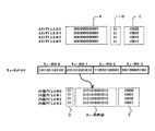
【図1】本発明の好ましい実施態様にかかるフラッシュメモリシステム1を概略的に示すブロック図である。
【図2】フラッシュメモリチップ2−0〜2−3を構成する各フラッシュメモリセル16の構造を概略的に示す断面図である。
【図3】書込状態であるフラッシュメモリセル16を概略的に示す断面図である。
【図4】フラッシュメモリチップ2−0のアドレス空間の構造を概略的に示す図である。
【図5】冗長領域26のデータ構造を概略的に示す図である。
【図6】仮想ブロックのマッピングの一例を示す図である。
【図7】図6に示された仮想ブロックの仮想ページ構造を示す図である。
【図8】アドレス変換テーブル31のデータ構造を示す概略図である。
【図9】消去済みブロックキュー32のデータ構造を示す概略図である。
【図10】読み出し動作1におけるアドレス変換テーブル31を用いた内部アドレスへの変換方法を説明するための図である。
【図11】読み出し動作2におけるアドレス変換テーブル31を用いた内部アドレスへの変換方法を説明するための図である。
【図12】書き込み動作1におけるアドレス変換テーブル31を用いた内部アドレスへの変換方法を説明するための図である。
【図13】書き込み動作1におけるフラッシュシーケンサブロック12による一連の書き込み動作タイミング概略的に示すタイミング図である。
【図14】書き込み動作2におけるアドレス変換テーブル31を用いた内部アドレスへの変換方法を説明するための図である。
【図15】書き込み動作2におけるフラッシュシーケンサブロック12による一連の書き込み動作タイミング概略的に示すタイミング図である。
【図16】書き込み動作3におけるフラッシュシーケンサブロック12による一連の書き込み動作タイミング概略的に示すタイミング図である。
【図17】書き込み動作4におけるアドレス変換テーブル31を用いた内部アドレスへの変換方法を説明するための図である。
【符号の説明】
1 フラッシュメモリシステム
2−0〜2−3 フラッシュメモリチップ
3 コントローラ
4 コネクタ
5 ホストコンピュータ
6 マイクロプロセッサ
7 ホストインターフェースブロック
8 SRAMワークエリア
9 バッファ
10 フラッシュメモリインターフェースブロック
11 ECCブロック
12 フラッシュシーケンサブロック
13〜15 バス
16 フラッシュメモリセル
17 P型半導体基板
18 ソース拡散領域
19 ドレイン拡散領域
20 トンネル酸化膜
21 フローティングゲート電極
22 絶縁膜
23 コントロールゲート電極
24 チャネル
25 ユーザ領域
26 冗長領域
27 エラーコレクションコード格納領域
28 仮想ブロックアドレス格納領域
31 アドレス変換テーブル
32 消去済みブロックキュー[0001]
BACKGROUND OF THE INVENTION
The present invention relates to a memory controller, a flash memory system, and a flash memory control method, and more particularly, to a memory controller, a flash memory system, and a flash memory control method capable of performing a series of data write processing on the flash memory at higher speed.
[0002]
[Prior art]
In recent years, flash memories, particularly NAND flash memories, are often used as semiconductor memories used for memory cards, silicon disks, and the like. In the NAND flash memory, when a memory cell is changed from an erased state (logical value = 1) to a written state (logical value = 0), this can be performed in units of memory cells. When changing from the write state (0) to the erase state (1), this cannot be performed in units of memory cells, but only in a predetermined erase unit (block unit) made up of a plurality of memory cells. I can't. Such a batch erase operation is generally called “block erase”.
[0003]
As described above, in the NAND flash memory, since the change from the write state (0) to the erase state (1) cannot be performed in units of memory cells, the data is written when data is written to the flash memory. It is necessary to erase all the memory cells included in the power region in advance. The block erased area becomes an empty block in which no data is stored, and when writing new data to the flash memory, such an empty block is searched and the relevant data is written to the found empty block. Will be. Here, each block is composed of a plurality of “pages” which are access units for reading and writing data.
[0004]
Such data writing to the flash memory is performed as follows.
[0005]
First, when a data write request is issued from the host computer and a write destination address and data to be written are transmitted, the data is temporarily stored in a memory provided in the controller. Next, the controller transfers the data temporarily stored in the memory to the flash memory and instructs the flash memory to write the data to the page indicated by the write destination address. In response to this, the flash memory stores the data transferred from the controller in the designated page, thereby completing a series of data write processing.
[0006]
[Problems to be solved by the invention]
Conventionally, each page in the same block is treated as having continuous addresses as viewed from the host computer. On the other hand, a data write request from the host computer is often made to a plurality of continuous addresses, and in this case, the controller needs to write data successively to a plurality of continuous pages in a certain block.
[0007]
In this case, the controller first transfers data to be written to the first page to the flash memory, and instructs the flash memory to write such data to the page. In response, when the flash memory stores the transferred data in the specified page, the controller then transfers the data to be written to the next page to the flash memory and writes the data to the page. To direct. By sequentially executing such processing for the requested plurality of addresses, a series of data writing processing to a plurality of continuous pages is completed.
[0008]
Here, the time required for the writing process for one page is mainly the time required for transferring the data to be written from the controller to the flash memory (data transfer time), and the time for issuing the write command from the controller to the flash memory. (Instruction issue time), time for actually writing data to the flash memory (flash program time), and the like. Of these, the flash program time requires a particularly long time (for example, about 200 μsec).
[0009]
Conventionally, such a single data writing process that requires a relatively long time is sequentially performed in units of pages. Therefore, when a host computer issues a data write request to a plurality of consecutive addresses, In order to complete the data writing process, a time substantially proportional to the number of pages to which data is to be written is required.
[0010]
Therefore, a memory controller, a flash memory system, and a flash memory control method that can perform a series of data write processing at a higher speed when a host computer requests data write to a plurality of consecutive addresses are desired. It was rare.
[0011]
Accordingly, an object of the present invention is to provide a memory controller capable of performing a series of data write processing on a flash memory at a higher speed, and a flash memory system including such a memory controller.
[0012]
Another object of the present invention is to provide a flash memory control method capable of performing a series of data write processing on the flash memory at a higher speed.
[0013]
[Means for Solving the Problems]
This object of the present invention is supplied from a host computer.Sector-by-sectorMultiple based on host addressIncludes pagePhysical blockMultiple erasures in unitsA memory controller for accessing flash memory,
Virtual block address assigning means for assigning a virtual block address to an area of a predetermined number of sectors in which the host address is continuous;
Virtual block management for managing a plurality of physical blocks selected from each flash memory one by one without depending on the same physical block address as a virtual block and managing the correspondence between the virtual block and the virtual block address Means,
Group dividing means for dividing the virtual block address into the virtual block address belonging to the first group and the virtual block address belonging to the second group;
In the case of the virtual block corresponding to the virtual block address belonging to the first group, in the physical block in which the consecutive host addresses are different for pages in a plurality of physical blocks included in the same virtual block In the case of the virtual block corresponding to the virtual block address belonging to the second group, the page in a plurality of physical blocks included in the same virtual block is allocated. Page management for allocating the host address so that consecutive host addresses are allocated to pages in the same physical blockMeans and
WithIt is characterized byAchieved by the memory controller.
The object of the present invention is also a memory controller for accessing a flash memory having a bank structure in which erasing is performed in units of physical blocks including a plurality of pages, based on a host address in units of sectors supplied from a host computer.
Virtual block address assigning means for assigning a virtual block address to an area of a predetermined number of sectors in which the host address is continuous;,
A virtual block that manages a plurality of physical blocks selected one by one as a virtual block without depending on the order of each bank in the bank, and manages the correspondence between the virtual block and the virtual block address Block management means;
Group dividing means for dividing the virtual block address into the virtual block address belonging to the first group and the virtual block address belonging to the second group;
In the case of the virtual block corresponding to the virtual block address belonging to the first group, in the physical block in which the consecutive host addresses are different for pages in a plurality of physical blocks included in the same virtual block In the case of the virtual block corresponding to the virtual block address belonging to the second group, the page in a plurality of physical blocks included in the same virtual block is allocated. In contrast, page management means for assigning the host address so that successive host addresses are assigned to pages in the same physical block;
This is achieved by a memory controller.
[0014]
According to the present invention, in the virtual block belonging to the first group, adjacent host addresses are assigned to different physical blocks in the virtual block, so access to a plurality of consecutive addresses is requested from the host computer. In this case, the physical blocks accessed by these addresses are different physical blocks. For this reason, each accessed physical block operates independently, whereby a series of processes can be performed in parallel. Thereby, a series of processes for the flash memory can be performed at higher speed. On the other hand, in the virtual block belonging to the second group, since adjacent host addresses are assigned to the same physical block in the virtual block, even if data overwriting is frequently instructed by the host computer Therefore, it is not necessary to transfer many physical blocks between blocks, and a series of data overwriting operations can be performed at high speed.
[0015]
In a preferred embodiment of the present invention, the virtual block belonging to the second group corresponds to an area including the head portion of the host address.
[0016]
According to the preferred embodiment of the present invention, overwriting of data stored in the head part of a host address such as FAT (file allocation table) can be performed at high speed.
[0017]
In a further preferred aspect of the present invention, the memory controller further comprises means for determining the number of virtual blocks belonging to the second group.
[0018]
According to a further preferred embodiment of the present invention, the number of virtual blocks belonging to the second group can be made variable.
[0019]
In a further preferred aspect of the present invention, the group classifies the plurality of physical blocks by at least a memory chip.
[0020]
According to a further preferred embodiment of the present invention, since the physical blocks are grouped by memory chip, the physical blocks corresponding to a plurality of consecutive host addresses in the virtual block belonging to the first group are different from each other. It belongs to the memory chip. For this reason, even if these memory chips are normal memory chips that cannot perform parallel processing, parallel processing can be performed by operating each memory chip independently.
[0021]
In a further preferred aspect of the present invention, the group classifies the plurality of physical blocks by at least banks.
[0022]
According to a further preferred embodiment of the present invention, since each physical block is grouped by bank, physical blocks corresponding to a plurality of consecutive host addresses in the virtual block belonging to the first group are different from each other. Will belong to. For this reason, even if there is only one memory chip, parallel processing can be performed because each bank operates independently. In particular, if a plurality of memory chips are used and a plurality of physical blocks belonging to different banks are virtually combined across a plurality of memory chips to form a virtual block, more processing is executed in parallel. Therefore, a series of processing for the flash memory can be performed at higher speed.
[0023]
The object of the present invention is also a memory controller for accessing a memory composed of a plurality of physical blocks each consisting of n physical pages based on a host address supplied from a host computer, wherein m physical Means for forming a virtual block consisting of n × m virtual pages by virtually combining the blocks, and for the virtual blocks belonging to the first group among the plurality of virtual blocks, a continuous host address is Means for allocating to successive virtual pages in the virtual block and assigning successive host addresses to successive physical pages in the virtual block for the virtual blocks belonging to the second group.
[0024]
In a preferred embodiment of the present invention, adjacent virtual pages in each virtual block belong to different physical blocks.
[0025]
In a further preferred aspect of the present invention, the virtual block belonging to the second group corresponds to an area including the head portion of the host address.
[0026]
The object of the invention is alsoA memory controller that accesses a plurality of flash memories to be erased in units of physical blocks including a plurality of pages based on a host address in units of sectors supplied from a host computer, wherein the predetermined sector in which the host addresses are continuous Virtual block address assigning means for assigning virtual block addresses to a number of areas, and managing a plurality of physical blocks selected one by one without depending on the difference of physical block addresses from each flash memory as virtual blocks, Virtual block management means for managing the correspondence between the virtual block and the virtual block address, and the virtual block address is divided into the virtual block address belonging to the first group and the virtual block address belonging to the second group Group dividing means, and belonging to the first group In the case of the virtual block corresponding to the virtual block address, the consecutive host addresses are assigned to pages in different physical blocks for pages in a plurality of physical blocks included in the same virtual block. In the case of the virtual block corresponding to the virtual block address belonging to the second group, the host address is allocated to the pages in a plurality of physical blocks included in the same virtual block. Page management means for allocating the host address so that the host address is allocated to a page in the same physical block.Memory controllerAnd equipped with multiple flash memoriesAchieved by flash memory system.
The object of the present invention is also a memory controller for accessing a flash memory having a bank structure in which erasing is performed in units of physical blocks including a plurality of pages, based on a host address in units of sectors supplied from a host computer. A plurality of virtual block address assigning means for assigning virtual block addresses to an area of a predetermined number of sectors in which the host address is continuous, and a plurality selected one by one without depending on the order in the bank. Virtual block management means for managing the physical block as a virtual block, managing the correspondence between the virtual block and the virtual block address, the virtual block address belonging to the first group and the second Group dividing means for dividing the virtual block address belonging to a group; In the case of the virtual block corresponding to the virtual block address belonging to the first group, in the physical block in which the consecutive host addresses are different with respect to the pages in the plurality of physical blocks included in the same virtual block In the case of the virtual block corresponding to the virtual block address belonging to the second group, the page in a plurality of physical blocks included in the same virtual block is allocated. In contrast, the memory controller includes a page management unit that allocates the host address so that the consecutive host addresses are allocated to pages in the same physical block, and a flash memory having a bank structure. Achieved by flash memory system.
[0027]
The object of the invention is alsoA flash memory control method for controlling a plurality of flash memories to be erased in units of physical blocks including a plurality of pages based on a sector-unit host address supplied from a host computer,
A virtual block address is assigned to an area of a predetermined number of sectors in which the host address is continuous,
A plurality of physical blocks selected one by one without depending on the difference of physical block addresses from each flash memory are set as virtual blocks, and the correspondence between the virtual blocks and the virtual block addresses is managed,
Dividing the virtual block address into the virtual block address belonging to the first group and the virtual block address belonging to the second group;
In the case of the virtual block corresponding to the virtual block address belonging to the first group, in the physical block in which the consecutive host addresses are different for pages in a plurality of physical blocks included in the same virtual block In the case of the virtual block corresponding to the virtual block address belonging to the second group, the page in a plurality of physical blocks included in the same virtual block is allocated. The host addresses are allocated so that consecutive host addresses are allocated to pages in the same physical block.This is achieved by a method for controlling a flash memory.
The object of the present invention is also a flash memory control method for controlling a bank-structured flash memory in which erasure is performed in units of physical blocks including a plurality of pages based on a sector-unit host address supplied from a host computer. There,
A virtual block address is assigned to an area of a predetermined number of sectors in which the host address is continuous,
A plurality of physical blocks selected one by one without depending on the difference in order in each bank from each bank are set as virtual blocks, and the correspondence between the virtual blocks and the virtual block addresses is managed,
Dividing the virtual block address into the virtual block address belonging to the first group and the virtual block address belonging to the second group;
In the case of the virtual block corresponding to the virtual block address belonging to the first group, in the physical block in which the consecutive host addresses are different for pages in a plurality of physical blocks included in the same virtual block In the case of the virtual block corresponding to the virtual block address belonging to the second group, the page in a plurality of physical blocks included in the same virtual block is allocated. On the other hand, it is achieved by a flash memory control method for allocating the host address so that consecutive host addresses are allocated to pages in the same physical block.
[0028]
Preferred Embodiment of the Invention
Hereinafter, preferred embodiments of the present invention will be described in detail with reference to the accompanying drawings.
[0029]
FIG. 1 is a block diagram schematically showing a
[0030]
As shown in FIG. 1, the
[0031]
Each of the flash memory chips 2-0 to 2-3 is a semiconductor chip having a storage capacity of 128 Mbytes (1 Gbit). In the
[0032]
The controller 3 includes a microprocessor 6, a host interface block 7, an
[0033]
The microprocessor 6 is a functional block for controlling the operation of the entire functional blocks constituting the controller 3.
[0034]
The host interface block 7 is connected to the connector 4 via the
[0035]
The
[0036]
The buffer 9 is a buffer for temporarily storing data read from the flash memory chips 2-0 to 2-3 and data to be written to the flash memory chips 2-0 to 2-3. That is, data read from the flash memory chips 2-0 to 2-3 is held in the buffer 9 until the
[0037]
The flash
[0038]
The
[0039]
The
[0040]
Next, a specific structure of each flash memory cell constituting each flash memory chip 2-0 to 2-3 will be described.
[0041]
FIG. 2 is a cross-sectional view schematically showing the structure of each
[0042]
As shown in FIG. 2, the
[0043]
The
[0044]
As shown in FIG. 2, the erased state refers to a state where electrons are not injected into the floating
[0045]
FIG. 3 is a cross-sectional view schematically showing the
[0046]
As shown in FIG. 3, the writing state refers to a state in which electrons are accumulated in the floating
[0047]
Here, whether the selected
[0048]
When the
[0049]
Next, a specific configuration of the address space of each flash memory chip 2-0 to 2-3 will be described.
[0050]
FIG. 4 is a diagram schematically showing the structure of the address space of the flash memory chip 2-0.
[0051]
As shown in FIG. 4, the address space of the flash memory chip 2-0 is configured by 8192 physical blocks including
[0052]
Here, each physical block is a data erasing unit. That is, in the flash memory chips 2-0 to 2-3, the state of each
[0053]
Further, as shown in FIG. 4, each of the
[0054]
Each of these pages is an access unit for reading and writing data. As shown in FIG. 4, 8 bits consisting of bits b0 to b7 are defined as 1 byte, and a
[0055]
FIG. 5 is a diagram schematically showing the data structure of the
[0056]
As shown in FIG. 5, the
[0057]
The error collection
[0058]
The virtual block
[0059]
The other areas of the
[0060]
Thus, each page is composed of a 512-
[0061]
As described above, each of the flash memory chips 2-0 to 2-3 is composed of 8192 physical blocks. Of these, 8000 physical blocks are blocks that can actually store data (hereinafter referred to as “blocks”). The remaining 192 blocks are treated as “redundant blocks”. The redundant block is an empty block waiting for data writing. The address space of the flash memory chips 2-0 to 2-3 is composed only of actual use blocks. Further, when a defect occurs in a certain physical block and becomes unusable, the number of physical blocks allocated as redundant blocks is reduced by the number of blocks in which the defect has occurred.
[0062]
Further, the actual use block constitutes a “virtual block” in which four physical blocks selected one by one from each of the flash memory chips 2-0 to 2-3 are virtually combined. As a result, a maximum of 8000 virtual blocks including
[0063]
FIG. 6 is a diagram illustrating an example of virtual block mapping.
[0064]
In the example shown in FIG. 6, the physical block # 150 included in the flash memory chip 2-0, the physical block # 6811 included in the flash memory chip 2-1, the physical block # 8191 included in the flash memory chip 2-2, Physical blocks # 3048 included in the flash memory chip 2-3 are virtually combined to form one virtual block. Thus, in this embodiment, it is necessary that the four physical blocks constituting one virtual block are included in different flash memory chips. In this way, a maximum of 8000 virtual blocks are configured.
[0065]
FIG. 7 is a diagram showing a virtual page structure of the virtual block shown in FIG.
[0066]
As illustrated in FIG. 7, the virtual block is handled as one block configured by 128 virtual pages including
[0067]
Next, the relationship between the virtual block and the four physical blocks that constitute it will be described.
[0068]
As described above, in this embodiment, a maximum of 8000 virtual blocks are configured by 8192 physical blocks included in each of the flash memory chips 2-0 to 2-3. The relationship with the four physical blocks constituting each virtual block is held in the address conversion table 31 developed on the
[0069]
FIG. 8 is a schematic diagram showing the data structure of the address conversion table 31.
[0070]
As shown in FIG. 8, the address conversion table 31 includes 8000 virtual block display areas including virtual block
[0071]
In cells # j-0 to # j-3 included in each virtual block display area, the addresses (physical block addresses) of the physical blocks constituting the virtual block are stored. Here, the “physical block address” is an address representing a block number assigned to each physical block in binary, and is composed of 13 bits. For example, if the virtual block shown in FIGS. 6 and 7 is
[0072]
Also, flag # j-0 to flag # j-3 included in each virtual block indicate whether the content stored in the cell is valid or invalid. Specifically, the content of the corresponding cell is valid if the flag indicates “1”, and the content of the corresponding cell is invalid if the flag indicates “0”. Therefore, the content of the cell whose corresponding flag indicates “0” is ignored.
[0073]
Of the 8000 virtual block display areas constituting the address conversion table 31, virtual block
[0074]
As described above, the address conversion table 31 includes 32000 cells and 32000 flags. Each cell stores 13-bit information (physical block address), and each flag stores 1-bit information. Therefore, the address conversion table 31 occupies about 64 kbytes of the storage capacity of the
[0075]
The address conversion table 31 is generated as follows.
[0076]
Of the physical blocks constituting the flash memory chips 2-0 to 2-3, the virtual block
[0077]
Here, in the erased empty block, the virtual block address stored in the virtual block
[0078]
Therefore, the microprocessor 6 refers to the virtual block address included in the
[0079]
Such processing is performed for all physical blocks in which data is stored. Thereby, the generation of the address conversion table 31 is completed.
[0080]
Next, the data structure of the erased
[0081]
FIG. 9 is a schematic diagram showing the data structure of the erased
[0082]
As shown in FIG. 9, the erased
[0083]
In queues # k-0 to # k-3 constituting each
[0084]
In this manner, the physical block addresses of up to six erased blocks are registered in the erased
[0085]
The generation of the erased
[0086]
Next, the operation of the
[0087]
First, a data read operation by the
[0088]
In the data read operation, after the conversion from the host address to the internal address is performed, the user data is read using the internal address.Whether the virtual block to be accessed is a horizontal writing virtual block, The address conversion method varies depending on whether the virtual block is vertically written. Hereinafter, the access target virtual block is divided into a horizontal writing virtual block and a vertical writing virtual block, which will be described in detail with specific examples.
[0089]
Read operation 1 (when reading data from horizontal writing virtual block)
In this example, a host address, for example, “0000011111111110000000B” is supplied to the
[0090]
First, when a host address and an external read command are supplied to the controller 3, the host address and the external read command are temporarily stored in a task file register (not shown) included in the host interface block 7.
[0091]
Next, whether or not the host address stored in the task file register (not shown) is a correct address, that is, whether or not the host address indicates a physical address that does not originally exist or an invalid address. This is determined by the host interface block 7.
[0092]
As a result of the determination, if it is determined that the host address stored in the task file register (not shown) is a valid address, it is converted into an internal address using the address conversion table 31. On the other hand, if it is determined that this is an abnormal address, an error register (not shown) included in the host interface block 7 is set, and the host computer knows that an error has occurred by referring to the contents of the register. be able to.
[0093]
Next, conversion to an internal address using the address conversion table 31 when the virtual block to be accessed is a horizontal writing virtual block will be described with reference to FIG.
[0094]
In FIG. 10, for convenience, the upper 13 bits from the host address are represented as “A”, the upper 14 bits to the upper 18 bits are represented as “B”, and the lower 2 bits are represented as “C”. .
[0095]
First, under the control of the microprocessor 6, the upper 13 bits (A) are extracted from the 20-bit host address, and any virtual block display area in the address conversion table 31 is selected. In this example, since the upper 13 bits (A) of the host address are “00000111111111B (255)”, the selected virtual block display area is the virtual block
[0096]
If it is determined that the virtual block to be accessed is a horizontal writing virtual block, then, under the control of the microprocessor 6, the four cells and the four cells included in the selected virtual block
[0097]
Next, under the control of the microprocessor 6, the lower 2 bits (C) of the host address, the contents of the read cell, and the 5 bits (B) consisting of the upper 14th bit to the upper 18th bit of the host address Are combined in this order. The combined address becomes an internal address. In this case, the lower 2 bits (C) of the host address are “00B”, the content of the read cell is “0000100001111B”, and the 5 bits (the upper 14th bit to the upper 18th bit of the host address) Since B) is “11000B”, the obtained internal address is “00000010000111111000B” as shown in FIG.
[0098]
Thus, the conversion from the host address to the internal address is completed.
[0099]
On the other hand, in response to the external read command being stored in a task file register (not shown) of the host interface block 7, a register (not shown) of the
[0100]
First, an internal read command, which is a kind of internal command, is set in a predetermined register (not shown) in the
[0101]
When the settings for the various registers included in the
[0102]
First, the
[0103]
Next, the
[0104]
In response to this, the flash memory chip 2-0 executes the reading of the data stored in the supplied 18-bit internal address “000010000111111000B”. Here, in the supplied 18-bit internal address “000010000111111000B”, the upper 13 bits specify a physical block, and the lower 5 bits are used to specify a physical page in the physical block. In this case, since the upper 13 bits are “0000100001111B (271)” and the lower 5 bits are “11000B (24)”, the specified physical block is block # 271 and the specified physical page is physical page #. 24. In other words, the flash memory chip 2-0 executes reading of data stored in the
[0105]
As described with reference to FIG. 7, in this embodiment, four physical blocks are virtually combined to form one virtual block, and therefore, physical block # 271 belonging to the flash memory chip 2-0.
[0106]
The user data and additional information read from the flash memory chip 2-0 in this way are supplied to the flash
[0107]
The user data stored in the buffer 9 is supplied from the host interface block 7 to the
[0108]
Thus, a series of read operations is completed.
[0109]
Thus, when the virtual block to be accessed is a horizontal writing virtual block, the lower 2 bits (C) of the host address are assigned to the upper 2 bits of the internal address, and the upper 14th bit to the upper 18 of the host address. Since the 5 bits (B) consisting of the bit are assigned to the lower 5 bits of the internal address, the lower 7 bits “0000000B” to “1111111B” of the host address are respectively
[0110]
Next, a read operation when the virtual block to be accessed is a vertically written virtual block will be described.
[0111]
Read operation 2 (when reading data from a vertically written virtual block)
In this example, a host address such as “0000000000000010101101B” is supplied to the
[0112]
First, when a host address and an external read command are supplied to the controller 3, as described above, whether or not the host address is a valid address is determined by the host interface block 7, and as a result, this is valid. If the address is determined, it is converted into an internal address using the address conversion table 31.
[0113]
Next, conversion to an internal address using the address conversion table 31 when the virtual block to be accessed is a vertically written virtual block will be described with reference to FIG.
[0114]
In FIG. 11, for convenience, the upper 13 bits from the host address are represented as “A”, the upper 14 bits and the upper 15 bits are represented as “D”, and the lower 5 bits are represented as “E”. .
[0115]
First, under the control of the microprocessor 6, the upper 13 bits (A) are extracted from the 20-bit host address, and any virtual block display area in the address conversion table 31 is selected. In this example, since the upper 13 bits (A) of the host address are “0000000000000000 (0)”, the selected virtual block display area is the virtual block
[0116]
If it is determined that the virtual block to be accessed is a vertically written virtual block, then, under the control of the microprocessor 6, the four cells and the four cells included in the selected virtual block
[0117]
Next, under the control of the microprocessor 6, 2 bits (D) consisting of the upper 14 bits and the upper 15 bits of the host address, the contents of the read cell, and the lower 5 bits (E) of the host address Are combined in this order. The combined address becomes an internal address. In this case, 2 bits (D) consisting of the upper 14 bits and the upper 15 bits of the host address are “10B”, the content of the read cell is “1110000000000000”, and the lower 5 bits ( Since E) is “10101B”, the obtained internal address is “10111000000000010101B” as shown in FIG.
[0118]
Thus, the conversion from the host address to the internal address is completed.
[0119]
As described above, when the virtual block to be accessed is a vertically written virtual block, the conversion to the internal address is performed by a method different from that in the case where the virtual block to be accessed is a horizontally written virtual block.
[0120]
When the conversion from the host address to the internal address is completed in this way, the same operation as the
[0121]
As described with reference to FIG. 7, in this embodiment, since four physical blocks are virtually combined to form one virtual block, physical block # 7168 belonging to the flash memory chip 2-2. The
[0122]
The user data and additional information read from the flash memory chip 2-2 in this way are supplied to the
[0123]
Thus, a series of read operations is completed.
[0124]
Thus, when the virtual block to be accessed is a vertically written virtual block, 2 bits (D) consisting of the upper 14 bits and the upper 15 bits of the host address are assigned to the upper 2 bits of the internal address. Since the lower 5 bits (E) of the host address are assigned to the lower 5 bits of the internal address, the consecutive lower 7 bits “0000000B” to “0011111B” of the host address are the physical blocks constituting the virtual block. , Corresponding to the
[0125]
The significance of different address conversion methods depending on whether the virtual block to be accessed is a vertical writing virtual block or a horizontal writing virtual block is described below. It will become clear in the explanation of.
[0126]
Next, various data write operations by the
[0127]
In the data write operation, when the virtual block to be accessed is a horizontal writing virtual block and when it is a vertical writing virtual block, the operation is different, and there is no virtual block to be accessed (new data is written) Operation) and when the virtual block to be accessed already exists (when data is overwritten). Therefore, each case will be described.
[0128]
Write operation 1 (when writing data to an empty block (when the host address corresponds to a horizontal writing virtual block))
When data is written to an empty block, that is, when a host address corresponds to a horizontal write virtual block in a new data write operation, a virtual block is generated and redundant data for
[0129]
Here, from the
[0130]
First, when the host addresses # 0 to # 3 and the external write command are supplied to the controller 3, the host addresses # 0 to # 3 and the external write command are stored in a task file register (not shown) included in the host interface block 7. Temporarily stored. Further, when write data corresponding to the host addresses # 0 to # 3 is supplied to the controller 3, these data are sent to the
[0131]
Next, whether or not the host addresses # 0 to # 3 stored in the task file register (not shown) are correct addresses, that is, the host addresses # 0 to # 3 are originally nonexistent physical addresses or invalid. The host interface block 7 determines whether or not a correct address is indicated.
[0132]
As a result of the determination, if it is determined that the host addresses # 0 to # 3 stored in the task file register (not shown) are valid addresses, they are converted into internal addresses using the address conversion table 31. On the other hand, if it is determined that this is an abnormal address, an error register (not shown) included in the host interface block 7 is set, and the host computer knows that an error has occurred by referring to the contents of the register. be able to.
[0133]
FIG. 12 is a diagram for explaining a conversion method to an internal address using the address conversion table 31 when a virtual block to be accessed is a horizontal writing virtual block.
[0134]
As shown in FIG. 12, in this example, since the upper 13 bits (A) of the host addresses # 0 to # 3 are “0001010101010B (682)”, the selected virtual block display area is the virtual block display area. # 682. At this time, it is determined that the virtual block to be accessed is a horizontal writing virtual block.
[0135]
If it is determined that the virtual block to be accessed is a horizontal writing virtual block, then, under the control of the microprocessor 6, from the address conversion table 31 stored in the
[0136]
Next, under the control of the microprocessor 6, any one of the queue sets # 0 to # 5 constituting the erased
[0137]
When the contents stored in the queues # 0-0 to # 0-3 are read, these are stored in the cell # 682-0 to the cell # 682-3 of the virtual block display area # 682, and the corresponding flag # All of 682-0 to # 682-3 are rewritten to “1 (valid)”. Thereby, the generation of the virtual block is completed.
[0138]
Then, as shown in FIG. 12, under the control of the microprocessor 6, the lower 2 bits (C) of the host addresses # 0 to # 3, the contents of the corresponding queue, and the host addresses # 0 to # 3 The 5 bits (B) consisting of the upper 14 bits to the upper 18 bits are combined in this order. The combined addresses are
[0139]
Thereby, the conversion from the host addresses # 0 to # 3 to the
[0140]
Further, in response to the external write command being stored in a task file register (not shown) of the host interface block 7, a register (not shown) of the
[0141]
First, under the control of the microprocessor 6, a data transfer command and an internal write command, which are a kind of internal commands, are set in predetermined registers (not shown) in the
[0142]
When the setting for various registers (not shown) included in the
[0143]
FIG. 13 is a timing chart schematically showing a series of write operations to the
[0144]
First, the
[0145]
Next, based on the upper 2 bits of the
[0146]
Next, the
[0147]
As a result, the flash memory chip 2-0 is allowed to accept data to be written in the page corresponding to the lower 18 bits “000000000111100000B” of the supplied
[0148]
Next, data to be written to the
[0149]
The virtual block address supplied to the
[0150]
In this way, when additional information such as a virtual block address is transferred to the flash memory chip 2-0 that is permitted to accept write data, the additional information is stored in the flash memory chip 2-0. Is temporarily stored in a register (not shown).
[0151]
Next, the
[0152]
In response to this, the flash memory chip 2-0 writes the additional information stored in the predetermined register to the address designated by the transfer destination designation processing (flash programming). In other words, the additional information stored in the register is written to the page specified by the lower 18 bits “000000000111100000B” of the
[0153]
While the flash memory chip 2-0 is executing flash programming, the
[0154]
Such a write operation is also performed for the virtual page # 2 and the virtual page # 3 of the virtual block # 682 using the internal addresses # 7 and # 8, thereby the
[0155]
When a series of writing processes for the
[0156]
A series of write operations to the virtual pages # 68 to # 71 of the virtual block # 682 by the
[0157]
First, the
[0158]
Next, the
[0159]
As a result, the flash memory chip 2-0 is allowed to accept data to be written in the page corresponding to the lower 18 bits “000000000111110001B” of the supplied
[0160]
Next, of the write data stored in the buffer 9, additional information to be stored in the
[0161]
In this way, when additional information such as write data and an error correction code is transferred to the flash memory chip 2-0 that is permitted to accept write data, the write data and error correction code are The data is temporarily stored in a register (not shown) provided in the flash memory chip 2-0.
[0162]
Next, the
[0163]
In response to this, the flash memory chip 2-0 writes additional information such as data stored in a predetermined register and an error correction code to an address designated by the transfer destination designation processing (flash programming). That is, the additional information such as the data stored in the register and the error correction code is specified by the lower 18 bits “000000000111110001B” of the
[0164]
While the flash memory chip 2-0 is executing the flash programming, the
[0165]
Next, the
[0166]
Thereafter, as described above, a data transfer and a write command are issued to the flash memory chip 2-1, and additional information such as data corresponding to the
[0167]
Such a data write operation is also performed for the internal addresses # 2 and # 3, whereby the data corresponding to the host addresses # 2 and # 3 and the additional information such as the corresponding error correction code are also internally stored. Write to the page specified by addresses # 2 and # 3. In this case, since the lower 18 bits of the internal address # 2 are “010111111000000010001B”, the additional information such as the data corresponding to the host address # 2 and the corresponding error correction code is the physical block # 3056 of the flash memory chip 2-2. Is written to the
[0168]
Here, the
[0169]
Further, in response to the fact that the physical block address stored in the
[0170]
In this way, a series of write operations by the
[0171]
In such a series of write operations, it is important that data corresponding to successive host addresses # 0 to # 3 is written in different physical blocks belonging to different flash memory chips 2-0 to 2-3, respectively. . These four physical blocks constitute one virtual block # 682 as described above, and the data corresponding to the continuous host addresses # 0 to # 3 are the continuous virtual pages # 68 to ## in the virtual block # 682. 71 is written.
[0172]
In the above example, the virtual block address is also written to pages (virtual pages # 68 to # 71) other than the
[0173]
Write operation 2 (when writing data to an empty block (when the host address corresponds to a vertically written virtual block))
When writing data to an empty block, that is, when the host address corresponds to a vertically written virtual block in a new data write operation, a partial virtual block is generated, and a virtual block is generated from
[0174]
Here, from the
[0175]
First, when host addresses # 0 to # 3, write data corresponding to these, and external write commands are supplied to the controller 3, as described above, it is determined whether or not the host address is a valid address. The error correction code corresponding to the writing is generated by the
[0176]
FIG. 14 is a diagram for explaining a conversion method to an internal address using the address conversion table 31 when the virtual block to be accessed is a vertically written virtual block.
[0177]
As shown in FIG. 14, in this example, the upper 13 bits (A) of the host addresses # 0 to # 3 are “0000000000001B (1)”, and the upper 14th bit and the upper bits of the host addresses # 0 to # 3. Since the two bits (D) consisting of the 15th bit are “01B (1)”, the selected cell and flag are the cell # 1-1 and the flag # 1-1 in the virtual block
[0178]
If it is determined that the virtual block to be accessed is a vertically written virtual block, then
[0179]
Next, under the control of the microprocessor 6, the erased
[0180]
When the contents stored in the queue # 0-1 are read, this is stored in the cell # 1-1 of the virtual block
[0181]
Then, as shown in FIG. 14, under the control of the microprocessor 6, 2 bits (D) consisting of the upper 14 bits and the upper 15 bits of the host addresses # 0 to # 3, the contents of the corresponding queue and The lower 5 bits (E) of the host addresses # 0 to # 3 are combined in this order. The combined addresses are
[0182]
Thereby, the conversion from the host addresses # 0 to # 3 to the
[0183]
Further, in response to the external write command being stored in a task file register (not shown) of the host interface block 7, a register (not shown) of the
[0184]
First, under the control of the microprocessor 6, a data transfer command and an internal write command, which are a kind of internal commands, are set in predetermined registers (not shown) in the
[0185]
When the setting for various registers (not shown) included in the
[0186]
FIG. 15 is a timing chart schematically showing a series of write operations to the
[0187]
First, the
[0188]
Next, based on the upper 2 bits of the
[0189]
Next, the
[0190]
As a result, the flash memory chip 2-1 is allowed to accept data to be written in the page corresponding to the lower 18 bits “0101010101101000000B” of the supplied
[0191]
Next, data to be written to the
[0192]
The virtual block address supplied to the
[0193]
In this way, when additional information such as a virtual block address is transferred to the flash memory chip 2-1 that is permitted to accept write data, the additional information is stored in the flash memory chip 2-1. Is temporarily stored in a register (not shown).
[0194]
Next, the
[0195]
In response to this, the flash memory chip 2-1 writes the additional information stored in a predetermined register at the address designated by the transfer destination designation process (flash programming). That is, the additional information stored in the register is written to the page specified by the lower 18 bits “0101010101101000000B” of the
[0196]
While the flash programming is being executed, the flash memory chip 2-1 is in a busy state, and the next write operation cannot be performed.
[0197]
When the flash programming is completed and the busy state is released, the user data and various redundant data are written to the virtual pages # 65, # 69, # 73, and # 77 of the
[0198]
In this way, a series of write operations by the
[0199]
Further, in response to the fact that the physical block address stored in the queue # 0-1 of the erased
[0200]
As described above, in the write operation 2, unlike the above-described
[0201]
In the above example, the virtual block address is also written in pages (physical pages # 16 to # 19) other than the first page (physical page # 0) of the physical block. I do not care.
[0202]
Write operation 3 (when data is overwritten in a virtual block (when the host address corresponds to a horizontal write virtual block))
When data is added and written to a virtual block (used block) in which data is already stored, “inter-block transfer” is performed.
[0203]
Here, transfer between blocks will be described.
[0204]
As described above, the
[0205]
Therefore, when overwriting old data stored in a physical page with new data, in order to prevent data stored in other physical pages included in the physical block to which this physical page belongs, This is because a process of moving data stored in another physical page to another physical block is necessary.
[0206]
This data movement accompanying the overwriting process is called “inter-block transfer”. In this specification, the physical block address of the transfer source physical block is referred to as “transfer source block address”, and the physical block address of the transfer destination physical block is referred to as “transfer destination block address”.
[0207]
The data overwriting operation when the virtual block to be accessed is a horizontal writing virtual block will be described below.
[0208]
Here, in a state immediately after the above-described
[0209]
First, when the host addresses # 0 to # 3 and the external write command are supplied to the controller 3, the host addresses # 0 to # 3 and the external write command are stored in a task file register (not shown) included in the host interface block 7. Temporarily stored. Further, when write data corresponding to the host addresses # 0 to # 3 is supplied to the controller 3, these data are sent to the
[0210]
Next, the transfer source block address and the transfer destination block address are generated using the address conversion table 31.
[0211]
FIG. 16 is a diagram for explaining a method of generating a transfer source block address and a transfer destination block address.
[0212]
As shown in FIG. 16, in this example, since the upper 13 bits (A) of the host addresses # 0 to # 3 are “0001010101010B”, the selected virtual block is the virtual block # 682. At this time, it is determined that the virtual block to be accessed is a horizontal writing virtual block.
[0213]
If it is determined that the virtual block to be accessed is a horizontal writing virtual block, the virtual block display area # 682 is then retrieved from the address conversion table 31 stored in the
[0214]
When the contents stored in the cells # 682-0 to # 682-3 are read, a transfer source block address is generated using the contents under the control of the microprocessor 6.
[0215]
The transfer source block address is generated by combining the lower two bits (C) of the host addresses # 0 to # 3 and the contents of the read cells in this order under the control of the microprocessor 6. In this case, the lower two bits (C) of the host addresses # 0 to # 3 are “00B” to “11B”, respectively, and the contents of the read cells are “0000000001111B”, “1110000110011B”, “01011111110000B”, “ Therefore, the values of the obtained four transfer source block addresses # 0 to # 3 are the values shown in FIG.
[0216]
Thereby, the generation of the transfer source block addresses # 0 to # 3 is completed.
[0217]
Next, under the control of the microprocessor 6, one of the queue sets # 0 to # 5 constituting the erased
[0218]
When the contents stored in the queues # 1-0 to # 1-3 are read, the cells # 682-0 constituting the virtual block display area # 682 of the address translation table 31 under the control of the microprocessor 6 are read out. -# 682-3 are overwritten and a transfer destination block address is generated using these.
[0219]
The transfer destination block address is generated by combining the lower 2 bits (C) of the host addresses # 0 to # 3 and the contents of the read queue in this order under the control of the microprocessor 6. In this case, the lower 2 bits (C) of the host addresses # 0 to # 3 are “00B” to “11B”, respectively, and the contents of the read queues are “00110000100000B”, “1000000000100B”, “01111101000B”, “ Therefore, the values of the four transfer destination block addresses # 0 to # 3 obtained are the values shown in FIG.
[0220]
Thereby, the generation of the transfer destination block addresses # 0 to # 3 is completed.
[0221]
When the above processing is completed, settings are made for a register (not shown) of the
[0222]
First, under the control of the microprocessor 6, a data transfer command, an internal write command, and an internal read command are set in predetermined registers (not shown) in the
[0223]
When the setting for various registers (not shown) included in the
[0224]
First, the
[0225]
Next, the
[0226]
As a result, the flash memory chip 2-0 reads the data stored in the lower 18 bits “000000000111100000B” of the supplied transfer source internal address. In other words, the flash memory chip 2-0 executes reading of data stored in the
[0227]
The data read from the flash memory chip 2-0 in this way is supplied to the flash
[0228]
Such a read operation is also performed on the flash memory chips 2-1 to 2-3 by adding “00000B (0)” to the transfer source block addresses # 1 to # 3. Data stored in
[0229]
Next, a data write operation temporarily stored in the buffer 9 is performed. Such a write operation is performed at the timing shown in FIG.
[0230]
First, the
[0231]
Next, the
[0232]
Next, the
[0233]
Next, of the data stored in the buffer 9, the additional information to be stored in the
[0234]
Next, the
[0235]
In response to this, the flash memory chip 2-0 writes additional information such as data stored in a predetermined register and an error correction code to an address designated by the transfer destination designation processing (flash programming). That is, the data stored in the register and the additional information such as the error correction code are pages of the transfer destination internal address specified by the lower 18 bits “0010000001000000B”, that is, the physical block # 1040 of the flash memory chip 2-0. It is written to
[0236]
While the flash memory chip 2-0 is executing the flash programming, the
[0237]
Next, the
[0238]
Next, of the data stored in the buffer 9, the additional information to be stored in the
[0239]
Such a writing process is also performed on the flash memory chips 2-2 and 2-3 by adding “00000B (0)” to the transfer destination block addresses # 2 and # 3. The additional information to be stored in the
[0240]
As a result, the data stored in the
[0241]
Such data transfer operation is successively performed by incrementing a 5-bit value added to the transfer source block address and the transfer destination block address. That is, if the 5-bit value added to the transfer source block address and the transfer destination block address is “00001 (1)”, the virtual pages # 4 to # 7 of the transfer source virtual block are transferred to the transfer destination virtual block. If the data is transferred to the virtual pages # 4 to # 7 and “00010 (2)”, the
[0242]
Such a transfer operation is continuously performed until the added 5-bit value coincides with “10000B (16)” which is 5 bits (B) including the upper 14th bit to the upper 18th bit of the host address. Done. That is, as a result of incrementing the 5 bits to be added, this becomes “10000B (16)”, and when it matches the 5 bits (B) consisting of the upper 14 bits to the upper 18 bits of the host address, the transfer described above is once performed. Operation is interrupted. In this example, when the data transfer from the
[0243]
When the added 5 bits match the 5 bits (B) consisting of the upper 14 bits to the upper 18 bits of the host address, the
[0244]
Next, the
[0245]
Next, additional information such as write data corresponding to the
[0246]
Next, the
[0247]
In this way, while the flash memory chip 2-0 is performing flash programming of additional information such as write data corresponding to the
[0248]
As a result, the write data corresponding to the host addresses # 0 to # 3 are written in the virtual pages # 64 to # 67 of the transfer destination virtual block, respectively.
[0249]
When the data writing is completed, 5 bits added to the transfer source block address and the transfer destination block address are incremented again, and the data transfer using the new transfer source internal address and transfer destination internal address is resumed. Such a transfer operation is continuously performed until the data transfer when the added 5 bits are “11111 (31)” is completed. That is, the process is performed until the data transfer from the virtual pages # 68 to # 127 of the transfer source virtual block to the virtual pages # 68 to # 127 of the transfer destination virtual block is completed. The data transfer operation is completed.
[0250]
Further, in response to the fact that the physical block address stored in the
[0251]
Note that each of the transfer-source physical blocks is erased as a block, thereby becoming a new erased block. Even in such block erasure, since each physical block of the transfer source belongs to a different flash memory chip, block erasure operations for these blocks can be executed in parallel.
[0252]
Thus, a series of block transfer operations is completed.
[0253]
As described above, when data is overwritten when the virtual block to be accessed is a horizontal writing virtual block, inter-block transfer is performed to four physical blocks, but these inter-block transfers are executed in parallel. For this reason, the time required for a series of inter-block transfer operations is significantly shortened as compared with the case where these are performed independently.
[0254]
Write operation 4 (when data is overwritten in a virtual block (when the host address corresponds to a vertically written virtual block))
As described above, the vertical writing virtual block corresponds to the area including the head part of the host address and generally stores FAT (file allocation table) or the like. In many cases, writing frequently occurs in smaller sector units (page units) than in horizontal writing virtual blocks. For this reason, in the data overwriting operation when the host address corresponds to the vertical writing virtual block, as will be described in detail below, inter-block transfer is performed for only one physical block. A series of operation times required is shortened.
[0255]
Here, in a state immediately after the above-described write operation 2 is completed, an external write command that is a kind of external command and four host addresses “00000000000010101000B” from the
[0256]
First, when the host addresses # 0 to # 3 and the external write command are supplied to the controller 3, as described above, the
[0257]
Next, the transfer source block address and the transfer destination block address are generated using the address conversion table 31.
[0258]
FIG. 17 is a diagram for explaining a method of generating a transfer source block address and a transfer destination block address.
[0259]
As shown in FIG. 17, in this example, since the upper 13 bits (A) of the host addresses # 0 to # 3 are “0000000000001B”, the selected virtual block is the
[0260]
If it is determined that the virtual block to be accessed is a vertically written virtual block, then
[0261]
When the contents stored in the cell # 1-1 are read, a transfer source block address is generated using the content under the control of the microprocessor 6.
[0262]
Under the control of the microprocessor 6, the transfer source block address is 2 bits (D) consisting of the upper 14 bits and the upper 15 bits of the host addresses # 0 to # 3, and the contents of the read cells are in this order. Generated by combining. In this case, 2 bits (D) consisting of the upper 14th bit and the upper 15th bit of the host addresses # 0 to # 3 are “01B”, and the content of the read cell is “0101010101010B”. The value of the obtained transfer source block address is the value shown in FIG.
[0263]
Thereby, the generation of the transfer source block address is completed.
[0264]
Next, under the control of the microprocessor 6, one of the queue sets # 0 to # 5 constituting the erased
[0265]
When the contents stored in the queue # 1-1 are read out, they are overwritten on the cell # 1-1 constituting the virtual block
[0266]
Under the control of the microprocessor 6, the transfer destination block address is 2 bits (D) consisting of the upper 14 bits and the upper 15 bits of the host addresses # 0 to # 3, and the contents of the read queue are in this order. Generated by combining. In this case, 2 bits (D) consisting of the upper 14 bits and the upper 15 bits of the host addresses # 0 to # 3 are “01B”, and the content of the read cell is “1011100110011B”. The value of the transfer destination block address obtained is the value shown in FIG.
[0267]
Thereby, the generation of the transfer destination block address is completed.
[0268]
When the above processing is completed, settings are made for a register (not shown) of the
[0269]
First, under the control of the microprocessor 6, a data transfer command, an internal write command, and an internal read command are set in predetermined registers (not shown) in the
[0270]
When the setting for various registers (not shown) included in the
[0271]
First, the
[0272]
Next, the
[0273]
As a result, the flash memory chip 2-1 reads the data stored in the lower 18 bits “0101010101101000000B” of the supplied transfer source internal address. That is, the flash memory chip 2-1 executes reading of data stored in the
[0274]
The data read from the flash memory chip 2-1 in this way is supplied to the flash
[0275]
Next, a data write operation temporarily stored in the buffer 9 is performed.
[0276]
First, the
[0277]
Next, the
[0278]
Next, the
[0279]
Next, of the data stored in the buffer 9, additional information to be stored in the
[0280]
Next, the
[0281]
In response to this, the flash memory chip 2-1 writes additional information such as data stored in a predetermined register and an error correction code to an address designated by the transfer destination designation processing (flash programming). That is, the data stored in the register and the additional information such as the error correction code are pages specified by the lower 18 bits “101110011000100000B” of the transfer destination internal address, that is, the physical block # 5939 of the flash memory chip 2-1. It is written to
[0282]
While the flash programming is being executed, the flash memory chip 2-1 is busy and cannot perform the next operation. When the flash programming is completed, the data transfer from the
[0283]
When the flash programming is completed and the busy state is released, the
[0284]
In such a data transfer operation, the 5-bit value added to the transfer source block address and the transfer destination block address is incremented so that the added 5-bit value becomes the lower 5 bits (E ) Is continuously performed until it matches “01000B (8)”. In this example, when data transfer from the
[0285]
When the added 5 bits match the lower 5 bits (E) of the
[0286]
Next, the
[0287]
Next, additional information such as write data corresponding to the
[0288]
Next, the
[0289]
In this way, when the flash memory chip 2-1 completes the flash programming of the additional information such as the write data corresponding to the
[0290]
As described above, the write data corresponding to the host addresses # 0 to # 3 is written to the
[0291]
When the data writing is completed, 5 bits added to the transfer source block address and the transfer destination block address are incremented again, and the data transfer using the new transfer source internal address and transfer destination internal address is resumed. Such a transfer operation is continuously performed until the data transfer when the added 5 bits are “11111 (31)” is completed. In other words, the process is performed until the data transfer from the virtual pages # 12 to # 31 of the transfer source physical block to the physical pages # 12 to # 31 of the transfer destination physical block is completed. The data transfer operation is completed.
[0292]
Further, in response to the fact that the physical block address stored in the queue # 1-1 of the erased
[0293]
Thereafter, the transfer-source physical block is erased as a block, thereby becoming a new erased block.
[0294]
Thus, a series of block transfer operations is completed.
[0295]
As described above, when the virtual block to be accessed is a vertically written virtual block, when data is overwritten, inter-block transfer is performed only for one corresponding physical block, so that a virtual block is configured. A series of inter-block transfer operations can be performed in a shorter time than when inter-block transfer is performed for all physical blocks (write operation 3).
[0296]
Thus, in the
[0297]
Furthermore, in the
[0298]
The present invention is not limited to the above-described embodiments, and various modifications are possible within the scope of the invention described in the claims, and these are also included in the scope of the present invention. Needless to say.
[0299]
For example, in the
[0300]
In the
[0301]
Further, when a plurality of bank type chips are used, a virtual block is formed by virtually combining a plurality of physical blocks selected from a certain flash memory chip and a plurality of physical blocks selected from different flash memory chips. May be configured. In this case, it is possible to configure a virtual block including a number of blocks exceeding the number of mounted flash memory chips and the number of banks included in each flash memory chip. This means that the number of pages that can be processed in parallel at the time of data writing increases, and the possibility of additional data writing increases, so that data writing processing can be performed at higher speed. .
[0302]
Further, in the
[0303]
Note that it is not essential that the first virtual block (virtual block # 0) be a vertical writing virtual block, and this may be a horizontal writing virtual block.
[0304]
Further, in the
[0305]
Further, in the
[0306]
Further, in the
[0307]
In the above embodiment, the
[0308]
Furthermore, in the above embodiment, the
[0309]
In the
[0310]
Further, in the
[0311]
In the
[0312]
Further, in the
[0313]
Further, in the
[0314]
Furthermore, in the present invention, means does not necessarily mean a physical means, but includes cases where the functions of each means are realized by software. Further, the function of one means may be realized by two or more physical means, or the functions of two or more means may be realized by one physical means.
[0315]
The present invention can be realized as a PC card based on a unified standard published by PCMCIA (Personal Computer Memory Card International Association). Furthermore, in recent years, with the development of high integration technology of semiconductor elements, more compact miniaturized memory cards, for example, “CompactFlash” proposed by CFA (CompactFlash Association) and “MMC (MultiMediaCard)” proposed by MultiMediaCardAssociation. The present invention can be applied to “Memory Stick” proposed by Sony Corporation and “SD Memory Card” proposed by Matsushita Electric Industrial Co., Ltd.
[0316]
【The invention's effect】
As described above, according to the present invention, it is possible to provide a memory controller, a flash memory system, and a flash memory control method capable of performing a series of data write processing on the flash memory at higher speed.
[Brief description of the drawings]
FIG. 1 is a block diagram schematically showing a
FIG. 2 is a cross-sectional view schematically showing the structure of each
FIG. 3 is a cross-sectional view schematically showing a
FIG. 4 is a diagram schematically showing a structure of an address space of a flash memory chip 2-0.
FIG. 5 is a diagram schematically showing a data structure of a
FIG. 6 is a diagram illustrating an example of virtual block mapping;
7 is a diagram showing a virtual page structure of the virtual block shown in FIG. 6;
8 is a schematic diagram showing a data structure of an address conversion table 31. FIG.
9 is a schematic diagram showing a data structure of an erased
FIG. 10 is a diagram for explaining a conversion method to an internal address using an address conversion table 31 in a
FIG. 11 is a diagram for explaining a conversion method to an internal address using an address conversion table 31 in a read operation 2;
12 is a diagram for explaining a conversion method to an internal address using an address conversion table 31 in a
FIG. 13 is a timing chart schematically showing a series of write operation timings by the
FIG. 14 is a diagram for explaining a conversion method to an internal address using an address conversion table 31 in a write operation 2;
FIG. 15 is a timing chart schematically showing a series of write operation timings by the
FIG. 16 is a timing chart schematically showing a series of write operation timings by the
FIG. 17 is a diagram for explaining a conversion method to an internal address using an address conversion table 31 in a write operation 4;
[Explanation of symbols]
1 Flash memory system
2-0 to 2-3 flash memory chip
3 Controller
4 Connector
5 Host computer
6 Microprocessor
7 Host interface block
8 SRAM work area
9 buffers
10 Flash memory interface block
11 ECC block
12 Flash sequencer block
13-15 Bus
16 Flash memory cell
17 P-type semiconductor substrate
18 Source diffusion region
19 Drain diffusion region
20 Tunnel oxide film
21 Floating gate electrode
22 Insulating film
23 Control gate electrode
24 channels
25 User area
26 Redundant area
27 Error collection code storage area
28 Virtual block address storage area
31 Address conversion table
32 Erased block queue
Claims (6)
前記ホストアドレスが連続する所定セクタ数の領域に対して仮想ブロックアドレスを割り当てる仮想ブロックアドレス割当て手段と、
各フラッシュメモリから物理ブロックアドレスの同異に依存せずに1個ずつ選択した複数個の物理ブロックを仮想ブロックとして管理し、該仮想ブロックと前記仮想ブロックアドレスとの対応関係を管理する仮想ブロック管理手段と、
前記仮想ブロックアドレスを第1の群に属する前記仮想ブロックアドレスと第2の群に属する前記仮想ブロックアドレスとに分割する群分割手段と、
前記第1の群に属する前記仮想ブロックアドレスと対応する前記仮想ブロックの場合は、同一の前記仮想ブロックに含まれる複数の物理ブロック内のページに対して、連続する前記ホストアドレスが異なる物理ブロック内のページに割り当てられるように、前記ホストアドレスを割り当て、前記第2の群に属する前記仮想ブロックアドレスと対応する前記仮想ブロックの場合は、同一の前記仮想ブロックに含まれる複数の物理ブロック内のページに対して、連続する前記ホストアドレスが同じ物理ブロック内のページに割り当てられるように、前記ホストアドレスを割り当てるページ管理手段と
を備えることを特徴とするメモリコントローラ。A memory controller that accesses a plurality of flash memories to be erased in units of physical blocks including a plurality of pages based on a host address in units of sectors supplied from a host computer,
Virtual block address assigning means for assigning a virtual block address to an area of a predetermined number of sectors in which the host address is continuous;
Virtual block management for managing a plurality of physical blocks selected from each flash memory one by one without depending on the same physical block address as a virtual block and managing the correspondence between the virtual block and the virtual block address Means,
Group dividing means for dividing the virtual block address into the virtual block address belonging to the first group and the virtual block address belonging to the second group;
In the case of the virtual block corresponding to the virtual block address belonging to the first group, in the physical block in which the consecutive host addresses are different for pages in a plurality of physical blocks included in the same virtual block In the case of the virtual block corresponding to the virtual block address belonging to the second group, the page in a plurality of physical blocks included in the same virtual block is allocated. On the other hand, a memory controller comprising page management means for assigning the host address so that the consecutive host addresses are assigned to pages in the same physical block .
前記ホストアドレスが連続する所定セクタ数の領域に対して仮想ブロックアドレスを割り当てる仮想ブロックアドレス割当て手段と、
各バンクから該バンク内での順番の同異に依存せずに1個ずつ選択した複数個の物理ブロックを仮想ブロックとして管理し、該仮想ブロックと前記仮想ブロックアドレスとの対応関係を管理する仮想ブロック管理手段と、
前記仮想ブロックアドレスを第1の群に属する前記仮想ブロックアドレスと第2の群に属する前記仮想ブロックアドレスとに分割する群分割手段と、
前記第1の群に属する前記仮想ブロックアドレスと対応する前記仮想ブロックの場合は、同一の前記仮想ブロックに含まれる複数の物理ブロック内のページに対して、連続する前記ホストアドレスが異なる物理ブロック内のページに割り当てられるように、前記ホストアドレスを割り当て、前記第2の群に属する前記仮想ブロックアドレスと対応する前記仮想ブロックの場合は、同一の前記仮想ブロックに含まれる複数の物理ブロック内のページに対して、連続する前記ホストアドレスが同じ物理ブロック内のページに割り当てられるように、前記ホストアドレスを割り当てるページ管理手段と
を備えることを特徴とするメモリコントローラ。 A memory controller that accesses a flash memory having a bank structure that is erased in units of physical blocks including a plurality of pages based on a host address in units of sectors supplied from a host computer,
Virtual block address assigning means for assigning a virtual block address to an area of a predetermined number of sectors in which the host address is continuous ;
A virtual block that manages a plurality of physical blocks selected one by one as a virtual block without depending on the order of each bank in the bank, and manages the correspondence between the virtual block and the virtual block address Block management means;
Group dividing means for dividing the virtual block address into the virtual block address belonging to the first group and the virtual block address belonging to the second group;
In the case of the virtual block corresponding to the virtual block address belonging to the first group, in the physical block in which the consecutive host addresses are different for pages in a plurality of physical blocks included in the same virtual block In the case of the virtual block corresponding to the virtual block address belonging to the second group, the page in a plurality of physical blocks included in the same virtual block is allocated. In contrast, page management means for assigning the host address so that successive host addresses are assigned to pages in the same physical block;
A memory controller comprising:
前記ホストアドレスが連続する所定セクタ数の領域に対して仮想ブロックアドレスを割り当て、
各フラッシュメモリから物理ブロックアドレスの同異に依存せずに1個ずつ選択した複数個の物理ブロックを仮想ブロックとし、該仮想ブロックと前記仮想ブロックアドレスとの対応関係を管理し、
前記仮想ブロックアドレスを第1の群に属する前記仮想ブロックアドレスと第2の群に 属する前記仮想ブロックアドレスとに分割し、
前記第1の群に属する前記仮想ブロックアドレスと対応する前記仮想ブロックの場合は、同一の前記仮想ブロックに含まれる複数の物理ブロック内のページに対して、連続する前記ホストアドレスが異なる物理ブロック内のページに割り当てられるように、前記ホストアドレスを割り当て、前記第2の群に属する前記仮想ブロックアドレスと対応する前記仮想ブロックの場合は、同一の前記仮想ブロックに含まれる複数の物理ブロック内のページに対して、連続する前記ホストアドレスが同じ物理ブロック内のページに割り当てられるように、前記ホストアドレスを割り当てる
ことを特徴とするフラッシュメモリの制御方法。 A flash memory control method for controlling a plurality of flash memories to be erased in units of physical blocks including a plurality of pages based on a sector-unit host address supplied from a host computer,
A virtual block address is assigned to an area of a predetermined number of sectors in which the host address is continuous ,
A plurality of physical blocks selected one by one without depending on the difference of physical block addresses from each flash memory are set as virtual blocks, and the correspondence between the virtual blocks and the virtual block addresses is managed,
Dividing the virtual block address into the virtual block address belonging to the first group and the virtual block address belonging to the second group ;
In the case of the virtual block corresponding to the virtual block address belonging to the first group, in the physical block in which the consecutive host addresses are different for pages in a plurality of physical blocks included in the same virtual block In the case of the virtual block corresponding to the virtual block address belonging to the second group, the page in a plurality of physical blocks included in the same virtual block is allocated. respect, the way the host address is assigned to a page in the same physical block, the control method of the flash memory, wherein assign the host consecutive addresses.
前記ホストアドレスが連続する所定セクタ数の領域に対して仮想ブロックアドレスを割り当て、A virtual block address is assigned to an area of a predetermined number of sectors in which the host address is continuous,
各バンクから該バンク内での順番の同異に依存せずに1個ずつ選択した複数個の物理ブロックを仮想ブロックとし、該仮想ブロックと前記仮想ブロックアドレスとの対応関係を管理し、A plurality of physical blocks selected one by one without depending on the difference in order in the bank from each bank is set as a virtual block, and the correspondence between the virtual block and the virtual block address is managed,
前記仮想ブロックアドレスを第1の群に属する前記仮想ブロックアドレスと第2の群に属する前記仮想ブロックアドレスとに分割し、Dividing the virtual block address into the virtual block address belonging to the first group and the virtual block address belonging to the second group;
前記第1の群に属する前記仮想ブロックアドレスと対応する前記仮想ブロックの場合は、同一の前記仮想ブロックに含まれる複数の物理ブロック内のページに対して、連続する前記ホストアドレスが異なる物理ブロック内のページに割り当てられるように、前記ホストアドレスを割り当て、前記第2の群に属する前記仮想ブロックアドレスと対応する前記仮想ブロックの場合は、同一の前記仮想ブロックに含まれる複数の物理ブロック内のページに対して、連続する前記ホストアドレスが同じ物理ブロック内のページに割り当てられるように、前記ホストアドレスを割り当てるIn the case of the virtual block corresponding to the virtual block address belonging to the first group, in the physical block in which the consecutive host addresses are different for pages in a plurality of physical blocks included in the same virtual block In the case of the virtual block corresponding to the virtual block address belonging to the second group, the pages in the plurality of physical blocks included in the same virtual block are allocated. The host addresses are allocated so that consecutive host addresses are allocated to pages in the same physical block.
ことを特徴とするフラッシュメモリの制御方法。A method for controlling a flash memory.
Priority Applications (3)
| Application Number | Priority Date | Filing Date | Title |
|---|---|---|---|
| JP2001184686A JP4256600B2 (en) | 2001-06-19 | 2001-06-19 | MEMORY CONTROLLER, FLASH MEMORY SYSTEM PROVIDED WITH MEMORY CONTROLLER, AND FLASH MEMORY CONTROL METHOD |
| US10/177,368 US7024514B2 (en) | 2001-06-19 | 2002-06-19 | Memory controller, flash memory system employing memory controller and method for controlling flash memory device |
| US11/266,923 US7275144B2 (en) | 2001-06-19 | 2005-11-03 | Memory controller, flash memory system employing memory controller and method for controlling flash memory device |
Applications Claiming Priority (1)
| Application Number | Priority Date | Filing Date | Title |
|---|---|---|---|
| JP2001184686A JP4256600B2 (en) | 2001-06-19 | 2001-06-19 | MEMORY CONTROLLER, FLASH MEMORY SYSTEM PROVIDED WITH MEMORY CONTROLLER, AND FLASH MEMORY CONTROL METHOD |
Publications (2)
| Publication Number | Publication Date |
|---|---|
| JP2003006044A JP2003006044A (en) | 2003-01-10 |
| JP4256600B2 true JP4256600B2 (en) | 2009-04-22 |
Family
ID=19024404
Family Applications (1)
| Application Number | Title | Priority Date | Filing Date |
|---|---|---|---|
| JP2001184686A Expired - Lifetime JP4256600B2 (en) | 2001-06-19 | 2001-06-19 | MEMORY CONTROLLER, FLASH MEMORY SYSTEM PROVIDED WITH MEMORY CONTROLLER, AND FLASH MEMORY CONTROL METHOD |
Country Status (2)
| Country | Link |
|---|---|
| US (2) | US7024514B2 (en) |
| JP (1) | JP4256600B2 (en) |
Families Citing this family (109)
| Publication number | Priority date | Publication date | Assignee | Title |
|---|---|---|---|---|
| US7934074B2 (en) * | 1999-08-04 | 2011-04-26 | Super Talent Electronics | Flash module with plane-interleaved sequential writes to restricted-write flash chips |
| US7966462B2 (en) * | 1999-08-04 | 2011-06-21 | Super Talent Electronics, Inc. | Multi-channel flash module with plane-interleaved sequential ECC writes and background recycling to restricted-write flash chips |
| JP2004086991A (en) * | 2002-08-27 | 2004-03-18 | Renesas Technology Corp | Nonvolatile storage device |
| CN100505233C (en) * | 2003-05-30 | 2009-06-24 | 群联电子股份有限公司 | non-volatile memory integrated circuit |
| KR100533682B1 (en) * | 2003-12-26 | 2005-12-05 | 삼성전자주식회사 | Data managing device and method for flash memory |
| US8504798B2 (en) * | 2003-12-30 | 2013-08-06 | Sandisk Technologies Inc. | Management of non-volatile memory systems having large erase blocks |
| US7383375B2 (en) * | 2003-12-30 | 2008-06-03 | Sandisk Corporation | Data run programming |
| US7631138B2 (en) | 2003-12-30 | 2009-12-08 | Sandisk Corporation | Adaptive mode switching of flash memory address mapping based on host usage characteristics |
| US7139864B2 (en) * | 2003-12-30 | 2006-11-21 | Sandisk Corporation | Non-volatile memory and method with block management system |
| KR101085406B1 (en) * | 2004-02-16 | 2011-11-21 | 삼성전자주식회사 | Controller to Control Nonvolatile Memory |
| US7194596B2 (en) * | 2004-06-09 | 2007-03-20 | Simpletech Global Limited | Method of efficient data management with flash storage system |
| US7366823B2 (en) * | 2005-05-11 | 2008-04-29 | Broadcom Corporation | Method and system for memory access |
| US7984084B2 (en) * | 2005-08-03 | 2011-07-19 | SanDisk Technologies, Inc. | Non-volatile memory with scheduled reclaim operations |
| US7552271B2 (en) * | 2005-08-03 | 2009-06-23 | Sandisk Corporation | Nonvolatile memory with block management |
| US7558906B2 (en) * | 2005-08-03 | 2009-07-07 | Sandisk Corporation | Methods of managing blocks in nonvolatile memory |
| US8185711B2 (en) * | 2006-05-16 | 2012-05-22 | Samsung Electronics Co., Ltd. | Memory module, a memory system including a memory controller and a memory module and methods thereof |
| JP4842703B2 (en) * | 2006-05-18 | 2011-12-21 | 株式会社日立製作所 | Storage system and recovery volume creation method thereof |
| KR100784869B1 (en) * | 2006-06-26 | 2007-12-14 | 삼성전자주식회사 | Memory system to reduce quiescent current |
| US7280398B1 (en) * | 2006-08-31 | 2007-10-09 | Micron Technology, Inc. | System and memory for sequential multi-plane page memory operations |
| KR100851849B1 (en) | 2006-10-12 | 2008-08-13 | 삼성전자주식회사 | Portable Terminal and Data Reading and Wirting Method Thereof |
| US9734086B2 (en) * | 2006-12-06 | 2017-08-15 | Sandisk Technologies Llc | Apparatus, system, and method for a device shared between multiple independent hosts |
| US9116823B2 (en) | 2006-12-06 | 2015-08-25 | Intelligent Intellectual Property Holdings 2 Llc | Systems and methods for adaptive error-correction coding |
| US8489817B2 (en) | 2007-12-06 | 2013-07-16 | Fusion-Io, Inc. | Apparatus, system, and method for caching data |
| US8706968B2 (en) * | 2007-12-06 | 2014-04-22 | Fusion-Io, Inc. | Apparatus, system, and method for redundant write caching |
| US9104599B2 (en) | 2007-12-06 | 2015-08-11 | Intelligent Intellectual Property Holdings 2 Llc | Apparatus, system, and method for destaging cached data |
| US9495241B2 (en) | 2006-12-06 | 2016-11-15 | Longitude Enterprise Flash S.A.R.L. | Systems and methods for adaptive data storage |
| US8443134B2 (en) * | 2006-12-06 | 2013-05-14 | Fusion-Io, Inc. | Apparatus, system, and method for graceful cache device degradation |
| KR100877609B1 (en) * | 2007-01-29 | 2009-01-09 | 삼성전자주식회사 | Semiconductor memory system for performing data error correction using flag cell array of buffer memory and its driving method |
| JP4746598B2 (en) * | 2007-09-28 | 2011-08-10 | 株式会社東芝 | Semiconductor memory device |
| US8316277B2 (en) * | 2007-12-06 | 2012-11-20 | Fusion-Io, Inc. | Apparatus, system, and method for ensuring data validity in a data storage process |
| US9519540B2 (en) | 2007-12-06 | 2016-12-13 | Sandisk Technologies Llc | Apparatus, system, and method for destaging cached data |
| US7836226B2 (en) | 2007-12-06 | 2010-11-16 | Fusion-Io, Inc. | Apparatus, system, and method for coordinating storage requests in a multi-processor/multi-thread environment |
| US7978516B2 (en) * | 2007-12-27 | 2011-07-12 | Pliant Technology, Inc. | Flash memory controller having reduced pinout |
| JP2009211192A (en) * | 2008-02-29 | 2009-09-17 | Toshiba Corp | Memory system |
| JP5253901B2 (en) * | 2008-06-20 | 2013-07-31 | 株式会社東芝 | Memory system |
| TW201009577A (en) * | 2008-08-27 | 2010-03-01 | Phison Electronics Corp | Data transfer method for flash memory and flash memory storage system and controller using the same |
| KR101083673B1 (en) * | 2008-10-01 | 2011-11-16 | 주식회사 하이닉스반도체 | Semiconductor storage system and its control method |
| US8285970B2 (en) | 2008-11-06 | 2012-10-09 | Silicon Motion Inc. | Method for managing a memory apparatus, and associated memory apparatus thereof |
| US8370603B2 (en) * | 2008-12-23 | 2013-02-05 | Apple Inc. | Architecture for address mapping of managed non-volatile memory |
| CN101859278B (en) * | 2009-04-07 | 2013-02-13 | 群联电子股份有限公司 | Data storage method and storage system for flash memory |
| US8438453B2 (en) | 2009-05-06 | 2013-05-07 | Apple Inc. | Low latency read operation for managed non-volatile memory |
| US8321647B2 (en) * | 2009-05-06 | 2012-11-27 | Apple Inc. | Multipage preparation commands for non-volatile memory systems |
| US8495332B2 (en) * | 2009-07-24 | 2013-07-23 | Apple Inc. | Controller for optimizing throughput of read operations |
| KR101717644B1 (en) | 2009-09-08 | 2017-03-27 | 샌디스크 테크놀로지스 엘엘씨 | Apparatus, system, and method for caching data on a solid-state storage device |
| US8838877B2 (en) * | 2009-09-16 | 2014-09-16 | Apple Inc. | File system derived metadata for management of non-volatile memory |
| US8489907B2 (en) * | 2009-09-16 | 2013-07-16 | Apple Inc. | Method of selective power cycling of components in a memory device independently by reducing power to a memory array or memory controller |
| US8296496B2 (en) * | 2009-09-17 | 2012-10-23 | Hewlett-Packard Development Company, L.P. | Main memory with non-volatile memory and DRAM |
| US9063886B2 (en) | 2009-09-18 | 2015-06-23 | Apple Inc. | Metadata redundancy schemes for non-volatile memories |
| US8726126B2 (en) | 2010-03-23 | 2014-05-13 | Apple Inc. | Non-regular parity distribution detection via metadata tag |
| US8892981B2 (en) | 2010-09-30 | 2014-11-18 | Apple Inc. | Data recovery using outer codewords stored in volatile memory |
| US8954647B2 (en) | 2011-01-28 | 2015-02-10 | Apple Inc. | Systems and methods for redundantly storing metadata for non-volatile memory |
| US8966184B2 (en) | 2011-01-31 | 2015-02-24 | Intelligent Intellectual Property Holdings 2, LLC. | Apparatus, system, and method for managing eviction of data |
| US9003104B2 (en) | 2011-02-15 | 2015-04-07 | Intelligent Intellectual Property Holdings 2 Llc | Systems and methods for a file-level cache |
| US8874823B2 (en) | 2011-02-15 | 2014-10-28 | Intellectual Property Holdings 2 Llc | Systems and methods for managing data input/output operations |
| US9201677B2 (en) | 2011-05-23 | 2015-12-01 | Intelligent Intellectual Property Holdings 2 Llc | Managing data input/output operations |
| WO2012116369A2 (en) | 2011-02-25 | 2012-08-30 | Fusion-Io, Inc. | Apparatus, system, and method for managing contents of a cache |
| US10031850B2 (en) * | 2011-06-07 | 2018-07-24 | Sandisk Technologies Llc | System and method to buffer data |
| US8837240B2 (en) * | 2011-08-31 | 2014-09-16 | Kabushiki Kaisha Toshiba | Semiconductor memory device and defective cell relieving method |
| US10102117B2 (en) | 2012-01-12 | 2018-10-16 | Sandisk Technologies Llc | Systems and methods for cache and storage device coordination |
| US9251052B2 (en) | 2012-01-12 | 2016-02-02 | Intelligent Intellectual Property Holdings 2 Llc | Systems and methods for profiling a non-volatile cache having a logical-to-physical translation layer |
| US9767032B2 (en) | 2012-01-12 | 2017-09-19 | Sandisk Technologies Llc | Systems and methods for cache endurance |
| US9251086B2 (en) | 2012-01-24 | 2016-02-02 | SanDisk Technologies, Inc. | Apparatus, system, and method for managing a cache |
| US9116812B2 (en) | 2012-01-27 | 2015-08-25 | Intelligent Intellectual Property Holdings 2 Llc | Systems and methods for a de-duplication cache |
| US10019353B2 (en) | 2012-03-02 | 2018-07-10 | Longitude Enterprise Flash S.A.R.L. | Systems and methods for referencing data on a storage medium |
| TWI489272B (en) * | 2012-04-03 | 2015-06-21 | Phison Electronics Corp | Data protecting method, and memory controller and memory storage device using the same |
| US9146856B2 (en) | 2012-04-10 | 2015-09-29 | Micron Technology, Inc. | Remapping and compacting in a memory device |
| US10339056B2 (en) | 2012-07-03 | 2019-07-02 | Sandisk Technologies Llc | Systems, methods and apparatus for cache transfers |
| US9699263B1 (en) | 2012-08-17 | 2017-07-04 | Sandisk Technologies Llc. | Automatic read and write acceleration of data accessed by virtual machines |
| US10346095B2 (en) | 2012-08-31 | 2019-07-09 | Sandisk Technologies, Llc | Systems, methods, and interfaces for adaptive cache persistence |
| US9501398B2 (en) | 2012-12-26 | 2016-11-22 | Sandisk Technologies Llc | Persistent storage device with NVRAM for staging writes |
| US9612948B2 (en) | 2012-12-27 | 2017-04-04 | Sandisk Technologies Llc | Reads and writes between a contiguous data block and noncontiguous sets of logical address blocks in a persistent storage device |
| US9454420B1 (en) | 2012-12-31 | 2016-09-27 | Sandisk Technologies Llc | Method and system of reading threshold voltage equalization |
| US9870830B1 (en) | 2013-03-14 | 2018-01-16 | Sandisk Technologies Llc | Optimal multilevel sensing for reading data from a storage medium |
| US9069695B2 (en) | 2013-03-14 | 2015-06-30 | Apple Inc. | Correction of block errors for a system having non-volatile memory |
| US9842053B2 (en) | 2013-03-15 | 2017-12-12 | Sandisk Technologies Llc | Systems and methods for persistent cache logging |
| US9367246B2 (en) | 2013-03-15 | 2016-06-14 | Sandisk Technologies Inc. | Performance optimization of data transfer for soft information generation |
| CN103257902B (en) * | 2013-04-10 | 2017-02-08 | 深圳市硅格半导体有限公司 | NVRAM control method and system |
| US9524235B1 (en) | 2013-07-25 | 2016-12-20 | Sandisk Technologies Llc | Local hash value generation in non-volatile data storage systems |
| US9639463B1 (en) | 2013-08-26 | 2017-05-02 | Sandisk Technologies Llc | Heuristic aware garbage collection scheme in storage systems |
| US9361221B1 (en) | 2013-08-26 | 2016-06-07 | Sandisk Technologies Inc. | Write amplification reduction through reliable writes during garbage collection |
| US9442662B2 (en) | 2013-10-18 | 2016-09-13 | Sandisk Technologies Llc | Device and method for managing die groups |
| US9436831B2 (en) | 2013-10-30 | 2016-09-06 | Sandisk Technologies Llc | Secure erase in a memory device |
| US9703816B2 (en) | 2013-11-19 | 2017-07-11 | Sandisk Technologies Llc | Method and system for forward reference logging in a persistent datastore |
| US9520197B2 (en) | 2013-11-22 | 2016-12-13 | Sandisk Technologies Llc | Adaptive erase of a storage device |
| US9520162B2 (en) | 2013-11-27 | 2016-12-13 | Sandisk Technologies Llc | DIMM device controller supervisor |
| US9582058B2 (en) | 2013-11-29 | 2017-02-28 | Sandisk Technologies Llc | Power inrush management of storage devices |
| US9703636B2 (en) | 2014-03-01 | 2017-07-11 | Sandisk Technologies Llc | Firmware reversion trigger and control |
| US9448876B2 (en) | 2014-03-19 | 2016-09-20 | Sandisk Technologies Llc | Fault detection and prediction in storage devices |
| US9454448B2 (en) | 2014-03-19 | 2016-09-27 | Sandisk Technologies Llc | Fault testing in storage devices |
| US9626400B2 (en) | 2014-03-31 | 2017-04-18 | Sandisk Technologies Llc | Compaction of information in tiered data structure |
| US9390021B2 (en) | 2014-03-31 | 2016-07-12 | Sandisk Technologies Llc | Efficient cache utilization in a tiered data structure |
| US9626399B2 (en) | 2014-03-31 | 2017-04-18 | Sandisk Technologies Llc | Conditional updates for reducing frequency of data modification operations |
| US9697267B2 (en) | 2014-04-03 | 2017-07-04 | Sandisk Technologies Llc | Methods and systems for performing efficient snapshots in tiered data structures |
| US9703491B2 (en) | 2014-05-30 | 2017-07-11 | Sandisk Technologies Llc | Using history of unaligned writes to cache data and avoid read-modify-writes in a non-volatile storage device |
| US10372613B2 (en) | 2014-05-30 | 2019-08-06 | Sandisk Technologies Llc | Using sub-region I/O history to cache repeatedly accessed sub-regions in a non-volatile storage device |
| US10114557B2 (en) | 2014-05-30 | 2018-10-30 | Sandisk Technologies Llc | Identification of hot regions to enhance performance and endurance of a non-volatile storage device |
| US10656840B2 (en) | 2014-05-30 | 2020-05-19 | Sandisk Technologies Llc | Real-time I/O pattern recognition to enhance performance and endurance of a storage device |
| US10162748B2 (en) | 2014-05-30 | 2018-12-25 | Sandisk Technologies Llc | Prioritizing garbage collection and block allocation based on I/O history for logical address regions |
| US10146448B2 (en) | 2014-05-30 | 2018-12-04 | Sandisk Technologies Llc | Using history of I/O sequences to trigger cached read ahead in a non-volatile storage device |
| US10656842B2 (en) | 2014-05-30 | 2020-05-19 | Sandisk Technologies Llc | Using history of I/O sizes and I/O sequences to trigger coalesced writes in a non-volatile storage device |
| US9652381B2 (en) | 2014-06-19 | 2017-05-16 | Sandisk Technologies Llc | Sub-block garbage collection |
| US9443601B2 (en) | 2014-09-08 | 2016-09-13 | Sandisk Technologies Llc | Holdup capacitor energy harvesting |
| KR20160075165A (en) * | 2014-12-19 | 2016-06-29 | 에스케이하이닉스 주식회사 | Memory system and operating method of memory system |
| US10055267B2 (en) * | 2015-03-04 | 2018-08-21 | Sandisk Technologies Llc | Block management scheme to handle cluster failures in non-volatile memory |
| US10719237B2 (en) * | 2016-01-11 | 2020-07-21 | Micron Technology, Inc. | Apparatuses and methods for concurrently accessing multiple partitions of a non-volatile memory |
| KR102431238B1 (en) * | 2017-10-11 | 2022-08-11 | 에스케이하이닉스 주식회사 | Memory system and operating method of memory system |
| US10564872B2 (en) * | 2018-06-29 | 2020-02-18 | Western Digital Technologies, Inc. | System and method for dynamic allocation to a host of memory device controller memory resources |
| US12277322B2 (en) * | 2022-09-30 | 2025-04-15 | Samsung Electronics Co., Ltd. | Method of optimizing quality of service (QOS) in solid-state drives (SSDS) and an SSD thereof |
| CN117632040B (en) * | 2024-01-25 | 2024-04-30 | 合肥兆芯电子有限公司 | Data writing method, memory storage device and memory control circuit unit |
Family Cites Families (7)
| Publication number | Priority date | Publication date | Assignee | Title |
|---|---|---|---|---|
| JP3177015B2 (en) | 1992-10-14 | 2001-06-18 | 株式会社東芝 | Control method of semiconductor memory device |
| JP3507132B2 (en) * | 1994-06-29 | 2004-03-15 | 株式会社日立製作所 | Storage device using flash memory and storage control method thereof |
| US5809539A (en) * | 1995-04-27 | 1998-09-15 | Hitachi, Ltd. | Processor system having address allocation and address lock capability adapted for a memory comprised of synchronous DRAMs |
| US6081878A (en) * | 1997-03-31 | 2000-06-27 | Lexar Media, Inc. | Increasing the memory performance of flash memory devices by writing sectors simultaneously to multiple flash memory devices |
| US6125435A (en) | 1995-09-13 | 2000-09-26 | Lexar Media, Inc. | Alignment of cluster address to block addresses within a semiconductor non-volatile mass storage memory |
| US6721843B1 (en) * | 2000-07-07 | 2004-04-13 | Lexar Media, Inc. | Flash memory architecture implementing simultaneously programmable multiple flash memory banks that are host compatible |
| KR100508841B1 (en) * | 2001-09-05 | 2005-08-18 | 가부시끼가이샤 도시바 | Nonvolatile semiconductor memory |
-
2001
- 2001-06-19 JP JP2001184686A patent/JP4256600B2/en not_active Expired - Lifetime
-
2002
- 2002-06-19 US US10/177,368 patent/US7024514B2/en not_active Expired - Lifetime
-
2005
- 2005-11-03 US US11/266,923 patent/US7275144B2/en not_active Expired - Lifetime
Also Published As
| Publication number | Publication date |
|---|---|
| JP2003006044A (en) | 2003-01-10 |
| US7024514B2 (en) | 2006-04-04 |
| US20020194451A1 (en) | 2002-12-19 |
| US7275144B2 (en) | 2007-09-25 |
| US20060064539A1 (en) | 2006-03-23 |
Similar Documents
| Publication | Publication Date | Title |
|---|---|---|
| JP4256600B2 (en) | MEMORY CONTROLLER, FLASH MEMORY SYSTEM PROVIDED WITH MEMORY CONTROLLER, AND FLASH MEMORY CONTROL METHOD | |
| JP3905037B2 (en) | Memory controller, flash memory system, and flash memory control method | |
| JP3921174B2 (en) | Memory controller, flash memory system, and flash memory control method | |
| US5953737A (en) | Method and apparatus for performing erase operations transparent to a solid state storage system | |
| JP4165990B2 (en) | MEMORY CONTROLLER, FLASH MEMORY SYSTEM PROVIDED WITH MEMORY CONTROLLER, AND METHOD FOR WRITEING DATA TO FLASH MEMORY | |
| US7424593B2 (en) | Increasing the memory performance of flash memory devices by writing sectors simultaneously to multiple flash memory devices | |
| EP1739683B1 (en) | Space management for managing high capacity nonvolatile memory | |
| CN100347684C (en) | Recording system, data recording device, storage device and data recording method | |
| CN1227591C (en) | Recording system, data recording device, memory device, and data recording method | |
| JP2000067574A (en) | Semiconductor storage device | |
| JPH08137634A (en) | Flash disk card | |
| JP2009503729A (en) | Interface system that operates with logical address space and direct data file method | |
| JP2001243110A (en) | Memory controller, flash memory system and access method to flash memory | |
| JP3621051B2 (en) | MEMORY CONTROLLER, FLASH MEMORY SYSTEM PROVIDED WITH MEMORY CONTROLLER, AND FLASH MEMORY CONTROL METHOD | |
| JP4316824B2 (en) | MEMORY CONTROLLER, FLASH MEMORY SYSTEM PROVIDED WITH MEMORY CONTROLLER, AND FLASH MEMORY CONTROL METHOD | |
| JP4220690B2 (en) | MEMORY CONTROLLER, FLASH MEMORY SYSTEM PROVIDED WITH MEMORY CONTROLLER, AND FLASH MEMORY CONTROL METHOD | |
| JP4248772B2 (en) | MEMORY CONTROLLER, FLASH MEMORY SYSTEM PROVIDED WITH MEMORY CONTROLLER, AND FLASH MEMORY CONTROL METHOD | |
| JP4233213B2 (en) | MEMORY CONTROLLER, FLASH MEMORY SYSTEM PROVIDED WITH MEMORY CONTROLLER, AND FLASH MEMORY CONTROL METHOD | |
| JP3999959B2 (en) | MEMORY CONTROLLER, FLASH MEMORY SYSTEM PROVIDED WITH MEMORY CONTROLLER, AND FLASH MEMORY CONTROL METHOD | |
| JP2003122630A (en) | Memory controller, flash memory system having memory controller, and method for controlling flash memory | |
| JP4042898B2 (en) | Memory controller, memory system including the same, and flash memory control method | |
| JP4235595B2 (en) | MEMORY CONTROLLER, FLASH MEMORY SYSTEM PROVIDED WITH MEMORY CONTROLLER, AND FLASH MEMORY CONTROL METHOD | |
| JP4254930B2 (en) | Memory controller, flash memory system, and flash memory control method | |
| JP2006099594A (en) | Memory controller, flash memory system, and control method for flash memory | |
| JPWO1999031592A1 (en) | Flash Memory System |
Legal Events
| Date | Code | Title | Description |
|---|---|---|---|
| A621 | Written request for application examination |
Free format text: JAPANESE INTERMEDIATE CODE: A621 Effective date: 20060313 |
|
| A977 | Report on retrieval |
Free format text: JAPANESE INTERMEDIATE CODE: A971007 Effective date: 20080919 |
|
| A131 | Notification of reasons for refusal |
Free format text: JAPANESE INTERMEDIATE CODE: A131 Effective date: 20081021 |
|
| A521 | Request for written amendment filed |
Free format text: JAPANESE INTERMEDIATE CODE: A523 Effective date: 20081217 |
|
| TRDD | Decision of grant or rejection written | ||
| A01 | Written decision to grant a patent or to grant a registration (utility model) |
Free format text: JAPANESE INTERMEDIATE CODE: A01 Effective date: 20090127 |
|
| A01 | Written decision to grant a patent or to grant a registration (utility model) |
Free format text: JAPANESE INTERMEDIATE CODE: A01 |
|
| A61 | First payment of annual fees (during grant procedure) |
Free format text: JAPANESE INTERMEDIATE CODE: A61 Effective date: 20090130 |
|
| FPAY | Renewal fee payment (event date is renewal date of database) |
Free format text: PAYMENT UNTIL: 20120206 Year of fee payment: 3 |
|
| R150 | Certificate of patent or registration of utility model |
Ref document number: 4256600 Country of ref document: JP Free format text: JAPANESE INTERMEDIATE CODE: R150 Free format text: JAPANESE INTERMEDIATE CODE: R150 |
|
| FPAY | Renewal fee payment (event date is renewal date of database) |
Free format text: PAYMENT UNTIL: 20120206 Year of fee payment: 3 |
|
| FPAY | Renewal fee payment (event date is renewal date of database) |
Free format text: PAYMENT UNTIL: 20130206 Year of fee payment: 4 |
|
| FPAY | Renewal fee payment (event date is renewal date of database) |
Free format text: PAYMENT UNTIL: 20140206 Year of fee payment: 5 |
|
| EXPY | Cancellation because of completion of term |