JP4160991B2 - Linear defect detection apparatus and semiconductor substrate manufacturing apparatus, linear defect detection method and semiconductor substrate manufacturing method, computer connected to the detection apparatus or ... - Google Patents
Linear defect detection apparatus and semiconductor substrate manufacturing apparatus, linear defect detection method and semiconductor substrate manufacturing method, computer connected to the detection apparatus or ... Download PDFInfo
- Publication number
- JP4160991B2 JP4160991B2 JP2006322082A JP2006322082A JP4160991B2 JP 4160991 B2 JP4160991 B2 JP 4160991B2 JP 2006322082 A JP2006322082 A JP 2006322082A JP 2006322082 A JP2006322082 A JP 2006322082A JP 4160991 B2 JP4160991 B2 JP 4160991B2
- Authority
- JP
- Japan
- Prior art keywords
- data
- defect candidate
- range
- defect
- linear
- Prior art date
- Legal status (The legal status is an assumption and is not a legal conclusion. Google has not performed a legal analysis and makes no representation as to the accuracy of the status listed.)
- Active
Links
Images


Classifications
-
- G—PHYSICS
- G01—MEASURING; TESTING
- G01N—INVESTIGATING OR ANALYSING MATERIALS BY DETERMINING THEIR CHEMICAL OR PHYSICAL PROPERTIES
- G01N21/00—Investigating or analysing materials by the use of optical means, i.e. using sub-millimetre waves, infrared, visible or ultraviolet light
- G01N21/84—Systems specially adapted for particular applications
- G01N21/88—Investigating the presence of flaws or contamination
- G01N21/8851—Scan or image signal processing specially adapted therefor, e.g. for scan signal adjustment, for detecting different kinds of defects, for compensating for structures, markings, edges
-
- G—PHYSICS
- G06—COMPUTING OR CALCULATING; COUNTING
- G06T—IMAGE DATA PROCESSING OR GENERATION, IN GENERAL
- G06T7/00—Image analysis
- G06T7/0002—Inspection of images, e.g. flaw detection
- G06T7/0004—Industrial image inspection
-
- G—PHYSICS
- G01—MEASURING; TESTING
- G01N—INVESTIGATING OR ANALYSING MATERIALS BY DETERMINING THEIR CHEMICAL OR PHYSICAL PROPERTIES
- G01N21/00—Investigating or analysing materials by the use of optical means, i.e. using sub-millimetre waves, infrared, visible or ultraviolet light
- G01N21/84—Systems specially adapted for particular applications
- G01N21/88—Investigating the presence of flaws or contamination
- G01N21/95—Investigating the presence of flaws or contamination characterised by the material or shape of the object to be examined
- G01N2021/9513—Liquid crystal panels
-
- G—PHYSICS
- G01—MEASURING; TESTING
- G01N—INVESTIGATING OR ANALYSING MATERIALS BY DETERMINING THEIR CHEMICAL OR PHYSICAL PROPERTIES
- G01N21/00—Investigating or analysing materials by the use of optical means, i.e. using sub-millimetre waves, infrared, visible or ultraviolet light
- G01N21/84—Systems specially adapted for particular applications
- G01N21/88—Investigating the presence of flaws or contamination
- G01N21/95—Investigating the presence of flaws or contamination characterised by the material or shape of the object to be examined
- G01N21/9501—Semiconductor wafers
-
- G—PHYSICS
- G06—COMPUTING OR CALCULATING; COUNTING
- G06T—IMAGE DATA PROCESSING OR GENERATION, IN GENERAL
- G06T2207/00—Indexing scheme for image analysis or image enhancement
- G06T2207/30—Subject of image; Context of image processing
- G06T2207/30108—Industrial image inspection
- G06T2207/30164—Workpiece; Machine component
Landscapes
- Engineering & Computer Science (AREA)
- General Physics & Mathematics (AREA)
- Computer Vision & Pattern Recognition (AREA)
- Physics & Mathematics (AREA)
- Analytical Chemistry (AREA)
- Immunology (AREA)
- Signal Processing (AREA)
- Health & Medical Sciences (AREA)
- Life Sciences & Earth Sciences (AREA)
- Chemical & Material Sciences (AREA)
- Quality & Reliability (AREA)
- Biochemistry (AREA)
- General Health & Medical Sciences (AREA)
- Theoretical Computer Science (AREA)
- Pathology (AREA)
- Investigating Materials By The Use Of Optical Means Adapted For Particular Applications (AREA)
- Length Measuring Devices By Optical Means (AREA)
- Testing Of Optical Devices Or Fibers (AREA)
- Liquid Crystal (AREA)
- Image Processing (AREA)
- Image Analysis (AREA)
Description
本発明は、線状の欠陥を検出する技術に関する。より特定的には、本発明は、被写体の撮影により取得された画像データから、濃淡が変化する線状の欠陥の有無を検査する技術に関する。 The present invention relates to a technique for detecting a linear defect. More specifically, the present invention relates to a technique for inspecting the presence or absence of a linear defect whose density changes from image data acquired by photographing a subject.
高品質な薄型パネルを製造するために、品質管理方法として、製造過程における検査工程が重要な役割を果たしている。近年では、品質の安定化や目視検査員の削減によるコストダウンなどのため、画像処理技術を適用した多種多様な欠陥検査装置が開発され、検査工程において使用されている。このような欠陥検査装置が検出すべき欠陥の一つとして線状の欠陥がある。前記線状の欠陥の発生原因の一例として、コーター装置による塗布ムラがある。 In order to manufacture a high-quality thin panel, an inspection process in the manufacturing process plays an important role as a quality control method. In recent years, various defect inspection apparatuses to which image processing technology is applied have been developed and used in the inspection process in order to stabilize quality and reduce costs by reducing the number of visual inspectors. One of the defects to be detected by such a defect inspection apparatus is a linear defect. As an example of the cause of the occurrence of the linear defect, there is coating unevenness due to a coater device.
一般に、コーター装置は、ガラス基板上にレジストなどを均一な厚さに塗布して膜を生成するために使用される。レジストの膜厚に不均一な領域が生じたガラス基板が欠陥品となる。膜厚の不均一な領域の形状が線状であるものが、上記線状の欠陥である。 In general, a coater is used to form a film by applying a resist or the like on a glass substrate in a uniform thickness. A glass substrate having a non-uniform region in the resist film thickness becomes a defective product. The above-mentioned linear defect is that the shape of the non-uniform film thickness is linear.
線状の欠陥を検出する方法に関し、例えば、特開2005−172559号公報(特許文献1)は、パネルの線欠陥を高精度に検出する技術を開示している。当該技術によれば、まず入力画像に対して背景画像差分処理と平坦化処理とによる前処理を行った後、エッジ強調フィルタ処理によりエッジ検出処理が行われる。次に、エッジ検出処理後画像を線状欠陥の発生する方向と垂直な方向に画像を分割し、各分割された画像の各画素の輝度値を線状欠陥の発生する方向と水平な方向に積算して1次元投影データを求める。次に、前記1次元投影データの移動平均、標準偏差、最大値、最小値を求め、線欠陥検出のための閾値を算出する。最終的には前記1次元投影データの最大値が前記閾値以上であれば線欠陥があると判定している。
画像処理技術を適用した欠陥検査装置により前記線状の欠陥の有無を検査する際、一般に、ガラス基板に照明を照射し、その反射光がカメラその他の撮像装置により撮像される。特に、膜厚の均一性を確認するためには、膜の下面と上面での光の干渉光を撮像装置により撮像する。以下、このように撮像された画像を干渉画像と呼ぶ。 When inspecting the presence or absence of the linear defect by a defect inspection apparatus to which an image processing technique is applied, generally, a glass substrate is illuminated and the reflected light is imaged by a camera or other imaging apparatus. In particular, in order to confirm the uniformity of the film thickness, the interference light of light on the lower surface and the upper surface of the film is imaged by an imaging device. Hereinafter, an image captured in this way is referred to as an interference image.
干渉画像においては、たとえば、膜厚が線形的に薄くなる線状の欠陥の場合には、輝度値は線に沿って大きい値から小さい値へ、さらに小さい値から大きい値へと周期的に繰り返される。 In the interference image, for example, in the case of a linear defect whose film thickness becomes linearly thin, the luminance value is periodically repeated from a large value to a small value and further from a small value to a large value along the line. It is.
また、膜厚が周囲と比較して均一的に薄い線状の欠陥の場合にも、ガラス基板のたわみの影響により干渉画像における線状の欠陥領域の輝度値が一定にならず、輝度値が大きい領域と輝度値が小さい領域とが存在する場合がある。このように欠陥に沿って輝度値が変化する線状の欠陥のことを、濃淡変化のある線状の欠陥と呼ぶこととする。 Also, even in the case of a linear defect with a thin film thickness compared with the surroundings, the luminance value of the linear defect area in the interference image is not constant due to the influence of the deflection of the glass substrate, and the luminance value is There may be a large region and a region with a small luminance value. Such a linear defect whose luminance value changes along the defect is referred to as a linear defect having a change in shading.
ここで、特開2005−172559号公報に開示された第1の技術を用いて、ガラス基板上に発生する上記濃淡変化のある線状の欠陥を検出する場合を考える。当該技術を用いると、まず当該線状の欠陥の発生する方向と垂直な方向に画像を分割して分割画像を生成する。次に、当該分割画像ごとに線状の欠陥の発生する方向に画像が濃淡投影されて、1次元投影データが生成される。この場合、線状の欠陥の濃淡変化の周期と画像の分割サイズに依存して、各分割画像は、線状の欠陥領域が特徴的に現れる分割画像と、線状の欠陥領域が特徴的に現れない分割画像とに分けられる。 Here, a case will be considered in which the first defect disclosed in Japanese Patent Application Laid-Open No. 2005-172559 is used to detect the above-described linear defect having a change in shading that occurs on a glass substrate. When the technique is used, first, a divided image is generated by dividing an image in a direction perpendicular to the direction in which the linear defect occurs. Next, the image is projected in shades in the direction in which the linear defect occurs for each of the divided images, and one-dimensional projection data is generated. In this case, depending on the period of change in shading of the linear defect and the division size of the image, each divided image is characterized by a divided image in which a linear defect area appears characteristically and a linear defect area. It is divided into divided images that do not appear.
より具体的には、ある一つの分割画像内において、たとえば、欠陥近傍と比較して常に明るい線状の欠陥が現れている場合には、欠陥近傍の1次元投影データ値と、線状の欠陥領域に相当する1次元投影データ値とに差が生じ、欠陥領域が1次元投影データ上で特徴的に現れる。 More specifically, for example, when a linear defect that is always brighter than the vicinity of the defect appears in one divided image, the one-dimensional projection data value near the defect and the linear defect There is a difference between the one-dimensional projection data value corresponding to the region, and the defective region appears characteristically on the one-dimensional projection data.
一方、欠陥近傍と比較して明るい線状の欠陥領域と暗い線状の欠陥領域とが分割画像に現れる場合において、欠陥近傍の輝度値と、欠陥近傍より明るい線状の欠陥領域の輝度値との差分の合計と、欠陥近傍の輝度値と欠陥近傍より暗い線状の欠陥領域の輝度値の差分の合計とが等しい場合には、これらの値は、当該1次元投影データ上では相殺されるため、顕著に現れない。 On the other hand, when a bright line defect area and a dark line defect area appear in the divided image as compared with the vicinity of the defect, the brightness value near the defect and the brightness value of the line defect area brighter than the defect vicinity If the sum of the difference between the two and the sum of the difference between the luminance value near the defect and the luminance value of the linear defect area darker than the defect are equal, these values are canceled on the one-dimensional projection data. Therefore, it does not appear remarkably.
濃淡が変化する1本の線状の欠陥は、分割画像ごとに分断された「線分欠陥」として検出される可能性が高い。上記技術は、線状の欠陥の有無の判定を、分割画像単位で行っている。欠陥であるかどうかの判定基準の一つとして線状の部分の長さが使用される場合には、当該技術は、分断された複数の線状の欠陥を連結するような処理を行っていないため、濃淡が変化する線状の欠陥を高精度に検出することができない。 There is a high possibility that one linear defect whose density changes is detected as a “line defect” divided for each divided image. In the above technique, the presence / absence of a linear defect is determined in units of divided images. When the length of a linear portion is used as one of the criteria for determining whether or not a defect is present, the technology does not perform a process of connecting a plurality of divided linear defects. Therefore, it is impossible to detect a linear defect whose density changes with high accuracy.
本発明は、上述の問題点を解決するためになされたものであって、その目的は、濃淡が変化する線状の欠陥を検出できる検出装置を提供することである。 The present invention has been made to solve the above-described problems, and an object of the present invention is to provide a detection device capable of detecting a linear defect whose density changes.
他の目的は、上記の検出装置を用いた半導体基板の製造装置を提供することである。
他の目的は、濃淡が変化する線状の欠陥を検出する検出方法を提供することである。
Another object is to provide a semiconductor substrate manufacturing apparatus using the above-described detection apparatus.
Another object is to provide a detection method for detecting a linear defect whose density changes.
他の目的は、上記の検出方法を使用する半導体基板の製造方法を提供することである。
他の目的は、上記の検出装置としてコンピュータを機能させるためのプログラムを提供することである。
Another object is to provide a method of manufacturing a semiconductor substrate using the above detection method.
Another object is to provide a program for causing a computer to function as the detection device.
さらに他の目的は、上記のプログラムを格納したコンピュータ読み取り可能な記録媒体を提供することである。 Still another object is to provide a computer-readable recording medium storing the above program.
上記の課題を解決するために、この発明のある局面に従うと、線状の欠陥の検出装置は、被写体の撮像により取得された画像を表わす画像データを格納する記憶手段と、画像を第1の方向に沿って分割して複数の分割画像を生成する生成手段と、複数の分割画像の各々を構成する複数の領域の輝度値であって、第1の方向に直交する第2の方向に沿う各領域の輝度値に基づく第1のデータをそれぞれ算出する第1の算出手段と、各第1のデータに基づいて、各分割画像における線状の欠陥候補が含まれる欠陥候補範囲をそれぞれ特定する範囲特定手段と、各欠陥候補範囲に対応する画像データに基づいて、各欠陥候補範囲が強調された第2のデータをそれぞれ算出する第2の算出手段と、第2の方向に沿って、各第2のデータを積算する積算手段と、各第2のデータを積算することにより得られたデータに基づいて、線状の欠陥を特定する欠陥特定手段とを備える。 In order to solve the above-described problems, according to one aspect of the present invention, a linear defect detection device includes storage means for storing image data representing an image acquired by imaging a subject, and a first image as a first image. Generation means for generating a plurality of divided images by dividing along a direction, and luminance values of a plurality of regions constituting each of the plurality of divided images, along a second direction orthogonal to the first direction First calculation means for calculating first data based on the luminance value of each region, and a defect candidate range including linear defect candidates in each divided image is specified based on each first data. A range specifying means, a second calculating means for calculating second data in which each defect candidate range is emphasized based on image data corresponding to each defect candidate range, and a second direction along each second direction, Integration that integrates the second data Comprising stage and, based on data obtained by integrating the respective second data, and a defect specifying means for specifying a linear defect.
好ましくは、第1の方向は、線状の欠陥が発生する方向に直交する方向である。第2の方向は、線状の欠陥が発生する方向である。 Preferably, the first direction is a direction orthogonal to the direction in which the linear defects are generated. The second direction is a direction in which linear defects are generated.
好ましくは、第1の算出手段は、各領域の輝度値の平均値を算出することにより、第1のデータをそれぞれ算出する。 Preferably, the first calculation unit calculates the first data by calculating an average value of luminance values of the respective regions.
好ましくは、第2の算出手段は、各欠陥候補範囲に対応する画像データの符号を正または負のいずれかに揃えることにより、第2のデータをそれぞれ算出する。 Preferably, the second calculation means calculates the second data by aligning the sign of the image data corresponding to each defect candidate range to either positive or negative.
好ましくは、第2の算出手段は、欠陥候補範囲以外の範囲よりも欠陥候補範囲が明るい場合、または、欠陥候補範囲以外の範囲よりも欠陥候補が暗い場合には、各画像データの符号を反転させて、符号が反転された後の画像データを加算することにより、第2のデータをそれぞれ算出する。 Preferably, the second calculation means inverts the sign of each image data when the defect candidate range is brighter than the range other than the defect candidate range, or when the defect candidate is darker than the range other than the defect candidate range. Then, the second data is calculated by adding the image data after the signs are inverted.
好ましくは、第2の算出手段は、線状の欠陥候補の強度を算出し、強度が予め設定された基準値を下回る場合には、基準値を下回る強度を有する欠陥候補範囲の画像データを、第2のデータの算出の対象から除外する。 Preferably, the second calculation unit calculates the intensity of the linear defect candidate, and when the intensity is lower than a preset reference value, the image data of the defect candidate range having an intensity lower than the reference value, It excludes from the object of calculation of 2nd data.
好ましくは、範囲特定手段は、モフォロジ処理を用いて欠陥候補範囲を算出する。
この発明の他の局面に従うと、線状の欠陥の検出装置は、被写体の撮像により取得された画像を表わす画像データを格納する記憶手段と、画像を第1の方向に沿って分割して複数の分割画像を生成する生成手段と、複数の分割画像の各々を構成する複数の領域の輝度値であって、第1の方向に直交する第2の方向に沿う各領域の輝度値に基づいて、第1のデータをそれぞれ算出する第1の算出手段と、各第1のデータに基づいて、各分割画像における線状の欠陥候補が含まれる第1の欠陥候補範囲をそれぞれ特定する範囲特定手段と、各第1の欠陥候補範囲に対応する画像データに基づいて、各線状の欠陥候補の強度をそれぞれ算出する強度算出手段と、各強度に基づいて、各第1の欠陥候補範囲が強調された第2のデータをそれぞれ算出する第2の算出手段と、第2の方向に沿って、各第2のデータを積算する積算手段と、各第2のデータを積算することによって得られたデータに基づいて、複数の分割画像のうちの少なくとも2つの分割画像にまたがる線状の欠陥候補が含まれる第2の欠陥候補範囲を決定する決定手段と、第2の欠陥候補範囲の中に、予め規定された条件を満足する線状の欠陥が存在するか否かを確認する確認手段と、条件を満足する線状の欠陥が含まれる分割画像が複数の分割画像の中に存在する割合に基づいて、線状の欠陥の有無を判定する判定手段とを備える。
Preferably, the range specifying unit calculates a defect candidate range using a morphology process.
According to another aspect of the present invention, a linear defect detection device includes a storage unit that stores image data representing an image acquired by imaging a subject, and a plurality of images obtained by dividing the image along a first direction. Generating means for generating a plurality of divided images, and luminance values of a plurality of regions constituting each of the plurality of divided images, based on the luminance values of the respective regions along a second direction orthogonal to the first direction First calculation means for calculating the first data, respectively, and range specification means for specifying the first defect candidate range including the linear defect candidates in each divided image based on the first data, respectively. And intensity calculating means for calculating the intensity of each linear defect candidate based on the image data corresponding to each first defect candidate area, and each first defect candidate area is emphasized based on each intensity. 2nd data is calculated Based on the second calculation means, the integration means for integrating the second data along the second direction, and the data obtained by integrating the second data, Determining means for determining a second defect candidate range including linear defect candidates extending over at least two of the divided images, and a linear condition satisfying a predetermined condition in the second defect candidate range; The presence or absence of a linear defect is determined based on a confirmation means for confirming whether or not there is a defect, and a ratio in which a divided image including a linear defect that satisfies the condition exists in a plurality of divided images. Determination means for determining.
好ましくは、決定手段は、各分割画像について、予め規定された閾値との差が予め定められた値を上回る輝度値を有する第1の欠陥候補範囲をそれぞれ特定する手段と、特定された各第1の欠陥候補範囲について、第1の方向に沿う座標軸上の範囲をそれぞれ特定する手段と、各第1の欠陥候補範囲について、特定された座標軸上の範囲の各々が重複しているか否かを判断する手段と、特定された座標軸上の範囲の各々が重複している第1の欠陥候補範囲を第2の欠陥候補範囲として特定する手段とを含む。 Preferably, the determining unit specifies, for each divided image, a first defect candidate range that has a luminance value whose difference from a predetermined threshold value exceeds a predetermined value, and each specified first A means for specifying a range on the coordinate axis along the first direction for one defect candidate range, and whether each of the ranges on the coordinate axis specified for each first defect candidate range overlaps. Means for determining, and means for specifying a first defect candidate range in which each of the specified ranges on the coordinate axis overlaps as a second defect candidate range.
好ましくは、確認手段は、第1の欠陥候補範囲について、第1の方向に従う座標軸上の範囲の第1の中央値を算出する手段と、第2の欠陥候補範囲について、第1の方向に従う座標軸上の範囲の第2の中央値を算出する手段と、第1の中央値と第2の中央値との差を算出する手段と、差が予め設定された許容誤差の範囲内であるか否かを確認する手段と、差が許容誤差の範囲内である場合に、線状の欠陥が第2の欠陥候補範囲に存在すると判断する手段とを含む。 Preferably, the confirmation unit calculates the first median of the range on the coordinate axis according to the first direction for the first defect candidate range, and the coordinate axis according to the first direction for the second defect candidate range. Means for calculating the second median of the upper range, means for calculating the difference between the first median and the second median, and whether or not the difference is within a preset tolerance range And means for determining that a linear defect exists in the second defect candidate range when the difference is within the allowable error range.
好ましくは、範囲特定手段は、モフォロジ処理を用いて第1の欠陥候補範囲を算出する。 Preferably, the range specifying unit calculates a first defect candidate range using a morphology process.
この発明の他の局面に従うと、半導体基板の製造装置が提供される。この製造装置は、半導体の基板に薄膜を形成する第1の形成手段と、薄膜にレジスト膜を形成する第2の形成手段と、パターンを露光することにより、パターンをレジスト膜に転写する露光手段と、転写されたパターン以外のレジスト膜を除去する第1の除去手段と、基板を撮像して画像データを取得する撮像手段と、上記のいずれかの検出装置とを備える。 According to another aspect of the present invention, a semiconductor substrate manufacturing apparatus is provided. The manufacturing apparatus includes: a first forming unit that forms a thin film on a semiconductor substrate; a second forming unit that forms a resist film on the thin film; and an exposing unit that transfers the pattern to the resist film by exposing the pattern. A first removing unit that removes the resist film other than the transferred pattern, an imaging unit that captures an image of the substrate and acquires image data, and any one of the detection devices described above.
好ましくは、製造装置は、基板の検査の結果に基づいて、基板が予め規定された条件を満足するか否かを判断する手段と、基板が条件を満足する場合に、基板から不要な薄膜を除去する第2の手段と、基板が条件を満足しない場合に、第1の除去手段に基板を戻すリワーク手段とをさらに備える。 Preferably, the manufacturing apparatus determines, based on the result of the inspection of the substrate, whether or not the substrate satisfies a predetermined condition, and if the substrate satisfies the condition, an unnecessary thin film is formed from the substrate. A second means for removing and a rework means for returning the substrate to the first removing means when the substrate does not satisfy the conditions are further provided.
好ましくは、第2の形成手段は、基板に対してレジストを一方向に塗布する。
好ましくは、第2の形成手段は、基板に対してレジストを塗布する供給手段を含む。半導体基板の製造装置は、基板が条件を満足しない場合に、供給手段を調整する調整手段をさらに備える。
Preferably, the second forming unit applies the resist in one direction to the substrate.
Preferably, the second forming means includes supply means for applying a resist to the substrate. The semiconductor substrate manufacturing apparatus further includes adjusting means for adjusting the supplying means when the substrate does not satisfy the conditions.
好ましくは、調整手段は、レジストの塗布条件を変更する。
好ましくは、調整手段は、供給手段を洗浄する洗浄手段を含む。
Preferably, the adjusting means changes the resist coating conditions.
Preferably, the adjustment means includes a cleaning means for cleaning the supply means.
この発明の他の局面に従うと、線状の欠陥の検出方法が提供される。この検出方法は、被写体の撮像により取得された画像を表わす画像データを読み出すステップと、画像を第1の方向に沿って分割して複数の分割画像を生成するステップと、複数の分割画像の各々を構成する複数の領域の輝度値であって、第1の方向に直交する第2の方向に沿う各領域の輝度値に基づいて、第1のデータをそれぞれ算出する第1の算出ステップと、各第1のデータに基づいて、各分割画像における線状の欠陥候補が含まれる欠陥候補範囲をそれぞれ特定する範囲特定ステップと、各欠陥候補範囲に対応する画像データに基づいて、各欠陥候補範囲が強調された第2のデータをそれぞれ算出する第2の算出ステップと、第2の方向に沿って、各第2のデータを積算するステップと、各第2のデータを積算することにより得られたデータに基づいて、線状の欠陥を特定するステップとを備える。 When the other situation of this invention is followed, the detection method of a linear defect is provided. The detection method includes a step of reading image data representing an image acquired by imaging a subject, a step of dividing the image along a first direction to generate a plurality of divided images, and a plurality of divided images. A first calculation step of calculating first data based on the luminance values of the regions along the second direction orthogonal to the first direction, the luminance values of the plurality of regions constituting Based on each first data, a range specifying step for specifying a defect candidate range including linear defect candidates in each divided image, and each defect candidate range based on image data corresponding to each defect candidate range Obtained by respectively calculating the second data in which the second data is emphasized, a step of integrating the second data along the second direction, and integrating the second data. Based on the data, and a step of identifying a linear defect.
好ましくは、第1の方向は、線状の欠陥が発生する方向に直交する方向である。第2の方向は、線状の欠陥が発生する方向である。 Preferably, the first direction is a direction orthogonal to the direction in which the linear defects are generated. The second direction is a direction in which linear defects are generated.
好ましくは、第1の算出ステップは、各領域の輝度値の平均値を算出することにより、第1のデータをそれぞれ算出する。 Preferably, the first calculation step calculates the first data by calculating an average value of the luminance values of the respective regions.
好ましくは、第2の算出ステップは、各欠陥候補範囲に対応する画像データの符号を正または負のいずれかに揃えることにより、第2のデータをそれぞれ算出する。 Preferably, the second calculation step calculates the second data by aligning the sign of the image data corresponding to each defect candidate range to either positive or negative.
好ましくは、第2の算出ステップは、欠陥候補範囲以外の範囲よりも欠陥候補範囲が明るい場合、または、欠陥候補範囲以外の範囲よりも欠陥候補が暗い場合には、各画像データの符号を反転させて、符号が反転された後の画像データを加算することにより、第2のデータをそれぞれ算出する。 Preferably, the second calculation step inverts the sign of each image data when the defect candidate range is brighter than the range other than the defect candidate range, or when the defect candidate is darker than the range other than the defect candidate range. Then, the second data is calculated by adding the image data after the signs are inverted.
好ましくは、第2の算出ステップは、線状の欠陥候補の強度を算出し、強度が予め設定された基準値を下回る場合には、基準値を下回る強度を有する欠陥候補範囲の画像データを、第2のデータの算出の対象から除外する。 Preferably, the second calculation step calculates the intensity of the linear defect candidate, and when the intensity is lower than a preset reference value, the image data of the defect candidate range having an intensity lower than the reference value, It excludes from the object of calculation of 2nd data.
好ましくは、範囲特定ステップは、モフォロジ処理を用いて欠陥候補範囲を算出する。
この発明の他の局面に従う検出方法は、被写体の撮像により取得された画像を表わす画像データを読み出すステップと、画像を第1の方向に沿って分割して複数の分割画像を生成するステップと、複数の分割画像の各々を構成する複数の領域の輝度値であって、第1の方向に直交する第2の方向に沿う各領域の輝度値に基づいて、第1のデータをそれぞれ算出する第1の算出ステップと、各第1のデータに基づいて、各分割画像における線状の欠陥候補が含まれる第1の欠陥候補範囲をそれぞれ特定する範囲特定ステップと、各第1の欠陥候補範囲に対応する画像データに基づいて、各線状の欠陥候補の強度をそれぞれ算出するステップと、各強度に基づいて、各第1の欠陥候補範囲が強調された第2のデータをそれぞれ算出するステップと、第2の方向に沿って、各第2のデータを積算するステップと、各第2のデータを積算することによって得られたデータに基づいて、複数の分割画像のうちの少なくとも2つの分割画像にまたがる線状の欠陥候補が含まれる第2の欠陥候補範囲を決定するステップと、第2の欠陥候補範囲の中に、予め規定された条件を満足する線状の欠陥が存在するか否かを確認するステップと、条件を満足する線状の欠陥が含まれる分割画像が複数の分割画像の中に存在する割合に基づいて、線状の欠陥の有無を判定するステップとを備える。
Preferably, the range specifying step calculates a defect candidate range by using a morphology process.
A detection method according to another aspect of the present invention includes a step of reading image data representing an image acquired by imaging a subject, a step of dividing the image along a first direction to generate a plurality of divided images, The first data is calculated based on the luminance values of the plurality of regions constituting each of the plurality of divided images and the luminance values of the respective regions along the second direction orthogonal to the first direction. 1 calculation step, a range specifying step for specifying each of the first defect candidate ranges including the linear defect candidates in each divided image based on each first data, and each first defect candidate range Calculating the intensity of each linear defect candidate based on the corresponding image data; calculating the second data in which each first defect candidate range is emphasized based on each intensity; Based on the step of integrating the second data along the second direction and the data obtained by integrating the second data, at least two divided images of the plurality of divided images are obtained. A step of determining a second defect candidate range including a linear defect candidate that spans, and whether or not a linear defect that satisfies a predetermined condition exists in the second defect candidate range. A step of confirming, and a step of determining the presence or absence of a linear defect based on a ratio in which a divided image including a linear defect that satisfies the condition exists in the plurality of divided images.
好ましくは、第2の欠陥候補範囲を決定するステップは、各分割画像について、予め規定された閾値との差が予め定められた値を上回る輝度値を有する第1の欠陥候補範囲をそれぞれ特定するステップと、特定された各第1の欠陥候補範囲について、第1の方向に沿う座標軸上の範囲をそれぞれ特定するステップと、各第1の欠陥候補範囲について、特定された座標軸上の範囲の各々が重複しているか否かを判断するステップと、特定された座標軸上の範囲の各々が重複している第1の欠陥候補範囲を第2の欠陥候補範囲として特定するステップとを含む。 Preferably, the step of determining the second defect candidate range specifies each of the first defect candidate ranges having a luminance value with a difference from a predetermined threshold value exceeding a predetermined value for each divided image. A step, a step of specifying a range on the coordinate axis along the first direction for each identified first defect candidate range, and a range on the coordinate axis specified for each first defect candidate range And a step of specifying a first defect candidate range in which each of the specified ranges on the coordinate axis overlaps as a second defect candidate range.
好ましくは、確認するステップは、第1の欠陥候補範囲について、第1の方向に従う座標軸上の範囲の第1の中央値を算出するステップと、第2の欠陥候補範囲について、第1の方向に従う座標軸上の範囲の第2の中央値を算出するステップと、第1の中央値と第2の中央値との差を算出するステップと、差が予め設定された許容誤差の範囲内であるか否かを確認するステップと、差が許容誤差の範囲内である場合に、線状の欠陥が第2の欠陥候補範囲に存在すると判断するステップとを含む。 Preferably, the step of confirming calculates the first median of the range on the coordinate axis according to the first direction for the first defect candidate range, and follows the first direction for the second defect candidate range. A step of calculating a second median of the range on the coordinate axis, a step of calculating a difference between the first median and the second median, and whether the difference is within a preset tolerance range And a step of determining whether or not a linear defect exists in the second defect candidate range when the difference is within an allowable error range.
好ましくは、範囲特定ステップは、モフォロジ処理を用いて第1の欠陥候補範囲を算出する。 Preferably, the range specifying step calculates a first defect candidate range using a morphology process.
この発明の他の局面に従うと、半導体基板の製造方法が提供される。この製造方法は、半導体の基板に薄膜を形成するステップと、薄膜にレジスト膜を形成するステップと、パターンを露光することにより、パターンをレジスト膜に転写するステップと、転写されたパターン以外のレジスト膜を除去するステップと、基板を撮像して画像データを取得するステップと、画像データに基づいて、上記のいずれかの方法を用いて基板を検査するステップとを備える。 When the other situation of this invention is followed, the manufacturing method of a semiconductor substrate is provided. The manufacturing method includes a step of forming a thin film on a semiconductor substrate, a step of forming a resist film on the thin film, a step of transferring a pattern to the resist film by exposing the pattern, and a resist other than the transferred pattern. Removing the film, capturing the image of the substrate to acquire image data, and inspecting the substrate using any of the methods described above based on the image data.
好ましくは、この製造方法は、基板の検査の結果に基づいて、基板が予め規定された条件を満足するか否かを判断するステップと、基板が条件を満足する場合に、基板から不要な薄膜を除去するステップと、基板が条件を満足しない場合に、レジスト膜を除去するステップに基板を戻すステップとをさらに備える。 Preferably, the manufacturing method includes a step of determining whether or not the substrate satisfies a predetermined condition based on a result of the inspection of the substrate, and an unnecessary thin film from the substrate when the substrate satisfies the condition. And a step of returning the substrate to the step of removing the resist film when the substrate does not satisfy the conditions.
好ましくは、レジスト膜を形成するステップは、基板に対してレジストを一方向に塗布するステップを含む。 Preferably, the step of forming the resist film includes a step of applying the resist in one direction on the substrate.
好ましくは、薄膜にレジスト膜を形成するステップは、レジスト膜形成装置が、基板に対してレジストを塗布するステップを含む。半導体基板の製造方法は、基板が条件を満足しない場合に、レジスト膜形成装置を調整するステップをさらに備える。 Preferably, the step of forming the resist film on the thin film includes a step of applying a resist to the substrate by the resist film forming apparatus. The method for manufacturing a semiconductor substrate further includes a step of adjusting the resist film forming apparatus when the substrate does not satisfy the conditions.
好ましくは、調整するステップは、レジストの塗布条件を変更するステップを含む。
好ましくは、調整するステップは、レジストを塗布するためにレジスト膜形成装置が備えるノズルを洗浄するステップを含む。
Preferably, the adjusting step includes a step of changing a resist coating condition.
Preferably, the adjusting step includes a step of cleaning a nozzle included in the resist film forming apparatus in order to apply the resist.
この発明の他の局面に従うと、線状の欠陥を検出する検出装置としてコンピュータを機能させるためのプログラムが提供される。プログラムはコンピュータに、被写体の撮像により取得された画像を表わす画像データを読み出すステップと、画像を第1の方向に沿って分割して複数の分割画像を生成するステップと、複数の分割画像の各々を構成する複数の領域の輝度値であって、第1の方向に直交する第2の方向に沿う各領域の輝度値に基づいて、第1のデータをそれぞれ算出するステップと、各第1のデータに基づいて、各分割画像における線状の欠陥候補が含まれる欠陥候補範囲をそれぞれ特定するステップと、各欠陥候補範囲に対応する画像データに基づいて、各欠陥候補範囲が強調された第2のデータをそれぞれ算出するステップと、第2の方向に沿って、各第2のデータを積算するステップと、各第2のデータを積算することにより得られたデータに基づいて、線状の欠陥を特定するステップとを実行させる。 When the other situation of this invention is followed, the program for functioning a computer as a detection apparatus which detects a linear defect is provided. The program reads to the computer image data representing an image acquired by imaging the subject, generates a plurality of divided images by dividing the image along the first direction, and each of the plurality of divided images Calculating the first data on the basis of the luminance values of the respective regions along the second direction orthogonal to the first direction, and the first data A step of specifying defect candidate ranges each including a linear defect candidate in each divided image based on the data, and a second in which each defect candidate range is emphasized based on the image data corresponding to each defect candidate range Based on data obtained by integrating each of the second data, a step of calculating each of the data, a step of integrating each of the second data along the second direction, and , And a step of identifying a linear defect.
この発明の他の局面に従うプログラムは、コンピュータに、被写体の撮像により取得された画像を表わす画像データを読み出すステップと、画像を第1の方向に沿って分割して複数の分割画像を生成するステップと、複数の分割画像の各々を構成する複数の領域の輝度値であって、第1の方向に直交する第2の方向に沿う各領域の輝度値に基づいて、第1のデータをそれぞれ算出するステップと、各第1のデータに基づいて、各分割画像における線状の欠陥候補が含まれる第1の欠陥候補範囲をそれぞれ特定するステップと、各第1の欠陥候補範囲に対応する画像データに基づいて、各線状の欠陥候補の強度をそれぞれ算出するステップと、各強度に基づいて、各第1の欠陥候補範囲が強調された第2のデータをそれぞれ算出するステップと、第2の方向に沿って、各第2のデータを積算するステップと、各第2のデータを積算することによって得られたデータに基づいて、複数の分割画像のうちの少なくとも2つの分割画像にまたがる線状の欠陥候補が含まれる第2の欠陥候補範囲を決定するステップと、第2の欠陥候補範囲の中に、予め規定された条件を満足する線状の欠陥が存在するか否かを確認するステップと、条件を満足する線状の欠陥が含まれる分割画像が複数の分割画像の中に存在する割合に基づいて、線状の欠陥の有無を判定するステップとを実行させる。 A program according to another aspect of the present invention includes a step of reading out image data representing an image acquired by imaging a subject to a computer, and a step of generating a plurality of divided images by dividing the image along a first direction. And calculating the first data based on the luminance values of the plurality of regions constituting each of the plurality of divided images and the luminance values of the respective regions along the second direction orthogonal to the first direction. A step of identifying a first defect candidate range including a linear defect candidate in each divided image based on each first data, and image data corresponding to each first defect candidate range Respectively, calculating the intensity of each linear defect candidate, and calculating each second data in which each first defect candidate range is emphasized based on each intensity; Based on the step of integrating the second data along the second direction and the data obtained by integrating the second data, at least two divided images of the plurality of divided images are obtained. A step of determining a second defect candidate range including a linear defect candidate that spans, and whether or not a linear defect that satisfies a predetermined condition exists in the second defect candidate range. A step of confirming and a step of determining the presence or absence of a linear defect based on a ratio of a divided image including a linear defect satisfying a condition in a plurality of divided images are executed.
この発明のさらに他の局面に従うと、上記のプログラムを格納した、コンピュータ読み取り可能な記録媒体が提供される。 According to still another aspect of the present invention, a computer-readable recording medium storing the above program is provided.
本発明によると、濃淡が変化する線状の欠陥を検出することができる。 According to the present invention, it is possible to detect a linear defect whose density changes.
以下、図面を参照しつつ、本発明の実施の形態について説明する。以下の説明では、同一の部品には同一の符号を付してある。それらの名称および機能も同じである。したがって、それらについての詳細な説明は繰り返さない。 Hereinafter, embodiments of the present invention will be described with reference to the drawings. In the following description, the same parts are denoted by the same reference numerals. Their names and functions are also the same. Therefore, detailed description thereof will not be repeated.
<第1の実施の形態>
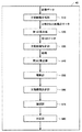
まず、図1を参照して、薄型パネルの製造工程について説明する。図1は、薄型パネルを製造する工程のうち、主たる工程を表わすフローチャートである。
<First Embodiment>
First, with reference to FIG. 1, the manufacturing process of a thin panel is demonstrated. FIG. 1 is a flowchart showing main steps among the steps of manufacturing a thin panel.
ステップS110にて、薄膜成膜工程として、基板に薄膜が形成される。ステップS120にて、レジスト膜形成工程において、レジスト膜形成装置が上記薄膜上にレジスト膜を形成する。ステップS130にて、露光装置が上記レジスト膜にパターンを転写する。ステップS140にて、現像工程として、パターン部以外のレジスト膜が除去される。 In step S110, a thin film is formed on the substrate as a thin film forming step. In step S120, in the resist film forming step, the resist film forming apparatus forms a resist film on the thin film. In step S130, the exposure apparatus transfers the pattern to the resist film. In step S140, as a developing process, the resist film other than the pattern portion is removed.
ステップS150にて、現像後の基板の状態が検査される。当該検査は、後述する画像処理技術によって行なわれる。 In step S150, the state of the substrate after development is inspected. The inspection is performed by an image processing technique described later.
ステップS160にて、現像後の基板から、不要な薄膜が除去される。ステップS170にて、レジスト除去工程として、基板に残存するレジストが除去される。 In step S160, an unnecessary thin film is removed from the developed substrate. In step S170, the resist remaining on the substrate is removed as a resist removal step.
次に、図2を参照して、本実施の形態に係る製造システム1について説明する。図2は、製造システム1の構成を表わす図である。製造システム1は、前工程10と、レジスト塗布装置12と、検査システム14と、次工程16と、制御装置18と、洗浄装置20と、搬送装置22,24,26とを備える。
Next, the manufacturing system 1 according to the present embodiment will be described with reference to FIG. FIG. 2 is a diagram illustrating the configuration of the manufacturing system 1. The manufacturing system 1 includes a pre-process 10, a resist
前工程10は、ステップS110における薄膜を形成するための装置を含む。前工程10において薄膜が形成されたガラス基板は、搬送装置22によってレジスト塗布装置12に搬入される。
The pre-process 10 includes an apparatus for forming a thin film in step S110. The glass substrate on which the thin film has been formed in the
レジスト塗布装置12は、薄膜が形成された基板上にレジストを塗布する。レジスト塗布装置12は、たとえばスキャニング方式を用いる装置であるが、スピン方式を用いる装置であってもよい。レジスト膜が形成されると、露光処理(ステップS130)と現像処理(ステップS140)とが行なわれ、その後、基板は搬送装置24によって検査システム14に搬入される。
The resist
検査システム14は、撮像装置と画像処理検査装置とを備える。検査システム14において、白色光がガラス基板に照射され、撮像装置が、その反射光を撮影し、基盤の画像データを取得する。画像処理検査装置は、その画像データを用いて画像処理を実行し、ガラス基板に存在し得る欠陥の有無を判断する。検査システム14によって得られた検査結果は、制御装置18に送られる。検査が完了した基板は、搬送装置26によって次工程16に搬入される。
The
次工程16は、たとえば、エッチング工程(ステップS160)とレジスト除去工程(ステップS170)とを含む。
The
制御装置18は、検査システム14から与えられる検査結果に基づいて、レジスト塗布装置12および洗浄装置20の作動条件を制御する。たとえば、検査システム14による検査の結果、基板に欠陥が存在していることが検出されると、制御装置18は、レジスト塗布装置12に対してレジスト塗布を中断するように命令を送る。また、検査の結果、レジスト塗布装置12におけるノズル(図示しない)の洗浄が必要であると判断すると、制御装置18は、洗浄装置20に対してレジスト塗布装置12を構成するノズルの洗浄を命令する。この場合、レジスト塗布装置12から洗浄装置20に対して、ノズルが移動する。
The
図3を参照して、レジスト塗布装置12について説明する。図3は、レジスト塗布装置12の一部を表わす図である。レジスト塗布装置12は、たとえばスキャニング方式により基板にレジストを塗布する。具体的には、レジスト塗布装置12は、基板30にレジストを供給するためのノズル32を備える。レジスト塗布装置12は、ノズル32を基板30に対して予め定められた一方向に移動し、レジスト34を基板30の表面に塗布する。
The resist
なお、レジスト塗布装置12の形式は、スキャニング方式による所謂スピンレスコータと称されるものに限られず、スピン方式による所謂スピンコータであってもよい。
The form of the resist
次に、図4を参照して、本実施の形態に係る検査装置40を備える検査システム14について説明する。図4は、検査システム14のシステム構成を表わす図である。検査システム14は、ライト46と、カメラ48と、検査装置40と、ディスプレイ装置50とを備える。検査装置40は、画像入力部41と、記憶部42と、演算部43と、出力部44と、入力部45とを含む。
Next, with reference to FIG. 4, the
検査対象物としての基板30は、レジスト塗布装置12から検査システム14に搬入され、ステージ(図示しない)において予め定められた位置に配置される。なお、検査対象物は、基板30に限られず、たとえば、液晶パネル、半導体、電子部品、プラスチック、金属、木材、紙、布その他のいずれであってもよい。液晶パネルの製造局面においては、基板30には、レジストが塗布されている。基板30は、カメラ48によって撮影され、撮影後、ステージの外部に搬出される。その後、別のガラス基板がステージに搬入され、前述の処理が繰り返される。
A
ライト46は、検査装置40からの発光命令に基づいて、当該位置に配置された基板30に対して、予め設定された強度を有する光を照射する。照射される光は、たとえば一般白色光である。
Based on the light emission command from the
カメラ48は、基板30からの反射光を受けて撮影し、画像データとして検査装置40に出力する。カメラ48は、検査装置40から出力された信号に応答して、基板30からの反射光を撮影する。カメラ48は、たとえばCCD(Charge Coupled Device)方式、CMOS(Complementary Mental Oxide Semiconductor)方式その他の方式により実現される。カメラ48は、基板30の撮影により取得したデータを画像データとして検査装置40に送出する。検査装置40は、画像入力部41を介してその画像データの入力を受け、記憶部42に格納する。なお、カメラ48は、エリアセンサカメラ、ラインセンサカメラのいずれでもよい。
The
記憶部42は、検査装置40の外部から与えられたデータと、検査装置40において生成されたデータとを格納する。外部から与えられたデータは、たとえば、上記画像データ、検査装置40の動作を規定する設定値等を含む。当該生成されたデータは、演算部43によって算出された画像処理のためのデータ、検査結果等を含む。
The
記憶部42は、データを不揮発的におよび揮発的に格納する。データを不揮発的に格納する記憶部42は、たとえば、大容量のデータを記憶可能なハードディスク等によって実現される。なお、記憶部42は、ハードディスクに限定されることなく、電源を供給されなくてもデータを保持可能な不揮発性の記憶装置(たとえば、フラッシュメモリ)であればよい。
The
具体的には、記憶部42は、データの消去・書き込みを何度でも行えるEPROM(Erasable Programmable Read Only Memory)、電気的に内容を書き換えることができるEEPROM(Electronically Erasable and Programmable ROM)、紫外線を使ってデータの消去・再書き込みを何度でも行えるUV(Ultra-Violet)−EPROM、その他、不揮発的にデータを記憶保持可能な構成を有する回路のいずれであってもよい。
Specifically, the
また、データを揮発的に格納する記憶部42は、演算部43によって使用されるデータを一時的に保持するワークメモリとして機能する。この場合、記憶部42は、たとえば、データを一時的に記憶可能なRAM(Random Access Memory)、SRAM(Static RAM)、DRAM(Dynamic RAM)、SDRAM(Synchronous DRAM)、ダブルデータレートモードという高速なデータ転送機能を持ったSDRAMであるDDR−SDRAM(Double Data Rate SDRAM)、Rambus社が開発した高速インターフェース技術を採用したDRAMであるRDRAM(Rambus Dynamic RAM)、Direct−RDRAM(Direct RDRAM)、その他、データを揮発的に記憶保持可能な構成を有する回路のいずれであってもよい。
The
演算部43は、記憶部42に格納されている画像データと、予め準備されているデータとを用いて、予め規定された画像処理を実行する。演算部43は、記憶部42に記憶されたプログラムに従って、画像を生成するための指示と、当該画像をディスプレイ装置50に表示させる指示(以下「描画指示」という)とを出力する。また、他の局面において、演算部43は、通信インターフェイスを介して、検査装置40の外部の装置(たとえば制御装置18)との通信を制御する。
The
演算部43は、具体的には、マイクロプロセッサ、プログラミングすることができるLSI(Large Scale Integration)であるFPGA(Field Programmable Gate Array)、特定の用途のために設計、製造される集積回路であるASIC(Application Specific Integrated Circuit)、その他の演算機能を有する回路により実現される。この場合、検査装置40の主たる機能は、ハードウェアとソフトウェアとの協働によって実現される。具体的には、当該機能は、演算部43が予め準備されたプログラムを実行することにより実現される。
Specifically, the
あるいは、他の局面においては、ハードウェアの組み合わせとして実現可能である。この場合、演算部43は、当該プログラムにより実現される処理を実行するために構成された回路、たとえばFPGA(Fiend Programmable Gate Array)などによって実現され得る。
Or in another situation, it is realizable as a combination of hardware. In this case, the
出力部44は、演算部43によって生成されたデータを、ディスプレイ装置50に出力する。ディスプレイ装置50は、そのデータに基づいて画像を表示する。ディスプレイ装置50は、たとえば、カメラ48によって撮影された原画像と、画像処理に基づいて検出されたレジストの塗布ムラが含まれる欠陥の画像とを表示する。また、ディスプレイ装置50は、基板30の検査の結果を表示してもよい。
The
入力部45は、外部からデータあるいは指示の入力を受け付ける。入力部45は、たとえばディスプレイ装置50の表面に装着されるタッチパネル、タッチパッド、キーボード、ペンタブレット、マウスその他のポインティングデバイスなどによって実現される。
The
ディスプレイ装置50は、検査装置40のユーザ(オペレータ)に各種の情報を、文字や画像等で表示する。ディスプレイ装置50は、検査装置40から出力された画像データに基づいた画像を表示する。具体的には、ディスプレイ装置50は、記憶部42の画像表示領域に格納されているデータを参照して、そのデータに応じた画像を表示する。ディスプレイ装置50は、たとえば、液晶ディスプレイ装置、CRT(Cathode Ray Tube)、FED(Field Emission Display)、PDP(Plasma Display Panel)、有機EL(Electro Luminescence)ディスプレイ、ドットマトリクス等その他の画像表示方式の表示機器のいずれであってもよい。
The
次に、図5を参照して、基板30に生じる線状の欠陥について説明する。図5(A)は、基板30を撮影することにより取得された画像を表わす図である。図5(B)は、当該画像の一部を分割した状態を表わす図である。
Next, with reference to FIG. 5, the linear defect which arises in the board |
カメラ48が基板30を撮影すると、画像52が取得される。基板30に対しては、検査の対象となる領域54が予め設定されている。この領域54は、たとえば入力部45に当該領域を規定するデータを与えることにより特定される。
When the
画像52を用いて演算部43が画像処理を実行すると、図5(B)に示されるように、短冊状に分割された画像が生成される。各画像の中には、周囲の輝度値よりも小さな輝度値を有するもの(すなわち周りよりも暗い領域を有するもの)と、周囲の輝度値よりも大きな輝度値を有する領域(周りの領域よりも明るい部分)とが含まれる。たとえば、領域56−1,56−2,56−3,56−4は、周りの領域よりも明るい領域(以下、「白筋」という)として検出される。一方、領域58−1,58−2は、周りの領域よりも輝度値が少ない領域(以下、「黒筋」という)として検出される。このような白筋あるいは黒筋が一方向に並んでいると、これらの領域は線状の欠陥として検出される。
When the
次に、図6を参照して、本実施の形態に係る欠陥の検出方法について説明する。図6は、図5に示されるような線状の欠陥を検出するために行なわれる手続の流れを表わす図である。 Next, the defect detection method according to the present embodiment will be described with reference to FIG. FIG. 6 is a diagram showing a flow of procedures performed to detect a linear defect as shown in FIG.
図6(A)に示されるように、基板30の撮影により取得された画像52は、複数の矩形状の画像に分割される(以下、「分割画像」という)。各分割画像において、周囲の輝度値と異なる輝度値を有する領域(筋候補A)が認識される。なお、当該領域が認識されない場合もある。また、領域が認識される場合には、その領域の数は検査対象に応じて異なる。
As shown in FIG. 6A, the
白筋の輝度値と黒筋の輝度値とは異なるため、輝度値の符号(正負)のいずれかが反転され、どちらか一方の符号に統一される。各領域の輝度値は、予め定められた方向610に沿って積算される。さらに、平均値が、その積算値に基づいて算出される。
Since the luminance value of the white stripe and the luminance value of the black stripe are different, one of the signs (positive or negative) of the luminance value is inverted and unified to one of the signs. The luminance value of each area is integrated along a
平均値が算出されると、図6(B)に示されるように、予め準備された閾値と平均値とに基づいて、各々の候補が欠陥であるか否かが判断される。図6(B)に示される例では、筋候補Bは、当該閾値(弱筋ムラ位置判定閾値620)を上回るため、欠陥の候補として特定される(スジ候補B)。その他のものは、当該閾値を下回るためノイズとして扱われる。 When the average value is calculated, as shown in FIG. 6B, it is determined whether or not each candidate is defective based on a threshold value and an average value prepared in advance. In the example shown in FIG. 6B, the muscle candidate B exceeds the threshold value (weak muscle unevenness position determination threshold value 620), and thus is specified as a defect candidate (streak candidate B). Others are treated as noise because they are below the threshold.
次に、図6(C)に示されるように、検出された弱筋ムラ候補の各々について、コントラストと位置とに基づいて、その位置候補に筋ムラ候補が存在するか否かが確認される。具体的には、スジ候補Aについてそのコントラストが予め設定されたコントラスト閾値を上回るか否か、および当該位置が中心位置に対して予め設定された範囲内のずれであるか否かが確認される。なお、スジ候補Cは、前記2つの条件を満足するスジ候補Aに対応するものである。 Next, as shown in FIG. 6C, for each detected weak muscle unevenness candidate, whether or not a muscle unevenness candidate exists in the position candidate is confirmed based on the contrast and the position. . Specifically, it is confirmed whether or not the contrast of the streak candidate A exceeds a preset contrast threshold, and whether or not the position is within a preset range with respect to the center position. . The streak candidate C corresponds to the streak candidate A that satisfies the two conditions.
最後に、図6(D)に示されるように、各分割画像について、上記の条件を満足する筋ムラ候補がどの程度の割合で存在するかが確認される。具体的には、その条件を満足する筋ムラ候補と全分割画像の数との比率が求められる。その比率が予め設定された(弱筋ムラ位置の候補存在率)を上回る場合には、当該弱筋ムラが存在すると判断される。 Finally, as shown in FIG. 6 (D), it is confirmed for each divided image how often the stripe unevenness candidate satisfying the above condition exists. Specifically, a ratio between the stripe unevenness candidate that satisfies the condition and the number of all divided images is obtained. When the ratio exceeds a preset (candidate ratio of weak muscle unevenness position), it is determined that the weak muscle unevenness exists.
次に、図7を参照して、検査装置40のデータ構造について説明する。図7は、記憶部42におけるデータの格納の一態様を概念的に表わす図である。記憶部42は、データを格納するための複数の領域を含む。
Next, the data structure of the
分割画像の画素数(DPIX)は、領域710に格納されている。当該分割画像の画素数は、取得された画像データを分割するための画素数を規定する。たとえば、縦方向の画素数が500画素である画像データが使用される場合、画素数DPIXの値が100であるため、画像データは5分割される。分割画像内に含まれる線状の欠陥候補の輝度値の差分(BDA)は、領域720に格納されている。複数の分割画像に跨る線状の欠陥を抽出するための閾値(THA)は、領域730に格納されている。複数の分割画像に跨る線状の欠陥を抽出するための第2の閾値(THB)は、領域740に格納されている。
The number of pixels (DPIX) of the divided image is stored in
カメラ48によって取得された画像データは、領域750に格納されている。或る局面においては、画像データは、各々が異なる複数種類の画像のデータから構成されるデータベースを構成する。
Image data acquired by the
領域710から領域740に格納されているデータは、たとえば入力部45を介して入力される。また他の局面においては、これらのデータは、制御装置18から送信されるものでもよい。
The data stored in the
次に、図8を参照して、本実施の形態に係る検査装置40を実現する演算部43について説明する。図8は、演算部43によって実現される機能の構成を表わすブロック図である。各機能は、演算部43として機能するCPUその他のプロセッサが各機能を実現するためのプログラムを実行することにより実現される。具体的には、演算部43は、分割画像生成部810と、第1の算出部820と、欠陥候補特定部830と、第2の算出部840と、積算部850と、欠陥範囲決定部860とを含む。
Next, with reference to FIG. 8, the calculating
演算部43は、記憶部42から、基板30の撮像により取得された画像データを読み出す。分割画像生成部810は、その画像データを第1の方向に沿って分割し、複数の分割画像を生成する。具体的には、分割画像生成部810は、画素数DPIX(領域710)の値に従って、画像を複数の画像に分割する。
The
第1の算出部820は、その分割画像データに基づいて、各々を構成する複数の領域の輝度値であって当該第1の方向に直交する第2の方向に沿う領域の輝度値に基づいて第1のデータを算出する。具体的には、第1の算出部820は、線状の欠陥が発生する方向と平行な方向に当該分割画像の輝度値の平均値を算出する。
Based on the divided image data, the
欠陥候補特定部830は、第1の算出部820によって算出された当該第1のデータに基づいて、各分割画像における線状の欠陥候補が含まれる範囲をそれぞれ特定する。具体的には、欠陥候補特定部830は、記憶部42に格納されている輝度値の差分(BDA)を用いて、上記範囲をそれぞれ特定する。
Based on the first data calculated by the
第2の算出部840は、欠陥候補特定部830によって特定された範囲に対応する画像データを用いて、各範囲が強調されたデータ(第2のデータ)をそれぞれ算出する。具体的には、ある局面において、第2の算出部840は、各範囲に対応する画像データの符号を正または負のいずれかに揃えることにより、当該第2のデータを算出する。
The
他の局面においては、第2の算出部840は、当該範囲以外の範囲よりもその範囲が明るい場合、または、当該範囲の範囲以外の範囲よりもその欠陥候補が暗い場合には、各画像データの符号を反転させて、符号が反転された後の画像データを加算することにより、上記第2のデータを算出する。
In another aspect, the
さらに他の局面において、第2の算出部84は、上記線状の欠陥候補の強度を算出する。その強度が予め設定された基準値を下回る場合には、第2の算出部840は、その基準値を下回る強度を有する上記欠陥候補範囲の画像データを、当該第2のデータの算出の対象から除外する。
In still another aspect, the second calculation unit 84 calculates the strength of the linear defect candidate. When the intensity falls below a preset reference value, the
積算部850は、第2の算出部840によって算出された第2のデータを、上記第2の方向(たとえば線状の欠陥が発生する方向)に沿って積算する。
The
欠陥範囲決定部860は、積算部850によって算出されたデータに基づいて、当該線状の欠陥の範囲を決定する。具体的には、欠陥範囲決定部860は、線状欠陥抽出閾値(THA)を用いて、算出されたデータに対応する領域が線状の欠陥であるか否かを判断する。
The defect
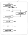
次に、図9から図18を参照して、本実施の形態に係る検査装置40の動作について説明する。図9は、演算部43が実行する一連の処理の一部を表わすフローチャートである。図10は、基板30を撮影することにより得られた画像データ1000における欠陥の状態を表わす図である。図11は、図10に示される線状の欠陥の濃淡プロファイルを表わす図である。図12は、画像データ1000における画像分割方法および画像を分割する方向を表わす図である。図13は、各分割画像の1次元の投影データを表わす図である。図14は、1次元データから線状の欠陥候補を抽出するプロセスを表わす図である。図15は、各1次元の投影データについて輝度値の平均値とX座標値との関係を表わす図である。図16は、欠陥候補を強調して得られたデータについて、輝度値の差とX座標値との関係を表わす図である。図17は、各1次元の投影データについて輝度値の差とX座標値との関係を表わす図である。図18は、輝度値の差の平均値とX座標値との関係を表わす図である。
Next, the operation of the
ここでは、図10に示されるように、画像データ1000をもたらす基板1010から、線状の欠陥1020を検出する場合について説明する。ここで、画像データ1000のX座標は、たとえば方向1030に沿って規定され、Y座標は、方向1040に沿って規定される。画像データ1000において線状の欠陥1020の領域以外の撮像画像中の輝度値Bgoodは「128」であり、線状の欠陥1020のA−B上の濃淡プロファイルは、図11に示すような変化がある。
Here, as shown in FIG. 10, a case where a
なお、図10に示される画像データ1000以外の一般的な撮像画像における線状の欠陥領域以外の撮像画像中の輝度値Bgoodとして、画像全体の平均輝度値を適用することが考えられる。また、原画像データの中に良品画像が存在するのであれば、当該良品画像を用いて平均輝度値を算出して適用してもよい。
Note that it is conceivable to apply the average luminance value of the entire image as the luminance value Bgood in the captured image other than the linear defect area in the general captured image other than the
また、撮像画像の欠陥領域以外および良品画像に関し、濃淡変化が大きい場合には、モフォロジ処理を用いることにより、線状欠陥をさらに高精度に検出できる。モフォロジ処理を用いる態様は、後述する(第3の実施の形態)。 Further, when the density change is large with respect to the non-defective region of the captured image and the non-defective image, the linear defect can be detected with higher accuracy by using the morphology process. A mode using the morphology processing will be described later (third embodiment).
まず、図9を参照して、ステップS910にて、検査装置40は、初期設定を受け付ける。具体的には、検査装置40のオペレータが、入力部45を介して、分割画像画素数(DPIX)と、輝度の差分(BDA)と、閾値(THA、THB)とを入力すると、演算部43は、これらのデータを記憶部42に格納する(領域710〜740)。
First, referring to FIG. 9, in step S910,
ステップS920にて、演算部43は、カメラ48から出力された原画像データの入力を受けて、画像データ1000として、そのデータを記憶部42に格納する(領域750)。
In step S920, the
ステップS930にて、演算部43は、領域750から画像データ1000をワーク領域に読み出す。ワーク領域は、演算部43が処理を実行する際に、記憶部42に確保される。演算部43は、画素数(DPIX)を用いて、線状の欠陥が発生する方向に対して垂直な方向に当該画像データを分割することにより、分割画像データを生成する。
In step S930,
たとえば、図12に示されるように、画像データ1000は、画像を分割する方向1050に対して平行に分割され、分割画像IDA(1210)〜分割画像IDE(1250)が生成される。演算部43は、縦500画素である画像データ1000を分割画像の画素数DPIX(=100)毎に分割するため、本実施の形態においては画像データ1000を5分割することとなる。
For example, as shown in FIG. 12, the
線状の欠陥の発生する方向(本実施の形態においては図12の方向1040)の画素数を分割画像の画素数DPIXで割った時に余りが生じる場合には、最後の分割画像は、画像の分割を開始した一方の画像端と異なる他方の画像端から分割画像の画素数DPIX分を用いるものとする。この場合、最後に生成された分割画像とその直前に生成された分割画像との間には、一部で重複する領域が存在することとなる。
If a remainder occurs when the number of pixels in the direction in which the linear defect occurs (
ステップS940にて、演算部43は、分割画像毎に濃淡を投影(1次元化)する。具体的には、演算部43は、各分割画像について、当該画像データを線状の欠陥が発生する方向と平行な方向に積算する。具体的には、図10に示されるように、演算部43は、積算する方向1040として規定されたY座標軸の正方向に沿って、同一のX座標値を有する各画素の輝度値を積算する。さらに、演算部43は、当該積算値についてY座標軸方向の画素数を用いて除算処理を実行することにより輝度値の平均値を求める(第1のデータ)。ステップS940において算出されたデータは、たとえば図13においては、各分割画像の1次元投影データIDPA,IDPB,IDPC,IDPD,IDPE(1310,1320,1330,1340,1350)として表わされる。
In step S940, the
ステップS950にて、演算部43は、分割画像ごとに、上記の1次元投影データを用いて当該分割画像内における線状の欠陥の候補である線状欠陥候補Aを抽出する。この処理を、図13および図14を参照して、図13に示される1次元投影データIDPA(1310)を用いて具体的に説明する。まず、図14に示されるように、画像データ1000における線状の欠陥1020の領域以外の撮影画像中の輝度値(Bgood)と、上記分割画像内の線状の欠陥候補輝度値の差分(BDA)を用いて、1次元の投影データの値が138(=Bgood+BDA=128+10)以上のX座標の範囲、または、1次元投影データが118(=Bgood−BDA=128−10)以下のX座標の範囲を決定する。図14に示されるように、分割画像の1次元投影データIPDA(1310)については、X_LとX_Rとの間が、線状欠陥候補A(SA_IDPA1)となる。演算部43は、すべての1次元投影データIPDA(1310)〜IPDE(1350)について同様の処理を実行する。その結果は、図15に示される。
In step S950, the
ステップS960にて、演算部43は、欠陥候補が強調された1次元のデータ(欠陥候補強調1次元データ)を生成する。具体的には、演算部43は、ステップS950において抽出した線状欠陥候補Aの範囲の1次元投影データIPDA(1310)を用いて、輝度値Bgoodとの差を算出し、その値の絶対値を求める。演算部43は、さらに、その他の範囲の値を0とし、欠陥候補強調1次元データを生成する。たとえば、図15に示される1次元投影データIPDA(1310)が使用されると、そのデータに基づく欠陥候補強調1次元データは、図16に示されるように求められる。演算部43は、図15に示される全てのデータについて当該データを算出する。その結果は、図17に示される。
In step S960,
ステップS970にて、演算部43は、すべての分割画像の各々について、ステップS960において生成された欠陥候補強調1次元データを積算する。具体的には、演算部43は、図17に示される積算方向1710に沿って、同一のX座標値を有する各欠陥候補強調1次元データを積算する。さらに、演算部43は、当該積算によって得られた値を分割画像数で除することにより、欠陥候補が強調された1次元データの平均値を算出する。一例として、図17に示されるデータを用いて得られた平均値は、図18に示される。
In step S970,
ステップS980にて、演算部43は、ステップS970において生成した平均値を用いて、複数の分割画像に跨る線状の欠陥を抽出する。具体的には、演算部43は、上記平均値の中から、線状の欠陥を抽出するための閾値(THB)の値を上回るX座標の範囲を特定する。たとえば、図18に示される例では、X座標値(X_L)とX座標値(X_R)との間が閾値THBを上回るため、演算部43は、当該複数の分割画像に跨る線状の欠陥がこの範囲に存在すると判断する。演算部43は、その判断の結果と当該画像データ1000とを関連付けて、検査結果として、記憶部42において確保した領域に格納する。
In step S980, the
以上により、画像データ1000を用いて、基板1010に含まれる線状の欠陥1020が検出される。
As described above, the
ここで、上記の処理に追加可能な処理について説明する。まず、ステップS910の初期設定において、演算部43は、分割画像から線状の欠陥候補を抽出するための閾値THAを設定する。本実施の形態においては、閾値THA=10とする。
Here, processing that can be added to the above processing will be described. First, in the initial setting in step S910, the
次に、ステップS960において、演算部43は、線状欠陥候補Aの強度を算出する。この強度を算出する一例として、演算部43は、各線状欠陥候補Aについて、欠陥候補強調1次元データ(第1のデータ)の値が最大のものを当該強度とする。たとえば、図16におけるSA_IDPA1を参照すると、演算部43は、X_LとX_Rとの間の欠陥候補強調1次元データ値の中の最大値を強度として算出する。さらに、演算部43は、線状欠陥候補Aの強度が閾値THA以上である線状欠陥候補Aを「真の」線状欠陥候補Aとして分類し、それ以外の線状欠陥候補Aを排除するために、閾値THA未満の強度を有する線状欠陥候補Aの範囲の欠陥候補強調1次元データの値をすべて「0」にする。
Next, in step S960, the
ステップS960において追加される上記の処理により、真の線状欠陥以外の成分であると考えられるノイズ成分を線状欠陥候補Aの段階で排除することが可能であるため、本実施の形態に係る検査装置40は、線状の欠陥をより高精度に検出することができる。
According to the present embodiment, the noise component that is considered to be a component other than the true linear defect can be eliminated at the stage of the linear defect candidate A by the above processing added in step S960. The
なお、本実施の形態に係る線状欠陥候補Aの強度を算出する方法は、上記のような欠陥候補強調1次元データの中の最大値を使用する態様に限られない。 Note that the method of calculating the intensity of the linear defect candidate A according to the present embodiment is not limited to the aspect of using the maximum value in the defect candidate emphasizing one-dimensional data as described above.
その他の局面において、X_LとX_Rとの間の範囲における欠陥候補強調1次元データ値の平均値を算出し、その平均値を線状欠陥候補Aの強度としてもよい。線状欠陥の方向に対して垂直な方向に輝度値のランダムノイズがある場合にも、検査装置40は、より正確に線状欠陥候補Aを抽出可能である。
In another aspect, an average value of defect candidate emphasis one-dimensional data values in a range between X_L and X_R may be calculated, and the average value may be used as the intensity of the linear defect candidate A. Even when there is random noise of the luminance value in a direction perpendicular to the direction of the linear defect, the
さらにその他の局面において、別の算出方法が適用可能である。たとえば、X_LとX_Rとの範囲の長さをWX(=X_R−X_L)とする。演算部43は、X_LとX_Rの間の中央部WX/2の幅の欠陥候補強調1次元データ値の平均値を算出して、その平均値を線状欠陥候補Aの強度とする。これにより、演算部43が上記のようなX_LとX_Rとの間の全区間の欠陥候補強調1次元データ値の平均値を算出する場合に問題となる当該範囲の両端部の影響による線状欠陥候補Aの強度の低下が排除され得る。その結果、検査装置40は、より正確に線状欠陥候補Aを抽出できる。
Further, in other aspects, another calculation method can be applied. For example, let the length of the range between X_L and X_R be WX (= X_R−X_L). The
本実施の形態に係る検査装置40によると、ステップS960に記載のように、線状欠陥候補Aの範囲の1次元投影データと輝度値Bgoodとの差の絶対値として、欠陥候補強調1次元データを生成する。そのため、周囲より明るい線状欠陥と周囲より暗い線状欠陥とを区別無く扱うことができる。正のデータと負のデータとが単純に積算されることによる値の相殺が防止される。これにより、検査装置40は、濃淡変化がある線状の欠陥であっても高精度に抽出することができる。
According to the
また、ステップS970に記載のように、演算部43は、欠陥候補強調1次元データを、全分割画像分について積算し、積算によって得られたデータの平均値を算出する。そのため、検査装置40は、複数の線分に分裂した線状の欠陥を高精度に抽出することができる。
Further, as described in step S970, the
さらに、ステップS960およびステップS970に記載のように、演算部43は、線状欠陥候補Aの範囲以外の欠陥候補強調1次元データを0にすることで、ノイズ成分を有するデータが使用される処理の前の段階で削除している。そのため、上記の欠陥候補協調1次元データを積算して積算値から平均値を算出した後において、ノイズ成分のみの積算によるノイズ成分の強度が上昇することによる誤検出の発生が防止され得る。結果として、検査装置40は、誤検出することなく高精度に線状の欠陥を抽出できる。
Further, as described in Step S960 and Step S970, the
<変形例>
以下、本実施の形態の変形例について説明する。本変形例に係る製造方法は、検査装置40による検査の結果に応じてガラス基板の製造工程を変更する指示を出力できる点で、前述の製造方法と異なる。
<Modification>
Hereinafter, modifications of the present embodiment will be described. The manufacturing method according to this modified example is different from the above-described manufacturing method in that it can output an instruction to change the manufacturing process of the glass substrate according to the result of the inspection by the
そこで、図19を参照して、本変形例に係る製造方法について説明する。図19は、本変形例に係る製造方法を表わすフローチャートである。なお、前述の処理と同一の処理には同一のステップ番号を付してある。したがって、ここではそれらについての説明は繰り返さない。 Accordingly, a manufacturing method according to this modification will be described with reference to FIG. FIG. 19 is a flowchart showing a manufacturing method according to this modification. The same steps as those described above are denoted by the same step numbers. Therefore, description thereof will not be repeated here.
ステップS1910にて、検査装置40による検査の結果が良好であるか否かが判断される。具体的には、制御装置18は、検査システム14から送られる検査結果が予め設定された基準値を満足するか否かを判断する。検査結果が当該基準値を上回る場合には、制御装置18は、そのガラス基板の加工は規定どおり行なわれたと判断し(ステップS1910にてYES)、当該ガラス基板を次工程16に搬入する指示を出力する。搬入後、具体的には、ステップS160にて、当該基板に対するエッチングが行なわれる。
In step S1910, it is determined whether the result of the inspection by
一方、検査結果が良好でない場合には(ステップS1910にてNO)、制御装置18は、その加工は規定どおり行なわれなかったと判断し、当該ガラス基板を再加工する命令を出力する。この命令に応答して、当該ガラス基板はリワーク工程に搬送される。具体的には、ステップS1920にて、ガラス基板は塗布されたレジスト膜が一旦除去され、洗浄された後再びレジスト膜形成工程に搬入される。
On the other hand, if the inspection result is not good (NO in step S1910),
以上のようにして、本変形例に係る製造方法によると、検査システム14から出力される検査結果が規定以下である場合には、ガラス基板の再加工が行なわれる。その結果、仕様を満足しないガラス基板を用いた半導体基板の製造が行なわれることが防止される。
As described above, according to the manufacturing method according to the present modification, when the inspection result output from the
<第2の実施の形態>
以下、本発明の第2の実施の形態について説明する。
<Second Embodiment>
Hereinafter, a second embodiment of the present invention will be described.
図20は、本実施の形態に係る検査装置が備える演算部43によって実現される機能の構成を表わすブロック図である。演算部43は、図8に示される構成に加えて、確認部870と判定部880とをさらに備える。
FIG. 20 is a block diagram showing a configuration of functions realized by
欠陥候補特定部830は、分割により生成された分割画像データに基づいて、分割画像における線状の欠陥候補が含まれる範囲(第1の欠陥候補範囲)をそれぞれ特定する。
The defect
第2の算出部840は、第1の欠陥候補範囲に対応する画像データに基づいて線状の欠陥候補の強度をそれぞれ算出する。さらに、第2の算出部840は、第2のデータとして、当該強度に基づいて、当該第1の欠陥候補範囲が強調されたデータ(欠陥候補強調1次元データ)を算出する。
The
積算部850は、上述の第2の方向(線状の欠陥が発生する方向)に沿って当該第2のデータを積算する。
The accumulating
欠陥範囲決定部860は、第2のデータを積算することによって得られたデータに基づいて、複数の分割画像のうちの少なくとも2つの分割画像に跨る線状の欠陥候補が含まれる第2の欠陥候補範囲を決定する。具体的には、欠陥範囲決定部860は、各分割画像について、予め規定された閾値との差が予め定められた値を上回る輝度値を有する上記第1の欠陥候補範囲をそれぞれ特定する。欠陥範囲決定部860は、その特定された第1の欠陥候補範囲について、上記第1の方向に沿う座標軸上の範囲をそれぞれ特定する。欠陥範囲決定部860は、各第1の欠陥候補範囲について、その特定された座標軸上の範囲の各々が重複しているか否かを判断する。欠陥範囲決定部860は、その特定された座標軸上の範囲の各々が重複している第1の欠陥候補範囲を、第2の欠陥候補範囲として決定する。
The defect
確認部870は、当該第2の欠陥候補範囲の中に、予め既定された条件を満足する線状の欠陥が存在するか否かを確認する。具体的には、確認部870は、上記第1の欠陥候補範囲について、第1の方向に従う座標軸上の範囲の第1の中央値を算出する。確認部870は、第2の欠陥候補範囲について、第1の方向に沿う座標軸上の範囲の第2の中央値を算出する。確認部870は、その第1の中央値と第2の中央値との差を算出し、その差が予め設定された許容誤差の範囲内であるか否かを確認する。確認部870は、その差が当該許容誤差の範囲内である場合に、線状の欠陥が第2の欠陥候補範囲に存在すると判断する。
The
判定部880は、上記条件を満足する線状の欠陥が含まれる分割画像が複数の分割画像の中に存在する割合に基づいて、線状の欠陥の有無を判定する。
The
次に、図21を参照して、本実施の形態に係る検査装置のデータ構造について説明する。図21は、記憶部42におけるデータの格納の一態様を概念的に表わす図である。
Next, a data structure of the inspection apparatus according to the present embodiment will be described with reference to FIG. FIG. 21 is a diagram conceptually showing one mode of data storage in
複数の分割画像に跨る線状の欠陥を抽出するための閾値(THB2)は、領域2040に格納されている。分割画像内の線状の欠陥候補を再確認するための閾値(THC)は、領域2050に格納されている。線状の欠陥の位置ズレの許容誤差を規定する画素数(SCDPIX)は、領域2060に格納されている。線状の欠陥が分割画像に存在するか否かを判断するための割合(SCR)は、領域2070に格納されている。これらのデータも、入力部45を介して入力される。
A threshold (THB2) for extracting a linear defect across a plurality of divided images is stored in the
図22を参照して、本発明の第2の実施の形態に係る検査装置の制御構造について説明する。図22は、本発明の第2の実施の形態に係る検査装置が実行する一連の動作を表わすフローチャートである。ここでは、図4に示される構成を用いて説明する。また、第1の実施の形態における動作と同一の動作には同一のステップ番号を付してある。したがって、ここではそれらについての説明は繰り返さない。 With reference to FIG. 22, the control structure of the inspection apparatus according to the second embodiment of the present invention will be described. FIG. 22 is a flowchart showing a series of operations executed by the inspection apparatus according to the second embodiment of the present invention. Here, description will be made using the configuration shown in FIG. Also, the same step numbers are assigned to the same operations as those in the first embodiment. Therefore, description thereof will not be repeated here.
ステップS2110にて、検査装置40の演算部43は、初期設定のためのデータの入力を受け付ける。具体的には、演算部43は、分割画像の画素数(DPIX)と、輝度値の差分(BDA)と、閾値(THA、THB2、THC)と、位置ズレ誤差許容画素数(SCDPIX)と、線状の欠陥候補存在率(SCR)との入力をそれぞれ受け付け、記憶部42において予め確保した領域にそれらのデータを書き込む。さらに、演算部43は、既にカメラ48から検査装置40に入力されていた原画像データ1000をワーク領域に読み込み、第1の実施の形態において示された処理と同様の処理を実行する(ステップS920〜S950)。
In step S2110,
ステップS2120にて、演算部43は、ステップS950において決定された線状欠陥候補Aの範囲の1次元のデータと輝度値Bgoodとの差を算出する。演算部43は、その差の絶対値を求め、その他の範囲の値を0とすることにより、欠陥候補強調データ(第2のデータ)を算出する。その結果、図16に示されるように、欠陥候補強調1次元データが求められる。各分割画像について同様の処理が実行されると、前述の図17に示されるように、それぞれの値が得られる。
In step S2120,
演算部43は、線状欠陥候補Aの強度を算出する。一例として、演算部43は、各線状欠陥候補Aの欠陥候補強調1次元データの値が最大となるものを当該線状欠陥候補Aの強度とする。たとえば、欠陥候補範囲SA_IDPA1に関し、図16に示されるX_LとX_Rとの間の欠陥候補強調1次元データの値の最大値が強度として求められる。さらに、演算部43は、線状欠陥候補Aの強度が閾値(THA)以上である線状欠陥候補Aを「真の」線状欠陥候補Aとし、それ以外の線状欠陥候補Aを排除するために、分割画像内において閾値THA未満の強度を有する線状欠陥候補Aの範囲を特定する欠陥候補強調1次元データの値をすべて「0」に変更する。
The
ステップS970にて、演算部43は、欠陥候補1次元データを積算し、さらに、積算後のデータの平均値を算出する。
In step S970,
ステップS2130にて、演算部43は、ステップS970にて算出した平均値を用いて、複数の分割画像に跨る「線状欠陥候補B」を抽出する。具体的には、演算部43は、上記積算によって得られたデータの中で、X座標軸上において閾値(THB2)以上の範囲を特定する。たとえば、図18に示される例では、X_LとX_Rとの間が閾値(THB2)を上回るため(THB2=5)、演算部43は、複数の分割画像に跨るような線状欠陥候補Bが上記の範囲に存在すると判定する。
In step S <b> 2130, using the average value calculated in step S <b> 970,
ステップS2140にて、演算部43は、各分割画像ごとの1次元データについて、ステップS2130において特定した線状欠陥候補Bの範囲に、予め定められた条件を満足するような線状欠陥候補Aが存在するか否か確認する。ここで、当該条件は、たとえば、ステップS2130において特定された線状欠陥候補Bの範囲と線状欠陥候補Aの範囲との重なり度合、および、当該重なり度合の条件を満足する線状欠陥候補Aの強度である。
In step S2140, the
より詳しくは、重なり度合に関しては、演算部43は、線状欠陥候補Bの中央座標値BCXを算出する。図18に示される線状欠陥候補B(SB)の場合、X_LとX_Rの中央値が当該中央座標値BCXとして算出される。
More specifically, regarding the degree of overlap, the
次に、演算部43は、各線状欠陥候補Aについて、中央座標値ACXを同様に算出する。図14に示される線状欠陥候補A(SA_IDPA1)の場合、X_LとX_Rとの中央値が中央座標値ACXとして算出される。演算部43は、中央座標値BCXと中央座標値ACXとの差を算出する。ここで、上記重なり度合の条件とは、線状欠陥の位置ズレ誤差許容画素数SCDPIXを下回ることをいう。一方、線状欠陥候補Aの強度に関しては、ステップS2110において設定された閾値(THC)を上回ることが必要となる。演算部43は、これらの条件を満足する重なり度合および強度を有する線状欠陥候補Aを線状欠陥候補Cとして特定する。
Next, the
ステップS2150にて、演算部43は、個々の線状欠陥候補Bについて、どの程度の割合の分割画像に線状欠陥候補Cが存在するかを算出し、その割合が存在率SCR以上であるような線状欠陥候補Dを「真の線状欠陥」であると判定する。
In step S2150, for each linear defect candidate B, the
以上のようにして、本実施の形態に係る検査装置40によると、ステップS2140に記載のように、線状欠陥候補Bの範囲に本当に線状欠陥候補Aが存在するかを再び確認することで、線状欠陥候補Bが真の欠陥であるのか、あるいはノイズであるのかを、より正確に判定することができる。これにより、検査装置40は、濃淡変化がある線状の欠陥であっても高精度に検出することができる。
As described above, according to the
また、ステップS2150に記載のように、線状欠陥候補Cが存在する分割画像の割合を算出することにより、その割合と予め設定された基準値とを比較することにより、検査装置40は、線状欠陥候補Bが真の欠陥であるのか、あるいは、ノイズであるのかを、より正確に判定することができる。これにより、検査装置40は、濃淡変化がある線状の欠陥であっても高精度に抽出することができる。
Further, as described in step S2150, by calculating the ratio of the divided image in which the linear defect candidate C exists, the
<第3の実施の形態>
以下、本発明の第3の実施の形態について説明する。本実施の形態に係る検査装置40は、線状の欠陥候補の範囲を決定する際にモフォロジ処理を行なったデータを用いて当該範囲を決定する機能を有する点で、前述の各実施の形態と異なる。なお、本実施の形態に係る検査装置は、当該装置に固有な上記機能を有する処理をプロセッサにより実行させることにより実現される。その他の機能は、図4に示される検査装置40と同じである。そこで、図4に示される検査装置40の構成に基づいて、本実施の形態に係る検査装置を説明する。
<Third Embodiment>
Hereinafter, a third embodiment of the present invention will be described. The
図23を参照して、本実施の形態に係る検査装置の構成について説明する。図23は、検査装置40が備える演算部43によって実現される機能の構成を表わすブロック図である。演算部43は、図8に示される構成に加えて、モフォロジ処理部2210をさらに備える。モフォロジ処理部2210は、第1の算出部820からの出力に基づいて作動するように第1の算出部820に機能的に接続される。モフォロジ処理部2210からの出力は、欠陥候補特定部830に入力される。
With reference to FIG. 23, the configuration of the inspection apparatus according to the present embodiment will be described. FIG. 23 is a block diagram illustrating a configuration of functions realized by the
次に、図24を参照して、本実施の形態に係る検査装置40のデータ構造について説明する。図24は、検査装置40の記憶部42におけるデータの格納の一態様を概念的に表わす図である。
Next, the data structure of the
記憶部42において、モフォロジ処理フィルタサイズ(MFS)は、領域2310に格納されている。分割画像内の線状欠陥候補を抽出するための強度(BDTHA)は、領域2320に格納されている。これらのデータは、検査装置40のオペレータによって入力される。
In the
次に、図25〜図28を参照して、本実施の形態に係る検査装置40の制御構造について説明する。図25および図26は、本実施の形態に係る検査装置40を実現する演算部43が実行する一連の動作を表わすフローチャートである。なお、前述の動作と同一の動作には同一のステップ番号を付してある。したがって、ここではそれらについての説明は繰り返さない。図27は、モフォロジ処理による1次元データの変化を表わす図である。図28は、欠陥候補強調1次元データを表わす図である。
Next, a control structure of the
ステップS2410にて、演算部43は、検査装置40において予め規定された処理を実行するための初期値の入力を受け付ける。具体的には、演算部43は、分割画像の画素数(DPIX)と、モフォロジ処理フィルタサイズ(MFS)と、線状の欠陥候補を抽出するための強度(BDTHA)との入力を受けて、これらのデータを記憶部42に格納する(領域2310,2320)。本実施の形態においては、分割画像の画素数(DPIX)=100、モフォロジ処理フィルタサイズ(MFS)=11、強度(BDTHA)=1である。なお、データは上記のものに限られず、他の局面において、その他の値が用いられてもよい。
In step S2410,
ステップS920〜S940にて、演算部43は、前述のような処理を実行する。
ステップS2500にて、演算部43は、後述するモフォロジ処理を実行する(図26)。ステップS2420にて、演算部43は、モフォロジ処理において決定された線状欠陥候補Aに基づいて、欠陥候補が強調された1次元のデータ(欠陥候補強調1次元データ)を生成する。
In steps S920 to S940, the
In step S2500,
その後、演算部43は、欠陥候補強調1次元データの平均値を算出し(ステップS970)、その平均値に基づいて線状欠陥の領域を表わすデータを算出し、当該領域を特定する(ステップS980)。
Thereafter, the
図26を参照して、ステップS2510にて、演算部43は、周囲より明るい線状の欠陥が候補A(1)を抽出する。
Referring to FIG. 26, in step S2510,
ここで、図27を参照して、ステップS2510の処理について詳細に説明する。最初に、演算部43は、図27(A)に示されるようなデータに対して最小値フィルタ処理を実行する(周囲より明るい線状欠陥候補A(1)の抽出)。ここで、最小値フィルタのフィルタサイズはモフォロジ処理フィルタサイズ(MFS)であるため、演算部43は、注目画素の左右の5画素ずつを考慮した全11画素のうち最も小さい値を求め、当該注目画素の値をその最も小さい値に置き換える。
Here, with reference to FIG. 27, the process of step S2510 will be described in detail. First, the
図27(B)は、図27(A)に示される1次元のデータに対して上記の最小値フィルタ処理を行なって得られた結果を表わす図である。演算部43は、図27(B)に示される1次元データに対して最大値フィルタ処理を実行する。具体的には、最大値フィルタ処理におけるフィルタサイズがモフォロジ処理フィルタサイズ(MFS)であり、この値は本実施の形態においては「11」である。そこで、演算部43は、注目画素の左右の5画素隣までを考慮して、全11画素の中で最も大きい値を算出し、当該注目画素の値をその最も大きい値に変更する。
FIG. 27B is a diagram showing a result obtained by performing the minimum value filtering process on the one-dimensional data shown in FIG. The
図27(C)は、図27(B)に示される1次元データに対して最大値フィルタ処理を行なって得られた結果を表わす図である。 FIG. 27C is a diagram showing a result obtained by performing the maximum value filtering process on the one-dimensional data shown in FIG.
演算部43は、図27(A)に示される1次元データと図27(C)に示される1次元データとを用いて、各画素の位置の値の差分を算出し、その算出によって現われるピークの範囲が線状欠陥候補A(1)として特定する。演算部43は、当該ピークの範囲の最大値を線状欠陥候補A(1)の強度として特定し、記憶部42に格納する。図27(D)は、そのようにして得られた結果の1次元データを表わす図である。
The
図26を再び参照して、ステップS2520にて、演算部43は、周囲より暗い線状欠陥候補A(2)を抽出する。具体的には、演算部43は、1次元のデータに対して最大値フィルタ処理を行ない、処理後のデータを取得する。次に、演算部43は、その取得したデータに対して最小値フィルタ処理を実行し、処理後の1次元データを取得する。演算部43は、最初のフィルタ処理が実行される前の1次元データと、最小値フィルタ処理が行なわれた後の1次元データとの差分を算出し、記憶部42に格納する。ここで、当該差分によって得られたデータは、その性質上0以下の値となるため、当該データの絶対値を取得することにより、0以上の値のみを有する1次元データに変換する。この場合、ステップS2510における処理によって得られた場合と同様に、当該ピークの範囲が線状欠陥候補A(2)として特定される。演算部43は、さらに、そのピーク範囲の最大値を当該線状欠陥候補A(2)の強度として特定する。
Referring to FIG. 26 again, in step S2520,
ステップS2530にて、演算部43は、線状欠陥候補Aを決定する。より具体的には、演算部43は、ステップS2510において抽出した線状欠陥候補A(1)とステップS2520にて抽出した線状欠陥候補A(2)との中で、当該強度が抽出強度(BDTHA)以上のものを線状欠陥候補Aとして特定する。
In step S2530,
図25を再び参照して、ステップS2420にて、演算部43は、モフォロジ処理(ステップS2500)において特定された線状欠陥候補Aの範囲の差分を算出した後の1次元データを記憶部42に保存し、その他の範囲の値を0とした欠陥候補強調1次元データを生成する。具体的には、図27(D)に示される差分演算後の1次元データに対して、上述の欠陥候補を強調するための処理を実行すると、図28に示されるように、欠陥候補のみが強調された1次元データDSAが算出される。
Referring to FIG. 25 again, in step S2420,
その後、演算部43は、ステップS970およびS980における処理を実行し、線状の欠陥を特定する。
Then, the calculating
以上のようにして、本発明の第3の実施の形態に係る検査装置40によると、パラメータとして、モフォロジ処理フィルタサイズMFS=11が1つ設定されている。検査装置40は、そのパラメータを用いてフィルタ処理を実行する。なお、複数のモフォロジ処理フィルタサイズMFSが検査装置40に設定されてもよい。このようにすると、フィルタサイズ毎に上記と同様の処理を実行することができる。
As described above, according to the
また、線状欠陥候補A(1)および線状欠陥候補A(2)の強度の算出は、上記のように、各ピーク範囲の最大値を当該強度とする態様に限られず、各ピーク範囲の平均値などが強度として使用されてもよい。 Further, the calculation of the intensities of the linear defect candidate A (1) and the linear defect candidate A (2) is not limited to the aspect in which the maximum value of each peak range is set as the intensity as described above. An average value or the like may be used as the intensity.
本実施の形態に示されるように、ステップS2500に記載のように、検査装置40は、モフォロジ処理を用いて線状欠陥候補Aを決定する。その結果、図27(A)に示すように、1次元投影データのような欠陥以外の範囲の輝度値に変化がある場合であっても、検査装置40は、正確に線状の欠陥範囲を検出できる。
As shown in the present embodiment, as described in step S2500, the
ここで、図29を参照して、本実施の形態に係る検査装置40の具体的構成の一態様について説明する。図29は、検査装置40として機能するコンピュータシステム2800のハードウェア構成を表わすブロック図である。
Here, with reference to FIG. 29, an aspect of a specific configuration of the
コンピュータシステム2800は、主たる構成として、プログラムを実行するCPU2810と、コンピュータシステム2800の使用者による指示の入力を受けるマウス2820およびキーボード2830と、CPU2810によるプログラムの実行により生成されたデータ、又はマウス2820若しくはキーボード2830を介して入力されたデータを揮発的に格納するRAM2840と、データを不揮発的に格納するハードディスク2850と、光ディスク駆動装置2860と、モニタ2880と、通信I/F(Interface)2890とを含む。各ハードウェアは、相互にデータバスによって接続されている。光ディスク駆動装置2860には、CD−ROM2862が装着される。
The
コンピュータシステム2800における処理は、各ハードウェアおよびCPU2810により実行されるソフトウェアによって実現される。このようなソフトウェアは、ハードディスク2850に予め記憶されている場合がある。また、ソフトウェアは、CD−ROM2862その他の記録媒体に格納されて、プログラム製品として流通している場合もある。あるいは、ソフトウェアは、いわゆるインターネットに接続されている情報提供事業者によってダウンロード可能なプログラム製品として提供される場合もある。このようなソフトウェアは、光ディスク駆動装置2860その他の読取装置によりその記録媒体から読み取られて、あるいは、通信I/F2890を介してダウンロードされた後、ハードディスク2850に一旦格納される。そのソフトウェアは、CPU2810によってハードディスク2850から読み出され、RAM2840に実行可能なプログラムの形式で格納される。CPU2810は、そのプログラムを実行する。
The processing in the
図28に示されるコンピュータシステム2800を構成する各ハードウェアは、一般的なものである。したがって、本発明の本質的な部分は、RAM2840、ハードディスク2850、CD−ROM2862その他の記録媒体に格納されたソフトウェア、あるいはネットワークを介してダウンロード可能なソフトウェアであるともいえる。なお、コンピュータシステム2800の各ハードウェアの動作は周知であるので、詳細な説明は繰り返さない。
Each hardware constituting the
ここで、記録媒体としては、DVD−ROM(Digital Versatile Disk ROM)、CD(Compact Disk)−ROM、MO(Magneto Optical Disk)、フロッピー(登録商標)ディスク、CF(Compact Flash) カード、SM(Smart Media(登録商標))、MMC(Multi Media Card)、SD(Secure Digital)メモリーカード、メモリースティック(登録商標)、xDピクチャーカードおよびUSB(Universal Serial Bus)メモリ、磁気テープ、その他不揮発性メモリのいずれであってもよい。 Here, as a recording medium, DVD-ROM (Digital Versatile Disk ROM), CD (Compact Disk) -ROM, MO (Magneto Optical Disk), floppy (registered trademark) disk, CF (Compact Flash) card, SM (Smart Media (registered trademark), MMC (multi media card), SD (Secure Digital) memory card, Memory Stick (registered trademark), xD picture card and USB (Universal Serial Bus) memory, magnetic tape, and other non-volatile memory There may be.
プログラムとは、CPU2810により直接実行可能なプログラムだけでなく、ソースプログラム形式のプログラム、圧縮処理されたプログラム、暗号化されたプログラム等を含む。
The program includes not only a program directly executable by the
また、通信I/F2890は、CPU2810によって出力された制御信号に基づいてコンピュータシステム2800に接続されている他の通信装置(図示しない)と通信する。
The communication I /
通信I/F2890は、CPU2810との間でデータの授受を行なう。通信I/F2890は、ある局面において、カメラ48その他の画像データ取得装置から、有線または無線を介して画像データを受信する。
Communication I /
CPU2810は、通信I/F2890を介して、当該画像データ取得装置を制御するためのデータを送信する。また、CPU2810は、画像データ取得装置から、通信I/F2890を介して、送信したデータに応じて返信されるデータを受信する。
The
通信I/F2890は、USB(Universal Serial Bus)1.1、USB2.0、その他のシリアル転送を行なう通信用インターフェース、イーサネット(登録商標)を利用したインターフェース、セントロニクス仕様、IEEE(Institute of Electrical and Electronic Engineers)1284、その他のパラレル転送を行なう通信用インターフェース、IEEE1394、その他SCSI(Small Computer System Interface)規格を利用したインターフェース、無線LANの規格であるIEEE802.11a、IEEE802.11b、IEEE802.11g、その他無線技術を利用してデータ通信を行なうインターフェースのいずれであってもよい。
Communication I /
今回開示された実施の形態はすべての点で例示であって制限的なものではないと考えられるべきである。本発明の範囲は上記した説明ではなくて特許請求の範囲によって示され、特許請求の範囲と均等の意味および範囲内でのすべての変更が含まれることが意図される。 The embodiment disclosed this time should be considered as illustrative in all points and not restrictive. The scope of the present invention is defined by the terms of the claims, rather than the description above, and is intended to include any modifications within the scope and meaning equivalent to the terms of the claims.
本発明は、たとえば、画像検査装置、画像認識装置、画像を用いた位置決め装置、画像認識機能付自律ロボット、画像認識機能付産業用ロボットなどに利用可能である。 The present invention is applicable to, for example, an image inspection apparatus, an image recognition apparatus, a positioning apparatus using an image, an autonomous robot with an image recognition function, an industrial robot with an image recognition function, and the like.
1 製造システム、30 基板、32 ノズル、34 レジスト、52 画像、54,56−1,56−2,56−3,56−4,58−1,58−2 領域、610,1030,1040 方向、620 弱筋ムラ位置判定閾値、1000 画像データ、1010 基板、1020 線状の欠陥、2862 CD−ROM。 1 manufacturing system, 30 substrates, 32 nozzles, 34 resist, 52 images, 54, 56-1, 56-2, 56-3, 56-4, 58-1, 58-2 area, 610, 1030, 1040 direction, 620 weak muscle unevenness position determination threshold, 1000 image data, 1010 substrate, 1020 linear defect, 2862 CD-ROM.
Claims (35)
前記画像を第1の方向に沿って分割して複数の分割画像を生成する生成手段と、
前記複数の分割画像の各々を構成する複数の領域の輝度値であって、前記第1の方向に直交する第2の方向に沿う各前記領域の輝度値に基づく第1のデータをそれぞれ算出する第1の算出手段と、
各前記第1のデータに基づいて、各前記分割画像における線状の欠陥候補が含まれる欠陥候補範囲をそれぞれ特定する範囲特定手段と、
各前記欠陥候補範囲に対応する画像データに基づいて、各前記欠陥候補範囲が強調された第2のデータをそれぞれ算出する第2の算出手段と、
前記第2の方向に沿って、各前記第2のデータを積算する積算手段と、
各前記第2のデータを積算することにより得られたデータに基づいて、線状の欠陥を特定する欠陥特定手段とを備え、
前記第2の算出手段は、各前記欠陥候補範囲に対応する画像データの符号を正または負のいずれかに揃えることにより、前記第2のデータをそれぞれ算出する、線状の欠陥の検出装置。 Storage means for storing image data representing an image acquired by imaging a subject;
Generating means for dividing the image along a first direction to generate a plurality of divided images;
First values are calculated based on the luminance values of a plurality of regions constituting each of the plurality of divided images, and the luminance values of the regions along a second direction orthogonal to the first direction. First calculating means;
Based on each of the first data, range specifying means for specifying a defect candidate range including a linear defect candidate in each of the divided images,
Second calculation means for calculating second data in which each defect candidate range is emphasized based on image data corresponding to each defect candidate range;
Integration means for integrating the second data along the second direction;
A defect specifying means for specifying a linear defect based on the data obtained by integrating the second data,
The linear defect detection apparatus, wherein the second calculation unit calculates the second data by aligning the sign of the image data corresponding to each defect candidate range to either positive or negative.
前記画像を第1の方向に沿って分割して複数の分割画像を生成する生成手段と、
前記複数の分割画像の各々を構成する複数の領域の輝度値であって、前記第1の方向に直交する第2の方向に沿う各前記領域の輝度値に基づいて、第1のデータをそれぞれ算出する第1の算出手段と、
各前記第1のデータに基づいて、各前記分割画像における線状の欠陥候補が含まれる第1の欠陥候補範囲をそれぞれ特定する範囲特定手段と、
各前記第1の欠陥候補範囲に対応する画像データに基づいて、各前記線状の欠陥候補の強度をそれぞれ算出する強度算出手段と、
各前記強度に基づいて、各前記第1の欠陥候補範囲が強調された第2のデータをそれぞれ算出する第2の算出手段と、
前記第2の方向に沿って、各前記第2のデータを積算する積算手段と、
各前記第2のデータを積算することによって得られたデータに基づいて、前記複数の分割画像のうちの少なくとも2つの分割画像にまたがる線状の欠陥候補が含まれる第2の欠陥候補範囲を決定する決定手段と、
前記第2の欠陥候補範囲の中に、予め規定された条件を満足する線状の欠陥が存在するか否かを確認する確認手段と、
前記条件を満足する線状の欠陥が含まれる分割画像が前記複数の分割画像の中に存在する割合に基づいて、前記線状の欠陥の有無を判定する判定手段とを備え、
前記第2の算出手段は、各前記欠陥候補範囲に対応する画像データの符号を正または負のいずれかに揃えることにより、前記第2のデータをそれぞれ算出する、線状の欠陥の検出装置。 Storage means for storing image data representing an image acquired by imaging a subject;
Generating means for dividing the image along a first direction to generate a plurality of divided images;
Based on the brightness value of each of the plurality of regions constituting each of the plurality of divided images, the first data based on the brightness value of each of the regions along a second direction orthogonal to the first direction, respectively. First calculating means for calculating;
Based on each of the first data, range specifying means for specifying a first defect candidate range including a linear defect candidate in each of the divided images,
Intensity calculating means for calculating the intensity of each of the linear defect candidates based on image data corresponding to each of the first defect candidate ranges;
Second calculation means for calculating second data in which each of the first defect candidate ranges is emphasized based on each of the intensities;
Integration means for integrating the second data along the second direction;
Based on the data obtained by integrating the second data, a second defect candidate range including a linear defect candidate extending over at least two divided images of the plurality of divided images is determined. A decision means to
Confirmation means for confirming whether or not there is a linear defect that satisfies a predetermined condition in the second defect candidate range;
A determination unit that determines the presence or absence of the linear defect based on a ratio in which the divided image including the linear defect that satisfies the condition exists in the plurality of divided images;
The linear defect detection apparatus, wherein the second calculation unit calculates the second data by aligning the sign of the image data corresponding to each defect candidate range to either positive or negative.
各前記分割画像について、予め規定された閾値との差が予め定められた値を上回る輝度値を有する前記第1の欠陥候補範囲をそれぞれ特定する手段と、
特定された各前記第1の欠陥候補範囲について、前記第1の方向に沿う座標軸上の範囲をそれぞれ特定する手段と、
各前記第1の欠陥候補範囲について、特定された前記座標軸上の範囲の各々が重複しているか否かを判断する手段と、
特定された前記座標軸上の範囲の各々が重複している第1の欠陥候補範囲を前記第2の欠陥候補範囲として特定する手段とを含む、請求項7に記載の線状の欠陥の検出装置。 The determining means includes
A means for specifying each of the first defect candidate ranges having a luminance value with a difference from a predetermined threshold value exceeding a predetermined value for each of the divided images;
For each of the identified first defect candidate ranges, means for specifying a range on the coordinate axis along the first direction;
Means for determining whether or not each of the specified ranges on the coordinate axis overlaps for each of the first defect candidate ranges;
The linear defect detection device according to claim 7, further comprising: a first defect candidate range that overlaps each of the identified ranges on the coordinate axis as the second defect candidate range. .
前記第1の欠陥候補範囲について、前記第1の方向に従う座標軸上の範囲の第1の中央値を算出する手段と、
前記第2の欠陥候補範囲について、前記第1の方向に従う座標軸上の範囲の第2の中央値を算出する手段と、
前記第1の中央値と前記第2の中央値との差を算出する手段と、
前記差が予め設定された許容誤差の範囲内であるか否かを確認する手段と、
前記差が前記許容誤差の範囲内である場合に、前記線状の欠陥が前記第2の欠陥候補範囲に存在すると判断する手段とを含む、請求項7に記載の線状の欠陥の検出装置。 The confirmation means includes
Means for calculating a first median of a range on a coordinate axis according to the first direction for the first defect candidate range;
Means for calculating a second median of a range on a coordinate axis according to the first direction for the second defect candidate range;
Means for calculating a difference between the first median and the second median;
Means for checking whether the difference is within a preset tolerance range;
The linear defect detection apparatus according to claim 7, further comprising: a unit that determines that the linear defect exists in the second defect candidate range when the difference is within the allowable error range. .
前記薄膜にレジスト膜を形成する第2の形成手段と、
パターンを露光することにより、前記パターンを前記レジスト膜に転写する露光手段と、
前記転写されたパターン以外のレジスト膜を除去する第1の除去手段と、
前記基板を撮像して画像データを取得する撮像手段と、
請求項1〜10のいずれかに記載の検出装置とを備える、半導体基板の製造装置。 First forming means for forming a thin film on a semiconductor substrate;
A second forming means for forming a resist film on the thin film;
Exposure means for transferring the pattern to the resist film by exposing the pattern;
First removing means for removing a resist film other than the transferred pattern;
Imaging means for imaging the substrate and obtaining image data;
An apparatus for manufacturing a semiconductor substrate, comprising: the detection apparatus according to claim 1.
前記基板が前記条件を満足する場合に、前記基板から不要な薄膜を除去する第2の除去手段と、
前記基板が前記条件を満足しない場合に、前記第1の除去手段に前記基板を戻すリワーク手段とをさらに備える、請求項11に記載の半導体基板の製造装置。 Means for determining whether the substrate satisfies a predetermined condition based on a result of the inspection of the substrate;
A second removing means for removing an unnecessary thin film from the substrate when the substrate satisfies the condition;
The semiconductor substrate manufacturing apparatus according to claim 11, further comprising reworking means for returning the substrate to the first removing means when the substrate does not satisfy the condition.
前記半導体基板の製造装置は、前記基板が前記条件を満足しない場合に、前記供給手段を調整する調整手段をさらに備える、請求項11に記載の半導体基板の製造装置。 The second forming means includes supply means for applying the resist to the substrate,
The semiconductor substrate manufacturing apparatus according to claim 11, further comprising an adjusting unit configured to adjust the supply unit when the substrate does not satisfy the condition.
前記画像を第1の方向に沿って分割して複数の分割画像を生成するステップと、
前記複数の分割画像の各々を構成する複数の領域の輝度値であって、前記第1の方向に直交する第2の方向に沿う各前記領域の輝度値に基づいて、第1のデータをそれぞれ算出する第1の算出ステップと、
各前記第1のデータに基づいて、各前記分割画像における線状の欠陥候補が含まれる欠陥候補範囲をそれぞれ特定する範囲特定ステップと、
各前記欠陥候補範囲に対応する画像データに基づいて、各前記欠陥候補範囲が強調された第2のデータをそれぞれ算出する第2の算出ステップと、
前記第2の方向に沿って、各前記第2のデータを積算するステップと、
各前記第2のデータを積算することにより得られたデータに基づいて、線状の欠陥を特定するステップとを備え、
前記第2の算出ステップは、各前記欠陥候補範囲に対応する画像データの符号を正または負のいずれかに揃えることにより、前記第2のデータをそれぞれ算出するステップを含
む、線状の欠陥の検出方法。 Reading image data representing an image acquired by imaging a subject;
Dividing the image along a first direction to generate a plurality of divided images;
Based on the brightness value of each of the plurality of regions constituting each of the plurality of divided images, the first data based on the brightness value of each of the regions along a second direction orthogonal to the first direction, respectively. A first calculating step for calculating;
A range specifying step for specifying a defect candidate range including a linear defect candidate in each of the divided images based on each of the first data;
A second calculation step of calculating second data in which each of the defect candidate ranges is emphasized based on image data corresponding to each of the defect candidate ranges;
Integrating the second data along the second direction; and
Identifying a linear defect based on data obtained by integrating the second data,
The second calculating step includes a step of calculating each of the second data by aligning the sign of the image data corresponding to each defect candidate range to either positive or negative, respectively. Detection method.
前記画像を第1の方向に沿って分割して複数の分割画像を生成するステップと、
前記複数の分割画像の各々を構成する複数の領域の輝度値であって、前記第1の方向に直交する第2の方向に沿う各前記領域の輝度値に基づいて、第1のデータをそれぞれ算出する第1の算出ステップと、
各前記第1のデータに基づいて、各前記分割画像における線状の欠陥候補が含まれる第1の欠陥候補範囲をそれぞれ特定する範囲特定ステップと、
各前記第1の欠陥候補範囲に対応する画像データに基づいて、各前記線状の欠陥候補の強度をそれぞれ算出するステップと、
各前記強度に基づいて、各前記第1の欠陥候補範囲が強調された第2のデータをそれぞれ算出するステップと、
前記第2の方向に沿って、各前記第2のデータを積算するステップと、
各前記第2のデータを積算することによって得られたデータに基づいて、前記複数の分割画像のうちの少なくとも2つの分割画像にまたがる線状の欠陥候補が含まれる第2の欠陥候補範囲を決定するステップと、
前記第2の欠陥候補範囲の中に、予め規定された条件を満足する線状の欠陥が存在するか否かを確認するステップと、
前記条件を満足する線状の欠陥が含まれる分割画像が前記複数の分割画像の中に存在する割合に基づいて、前記線状の欠陥の有無を判定するステップとを備え、
前記第2のデータをそれぞれ算出するステップは、各前記欠陥候補範囲に対応する画像データの符号を正または負のいずれかに揃えることにより、前記第2のデータをそれぞれ算出するステップを含む、線状の欠陥の検出方法。 Reading image data representing an image acquired by imaging a subject;
Dividing the image along a first direction to generate a plurality of divided images;
Based on the brightness value of each of the plurality of regions constituting each of the plurality of divided images, the first data based on the brightness value of each of the regions along a second direction orthogonal to the first direction, respectively. A first calculating step for calculating;
A range specifying step for specifying a first defect candidate range including a linear defect candidate in each of the divided images based on each of the first data;
Calculating the intensity of each of the linear defect candidates based on the image data corresponding to each of the first defect candidate ranges;
Calculating each second data in which each of the first defect candidate ranges is emphasized based on each of the intensities;
Integrating the second data along the second direction; and
Based on the data obtained by integrating the second data, a second defect candidate range including a linear defect candidate extending over at least two divided images of the plurality of divided images is determined. And steps to
Checking whether there is a linear defect that satisfies a pre-defined condition in the second defect candidate range; and
Determining the presence or absence of the linear defect based on the ratio of the divided image including the linear defect that satisfies the condition is present in the plurality of divided images,
The step of calculating each of the second data includes a step of calculating each of the second data by aligning the sign of the image data corresponding to each of the defect candidate ranges to either positive or negative. Method of detecting defects.
各前記分割画像について、予め規定された閾値との差が予め定められた値を上回る輝度値を有する前記第1の欠陥候補範囲をそれぞれ特定するステップと、
特定された各前記第1の欠陥候補範囲について、前記第1の方向に沿う座標軸上の範囲をそれぞれ特定するステップと、
各前記第1の欠陥候補範囲について、特定された前記座標軸上の範囲の各々が重複しているか否かを判断するステップと、
特定された前記座標軸上の範囲の各々が重複している第1の欠陥候補範囲を前記第2の欠陥候補範囲として特定するステップとを含む、請求項23に記載の線状の欠陥の検出方法。 The step of determining the second defect candidate range includes:
For each of the divided images, identifying each of the first defect candidate ranges having a luminance value whose difference from a predetermined threshold exceeds a predetermined value;
Identifying each range on the coordinate axis along the first direction for each identified first defect candidate range;
Determining whether each of the identified ranges on the coordinate axis overlaps for each of the first defect candidate ranges;
24. The method for detecting a linear defect according to claim 23, further comprising: specifying, as the second defect candidate range, a first defect candidate range in which each of the specified ranges on the coordinate axis overlaps. .
前記第1の欠陥候補範囲について、前記第1の方向に従う座標軸上の範囲の第1の中央値を算出するステップと、
前記第2の欠陥候補範囲について、前記第1の方向に従う座標軸上の範囲の第2の中央値を算出するステップと、
前記第1の中央値と前記第2の中央値との差を算出するステップと、
前記差が予め設定された許容誤差の範囲内であるか否かを確認するステップと、
前記差が前記許容誤差の範囲内である場合に、前記線状の欠陥が前記第2の欠陥候補範囲に存在すると判断するステップとを含む、請求項23に記載の線状の欠陥の検出方法。 The step of checking includes
Calculating a first median of a range on a coordinate axis according to the first direction for the first defect candidate range;
Calculating a second median of a range on a coordinate axis according to the first direction for the second defect candidate range;
Calculating a difference between the first median and the second median;
Checking whether the difference is within a preset tolerance range;
24. The method for detecting a linear defect according to claim 23, further comprising: determining that the linear defect exists in the second defect candidate range when the difference is within the allowable error range. .
前記薄膜にレジスト膜を形成するステップと、
パターンを露光することにより、前記パターンを前記レジスト膜に転写するステップと、
前記転写されたパターン以外のレジスト膜を除去するステップと、
前記基板を撮像して画像データを取得するステップと、
前記画像データに基づいて、請求項17〜26のいずれかに記載の方法を用いて、前記基板を検査するステップとを備える、半導体基板の製造方法。 Forming a thin film on a semiconductor substrate;
Forming a resist film on the thin film;
Transferring the pattern to the resist film by exposing the pattern; and
Removing a resist film other than the transferred pattern;
Imaging the substrate to obtain image data;
A method of manufacturing a semiconductor substrate, comprising: inspecting the substrate using the method according to any one of claims 17 to 26 based on the image data.
前記基板が前記条件を満足する場合に、前記基板から不要な薄膜を除去するステップと、
前記基板が前記条件を満足しない場合に、前記レジスト膜を除去する前記ステップに前記基板を戻すステップとをさらに備える、請求項27に記載の半導体基板の製造方法。 Determining whether the substrate satisfies a pre-defined condition based on a result of the inspection of the substrate;
Removing the unnecessary thin film from the substrate when the substrate satisfies the conditions;
28. The method of manufacturing a semiconductor substrate according to claim 27, further comprising a step of returning the substrate to the step of removing the resist film when the substrate does not satisfy the condition.
前記半導体基板の製造方法は、前記基板が前記条件を満足しない場合に、前記レジスト膜形成装置を調整するステップをさらに備える、請求項28に記載の半導体基板の製造方法。 The step of forming a resist film on the thin film includes a step in which a resist film forming apparatus applies the resist to the substrate,
30. The method of manufacturing a semiconductor substrate according to claim 28, further comprising a step of adjusting the resist film forming apparatus when the substrate does not satisfy the condition.
被写体の撮像により取得された画像を表わす画像データを読み出すステップと、
前記画像を第1の方向に沿って分割して複数の分割画像を生成するステップと、
前記複数の分割画像の各々を構成する複数の領域の輝度値であって、前記第1の方向に直交する第2の方向に沿う各前記領域の輝度値に基づいて、第1のデータをそれぞれ算出するステップと、
各前記第1のデータに基づいて、各前記分割画像における線状の欠陥候補が含まれる欠陥候補範囲をそれぞれ特定するステップと、
各前記欠陥候補範囲に対応する画像データに基づいて、各前記欠陥候補範囲が強調された第2のデータをそれぞれ算出するステップと、
前記第2の方向に沿って、各前記第2のデータを積算するステップと、
各前記第2のデータを積算することにより得られたデータに基づいて、線状の欠陥を特定するステップとを実行させ、
前記第2のデータをそれぞれ算出するステップは、各前記欠陥候補範囲に対応する画像データの符号を正または負のいずれかに揃えることにより、前記第2のデータをそれぞれ算出するステップを含む、プログラム。 A program for causing a computer to function as a detection device for detecting a linear defect, the program being stored in the computer,
Reading image data representing an image acquired by imaging a subject;
Dividing the image along a first direction to generate a plurality of divided images;
Based on the brightness value of each of the plurality of regions constituting each of the plurality of divided images, the first data based on the brightness value of each of the regions along a second direction orthogonal to the first direction, respectively. A calculating step;
Identifying each defect candidate range including a linear defect candidate in each of the divided images based on each of the first data;
Calculating each second data in which each defect candidate range is emphasized based on image data corresponding to each defect candidate range;
Integrating the second data along the second direction; and
A step of identifying a linear defect based on the data obtained by integrating each of the second data,
The step of calculating each of the second data includes a step of calculating each of the second data by aligning the sign of the image data corresponding to each defect candidate range to either positive or negative. .
被写体の撮像により取得された画像を表わす画像データを読み出すステップと、
前記画像を第1の方向に沿って分割して複数の分割画像を生成するステップと、
前記複数の分割画像の各々を構成する複数の領域の輝度値であって、前記第1の方向に直交する第2の方向に沿う各前記領域の輝度値に基づいて、第1のデータをそれぞれ算出するステップと、
各前記第1のデータに基づいて、各前記分割画像における線状の欠陥候補が含まれる第1の欠陥候補範囲をそれぞれ特定するステップと、
各前記第1の欠陥候補範囲に対応する画像データに基づいて、各前記線状の欠陥候補の強度をそれぞれ算出するステップと、
各前記強度に基づいて、各前記第1の欠陥候補範囲が強調された第2のデータをそれぞれ算出するステップと、
前記第2の方向に沿って、各前記第2のデータを積算するステップと、
各前記第2のデータを積算することによって得られたデータに基づいて、前記複数の分割画像のうちの少なくとも2つの分割画像にまたがる線状の欠陥候補が含まれる第2の欠陥候補範囲を決定するステップと、
前記第2の欠陥候補範囲の中に、予め規定された条件を満足する線状の欠陥が存在するか否かを確認するステップと、
前記条件を満足する線状の欠陥が含まれる分割画像が前記複数の分割画像の中に存在する割合に基づいて、前記線状の欠陥の有無を判定するステップとを実行させ、
前記第2のデータをそれぞれ算出するステップは、各前記欠陥候補範囲に対応する画像データの符号を正または負のいずれかに揃えることにより、前記第2のデータをそれぞれ算出するステップを含む、プログラム。 A program for causing a computer to function as a detection device for detecting a linear defect, the program being stored in the computer,
Reading image data representing an image acquired by imaging a subject;
Dividing the image along a first direction to generate a plurality of divided images;
Based on the brightness value of each of the plurality of regions constituting each of the plurality of divided images, the first data based on the brightness value of each of the regions along a second direction orthogonal to the first direction, respectively. A calculating step;
Identifying each of first defect candidate ranges including linear defect candidates in each of the divided images based on each of the first data;
Calculating the intensity of each of the linear defect candidates based on the image data corresponding to each of the first defect candidate ranges;
Calculating each second data in which each of the first defect candidate ranges is emphasized based on each of the intensities;
Integrating the second data along the second direction; and
Based on the data obtained by integrating the second data, a second defect candidate range including a linear defect candidate extending over at least two divided images of the plurality of divided images is determined. And steps to
Checking whether there is a linear defect that satisfies a pre-defined condition in the second defect candidate range; and
Performing a step of determining the presence or absence of the linear defect based on a ratio in which a divided image including a linear defect that satisfies the condition is present in the plurality of divided images;
The step of calculating each of the second data includes a step of calculating each of the second data by aligning the sign of the image data corresponding to each defect candidate range to either positive or negative. .
Priority Applications (2)
| Application Number | Priority Date | Filing Date | Title |
|---|---|---|---|
| JP2006322082A JP4160991B2 (en) | 2006-11-29 | 2006-11-29 | Linear defect detection apparatus and semiconductor substrate manufacturing apparatus, linear defect detection method and semiconductor substrate manufacturing method, computer connected to the detection apparatus or ... |
| PCT/JP2007/072888 WO2008066055A1 (en) | 2006-11-29 | 2007-11-28 | Linear defect detecting device, semiconductor substrate manufacturing device, linear defect detecting method, semiconductor substrate manufacturing method, program for causing computer to function as the detecting device or the manufacturing device, and recording medium containing the program |
Applications Claiming Priority (1)
| Application Number | Priority Date | Filing Date | Title |
|---|---|---|---|
| JP2006322082A JP4160991B2 (en) | 2006-11-29 | 2006-11-29 | Linear defect detection apparatus and semiconductor substrate manufacturing apparatus, linear defect detection method and semiconductor substrate manufacturing method, computer connected to the detection apparatus or ... |
Publications (2)
| Publication Number | Publication Date |
|---|---|
| JP2008134196A JP2008134196A (en) | 2008-06-12 |
| JP4160991B2 true JP4160991B2 (en) | 2008-10-08 |
Family
ID=39467843
Family Applications (1)
| Application Number | Title | Priority Date | Filing Date |
|---|---|---|---|
| JP2006322082A Active JP4160991B2 (en) | 2006-11-29 | 2006-11-29 | Linear defect detection apparatus and semiconductor substrate manufacturing apparatus, linear defect detection method and semiconductor substrate manufacturing method, computer connected to the detection apparatus or ... |
Country Status (2)
| Country | Link |
|---|---|
| JP (1) | JP4160991B2 (en) |
| WO (1) | WO2008066055A1 (en) |
Cited By (1)
| Publication number | Priority date | Publication date | Assignee | Title |
|---|---|---|---|---|
| CN109934802A (en) * | 2019-02-02 | 2019-06-25 | 浙江工业大学 | A Cloth Defect Detection Method Based on Fourier Transform and Image Morphology |
Families Citing this family (14)
| Publication number | Priority date | Publication date | Assignee | Title |
|---|---|---|---|---|
| JP2011163852A (en) * | 2010-02-08 | 2011-08-25 | Kobe Steel Ltd | Visual inspection device |
| SG187136A1 (en) | 2010-07-30 | 2013-02-28 | Kla Tencor Corp | Apparatus and method for three dimensional inspection of wafer saw marks |
| US9098897B2 (en) | 2011-03-29 | 2015-08-04 | Hewlett-Packard Development Company, L.P. | Detection of scratches on an image |
| CN104583761B (en) * | 2012-08-28 | 2016-12-21 | 住友化学株式会社 | Flaw detection apparatus and defect detecting method |
| CN102809839A (en) * | 2012-08-31 | 2012-12-05 | 深圳市华星光电技术有限公司 | Graphic repair device and method for array substrate |
| KR101444660B1 (en) | 2013-05-31 | 2014-09-24 | 주식회사 대양기술 | The method for inspecting the defects on the film |
| CN103822924B (en) * | 2014-03-04 | 2016-04-06 | 周俊雄 | Electromagnetic oven panel component detecting equipment |
| JP7185839B2 (en) * | 2018-06-15 | 2022-12-08 | オムロン株式会社 | Image processing device, image processing method and image processing program |
| JP7654369B2 (en) * | 2019-09-06 | 2025-04-01 | キヤノン株式会社 | Image processing device, image processing method, and program |
| JP7367462B2 (en) * | 2019-10-29 | 2023-10-24 | コニカミノルタ株式会社 | Image inspection equipment and image inspection system |
| CN112598689B (en) * | 2020-12-29 | 2024-05-17 | 凌云光技术股份有限公司 | Method for extracting line of weakness under texture background |
| CN115808382B (en) * | 2023-02-02 | 2023-04-21 | 深圳裕典通微电子科技有限公司 | Piezoelectric film on-line detection method and system applied to pressure sensor |
| CN117745724B (en) * | 2024-02-20 | 2024-04-26 | 高唐县瑞景精密机械有限公司 | Stone polishing processing defect region segmentation method based on visual analysis |
| CN119044222B (en) * | 2024-09-29 | 2025-09-23 | 中国科学院苏州纳米技术与纳米仿生研究所 | A fast method for locating sample dislocations based on spherical aberration electron microscopy |
Family Cites Families (4)
| Publication number | Priority date | Publication date | Assignee | Title |
|---|---|---|---|---|
| JP3835898B2 (en) * | 1997-08-07 | 2006-10-18 | 大日本印刷株式会社 | Binary image creation method and apparatus, and streak defect inspection method and apparatus |
| JP4516253B2 (en) * | 2001-12-04 | 2010-08-04 | オリンパス株式会社 | Defect classification device |
| JP2004294202A (en) * | 2003-03-26 | 2004-10-21 | Seiko Epson Corp | Screen defect detection method and apparatus |
| JP2006047077A (en) * | 2004-08-04 | 2006-02-16 | Seiko Epson Corp | Screen line defect detection method and detection apparatus |
-
2006
- 2006-11-29 JP JP2006322082A patent/JP4160991B2/en active Active
-
2007
- 2007-11-28 WO PCT/JP2007/072888 patent/WO2008066055A1/en not_active Ceased
Cited By (1)
| Publication number | Priority date | Publication date | Assignee | Title |
|---|---|---|---|---|
| CN109934802A (en) * | 2019-02-02 | 2019-06-25 | 浙江工业大学 | A Cloth Defect Detection Method Based on Fourier Transform and Image Morphology |
Also Published As
| Publication number | Publication date |
|---|---|
| WO2008066055A1 (en) | 2008-06-05 |
| JP2008134196A (en) | 2008-06-12 |
Similar Documents
| Publication | Publication Date | Title |
|---|---|---|
| WO2008066055A1 (en) | Linear defect detecting device, semiconductor substrate manufacturing device, linear defect detecting method, semiconductor substrate manufacturing method, program for causing computer to function as the detecting device or the manufacturing device, and recording medium containing the program | |
| JP4154374B2 (en) | Pattern matching device and scanning electron microscope using the same | |
| JP7118277B2 (en) | Inspection device, inspection method and program | |
| TWI474363B (en) | Pattern evaluation device and pattern evaluation method | |
| JP2008170325A (en) | Spot defect detection method and spot defect detection apparatus | |
| JP2007285754A (en) | Defect detection method and defect detection apparatus | |
| JP4320990B2 (en) | Screen defect detection method and apparatus, and screen defect detection program | |
| WO2007125981A1 (en) | Boundary position decision device, boundary position decision method, program for functioning computer as the device, and recording medium | |
| JP2003168103A (en) | Screen line defect detection method and apparatus, and image data correction method | |
| CN117058154B (en) | Defect identification method, system and medium for 3DP metal printing powder spreading process | |
| JP2004239733A (en) | Screen defect detection method and apparatus | |
| US11493453B2 (en) | Belt inspection system, belt inspection method, and recording medium for belt inspection program | |
| JP2005345290A (en) | Streak defect detection method and apparatus | |
| JP4801697B2 (en) | Image forming method, image forming apparatus, and computer program | |
| JP2009236550A (en) | Flaw detection method | |
| US7764825B2 (en) | Pattern inspection apparatus and method with enhanced test image correctability using frequency division scheme | |
| JP2005140655A (en) | Method and apparatus for detecting spot defects | |
| JP6801366B2 (en) | Line width measurement method, line width measurement program, storage medium and information processing device | |
| JP2008171142A (en) | Spot defect detection method and apparatus | |
| JP6323160B2 (en) | Inspection device, inspection method, and inspection program | |
| JP6184746B2 (en) | Defect detection apparatus, defect correction apparatus, and defect detection method | |
| CN112862694A (en) | Screen position correction method and device, computing equipment and storage medium | |
| JP2010038544A (en) | Inspection apparatus and method for uneven application | |
| JP2002175520A (en) | Defect detection device, defect detection method, and recording medium for recording defect detection program on substrate surface | |
| JP2006145228A (en) | Nonuniformity defect detection method and apparatus |
Legal Events
| Date | Code | Title | Description |
|---|---|---|---|
| A521 | Request for written amendment filed |
Free format text: JAPANESE INTERMEDIATE CODE: A523 Effective date: 20080310 |
|
| A131 | Notification of reasons for refusal |
Free format text: JAPANESE INTERMEDIATE CODE: A131 Effective date: 20080415 |
|
| A521 | Request for written amendment filed |
Free format text: JAPANESE INTERMEDIATE CODE: A523 Effective date: 20080523 |
|
| TRDD | Decision of grant or rejection written | ||
| A01 | Written decision to grant a patent or to grant a registration (utility model) |
Free format text: JAPANESE INTERMEDIATE CODE: A01 Effective date: 20080715 |
|
| A01 | Written decision to grant a patent or to grant a registration (utility model) |
Free format text: JAPANESE INTERMEDIATE CODE: A01 |
|
| A61 | First payment of annual fees (during grant procedure) |
Free format text: JAPANESE INTERMEDIATE CODE: A61 Effective date: 20080718 |
|
| R150 | Certificate of patent or registration of utility model |
Free format text: JAPANESE INTERMEDIATE CODE: R150 Ref document number: 4160991 Country of ref document: JP Free format text: JAPANESE INTERMEDIATE CODE: R150 |
|
| FPAY | Renewal fee payment (event date is renewal date of database) |
Free format text: PAYMENT UNTIL: 20110725 Year of fee payment: 3 |
|
| FPAY | Renewal fee payment (event date is renewal date of database) |
Free format text: PAYMENT UNTIL: 20110725 Year of fee payment: 3 |
|
| FPAY | Renewal fee payment (event date is renewal date of database) |
Free format text: PAYMENT UNTIL: 20120725 Year of fee payment: 4 |
|
| FPAY | Renewal fee payment (event date is renewal date of database) |
Free format text: PAYMENT UNTIL: 20120725 Year of fee payment: 4 |
|
| FPAY | Renewal fee payment (event date is renewal date of database) |
Free format text: PAYMENT UNTIL: 20130725 Year of fee payment: 5 |
|
| SG99 | Written request for registration of restore |
Free format text: JAPANESE INTERMEDIATE CODE: R316G99 |
|
| FPAY | Renewal fee payment (event date is renewal date of database) |
Free format text: PAYMENT UNTIL: 20130725 Year of fee payment: 5 |
|
| R350 | Written notification of registration of transfer |
Free format text: JAPANESE INTERMEDIATE CODE: R350 |
|
| SG99 | Written request for registration of restore |
Free format text: JAPANESE INTERMEDIATE CODE: R316G99 |
|
| R350 | Written notification of registration of transfer |
Free format text: JAPANESE INTERMEDIATE CODE: R350 |