JP3975579B2 - Image sensor - Google Patents
Image sensor Download PDFInfo
- Publication number
- JP3975579B2 JP3975579B2 JP27249298A JP27249298A JP3975579B2 JP 3975579 B2 JP3975579 B2 JP 3975579B2 JP 27249298 A JP27249298 A JP 27249298A JP 27249298 A JP27249298 A JP 27249298A JP 3975579 B2 JP3975579 B2 JP 3975579B2
- Authority
- JP
- Japan
- Prior art keywords
- light
- address
- photoconductive layer
- light guide
- electrode
- Prior art date
- Legal status (The legal status is an assumption and is not a legal conclusion. Google has not performed a legal analysis and makes no representation as to the accuracy of the status listed.)
- Expired - Fee Related
Links
Images


Landscapes
- Solid State Image Pick-Up Elements (AREA)
- Image Input (AREA)
Description
【0001】
【発明の属する技術分野】
本発明は、物体の像を読み取る撮像素子に関し、特に、光を使用して物体の像を読みとる撮像素子に関する。
【0002】
【従来の技術】
光を用いて物体の像を読み取る撮像装置として、指紋センサが知られている。
【0003】
指紋は、各個人で特有の形状を有するものであり、パターンマッチングによる照合も行いやすいことから、指紋センサは特定の個人を識別するために広く用いられている。
【0004】
物体の像を読み取る部分である撮像素子にCCD(Charge Coupled Device )を使用した指紋センサには、例えば、図8に示すようなものがある。
【0005】
図8に示す指紋センサは、全反射フィルム60aを貼付した直角プリズム60と、光源61と、レンズ62と、CCD63と、から構成されている。この指紋センサで指紋のパターンを読み取る場合、読み取る対象となる指紋の面を全反射フィルム60aに接触させるように、指FGを直角プリズム60上に載置する。
【0006】
この状態で、光源61から直角プリズム60に入射された光は、全反射フィルム60aの指紋の凸部(実際には、この部分のみが全反射フィルム60aと接触する)で光が吸収され、また、指紋の凹部でほぼ反射され、レンズ62によってCCD63に結像される。そして、CCD63が結像された光を検知することで、指紋のパターンを読み取る。
【0007】
また、上記以外の撮像装置としては、撮像素子としてCCDの代わりにダブルゲート構造のTFT(Thin-Film Transistor;薄膜トランジスタ)を使用したものもある。
【0008】
このようなTFTを使用した2次元撮像装置では、このTFTをXYマトリックスアレイに組んで、そのデータ線から画素毎の画像情報を読み出している。
【0009】
【発明が解決しようとする課題】
しかしながら、上記した指紋センサでは、直角プリズム60によって光源61からの光の角度を変える必要があり、さらにレンズ62によってCCD63に結像させなければならない。このため、装置全体を薄型に構成することは困難である等の問題がある。
【0010】
一方、ダブルゲート構造のTFTを用いた撮像装置では、基板に高融点ガラスを使用し、素子形成にCVD(Chemical Vapor Deposition;化学気相堆積)等を行うので、生産コストが高いという問題がある。
【0011】
従って、本発明は、装置全体を薄型に構成することが可能な撮像素子を提供することを目的とする。
【0012】
【課題を解決するための手段】
以上の目的を達成するために、本発明の第1の観点にかかる撮像素子は、互いに離間されて実質的に平行に形成され、入射された光を導く複数の導光路と、前記複数の導光路のそれぞれの一部に対応して形成され、印加された電圧に応じて発光し、前記複数の導光路のそれぞれに光を導く複数の発光素子と、互いに離間されて実質的に平行に、かつ前記複数の導光路と所定の角度をなし、前記複数の発光素子が形成されていない位置に形成されている複数の第1の電極と、少なくとも前記複数の導光路と前記複数の第1の電極との交点の位置に前記第1の電極と積層して形成され、所定の波長域の光が入射されると抵抗値が変化する光導電層と、前記光導電層に、前記導光路から出射された光が直接入射しないように、光を遮る光遮断手段と、前記光導電層が形成されている位置に対応して前記複数の第1の電極と対向して前記光導電層に積層して形成された第2の電極と、を備えることを特徴とする。
【0013】
本発明によれば、撮像対象物に光を照射することができ、撮像対象物に応じて反射された光による光導電層の抵抗値の変化で、撮像対象物の形状や濃淡を検出することができる。また、撮像対象物に照射する光は、複数の導光路を介してそれぞれ対応する発光素子から導けばよい。従って、この撮像素子を適用した撮像装置では、直角プリズム等を使用する必要がなく、撮像装置全体を薄型に構成することができる。
【0014】
また、導光路や、第1又は第2の電極を微細に構成しておけば、光導電層をフォトリソグラフィーやエッチングといった処理を施して複雑にパターニングする必要がなくなる。従って、撮像装置の生産コストを低減することができる。
【0015】
前記発光素子と前記光導電層は、その層厚方向で互いに重なり合うことがないように隔てられて配置されてもよい。
【0016】
前記複数の第1の電極は、光に対して非透過性を有する材料で構成され、かつ前記光導電層と前記複数の導光路との間に形成され、前記光遮断手段を兼ねてもよい。
【0017】
【発明の実施の形態】
以下、本発明の第1の実施の形態にかかるフォトセンサについて説明する。
【0018】
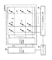
図1は、フォトセンサを構成する撮像部20とアドレス順次EL発光部10の構成を示す図である。図1(a)は、撮像部20とアドレス順次EL発光部10を上から見たときの構成を示す平面図である。図1(b)は、図1(a)のA−Aに沿って切断したときの断面の構成を示している。
【0019】
図1(a)、(b)に示すように、ガラス等で構成される基板1上には、撮像部20とアドレス順次EL発光部10との間に伸延して複数のアドレス導光路2が互いに実質的に平行に形成されている。アドレス導光路2は、アドレス順次EL発光部10で発せられた光を導き、光導電層23中に放射して撮像対象物に照射させる。
【0020】
アドレス順次EL発光部10は、アノード電極11と、有機EL(エレクトロルミネッセンス)層12と、カソード電極13と、封止膜14と、から構成される。
【0021】
アノード電極11は、ITO(Indium Tin Oxide)等で構成される透明電極である。そして、アノード電極11は、図1(a)に示すように、アドレス導光路2と同一本数形成され、図1(b)に示すように、アドレス導光路2の一端部上に形成される。
【0022】
有機EL層12は、アノード電極11の一部を覆うようにアドレス順次EL発光部10の全面に形成され、例えば、アノード電極11側に形成された正孔輸送層(図示せず)とカソード電極13側に形成された電子輸送性発光層(図示せず)とから構成される。正孔輸送層は、化学式1に示すα−NPDで形成される。
【0023】
【化1】

電子輸送性発光層は、化学式2に示すBebq2で形成される。
【0025】
【化2】
有機EL層12は、所定の電圧を印加されると所定の波長域の光を発光する。この場合、有機EL層12は緑色の波長域の光を発し、この波長域は、後述する撮像部20の光導電層23が有する分光感度特性に含まれるものとなる。この有機EL層12で発せられた光は、アドレス導光路2に入射され、アドレス導光路2中を伝わって、撮像部20中に放射される。
【0027】
カソード電極13は、MgAg、MgIn、AlLi等で形成された電極であり、有機EL層12上の全面に形成される。また、カソード電極13の電位は、ゼロとなるように接地されている。
【0028】
封止膜14は、有機EL層12、カソード電極13等への酸素又は水の浸入を防止するために、図1(b)に示すように、カソード電極13上に形成される。なお、封止膜14は、無機又は有機樹脂等を積層したものでもよい。
【0029】
撮像部20は、データ電極21と、遮光層22と、光導電層23と、透明電極24と、保護フィルム25と、から構成されている。
【0030】
遮光層22は、アドレス導光路2から伝搬される光を遮光する材料からなり、図1(a)に示すように、アドレス導光路2に対して実質的に垂直になるように、ある所定間隔で互いに実質的に平行に複数のアドレス導光路2にまたがって形成される。
【0031】
データ電極21は、図1(a)及び(b)に示すように、遮光層22上に形成される。ただし、アドレス導光路2から放射された光が、データ電極21の上部に直接入射しないようにするため、データ電極21は、図に示すように、遮光層22の幅よりも狭く形成される。また、データ電極21は、MgAg、MgIn、AlLi等で形成される。
【0032】
光導電層23は、図1(b)に示すように、アドレス導光路2、遮光層22、及び、データ電極21上に形成される。この光導電層23は、CdS(硫化カドミウム)や、化学式3に示すエオシン(eosine)を含むZnO(酸化亜鉛)等の、可視光線(波長:約400nm〜800nm)に分光感度特性を有する光導電物質である。
【0033】
【化3】
光導電層23では、可視光線(以下、単に「光」という)を吸収すると、光が吸収された箇所の内部にキャリア、即ち正孔と電子が生成される。従って、光が照射された箇所では、抵抗が小さくなる。一方、光導電層23の光が入射されない箇所は、抵抗値が高く、絶縁状態になっている。図1(b)からわかるように、アドレス導光路2から光が放射されたとき、その光は遮光層22によって妨げられるため、データ電極21の上部の光導電層23はアドレス導光路2からの光により直接導電性を示すことはない。
【0035】
透明電極24は、ITO等で形成された可視光を透過する電極であり、図1(b)に示すように、光導電層23上の全面に形成され接地されている。
【0036】
保護フィルム25は、透明のガラス、プラスチック等であり、透明電極24上に形成され、撮像部20を外部環境(ほこり等)から保護する。物体の像は、保護フィルム25を通して得られるので、200DPI以上の解像度を得る場合は、保護フィルム25の厚さは60μm以下であることが望ましい。
【0037】
以上に示したアドレス順次EL発光部10と撮像部20は、図1(b)に示すように、同一基板1上に形成され、アドレス導光路2でつながっているが、互いに離間した位置に形成されている。従って、高温等に弱い有機分子を用いた有機EL層12を、撮像部20を形成した後に形成する方が望ましい。
【0038】
なお、アドレス導光路2は、上記したように、アドレス順次EL発光部10で発せられた光を、撮像部20中に放射できるような屈折率を有する。すなわち、基板1の屈折率がアドレス導光路2の屈折率より小さく設定されているため、アドレス順次EL発光部10で発せられた光は、アドレス導光路2を透過し、アドレス導光路2中をほぼ反射しながら損失が少なく伝わり、撮像部20中では、アドレス導光路2の屈折率が光導電層23の屈折率と等しいか小さく設定されているため、アドレス導光路2と光導電層23との界面から光導電層23中に放射される。
【0039】
次に、上記の撮像部20とアドレス順次EL発光部10の駆動システムについて説明する。
【0040】
図2は、この駆動システムの構成を示す図である。
【0041】
アドレス順次EL発光部10と撮像部20の駆動システムは、図2に示すアドレスドライバ回路30と、データライン信号読み出し回路40と、コントロール部50と、から構成される。
【0042】
撮像部20の部分は、等価回路を示している。図中の破線は、アドレス導光路2を示しており、可変抵抗は、アドレス導光路2とデータ電極21とが交差する位置付近のデータ電極21上の光導電層23を示している。上記したように、光導電層23は、光が入射していない状態では絶縁状態になっているので、この可変抵抗の抵抗値は最大になっている。
【0043】
アドレスドライバ回路30は、複数のアノード電極11に接続され、コントロール部50からの制御信号に従って、アノード電極11に順次電圧を印加し、アドレス導光路2に選択的に光を入射させる。従って、アドレス導光路2は、一本ずつ選択されて、光を撮像部20中に放射する。
【0044】
データライン信号読み出し回路40は、複数のデータ電極21に接続され、コントロール部50からの制御信号に応答して、データ電極21をある一定の電位にする。上記したように、アドレス導光路2から選択されて放射された光は遮光層22によって遮られているので、この状態からは光導電層23の抵抗値は変化しない。しかし、撮像部20上に物体があり、この物体の光反射率が高いと、アドレス導光路2から放射された光は反射され、光導電層23に再入射する。この反射光は、いくらか角度を持って反射されているので、物体が存在する付近にある光導電層23(特にアドレス導光路2とデータ電極21とが交差する位置(この位置には、アドレス導光路2から直接光が放射されない))の抵抗値が局所的に低下する。
【0045】
例えば、可変抵抗Rの上部に光反射性の高い物体が存在すると、再入射した反射光によって抵抗Rの抵抗値が低下する。そして、この抵抗Rにつながっているデータ電極21では、蓄えられていた電荷が抵抗Rを通って透明電極24へ逃げて、その電位が変化する。データライン信号読み出し回路40は、このデータ電極21の電位変化も検出し、その検出結果を検出信号としてコントロール部50に出力する。
【0046】
コントロール部50は、後述する種々の制御信号を出力して、アドレスドライバ回路30とデータライン信号読み出し回路40の動作をコントロールする。
【0047】
次に、以上のような構成のフォトセンサの動作について、図3を参照して説明する。
【0048】
図3は、撮像部20上に撮像対象物(例えば、指紋)を置き、その像を読みとっている状態を示している。
【0049】
初めに、コントロール部50は、データライン信号読み出し回路40に、データ電極21を一定の電位(0V以外)にするよう命令する帯電信号を出力する。
【0050】
データライン信号読み出し回路40は、コントロール部50からの帯電信号に応答して、データ電極21を正又は負に帯電させる。
【0051】
次に、コントロール部50は、アドレス順次EL発光部10のアノード電極11に選択的に電圧を印加するよう、アドレスドライバ回路30に電圧印加信号を出力する。なお、アノード電極11への電圧印加は、一本ずつ順に行われる。
【0052】
アドレスドライバ回路30は、コントロール部50からの電圧印加信号に従って、アノード電極11に電圧を印加する。
【0053】
アドレス順次EL発光部10では、アノード電極11に電圧が印加されると、その部分の有機EL層12に、膜厚方向の電圧が印加される。従って、電圧が印加された部分の有機EL層12が発光する。
【0054】
有機EL層12が発光した光は、光が発光された部分にあるアドレス導光路2に入射される。
【0055】
アドレス導光路2に入射された光は、アドレス導光路2中を伝わりながら、撮像部20では、光導電層23との界面から光導電層23中に放射される。以上のようにして、アドレス導光路2は、一本ずつ選択され、光を光導電層23中に放射する。
【0056】
アドレス導光路2から選択されて放射された光は、撮像部20の遮光層22の間から、図3に示すように、光導電層23、透明電極24、及び、保護フィルム25を透過して、撮像対象物に照射される。
【0057】
撮像対象物が、例えば指紋の場合、この光は、指紋の凹部に対応する保護フィルム25の界面で反射され、撮像部20に再入射する。一方指紋の凸部に対応する保護フィルム25の界面では、光が指紋凸部を介して保護フィルム25から外に逃げるために対応するデータ電極21上の光導電層23にはほとんど入射されない。この反射光の入射強度は、図3に示すように、撮像対象物の形状、即ち、撮像対象物が保護フィルム25に接しているか否かということに応じて変化する。撮像対象物が保護フィルム25に接している部分では、光は効率よく反射されないが、保護フィルム25に接していない部分では、光は効率よく反射される。
【0058】
撮像対象物が保護フィルム25に接していない部分で反射された光は、撮像部20の光導電層23(特に、アドレス導光路2とデータ電極21とが交差する位置)に再入射する。
【0059】
アドレス導光路2とデータ電極21とが交差する位置における光導電層23で反射光が入射した部分では、上記したように、正孔−電子対が生成されるため、その部分の抵抗が小さくなる。従って、撮像対象物(指紋凹部)での反射光によって光導電層23の抵抗が小さくなった部分に相当するデータ電極21に蓄えられている電荷が光導電層23を通って透明電極24に流れ、そのデータ電極21の電位が変化する。
【0060】
データライン信号読み出し回路40は、コントロール部50からの制御信号に従ってデータ電極21の電位変化を検出し、検出信号としてコントロール部50に出力する。
【0061】
コントロール部50は、データライン信号読み出し回路40から入力された検出信号をデータとして蓄積する。
【0062】
そして、コントロール部50は、次の行のアドレス導光路2を発光させて撮像するために、データライン信号読み出し回路40に帯電信号を出力する。
【0063】
以後の動作は、上記と同様である。また、以上の動作は、アドレス順次EL発光部10のアノード電極11に、順に電圧を印加していき、全てのアノード電極11に電圧が印加されるまで繰り返される。即ち、アドレス導光路2に順に光が入射され、全てのアドレス導光路2に光が入射されるまで繰り返される。そして、蓄積された撮像対象物の像は、像の再生や照合に使用される。
【0064】
次に、以上に示した処理によって得られる像について、図4を用いて、説明する。
【0065】
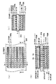
図4は、撮像部20上にドーナツ状の凹部を有し、凹部以外が平坦である物体が載置された状態を示している。
【0066】
撮像部20を通っているアドレス導光路2とデータ電極21は、図4に示すように、それぞれ、11本(A1〜A11)、13本(D1〜D13)あるとする。また、物体の底面は撮像部20の保護フィルム25に接触しているとする。従って、物体の凹部により保護フィルム25に接触していない部分に対応するアドレス導光路2とデータ電極21との交点は、図4の丸で囲んだ点である。
【0067】
初めに、データライン信号読み出し回路40が、データ電極21を帯電させる。撮像部20の光導電層23にはまだ光が入射していないので、光導電層23は、絶縁状態である。
【0068】
次に、アドレスドライバ回路30が、順にアノード電極11に電圧を印加する。これにより、有機EL層12が発光し、順にアドレス導光路2に光が入射される。
【0069】
アドレス導光路2から放射された光が、撮像対象物の凹部によって保護フィルム25で反射されて撮像部20に再入射すると、その部分の光導電層23の抵抗が小さくなる。図4では、アドレス導光路A3が光を放射したとき、物体の凹部が存在する部分に相当する光導電層23の部分、即ちアドレス導光路A3のA3−1からA3−2に相当する部分近傍の光導電層23の抵抗が小さくなる。
【0070】
この抵抗値の低下によって、データ電極21に蓄えられている電荷は、光導電層23の抵抗値が低下した部分を通って透明電極24から逃げていく。従って、撮像対象物が接触していない部分に相当するデータ電極21の電位が変化する。即ち、データ電極D6、D7、及び、D8の電位が変化する。
【0071】
コントロール部50は、アドレス導光路A3に光を入射するようにアドレスドライバ回路30に電圧印加信号を出力し、また、データライン信号読み出し回路40から、データ電極D6、D7、及び、D8の電位が低下したという検出信号を受け取る。従って、コントロール部50は、例えば、(A3,D6)、(A3,D7)、(A3,D8)というようにして、物体が存在しない部分に対応する点(図4の点a、b、c)をデータとして蓄積することができる。
【0072】
アドレス導光路A11まで光が入射されると、物体が接触していない部分に対応する点(図4で、丸で囲んだ点)が、データとして蓄積される。
【0073】
このデータを使用して、例えば、データ電極のD1からD13をX座標、アドレス導光路のA1からA11をY座標にすれば、図4の丸で囲んだ点が、図5のように再現される。この再現像は、アドレス導光路2とデータ電極21の本数を増やし、点の数を多くすることによって、より正確に物体の像を表すことができる。このアドレス導光路2とデータ電極21の本数は、撮像の目的に応じて、実験等によって決定される。
【0074】
以上のようにアドレス導光路2とデータ電極21を目的に応じて設定し、それに伴ってアノード電極11と遮光層22を微細加工しておけば、光導電層23、透明電極24、有機EL層12、及び、カソード電極13をパターニングする必要がなくなる。また、基板1に高融点ガラスを使用する必要もなくなり、撮像部20の生産コストを低減することができる。
【0075】
また、上記したように、有機EL層12によって発せられた光がアドレス導光路2を介して撮像対象物に照射されるので、直角プリズム等を使用する必要がなくなり、フォトセンサ全体を薄型に構成することができる。
【0076】
また、以上のようにして得られる物体の形状をデータとして予めメモリ等に記憶しておき、撮像で得られた物体の形状が、メモリ内のデータに合うか否かということを判定することもできる。これは、例えば、指紋の照合等に応用できる。
【0077】
次に、本発明の第2の実施の形態にかかるフォトセンサについて説明する。
【0078】
このフォトセンサは、第1の実施の形態で示したフォトセンサのアドレス順次EL発光部10が、基板を挟んで撮像部20と対向するような構成になっている。
【0079】
図6は、このフォトセンサの構成を示す図である。図6(a)は、フォトセンサを上から見た平面図である。図6(b)は、(a)のフォトセンサをB−Bで切断したときの断面の構造を示している。図6(c)は、(a)のフォトセンサをC−Cで切断したときの断面の構造を示している。また、図中で参照番号が図1中の番号と同じものは、図1と同じものを示す。
【0080】
このフォトセンサが、第1の実施の形態で示したフォトセンサと大きく異なる点は、アドレス導光路を使用せず、ルーバー基板4を用い、撮像部20が形成されている面と異なる面に、アノード電極11’、有機EL層12’、カソード電極13’及び封止膜14’から成るアドレス順次EL発光部10’が形成されていることである。
【0081】
ルーバー基板4は、アノード電極11’に沿って設けられたアドレス光に対し透過率の高い導光部4aと導光部4aの両側をアドレス光に対し高い反射性を示す反射部4bを有する。したがって、複数のうち所定のアノード電極11’から入射された光は、ルーバー基板4の複数の導光部4aのうちの所定ものにのみ入射され、そのまま導光部4aのみを透過し光導電層23に向けて直進するか、反射部4bで反射を繰り返してほぼ進行方向が直進方向に制御されてから導光部4aから光導電層23に向けて出射される。
【0082】
複数のアノード電極11’には、第1の実施の形態と同様に、一つずつ順に電圧が印加される。なお、アノード電極11’は、図6に示すように、実質的にデータ電極21に直交するように、互いに平行に形成されている。
【0083】
そして、アノード電極11’へ所定の電圧を印加することによって有機EL層12’で発せられた光は、ルーバー基板4の反射部4b間で反射され、隣に漏れることはないので、実質的にアドレス導光路2と同様の機能を果たすことになる。
【0084】
これ以外の部分の機能や動作、その駆動システムや撮像方法は、第1の実施の形態で示したのと実質的に同様である。
【0085】
以上のように有機EL層12’とデータ電極21を目的に応じて設定し、それに伴ってアノード電極11’と遮光層22を微細加工しておけば、光導電層23、透明電極24、有機EL層12’、及び、カソード電極13’をパターニングする必要がなくなる。また、基板に高融点ガラスを使用する必要もなくなり、フォトセンサの生産コストを低減することができる。
【0086】
また、上記したように、有機EL層12’によって発せられた光が直接、撮像対象物に照射されるので、直角プリズム等を使用する必要がなくなり、フォトセンサ全体を薄型に構成することができる。
【0087】
本発明は、上記の第1、第2の実施の形態に限られず、種々の変形、応用が可能である。以下、本発明に適用可能な上記の実施の形態の変形態様について、説明する。
【0088】
第1の実施の形態で示したアドレス導光路2は、基板に溝等を形成し、この溝を導光路としてもよい。
【0089】
また、光導電層23は、画素(アドレス導光路2又はアノード電極11’とデータ電極21との交点)に応じて島状、又は、図7に示すように、データ電極21より狭い幅で、ライン状に形成してもよい。このようにすると、データ電極21によって、アドレス導光路2から光導電層23に入射する光が妨げられるので、遮光層22を省くことができる。この場合、光導電層23の間は、光を透過する層間絶縁樹脂27で形成される。
【0090】
さらに、保護フィルム25は、薄膜フィルムとしてもよい。この場合は、光導電層23が外部環境に対して強いものとなる。
【0091】
また、透明電極24及びカソード電極13は、一枚でなく、それぞれデータ電極21とアノード電極11に対応するように、同じパターンで形成されてもよい。さらに、透明電極24は、画素(アドレス導光路2又はアノード電極11’とデータ電極21との交点)に対応する位置にのみ形成されてもよい。
【0092】
第2の実施の形態で示した基板(ルーバー基板4)は、ルーバー基板を備えたガラス基板でもよく、ルーバー基板の代わりに光ファイバプレートを薄く切り出した基板でもよい。光ファイバプレートは、長尺方向がアノード電極11’と光導電層23とを結ぶ最短の線分の方向に実質的に等しい透明な複数のファイバが束になった状態で光反射性のハニカム形状の筒内に収容された構造であり、アノード電極11’から入射された光が光導電層23に向けて進行するように設定されている。
【0093】
また、フォトセンサは、撮像部20の光導電層23に入射する反射光量の違いによる、光導電層23の抵抗値の変化を利用しているので、撮像対象物は、指紋のように凹凸のある物だけでなく、反射率の異なるものであれば何でもよい。例えば、白い紙の上に黒で書かれた像では、その白の部分と黒の部分の反射率は異なるので、その像を上記の方法で読みとることができる。従って、以上で示したフォトセンサは、スキャナとしても使用できる。
【0094】
さらに、以上で示したフォトセンサで、光の入射に対してその抵抗値が緩やかに変化する光導電層23を使用し、予め入射光量に対する抵抗値の時間変化等がわかっている場合は、データ電極21の電位を時間のタイミングを取って計測することによって、撮像対象物の階調を読むことができる。また、光導電層23にこのようなものが適用できる場合には、カーボンブラックのようにデータ電極21が光に対して非透過性を有すれば、これが遮光層22を兼ねることができる。
【0095】
また、第1の実施の形態で示した撮像部20は、基板1上に透明電極24、光導電層23が順に積層されて形成され、光導電層23上にデータ電極21、遮光層22が形成され、その上に保護フィルム25が積層されて形成された構成にしてもよい。この場合は、光を保護フィルム25から基板1の方向に入射し、撮像対象物を基板1の表面に接触させるようにする。
【0096】
【発明の効果】
以上の説明から明らかなように、本発明により、撮像装置に直角プリズムを使用する必要がなくなる。また、発光層や導電層で複雑なパターニングを行う必要がない。
【0097】
従って、良好な撮像を行い、生産コストを低減した撮像素子を提供することができる。
【図面の簡単な説明】
【図1】第1の実施の形態にかかるフォトセンサの撮像部とアドレス順次EL発光部の構成を示す図である。
【図2】撮像部とアドレス順次EL発光部の駆動システムを示す図である。
【図3】撮像対象物の像を撮像している状態を示す図である。
【図4】撮像対象物を読みとるときの動作を説明するための図である。
【図5】撮像のデータを再現した状態を示す図である。
【図6】第2の実施の形態にかかるフォトセンサの構成を示す図である。
【図7】撮像部の光導電層の他の構成を示す図である。
【図8】従来の撮像装置の構成例を示す図である。
【符号の説明】
1・・・基板、2・・・アドレス導光路、4・・・ルーバー基板、4a・・・導光部、4b・・・反射部、10・・・アドレス順次EL発光部、11・・・アノード電極、12・・・有機EL層、13・・・カソード電極、14・・・封止膜、10’・・・アドレス順次EL発光部、11’・・・アノード電極、12’・・・有機EL層、13’・・・カソード電極、14’・・・封止膜、20・・・撮像部、21・・・データ電極、22・・・遮光層、23・・・光導電層、24・・・透明電極、25・・・保護フィルム、27・・・層間絶縁樹脂、30・・・アドレスドライバ回路、40・・・データライン信号読み出し回路、50・・・コントロール部、60・・・直角プリズム、60a・・・全反射フィルム、61・・・光源、62・・・レンズ、63・・・CCD、FG・・・指[0001]
BACKGROUND OF THE INVENTION
The present invention relates to an image sensor that reads an image of an object, and more particularly to an image sensor that reads an image of an object using light.
[0002]
[Prior art]
A fingerprint sensor is known as an imaging device that reads an image of an object using light.
[0003]
The fingerprint has a shape unique to each individual, and since it is easy to perform collation by pattern matching, the fingerprint sensor is widely used to identify a specific individual.
[0004]
An example of a fingerprint sensor using a CCD (Charge Coupled Device) as an image pickup element that reads an object image is shown in FIG.
[0005]
The fingerprint sensor shown in FIG. 8 includes a right-
[0006]
In this state, the light incident on the right-
[0007]
In addition, as an imaging device other than the above, there is an imaging device that uses a double-gate TFT (Thin Film Transistor) instead of a CCD as an imaging device.
[0008]
In a two-dimensional imaging device using such a TFT, the TFT is assembled in an XY matrix array, and image information for each pixel is read from the data line.
[0009]
[Problems to be solved by the invention]
However, in the above-described fingerprint sensor, it is necessary to change the angle of light from the
[0010]
On the other hand, an imaging device using a TFT with a double gate structure has a problem that the production cost is high because refractory glass is used for the substrate and CVD (Chemical Vapor Deposition) is performed for element formation. .
[0011]
Accordingly, an object of the present invention is to provide an image pickup device capable of forming the entire apparatus thin.
[0012]
[Means for Solving the Problems]
In order to achieve the above object, an imaging device according to a first aspect of the present invention includes a plurality of light guides that are spaced apart from each other and formed substantially in parallel and guide incident light, and the plurality of light guides. A plurality of light emitting elements that are formed corresponding to each of the optical paths, emit light according to an applied voltage, and guide the light to each of the plurality of light guide paths; And a plurality of first electrodes formed at positions where the plurality of light guides form a predetermined angle and the plurality of light emitting elements are not formed, at least the plurality of light guides and the plurality of firsts. The photoconductive layer is formed by laminating with the first electrode at the position of the intersection with the electrode, and changes its resistance value when light in a predetermined wavelength region is incident on the photoconductive layer. Light blocking means for blocking the light so that the emitted light does not enter directly; Characterized in that it comprises a second electrode formed by laminating the photoconductive layer opposite to the plurality of first electrodes corresponding to the position where the photoconductive layer is formed.
[0013]
According to the present invention, it is possible to irradiate light on an imaging object, and to detect the shape and shading of the imaging object by a change in the resistance value of the photoconductive layer due to light reflected according to the imaging object. Can do. Moreover, the light with which the imaging object is irradiated may be guided from the corresponding light emitting element through a plurality of light guide paths. Therefore, in an imaging apparatus to which this imaging element is applied, it is not necessary to use a right-angle prism or the like, and the entire imaging apparatus can be configured to be thin.
[0014]
Further, if the light guide path and the first or second electrode are finely configured, the photoconductive layer need not be subjected to a process such as photolithography or etching to be complicatedly patterned. Accordingly, the production cost of the imaging device can be reduced.
[0015]
The light emitting element and the photoconductive layer may be spaced apart so as not to overlap each other in the layer thickness direction.
[0016]
The plurality of first electrodes may be made of a material that does not transmit light, and may be formed between the photoconductive layer and the plurality of light guides, and may also serve as the light blocking unit. .
[0017]
DETAILED DESCRIPTION OF THE INVENTION
Hereinafter, the photosensor according to the first embodiment of the present invention will be described.
[0018]
FIG. 1 is a diagram illustrating a configuration of an imaging unit 20 and an address sequential EL
[0019]
As shown in FIGS. 1A and 1B, a plurality of address light guides 2 extending between the imaging unit 20 and the address sequential EL
[0020]
The address sequential EL
[0021]
The
[0022]
The organic EL layer 12 is formed on the entire surface of the address sequential EL
[0023]
[Chemical 1]
The electron-transporting light-emitting layer is formed of Bebq2 shown in Chemical Formula 2.
[0025]
[Chemical formula 2]
The organic EL layer 12 emits light in a predetermined wavelength region when a predetermined voltage is applied. In this case, the organic EL layer 12 emits light in the green wavelength range, and this wavelength range is included in the spectral sensitivity characteristics of the
[0027]
The cathode electrode 13 is an electrode formed of MgAg, MgIn, AlLi or the like, and is formed on the entire surface of the organic EL layer 12. The potential of the cathode electrode 13 is grounded so as to be zero.
[0028]
The sealing film 14 is formed on the cathode electrode 13 as shown in FIG. 1B in order to prevent oxygen or water from entering the organic EL layer 12, the cathode electrode 13, and the like. The sealing film 14 may be a laminate of inorganic or organic resins.
[0029]
The imaging unit 20 includes a
[0030]
The light shielding layer 22 is made of a material that shields light propagating from the address light guide 2 and has a predetermined interval so as to be substantially perpendicular to the address light guide 2 as shown in FIG. Are formed across a plurality of address light guide paths 2 substantially parallel to each other.
[0031]
The
[0032]
As shown in FIG. 1B, the
[0033]
[Chemical 3]
In the
[0035]
The
[0036]
The protective film 25 is made of transparent glass, plastic, or the like, and is formed on the
[0037]
As shown in FIG. 1B, the address sequential EL
[0038]
Note that the address light guide 2 has a refractive index that allows the light emitted from the address sequential EL
[0039]
Next, a driving system for the imaging unit 20 and the address sequential EL
[0040]
FIG. 2 is a diagram showing the configuration of this drive system.
[0041]
The drive system for the address sequential EL
[0042]
The part of the imaging unit 20 shows an equivalent circuit. The broken line in the figure indicates the address light guide 2, and the variable resistor indicates the
[0043]
The
[0044]
The data line
[0045]
For example, when an object having high light reflectivity exists above the variable resistor R, the resistance value of the resistor R is lowered by the re-incident reflected light. In the
[0046]
The
[0047]
Next, the operation of the photosensor having the above configuration will be described with reference to FIG.
[0048]
FIG. 3 shows a state where an imaging object (for example, a fingerprint) is placed on the imaging unit 20 and the image is read.
[0049]
First, the
[0050]
The data line
[0051]
Next, the
[0052]
The
[0053]
In the address sequential EL
[0054]
The light emitted from the organic EL layer 12 enters the address light guide path 2 in the portion where the light is emitted.
[0055]
The light incident on the address light guide 2 is radiated into the
[0056]
The light selected and emitted from the address light guide path 2 passes through the
[0057]
When the imaging target is a fingerprint, for example, this light is reflected at the interface of the protective film 25 corresponding to the concave portion of the fingerprint and re-enters the imaging unit 20. On the other hand, at the interface of the protective film 25 corresponding to the convex portion of the fingerprint, light escapes from the protective film 25 through the fingerprint convex portion, so that it hardly enters the
[0058]
The light reflected by the part where the imaging object is not in contact with the protective film 25 reenters the
[0059]
In the portion where the reflected light is incident on the
[0060]
The data line
[0061]
The
[0062]
Then, the
[0063]
The subsequent operation is the same as described above. Further, the above operation is repeated until voltage is applied to the
[0064]
Next, an image obtained by the processing described above will be described with reference to FIG.
[0065]
FIG. 4 shows a state in which an object having a donut-shaped recess on the imaging unit 20 and a flat surface other than the recess is placed.
[0066]
As shown in FIG. 4, it is assumed that there are 11 (A1 to A11) and 13 (D1 to D13) address light guide paths 2 and
[0067]
First, the data line
[0068]
Next, the
[0069]
When the light radiated from the address light guide path 2 is reflected by the protective film 25 by the concave portion of the imaging target and re-enters the imaging unit 20, the resistance of the
[0070]
Due to the decrease in the resistance value, the charge stored in the
[0071]
The
[0072]
When light enters the address light guide A11, points corresponding to portions where the object is not in contact (dotted points in FIG. 4) are accumulated as data.
[0073]
Using this data, for example, if D1 to D13 of the data electrode are set to the X coordinate and A1 to A11 of the address light guide are set to the Y coordinate, the circled points in FIG. 4 are reproduced as shown in FIG. The This redevelopment can more accurately represent the image of the object by increasing the number of address light guides 2 and
[0074]
As described above, if the address light guide 2 and the
[0075]
In addition, as described above, the light emitted from the organic EL layer 12 is irradiated onto the object to be imaged via the address light guide path 2, so that it is not necessary to use a right-angle prism or the like, and the entire photosensor is configured to be thin. can do.
[0076]
In addition, the shape of the object obtained as described above may be stored in advance in a memory or the like as data, and it may be determined whether or not the shape of the object obtained by imaging matches the data in the memory. it can. This can be applied to, for example, fingerprint verification.
[0077]
Next, a photosensor according to a second embodiment of the present invention will be described.
[0078]
This photosensor is configured such that the address sequential EL
[0079]
FIG. 6 is a diagram showing the configuration of this photosensor. FIG. 6A is a plan view of the photosensor as viewed from above. FIG. 6B shows a cross-sectional structure when the photosensor of FIG. FIG. 6C shows a cross-sectional structure when the photosensor of FIG. Also, the same reference numerals in FIG. 1 as those in FIG. 1 indicate the same elements as in FIG.
[0080]
The difference between this photosensor and the photosensor shown in the first embodiment is that the address light guide is not used, the
[0081]
The
[0082]
As in the first embodiment, voltages are sequentially applied to the plurality of
[0083]
The light emitted from the organic EL layer 12 ′ by applying a predetermined voltage to the
[0084]
The functions and operations of other parts, the driving system and the imaging method are substantially the same as those described in the first embodiment.
[0085]
As described above, if the organic EL layer 12 ′ and the
[0086]
Further, as described above, the light emitted from the organic EL layer 12 ′ is directly applied to the imaging target, so that it is not necessary to use a right-angle prism or the like, and the entire photosensor can be configured to be thin. .
[0087]
The present invention is not limited to the first and second embodiments described above, and various modifications and applications are possible. Hereinafter, modifications of the above-described embodiment applicable to the present invention will be described.
[0088]
In the address light guide 2 shown in the first embodiment, a groove or the like may be formed in the substrate, and this groove may be used as the light guide.
[0089]
Further, the
[0090]
Furthermore, the protective film 25 may be a thin film. In this case, the
[0091]
Further, the
[0092]
The substrate (louver substrate 4) shown in the second embodiment may be a glass substrate provided with a louver substrate, or a substrate obtained by thinly cutting an optical fiber plate instead of the louver substrate. The optical fiber plate has a light-reflective honeycomb shape in which a plurality of transparent fibers whose length direction is substantially equal to the direction of the shortest line segment connecting the
[0093]
In addition, since the photosensor uses a change in the resistance value of the
[0094]
Furthermore, in the photosensor described above, when the
[0095]
The imaging unit 20 shown in the first embodiment is formed by sequentially laminating a
[0096]
【The invention's effect】
As is apparent from the above description, the present invention eliminates the need to use a right-angle prism in the imaging device. Further, it is not necessary to perform complicated patterning on the light emitting layer or the conductive layer.
[0097]
Therefore, it is possible to provide an imaging device that performs favorable imaging and reduces production costs.
[Brief description of the drawings]
FIG. 1 is a diagram illustrating a configuration of an imaging unit and an address sequential EL light emitting unit of a photosensor according to a first embodiment.
FIG. 2 is a diagram illustrating a driving system for an imaging unit and an address sequential EL light emitting unit.
FIG. 3 is a diagram illustrating a state in which an image of an imaging target is being captured.
FIG. 4 is a diagram for explaining an operation when reading an imaging object;
FIG. 5 is a diagram illustrating a state in which imaging data is reproduced.
FIG. 6 is a diagram illustrating a configuration of a photosensor according to a second embodiment.
FIG. 7 is a diagram illustrating another configuration of the photoconductive layer of the imaging unit.
FIG. 8 is a diagram illustrating a configuration example of a conventional imaging device.
[Explanation of symbols]
DESCRIPTION OF SYMBOLS 1 ... Board | substrate, 2 ... Address light guide path, 4 ... Louver board, 4a ... Light guide part, 4b ... Reflection part, 10 ... Address sequential EL light emission part, 11 ... Anode electrode, 12 ... organic EL layer, 13 ... cathode electrode, 14 ... sealing film, 10 '... address sequential EL light emitting part, 11' ... anode electrode, 12 '... Organic EL layer, 13 '... cathode electrode, 14' ... sealing film, 20 ... imaging part, 21 ... data electrode, 22 ... light shielding layer, 23 ... photoconductive layer, 24 ... Transparent electrode, 25 ... Protective film, 27 ... Interlayer insulating resin, 30 ... Address driver circuit, 40 ... Data line signal readout circuit, 50 ... Control unit, 60 ... Right angle prism, 60a ... Total reflection film, 61 ... Light source, 62 ... Lens, 63 ··· CCD, FG ··· finger
Claims (3)
前記複数の導光路のそれぞれの一部に対応して形成され、印加された電圧に応じて発光し、前記複数の導光路のそれぞれに光を導く複数の発光素子と、
互いに離間されて実質的に平行に、かつ前記複数の導光路と所定の角度をなし、前記複数の発光素子が形成されていない位置に形成されている複数の第1の電極と、
少なくとも前記複数の導光路と前記複数の第1の電極との交点の位置に前記第1の電極と積層して形成され、所定の波長域の光が入射されると抵抗値が変化する光導電層と、
前記光導電層に、前記導光路から出射された光が直接入射しないように、光を遮る光遮断手段と、
前記光導電層が形成されている位置に対応して前記複数の第1の電極と対向して前記光導電層に積層して形成された第2の電極と、
を備えることを特徴とする撮像素子。A plurality of light guides that are spaced apart from each other and formed substantially parallel to guide incident light;
A plurality of light emitting elements formed corresponding to each of the plurality of light guide paths, emitting light according to an applied voltage, and guiding light to each of the plurality of light guide paths;
A plurality of first electrodes that are spaced apart from each other and substantially parallel to each other, form a predetermined angle with the plurality of light guide paths, and are formed at positions where the plurality of light emitting elements are not formed;
A photoconductive layer formed by laminating with the first electrode at least at the intersection of the plurality of light guides and the plurality of first electrodes, and having a resistance value that changes when light in a predetermined wavelength region is incident. Layers,
Light blocking means for blocking light so that light emitted from the light guide does not directly enter the photoconductive layer;
A second electrode formed by laminating the photoconductive layer so as to face the plurality of first electrodes corresponding to the position where the photoconductive layer is formed;
An image pickup device comprising:
Priority Applications (1)
| Application Number | Priority Date | Filing Date | Title |
|---|---|---|---|
| JP27249298A JP3975579B2 (en) | 1998-09-10 | 1998-09-10 | Image sensor |
Applications Claiming Priority (1)
| Application Number | Priority Date | Filing Date | Title |
|---|---|---|---|
| JP27249298A JP3975579B2 (en) | 1998-09-10 | 1998-09-10 | Image sensor |
Publications (2)
| Publication Number | Publication Date |
|---|---|
| JP2000090251A JP2000090251A (en) | 2000-03-31 |
| JP3975579B2 true JP3975579B2 (en) | 2007-09-12 |
Family
ID=17514678
Family Applications (1)
| Application Number | Title | Priority Date | Filing Date |
|---|---|---|---|
| JP27249298A Expired - Fee Related JP3975579B2 (en) | 1998-09-10 | 1998-09-10 | Image sensor |
Country Status (1)
| Country | Link |
|---|---|
| JP (1) | JP3975579B2 (en) |
Families Citing this family (2)
| Publication number | Priority date | Publication date | Assignee | Title |
|---|---|---|---|---|
| JP2003233805A (en) | 2001-12-04 | 2003-08-22 | Canon Inc | Image input device |
| JP4844481B2 (en) * | 2007-06-25 | 2011-12-28 | 株式会社日立製作所 | Imaging apparatus and apparatus equipped with the same |
-
1998
- 1998-09-10 JP JP27249298A patent/JP3975579B2/en not_active Expired - Fee Related
Also Published As
| Publication number | Publication date |
|---|---|
| JP2000090251A (en) | 2000-03-31 |
Similar Documents
| Publication | Publication Date | Title |
|---|---|---|
| US10990789B2 (en) | Display apparatus including light-receiving pixel area | |
| CN112242421B (en) | Electroluminescent devices | |
| US10339359B2 (en) | Display panel and display device | |
| CN110649065B (en) | Display device with built-in optical image sensor | |
| CN108121483B (en) | Flat panel display with embedded optical imaging sensor | |
| US10990794B2 (en) | Operation method of texture recognition device and texture recognition device | |
| KR102040651B1 (en) | Flat Panel Display Embedding Optical Imaging Sensor | |
| US20100155578A1 (en) | Light source integrated photoelectric conversion apparatus | |
| JP3704889B2 (en) | Display device | |
| EP3885800B1 (en) | Display device | |
| CN112236774A (en) | Texture recognition device and driving method of the texture recognition device | |
| CN109840464B (en) | Electronic panel and electronic device including the electronic panel | |
| KR102901341B1 (en) | Display device | |
| KR20180117748A (en) | Transparent Fingerprint Image Scanning Panel and Display Apparatus Comprising The Same | |
| KR102636405B1 (en) | Display apparatus including light rpceving pixel area | |
| CN113853610A (en) | Texture recognition device and opposite substrate | |
| EP4145341B1 (en) | Optical sensor array substrate and optical fingerprint collector | |
| WO2020232637A1 (en) | Texture recognition apparatus and manufacturing method therefor and colour film substrate and manufacturing method therefor | |
| JP3975579B2 (en) | Image sensor | |
| CN111898397B (en) | Texture recognition device | |
| KR20200046817A (en) | Display apparatus including light receving pixel area | |
| US11200397B2 (en) | Fingerprint identification assembly, display substrate, display panel and fingerprint identification method | |
| CN114284319B (en) | Display panels and electronic equipment | |
| JP2000341472A (en) | Imaging device and method of manufacturing the same | |
| CN111650769A (en) | A display device and a driving method thereof |
Legal Events
| Date | Code | Title | Description |
|---|---|---|---|
| A621 | Written request for application examination |
Free format text: JAPANESE INTERMEDIATE CODE: A621 Effective date: 20040414 |
|
| A977 | Report on retrieval |
Free format text: JAPANESE INTERMEDIATE CODE: A971007 Effective date: 20070515 |
|
| TRDD | Decision of grant or rejection written | ||
| A01 | Written decision to grant a patent or to grant a registration (utility model) |
Free format text: JAPANESE INTERMEDIATE CODE: A01 Effective date: 20070529 |
|
| A61 | First payment of annual fees (during grant procedure) |
Free format text: JAPANESE INTERMEDIATE CODE: A61 Effective date: 20070611 |
|
| FPAY | Renewal fee payment (event date is renewal date of database) |
Free format text: PAYMENT UNTIL: 20100629 Year of fee payment: 3 |
|
| R150 | Certificate of patent or registration of utility model |
Free format text: JAPANESE INTERMEDIATE CODE: R150 |
|
| FPAY | Renewal fee payment (event date is renewal date of database) |
Free format text: PAYMENT UNTIL: 20110629 Year of fee payment: 4 |
|
| FPAY | Renewal fee payment (event date is renewal date of database) |
Free format text: PAYMENT UNTIL: 20110629 Year of fee payment: 4 |
|
| FPAY | Renewal fee payment (event date is renewal date of database) |
Free format text: PAYMENT UNTIL: 20120629 Year of fee payment: 5 |
|
| LAPS | Cancellation because of no payment of annual fees |