JP3974305B2 - Etching agent, method for manufacturing electronic device substrate using the same, and electronic device - Google Patents
Etching agent, method for manufacturing electronic device substrate using the same, and electronic device Download PDFInfo
- Publication number
- JP3974305B2 JP3974305B2 JP2000001127A JP2000001127A JP3974305B2 JP 3974305 B2 JP3974305 B2 JP 3974305B2 JP 2000001127 A JP2000001127 A JP 2000001127A JP 2000001127 A JP2000001127 A JP 2000001127A JP 3974305 B2 JP3974305 B2 JP 3974305B2
- Authority
- JP
- Japan
- Prior art keywords
- film
- etching
- laminated
- etching agent
- substrate
- Prior art date
- Legal status (The legal status is an assumption and is not a legal conclusion. Google has not performed a legal analysis and makes no representation as to the accuracy of the status listed.)
- Expired - Lifetime
Links
Images


Classifications
-
- C—CHEMISTRY; METALLURGY
- C23—COATING METALLIC MATERIAL; COATING MATERIAL WITH METALLIC MATERIAL; CHEMICAL SURFACE TREATMENT; DIFFUSION TREATMENT OF METALLIC MATERIAL; COATING BY VACUUM EVAPORATION, BY SPUTTERING, BY ION IMPLANTATION OR BY CHEMICAL VAPOUR DEPOSITION, IN GENERAL; INHIBITING CORROSION OF METALLIC MATERIAL OR INCRUSTATION IN GENERAL
- C23F—NON-MECHANICAL REMOVAL OF METALLIC MATERIAL FROM SURFACE; INHIBITING CORROSION OF METALLIC MATERIAL OR INCRUSTATION IN GENERAL; MULTI-STEP PROCESSES FOR SURFACE TREATMENT OF METALLIC MATERIAL INVOLVING AT LEAST ONE PROCESS PROVIDED FOR IN CLASS C23 AND AT LEAST ONE PROCESS COVERED BY SUBCLASS C21D OR C22F OR CLASS C25
- C23F1/00—Etching metallic material by chemical means
- C23F1/10—Etching compositions
- C23F1/14—Aqueous compositions
- C23F1/16—Acidic compositions
- C23F1/18—Acidic compositions for etching copper or alloys thereof
-
- H—ELECTRICITY
- H10—SEMICONDUCTOR DEVICES; ELECTRIC SOLID-STATE DEVICES NOT OTHERWISE PROVIDED FOR
- H10D—INORGANIC ELECTRIC SEMICONDUCTOR DEVICES
- H10D30/00—Field-effect transistors [FET]
- H10D30/60—Insulated-gate field-effect transistors [IGFET]
- H10D30/67—Thin-film transistors [TFT]
-
- C—CHEMISTRY; METALLURGY
- C23—COATING METALLIC MATERIAL; COATING MATERIAL WITH METALLIC MATERIAL; CHEMICAL SURFACE TREATMENT; DIFFUSION TREATMENT OF METALLIC MATERIAL; COATING BY VACUUM EVAPORATION, BY SPUTTERING, BY ION IMPLANTATION OR BY CHEMICAL VAPOUR DEPOSITION, IN GENERAL; INHIBITING CORROSION OF METALLIC MATERIAL OR INCRUSTATION IN GENERAL
- C23F—NON-MECHANICAL REMOVAL OF METALLIC MATERIAL FROM SURFACE; INHIBITING CORROSION OF METALLIC MATERIAL OR INCRUSTATION IN GENERAL; MULTI-STEP PROCESSES FOR SURFACE TREATMENT OF METALLIC MATERIAL INVOLVING AT LEAST ONE PROCESS PROVIDED FOR IN CLASS C23 AND AT LEAST ONE PROCESS COVERED BY SUBCLASS C21D OR C22F OR CLASS C25
- C23F1/00—Etching metallic material by chemical means
- C23F1/10—Etching compositions
- C23F1/14—Aqueous compositions
- C23F1/16—Acidic compositions
- C23F1/26—Acidic compositions for etching refractory metals
-
- H—ELECTRICITY
- H10—SEMICONDUCTOR DEVICES; ELECTRIC SOLID-STATE DEVICES NOT OTHERWISE PROVIDED FOR
- H10P—GENERIC PROCESSES OR APPARATUS FOR THE MANUFACTURE OR TREATMENT OF DEVICES COVERED BY CLASS H10
- H10P14/00—Formation of materials, e.g. in the shape of layers or pillars
- H10P14/40—Formation of materials, e.g. in the shape of layers or pillars of conductive or resistive materials
- H10P14/418—Formation of materials, e.g. in the shape of layers or pillars of conductive or resistive materials the conductive layers comprising transition metals
-
- H—ELECTRICITY
- H10—SEMICONDUCTOR DEVICES; ELECTRIC SOLID-STATE DEVICES NOT OTHERWISE PROVIDED FOR
- H10P—GENERIC PROCESSES OR APPARATUS FOR THE MANUFACTURE OR TREATMENT OF DEVICES COVERED BY CLASS H10
- H10P50/00—Etching of wafers, substrates or parts of devices
- H10P50/60—Wet etching
- H10P50/66—Wet etching of conductive or resistive materials
- H10P50/663—Wet etching of conductive or resistive materials by chemical means only
- H10P50/667—Wet etching of conductive or resistive materials by chemical means only by liquid etching only
-
- H—ELECTRICITY
- H10—SEMICONDUCTOR DEVICES; ELECTRIC SOLID-STATE DEVICES NOT OTHERWISE PROVIDED FOR
- H10W—GENERIC PACKAGES, INTERCONNECTIONS, CONNECTORS OR OTHER CONSTRUCTIONAL DETAILS OF DEVICES COVERED BY CLASS H10
- H10W20/00—Interconnections in chips, wafers or substrates
- H10W20/40—Interconnections external to wafers or substrates, e.g. back-end-of-line [BEOL] metallisations or vias connecting to gate electrodes
- H10W20/41—Interconnections external to wafers or substrates, e.g. back-end-of-line [BEOL] metallisations or vias connecting to gate electrodes characterised by their conductive parts
- H10W20/425—Barrier, adhesion or liner layers
-
- H—ELECTRICITY
- H10—SEMICONDUCTOR DEVICES; ELECTRIC SOLID-STATE DEVICES NOT OTHERWISE PROVIDED FOR
- H10D—INORGANIC ELECTRIC SEMICONDUCTOR DEVICES
- H10D30/00—Field-effect transistors [FET]
- H10D30/60—Insulated-gate field-effect transistors [IGFET]
- H10D30/67—Thin-film transistors [TFT]
- H10D30/6729—Thin-film transistors [TFT] characterised by the electrodes
- H10D30/6737—Thin-film transistors [TFT] characterised by the electrodes characterised by the electrode materials
- H10D30/6739—Conductor-insulator-semiconductor electrodes
-
- H—ELECTRICITY
- H10—SEMICONDUCTOR DEVICES; ELECTRIC SOLID-STATE DEVICES NOT OTHERWISE PROVIDED FOR
- H10D—INORGANIC ELECTRIC SEMICONDUCTOR DEVICES
- H10D30/00—Field-effect transistors [FET]
- H10D30/60—Insulated-gate field-effect transistors [IGFET]
- H10D30/67—Thin-film transistors [TFT]
- H10D30/674—Thin-film transistors [TFT] characterised by the active materials
- H10D30/6741—Group IV materials, e.g. germanium or silicon carbide
- H10D30/6743—Silicon
-
- H—ELECTRICITY
- H10—SEMICONDUCTOR DEVICES; ELECTRIC SOLID-STATE DEVICES NOT OTHERWISE PROVIDED FOR
- H10D—INORGANIC ELECTRIC SEMICONDUCTOR DEVICES
- H10D86/00—Integrated devices formed in or on insulating or conducting substrates, e.g. formed in silicon-on-insulator [SOI] substrates or on stainless steel or glass substrates
- H10D86/40—Integrated devices formed in or on insulating or conducting substrates, e.g. formed in silicon-on-insulator [SOI] substrates or on stainless steel or glass substrates characterised by multiple TFTs
- H10D86/441—Interconnections, e.g. scanning lines
-
- H—ELECTRICITY
- H10—SEMICONDUCTOR DEVICES; ELECTRIC SOLID-STATE DEVICES NOT OTHERWISE PROVIDED FOR
- H10D—INORGANIC ELECTRIC SEMICONDUCTOR DEVICES
- H10D86/00—Integrated devices formed in or on insulating or conducting substrates, e.g. formed in silicon-on-insulator [SOI] substrates or on stainless steel or glass substrates
- H10D86/40—Integrated devices formed in or on insulating or conducting substrates, e.g. formed in silicon-on-insulator [SOI] substrates or on stainless steel or glass substrates characterised by multiple TFTs
- H10D86/60—Integrated devices formed in or on insulating or conducting substrates, e.g. formed in silicon-on-insulator [SOI] substrates or on stainless steel or glass substrates characterised by multiple TFTs wherein the TFTs are in active matrices
Landscapes
- Chemical & Material Sciences (AREA)
- Metallurgy (AREA)
- General Chemical & Material Sciences (AREA)
- Engineering & Computer Science (AREA)
- Materials Engineering (AREA)
- Mechanical Engineering (AREA)
- Chemical Kinetics & Catalysis (AREA)
- Organic Chemistry (AREA)
- Thin Film Transistor (AREA)
- Weting (AREA)
- Electrodes Of Semiconductors (AREA)
- Internal Circuitry In Semiconductor Integrated Circuit Devices (AREA)
- ing And Chemical Polishing (AREA)
Description
【0001】
【発明の属する技術分野】
本発明は低抵抗の銅を用いた配線を作製するためのエッチング剤およびこれを用いた電子機器用基板の製造方法と電子機器に関する。
【0002】
【従来の技術】
電子機器の一種として薄膜トランジスタ型液晶表示装置を挙げることができる。
図9は、一般的な薄膜トランジスタ型液晶表示装置の薄膜トランジスタ部を示す概略図である。
この薄膜トランジスタ82は、基板83上にAl又はAl合金などの導電材料からなるゲート電極84が設けられ、このゲート電極84を覆うようにゲート絶縁膜85が設けられている。ゲート電極84上方のゲート絶縁膜85上にアモルファスシリコン(以下、a−Siと略記する)からなる半導体能動膜86が設けられ、リン等のn型不純物を含むアモルファスシリコン(以下、n+型a−Si と略記する)からなるオーミックコンタク ト層87を介して半導体能動膜86 上からゲート絶縁膜85上にわたってAl又はAl合金などの導電材料からなるソース電極88およびドレイン電極89が設けられている。そして、これらソース電極88、ドレイン電極89、ゲート電極84等で構成される薄膜トランジスタ82を覆うパッシベーション膜90が設けられ、ドレイン電極89上のパッシベーション膜90にコンタクトホール91が設けられている。さらにこのコンタクトホール91を通じてドレイン電極89と電気的に接続されるインジウム酸化錫(以下、ITOと略記する)等の透明電極層からなる画素電極92が設けられている。
【0003】
また、図9左側の部分は表示領域外に位置するゲート配線端部のゲート端子パッド部93の断面構造を示している。基板83上のAl又はAl合金などのゲート配線材料からなる下部パッド層94上にゲート絶縁膜85およびパッシベーション膜90を貫通するコンタクトホール95が設けられ、このコンタクトホール95を通じて下部パッド層94と電気的に接続される透明電極層からなる上部パッド層96が設けられている。尚、ソース配線端部においても類似の構造となっている。
【0004】
近年、液晶表示装置の高速化等に伴い、ゲート電極、ゲート配線、ソース電極、ドレイン電極、ソース配線、ドレイン配線などの電極や配線の抵抗による信号伝達の遅延の問題が顕在化されており、このような問題を解決するために配線材料としてAlまたはAl合金より低抵抗の銅の使用が検討されている。なお、ここでは、ゲート電極等の電極を構成する材料も配線材料という。
銅配線は、AlまたはAl合金から配線を構成する場合と同様に通常のスパッタ法によりCu膜を形成後、このCu膜の表面にフォトリソグラフィーにより所定のパターンのマスクパターンを形成した後、エッチング剤を用いて上記Cu膜にエッチングを施し、配線形成位置以外の場所のCu膜を除去することにより形成できる。
【0005】
【発明が解決しようとする課題】
ところで、Cuのエッチング剤としては、PAN系(リン酸−酢酸−硝酸系)エッチング剤、過硫酸アンモニウム、酢酸−過酸化水素水系のエッチング剤が知られており、微細加工用エッチング剤として多用されている。
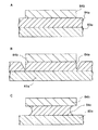
しかしながら図10のAに示すような基板83a上に成膜した配線形成用のCu膜84aの表面にマスクパターン84bを形成したものを、上記の過硫酸アンモニウムあるいはPAN系のエッチング剤に静止状態で浸漬し、エッチングを施すと、図10のBに示すようにマスクパターン84bの周辺のCu膜84aだけが異常に速くエッチングされてしまい、Cu膜84aの側面の中央部分のエッチング量が他の部分のエッチング量よりも増加し、図10のCに示すように得られる配線84cの線幅がマスクパターン84bの幅より狭くなってしまうというパターン細り現象が生じるという問題があった。
また、エッチング剤として酢酸−過酸化水素水系や過硫酸アンモニウムを用いた場合、エッチングレートの経時変化が激しいため、Cu膜の浸漬時間のコントロールが難しく、所望の線幅のCu配線を得るのが困難であった。なお、酢酸−過酸化水素水系を用いる場合は、上記のようなパターン細り現象は生じない。
【0006】
本発明は、上記事情に鑑みてなされたもので、低抵抗のCu膜を配線材料として用いる場合に、静止による浸漬法という簡易なケミカルエッチング法でCu膜をエッチングでき、しかもエッチングレートの経時変化が少なく、Cu膜の側面のエッチング量(サイドエッチング量)にバラツキが生じることに起因するパターン細り現象が生じるのを防止できるエッチング剤を提供することにある。
【0007】
【課題を解決するための手段】
本発明は、ペルオキソ一硫酸一水素カリウムを含有する水溶液からなることを特徴とする銅のエッチング剤を上記課題の解決手段とした。
かかる構成のエッチング剤によれば、静止による浸漬法という簡易なケミカルエッチング法でCu膜をエッチングでき、しかもエッチングレートの経時変化がなく、Cu膜のサイドエッチング量が均一であるので、所望の線幅の銅配線を容易に得ることができる。
上記銅のエッチング剤は、酢酸を含有していてもよい。かかるエッチング剤によれば、エッチングレートの経時変化がなく、Cu膜のサイドエッチング量を均一にできるうえ銅膜へのぬれ性も向上するので、微細な銅配線を形成する場合でも、寸法精度が優れた銅配線を形成できる。
【0008】
上記エッチング剤中のペルオキソ一硫酸一水素カリウムの濃度は、0.08乃至2.0mol/lであることが好ましく、より好ましくは0.1乃至1.0mol/lである。ペルオキソ一硫酸一水素カリウムの濃度が0.08mol/l未満であると、マスクパターンの周辺の銅膜だけが異常に速くエッチングされてしまい、得られる銅配線の線幅がマスクパターンの幅より狭くなってしまう。ペルオキソ一硫酸一水素カリウムの濃度が2.0mol/lを超えると、エッチングレートが速くなり過ぎて、得られる銅配線の線幅のコントロールが困難になってしまう。
【0009】
本発明のチタン膜と銅膜との積層膜のエッチング剤は、ペルオキソ一硫酸一水素カリウムとフッ酸とを含有する水溶液からなることを特徴とする。かかるエッチング剤によれば、積層膜を構成する銅膜のサイドエッチング量を均一とすることができるうえ、静止による浸漬法という簡易なケミカルエッチング法で上記積層膜を構成するチタン膜又はチタン合金膜と銅膜の両方を一括エッチングできる。
本発明のモリブデン膜と銅膜との積層膜のエッチング剤は、ペルオキソ一硫酸一水素カリウムとリン酸と硝酸とを含有する水溶液からなることを特徴とする。かかるエッチング剤によれば、積層膜を構成する銅膜のサイドエッチング量を均一とすることができるうえ、静止による浸漬法という簡易なケミカルエッチング法で上記積層膜を構成するモリブデン膜又はモリブデン合金膜と銅膜の両方を一括エッチングできる。
本発明のクロム膜と銅膜との積層膜のエッチング剤は、ペルオキソ一硫酸一水素カリウムと塩酸とを含有する水溶液からなることを特徴とする。かかるエッチング剤によれば、積層膜を構成する銅膜のサイドエッチング量を均一とすることができるうえ、静止による浸漬法という簡易なケミカルエッチング法で上記積層膜を構成するクロム膜又はクロム合金膜と銅膜の両方を一括エッチングできる。
【0010】
本発明のチタン膜と銅膜との積層膜のエッチング剤は、ペルオキソ硫酸塩とフッ酸と塩酸もしくは塩化物とを含有する水溶液からなることを特徴とするものであってもよい。かかるエッチング剤によれば、チタン膜又はチタン合金膜と銅膜との積層膜のエッチング剤として用いると、上記積層膜をエッチング残査なく一括エッチングでき、所望の線幅の積層配線を精度良く形成できるので、製造工程の簡略化ができるうえ歩留まりを向上できる。
ペルオキソ硫酸塩とフッ酸と塩酸もしくは塩化物とを含有する水溶液からなるエッチング剤中のCl濃度(Cl-イオン濃度)が大きくなると、エッチングレートを大きくでき、エッチング残査を少なくできるが、Cl濃度があまり大きくなりすぎると、エッチングレートが早くなりすぎて制御しにくくなるため、Cl濃度の上限としては、10%程度とすることが好ましい。
【0011】
本発明のチタン膜と銅膜の積層膜のエッチング剤は、ペルオキソ硫酸塩とフッ化物とを含有する水溶液からなるものであってもよい。かかるエッチング剤によれば、フッ化物に含まれるフッ素が水溶液中にF-イオンとして存在することとなるので、エッチング剤中にHFが含まれていなくても、チタン膜又はチタン合金膜と銅膜との積層膜をエッチング残査なく一括エッチングでき、所望の線幅の積層配線を精度良く形成できるので、製造工程の簡略化ができるうえ歩留まりを向上できる。このエッチング剤には、フッ酸が含まれていてもよい。
【0012】
上記ペルオキソ硫酸塩としては、KHSO5、NaHSO5、K2S2O8、Na2S2O8、(NH4)2S2O8のうちから選択されるいずれか一種以上のものが用いられる。
上記塩化物は、アルカリ金属の塩化物もしくは塩化アンモニウムが用いられ、具体例としてはKCl、NaCl、NH4Clなどが用いられる。
上記フッ化物としては、アルカリ金属のフッ化物もしくはフッ化アンモニウムが用いられ、具体例としてはKF、NaF、NH4Fなどが用いられる。
エッチング剤中の陽イオンを一種類にするために、好ましいペルオキソ硫酸塩と塩化物の組み合わせとしては、例えば、KHSO5とKCl、(NH4)2S2O8とNH4Clなどを挙げることができる。また、好ましいペルオキソ硫酸塩とフッ化物の組み合わせとしては、例えば、KHSO5とKF、(NH4)2S2O8とNH4Fなどを挙げることができる。
【0013】
本発明の電子機器用基板の製造方法は、基体上に銅膜を成膜し、該銅膜の表面に所定パターンのマスクを形成し、ペルオキソ一硫酸一水素カリウムを含有する上記のいずれかの構成の本発明の銅のエッチング剤を用いて上記銅膜をエッチングして上記所定パターンの銅配線を形成することを特徴とする。
かかる構成の電子機器用基板の製造方法によれば、静止による浸漬法という簡易なケミカルエッチング法でCu膜をエッチングでき、しかもエッチングレートの経時変化が少なく、Cu膜の側面のエッチング量(サイドエッチング量)が均一で、所望の線幅の銅配線を形成できるので、歩留まりが良好であり、製造工程が簡略で、製造効率を向上できる。従って、かかる構成の本発明の電子機器用基板の製造方法によれば、歩留まりの向上によるコストが低い電子機器用基板を得ることができる。
【0014】
本発明の電子機器用基板の製造方法は、基体上にチタン膜又はチタン合金膜と銅膜とを順次成膜した積層膜の表面に所定パターンのマスクを形成し、上記のいずれかの構成の本発明のチタン膜と銅膜とのエッチング剤を用いて上記チタン膜と銅膜との積層膜をエッチングして上記所定パターンの積層配線を形成することを特徴とする。
かかる構成の電子機器用基板の製造方法によれば、上記積層膜を構成する銅膜のサイドエッチング量を均一とすることができるうえ、静止による浸漬法という簡易なケミカルエッチング法で上記積層膜を構成するチタン膜又はチタン合金膜と銅膜の両方を一括エッチングできるので、歩留まりが良好であり、製造工程を短縮できる。従って、かかる構成の本発明の電子機器機器用基板の製造方法によれば、歩留まりの向上と製造効率の向上によるコストが低い電子機器用基板を得ることができる。
また、エッチング剤として、特に、ペルオキソ硫酸塩とフッ酸と塩酸もしくは塩化物とを含有する水溶液、あるいは、ペルオキソ硫酸塩とフッ化物とを含有する水溶液を用いる場合は、チタン膜又はチタン合金膜と銅膜との積層膜をエッチング残査なく一括エッチングでき、所望の線幅の積層配線を精度良く形成できるので、製造工程の簡略化ができるうえ歩留まりを向上できる。
【0015】
また、本発明の電子機器用基板の製造方法は、基体上に少なくとも第1の金属層と第1の絶縁層と半導体層と第2の金属層と第2の絶縁層とを有する電子機器用基板の製造方法であって、上記第1と第2の金属層のうち少なくとも一方を形成するに際して、チタン膜又はチタン合金膜と銅膜とを順次成膜した積層膜の表面に所定パターンのマスクを形成し、ペルオキソ硫酸塩とフッ酸と塩酸もしくは塩化物とを含有する水溶液、あるいはペルオキソ硫酸塩とフッ化物とを含有する水溶液からなるエッチング剤を用いて上記チタン膜又はチタン合金膜と銅膜との積層膜をエッチングして上記所定パターンの積層配線を形成することを特徴とする。
かかる構成の電子機器用基板の製造方法によれば、チタン膜又はチタン合金膜と銅膜との積層膜をエッチング残査なく一括エッチングでき、所望の線幅の積層配線を精度良く形成できるので、製造工程の簡略化ができるうえ歩留まりを向上できる。
上記電子機器用基板の製造方法において、上記半導体層をポリシリコンから形成するようにしてもよい。
【0016】
本発明の電子機器は、上記のいずれかの構成の電子機器用基板の製造方法により製造した基板を有することを特徴とする。
かかる構成の電子機器によれば、低抵抗配線として銅膜からなる銅配線あるいは銅膜を有する積層配線を用いた電子機器用基板が備えられているので、配線抵抗に起因する信号電圧低下や配線遅延が生じにくく、配線が長くなる大面積の表示や配線が細くなる高詳細な表示に最適な表示装置等を容易に実現できるという利点がある。
【0017】
【発明の実施の形態】
以下、図面により本発明について詳細に説明するが、本発明はこれらの実施形態例のみに限定されるものではない。
(第一実施形態)
図3は、本発明の電子機器用基板の製造方法を液晶表示装置に備えられる薄膜トランジスタ基板の製造方法(第一実施形態の薄膜トランジスタ基板の製造方法)に適用して製造された薄膜トランジスタ基板の例を示す部分断面図である。
符号aの部分は薄膜トランジスタ(TFT)部、bの部分はTFTマトリクス外側に位置するソース配線の端子部、cの部分はゲート配線の端子部を示している。なおこれら3つの部分は、この薄膜トランジスタ基板1が備えられる実際の液晶表示装置においては離れた箇所にあり、本来断面図を同時に示せるものではないが、図示の都合上、近接させて図示する。
【0018】
まず、薄膜トランジスタ部aの部分について説明する。
薄膜トランジスタ部aには、基板(基体)2上に膜厚50乃至100nm程度のTi膜又はTi合金膜3と膜厚100乃至200nm程度のCu膜4からなるゲート電極5が設けられている。その上にゲート絶縁膜7が設けられ、このゲート絶縁膜7上にアモルファスシリコン(a−Si)からなる半導体膜8が設けられ、さらにこの半導体膜8上にn+ 型a−Si層9が設けられ、その上にソース電極12およびドレイン電極14が設けられている。ソース電極12、ドレイン電極14は、膜厚50乃至100nm程度のTi 膜又はTi合金膜10と、膜厚100乃至200nm程度のCu膜1 1と、膜厚50乃至100nm程度のTi膜又はTi合金膜10から なるものである。
【0019】
また、ソース電極12やドレイン電極14の上方にこれらを覆うパッシベーション膜17(絶縁膜)が形成され、このパッシベーション膜17に、Cu膜11の上側に設けられたTi膜又はTi合金膜10に達するコンタクトホール18が形成されている。ここでのパッシベーション膜17の例としては、a(アモルファス)−SiNx:H、 a−SiNx、a−SiO2:H、SiO2等を挙げるこ とができる。
そして、コンタクトホール18の内壁面および底面に沿って画素電極となるITO層19が形成されている。このコンタクトホール18を通じてドレイン電極14とITO層19(画素電極)が電気的に接続されている。
【0020】
次に、ソース配線の端子部bに関しては、ゲート絶縁膜7上にTi膜又はTi合金膜10とCu膜11とTi膜又はTi合金膜10とからなる下部パッド層16aが形成され、その上にはパッシベーション膜17が形成され、Al膜又はAl合金膜11の上側に設けられたTi膜又はTi合金膜10に達するコンタクトホール20が形成されている。
そして、コンタクトホール20の内壁面および底面に沿ってITOからなる上部パッド層21が形成されている。このコンタクトホール20を通じて下部パッド層16aと上部パッド層21が電気的に接続されている。
【0021】
次に、ゲート配線の端子部cに関しては、基板2上にTi膜又はTi合金膜3と、Cu膜4からなる下部パッド層16bが形成され、その上にはゲート絶縁膜7が形成され、さらにこの上にパッシベーション膜17が形成され、Cu膜4に達するコンタクトホール22が形成されている。そして、コンタクトホール22の内壁面および底面に沿ってITOからなる上部パッド層23が形成されている。このコンタクトホール22を通じて下部パッド層16bと上部パッド層23が電気的に接続されている。
【0022】
次に、本発明の第一実施形態の薄膜トランジスタ基板の製造方法を図1乃至図2を用いて説明する。
図1乃至図2中、符号aの部分は薄膜トランジスタ(TFT)部、bの部分はTFTマトリクス外側に位置するソース配線の端子部、cの部分はゲート配線の端子部を示している。
まず、図1のAに示すように基板2上の全体にわたってスパッタ法を用いてTi膜又はTi合金膜3と、Cu膜4とを順に成膜して積層膜を形成する。
ついで、薄膜トランジスタ部aに関しては上記積層膜を構成するCu膜4上にフォトリソグラフィーにより所定パターンのマスクパターン27を形成した後、ペルオキソ一硫酸一水素カリウム(KHSO5)とフッ酸とを含有する水溶液か らなるエッチング剤を用いて上記積層膜に一括エッチングを施し、図1のBに示すようなTi膜又はTi合金膜3と銅膜4とからなるゲート電極5を形成する。ここで用いたエッチング剤中のペルオキソ一硫酸一水素カリウムの濃度は、0.08乃至2.0mol/lであることが好ましい。また、上記エッチング剤中のペルオキソ一硫酸一水素カリウムに対するフッ酸の濃度が0.05乃至2.0mol/lの範囲内になるように調整されていることが、上記積層膜を構成する各金属膜を一回のエッチングにより略同一エッチングレートでエッチングできる点で好ましい。また、上記エッチング剤は、酢酸を含有していることが積層膜へのぬれ性を向上できる点で好ましく、上記エッチング剤中のペルオキソ一硫酸一水素カリウムに対する酢酸の重量比が10乃至75wt%の範囲内になるように調整されていることが好ましい。
【0023】
一方、ゲート配線の端子部cに関しては上記積層膜を構成するCu膜4上にフォトリソグラフィーにより所定パターンのマスクパターン28を形成した後、先に用いたものと同様のエッチング剤を用いて上記積層膜に一括エッチングを施して、図1のBに示すようなTi膜又はTi合金膜3とCu膜4とからなる下部パッド層16bを形成する。
このようにすると、上記積層膜を構成するCu膜4のサイドエッチング量を均一とすることができるうえ、静止による浸漬法という簡易なケミカルエッチング法で上記Ti膜又はTi合金膜3とCu膜4の両方を同時にエッチングできる。
【0024】
次に、基板2の上面全体にCVD法を用いてゲート絶縁膜7を形成する。ついで、薄膜トランジスタ部aに関しては、半導体層8、n+ 型a−Si層9を形成した後、図1のCに示すようにTFTのチャネル部となるゲート電極5の上方部分を残すように半導体層8、n+型a−Si層9をエッチングする。
そして、薄膜トランジスタ部a及びソース配線の端子部bに関しては、図1のDに示すように、Ti膜又はTi合金膜10と、Cu膜11と、Ti膜又はTi合金膜10を順に成膜して積層膜を形成する。
【0025】
次に、薄膜トランジスタ部aに関しては、TFTのチャネル部となるゲート電極5の上方の上記積層膜のTi膜又はTi合金膜10上にフォトリソグラフィーにより所定パターンのマスクパターン37を形成した後、先に用いたものと同様のエッチング剤を用いて上記積層膜に一括エッチングを施して、図2のAに示すようなTi膜又はTi合金膜10とCu膜11とTi膜又はTi合金膜10とからなるソース電極12と、ドレイン電極14を形成する。
一方、ソース配線の端子部bに関しては上記積層膜のTi膜又はTi合金膜10上にフォトリソグラフィーにより所定パターンのマスクパターン38を行った後、先の用いたものと同様のエッチング剤を用いて上記積層膜に一括エッチングを施して、図2のAに示すようなTi膜又はTi合金膜10とCu膜11とTi膜又はTi合金膜10とからなる下部パッド層16aを形成する。
このようにすると、上記積層膜を構成するCu膜10のサイドエッチング量を均一とすることができるうえ、静止による浸漬法という簡易なケミカルエッチング法で上記Cu膜11とこれの上下のTi膜又はTi合金膜10を同時にエッチングできる。
その後、n+ 型a−Si層9を乾式法あるいは乾式法と湿式法との併用によりエッチングしてチャネル24を形成する。
【0026】
次に、薄膜トランジスタ部a、ソース配線の端子部b及びゲート配線の端子部cに関しては、Ti膜又はTi合金膜3,10上にパッシベーション膜17を形成する。
ついで、薄膜トランジスタ部aに関しては、図2のBに示すように、パッシベーション膜17を乾式法あるいは乾式法と湿式法との併用によりエッチングしてコンタクトホール18を形成した後、ITO層を全面に形成した後、パターニングすることにより、図3に示すように、コンタクトホール18の底面および内壁面、パッシベーション膜17の上面にかけてITO層19を形成する。
一方、ソース配線の端子部b、ゲート配線の端子部cについても同様でパッシベーション膜17を乾式法あるいは乾式法と湿式法との併用によりエッチングしてコンタクトホール20、22を形成(ただし、ゲート配線端子部cではパッシベーション膜17の他、さらにゲート絶縁膜7もエッチングしてコンタクトホール22を形成する)した後、ITO層を全面に形成した後、パターニングすることにより、図3に示すように、コンタクトホール20、22の底面および内壁面、パッシベーション膜17の上面にかけて上部パッド層21、23を形成する。このような手順で、図3に示すような薄膜トランジスタ基板1を製造することができる。
【0027】
第一実施形態の薄膜トランジスタ基板の製造方法においては、Ti膜又はTi合金膜3とCu膜4とを順に成膜した積層膜や、Cu膜11の上下にTi膜又はTi合金膜10を成膜した積層膜をエッチングして所定パターンのゲート電極5、ソース電極12、ドレイン電極14、下部パッド層16a,16bを形成する際に、エッチング剤としてペルオキソ一硫酸一水素カリウム(KHSO5)とフ ッ酸とを含有する水溶液からなるものを用いることにより、上記積層膜を構成する銅膜4、11のサイドエッチング量を均一とすることができるうえ、静止による浸漬法という簡易なケミカルエッチング法で上記積層膜を構成するTi膜又はTi合金膜3と銅膜4の両方を一括エッチングでき、また、上記積層膜が三層構造である場合は、Cu膜11とこれの上下のTi膜又はTi合金膜10を同時にエッチングできるので、歩留まりが良好であり、製造工程を短縮できる。従って、かかる構成の第一実施形態の薄膜トランジスタ基板の製造方法によれば、歩留まりの向上と製造効率の向上によるコストが低い薄膜トランジスタ基板を得ることができる。
【0028】
また、銅膜の下層にTi膜あるいはTi合金膜を設けた積層膜を用いるので、上記積層膜の下側の隣接膜から元素が拡散してきても上記Ti膜あるいはTi合金膜により積層膜への元素の拡散が阻害されるので、隣接膜からの元素の拡散に起因する配線抵抗の上昇を防止でき、例えば、上記基板2がガラス基板である場合に、上記ゲート電極5や下部パッド層16b形成用の銅膜4にガラス基板中のSiが入りこむことを防止できるので、上記銅膜4にSiが入り込むことに起因する配線抵抗の上昇を防止できる。
【0029】
また、銅膜11の上層にTi膜又はTi合金膜10を設けた積層膜を用いるので、空気中の水分や酸素に対する耐酸化性ならびにレジスト剥離液などに対する耐食性を向上できるので、ソース電極12、ドレイン電極14、下部パッド層16aが損傷を受けにくく、これら電極12,14や下部パッド層16aが下地から剥離するのを防止できるうえ断線不良の発生を防止できる。さらにまた、上記Ti膜又はTi合金膜10により銅膜11のCu原子が隣接膜に拡散するのを阻害できるので、銅膜11からのCu原子の拡散に起因する絶縁耐圧不良も防止できるうえ、半導体能動膜の特性の劣化を防止できる。また、積層膜の上側の隣接膜から元素が拡散してきてもTi膜又はTi合金膜10により電極12,14や下部パッド層16aへの元素の拡散が阻害されるので、隣接膜からの元素の拡散に起因する配線抵抗の上昇を防止できる。
【0030】
なお、本発明の技術範囲は上記実施の形態に限定されるものではなく、例えばCu膜、Ti膜又はTi合金膜、パッシベーション膜等の膜厚や、形状等について、本発明の趣旨を逸脱しない範囲において種々の変更を加えることが可能である。
また、上記の実施の形態においては、ゲート電極5、下部パッド層16bをTi膜又はTi合金膜3とCu膜4との積層膜を一括エッチングして形成する場合について説明したが、Cu膜の上下にTi膜又はTi合金膜を形成した三層構造の積層膜を一括エッチングして形成してもよい。
また、ソース電極12、ドレイン電極14、下部パッド層16aをCu膜11の上下にTi膜又はTi合金膜10を形成した三層構造の積層膜を一括エッチングして形成する場合について説明したが、Ti膜又はTi合金膜上にCu膜を成膜した二層構造の積層膜を一括エッチングして形成してもよい。
また、上記の実施の形態においては、上記積層膜のエッチング剤としてペルオキソ一硫酸一水素カリウムとフッ酸とを含有する水溶液からなるものを用いる場合について説明したが、ペルオキソ一硫酸一水素カリウムを含有する水溶液からなるエッチング剤を用いて上記積層膜をエッチングすると、Cu膜のみをエッチングする選択エッチングを施すことができ、その場合、Cu膜のエッチング前あるいはエッチング後にTi膜またはTi合金膜用のエッチング剤を用いてエッチング処理を施してもよい。
【0031】
また、Ti膜又Ti合金膜とCu膜とからなる積層膜のエッチング剤としては、上記のペルオキソ一硫酸一水素カリウムとフッ酸とを含有する水溶液に代えてペルオキソ硫酸塩とフッ酸と塩酸もしくは塩化物とを含有する水溶液あるいはペルオキソ硫酸塩とフッ化物とを含有する水溶液を用いてもよい。このようなエッチング剤を用いると、上記積層膜をエッチング残査なく一括エッチングでき、所望の線幅の積層配線を精度良く形成できるので、製造工程の簡略化ができるうえ歩留まりを向上できるという利点がある。
【0032】
(第二実施形態)
次に、本発明の第二実施形態の薄膜トランジスタ基板の製造方法を説明する。
第二実施形態の薄膜トランジスタ基板の製造方法が、上述の第一実施形態の薄膜トランジスタ基板の製造方法と異なるところは、ゲート電極5や下部パッド層16b形成用の積層膜としてMo膜又はMo合金膜とCu膜との積層膜を形成し、また、ソース電極12やドレイン電極14や下部パッド層16a形成用の積層膜としてCu膜の上下にMo膜又はMo合金膜を設けた積層膜を形成し、これら積層膜のエッチング剤としてペルオキソ一硫酸一水素カリウムとリン酸と硝酸とを含有する水溶液からなるものを用いる点である。
また、上記エッチング剤中のペルオキソ一硫酸一水素カリウムに対するリン酸の濃度が0.8乃至8mol/lの範囲内、また、ペルオキソ一硫酸一水素カリウムに対する硝酸の濃度が0.1乃至1.0mol/lの範囲内になるように調整されていることが、上記積層膜を構成する各金属膜を一回のエッチングにより略同一エッチングレートでエッチングできる点で好ましい。
【0033】
第二実施形態の薄膜トランジスタ基板の製造方法においては、Mo膜又はMo合金膜とCu膜とを順に成膜した積層膜や、Cu膜の上下にMo膜又はMo合金膜を成膜した積層膜をエッチングして所定パターンのゲート電極5、ソース電極12、ドレイン電極14、下部パッド層16a,16bを形成する際に、エッチング剤としてペルオキソ一硫酸一水素カリウムとリン酸と硝酸とを含有する水溶液からなるものを用いることにより、各積層膜を構成する銅膜のサイドエッチング量を均一とすることができるうえ、静止による浸漬法という簡易なケミカルエッチング法で上記積層膜を構成するMo膜又はMo合金膜と銅膜の両方を一括エッチングでき、また、上記積層膜が三層構造である場合は、Mo膜とこれの上下のMo膜又はMo合金膜を同時にエッチングできるので、歩留まりが良好であり、製造工程を短縮できる。
【0034】
(第三実施形態)
次に、本発明の第三実施形態の薄膜トランジスタ基板の製造方法を説明する。
第三実施形態の薄膜トランジスタ基板の製造方法が、上述の第一実施形態の薄膜トランジスタ基板の製造方法と異なるところは、ゲート電極5や下部パッド層16b形成用の積層膜としてCr膜又はCr合金膜とCu膜との積層膜を形成し、また、ソース電極12やドレイン電極14や下部パッド層16a形成用の積層膜としてCr膜又はCr合金膜とCu膜との積層膜を形成し、これら積層膜のエッチング剤としてペルオキソ一硫酸一水素カリウムと塩酸とを含有する水溶液からなるものを用いる点である。
また、上記エッチング剤中のペルオキソ一硫酸一水素カリウムに対する塩酸の濃度が4乃至11mol/lの範囲内になるように調整されていることが、上記積層膜を構成する各金属膜を一回のエッチングにより略同一エッチングレートでエッチングできる点で好ましい。このエッチング剤は、上記積層膜をエッチングする際に、上記積層膜が形成された基板2を該エッチング剤中に浸漬すると、マスクパターンによってマスクされていない領域において上記積層膜を構成するCu膜がペルオキソ一硫酸一水素カリウムにより効果的にエッチングでき、また、上記Cu膜のCuと上記塩酸が反応し、それによって気泡を生じながらCu膜の下層のCr又はCr合金膜が効果的にエッチングできる。
【0035】
第三実施形態の薄膜トランジスタ基板の製造方法においては、Cr膜又はCr合金膜とCu膜とを順に成膜した積層膜をエッチングして所定パターンのゲート電極5、ソース電極12、ドレイン電極14、下部パッド層16a,16bを形成する際に、エッチング剤としてペルオキソ一硫酸一水素カリウムと塩酸とを含有する水溶液からなるものを用いることにより、各積層膜を構成する銅膜のサイドエッチング量を均一とすることができるうえ、浸漬法という簡易なケミカルエッチング方法で上記積層膜を構成するCr膜又はCr合金膜と銅膜の両方を一括エッチングできるので、歩留まりが良好であり、製造工程を短縮できる。
なお、上記の第一乃至第三の実施形態では、Ti膜又はTi合金膜とCu膜との積層膜、Mo膜又はMo合金膜とCu膜との積層膜、Cr膜又はCr合金膜とCu膜との積層膜をエッチングする場合について説明したが、W膜又はW合金膜とCu膜の積層膜、Ta膜又はTaN等のTa合金膜とCu膜との積層膜、TiN膜とCu膜との積層膜、TiOx膜とCu膜との積層膜などをエッチングする 際に、エッチング剤としてペルオキソ一硫酸一水素カリウムを含有する水溶液を用いれば、Cu膜を選択的にエッチングでき、また、Mo膜とCu膜との積層膜をエッチングする際に、エッチング剤としてペルオキソ一硫酸一水素カリウムを含有する水溶液を用いれば、Mo膜のエッチングレートはCu膜のエッチングレートよりも小さいが、Mo膜とCu膜の両方をエッチングできる。
【0036】
(第四実施形態)
次に、本発明の第四実施形態の薄膜トランジスタ基板の製造方法を説明する。
図4は、本発明の第四実施形態の薄膜トランジスタ基板の製造方法により製造された薄膜トランジスタ基板の例を示す部分断面図である。この薄膜トランジスタ基板1aが、図3に示した薄膜トランジスタ基板1と異なるところは、ゲート電極5、下部パッド層16bがCu膜4から構成されており、ソース電極12、ドレイン電極14、下部パッド層16aもCu膜11から構成されている点である。
第四実施形態の薄膜トランジスタ基板の製造方法が、上述の第一実施形態の薄膜トランジスタ基板の製造方法と異なるところは、ゲート電極5、下部パッド層16b形成用の膜としてCu膜4を形成し、ソース電極12、ドレイン電極14、下部パッド層16a形成用の膜としてCu膜11を形成し、これらCu膜4、11のエッチング剤としてペルオキソ一硫酸一水素カリウムを含有する水溶液からなるものを用いる点である。
ここで用いるエッチング剤中のペルオキソ一硫酸一水素カリウムの濃度は、0.08乃至2.0mol/lであることが好ましい。また、上記エッチング剤は、酢酸を含有していることがCu膜へのぬれ性を向上できる点で好ましく、上記エッチング剤中のペルオキソ一硫酸一水素カリウムに対する酢酸の重量比が10乃至75wt%の範囲内になるように調整されていることが好ましい。
【0037】
第四実施形態の薄膜トランジスタ基板の製造方法においては、基板2上に成膜したCu膜4、11をエッチングして所定パターンのゲート電極5、ソース電極12、ドレイン電極14、下部パッド層16a,16bを形成する際に、エッチング剤としてペルオキソ一硫酸一水素カリウムを含有する水溶液からなるものを用いることにより、静止による浸漬法という簡易なケミカルエッチング法でCu膜4、11をエッチングでき、しかもエッチングレートの経時変化が少なく、Cu膜4、11の側面のサイドエッチング量が均一で、所望の線幅のゲート電極5、ソース電極12、ドレイン電極14、下部パッド層16a,16bを形成できるので、歩留まりが良好であり、製造工程が簡略で、製造効率を向上できる。従って、かかる構成の第四実施形態の薄膜トランジスタ基板の製造方法によれば、歩留まりの向上によるコストが低い薄膜トランジスタ基板を得ることができる。
【0038】
(第五実施形態)
図11は、本発明の第五実施形態の電子機器用基板の製造方法により得られた薄膜トランジスタ基板の部分断面図である。
符号aの部分は薄膜トランジスタ(TFT)部、bの部分はTFTマトリクス外側に位置するソース配線の端子部(パッド部)、dの部分は蓄積容量部(Cs部)を示している。なおこれら3つの部分は、この薄膜トランジスタ基板71が備えられる実際の液晶表示装置においては離れた箇所にあり、本来断面図を同時に示せるものではないが、図示の都合上、近接させて図示する。
【0039】
まず、薄膜トランジスタ部aの部分について説明する。
薄膜トランジスタ部aには、基板(基体)2上に絶縁層72を介してポリシリコンからなる半導体層73が形成され、この中央部上にゲート絶縁膜74が形成され、ゲート絶縁膜74上にゲート電極(第1の金属層)75が設けられている。ゲート電極75は、膜厚50乃至100nm程度のTi膜又はTi合金膜43と膜厚100乃至200nm程度のCu膜44から構成されている。なお、ゲート電極75は図示しないゲート配線と一体形成されている。そして、ゲート電極75上に層間絶縁膜(第1の絶縁層)76が設けられている。
また、半導体層73にはソース領域73aおよびドレイン領域73b が形成され、これらソース領域73a、ドレイン領域73bに挟まれた領域がチャネル部73cとなっている。また、これらソース領域73a、ドレイン領域73bをなす半導体層は、ゲート絶縁膜74端部の下方にまで侵入する形で形成されている。
【0040】
また、ソース領域73a上にソース配線(第2の金属層)77が形成され、ドレイン領域73b上にドレイン電極(第2の金属層)78が形成されている。これらソース配線77、ドレイン電極78は、膜厚50乃至100nm程度のTi膜又はTi合金膜79と膜厚100乃至200nm程度のCu膜80から構成されている。
そして、全面を覆うようにパッシベーション膜81が形成され、このパッシベーション膜81を貫通してドレイン電極78に達するコンタクトホール122が形成され、このコンタクトホール122を通じてドレイン電極78と接続されたITOからなる画素電極123が形成されている。
また、図示を省略するが、ゲート電極75と接続されたゲート配線端部のゲート端子部において、上記コンタクトホールと同様、ゲート配線を覆うパッシベーション膜81が開口し、ITOからなるパッドがゲート配線に接続してそれぞれ設けられている。
【0041】
次に、ソース配線77の端子部bに関しては、基板2上に形成した絶縁層72上に層間絶縁膜(第2の絶縁層)124が形成され、この層間絶縁膜124上にTi膜又はTi合金膜79とCu膜80とからなる下部パッド層77aが形成され、その上にはパッシベーション膜81が形成され、パッド層77aに達するコンタクトホール125が形成されている。
そして、コンタクトホール125の内壁面および底面に沿ってITOからなる上部パッド層125が形成されている。このコンタクトホール125を通じて下部パッド層77aと上部パッド層126が電気的に接続されている。
【0042】
次に、蓄積容量部dに関しては、基板2上に絶縁層72を介してTi膜又はTi合金膜43とCu膜44からなる容量線(第1の金属層)127が形成され、その上には層間絶縁膜(第2の絶縁層)128が形成され、さらにこの上にTi膜又はTi合金膜79とCu膜80からなる容量電極(第2の金属層)129が形成され、さらにこの上にパッシベーション膜81が形成され、容量電極129に達するコンタクトホール130が形成されている。そして、コンタクトホール130の内壁面および底面に沿ってITOからなる層131が形成されている。このコンタクトホール130を通じて層131と容量電極129が電気的に接続されている。
【0043】
図11に示したような電子機器用基板71に備えられるゲート電極(第1の金属層)75、容量線(第1の金属層)127は、スパッタ法、フォトリソグラフィー法により形成できるが、その際、Ti膜又はTi合金膜43とCu膜44とを順次成膜した積層膜の表面に所定パターンのマスクを形成し、ペルオキソ硫酸塩とフッ酸と塩酸もしくは塩化物とを含有する水溶液、あるいはペルオキソ硫酸塩とフッ化物とを含有する水溶液からなるエッチング剤を用いてTi膜又はTi合金膜43とCu膜44との積層膜をエッチングすることにより、上記所定パターンのゲート電極(第1の金属層)75、容量線(第1の金属層)127が得られる。
また、ソース配線(第2の金属層)77、ドレイン電極(第2の金属層)78、下部パッド層(第2の金属層)77a、容量電極(第2の金属層)129はスパッタ法、フォトリソグラフィー法により形成できるが、その際、Ti膜又はTi合金膜79とCu膜80とを順次成膜した積層膜の表面に所定パターンのマスクを形成し、ペルオキソ硫酸塩とフッ酸と塩酸もしくは塩化物とを含有する水溶液、あるいはペルオキソ硫酸塩とフッ化物とを含有する水溶液からなるエッチング剤を用いてTi膜又はTi合金膜79とCu膜80との積層膜をエッチングすることにより、上記所定パターンのソース配線(第2の金属層)77、ドレイン電極(第2の金属層)78、下部パッド層(第2の金属層)77a、容量電極(第2の金属層)129が得られる。
【0044】
第五実施形態の電子機器用基板の製造方法によれば、Ti膜又はTi合金膜43とCu膜44との積層膜や、Ti膜又はTi合金膜79とCu膜80との積層膜をエッチング残査なく一括エッチングでき、所望の線幅のゲート電極(第1の金属層)75、容量線(第1の金属層)127、ソース配線(第2の金属層)77、ドレイン電極(第2の金属層)78、下部パッド層(第2の金属層)77a、容量電極(第2の金属層)129を精度良く形成できるので、製造工程の簡略化ができるうえ歩留まりを向上できる。
【0045】
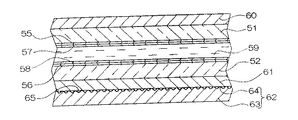
図5は、本発明の実施形態の薄膜トランジスタ基板の製造方法により製造された薄膜トランジスタ基板が備えられた反射型液晶表示装置の一例を示す概略図である。
この反射型液晶表示装置(電子機器)は、液晶層59を挟んで対向する上側および下側のガラス基板51、52の上側ガラス基板51の内面側に上側透明電極層55、上側配向膜57が上側ガラス基板51側から順に設けられ、下側ガラス基板52の内面側に下側透明電極層56、下側配向膜58が下側ガラス基板52側から順に設けられている。
液晶層59は、上側と下側の配向膜57、58間に配設されている。上側ガラス基板51の外面側には上側偏光板60が設けられ、下側ガラス基板52の外面側には下側偏光板61が設けられ、さらに下側偏光板61の外面側に反射板62が、反射膜64の凹凸面65を下側偏光板61側に向けて取り付けられている。反射板62は、例えば、表面にランダムな凹凸面が形成されたポリエステルフィルム63の凹凸面上にAlや銀などからなる金属反射膜64を蒸着等で成膜することにより形成されており、表面にランダムな凹凸面65を有しているものである。
【0046】
この反射型液晶表示装置においては、下側ガラス基板52が上記第一乃至第五のいずれかの薄膜トランジスタ基板の製造方法に適用して製造された薄膜トランジスタ基板の基板2、下側透明電極層56がITO層(画素電極)19に相当する。
この反射型液晶表示装置によれば、低抵抗配線として銅配線を用いた薄膜トランジスタ基板1aあるいは銅膜を有する積層配線を用いた薄膜トランジスタ基板1が備えられているので、配線抵抗に起因する信号電圧低下や配線遅延が生じにくく、配線が長くなる大面積の表示や配線が細くなる高詳細な表示に最適な表示装置を容易に実現できるという利点がある。
【0047】
【実施例】
以下、本発明を実施例により具体的に説明するが、本発明はこれらの実施例のみに限定されるものではない。
(実験例1)
エッチング剤として、オキソン(商品名:アルドリッチ社製、2KHSO5・ KHSO4・K2SO4が含まれる水溶液)水溶液と、過硫酸アンモニウム[(N H4)2S2O8]水溶液の2種類を用意し、各エッチング剤を用いてCu膜をエッチングしたときのCuエッチング速度のモル濃度依存性について以下のようにして調べた。
ガラス基板の表面に膜厚300nmのCu膜を形成した試験片を作製 し、この試験片をモル濃度を変更したエッチング剤を用いてエッチングしたときのエッチング速度を測定した。その結果を図6に示す。
図6に示した結果からオキソンからなる実施例のエッチング剤を用いた場合のエッチングレートは、過硫酸アンモニウム水溶液からなる比較例のエッチング剤を用いる場合とほぼ同様のエッチングレートが得られていることから、実施例のエッチング剤はCu膜のエッチング剤として使用できることがわかる。
【0048】
(実験例2)
上記実験例1で用いたものと同様のオキソン水溶液からなる実施例のエッチング剤と、過硫酸アンモニウム水溶液からなる比較例のエッチング剤を用意し、各エッチング剤を用いて上記試験片をエッチングしたときのCu膜の膜厚分布を調べた。ここでの試験片の表面には、所定のパターン(目標配線幅200μm)を有するマスクパターンを配置した。結果を図7に示す。図7中、横軸が基板上の膜厚測定位置(μm)、縦軸がデプスプロファイル(膜厚)である。図7中、鎖線は比較例のエッチング剤を用いた場合の結果、実線は実施例のエッチング剤を用いた場合の結果である。
図7に示した結果から比較例のエッチング剤を用いる場合、Cu配線以外のところにCu膜が残っており、マスクパターン周辺だけが異常に速くエッチングされ、エッチングが不完全であり、また、得られるCu配線の幅も160μm程度であり、目標配線幅より40μm程度も小さく、パターン細り現象が生じていることがわかる。これに対して実施例のエッチング剤を用いる場合、マスクパターン周辺が異常に速くエッチングされる現象がなく、Cu配線以外の部分にはCu膜がなく、また、得られるCu配線の幅もほぼ200μmであり、寸法精度が優れたCu配線が形成されていることがわかる。
【0049】
(実験例3)
0.05mol/1のオキソン水溶液(KHSO5は0.1mol/1)か らなる実施例のエッチング剤と、0.05mol/1過硫酸アンモニウム水溶液からなる比較例のエッチング剤を用意し、各エッチング剤を用いて上記試験片をエッチングしたときのエッチングレートの経時変化を調べた。結果を図8に示す。 図8に示した結果から比較例のエッチング剤を用いる場合、初日から4日あたりまでのエッチングレートの経時変化が激しく、4日以上では経時変化が小さくなっていることがわかる。これに対して実施例のエッチング剤は、初日から17日あたりまでエッチングレートが変化せず、17日以上でも経時変化が小さいことがわかる。
従って実験例1乃至3から、Cu膜のエッチング剤として、オキソンのようにペルオキソ一硫酸一水素カリウム(KHSO5)を含むようなエッチング剤を用 いると、エッチングレートの経時変化がなく、Cu膜のサイドエッチング量を均一とすることができるので、所望の線幅の銅配線を容易に得ることができることがわかる。
【0050】
(実験例4)
厚さ50nmの各種の下地膜(Cr膜、Ti膜、Mo膜、W膜、TiNi膜)上に100nmのCu膜を形成した積層膜を形成したガラス基板を0.05Mオキソン水溶液からなる実施例のエッチング剤(KHSO5は0.1mol/1)に0.5時間浸漬したときの下地金属膜のエッチ ング選択性について調べた。その結果を表1に示す。
【0051】
【表1】

表1に示した結果からエッチング剤として0.05Mオキソン水溶液を用いる場合、Cr膜とCu膜との積層膜のCr膜、Ti膜とCu膜との積層膜のTi膜、W膜とCu膜との積層膜のW膜、TiN膜とCu膜との積層膜のTiN膜のいずれもエッチングされていないことがわかる。また、Mo膜とCu膜との積層膜の場合、Mo膜が8nm/分でエッチングされることが分かった。なお、300nmのCu膜を用いた時、いずれの積層膜もCu膜は、160nm/分でエッチングされた。
【0053】
(実験例5)
ガラス基板の表面に膜厚300nmのCu単層膜をスパッタ法、フォトリソグラフィー法により形成した試験片を作製し、この試験片を、HFと過硫酸アンモニウム[(NH4)2S2O8]とHClを含む水溶液(HFの濃度は0.2%、(NH4)2S2O8の濃度は2%)からなるエッチング剤を用いてエッチングする際に、エッチング剤中のHCl濃度を0%〜0.5%の範囲で変更したときのCu膜のエッチング深さのHCl濃度依存性について調べた。その結果を図12に示す。
図12に示した結果から、Cu単層膜を形成した試験片を、HFと過硫酸アンモニウム[(NH4)2S2O8]とHClを含む水溶液からなるエッチング剤を用いてエッチングした場合、HCl濃度が0.5%の場合のエッチングレートは300nm/分程度であり、HCl濃度が0%の場合のエッチングレートは130nm/分程度であり、エッチング剤中のHCl濃度(Cl-イオンの濃度)が大きくなるに従ってエッチング深さが大きくなっていることがわかる。
なお、HClに代えてKClまたはNH4Clが含まれるエッチング剤を用いた場合もCl-イオンの濃度が大きくなるに従ってエッチング深さが大きくなった。 以上のことからペルオキソ硫酸塩とフッ酸と塩酸もしくは塩化物とを含有する水溶液からなるエッチング剤中のCl濃度が大きくなると、Cu単層膜のエッチングレートを大きくできることがわかる。
【0054】
(実験例6)
ガラス基板の表面に膜厚50nmのTi単層膜をスパッタ法、フォトリソグラフィー法により形成した試験片を作製し、この試験片を、HFと過硫酸アンモニウム[(NH4)2S2O8]とHClを含む水溶液(HFの濃度は0.2%、(NH4)2S2O8の濃度は2%)からなるエッチング剤を用いてエッチングする際に、エッチング剤中のHCl濃度を0%〜0.5%の範囲で変更したときのTi単層膜のエッチングオフ時間(エッチングが終了するまでの時間)のHCl濃度依存性について調べた。その結果を図13に示す。
図13に示した結果から、Ti単層膜を形成した試験片を、HFと過硫酸アンモニウム[(NH4)2S2O8]とHClを含む水溶液からなるエッチング剤を用いてエッチングした場合、HCl濃度を変更してもエッチングオフ時間はほとんど変化していないことから、エッチングレートはほぼ一定であることがわかる。それは、Ti単層膜からなる配線をスパッタ法、フォトリソグラフィー法により形成する場合、配線の表面に2〜5nm程度のTiOx膜が生成してしまい、このTiOx膜はエッチングし難いため、エッチングレートが低くなってしまうからである。
【0055】
(実験例7)
ガラス基板の表面に膜厚50nmのTi膜(下地層)と膜厚100nmのCu膜とからなる積層膜をスパッタ法、フォトリソグラフィー法により形成した試験片を作製し、この試験片を、HFと過硫酸アンモニウム[(NH4)2S2O8]とHClを含む水溶液(HFの濃度は0.2%、(NH4)2S2O8の濃度は2%)からなるエッチング剤を用いてエッチングする際に、エッチング剤中のHCl濃度を0%〜0.5%の範囲で変更したときのTi膜とCu膜の積層膜のエッチングオフ時間(エッチングが終了するまでの時間)のHCl濃度依存性について調べた。その結果を図14に示す。なお、ここで形成した積層膜のTi膜とこれの上層のCu膜は、空気中に曝露されることなくスパッタ法により連続成膜したものである。
図14に示した結果からTi膜とCu膜からなる積層膜を形成した試験片をHFと過硫酸アンモニウム[(NH4)2S2O8]とHClとを含む水溶液からなるエッチング剤を用いてエッチングする場合、エッチング剤中のHCl濃度(Cl-イオンの濃度)が大きくなるに従ってエッチングオフ時間が短くなっており、エッチングレートが高いことがわかる。
【0056】
図12乃至図14に示した結果からエッチング剤中のHCl濃度が0.1%の場合、Cu単層膜を100nmの深さまでエッチングするのに約24秒程度かかっており、また、厚さ50nmのTi単層膜を形成した試験片のエッチングオフ時間は約90秒かかっているのに対して、厚さ50nmのTi膜と厚さ100nmのCu膜を連続成膜して積層膜を形成した試験片のエッチングオフ時間は約30秒であることから、HFと過硫酸アンモニウム[(NH4)2S2O8]とHClを含む水溶液は、Ti単層膜をエッチングするときよりもTi膜とCu膜の積層膜をエッチングするときのエッチングオフ時間を大幅に短くでき、Cu単層膜をエッチングする場合に近いエッチングレートでエッチングできることがわかる。それは、Ti膜とCu膜を連続成膜する場合は、Cu膜形成前に空気中に曝露しせず、Ti膜の表面にTiOx膜が生成されないため、短時間でエッチングできるからである。
従って、HFと過硫酸アンモニウムとHClを含む水溶液は、Ti膜とCu膜の積層膜のエッチング剤として用いると、上記積層膜をエッチング残査なく一括エッチングでき、所望の線幅の積層配線を精度良く形成できるので、製造工程の簡略化ができるうえ歩留まりを向上できることがわかる。
【0057】
(実験例8)
ガラス基板の表面に膜厚50nmのTi膜(下地層)と膜厚100nmのCu膜とからなる積層膜をスパッタ法、フォトリソグラフィー法により形成した試験片を作製し、この試験片を、KF又はNH4Fと、3%のオキソン(商品名:アルドリッチ社製、2KHSO5・ KHSO4・K2SO4が含まれる水溶液)とを含む水溶液からなるエッチング剤を用いてエッチングする際に、エッチング剤中のKF又はNH4F濃度を0%〜0.5%の範囲で変更したときのTi膜とCu膜の積層膜のエッチングオフ時間(エッチングが終了するまでの時間)のKFまたはNH4F濃度依存性について調べた。その結果を図15に示す。なお、ここで形成した積層膜のTi膜とこれの上層のCu膜は、空気中に曝露されることなくスパッタ法により連続成膜したものである。
図15に示した結果からTi膜とCu膜からなる積層膜を形成した試験片はKF又はNH4Fと3%のオキソンとを含む水溶液からなるエッチング剤を用いてエッチングすることができ、また、このエッチング剤中のKFまたはNH4F濃度(F-イオンの濃度)が大きくなるに従ってエッチングオフ時間が短くなっており、エッチング残査がないうえエッチングレートが高いことがわかる。また、エッチング剤中にHFが含まれていなくても、エッチング剤にペルオキソ硫酸塩以外にF-イオンが含まれていれば、Ti膜とCu膜の積層膜を一括エッチングできることがわかる。
【0058】
(実験例9)
ガラス基板の表面に膜厚300nmのCu単層膜をスパッタ法、フォトリソグラフィー法により形成した試験片を作製し、この試験片を、KF又はHFと、3%のオキソン(商品名:アルドリッチ社製、2KHSO5・ KHSO4・K2SO4が含まれる水溶液)からなるエッチング剤を用いてエッチングする際に、エッチング剤中のKFの濃度を0.1%〜0.5%を変更したときと、KFに代えて0.2%のHFを用いたときのエッチング時間とCu単層膜のエッチング深さとの関係について調べた。その結果を図16に示す。
図16に示した結果から、Cu単層膜を形成した試験片をエッチングする場合、エッチング剤中にKFが含まれている場合の方が、HFが含まれている場合よりもエッチングレートが高いことがわかる。また、エッチング剤中のKF濃度が0.5%の場合の方が、KF濃度が0.1%の場合よりもエッチングレートが高くなっていることから、KF濃度(F-イオンの濃度)が大きい方がエッチング効率が良好であることがわかる。
なお、エッチング剤中にHFが含まれている場合の方は、KFが含まれている場合に比べてエッチングレートは低いが、制御はし易いことがわかる。
【0059】
【発明の効果】
以上詳細に説明した通り本発明の銅のエッチング剤は、ペルオキソ一硫酸一水素カリウムを含有する水溶液からなるものであるので、静止による浸漬法という簡易なケミカルエッチング法でCu膜をエッチングでき、しかもエッチングレートの経時変化がなく、Cu膜のサイドエッチング量が均一であるので、所望の線幅の銅配線を容易に得ることができる。
【図面の簡単な説明】
【図1】 本発明の電子機器用基板の製造方法の第一実施形態の薄膜トランジスタ基板の製造方法を工程順に示した概略図である。
【図2】 本発明の電子機器用基板の製造方法の第一実施形態の薄膜トランジスタ基板の製造方法を工程順に示した概略図である。
【図3】 本発明の第一実施形態の電子機器用基板の製造方法により得られた薄膜トランジスタ基板の部分断面図である。
【図4】 本発明の第四実施形態の薄膜トランジスタ基板の製造方法により製造された薄膜トランジスタ基板の部分断面図である。
【図5】 本発明の第一乃至第五のいずれかの実施形態の薄膜トランジスタ基板により製造された薄膜トランジスタ基板を有する反射型液晶表示装置の一例を示す概略図である。
【図6】 実施例と比較例のエッチング剤を用いてCu膜をエッチングしたときのCuエッチング速度のモル濃度依存性を示す図である。
【図7】 実施例と比較例のエッチング剤を用いてCu膜をエッチングしたときのCu膜の膜厚分布を示す図である。
【図8】 実施例と比較例のエッチング剤を用いてCu膜をエッチングしたときのエッチングレートの経時変化を示す図である。
【図9】 一般的な薄膜トランジスタ型液晶表示装置の薄膜トランジスタ部分を示す概略図である。
【図10】 従来の電子機器用基板の製造方法を工程順に示した概略図である。
【図11】 本発明の第五実施形態の電子機器用基板の製造方法により得られた薄膜トランジスタ基板の部分断面図である。
【図12】 エッチング剤中のHCl濃度を0%〜0.5%の範囲で変更したときのCu単層膜のエッチング深さのHCl濃度依存性を示すグラフである。
【図13】 エッチング剤中のHCl濃度を0%〜0.5%の範囲で変更したときのTi単層膜のエッチングオフ時間のHCl濃度依存性を示すグラフである。
【図14】 エッチング剤中のHCl濃度を0%〜0.5%の範囲で変更したときのTi膜とCu膜の積層膜のエッチングオフ時間のHCl濃度依存性を示すグラフである。
【図15】 エッチング剤中のKF又はNH4F濃度を0%〜0.5%の範囲で変更したときのTi膜とCu膜の積層膜のエッチングオフ時間のKFまたはNH4F濃度依存性を示すグラフである。
【図16】 エッチング剤中のKFの濃度を0.1%〜0.5%を変更したときと、KFに代えて0.2%のHFを用いたときのエッチング時間とCu単層膜のエッチング深さとの関係を示すグラフである。
【符号の説明】
1、1a、71・・・薄膜トランジスタ基板(電子機器用基板)、2・・・基板(基体)、3、43、79・・・Ti膜又はTi合金膜、4、44、80・・・Cu膜、5・・・ゲート電極(積層配線)、10・・・Ti膜又はTi合金膜、11・・・Cu膜、12・・・ソース電極 (積層配線)、 14・・・ドレイン電極(積層配線)、16a、16b・・・下部パッド層(積層配線)、27,28・・・マスクパターン(マスク)、37,38・・・マスクパターン(マスク)、52・・・ガラス基板、73・・・半導体層、75・・・ゲート電極(第1の金属層)、76・・・層間絶縁膜(第1の絶縁層)、77・・・ソース配線(第2の金属層)、77a・・・下部パッド層(第2の金属層)、78・・・ドレイン電極(第2の金属層)、124・・・層間絶縁膜(第2の絶縁層)、127・・・容量線(第1の金属層)、129・・・容量電極(第2の金属層)、128・・・層間絶縁膜(第2の絶縁層)。[0001]
BACKGROUND OF THE INVENTION
The present invention relates to an etching agent for producing a wiring using low-resistance copper, a method for manufacturing a substrate for electronic equipment using the same, and an electronic equipment.
[0002]
[Prior art]
A thin film transistor type liquid crystal display device can be given as one type of electronic equipment.
FIG. 9 is a schematic view showing a thin film transistor portion of a general thin film transistor type liquid crystal display device.
In this
[0003]
Further, the left part of FIG. 9 shows a cross-sectional structure of the gate
[0004]
In recent years, with the speeding up of liquid crystal display devices and the like, the problem of signal transmission delay due to the resistance of electrodes and wiring such as gate electrode, gate wiring, source electrode, drain electrode, source wiring, drain wiring, etc. has become obvious. In order to solve such a problem, use of copper having a lower resistance than Al or Al alloy as a wiring material has been studied. In addition, the material which comprises electrodes, such as a gate electrode, is also called wiring material here.
In the case of copper wiring, a Cu film is formed by a normal sputtering method in the same way as when wiring is made of Al or Al alloy, and then a mask pattern of a predetermined pattern is formed on the surface of this Cu film by photolithography, and then an etching agent It can be formed by etching the Cu film using and removing the Cu film at a place other than the wiring formation position.
[0005]
[Problems to be solved by the invention]
By the way, as a Cu etching agent, a PAN (phosphoric acid-acetic acid-nitric acid) etching agent, ammonium persulfate, and an acetic acid-hydrogen peroxide aqueous etching agent are known, and are often used as etching agents for fine processing. Yes.
However, the
In addition, when an acetic acid-hydrogen peroxide solution system or ammonium persulfate is used as an etching agent, it is difficult to control the immersion time of the Cu film, and it is difficult to obtain a Cu wiring having a desired line width because the etching rate changes with time. Met. In addition, when the acetic acid-hydrogen peroxide system is used, the pattern thinning phenomenon as described above does not occur.
[0006]
The present invention has been made in view of the above circumstances, and when a low resistance Cu film is used as a wiring material, the Cu film can be etched by a simple chemical etching method called a dipping method by staticity, and the etching rate changes over time. It is an object of the present invention to provide an etching agent that can prevent pattern thinning due to variations in the etching amount (side etching amount) on the side surface of the Cu film.
[0007]
[Means for Solving the Problems]
The present invention uses a copper etching agent characterized by comprising an aqueous solution containing potassium monohydrogen peroxomonosulfate as a means for solving the above problems.
According to the etching agent having such a configuration, the Cu film can be etched by a simple chemical etching method called a static immersion method, and the etching rate does not change with time, and the side etching amount of the Cu film is uniform. A copper wiring having a width can be easily obtained.
The copper etching agent may contain acetic acid. According to such an etchant, the etching rate does not change with time, the amount of side etching of the Cu film can be made uniform, and the wettability to the copper film is improved, so that the dimensional accuracy can be improved even when a fine copper wiring is formed. Excellent copper wiring can be formed.
[0008]
The concentration of potassium hydrogen peroxomonosulfate in the etching agent is preferably 0.08 to 2.0 mol / l, more preferably 0.1 to 1.0 mol / l. If the concentration of potassium peroxomonosulfate is less than 0.08 mol / l, only the copper film around the mask pattern is etched abnormally fast, and the resulting copper wiring is narrower than the mask pattern. turn into. When the concentration of potassium peroxomonosulfate exceeds 2.0 mol / l, the etching rate becomes too fast, and it becomes difficult to control the line width of the obtained copper wiring.
[0009]
The etching agent for the laminated film of the titanium film and the copper film according to the present invention is characterized by comprising an aqueous solution containing potassium peroxomonosulfate monohydrogen sulfate and hydrofluoric acid. According to such an etching agent, the side etching amount of the copper film constituting the laminated film can be made uniform, and the titanium film or the titanium alloy film constituting the laminated film by a simple chemical etching method called a dipping method by stationary And both copper films can be etched at once.
The etching agent for the laminated film of the molybdenum film and the copper film according to the present invention is characterized by comprising an aqueous solution containing potassium peroxomonosulfate monohydrogen sulfate, phosphoric acid and nitric acid. According to such an etching agent, the side etching amount of the copper film constituting the laminated film can be made uniform, and the molybdenum film or the molybdenum alloy film constituting the laminated film by a simple chemical etching method called a dipping method by static And both copper films can be etched at once.
The etching agent for the laminated film of the chromium film and the copper film of the present invention is characterized by comprising an aqueous solution containing potassium peroxomonosulfate and hydrochloric acid. According to such an etching agent, the amount of side etching of the copper film constituting the laminated film can be made uniform, and the chromium film or the chromium alloy film constituting the laminated film by a simple chemical etching method called a static immersion method. And both copper films can be etched at once.
[0010]
The etching agent for the laminated film of the titanium film and the copper film of the present invention may be characterized by comprising an aqueous solution containing peroxosulfate, hydrofluoric acid, hydrochloric acid or chloride. According to such an etching agent, when used as an etching agent for a laminated film of a titanium film or a titanium alloy film and a copper film, the laminated film can be collectively etched without etching residue, and a laminated wiring having a desired line width can be accurately formed. Therefore, the manufacturing process can be simplified and the yield can be improved.
The concentration of Cl in an etching agent comprising an aqueous solution containing peroxosulfate, hydrofluoric acid and hydrochloric acid or chloride (Cl - If the ion concentration is increased, the etching rate can be increased and the etching residue can be reduced. However, if the Cl concentration is too large, the etching rate becomes too fast and difficult to control. About 10% is preferable.
[0011]
The etching agent for the laminated film of the titanium film and the copper film of the present invention may be an aqueous solution containing peroxosulfate and fluoride. According to such an etching agent, fluorine contained in the fluoride is F in the aqueous solution. - Since it exists as ions, even if the etching agent does not contain HF, the laminated film of the titanium film or titanium alloy film and the copper film can be collectively etched without any etching residue, and a laminated film having a desired line width. Since the wiring can be formed with high accuracy, the manufacturing process can be simplified and the yield can be improved. This etchant may contain hydrofluoric acid.
[0012]
Examples of the peroxosulfate include KHSO. Five , NaHSO Five , K 2 S 2 O 8 , Na 2 S 2 O 8 , (NH Four ) 2 S 2 O 8 Any one or more selected from the above are used.
As the chloride, alkali metal chloride or ammonium chloride is used, and specific examples include KCl, NaCl, NH. Four Cl or the like is used.
As the fluoride, alkali metal fluoride or ammonium fluoride is used, and specific examples include KF, NaF, NH. Four F or the like is used.
In order to make one kind of cation in the etching agent, a preferable combination of peroxosulfate and chloride includes, for example, KHSO. Five And KCl, (NH Four ) 2 S 2 O 8 And NH Four And Cl. Moreover, as a preferable combination of peroxosulfate and fluoride, for example, KHSO Five And KF, (NH Four ) 2 S 2 O 8 And NH Four F etc. can be mentioned.
[0013]
The method for manufacturing a substrate for electronic equipment according to the present invention includes forming a copper film on a substrate, forming a mask having a predetermined pattern on the surface of the copper film, and containing any one of the above-mentioned potassium peroxomonosulfate. The copper film is etched using the copper etching agent of the present invention having the configuration to form the copper wiring of the predetermined pattern.
According to the method for manufacturing a substrate for an electronic device having such a configuration, the Cu film can be etched by a simple chemical etching method called a stationary immersion method, and the etching rate changes little with time, and the etching amount (side etching) on the side surface of the Cu film is reduced. Quantity) is uniform, and a copper wiring having a desired line width can be formed. Therefore, the yield is good, the manufacturing process is simplified, and the manufacturing efficiency can be improved. Therefore, according to the method for manufacturing an electronic device substrate of the present invention having such a configuration, it is possible to obtain an electronic device substrate having a low cost due to an improvement in yield.
[0014]
According to the method for manufacturing an electronic device substrate of the present invention, a mask having a predetermined pattern is formed on the surface of a laminated film in which a titanium film or a titanium alloy film and a copper film are sequentially formed on a substrate. The laminated wiring of the predetermined pattern is formed by etching the laminated film of the titanium film and the copper film using the etching agent for the titanium film and the copper film of the present invention.
According to the method for manufacturing an electronic device substrate having such a configuration, the amount of side etching of the copper film constituting the laminated film can be made uniform, and the laminated film can be formed by a simple chemical etching method called a static immersion method. Since both the titanium film or titanium alloy film and the copper film to be formed can be collectively etched, the yield is good and the manufacturing process can be shortened. Therefore, according to the method for manufacturing a substrate for electronic equipment of the present invention having such a configuration, it is possible to obtain a substrate for electronic equipment having a low cost due to an improvement in yield and an improvement in manufacturing efficiency.
In addition, when an aqueous solution containing peroxosulfate, hydrofluoric acid and hydrochloric acid or chloride, or an aqueous solution containing peroxosulfate and fluoride is used as an etchant, a titanium film or a titanium alloy film, Since the laminated film with the copper film can be collectively etched without etching residue, and a laminated wiring having a desired line width can be formed with high accuracy, the manufacturing process can be simplified and the yield can be improved.
[0015]
The electronic device substrate manufacturing method of the present invention is for an electronic device having at least a first metal layer, a first insulating layer, a semiconductor layer, a second metal layer, and a second insulating layer on a substrate. A method of manufacturing a substrate, wherein when forming at least one of the first and second metal layers, a mask having a predetermined pattern is formed on a surface of a laminated film in which a titanium film or a titanium alloy film and a copper film are sequentially formed. The titanium film or the titanium alloy film and the copper film are formed using an etchant comprising an aqueous solution containing peroxosulfate, hydrofluoric acid, hydrochloric acid or chloride, or an aqueous solution containing peroxosulfate and fluoride. The laminated film having the predetermined pattern is formed by etching the laminated film.
According to the method for manufacturing an electronic device substrate having such a configuration, a laminated film of a titanium film or a titanium alloy film and a copper film can be collectively etched without etching residue, and a laminated wiring having a desired line width can be accurately formed. The manufacturing process can be simplified and the yield can be improved.
In the electronic device substrate manufacturing method, the semiconductor layer may be formed of polysilicon.
[0016]
The electronic device of the present invention includes a substrate manufactured by the method for manufacturing an electronic device substrate having any one of the above-described configurations.
According to the electronic device having such a configuration, since the substrate for an electronic device using the copper wiring made of a copper film or the laminated wiring having the copper film is provided as the low resistance wiring, the signal voltage drop or wiring caused by the wiring resistance is provided. There is an advantage that it is possible to easily realize a display device and the like that are less likely to cause delay and that are optimal for a large-area display in which the wiring is long and a high-detail display in which the wiring is thin.
[0017]
DETAILED DESCRIPTION OF THE INVENTION
Hereinafter, the present invention will be described in detail with reference to the drawings. However, the present invention is not limited only to these embodiment examples.
(First embodiment)
FIG. 3 shows an example of a thin film transistor substrate manufactured by applying the method for manufacturing an electronic device substrate of the present invention to a method for manufacturing a thin film transistor substrate provided in a liquid crystal display device (a method for manufacturing a thin film transistor substrate of the first embodiment). It is a fragmentary sectional view shown.
Reference numeral a represents a thin film transistor (TFT) portion, b represents a source wiring terminal located outside the TFT matrix, and c represents a gate wiring terminal. Note that these three portions are located apart from each other in the actual liquid crystal display device provided with the thin film transistor substrate 1, and are not shown in a sectional view at the same time, but are shown close to each other for the sake of illustration.
[0018]
First, the thin film transistor portion a will be described.
The thin film transistor portion a is provided with a
[0019]
In addition, a passivation film 17 (insulating film) is formed over the
An
[0020]
Next, with respect to the terminal portion b of the source wiring, a
An
[0021]
Next, for the terminal portion c of the gate wiring, the
[0022]
Next, a method for manufacturing the thin film transistor substrate according to the first embodiment of the present invention will be described with reference to FIGS.
In FIG. 1 and FIG. 2, a part a represents a thin film transistor (TFT) part, a part b represents a terminal part of a source wiring located outside the TFT matrix, and a part c represents a terminal part of a gate wiring.
First, as shown in FIG. 1A, a Ti film or
Next, for the thin film transistor portion a, a
[0023]
On the other hand, with respect to the terminal part c of the gate wiring, a
In this way, the side etching amount of the
[0024]
Next, the
For the thin film transistor portion a and the terminal portion b of the source wiring, as shown in FIG. 1D, a Ti film or
[0025]
Next, with respect to the thin film transistor portion a, after a
On the other hand, with respect to the terminal portion b of the source wiring, a
In this way, the amount of side etching of the
Then n + The channel a is formed by etching the
[0026]
Next, a
Next, with respect to the thin film transistor portion a, as shown in FIG. 2B, the
On the other hand, the same applies to the terminal portion b of the source wiring and the terminal portion c of the gate wiring, and the
[0027]
In the method of manufacturing the thin film transistor substrate according to the first embodiment, a Ti film or a
[0028]
In addition, since a laminated film in which a Ti film or a Ti alloy film is provided under the copper film is used, even if an element diffuses from an adjacent film below the laminated film, the Ti film or Ti alloy film can be used to form the laminated film. Since element diffusion is hindered, an increase in wiring resistance due to element diffusion from the adjacent film can be prevented. For example, when the
[0029]
Further, since a laminated film in which a Ti film or a
[0030]
The technical scope of the present invention is not limited to the above-described embodiment, and the thickness, shape, and the like of a Cu film, a Ti film or a Ti alloy film, a passivation film, and the like do not depart from the spirit of the present invention. Various changes can be made in the range.
In the above-described embodiment, the case where the
In addition, the case where the
Further, in the above-described embodiment, the case of using an aqueous solution containing potassium peroxomonosulfate and hydrofluoric acid as the etching agent for the laminated film has been described. However, it contains potassium peroxomonohydrogensulfate. When the laminated film is etched using an etchant made of an aqueous solution, selective etching for etching only the Cu film can be performed. In this case, etching for the Ti film or Ti alloy film is performed before or after etching the Cu film. Etching treatment may be performed using an agent.
[0031]
Further, as an etching agent for a laminated film composed of a Ti film or a Ti alloy film and a Cu film, peroxosulfate, hydrofluoric acid, hydrochloric acid or An aqueous solution containing chloride or an aqueous solution containing peroxosulfate and fluoride may be used. When such an etchant is used, the laminated film can be collectively etched without any etching residue, and a laminated wiring having a desired line width can be formed with high accuracy, so that the manufacturing process can be simplified and the yield can be improved. is there.
[0032]
(Second embodiment)
Next, a manufacturing method of the thin film transistor substrate according to the second embodiment of the present invention will be described.
The manufacturing method of the thin film transistor substrate of the second embodiment differs from the manufacturing method of the thin film transistor substrate of the first embodiment described above in that a Mo film or a Mo alloy film is used as a laminated film for forming the
Further, the concentration of phosphoric acid relative to potassium peroxomonosulfate in the etching agent is in the range of 0.8 to 8 mol / l, and the concentration of nitric acid relative to potassium monohydrogen persulfate is 0.1 to 1.0 mol. It is preferable that the thickness is adjusted to be within the range of / l in that each metal film constituting the laminated film can be etched at substantially the same etching rate by one etching.
[0033]
In the method for manufacturing a thin film transistor substrate according to the second embodiment, a laminated film in which a Mo film or a Mo alloy film and a Cu film are sequentially formed, or a laminated film in which a Mo film or a Mo alloy film is formed above and below the Cu film are formed. When the
[0034]
(Third embodiment)
Next, a method for manufacturing the thin film transistor substrate according to the third embodiment of the present invention will be described.
The manufacturing method of the thin film transistor substrate of the third embodiment differs from the manufacturing method of the thin film transistor substrate of the first embodiment described above in that a Cr film or a Cr alloy film is used as a laminated film for forming the
Further, the concentration of hydrochloric acid with respect to potassium peroxomonosulfate in the etching agent is adjusted to be in the range of 4 to 11 mol / l, so that each metal film constituting the laminated film is formed once. This is preferable in that etching can be performed at substantially the same etching rate. When this etching agent etches the laminated film, when the
[0035]
In the method of manufacturing the thin film transistor substrate according to the third embodiment, a
In the first to third embodiments, a laminated film of a Ti film or a Ti alloy film and a Cu film, a laminated film of a Mo film or a Mo alloy film and a Cu film, a Cr film or a Cr alloy film and Cu The case of etching a laminated film with a film has been described, but a laminated film of a W film or a W alloy film and a Cu film, a laminated film of a Ta alloy film such as a Ta film or TaN and a Cu film, a TiN film and a Cu film, Laminated film of TiO x When etching a laminated film of a film and a Cu film, an aqueous solution containing potassium peroxomonosulfate as an etchant can be used to selectively etch the Cu film. If an aqueous solution containing potassium peroxomonosulfate as an etchant is used when etching the laminated film, the etching rate of the Mo film is smaller than the etching rate of the Cu film, but both the Mo film and the Cu film are etched. it can.
[0036]
(Fourth embodiment)
Next, a manufacturing method of the thin film transistor substrate according to the fourth embodiment of the present invention will be described.
FIG. 4 is a partial cross-sectional view showing an example of a thin film transistor substrate manufactured by the method of manufacturing a thin film transistor substrate according to the fourth embodiment of the present invention. The thin
The manufacturing method of the thin film transistor substrate of the fourth embodiment differs from the manufacturing method of the thin film transistor substrate of the first embodiment described above in that the
The concentration of potassium peroxomonosulfate in the etching agent used here is preferably 0.08 to 2.0 mol / l. The etching agent preferably contains acetic acid in terms of improving wettability to the Cu film, and the weight ratio of acetic acid to potassium peroxomonosulfate in the etching agent is 10 to 75 wt%. It is preferable to adjust so that it may fall within the range.
[0037]
In the method of manufacturing the thin film transistor substrate according to the fourth embodiment, the
[0038]
(Fifth embodiment)
FIG. 11 is a partial cross-sectional view of a thin film transistor substrate obtained by the method for manufacturing an electronic device substrate according to the fifth embodiment of the present invention.
The part a represents a thin film transistor (TFT) part, the part b represents a terminal part (pad part) of a source wiring located outside the TFT matrix, and the part d represents a storage capacitor part (Cs part). Note that these three portions are located apart from each other in the actual liquid crystal display device provided with the thin
[0039]
First, the thin film transistor portion a will be described.
In the thin film transistor portion a, a
In addition, a
[0040]
A source wiring (second metal layer) 77 is formed on the
Then, a
Although not shown, a
[0041]
Next, for the terminal portion b of the source wiring 77, an interlayer insulating film (second insulating layer) 124 is formed on the insulating
An
[0042]
Next, with respect to the storage capacitor portion d, a capacitor line (first metal layer) 127 composed of a Ti film or a
[0043]
The gate electrode (first metal layer) 75 and the capacitor line (first metal layer) 127 provided in the
Further, the source wiring (second metal layer) 77, the drain electrode (second metal layer) 78, the lower pad layer (second metal layer) 77a, and the capacitor electrode (second metal layer) 129 are formed by sputtering. It can be formed by photolithography. At that time, a mask having a predetermined pattern is formed on the surface of the laminated film in which the Ti film or the
[0044]
According to the method for manufacturing a substrate for an electronic device of the fifth embodiment, the laminated film of the Ti film or
[0045]
FIG. 5 is a schematic view showing an example of a reflective liquid crystal display device provided with a thin film transistor substrate manufactured by the method of manufacturing a thin film transistor substrate according to the embodiment of the present invention.
In this reflective liquid crystal display device (electronic device), an upper
The
[0046]
In this reflection type liquid crystal display device, the
According to this reflection type liquid crystal display device, since the thin
[0047]
【Example】
EXAMPLES Hereinafter, the present invention will be specifically described with reference to examples, but the present invention is not limited only to these examples.
(Experimental example 1)
Oxone (trade name: Aldrich 2KHSO as an etchant) Five ・ KHSO Four ・ K 2 SO Four Aqueous solution) and ammonium persulfate [(N H Four ) 2 S 2 O 8 Two types of aqueous solutions were prepared, and the molar concentration dependence of the Cu etching rate when the Cu film was etched using each etching agent was examined as follows.
A test piece in which a Cu film having a film thickness of 300 nm was formed on the surface of a glass substrate was prepared, and the etching rate was measured when the test piece was etched using an etching agent having a changed molar concentration. The result is shown in FIG.
From the results shown in FIG. 6, the etching rate in the case of using the etching agent of the embodiment made of oxone is almost the same as that in the case of using the etching agent of the comparative example made of ammonium persulfate aqueous solution. It turns out that the etching agent of an Example can be used as an etching agent of Cu film | membrane.
[0048]
(Experimental example 2)
When the etching agent of the Example which consists of the oxone aqueous solution similar to what was used in the said Experimental example 1 and the etching agent of the comparative example which consists of ammonium persulfate aqueous solution are prepared, the said test piece was etched using each etching agent The film thickness distribution of the Cu film was examined. A mask pattern having a predetermined pattern (
From the results shown in FIG. 7, when the etching agent of the comparative example is used, the Cu film remains in places other than the Cu wiring, only the periphery of the mask pattern is etched abnormally fast, the etching is incomplete, and the obtained The width of the Cu wiring to be obtained is about 160 μm, which is about 40 μm smaller than the target wiring width, and it can be seen that the pattern thinning phenomenon occurs. On the other hand, when the etching agent of the embodiment is used, there is no phenomenon that the periphery of the mask pattern is etched abnormally fast, there is no Cu film in portions other than the Cu wiring, and the width of the obtained Cu wiring is almost 200 μm. Thus, it can be seen that a Cu wiring having excellent dimensional accuracy is formed.
[0049]
(Experimental example 3)
0.05 mol / 1 oxone aqueous solution (KHSO Five Is prepared by preparing an etching agent of an example consisting of 0.1 mol / 1) and an etching agent of a comparative example consisting of 0.05 mol / l ammonium persulfate aqueous solution, and etching the test piece using each etching agent. The change with time of the etching rate was examined. The results are shown in FIG. From the results shown in FIG. 8, it can be seen that when the etching agent of the comparative example is used, the change with time of the etching rate from the first day to around 4 days is severe, and the change with time is small after 4 days. On the other hand, it can be seen that the etching rate of the example does not change from the first day to around the 17th day, and the change with time is small even after 17 days or more.
Therefore, from Experimental Examples 1 to 3, as an etching agent for Cu film, potassium peroxomonosulfate (KHSO) such as oxone. Five ), The etching rate does not change with time, and the amount of side etching of the Cu film can be made uniform, so that a copper wiring having a desired line width can be easily obtained. Recognize.
[0050]
(Experimental example 4)
Example in which a glass substrate on which a laminated film in which a Cu film of 100 nm is formed on various 50 nm-thick base films (Cr film, Ti film, Mo film, W film, TiNi film) is formed of 0.05 M oxon aqueous solution Etching agent (KHSO Five Was examined for the etching selectivity of the underlying metal film when immersed in 0.1 mol / 1) for 0.5 hour. The results are shown in Table 1.
[0051]
[Table 1]
From the results shown in Table 1, when a 0.05 M oxon aqueous solution is used as an etchant, a Cr film of a laminated film of a Cr film and a Cu film, a Ti film of a laminated film of a Ti film and a Cu film, a W film and a Cu film It can be seen that neither the W film of the laminated film and the TiN film of the laminated film of the TiN film and the Cu film are etched. Moreover, in the case of the laminated film of Mo film and Cu film, it was found that the Mo film was etched at 8 nm / min. When a 300 nm Cu film was used, the Cu film was etched at 160 nm / min in any laminated film.
[0053]
(Experimental example 5)
A test piece in which a Cu monolayer film having a film thickness of 300 nm was formed on the surface of a glass substrate by sputtering or photolithography was prepared. This test piece was made of HF and ammonium persulfate [(NH Four ) 2 S 2 O 8 ] And an aqueous solution containing HCl (the concentration of HF is 0.2%, (NH Four ) 2 S 2 O 8 Of the etching depth of the Cu film when the HCl concentration in the etching agent is changed in the range of 0% to 0.5% when etching is performed using an etching agent comprising 2%) Investigated about. The result is shown in FIG.
From the results shown in FIG. 12, the test piece on which the Cu monolayer film was formed was mixed with HF and ammonium persulfate [(NH Four ) 2 S 2 O 8 ] And an etchant made of an aqueous solution containing HCl, the etching rate when the HCl concentration is 0.5% is about 300 nm / min, and the etching rate when the HCl concentration is 0% is 130 nm / minute. HCl concentration in the etchant (Cl - It can be seen that the etching depth increases as the ion concentration increases.
KCl or NH instead of HCl Four Even when an etching agent containing Cl is used, Cl - The etching depth increased with increasing ion concentration. From the above, it can be seen that the etching rate of the Cu single layer film can be increased when the Cl concentration in the etching agent comprising an aqueous solution containing peroxosulfate, hydrofluoric acid and hydrochloric acid or chloride is increased.
[0054]
(Experimental example 6)
A test piece in which a Ti monolayer film having a thickness of 50 nm was formed on the surface of a glass substrate by sputtering or photolithography was prepared, and this test piece was made of HF and ammonium persulfate [(NH Four ) 2 S 2 O 8 ] And an aqueous solution containing HCl (the concentration of HF is 0.2%, (NH Four ) 2 S 2 O 8 The etching off time of the Ti single layer film when the HCl concentration in the etching agent is changed in the range of 0% to 0.5% (etching is performed). The dependency of the time until completion) on HCl concentration was examined. The result is shown in FIG.
From the results shown in FIG. 13, the test piece on which the Ti monolayer film was formed was mixed with HF and ammonium persulfate [(NH Four ) 2 S 2 O 8 When etching is performed using an etchant made of an aqueous solution containing HCl and HCl, the etching off time hardly changes even when the HCl concentration is changed. This is because when a wiring composed of a Ti single layer film is formed by sputtering or photolithography, a TiOx film of about 2 to 5 nm is generated on the surface of the wiring, and this TiOx film is difficult to etch, so the etching rate is high. It will be lower.
[0055]
(Experimental example 7)
A test piece in which a laminated film composed of a Ti film (underlayer) having a thickness of 50 nm and a Cu film having a thickness of 100 nm is formed on the surface of a glass substrate by a sputtering method or a photolithography method is prepared. Ammonium persulfate [(NH Four ) 2 S 2 O 8 ] And an aqueous solution containing HCl (the concentration of HF is 0.2%, (NH Four ) 2 S 2 O 8 The etching off of the laminated film of Ti film and Cu film when the HCl concentration in the etching agent is changed in the range of 0% to 0.5% when etching using the etching agent comprising 2%) The HCl concentration dependency of time (time until etching was completed) was examined. The result is shown in FIG. The laminated Ti film and the upper Cu film formed here were continuously formed by sputtering without being exposed to the air.
From the results shown in FIG. 14, a test piece in which a laminated film composed of a Ti film and a Cu film was formed was mixed with HF and ammonium persulfate [(NH Four ) 2 S 2 O 8 In the case of etching using an etchant comprising an aqueous solution containing HCl and HCl, the HCl concentration (Cl - It can be seen that the etching off time becomes shorter as the ion concentration increases, and the etching rate is higher.
[0056]
From the results shown in FIG. 12 to FIG. 14, when the HCl concentration in the etching agent is 0.1%, it takes about 24 seconds to etch the Cu single layer film to a depth of 100 nm, and the thickness is 50 nm. The etching off time of the test piece on which the Ti single layer film was formed took about 90 seconds, whereas a 50 nm thick Ti film and a 100 nm thick Cu film were continuously formed to form a laminated film. Since the etching off time of the test piece is about 30 seconds, HF and ammonium persulfate [(NH Four ) 2 S 2 O 8 The aqueous solution containing HCl and HCl can significantly shorten the etching off time when etching the laminated film of the Ti film and the Cu film than when etching the Ti single layer film, and is close to the case of etching the Cu single layer film. It can be seen that etching can be performed at an etching rate. This is because when a Ti film and a Cu film are continuously formed, they are not exposed to the air before the Cu film is formed, and a TiOx film is not generated on the surface of the Ti film, so that etching can be performed in a short time.
Therefore, when an aqueous solution containing HF, ammonium persulfate, and HCl is used as an etching agent for a laminated film of a Ti film and a Cu film, the laminated film can be collectively etched without etching residue, and a laminated wiring having a desired line width can be accurately obtained. Since it can be formed, the manufacturing process can be simplified and the yield can be improved.
[0057]
(Experimental example 8)
A test piece in which a laminated film composed of a Ti film (underlayer) having a thickness of 50 nm and a Cu film having a thickness of 100 nm is formed on the surface of a glass substrate by a sputtering method or a photolithography method is prepared. NH Four F and 3% oxone (trade name: Aldrich 2KHSO Five ・ KHSO Four ・ K 2 SO Four KF or NH in the etching agent when etching using an etching agent comprising an aqueous solution containing Four KF or NH of the etching off time (time until etching is completed) of the laminated film of the Ti film and the Cu film when the F concentration is changed in the range of 0% to 0.5% Four The F concentration dependency was examined. The result is shown in FIG. The laminated Ti film and the upper Cu film formed here were continuously formed by sputtering without being exposed to the air.
From the results shown in FIG. 15, the test piece in which the laminated film composed of the Ti film and the Cu film is formed is KF or NH. Four Etching can be performed using an etchant comprising an aqueous solution containing F and 3% oxone, and KF or NH in the etchant can be used. Four F concentration (F - It can be seen that as the ion concentration increases, the etching off time decreases, and there is no etching residue and the etching rate is high. Even if the etching agent does not contain HF, the etching agent contains F in addition to peroxosulfate. - It can be seen that if the ions are contained, the laminated film of the Ti film and the Cu film can be collectively etched.
[0058]
(Experimental example 9)
A test piece in which a Cu monolayer film having a film thickness of 300 nm was formed on the surface of a glass substrate by sputtering or photolithography was prepared. This test piece was made of KF or HF and 3% oxone (trade name: manufactured by Aldrich). 2KHSO Five ・ KHSO Four ・ K 2 SO Four When etching is performed using an etchant made of an aqueous solution that contains 0.1% to 0.5% of KF in the etchant, and 0.2% of HF instead of KF. The relationship between the etching time when using Cu and the etching depth of the Cu single layer film was investigated. The result is shown in FIG.
From the results shown in FIG. 16, when etching a test piece formed with a Cu single layer film, the etching rate is higher when KF is included in the etching agent than when HF is included. I understand that. Further, since the etching rate is higher when the KF concentration in the etching agent is 0.5% than when the KF concentration is 0.1%, the KF concentration (F - It can be seen that the higher the ion concentration, the better the etching efficiency.
Note that the etching rate is lower in the case where HF is included in the etching agent than in the case where KF is included, but it is easy to control.
[0059]
【The invention's effect】
As described in detail above, the copper etching agent of the present invention is composed of an aqueous solution containing potassium peroxomonosulfate, so that the Cu film can be etched by a simple chemical etching method called a static immersion method. Since the etching rate does not change with time and the side etching amount of the Cu film is uniform, a copper wiring having a desired line width can be easily obtained.
[Brief description of the drawings]
FIG. 1 is a schematic view showing a method of manufacturing a thin film transistor substrate according to a first embodiment of a method for manufacturing a substrate for electronic equipment of the present invention in the order of steps.
FIG. 2 is a schematic view showing a method of manufacturing a thin film transistor substrate according to the first embodiment of the method for manufacturing an electronic device substrate of the present invention in the order of steps.
FIG. 3 is a partial cross-sectional view of a thin film transistor substrate obtained by the electronic device substrate manufacturing method according to the first embodiment of the present invention.
FIG. 4 is a partial cross-sectional view of a thin film transistor substrate manufactured by a method of manufacturing a thin film transistor substrate according to a fourth embodiment of the present invention.
FIG. 5 is a schematic view showing an example of a reflective liquid crystal display device having a thin film transistor substrate manufactured by the thin film transistor substrate according to any one of the first to fifth embodiments of the present invention.
FIG. 6 is a diagram showing the molar concentration dependency of Cu etching rate when a Cu film is etched using the etching agents of Examples and Comparative Examples.
FIG. 7 is a diagram showing a film thickness distribution of a Cu film when the Cu film is etched using the etching agents of Examples and Comparative Examples.
FIG. 8 is a diagram showing a change with time of an etching rate when a Cu film is etched using the etching agents of Examples and Comparative Examples.
FIG. 9 is a schematic view showing a thin film transistor portion of a general thin film transistor type liquid crystal display device.
FIG. 10 is a schematic view showing a conventional method for manufacturing a substrate for electronic equipment in the order of steps.
FIG. 11 is a partial cross-sectional view of a thin film transistor substrate obtained by the method for manufacturing an electronic device substrate according to the fifth embodiment of the present invention.
FIG. 12 is a graph showing the HCl concentration dependence of the etching depth of the Cu single layer film when the HCl concentration in the etching agent is changed in the range of 0% to 0.5%.
FIG. 13 is a graph showing the HCl concentration dependence of the etching off time of the Ti single layer film when the HCl concentration in the etching agent is changed in the range of 0% to 0.5%.
FIG. 14 is a graph showing the HCl concentration dependence of the etching off time of the laminated film of the Ti film and the Cu film when the HCl concentration in the etching agent is changed in the range of 0% to 0.5%.
FIG. 15: KF or NH in etchant Four KF or NH of the etching off time of the laminated film of the Ti film and the Cu film when the F concentration is changed in the range of 0% to 0.5% Four It is a graph which shows F density | concentration dependence.
FIG. 16 shows the etching time when the concentration of KF in the etching agent is changed from 0.1% to 0.5% and when 0.2% HF is used instead of KF, and the Cu single layer film. It is a graph which shows the relationship with an etching depth.
[Explanation of symbols]
1, 1a, 71 ... Thin film transistor substrate (electronic device substrate), 2 ... Substrate (substrate), 3, 43, 79 ... Ti film or Ti alloy film, 4, 44, 80 ... Cu Films, 5 ... gate electrodes (laminated wiring), 10 ... Ti film or Ti alloy film, 11 ... Cu film, 12 ... source electrode (laminated wiring), 14 ... drain electrode (laminated) Wiring), 16a, 16b ... lower pad layer (laminated wiring), 27, 28 ... mask pattern (mask), 37, 38 ... mask pattern (mask), 52 ... glass substrate, 73. .. Semiconductor layer, 75... Gate electrode (first metal layer), 76... Interlayer insulating film (first insulating layer), 77... Source wiring (second metal layer), 77 a. ..Lower pad layer (second metal layer), 78 ... Drain electrode (second gold layer) Layer), 124 ... interlayer insulating film (second insulating layer), 127 ... capacitor line (first metal layer), 129 ... capacitor electrode (second metal layer), 128 ... Interlayer insulating film (second insulating layer).
Claims (12)
Priority Applications (5)
| Application Number | Priority Date | Filing Date | Title |
|---|---|---|---|
| JP2000001127A JP3974305B2 (en) | 1999-06-18 | 2000-01-06 | Etching agent, method for manufacturing electronic device substrate using the same, and electronic device |
| TW089110510A TW480611B (en) | 1999-06-18 | 2000-05-30 | Etching agent, production of substrate for electronic equipment using the same and electronic equipment |
| US09/595,415 US7229569B1 (en) | 1999-06-18 | 2000-06-16 | Etching reagent, and method for manufacturing electronic device substrate and electronic device |
| KR1020000033277A KR100331888B1 (en) | 1999-06-18 | 2000-06-16 | The manufacturing method of etching reagent and substrate for electronic device, and electronic device |
| US11/810,365 US7442324B2 (en) | 1999-06-18 | 2007-06-05 | Etching reagent, and method for manufacturing electronic device substrate and electronic device |
Applications Claiming Priority (3)
| Application Number | Priority Date | Filing Date | Title |
|---|---|---|---|
| JP11-173431 | 1999-06-18 | ||
| JP17343199 | 1999-06-18 | ||
| JP2000001127A JP3974305B2 (en) | 1999-06-18 | 2000-01-06 | Etching agent, method for manufacturing electronic device substrate using the same, and electronic device |
Publications (2)
| Publication Number | Publication Date |
|---|---|
| JP2001059191A JP2001059191A (en) | 2001-03-06 |
| JP3974305B2 true JP3974305B2 (en) | 2007-09-12 |
Family
ID=26495411
Family Applications (1)
| Application Number | Title | Priority Date | Filing Date |
|---|---|---|---|
| JP2000001127A Expired - Lifetime JP3974305B2 (en) | 1999-06-18 | 2000-01-06 | Etching agent, method for manufacturing electronic device substrate using the same, and electronic device |
Country Status (4)
| Country | Link |
|---|---|
| US (2) | US7229569B1 (en) |
| JP (1) | JP3974305B2 (en) |
| KR (1) | KR100331888B1 (en) |
| TW (1) | TW480611B (en) |
Families Citing this family (58)
| Publication number | Priority date | Publication date | Assignee | Title |
|---|---|---|---|---|
| TWI223661B (en) * | 2000-10-19 | 2004-11-11 | Techno Semichem Co Ltd | Etchant formulation for ITO film |
| KR100415319B1 (en) * | 2000-10-19 | 2004-01-16 | 테크노세미켐 주식회사 | Etchant formulation for ITO film |
| KR100379824B1 (en) * | 2000-12-20 | 2003-04-11 | 엘지.필립스 엘시디 주식회사 | Etchant and array substrate for electric device with Cu lines patterend on the array substrate using the etchant |
| US7189647B2 (en) | 2001-04-05 | 2007-03-13 | Novellus Systems, Inc. | Sequential station tool for wet processing of semiconductor wafers |
| KR100777701B1 (en) * | 2001-07-06 | 2007-11-21 | 삼성전자주식회사 | Manufacturing method of wiring and manufacturing method of thin film transistor substrate using same |
| CN100371809C (en) * | 2001-07-06 | 2008-02-27 | 三星电子株式会社 | Etching solution for wiring, method of manufacturing wiring, and method of manufacturing thin film transistor array panel including the method |
| US7521366B2 (en) | 2001-12-12 | 2009-04-21 | Lg Display Co., Ltd. | Manufacturing method of electro line for liquid crystal display device |
| KR100813005B1 (en) * | 2001-12-12 | 2008-03-14 | 엘지.필립스 엘시디 주식회사 | Batch etching method of copper / molybdenum wiring with molybdenum as barrier layer |
| KR100480797B1 (en) * | 2002-07-26 | 2005-04-07 | 엘지.필립스 엘시디 주식회사 | Etching solution to improve etch rate for copper molybdenum multilayers and etching method using the same |
| KR100866976B1 (en) | 2002-09-03 | 2008-11-05 | 엘지디스플레이 주식회사 | Array substrate for LCD and manufacturing method |
| US8514340B2 (en) | 2002-11-08 | 2013-08-20 | Lg Display Co., Ltd. | Method of fabricating array substrate having double-layered patterns |
| KR100883769B1 (en) * | 2002-11-08 | 2009-02-18 | 엘지디스플레이 주식회사 | Manufacturing method of array substrate for liquid crystal display device |
| KR100905053B1 (en) * | 2003-02-05 | 2009-06-30 | 엘지디스플레이 주식회사 | Manufacturing method of array substrate for liquid crystal display device including copper wiring |
| US6818142B2 (en) * | 2003-03-31 | 2004-11-16 | E. I. Du Pont De Nemours And Company | Potassium hydrogen peroxymonosulfate solutions |
| JP3909035B2 (en) * | 2003-04-09 | 2007-04-25 | 三井金属鉱業株式会社 | Plating pretreatment liquid and plating pretreatment method |
| KR101054819B1 (en) * | 2003-06-24 | 2011-08-05 | 엘지디스플레이 주식회사 | Array board for transverse electric field type liquid crystal display device and manufacturing method thereof |
| KR100960687B1 (en) * | 2003-06-24 | 2010-06-01 | 엘지디스플레이 주식회사 | Etch solution for collective etching of a double metal layer containing copper (or copper alloy layer) |
| CN101233601A (en) * | 2005-06-13 | 2008-07-30 | 高级技术材料公司 | Compositions and methods for selective removal of metal or metal alloy after metal silicide formation |
| KR101191405B1 (en) * | 2005-07-13 | 2012-10-16 | 삼성디스플레이 주식회사 | Etchant and method for fabricating liquid crystal display using the same |
| JP2008133529A (en) * | 2006-08-29 | 2008-06-12 | Rohm & Haas Electronic Materials Llc | Peeling method |
| KR101326128B1 (en) | 2006-09-29 | 2013-11-06 | 삼성디스플레이 주식회사 | Wire for display device, etchant, thin film transistor array panel and method for manufacturing the same |
| WO2008047667A1 (en) * | 2006-10-16 | 2008-04-24 | Mitsui Mining & Smelting Co., Ltd. | Multilayer film for wiring and wiring circuit |
| CN100466182C (en) * | 2007-01-04 | 2009-03-04 | 北京京东方光电科技有限公司 | Manufacturing method of metal wire, electrode and thin film transistor array substrate |
| JP5559956B2 (en) * | 2007-03-15 | 2014-07-23 | 東進セミケム株式会社 | Etching solution composition for thin film transistor liquid crystal display device |
| KR100839428B1 (en) * | 2007-05-17 | 2008-06-19 | 삼성에스디아이 주식회사 | Etching liquid and method for manufacturing substrate having thin film transistor using same |
| US20090008365A1 (en) * | 2007-07-06 | 2009-01-08 | Depuy Products, Inc. | Microtextured Implants and Methods of Making Same |
| JP4956461B2 (en) * | 2008-02-20 | 2012-06-20 | 株式会社 日立ディスプレイズ | Liquid crystal display device and manufacturing method thereof |
| JP4743645B2 (en) * | 2008-03-28 | 2011-08-10 | 日立金属株式会社 | Metal thin film wiring |
| JP5361651B2 (en) * | 2008-10-22 | 2013-12-04 | 株式会社半導体エネルギー研究所 | Method for manufacturing semiconductor device |
| KR101531688B1 (en) * | 2008-11-12 | 2015-06-26 | 솔브레인 주식회사 | Transparency etching solution |
| CN102227761A (en) * | 2008-12-26 | 2011-10-26 | 夏普株式会社 | Substrate for display panel and display panel having same |
| TWI480360B (en) * | 2009-04-03 | 2015-04-11 | 杜邦股份有限公司 | Etchant composition and method |
| US20100252530A1 (en) * | 2009-04-03 | 2010-10-07 | E. I. Du Pont De Nemours And Company | Etchant composition and method |
| US8696759B2 (en) | 2009-04-15 | 2014-04-15 | DePuy Synthes Products, LLC | Methods and devices for implants with calcium phosphate |
| JP5604056B2 (en) * | 2009-05-15 | 2014-10-08 | 関東化学株式会社 | Etching solution for copper-containing laminated film |
| WO2011048923A1 (en) * | 2009-10-21 | 2011-04-28 | Semiconductor Energy Laboratory Co., Ltd. | E-book reader |
| CN103400857B (en) * | 2009-11-27 | 2016-12-28 | 株式会社半导体能源研究所 | Semiconductor device and and manufacture method |
| KR101582946B1 (en) * | 2009-12-04 | 2016-01-08 | 삼성디스플레이 주식회사 | Thin film transistor display panel and manufacturing method thereof |
| JP5051323B2 (en) * | 2010-02-15 | 2012-10-17 | 三菱瓦斯化学株式会社 | Etching solution for multilayer thin film containing copper layer and molybdenum layer |
| WO2011105282A1 (en) * | 2010-02-25 | 2011-09-01 | シャープ株式会社 | Method for forming conductor traces and method for manufacturing semiconductor substrates |
| US8766253B2 (en) * | 2010-09-10 | 2014-07-01 | Semiconductor Energy Laboratory Co., Ltd. | Semiconductor device |
| KR101750431B1 (en) * | 2010-11-10 | 2017-06-26 | 삼성디스플레이 주식회사 | Thin film transistor array panel |
| KR20120066950A (en) | 2010-12-15 | 2012-06-25 | 삼성전자주식회사 | Echtant, display device and method for manufacturing display device using the same |
| JP5735811B2 (en) | 2011-01-25 | 2015-06-17 | 関東化学株式会社 | Etching solution composition for metal thin film mainly composed of copper |
| DE102011003308B4 (en) | 2011-01-28 | 2014-06-05 | Micropelt Gmbh | Monitoring arrangement and method for monitoring an electrical line |
| KR101776923B1 (en) | 2011-08-05 | 2017-09-11 | 삼성디스플레이 주식회사 | Etchant composition, method of forming a metal pattern using the etchant and method of manufacturing a display substrate |
| DE102011088052A1 (en) * | 2011-12-08 | 2013-06-13 | Micropelt Gmbh | Use of a mixture comprising peroxodisulfate and acid for etching element of iron-platinum group and/or copper group of periodic table, preferably gold, platinum, palladium, rhenium, iridium, osmium or ruthenium |
| KR20130139438A (en) * | 2012-06-05 | 2013-12-23 | 삼성디스플레이 주식회사 | Thin film transistor array panel |
| KR101922625B1 (en) * | 2012-07-03 | 2018-11-28 | 삼성디스플레이 주식회사 | Etchant for metal wire and method for manufacturing metal wire using the same |
| CN103000627A (en) * | 2012-12-06 | 2013-03-27 | 京东方科技集团股份有限公司 | Array substrate, manufacture method thereof and display device |
| KR102066136B1 (en) * | 2013-04-30 | 2020-01-15 | 엘지디스플레이 주식회사 | Liquid crystal display device and method for manufacturing the same |
| US20150087144A1 (en) * | 2013-09-26 | 2015-03-26 | Taiwan Semiconductor Manufacturing Company Ltd. | Apparatus and method of manufacturing metal gate semiconductor device |
| US9868902B2 (en) | 2014-07-17 | 2018-01-16 | Soulbrain Co., Ltd. | Composition for etching |
| CN108028198B (en) * | 2015-08-26 | 2022-10-18 | 株式会社Adeka | Etching liquid composition and etching method |
| US10920143B2 (en) | 2015-08-26 | 2021-02-16 | Adeka Corporation | Etching liquid composition and etching method |
| TWI856104B (en) * | 2019-06-03 | 2024-09-21 | 美商富士軟片電子材料美國股份有限公司 | Etching compositions |
| CN111446263A (en) * | 2020-04-13 | 2020-07-24 | Tcl华星光电技术有限公司 | Array substrate and manufacturing method thereof |
| KR20230174346A (en) | 2022-06-20 | 2023-12-28 | 삼성디스플레이 주식회사 | Display device and method of manufacturing the same |
Family Cites Families (13)
| Publication number | Priority date | Publication date | Assignee | Title |
|---|---|---|---|---|
| US3779842A (en) * | 1972-04-21 | 1973-12-18 | Macdermid Inc | Method of and composition for dissolving metallic copper |
| US3869401A (en) * | 1972-12-04 | 1975-03-04 | Du Pont | Stabilized acidic hydrogen peroxide solutions |
| US3986970A (en) * | 1973-05-02 | 1976-10-19 | The Furukawa Electric Co., Ltd. | Solution for chemical dissolution treatment of tin or alloys thereof |
| JPS5177404A (en) * | 1974-12-26 | 1976-07-05 | Fuji Photo Film Co Ltd | |
| US4349411A (en) * | 1981-10-05 | 1982-09-14 | Bell Telephone Laboratories, Incorporated | Etch procedure for aluminum alloy |
| DE3623504A1 (en) * | 1986-07-09 | 1988-01-21 | Schering Ag | Copper etching solutions |
| US5342501A (en) * | 1989-11-21 | 1994-08-30 | Eric F. Harnden | Method for electroplating metal onto a non-conductive substrate treated with basic accelerating solutions for metal plating |
| US5861076A (en) * | 1991-07-19 | 1999-01-19 | Park Electrochemical Corporation | Method for making multi-layer circuit boards |
| US5225034A (en) * | 1992-06-04 | 1993-07-06 | Micron Technology, Inc. | Method of chemical mechanical polishing predominantly copper containing metal layers in semiconductor processing |
| US5259979A (en) * | 1993-01-13 | 1993-11-09 | Oliver Sales Company | Process for regeneration of cleaning compounds |
| US5958288A (en) * | 1996-11-26 | 1999-09-28 | Cabot Corporation | Composition and slurry useful for metal CMP |
| US6222136B1 (en) * | 1997-11-12 | 2001-04-24 | International Business Machines Corporation | Printed circuit board with continuous connective bumps |
| US6177026B1 (en) * | 1998-05-26 | 2001-01-23 | Cabot Microelectronics Corporation | CMP slurry containing a solid catalyst |
-
2000
- 2000-01-06 JP JP2000001127A patent/JP3974305B2/en not_active Expired - Lifetime
- 2000-05-30 TW TW089110510A patent/TW480611B/en not_active IP Right Cessation
- 2000-06-16 KR KR1020000033277A patent/KR100331888B1/en not_active Expired - Lifetime
- 2000-06-16 US US09/595,415 patent/US7229569B1/en not_active Expired - Lifetime
-
2007
- 2007-06-05 US US11/810,365 patent/US7442324B2/en not_active Expired - Lifetime
Also Published As
| Publication number | Publication date |
|---|---|
| KR20010015041A (en) | 2001-02-26 |
| KR100331888B1 (en) | 2002-04-09 |
| US20070235685A1 (en) | 2007-10-11 |
| US7442324B2 (en) | 2008-10-28 |
| JP2001059191A (en) | 2001-03-06 |
| TW480611B (en) | 2002-03-21 |
| US7229569B1 (en) | 2007-06-12 |
Similar Documents
| Publication | Publication Date | Title |
|---|---|---|
| JP3974305B2 (en) | Etching agent, method for manufacturing electronic device substrate using the same, and electronic device | |
| JP4240424B2 (en) | Etching agent and method for manufacturing substrate for electronic device using the same | |
| KR100415617B1 (en) | Etchant and method of fabricating metal wiring and thin film transistor using the same | |
| US6081308A (en) | Method for manufacturing liquid crystal display | |
| US6872603B2 (en) | Method for forming interconnections including multi-layer metal film stack for improving corrosion and heat resistances | |
| JP2001068679A (en) | Thin film transistor and manufacturing method thereof | |
| JP2000022162A (en) | Manufacturing method of liquid crystal display | |
| JP2004534397A (en) | Wiring etchant, method of manufacturing wiring using the same, and method of manufacturing thin film transistor substrate including the same | |
| KR20070075808A (en) | A manufacturing method of a display substrate and a display substrate manufactured using the same | |
| JP3106786B2 (en) | Semiconductor device and manufacturing method thereof | |
| JP4239127B2 (en) | Copper etching agent, method for producing substrate for electronic device using the same, and electronic device | |
| TW200820446A (en) | Method of producing thin film transistor substrate | |
| KR100472175B1 (en) | Manufacturing method of semiconductor device using molybdenum or molybdenum alloy | |
| KR100477141B1 (en) | Method for manufacturing a semiconductor device comprising a metal film and an insulating layer thereon | |
| JP2007189120A (en) | TFT substrate and manufacturing method thereof | |
| JPH06236893A (en) | Manufacture of tft liquid crystal display | |
| KR100843472B1 (en) | LCD and its manufacturing method | |
| JP2000349294A (en) | Method for manufacturing thin film transistor | |
| JP3746924B2 (en) | Method for manufacturing active panel of liquid crystal display device | |
| JPH088255A (en) | Wiring structure of semiconductor device and transistor array for display element | |
| JPH06338489A (en) | Method of manufacturing metal film | |
| JPH0862610A (en) | Resist stripper for liquid crystal display | |
| JPH0618925A (en) | Thin-film transistor substrate for liquid crystal display device | |
| KR100305734B1 (en) | Manufacturing method of liquid crystal display device | |
| JPH06324349A (en) | Method and apparatus for manufacturing semiconductor device |
Legal Events
| Date | Code | Title | Description |
|---|---|---|---|
| A621 | Written request for application examination |
Free format text: JAPANESE INTERMEDIATE CODE: A621 Effective date: 20041005 |
|
| A977 | Report on retrieval |
Free format text: JAPANESE INTERMEDIATE CODE: A971007 Effective date: 20060626 |
|
| A131 | Notification of reasons for refusal |
Free format text: JAPANESE INTERMEDIATE CODE: A131 Effective date: 20060718 |
|
| A521 | Request for written amendment filed |
Free format text: JAPANESE INTERMEDIATE CODE: A523 Effective date: 20061018 |
|
| TRDD | Decision of grant or rejection written | ||
| A01 | Written decision to grant a patent or to grant a registration (utility model) |
Free format text: JAPANESE INTERMEDIATE CODE: A01 Effective date: 20070522 |
|
| A61 | First payment of annual fees (during grant procedure) |
Free format text: JAPANESE INTERMEDIATE CODE: A61 Effective date: 20070614 |
|
| R150 | Certificate of patent or registration of utility model |
Ref document number: 3974305 Country of ref document: JP Free format text: JAPANESE INTERMEDIATE CODE: R150 Free format text: JAPANESE INTERMEDIATE CODE: R150 |
|
| FPAY | Renewal fee payment (event date is renewal date of database) |
Free format text: PAYMENT UNTIL: 20100622 Year of fee payment: 3 |
|
| FPAY | Renewal fee payment (event date is renewal date of database) |
Free format text: PAYMENT UNTIL: 20100622 Year of fee payment: 3 |
|
| S533 | Written request for registration of change of name |
Free format text: JAPANESE INTERMEDIATE CODE: R313533 |
|
| R350 | Written notification of registration of transfer |
Free format text: JAPANESE INTERMEDIATE CODE: R350 |
|
| FPAY | Renewal fee payment (event date is renewal date of database) |
Free format text: PAYMENT UNTIL: 20100622 Year of fee payment: 3 |
|
| S533 | Written request for registration of change of name |
Free format text: JAPANESE INTERMEDIATE CODE: R313533 |
|
| FPAY | Renewal fee payment (event date is renewal date of database) |
Free format text: PAYMENT UNTIL: 20100622 Year of fee payment: 3 |
|
| R371 | Transfer withdrawn |
Free format text: JAPANESE INTERMEDIATE CODE: R371 |
|
| FPAY | Renewal fee payment (event date is renewal date of database) |
Free format text: PAYMENT UNTIL: 20110622 Year of fee payment: 4 |
|
| R250 | Receipt of annual fees |
Free format text: JAPANESE INTERMEDIATE CODE: R250 |
|
| FPAY | Renewal fee payment (event date is renewal date of database) |
Free format text: PAYMENT UNTIL: 20120622 Year of fee payment: 5 |
|
| R250 | Receipt of annual fees |
Free format text: JAPANESE INTERMEDIATE CODE: R250 |
|
| FPAY | Renewal fee payment (event date is renewal date of database) |
Free format text: PAYMENT UNTIL: 20130622 Year of fee payment: 6 |
|
| R250 | Receipt of annual fees |
Free format text: JAPANESE INTERMEDIATE CODE: R250 |
|
| R250 | Receipt of annual fees |
Free format text: JAPANESE INTERMEDIATE CODE: R250 |
|
| R250 | Receipt of annual fees |
Free format text: JAPANESE INTERMEDIATE CODE: R250 |
|
| R250 | Receipt of annual fees |
Free format text: JAPANESE INTERMEDIATE CODE: R250 |
|
| R250 | Receipt of annual fees |
Free format text: JAPANESE INTERMEDIATE CODE: R250 |
|
| R250 | Receipt of annual fees |
Free format text: JAPANESE INTERMEDIATE CODE: R250 |
|
| R250 | Receipt of annual fees |
Free format text: JAPANESE INTERMEDIATE CODE: R250 |
|
| R250 | Receipt of annual fees |
Free format text: JAPANESE INTERMEDIATE CODE: R250 |
|
| EXPY | Cancellation because of completion of term |