JP3919982B2 - Liquid crystal display device and liquid crystal display monitor - Google Patents
Liquid crystal display device and liquid crystal display monitor Download PDFInfo
- Publication number
- JP3919982B2 JP3919982B2 JP27884499A JP27884499A JP3919982B2 JP 3919982 B2 JP3919982 B2 JP 3919982B2 JP 27884499 A JP27884499 A JP 27884499A JP 27884499 A JP27884499 A JP 27884499A JP 3919982 B2 JP3919982 B2 JP 3919982B2
- Authority
- JP
- Japan
- Prior art keywords
- liquid crystal
- crystal display
- housing
- display device
- light source
- Prior art date
- Legal status (The legal status is an assumption and is not a legal conclusion. Google has not performed a legal analysis and makes no representation as to the accuracy of the status listed.)
- Expired - Fee Related
Links
Images




Classifications
-
- G—PHYSICS
- G02—OPTICS
- G02F—OPTICAL DEVICES OR ARRANGEMENTS FOR THE CONTROL OF LIGHT BY MODIFICATION OF THE OPTICAL PROPERTIES OF THE MEDIA OF THE ELEMENTS INVOLVED THEREIN; NON-LINEAR OPTICS; FREQUENCY-CHANGING OF LIGHT; OPTICAL LOGIC ELEMENTS; OPTICAL ANALOGUE/DIGITAL CONVERTERS
- G02F1/00—Devices or arrangements for the control of the intensity, colour, phase, polarisation or direction of light arriving from an independent light source, e.g. switching, gating or modulating; Non-linear optics
- G02F1/01—Devices or arrangements for the control of the intensity, colour, phase, polarisation or direction of light arriving from an independent light source, e.g. switching, gating or modulating; Non-linear optics for the control of the intensity, phase, polarisation or colour
- G02F1/13—Devices or arrangements for the control of the intensity, colour, phase, polarisation or direction of light arriving from an independent light source, e.g. switching, gating or modulating; Non-linear optics for the control of the intensity, phase, polarisation or colour based on liquid crystals, e.g. single liquid crystal display cells
- G02F1/133—Constructional arrangements; Operation of liquid crystal cells; Circuit arrangements
- G02F1/1333—Constructional arrangements; Manufacturing methods
- G02F1/1335—Structural association of cells with optical devices, e.g. polarisers or reflectors
-
- G—PHYSICS
- G02—OPTICS
- G02F—OPTICAL DEVICES OR ARRANGEMENTS FOR THE CONTROL OF LIGHT BY MODIFICATION OF THE OPTICAL PROPERTIES OF THE MEDIA OF THE ELEMENTS INVOLVED THEREIN; NON-LINEAR OPTICS; FREQUENCY-CHANGING OF LIGHT; OPTICAL LOGIC ELEMENTS; OPTICAL ANALOGUE/DIGITAL CONVERTERS
- G02F1/00—Devices or arrangements for the control of the intensity, colour, phase, polarisation or direction of light arriving from an independent light source, e.g. switching, gating or modulating; Non-linear optics
- G02F1/01—Devices or arrangements for the control of the intensity, colour, phase, polarisation or direction of light arriving from an independent light source, e.g. switching, gating or modulating; Non-linear optics for the control of the intensity, phase, polarisation or colour
- G02F1/13—Devices or arrangements for the control of the intensity, colour, phase, polarisation or direction of light arriving from an independent light source, e.g. switching, gating or modulating; Non-linear optics for the control of the intensity, phase, polarisation or colour based on liquid crystals, e.g. single liquid crystal display cells
- G02F1/133—Constructional arrangements; Operation of liquid crystal cells; Circuit arrangements
- G02F1/1333—Constructional arrangements; Manufacturing methods
- G02F1/1335—Structural association of cells with optical devices, e.g. polarisers or reflectors
- G02F1/1336—Illuminating devices
- G02F1/133602—Direct backlight
- G02F1/133604—Direct backlight with lamps
-
- G—PHYSICS
- G02—OPTICS
- G02F—OPTICAL DEVICES OR ARRANGEMENTS FOR THE CONTROL OF LIGHT BY MODIFICATION OF THE OPTICAL PROPERTIES OF THE MEDIA OF THE ELEMENTS INVOLVED THEREIN; NON-LINEAR OPTICS; FREQUENCY-CHANGING OF LIGHT; OPTICAL LOGIC ELEMENTS; OPTICAL ANALOGUE/DIGITAL CONVERTERS
- G02F1/00—Devices or arrangements for the control of the intensity, colour, phase, polarisation or direction of light arriving from an independent light source, e.g. switching, gating or modulating; Non-linear optics
- G02F1/01—Devices or arrangements for the control of the intensity, colour, phase, polarisation or direction of light arriving from an independent light source, e.g. switching, gating or modulating; Non-linear optics for the control of the intensity, phase, polarisation or colour
- G02F1/13—Devices or arrangements for the control of the intensity, colour, phase, polarisation or direction of light arriving from an independent light source, e.g. switching, gating or modulating; Non-linear optics for the control of the intensity, phase, polarisation or colour based on liquid crystals, e.g. single liquid crystal display cells
- G02F1/133—Constructional arrangements; Operation of liquid crystal cells; Circuit arrangements
- G02F1/1333—Constructional arrangements; Manufacturing methods
- G02F1/133308—Support structures for LCD panels, e.g. frames or bezels
-
- G—PHYSICS
- G02—OPTICS
- G02F—OPTICAL DEVICES OR ARRANGEMENTS FOR THE CONTROL OF LIGHT BY MODIFICATION OF THE OPTICAL PROPERTIES OF THE MEDIA OF THE ELEMENTS INVOLVED THEREIN; NON-LINEAR OPTICS; FREQUENCY-CHANGING OF LIGHT; OPTICAL LOGIC ELEMENTS; OPTICAL ANALOGUE/DIGITAL CONVERTERS
- G02F1/00—Devices or arrangements for the control of the intensity, colour, phase, polarisation or direction of light arriving from an independent light source, e.g. switching, gating or modulating; Non-linear optics
- G02F1/01—Devices or arrangements for the control of the intensity, colour, phase, polarisation or direction of light arriving from an independent light source, e.g. switching, gating or modulating; Non-linear optics for the control of the intensity, phase, polarisation or colour
- G02F1/13—Devices or arrangements for the control of the intensity, colour, phase, polarisation or direction of light arriving from an independent light source, e.g. switching, gating or modulating; Non-linear optics for the control of the intensity, phase, polarisation or colour based on liquid crystals, e.g. single liquid crystal display cells
- G02F1/133—Constructional arrangements; Operation of liquid crystal cells; Circuit arrangements
- G02F1/1333—Constructional arrangements; Manufacturing methods
- G02F1/1335—Structural association of cells with optical devices, e.g. polarisers or reflectors
- G02F1/1336—Illuminating devices
- G02F1/133602—Direct backlight
- G02F1/133608—Direct backlight including particular frames or supporting means
Landscapes
- Physics & Mathematics (AREA)
- Nonlinear Science (AREA)
- Mathematical Physics (AREA)
- Chemical & Material Sciences (AREA)
- Crystallography & Structural Chemistry (AREA)
- General Physics & Mathematics (AREA)
- Optics & Photonics (AREA)
- Liquid Crystal (AREA)
- Devices For Indicating Variable Information By Combining Individual Elements (AREA)
- Control Of Indicators Other Than Cathode Ray Tubes (AREA)
Description
【0001】
【発明の属する技術分野】
本発明は、ラップトップ型パーソナル・コンピュータ、デスクトップ型コンピュータ等のモニタとして使用される液晶表示装置およびそれを用いた液晶表示モニタに関する。
【0002】
【従来の技術】
液晶表示装置は、ラップトップ型パーソナル・コンピュータ、デスクトップ型コンピュータのモニタとして普及してきた。
【0003】
このような製品において液晶表示装置は、液晶表示パネルとその光源を組み合わせたいわゆる液晶表示モジュールとして搭載される。その形態は、例えば特開平5−264991号公報や特開平7−218914号公報に掲載されている。
【0004】
【発明が解決しようとする課題】
ラップトップ型パーソナル・コンピュータおよびデスクトップ型コンピュータのモニタといった製品において、近年商品が多様化してきた。
【0005】
すなわち、これらの商品が多品種少量生産される状況において、液晶表示装置の形状も多様化せざるを得なくなってきた。
【0006】
一方、液晶表示装置を安定に供給するため、その部品の種類を減らすことも課題となってきた(第1の課題)。
【0007】
また、ラップトップ型パーソナル・コンピュータやデスクトップ型コンピュータのモニタの利用時間が増大する状況で、これらの商品のメンテナンスに係る負担を軽減することが求められている(第2の課題)。すなわち、オフィスおよび個人による上記コンピュータ製品の利用時間の増大により、液晶表示装置の光源ユニット、特にこれに利用される冷陰極管への負担が増大し、これらの不測の劣化を招いている。
【0008】
さらに、コンピュータ・メーカが増える状況において、これらのメーカに上記液晶表示装置を効率良く供給することが重要となってきた。この状況において、コンピュータ・メーカへの液晶表示装置の搬送における液晶表示装置の破損の確率をできるだけ低減することは重要である。
【0009】
しかし、液晶表示装置の薄型化、その制御装置の高性能化が進む状況において、上記破損の低減は年々難しくなっている。また、液晶表示装置の生産が少量多品種の傾向にある状況では、特定機種の液晶表示装置の供給が上記破損等の問題により停止せざるを得なくなる可能性も大きくなってきた。
【0010】
本発明の第1の目的は、液晶表示装置の部品機種を共通化させることで、多品種化が進むコンピュータ・メーカやテレビ・メーカの商品に安定に柔軟に対応することである。
【0011】
本発明の第2の目的は、コンピュータならびにそのディスプレイ・モニタ、およびテレビジョンに搭載される液晶表示装置のメンテナンスを簡略化し、望ましくはメンテナンス時における光源ユニットと液晶表示パネルとの位置調整を省き、または液晶表示パネルとこれに隣接する光学シートとの隙間に塵等の粒子が入らないようにすることにある。
【0012】
【課題を解決するための手段】
前記課題を解決するために、本発明は、第1、第2、第3筐体と、上記第1、第2筐体の間に固定した液晶表示パネルと、上記第3筐体の上に固定した光源とを有し、上記第1、第2、第3筐体を重ねて構成した液晶表示装置において、上記第2筐体と上記第3筐体は着脱可能であり、タイミング・コンバータ基板を上記第3筐体の上記光源を配置した側とは反対側の面に固定し、さらに該タイミング・コンバータ基板の上記第3筐体が配置されている面とは反対側の面には変圧素子が配置されており、上記第3筐体の上記光源を配置した側とは反対側の面に上記タイミング・コンバータ基板の部品保護用の突起を形成し、該突起は上記変圧素子よりも突出して形成されていることを特徴とする。
【0013】
また、上記突起を上記液晶表示装置の周縁より内側に形成したことを特徴とする。
【0014】
また、上記反対側の面に光源制御回路を配置したことを特徴とする。
【0017】
上述の第1筐体、第2筐体、および第3筐体は、例えば上記液晶表示パネルに含まれる基板(例えば、液晶表示基板、透明基板と称される部材が該当する)の主面に沿った第1部材(主面部材、プレート)を含む。液晶表示装置の画像表示領域の周縁を狭めた場合、上記第1筐体および第2筐体の第1部材は、その面を液晶表示パネルを露出する開口に占められ、いわゆる額縁状の形状を呈する。これらの第1部材の輪郭は、例えば第1筐体、第2筐体、第3筐体の順に広さを変えてあり、液晶表示装置は一方の筐体の第1部材の輪郭に、他方の筐体の第1部材の輪郭を収めるようにして重ねて組み立てられる。また、上述の第1筐体、第2筐体、および第3筐体の少なくとも1つは、上記第1部材の一方の面上または周縁から上記基板の厚み方向に突き出る第2部材(側面部材、サイド)とを有する。この第2部材は、液晶表示装置の用途により、上記第1部材の上記一方の面の少なくとも一部を取り囲むように一体で形成することも、この少なくとも一部分に切り欠き等の断続部を設けることもある。第2部材は、上記第1ないし第3筐体のうちの2つを重ね合わせるときのガイドともなる。
【0018】
本発明における液晶表示装置の「厚さ(最大厚さ)」は上記基板の厚み方向(上記第2部材の突き出し方向)の寸法として定義する。上記突起の高さも上記基板の厚み方向の寸法として定義する。この形状の定義は、追って図を用いた説明で詳細に説明される。なお、上記第3筐体には、複数の上記突起を互いに離間して設けても、または上記突起として形成される壁を上記第3筐体の第1部材の一部(例えば、上記部品が搭載される部分)を取り囲むように形成してもよい。
【0019】
本発明では、液晶表示装置の部品機種を共通化させることで、多品種化が進むコンピュータ・メーカやテレビ・メーカの商品に安定に柔軟に対応することができる。また、コンピュータならびにそのディスプレイ・モニタ、およびテレビジョンに搭載される液晶表示装置のメンテナンスを簡略化し、メンテナンス時における光源ユニットと液晶表示パネルとの位置調整を省くことができる。または、液晶表示パネルに隣接させて上記第2筐体に光学シートを設ける場合、第1筐体と第2筐体とを外す必要がないため、液晶表示パネルと光学シートとの間に塵埃が入ることによる液晶表示装置の光学特性の劣化を防ぐことができる。
【0020】
【発明の実施の形態】
以下、図面を用いて本発明の実施の形態について詳細に説明する。なお、以下で説明する図面で、同一機能を有するものは同一符号を付け、その繰り返しの説明は省略する。
【0021】
《液晶表示装置の全体構成》
本発明による液晶表示装置の分解斜視図を図1および図2に示す。
【0022】
図1は液晶表示パネル側(液晶表示装置のユーザの視野に対して表側)からの斜視図として、図2は図1の反対側(液晶表示装置のユーザの視野に対して裏側)からの斜視図としてそれぞれ描かれている。
【0023】
図1において、1は第1筐体、2は第2筐体、3は第3筐体、4は液晶表示パネル、5は光学シート(光源側が拡散フィルム、表示パネル側がプリズムフィルム)、61は冷陰極管、7はタイミング・コンバータ基板、8は光源制御回路を構成する光源制御回路基板、11は第1筐体1の開口(液晶表示窓)、21は第2筐体2の開口、13は第1筐体1の穴、23は第2筐体2の穴、14は第1筐体1の切り欠き(ノッチ。折り曲げて固定する)、24は第2筐体2の凸部、22は第2筐体2のテラス、64、65は枠(フレーム)、641、651はゴムブッシュ、43はフレキシブル・プリント基板、62はコネクタ(高圧側)、63はコネクタ(低圧側)、41はゲート駆動IC、42はドレイン駆動ICである。
【0024】
図2において、31はタイミング・コンバータ基板7の部品保護用に第3筐体3に設けた突起、32はテラス面、321、331はエプロン、33は上面、34は側面、341はエプロン331を設けるための開口、335は光源輝度モニタ用の開口である。
【0025】
液晶表示装置は、液晶表示パネル4を第1筐体1と第2筐体2との間に固定し、冷陰極管(または放電管)61を含む光源ユニットが固定される第3筐体3を第2筐体2に固定して組み立てられる。第2筐体2と、第3筐体3とは着脱可能である。第1筐体1、第2筐体2、第3筐体3を重ね合わせて液晶表示装置が構成される。
【0026】
図1のIII方向から見た上記液晶表示装置の詳細な組み立て図ならびに組み立て後の図を図3に、図1のIV方向から見た上記液晶表示装置の詳細な組み立て後の透視図を図4に、図1のV方向から見た上記液晶表示装置の概念的な組み立て図ならびに組み立て後の図を図5に、それぞれ示す。また、図2を俯瞰した組み立て後の図(液晶表示装置のユーザの視野に対する当該液晶表示装置の裏面図)を図6に示す。なお、図1および図2に対して、図3〜図6は説明のため、一部その構成を変形しているので了承されたい。例えば、図1、図2において、10本搭載される冷陰極管61は図3〜図6において9本に減じている。
【0027】
図3(a)において、12は第1筐体1の上面、15は第1筐体1のテラス、16は第1筐体1の下面である。
【0028】
(b)において、411、421はプリント基板、441、442はLCD基板である。
【0029】
(c)において、25は第2筐体2の上面(LCD基板受け)、26は突起、261は突起26を設けるための開口、221はテラスである。
【0030】
(e)において、642は冷陰極管61の保持用の枠64に設けた溝、643は螺子である。
【0031】
(f)において、333はハンガである。
【0032】
(g)において、71はタイミング・コンバータ・LSI、72は変圧素子(フェライト・コア)、73はコネクタ(ポート)である。
【0033】
(h)において、631はケーブル(低圧側)である。
【0034】
(i)において、MDLは液晶表示モジュールである。
【0035】
図4において、81は変圧素子(フェライト・コア)である。
【0036】
図5において、74はタイミング・コンバータ基板7を第3筐体3の外側の面に固定する螺子、82は光源制御回路基板8を第3筐体3の外側の面に固定する螺子、334は螺子である。
【0037】
《液晶表示パネル4》
液晶表示パネル4は、図3(b)に示すように、1対の基板441、442とこの間に封入された液晶組成物を含む本体と、この液晶組成物に電界を印加し、上記基板を貫く方向の光透過率を変化させる駆動IC(集積回路素子)41、42を有する。これら駆動ICは、それぞれプリント基板411、421上に配置され、これらプリント基板411、421は上記1対の基板の一方の基板442の周縁に搭載される。1対の基板441、442間に封入された液晶組成物は当該基板間でいわゆる液晶層を構成するが、その厚さは双方の基板441、442に比べて無視できるほど薄いため、図示しない。
【0038】
図11は、液晶表示装置の概要、すなわち、表示マトリクス部の等価回路とその周辺回路の結線図である。
【0039】
Tconはタイミング・コンバータ回路、SCは画像表示領域、PXは画素、CLCは液晶層(セル)の容量、CSは画素の付加容量、GATE−DRVはゲート信号駆動回路、GLはゲート信号線(走査信号線)、DATA−DRVはデータ信号駆動回路、DLはデータ信号線(映像信号線)、Vcomはコモン(対向)電圧電源、CLはコモン(対向)電圧信号線である。
【0040】
本実施例に図示される液晶表示パネル4は、アクティブ・マトリクス型と呼ばれる液晶表示装置であり、例えば図11に示される等価回路を有するものとして知られている。図11に示すように、この種の液晶表示装置は、画像表示領域(いわゆるスクリーン)SC内に2次元的に配列された各々の画素PX(その1つを破線で囲んで示す)にスイッチング素子TFT、液晶層に電界を印加する少なくとも1対の電極(上記液晶層を挟んで容量CLCを形成)を有する。本実施例の液晶表示装置においては、上記スイッチング素子TFTを電界効果型トランジスタのシンボルで表示したが、これをダイオード等に置き換えてもよい。
【0041】
電界効果型トランジスタのシンボルのゲート電極には、ゲート信号線GLが接続され、ゲート信号駆動回路GATE−DRVからの信号が供給される。このゲート信号線GLは、例えば上記基板442上に複数並列に配置され、各々のゲート信号線GLに沿って配置されるそれぞれの画素PXのスイッチング素子TFTのゲート電極に接続される。
【0042】
一方、スイッチング素子TFTによって開閉される電気径路の一端は、上記液晶層を挟んで容量CLCを形成する1対の電極の一方(画素電極と呼ばれる)に、他端はデータ信号線DLに接続される。データ信号線DLは、例えば上記基板442上に複数並列に配置され、各々のデータ信号線DLに沿って配置されるそれぞれの画素PXのスイッチング素子TFTの上記他端に接続される。それぞれのスイッチング素子TFTの上記他端には、データ信号駆動回路DATA−DRVからの信号が供給される。上記スイッチング素子TFTの上記一端はソース電極、上記他端はドレイン電極と、これらの機能に関わらず便宜的に呼ぶことがある。このため、上記データ信号駆動回路DATA−DRVは「ドレイン信号駆動回路」とも呼ばれる。
【0043】
データ信号線DLおよびゲート信号線GLは互いに交差する方向に延び、上記基板442上においては絶縁膜(例えば上記電界効果型トランジスタのゲート絶縁膜)の上下に別けられて電気的に分離される。
【0044】
図11の画素PXにおいて、上記液晶層を挟んで容量CLCを形成する1対の電極の他方(対向電極、コモン電極と呼ばれる)は、電圧源Vcomより対向電圧信号線CLを通して所定の電圧が印加される。また、上記液晶層を挟んで容量CLCを形成する電極間の電位差が上記スイッチング素子TFTが閉じている間に変動することを抑えるため、付加容量CSが形成される。この付加容量CSは、例えば上記画素電極と上記対向電極を液晶層以外の誘電体(上記ゲート絶縁膜等)で対向させて構成される。液晶表示装置のうち、TN型(ツィスト・ネマティック型)と呼ばれる種類の多くは、この画素電極と対向電極を上記液晶層を挟むように対向させて配置し、IPS型(面内スイッチング型)やFFS型(フリンジ・フィールド型)と呼ばれる種類の多くは、これら画素電極と対向電極とを同じ基板上に配置する。TN型の場合、例えば基板442上に画素PX毎に画素電極を別々に設けるのに対して、基板441上に画像表示領域SCに配置された複数の画素PXの画素電極と対向するような広さの対向電極を設けることがある。
【0045】
アクティブ・マトリクス型の液晶表示装置の場合、上記ゲート信号線GLの各々に沿う複数の画素PXのスイッチング素子TFTをゲート信号線GL毎に選択して開き、時分割的にデータ信号を個々のゲート信号線GL沿いの画素に供給する。これを制御する回路がタイミング・コンバータ回路Tconと呼ばれるものである。このタイミング・コンバータ回路Tconは、例えば上記時分割制御のためのクロック信号を発生し、また、個々の画素PXに対応した液晶層に印加される液晶駆動電圧を供給する。これに類似する機能を有する回路は、パッシブ・マトリクス型の液晶表示装置(STN(スーパー・ツィスト・ネマティック)型液晶表示装置に代表される)にも利用される。したがって、上記タイミング・コンバータ回路Tconは液晶駆動制御および電源回路と位置づけられる。
【0046】
タイミング・コンバータ回路Tconは図1〜図6に図示されるタイミング・コンバータ基板7(プリント基板)に形成され、第3筐体3の液晶表示装置のユーザから見て裏側の面(図2における上面33)上に配置される。図3および図6に示されるように、タイミング・コンバータ基板7上にはタイミング・コンバータ・LSI71の他に、フェライト・コア等からなる変圧素子72が搭載される。その他の素子もタイミング・コンバータ基板7上に形成されるが、説明の簡略化のため、図示を省く。
【0047】
上述のとおり、タイミング・コンバータ回路Tconは画像表示制御のための信号を生成するのみならず、液晶層に印加するデータ信号電圧も供給する。液晶表示装置には、例えば12Vの電源電圧が供給される(外部の電源から交流100Vの電圧を供給されても一旦所定の電源電圧値に変換される)。これに対し、ゲート信号線GLやデータ信号線DLに接続される駆動ICの電圧は3V〜5Vである。一方、上記個々の画素PXにおいて上記画素電極により液晶層に印加される電圧は、利用する液晶組成物の種類にも依存するが、例えば5V〜10Vの範囲にある。さらに、液晶層の制御中における液晶層の分極を避けるため、上記対向電極の電位に対し、極性を反転させる必要がある。したがって、上記画素電極への電圧供給は、上記液晶層への印加電圧の2倍の範囲、例えば10V〜20Vの電圧変動を実現することが要請される。このため、タイミング・コンバータ基板7においては、これに供給される所定の電圧から用途別に変動幅の異なる電圧信号を生成するため、上記変圧素子72の搭載が不可欠となる。この要請は、パッシブ・マトリクス型液晶表示装置における液晶駆動制御および電源回路でも同じである。
【0048】
アクティブ・マトリクス型液晶表示装置において、図11に図示される上記ゲート信号駆動回路GATE−DRVは、図1、図3、図4に図示される複数のゲート駆動IC41を含む。上記データ信号駆動回路DATA−DRVは、図1、図3、図4に図示される複数のデータ駆動IC42を含む。上記タイミング・コンバータ基板7とこれらの駆動IC群は、フレキシブル・プリント基板43により接続される。フレキシブル・プリント基板43に形成された回路パターンは、その一端にてデータ駆動IC42を搭載するプリント基板412の一端に形成された回路パターンと接続し、その他端に設けられた端子を上記タイミング・コンバータ基板7上に設けられたコネクタ(ポート)73に差し込んで相互の回路パターンを接続する。
【0049】
このフレキシブル・プリント基板43を通して、上記タイミング・コンバータ基板7から、上記ゲート信号駆動回路GATE−DRVにクロック信号、ゲート駆動IC41の駆動電圧等が、上記データ信号駆動回路DATA−DRVにクロック信号、データ駆動IC42の駆動電圧、液晶層への印加電圧等が、それぞれ供給される。ゲート信号駆動回路GATE−DRVを構成するゲート駆動IC41は、プリント基板411上に搭載されているが、プリント基板411とプリント基板412との間に設けたジョイナ(図示せず)により相互の回路パターンを接続することで、上記タイミング・コンバータ基板7からの電圧および信号の供給を受ける。以上の構成に類似したものは、パッシブ・マトリクス型液晶表示装置にも見られ、例えば上記ゲート駆動IC41はコモン電極駆動ICに、上記データ駆動ICはセグメント駆動ICに置き換わる。
【0050】
《液晶表示パネル4の収納》
上述の液晶表示パネル4は、図1〜図3に図示される第1筐体1と第2筐体2との間に収納される。
【0051】
図1に示される液晶表示パネル4の上面には、図示はしないが図11に模式的に示した画像表示領域SCが形成されている。第1筐体1はこの上面に接する面に開口11を有し、これを通して液晶表示装置のユーザは上記画像表示領域SCを見る。第1筐体1の開口11を有する面は、図3(a)に示すように、液晶表示装置のユーザ側に面した上面12とその反対側の面(下面)16を有する例えば金属等からなる板材で形成する。図1における上記液晶表示パネル4は、その上面の周縁が上記下面16に接するようにして第1筐体1に固定される。
【0052】
図1に示される液晶表示パネル4の下面(図2では上面)は、その周縁が図3(c)に示される第2筐体2の上面の窪み25に接するように固定される。図3(c)には図示はしないが、上面の窪み25には液晶表示パネル4の画像表示領域SCに対応した開口が設けられている。
【0053】
このように液晶表示パネル4の上面および下面の周辺部をそれぞれ第1筐体1および第2筐体2に接しさせた状態で、第1筐体1と第2筐体2とを固定する。第1筐体1および第2筐体2のいずれも、各々の周縁にて液晶表示パネル4の上面または下面に交差する方向に延びる側面が形成されている。図1および図3(a)に示すように、第1筐体1の側面の下辺には矩形の切り欠き14が形成されている。また、この側面には穴13が図1のIII側およびV側のそれぞれ2箇所に設けられている。一方、図1および図3(b)に示すように、第2筐体2の側面の下辺に凸部24が形成されている。また、この側面には穴23が図1のIII側およびV側のそれぞれ2箇所に設けられている。
【0054】
上記液晶表示パネル4は、第2筐体2を第1筐体1の側面で覆うように双方の筐体を合わせて、これらの間に収納する。第1筐体1の側面の穴13と第2筐体2の側面の穴23は、これらの筐体間に液晶表示パネル4が把持されたとき、おおむね位置が合うように形成されている。穴13および穴23の少なくとも一方の内壁には螺子山が形成されている。まず、螺子を第1筐体1の側面の4つの穴13(図1のIII側に2箇所、V側に2箇所)のそれぞれから各々に対応する穴23に通し、第1筐体1と第2筐体2とを緩く固定する。
【0055】
このとき、第2筐体2の側面の下辺(図1、図3(c)および図5(b)参照)に設けられた上記凸部24の近くに第1筐体1の側面の切り欠き14が来る。この切り欠き14の矩形の上辺(図1、図3(a)および図5(a)参照)を第2筐体2の側面の上記凸部24に隣接する(凸部が形成されない)下辺に当るように、各切り欠き14を第2筐体2の側面の下(還元すれば、第1筐体1の内側)へ押し曲げる。これにより、第1筐体1と第2筐体2とが固定される。図6には、第1筐体1をその側面の輪郭1として最外部に、第2筐体2をその側面の輪郭2(図の上側において第1筐体1のテラス15(後述)に一部覆われる部分は破線)として第1筐体1の輪郭1に隣接させて示してある。図6が示すように、第1筐体1はその切り欠き14を曲げることにより、これらで第2筐体2の側面の下側を抱える様相を呈する。このように一方の筐体の側面に切り欠き(またはツメ)を形成し、この側面に接する他方の筐体の側面に形成された凹部に切り欠き14を押し入れて2個の筐体を固定する形態は、例えば、特開平7−199180号公報に開示されている。もちろん、これら第1筐体1の側面の切り欠き14を穴に代え、第2筐体2の側面を下に延ばして、この側面にこれらの穴に合う螺子穴を開けるようにしてもよい。
【0056】
図1、図3(c)および図5(b)に示すように、第2筐体2の側面の上側には、上方向に延びる凸部26が形成されている。凸部26は、側面の板材に部分的な切れ込みを入れ、これを上側に折り曲げている。したがって、凸部26に対応して側面の上側には開口261が現われる。凸部26は、第2筐体2を第1筐体1の側面に仕切られた空間に差し込むときのガイドとなり、また、筐体間に上記液晶表示パネル4を納めた時点で第1筐体1の下面16(図3(a)および図5(a)参照)に接するように形成される。このため、筐体間を押し付ける力が加わっても、これが液晶表示パネル4に加わる前に凸部26と第1筐体1の下面16とで緩衝し、液晶表示パネル4の特にガラス基板の破損を防ぐ。
【0057】
図3(c)および図5(b)に示すように、第2筐体2には上記液晶表示パネル4を把持する窪みを有する上面25のほかに、上記側面から内側へ延びるテラス22、221が形成されている。テラス22は図1において第2筐体2の上面25の下に隠れるが、図2にて見ることができる。また、図5(b)に示されるようにデータ駆動IC42に沿った辺においては、上記凸部24が形成される部分にテラス22が形成される。このテラス22、221と上記上面25の下面(裏面)との間には隙間が形成され、ここに図3(d)に示す光学シート5の端部を差し込んで固定する。光学シート5は、例えば、液晶表示パネル4側からプリズムシート、拡散シートの順に固定する。拡散シートは、アクリル板にドット印刷を施した拡散板に代えてよく、このときは、上記上面25の窪み部分を別の部材で形成してその周縁とこの窪みを囲む上面25の縁を嵌め合わすように構成するとよい。このように構成すると、上記第1筐体1と第2筐体2との固定により、拡散板も第2筐体2に確実に固定される。光学シートは、液晶表示装置の用途、後述の光源ユニットの仕様により、液晶表示パネル4に対し、第1のプリズムシート、第1の拡散シート、第2の拡散シート、第2のプリズムシートというような構成に代えてもよい。
【0058】
《光学ユニットの組み立て(第3筐体3への固定)》
図1、図2、図3(e)に示すように、第3筐体3は液晶衷示装置のユーザから見て裏側に突き出た上面33と、その端部の対向し合う2辺に接合された側面34、各々の側面の端に接合されて上面33に沿った面に広がるテラス32とから構成される。図3のように液晶表示装置のユーザ側を図面の上側に置くと、第3筐体3は「下に凸」の断面形状を有する。また、図1および図5(c)から明らかなように、下に凸の断面形状は、ゲー卜駆動IC41の配列方向に沿って現われ、データ駆動IC42の配列方向に沿っては現れない。
【0059】
この実施例では、第3筐体3の下に凸の形状を利用して液晶表示装置の光源ユニットを構成する複数の冷陰極管61を固定する。冷陰極管61は、一端に他端より高い電圧を供給して点灯される、この冷陰極管61の一端を高圧側(ホット側)、他端を低圧側(コールド側)と呼ぶ。図1において、冷陰極管61の高圧側の端部近傍を枠65に設けられた溝652に嵌め、ゴムブッシュ651を溝652に差し込んで枠65に固定する。冷陰極管61の低圧側の端部近傍も同様に枠64に設けられた溝642に嵌め、ゴムブッシュ641を溝に差し込んで枠64に固定する。冷陰極管61の両端部を固定した枠64、65は第3筐体3の上面33と側面34に接するように、これに固定される。図3(e)は、冷陰極管61の低圧側から見た組み立て説明図である。枠64の両端に形成された穴(図示せず)に螺子643を通し、その先端を図3(f)の上面33(図2から見て上面33の裏側)に設けられた螺子穴(図示せず)に挿入し固定する。冷陰極管61の高圧側の枠65も同様な螺子により第3筐体3へ固定するが、その説明図は省く。冷陰極管61の低圧側の端子は枠64から、高圧側の端子は枠65からそれぞれ突き出る。低圧側の端子にはコネクタ63が、高圧側の端子にはコネクタ62がそれぞれ接続される。本実施例では低圧側の端子電圧を第3筐体3における基準電圧(第3筐体自体を接地電位に保つ場合、接地電圧)とするため、複数の冷陰極管61の端子を並列に接続するコネクタ63を用いる。図3(h)には第1〜第3筐体組み立て後の透視図を示すが、これに破線枠で示されたコネクタ63の中心部を通るケーブル(リード)631に並列接続の形態を示す。一方、高圧側の冷陰極管61の端子には端子毎に個別のリードを有するコネクタ62を用いる、図1およびこれをIV方向から見た第1〜第3筐体組み立て後の透視図に示されるように、コネクタ62のうちの4個は2本の冷陰極管61に接続されるような外観を呈する。しかし、その内部の配線は2本の冷陰極管62の端子間を導通させるものではない。これは、各冷陰極管61の高圧側端子とその各々に電圧を供給する後述の変圧素子81との間の電圧供給経路の長さを揃える上での配慮による。以上のコネクタ62、63の接続により、液晶表示パネル4に対向させて複数の冷陰極管61を配置するいわゆるバックライトのパネル直下据付け型の光源ユニットが完成する。なお、第3筐体3の上面33および側面34の上記冷陰極管61据付け枠64、65が固定される側の表面には反射シート(図示せず)が貼られ、各冷陰極管61からこの表面へ輻射された光を上記液晶表示パネル4へ反射してその画像表示領域SCの輝度を向上させる。
【0060】
第3筐体の上面33(上記冷陰極管61を据え付ける枠64、65が固定される側の反対側)には、図1および図3(g)に示されるタイミング・コンバータ基板7や図1に示される光源制御回路基板8(プリント暮板)が搭載される。これらの基板は、上面33を構成する板状部材の一部を切り欠き、これを上面33の上側(液晶表示装置のユーザから見て裏側)に起し、さらにアングル状に成形したハンガ333にその周縁を嵌めて固定する。タイミング・コンバータ基板7は、上記ゲート駆動IC41やデータ駆動IC42への信号および電圧供給の用途上、上面33の隅に配置することが要請される。このため、図2、図3(f)および図6に示すように第3筐体3の側面34の一部をその上面33側から切り欠き、上面33の高さに合わせたエプロン331を形成する。このエプロンに設けられた螺子穴334に、タイミング・コンバータ基板7を螺子74で固定する。一方、光源制御回路基板8も上面33に螺子82で固定する。
【0061】
本実施例における光源制御回路基板8には、冷陰極管61の点灯を制御するインバータ回路(調光回路)と、この制御を受けて冷陰極管61の高圧側端子に電圧を供給する電源回路が形成されている。冷陰極管61の点灯安定化をインバータ回路で行う技術は既に普及しているため、その詳細な説明は省く。インバータ回路のみならず、上記調光回路の駆動電圧に対し、冷陰極管61の高圧側端子に供給される電圧は高く、例えば600V、6mAとなる。これに対し、光源制御回路基板8に供給される電源電圧は、上述のタイミング・コンバータ基板7と同様に低い。また、このような高電圧を冷陰極管61の高圧側端子に供給する電圧供給経路はより短くすることが望ましく、殊に複数の冷陰極管61を用いる光源ユニットにおいては冷陰極管61間の電圧供給経路の長さを揃えることが、液晶表示装置4の画像表示領域SCに一様な明るさを与える上で要請される。このため、第3筐体3の上面に配置される光源制御回路基板8には、冷陰極管61の高圧側端子に電圧を供給するための変圧素子81が搭載され、本実施例のように複数の冷陰極管61を並設する場合、この冷陰極管61の配列に沿って変圧素子81を配置することになる。
【0062】
このような光源制御回路基板8の仕様に対する要請は、本実施例で採用した上述のバックライトのパネル直下据え付け型の光源ユニットのみならず、冷陰極管61等の放電管を上記液晶表示パネル4の画像表示領域SCの下部から外れた位置に配置し、この画像表示領域SCの下部に導光板という光を伝搬する部材を置いて、放電管からの光を導光板を通して上記液晶表示パネル4の画像表示領域SCに供給する形態(導光板型光源ユニット)においても同じである。その理由は、この形態においても放電管の一端に上述のような他の駆動回路に比較して高い電圧を供給しなければならないことにある。
【0063】
したがって、光源制御回路基板8における回路パターンおよびこれに接続される上記高圧端子側コネクタ62の形状は、これらの要請を配慮して設計される。
【0064】
このような電圧供給経路の長さに対する制約を受ける冷陰極管61の高圧側の配線とは対照的に、その低圧側の配線形態には自由度がある。例えば、図6に示すように、ケ−ブル631を冷陰極管の低圧側端子から第3筐体の上面33を横切って光源制御回路基板8迄延ばしてもよい。
【0065】
なお、図6に示すように第3筐体の上面33には、タイミング・コンバ−タ回路基板7も光源制御回路基板8も配置されない、所謂空き地がある。この空き地は、液晶表示装置をパ−ソナル・コンピュ−タ、液晶表示モニタ、またはテレビというセット製品に組み込むメ−カがオプション回路を搭載するのに好適である。また、上面33の中央に形成された開口335は、上記冷陰極管の輝度を測定する受光素子の測定窓として設けられている。第3筐体3の上面33の空き地に光源ユニットの輝度モニタ回路を搭載した場合、この開口335から光源ユニットの発光輝度を測り、その結果を光源制御回路基板8上の制御回路にフィードバックすることで、液晶表示パネルの明るさを安定に保つことができる。
【0066】
《液晶表示装置の組み立て(第3筐体3の第2筐体2への固定)》
上述のように、光源ユニットが組まれ、かつ、タイミング・コンバータ基板7および光源制御回路基板8が固定された第3筐体3は第2筐体2に固定される。この固定された形態を図1のIII方向から見た透視図として図3(h)に、図1のIV方向から見た透視図として図4に、図1のV方向から見た透視図として図5(d)にそれぞれ示す。
【0067】
図3(h)の左端に示すように、第3筐体3の一端に形成されたテラス32と第2筐体2の側面の内側から張り出たテラス22とは螺子322で固定される。この固定箇所は、図5に示すように3箇所である。螺子322の長さはテラス22を貫いて、その上面から突出し過ぎないように設計される。
【0068】
一方、図3(h)の右側には、第2筐体2の側面の内側から張り出たテラス221と第1筐体1の側面の内側から張り出たテラス15が凹部を形成する。この凹部に第3筐体3の他端に形成されたテラス32を嵌め込む。第3筐体3の第2筐体2への固定作業は、まず、この凹部へ第3筐体の他端のテラス32を嵌め込み、次に第3筐体3の一端のテラス32を第2筐体2のテラス22に合わせ、螺子322で固定して行う。
【0069】
図3(h)の右側において上述のようなテラス15による凹部を形成ぜず、第2筐体のテラス221に螺子穴を設け、第3筐体3の他端のテラス32を螺子で止めてもよい。この形態の方が、第1筐体1の設計が簡素となる。
【0070】
一方、テラス32をテラス22および221に螺子止めする場合、次の注意を要する。光学シートのサイズがやや大きくなった場合、テラス22および221の上面から突き出た螺子の先端が光学シート端部を圧迫することである。この圧迫により、光源ユニットから液晶表示パネル4に入射する光に予期せぬ偏光成分を与える可能性がある。これを避ける上では、上述の第3筐体3の他端のテラス32を凹部に嵌め込む形態が推奨される。また、本実施例では、第3筐体3の一端のテラス32を第2筐体2のテラス22に螺子止めする位置を、液晶表示パネル4の画像表示領域SCから離れた第2筐体2の側面内壁の近くに設定している。さらに、この螺子止め位置はテータ駆動IC42が配置される側に設けている。この理由は、これらの条件の少なくとも一を満たす位置が、光学シートの配置に対して、その設計誤差を含めてもデッド・スペースとなる(この位置まで光学シートを広げる可能性はない)ことにある。一方、本実施例では、図5(a)、(b)に示されるように、第2筐体2の側面下側に凸部24を設け、その左右に第1筐体1の側面の下辺に形成した切り欠き14を嵌めている。このため、第2筐体2の側面近傍にて切り欠き14を嵌める位置にはテラス32をテラス22に螺子止めできなくなる。そこで、図6の下辺に示されるように、端部に凸部24が形成されるテラス22を螺子止めに用いる。このテラス22の下面には、切り欠き14が嵌め込まれることがないからである。また、第3筐体3のテラス32も全体を第2筐体2の側面の内壁まで延ばさず、図2および図6に示されるように上記螺子止めに利用する部分をエプロン321として第2筐体2の側面の内壁に延ばし、その端部を螺子止めに用いる。
【0071】
第3筐体3のテラス32と第2筐体2のテラス22、221の固定は、上記螺子止めや凹部への嵌め込み以外に、例えば第2筐体2のテラス22にクリップ(図示せず)を設けて第3筐体3のテラス32から突き出たエプロン321を挟み込んでもよい。クリップの設置は、弾力のあるクリップ部材をテラス22に螺子や半田で固定、または溶接してもよいが、第2筐体2を弾力のある金属や樹脂等で形成する場合、その一部に切り欠きを入れ、上記エプロン321の接触面側に引き上げてもよい。この場合、テラス22の切り欠き部分の復元力を利用して上記エプロン321を固定する。
【0072】
第3筐体3を第2筐体2に固定して、本実施例の液晶表示装置は完成する。図1のIII方向から見たその外観の液晶表示モジュールMDLを図3(i)に示す。図3(h)の透視図に比べ、外観は非常にすっきりしたものになる。この液晶表示装置は、液晶表示モジュールとも呼ばれるもので、実際にはさらにパーソナル・コンピュータ、液晶表示モニタ、またはテレビの筐体に組まれて消貴者へ販売される。
【0073】
《第3筐体3の上面の突起31の設定》
図3(i)に示す外観では目立たないが、実際には第1筐体1の側面の下側から上記タイミング・コンバータ基板7に搭載された変圧素子72の上端が突き出ることが多い。また、図1のIV方向、すなわち、光源制御回路基板8の搭載側から見た場合、図4の透視図に示されるように光源制御回路基板8に搭載された変圧素子81の上端が第1の側面から突き出る。
【0074】
このように組み立てられた筐体からこれに固定された素子が突き出ると、液晶表示装置の上記パーソナル・コンピュータ、液晶表示モニタ、またはテレビ等のいわゆるセット製品への実装時に、これらの素子を破損する可能性が出てくる。また、液晶表示装置を上述のセット製品のメーカへの搬送時においても同様な可能性が出てくる。
【0075】
本発明は、液晶表示装置を構成する筐体に固定された素子(電子部品等)を上述の破損から保護するために、第3筐体3の上面33(液晶表示装置のユーザから見て裏面)に突起31を設ける。突起31を第3筐体に設ける理由は、以下のとおりである。
【0076】
上述のとおり、第3筐体3には光源ユニットが設けられる。一方、第1筐体1と第2筐体2は上述のとおり、液晶表示パネル4をその上下面の周縁を把持してこれらの間に当該液晶表示パネル4を収める。液晶表示パネル4の上下面のうち、一方は光源ユニットからの光をこれに設けられた液晶層に入射させなければならず、他方はこの光の当該液晶層での変調により生成される画像を液晶表示装置のユーザに表示させなければならない。このことから、第1筐体1および第2筐体2には、上記液晶表示パネル4の面(これに含まれる1対の基板441、442の一方の主面)に沿って開口(例えば、図3(a)に示される第1筐体1の開口11)が形成される。これに対して、第3筐体3の光源ユニットを把持する部材(図3(f)の上面33の上側)には開口を形成する必要がない。このため、この部材に上記タイミング・コンバータ基板7や上記光源制御回路基板8を搭載することが、これらの基板を液晶表示装置に安定に固定する上で望ましい。したがって、上記突起31により保護しようとする電気回路素子も、タイミング・コンバータ基板7や光源制御回路基板8に固定されるため、自ずと第3筐体3の上面33上に配置される。
【0077】
また、第1筐体1および第2筐体2は駆動ICを含めた液晶表示パネル4の周縁を保護するため、これらの上記液晶表示パネル4面に沿った面積も大きくなる。これに対し、光源ユニットは上記液晶表示パネル4の画像表示領域SCに光を供給すれば良く、その液晶表示パネル4面に沿った面積もこの画像表示領域SCに対応する程度またはこの周辺を少し拡張するだけでよい(駆動IC側まで拡張する必要はない)。これから明らかなように、液晶表示パネル4面に直交する方向から(例えば、図6の視点から)見ると第1筐体1および第2筐体2は、第3筐体3より大きく形成される。換言すれば、第3筐体3を構成する上面33、側面34、テラス32は、第1筐体1および第2筐体2のそれぞれの外枠の中に収まることになる。
【0078】
このため、上記突起31またはその相当物を第1筐体1や第2筐体2に設けるよりも、第3筐体3に設けたほうが、第3筐体3の上面33上に配置された上記電気回路素子の保護に効果的である。
【0079】
図7は、本発明による第1の構成の説明図である。図7(a)は、図5(d)の液晶表示装置を上下反転させたものを示す。以降の説明では、図7の上下方向に沿った液晶表示装置の寸法を「厚さ」または「高さ」として、図7を左右に横切る方向に沿った液晶表示装置の寸法を「幅」または「広さ」として表現する。
【0080】
第3筐体3の上面33上の突起31がないものと仮定して図7(a)を見ると、液晶表示装置の厚さh1は光源制御回路基板8上の変圧素子81によって決められていることが判る。第3筐体3の上面にタイミング・コンバータ基板7や光源制御回路基板8を設けない場合、液晶表示装置の厚さは第1筐体1の上面12(図3(a)参照)と第3筐体3の上面33(図3(f)参照)との高低差haで決まる(ハンガ333は無視している)。このため、第3筐体3の上面33に突起31を設け、その高さhbを、hb>h1ーhaの関係を満たすように定める。その結果、液晶表示装置全体の厚み(最大厚さ)は、ht(ただし、ht>h1)と増したものの、突起33の形成位置は液晶表示装置の周縁から引っ込んでいるので、これをセット製品に搭載する作業に悪影響をおよぼさない。
【0081】
セット製品メーカによっては、パーソナル・コンピュータ等のセット製品の本体に光源駆動回路を設け、液晶表示装置を光源制御回路基板8を搭載しない状態で利用する場合もある。この場合、図7(a)から光源制御回路基板8およびこれに搭載された素子を全て消去して見て明らかなように、突起31を除く液晶表示装置の厚さh2は、タイミング・コンバータ基板7上の変圧素子72によって決められている。図7(a)から明らかなように、高さhbの突起31はタイミング・コンバータ基板7上の電気回路素子を保護するには必要以上に高く、かえって液晶表示装置のセット製品への組込作業の妨げになる可能性も浮上する。
【0082】
この場合、第3筐体3の部材のみ図7(a)のそれとは異なるものを用意する。図7(b)に示す第3筐体は、突起31の高さをhb2(ただし、hb2>h2ーhaを満たす)としたものである。これにより、光源制御回路基板8を搭載しない液晶表示装置全体の厚み(最大厚さ)はht2と上述のh1より薄くなった。
【0083】
以上の説明から明らかなように、同じ寸法の液晶表示パネル4を搭載する液晶表示装置に光源制御回路を搭載するか否かで、その筐体の寸法がかなり変化する可能性を含む。本発明では、突起31の高さのみ異なる第3筐体3を用意して、液晶表示装置のバリエーションに対応したが、これを第1筐体1、または第2筐体2の側面等に突起や凸部を設けて、上述の電気回路素子の保護を図った場合、次の問題が起きる。
【0084】
一つは、光源制御回路の有無だけが異なる2種類の液晶表示装置製品を製作するラインを液晶表示パネル4の実装から別々に設けねばならないことである。第1筐体1および第2筐体2は共に液晶表示パネル4を把持する部材のため、そのいずれか一の形状を変化させた場合、同一のラインで組み立てることは煩雑であり、生産効率を下げる。
【0085】
もう一つは、上述の2種類の液晶表示装置製品のうち、一方の種類の第1筐体1と第2筐体2との組み立てが滞った場合、または不良が発生した場合、その種類の生産自体が遅れるということである。
【0086】
本発明のように、第3筐体3の形状で2種類の液晶表示装置製品の生産に対処すると、第1筐体1と第2筐体2とにより液晶表示パネル4を把持する工程と、これによる中間生産物とをこの2種類の製品に共通とさせられる。
【0087】
さらに、液晶表示装置製品の搬送においても、本発明は次の利点を有する。
【0088】
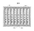
これを、液晶表示装置(液晶表示モジュールとも呼ばれる)の製品出荷時における梱包状態を示す図8の説明図を用いて説明する。
【0089】
図8において、BXは搬送用段ボール箱(例えば、通箱)、PKGはパッキング(緩衝)部材、VYNはビニル袋、MDLは液晶表示モジュール(上述の液晶表示装置製品)である。図示された液晶表示モジュールMDLは、第3筐体3に回路素子保護用の突起31を設ける本発明を採用したものである(図7(a)に表示のものを、複数個、縮小し、かつ、90度回転させて図示している)。
【0090】
搬送用段ボール箱BXの内壁にはパッキング部材PKGとして、ウレタンフォーム等のクッション材が用いられている。液晶表示モジュールMDLは一体毎にビニル袋VYNに入れられ、搬送用段ボール箱BX内に収められている。液晶表示モジュールMDL間にもパッキング部材PXが挿入されているが、これには段ボールの板紙が用いられることが多い。
【0091】
このような梱包形態において、各液晶表示モジュールMDL(の第3筐体3)に形成された突起31は、これらの間に挿入されるパッキング部材PXの撓みを抑え、撓んだパッキング部材PXがこれらの各々に搭載される電気回路素子を圧迫し破損することを防ぐ。
【0092】
上述のように、液晶表示パネル4に含まれる基板441、442(液晶表示基板とも呼ぶ)の主面に沿った第3筐体3の広さは第1筐体1および第2筐体2のそれより小さい。このため、上記突起31を第3筐体3に設けることは、その位置を保護すべき電気回路素子の近くに設けられるという利点をもたらす。仮に突起31を第1筐体1や第2筐体2に設けた場合、突起31の位置は上記電気回路素子から離れる。この離れた分だけ、突起31の位置から電気回路素子の位置の間でパッキング部材PXが撓む。このような観点から、突起31を第3筐体3に設けることにより電気回路素子の破損を確実に防げることは明らかであろう。
【0093】
なお、上記タイミング・コンバータ基板7や光源制御回路基板8に搭載される上記変圧素子72、81は、フェライト・コア等の部材を含め構成される。変圧機能にもよるが、多くの場合、タイミング・コンバータ基板7や光源制御回路基板8に搭載される素子の中で、変圧素子は最も高さが高い。また、これらの変圧素子は、レジン(樹脂材料)でモールドされた半導体のIC(集積回路素子)に比べて機械的な衝撃に弱いと言われている。上述の突起31の高さの設定では、これを除いた液晶表示装置の厚さを決める(換言すれば、第3筐体3の上面33に対し、最も背の高い)素子の上端より高くするとよいと述べた。しかし、搬送時の素子の破損のみに着眼すれば、第3筐体3の上面33上に搭載される変圧素子の中で最も高いものの上端より突起31を高く設定してもよい(例えば、他の半導体ICより低くても)。このような突起31の高さの設定は、各液晶表示装置の仕様(搭載する電気回路素子のバリエーション)に応じて、その基準を変えても良い。
【0094】
以上の説明では、突起31を第3筐体3の上面33に形成したが、その側面34に一部切り欠きをいれ、これをその一端が上面33より高い位置(図7のレイアウトで)に来るように折り曲げても良く、エプロン32に設けても良い(上記タイミング・コンバータ基板7や光源制御回路基板8のレイアウトに応じて適宜、位置を変えても良い)。
【0095】
《光源ユニットの保守》
液晶表示装置の組み立て(第3筐体3の第2筐体2への固定)の項目ですでに述べたが、本発明ではその第2の構成として、第3筐体3と第2筐体2との固定を第1筐体1と第2筐体2との固定とは別に行っている。この構成は、液晶表示装置製品(液晶表示モジュール)の光源ユニットの保守における負担を軽減する効果を奏する。
【0096】
図9は、本発明による第2の構成の説明図で、(a)液晶表示装置から光源ユニット(これが据え付けられた第3筐体3)を外した状態を示す図、(b)は(a)の円内に示す構造の拡大図である。図9(a)は、図3(h)および図3(i)を上下に反転させた構造に等しい。
【0097】
先述のように、第3筐体3の他端(データ駆動ICが配列されない周縁)のテラス32は、第1筐体1のテラス15と第2筐体2のテラス221とが形成する凹部に嵌められている。第3筐体の一端(データ駆動ICが配列される周縁)のテラス32を第2筐体のテラス22に固定する螺子322を外すと、第3筐体の一端は図9(a)に示されるように持ち上げられる。第3筐体3の他端のテラス32は一端のテラスに比べて側面34からのその端部までの距離が短いため、第3筐体の一端の持ち上げに応じて、上記凹部にて動ける。第3筐体3は、その一端をある程度持ち上げた段階で、第2筐体2(液晶表示モジール本体MDL)から外すことができる。
【0098】
液晶表示モジュールMDLから外された第3筐体3は、その上面33(タイミング・コンバータ基板7等が搭載された面)を下側に向けて(作業台等に向けて)置き、光源ユニットの保守や部品交換を行う。例えば、点灯性能の落ちた冷陰極管61が交換される。図示された第3筐体3は、先述の本発明の第1の構造に係る突起31を有するが、これを設けないときは、例えば、第3筐体3の両端のテラス32を把持する治具を用意し、作業台や机に第3筐体3の上面33に据え付けられたタイミング・コンバータ回路や光源制御回路の部品が当たらないようにする。
【0099】
図9から明らかなように、液晶表示パネル4や光学シート5という光源ユニットのメンテナンスの対象外の部品は液晶モジュール本体MDLに固定したまま、当該メンテナンス作業を行うことができることである。仮に、光源ユニットのメンテナンスにおいて第1筐体1と第2筐体2とを離すとなると、液晶表示パネル4や光学シート5の着脱、特にメンテナンス終了後の位置合わせに膨大な時間を要する。光学シート5に関しては、その仕様にもよるが、液晶表示パネル4との位置合わせの如何、ならびに位置合わせ作業中に液晶表示パネルと光学シートとの間に紛れ込む塵埃等により、表示画像の質が大きく影響される。
【0100】
本発明の第2の構造は、上述の液晶表示モジュールMDLをパーソナル・コンピュータ、液晶表示モニタ、またはテレビ等のセット製品に搭載した状態でも、そのユーザまたはこの製品のメンテナンス・エンジニアによる当該製品の保守・点検の負担を軽減する。
【0101】
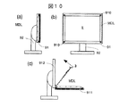
図10は、本発明による第2の構造を具体化した液晶表示装置を用いたモニタの一例を示す。図10の(a)は側面図、(b)は前面図(モニタ、すなわちユーザ側から見た図)、および(c)はこのモニタにおいて光源ユニットを外す状態を示す側面図である。
【0102】
液晶表示モニタ9は、画像表示部91と液晶表示部支持台92とからなり、前者はさらに、画像表示部前箱911、画像表示部後箱912からなる。液晶表示部支持台には、図示はしないが外部から供給される電力(例えば、100V)を液晶表示モニタ内の共通の電圧(例えば、12V)に変換する電源ユニットや、外付けのコンピュータからの信号を受けるインタフェース回路が搭載されている。
【0103】
上述の液晶表示モジュールMDLは、上記画像表示部前箱911の内部に螺子910で固定されている(図10(b)において液晶表示モジュールMDLの輪郭は破線で示されている)。螺子910は、液晶表示モジュールMDLの第1筐体1および第2筐体2のいずれか一方または双方を貫通し、これまたはこれらを画像表示部前箱911の内壁に固定する。螺子910は、液晶表示モジュールMDLの第3筐体3に到達しない長さのものを用いるか、またはこの螺子910が到達する部分において当該第3筐体3を部分的に凹ませるなどの工夫をする。この螺子910により、第3筐体3が第2筐体2より外せなくなることを防ぐためである。
【0104】
図10(c)に示すように、この液晶表示モニタの液晶表示モジュールの光源ユニットのメンテナンスは、画像表示部前箱911を液晶表示部支持台92に固定された画像表示部後箱912から開けて液晶表示モジュールMDLの背面(第3筐体3の上面側)を出し、後は図9を参照した上述の説明と同じ要領で、行うことができる。
【0105】
以上、本発明を実施の形態に基づいて具体的に説明したが、本発明は前記実施の形態に限定されるものではなく、その要旨を逸脱しない範囲において種々変更可能であることは勿論である。
【0106】
【発明の効果】
以上説明したように、本発明によれば、液晶表示装置の部品機種を共通化させることで、多品種化が進むコンピュータ・メーカやテレビ・メーカの商品に安定に柔軟に対応することができる。また、コンピュータならびにそのディスプレイ・モニタ、およびテレビジョンに搭載される液晶表示装置のメンテナンスを簡略化し、メンテナンス時における光源ユニットと液晶表示パネルとの位置調整を省くことができる。
【図面の簡単な説明】
【図1】本発明による液晶表示装置の分解斜視図(液晶表示パネル側から見た図)。
【図2】本発明による液晶表示装置の分解斜視図(液晶表示装置の裏側、すなわち図1の反対側から見た図)。
【図3】図1の右側面(III方向)から見た本発明による液晶表示装置の組立図(a)〜(g)、透視図(h)、および外観図(i)。
【図4】図1の左側面(IV方向)から見た本発明による液晶表示装置の透視図。
【図5】図1の前面(V方向)から見た本発明による液晶表示装置の組立図(a)〜(c)、および透視図(d)。
【図6】図2の上面(すなわち、液晶表示装置の裏側)から見た本発明による液晶表示装置の外観図。
【図7】本発明による第1の構成の説明図で、(a)液晶表示装置に光源駆動回路を設けた場合と、(b)設けない場合とを示す。
【図8】液晶表示装置の出荷時における梱包状態を示す説明図。
【図9】本発明による第2の構成の説明図で、(a)液晶表示装置から光源ユニットを外した状態を示す図、(b)(a)の円内に示す構造の拡大図。
【図10】本発明による液晶表示装置を用いたモニタの一例を示し、(a)側面図、(b)前面図(モニタ、すなわちユーザ側から見た図)、および(c)このモニタにおいて光源ユニットを外す状態を示す側面図。
【図11】液晶表示装置のマトリクス部とその周辺を含む回路図。
【符号の説明】
1…第1筐体、2…第2筐体、3…第3筐体、4…液晶表示パネル、5…光学シート、7…タイミング・コンバータ基板、8…光源制御回路基板、9…モニタ、11…開口(液晶表示窓)、12…第1筐体の上面、13…第1筐体の穴、14…切り欠き、15…第1筐体のテラス、16…第1筐体の下面、21…第2筐体の開口、22…第2筐体のテラス、23…第2筐体の穴、24…第2筐体の凸部、25…第2筐体の上面(LCD基板受け)、26…突起、31…突起、32…テラス面、33…上面、34…側面、41…ゲート駆動IC、42…ドレイン駆動IC、43…フレキシブル・プリント基板、61…冷陰極管、62…コネクタ(高圧側)、63…コネクタ(低圧側)、64、65…枠、71…タイミング・コンバータ・LSI、72…変圧素子(フェライト・コア)、73…コネクタ(ポート)、74…螺子、81…変圧素子、82…螺子、91…画像表示部、92…液晶表示支持部、221…テラス、261…開口、321、331…エプロン、333…ハンガ、334…螺子、341…開口、335…開口、411、421…プリント基板、441、442…LCD基板、631…ケーブル(低圧側)、641、651…ゴムブッシュ、642…溝、643…螺子、911…画像表示部前箱、912…画像表示部後箱、BX…搬送用段ボール箱、PKG…パッキング(緩衝)部材、VYN…ビニル袋、MDL…液晶表示モジュール、Tcon…タイミング・コンバータ回路、SC…画像表示領域、PX…画素、CLC…液晶層(セル)の容量、CS…画素の付加容量、GATE−DRV…ゲート信号駆動回路、GL…ゲート信号線(走査信号線)、DATA−DRV…データ信号駆動回路、DL…データ信号線(映像信号線)、Vcom…コモン(対向)電圧電源、CL…コモン(対向)電圧信号線。[0001]
BACKGROUND OF THE INVENTION
The present invention relates to a liquid crystal display device used as a monitor for a laptop personal computer, a desktop computer or the like, and a liquid crystal display monitor using the same.
[0002]
[Prior art]
Liquid crystal display devices have become widespread as monitors for laptop personal computers and desktop computers.
[0003]
In such products, the liquid crystal display device is mounted as a so-called liquid crystal display module in which a liquid crystal display panel and its light source are combined. The form is described in, for example, Japanese Patent Laid-Open Nos. 5-264911 and 7-218914.
[0004]
[Problems to be solved by the invention]
In products such as laptop personal computers and desktop computer monitors, products have been diversified in recent years.
[0005]
That is, in the situation where these products are produced in a variety of small quantities, the shapes of the liquid crystal display devices have been diversified.
[0006]
On the other hand, in order to stably supply the liquid crystal display device, it has been an issue to reduce the types of components (first issue).
[0007]
Moreover, in the situation where the use time of a monitor of a laptop personal computer or a desktop computer increases, it is required to reduce the burden related to the maintenance of these products (second problem). That is, an increase in the use time of the computer product by the office and individuals increases the burden on the light source unit of the liquid crystal display device, particularly the cold cathode tube used therefor, and causes unexpected deterioration thereof.
[0008]
Furthermore, in the situation where the number of computer manufacturers increases, it has become important to efficiently supply the liquid crystal display devices to these manufacturers. In this situation, it is important to reduce as much as possible the probability of breakage of the liquid crystal display device in transporting the liquid crystal display device to the computer manufacturer.
[0009]
However, in a situation where the liquid crystal display device is thinned and the performance of the control device is increasing, it is difficult to reduce the breakage year after year. Further, in a situation where the production of liquid crystal display devices tends to be a small variety and a variety of products, there is a greater possibility that the supply of a specific type of liquid crystal display device must be stopped due to the above-mentioned problems such as damage.
[0010]
A first object of the present invention is to stably and flexibly cope with the products of computer manufacturers and television manufacturers, which are becoming more diverse, by sharing the component models of liquid crystal display devices.
[0011]
The second object of the present invention is to simplify the maintenance of a liquid crystal display device mounted on a computer and its display monitor and television, and preferably eliminates the positional adjustment between the light source unit and the liquid crystal display panel during the maintenance, Another object is to prevent particles such as dust from entering the gap between the liquid crystal display panel and the optical sheet adjacent thereto.
[0012]
[Means for Solving the Problems]
In order to solve the above-described problems, the present invention provides a first, second, and third housing, a liquid crystal display panel fixed between the first and second housings, and the third housing. In a liquid crystal display device having a fixed light source and configured by overlapping the first, second, and third casings, the second casing and the third casing are detachable, and a timing converter board Is fixed to the surface of the third housing opposite to the surface on which the light source is disposed, and the surface of the timing converter substrate opposite to the surface on which the third housing is disposed is transformed. The elements are arranged, What is the side of the third housing on which the light source is arranged? A protrusion for protecting the components of the timing converter board is formed on the opposite surface, and the protrusion protrudes from the transformer element.
[0013]
Further, the protrusion is formed inside the periphery of the liquid crystal display device.
[0014]
Further, a light source control circuit is disposed on the opposite surface.
[0017]
The first housing, the second housing, and the third housing described above are formed on the main surface of a substrate (for example, a member referred to as a liquid crystal display substrate or a transparent substrate) included in the liquid crystal display panel, for example. A first member (main surface member, plate) is included. When the periphery of the image display area of the liquid crystal display device is narrowed, the first member of the first casing and the second casing has its surface occupied by an opening exposing the liquid crystal display panel, and has a so-called frame shape. Present. The outlines of these first members are changed in the order of, for example, a first casing, a second casing, and a third casing, and the liquid crystal display device has an outline of the first member of one casing and the other. The first member of the casing is assembled so as to overlap the outline of the first member. In addition, at least one of the first housing, the second housing, and the third housing described above is a second member (side member) protruding in the thickness direction of the substrate from one surface or the periphery of the first member. , Side). Depending on the use of the liquid crystal display device, the second member may be integrally formed so as to surround at least a part of the one surface of the first member, or an intermittent part such as a notch may be provided on at least a part of the second member. There is also. The second member also serves as a guide for overlapping two of the first to third housings.
[0018]
The “thickness (maximum thickness)” of the liquid crystal display device in the present invention is defined as a dimension in the thickness direction of the substrate (the protruding direction of the second member). The height of the protrusion is also defined as a dimension in the thickness direction of the substrate. The definition of this shape will be described in detail later with reference to the drawings. The third housing may be provided with a plurality of the protrusions spaced apart from each other, or a wall formed as the protrusion may be a part of the first member of the third housing (for example, the component is You may form so that the part to be mounted) may be surrounded.
[0019]
In the present invention, by sharing the component models of the liquid crystal display device, it is possible to stably and flexibly cope with the products of computer manufacturers and television manufacturers that are becoming more diverse. Further, the maintenance of the liquid crystal display device mounted on the computer and its display / monitor and television can be simplified, and the position adjustment between the light source unit and the liquid crystal display panel during the maintenance can be omitted. Alternatively, when an optical sheet is provided in the second casing adjacent to the liquid crystal display panel, it is not necessary to remove the first casing and the second casing, so that dust may be generated between the liquid crystal display panel and the optical sheet. Deterioration of the optical characteristics of the liquid crystal display device due to entering can be prevented.
[0020]
DETAILED DESCRIPTION OF THE INVENTION
Hereinafter, embodiments of the present invention will be described in detail with reference to the drawings. In the drawings described below, components having the same function are denoted by the same reference numerals, and repeated description thereof is omitted.
[0021]
<Overall configuration of liquid crystal display device>
1 and 2 are exploded perspective views of a liquid crystal display device according to the present invention.
[0022]
1 is a perspective view from the liquid crystal display panel side (front side with respect to the user's field of view of the liquid crystal display device), and FIG. 2 is a perspective view from the opposite side of FIG. Each is depicted as a diagram.
[0023]
In FIG. 1, 1 is a first housing, 2 is a second housing, 3 is a third housing, 4 is a liquid crystal display panel, 5 is an optical sheet (a diffusion film on the light source side, a prism film on the display panel side), and 61 Cold cathode tube, 7 is a timing converter board, 8 is a light source control circuit board constituting a light source control circuit, 11 is an opening (liquid crystal display window) of the
[0024]
In FIG. 2, 31 is a protrusion provided on the
[0025]
The liquid crystal display device fixes the liquid
[0026]
FIG. 3 is a detailed assembly view of the liquid crystal display device as viewed from the III direction in FIG. 1 and the assembled view thereof. FIG. 4 is a perspective view of the liquid crystal display device as viewed from the IV direction in FIG. FIG. 5 shows a conceptual assembly diagram of the liquid crystal display device viewed from the direction V in FIG. 1 and a diagram after assembly. FIG. 6 shows an assembled view (back view of the liquid crystal display device with respect to the field of view of the user of the liquid crystal display device) overlooking FIG. It should be noted that FIGS. 3 to 6 are partially modified for the sake of explanation with respect to FIGS. 1 and 2. For example, in FIG. 1 and FIG. 2, the number of the
[0027]
In FIG. 3A, 12 is the upper surface of the
[0028]
In (b), 411 and 421 are printed circuit boards, and 441 and 442 are LCD boards.
[0029]
In (c), 25 is the upper surface (LCD substrate holder) of the
[0030]
In (e), 642 is a groove provided in the holding
[0031]
In (f), 333 is a hanger.
[0032]
In (g), 71 is a timing converter LSI, 72 is a transformer element (ferrite core), and 73 is a connector (port).
[0033]
In (h), 631 is a cable (low pressure side).
[0034]
In (i), MDL is a liquid crystal display module.
[0035]
In FIG. 4,
[0036]
In FIG. 5, 74 is a screw for fixing the
[0037]
<<
As shown in FIG. 3B, the liquid
[0038]
FIG. 11 is an outline of a liquid crystal display device, that is, a connection diagram of an equivalent circuit of a display matrix section and its peripheral circuits.
[0039]
Tcon is a timing converter circuit, SC is an image display area, PX is a pixel, C LC Is the capacity of the liquid crystal layer (cell), C S Is a gate signal drive circuit, GL is a gate signal line (scanning signal line), DATA-DRV is a data signal drive circuit, DL is a data signal line (video signal line), and Vcom is a common ( A counter (voltage) power supply CL is a common (counter) voltage signal line.
[0040]
The liquid
[0041]
A gate signal line GL is connected to the gate electrode of the symbol of the field effect transistor, and a signal is supplied from the gate signal drive circuit GATE-DRV. The gate signal lines GL are arranged in parallel on the
[0042]
On the other hand, one end of the electrical path that is opened and closed by the switching element TFT has a capacitance C across the liquid crystal layer. LC One end of the pair of electrodes forming the (referred to as pixel electrode) and the other end is connected to the data signal line DL. For example, a plurality of data signal lines DL are arranged in parallel on the
[0043]
The data signal line DL and the gate signal line GL extend in a direction crossing each other, and are electrically separated from each other above and below an insulating film (for example, the gate insulating film of the field effect transistor) on the
[0044]
In the pixel PX of FIG. 11, a capacitor C is sandwiched between the liquid crystal layers. LC A predetermined voltage is applied from the voltage source Vcom through the counter voltage signal line CL to the other of the pair of electrodes (called a counter electrode and a common electrode). In addition, a capacitance C across the liquid crystal layer LC In order to prevent the potential difference between the electrodes forming the capacitor from changing while the switching element TFT is closed, the additional capacitor C S Is formed. This additional capacity C S For example, the pixel electrode and the counter electrode are configured to face each other with a dielectric (such as the gate insulating film) other than the liquid crystal layer. Among liquid crystal display devices, many of the types called TN type (twisted nematic type) are arranged such that the pixel electrode and the counter electrode face each other with the liquid crystal layer interposed therebetween, and the IPS type (in-plane switching type) or In many types called FFS type (fringe field type), the pixel electrode and the counter electrode are arranged on the same substrate. In the case of the TN type, for example, a pixel electrode is separately provided for each pixel PX on the
[0045]
In the case of an active matrix type liquid crystal display device, switching elements TFTs of a plurality of pixels PX along each of the gate signal lines GL are selected and opened for each gate signal line GL, and data signals are time-divided into individual gates. This is supplied to the pixels along the signal line GL. A circuit for controlling this is called a timing converter circuit Tcon. The timing converter circuit Tcon generates, for example, a clock signal for the time division control, and supplies a liquid crystal driving voltage applied to the liquid crystal layer corresponding to each pixel PX. A circuit having a function similar to this is also used for a passive matrix liquid crystal display device (typified by an STN (super twist nematic) liquid crystal display device). Therefore, the timing converter circuit Tcon is positioned as a liquid crystal drive control and power supply circuit.
[0046]
The timing converter circuit Tcon is formed on the timing converter board 7 (printed board) shown in FIGS. 1 to 6, and is the back surface (upper surface in FIG. 2) as viewed from the user of the liquid crystal display device of the
[0047]
As described above, the timing converter circuit Tcon not only generates a signal for image display control but also supplies a data signal voltage to be applied to the liquid crystal layer. For example, a power supply voltage of 12V is supplied to the liquid crystal display device (even if an AC voltage of 100V is supplied from an external power supply, it is once converted into a predetermined power supply voltage value). On the other hand, the voltage of the driving IC connected to the gate signal line GL and the data signal line DL is 3V to 5V. On the other hand, the voltage applied to the liquid crystal layer by the pixel electrode in the individual pixel PX is, for example, in the range of 5V to 10V, depending on the type of liquid crystal composition used. Furthermore, in order to avoid polarization of the liquid crystal layer during the control of the liquid crystal layer, it is necessary to reverse the polarity with respect to the potential of the counter electrode. Therefore, the voltage supply to the pixel electrode is required to realize a voltage fluctuation of a range of twice the applied voltage to the liquid crystal layer, for example, 10V to 20V. For this reason, in the
[0048]
In the active matrix type liquid crystal display device, the gate signal driving circuit GATE-DRV shown in FIG. 11 includes a plurality of
[0049]
Through this flexible printed
[0050]
<< Storage of
The liquid
[0051]
Although not shown, an image display area SC schematically shown in FIG. 11 is formed on the upper surface of the liquid
[0052]
The lower surface (upper surface in FIG. 2) of the liquid
[0053]
In this manner, the
[0054]
The liquid
[0055]
At this time, a cutout on the side surface of the
[0056]
As shown in FIGS. 1, 3 (c) and 5 (b), a
[0057]
As shown in FIGS. 3C and 5B, in addition to the
[0058]
<< Assembling the optical unit (fixed to the third housing 3) >>
As shown in FIGS. 1, 2, and 3 (e), the
[0059]
In this embodiment, a plurality of
[0060]
On the
[0061]
In the light source
[0062]
The requirement for the specifications of the light source
[0063]
Therefore, the circuit pattern in the light source
[0064]
In contrast to the wiring on the high-voltage side of the
[0065]
As shown in FIG. 6, there is a so-called vacant space on the
[0066]
<< Assembly of liquid crystal display device (fixation of the
As described above, the
[0067]
As shown at the left end of FIG. 3 (h), the
[0068]
On the other hand, on the right side of FIG. 3 (h), a
[0069]
On the right side of FIG. 3 (h), without forming the concave portion by the
[0070]
On the other hand, when screwing the
[0071]
The
[0072]
The
[0073]
<< Setting of the
Although it does not stand out in the appearance shown in FIG. 3 (i), the upper end of the
[0074]
If the elements fixed to the housing protrude from the assembled housing, the elements are damaged when the liquid crystal display device is mounted on a so-called set product such as the personal computer, the liquid crystal display monitor, or the television set. The possibility comes out. The same possibility arises when the liquid crystal display device is transported to the manufacturer of the set product described above.
[0075]
In order to protect the elements (electronic parts and the like) fixed to the casing constituting the liquid crystal display device from the above-described damage, the present invention provides the
[0076]
As described above, the
[0077]
Moreover, since the 1st housing |
[0078]
For this reason, it is arranged on the
[0079]
FIG. 7 is an explanatory diagram of the first configuration according to the present invention. FIG. 7A shows a vertically inverted liquid crystal display device shown in FIG. In the following description, the dimension of the liquid crystal display device along the vertical direction in FIG. 7 is referred to as “thickness” or “height”, and the dimension of the liquid crystal display device along the direction transverse to FIG. Expressed as “area”.
[0080]
Assuming that there is no
[0081]
Depending on the set product manufacturer, a light source drive circuit may be provided in the body of a set product such as a personal computer, and the liquid crystal display device may be used without the light source
[0082]
In this case, only the members of the
[0083]
As is apparent from the above description, there is a possibility that the dimensions of the housing may change considerably depending on whether or not the light source control circuit is mounted on the liquid crystal display device on which the liquid
[0084]
One is that a line for manufacturing two types of liquid crystal display device products that differ only in the presence or absence of the light source control circuit must be provided separately from the mounting of the liquid
[0085]
The other is that when the assembly of the
[0086]
When the production of two types of liquid crystal display device products is dealt with in the shape of the
[0087]
Furthermore, the present invention also has the following advantages in transporting liquid crystal display device products.
[0088]
This will be described with reference to the explanatory view of FIG. 8 showing the packaging state of the liquid crystal display device (also referred to as a liquid crystal display module) at the time of product shipment.
[0089]
In FIG. 8, BX is a cardboard box for conveyance (for example, a box), PKG is a packing (buffer) member, VYN is a vinyl bag, and MDL is a liquid crystal display module (the above-mentioned liquid crystal display device product). The illustrated liquid crystal display module MDL employs the present invention in which the
[0090]
A cushioning material such as urethane foam is used as a packing member PKG on the inner wall of the cardboard box BX for conveyance. The liquid crystal display module MDL is put into a vinyl bag VYN for each unit and is housed in a cardboard box BX for transport. A packing member PX is also inserted between the liquid crystal display modules MDL, and cardboard board is often used for this.
[0091]
In such a packing form, the
[0092]
As described above, the width of the
[0093]
The
[0094]
In the above description, the
[0095]
<Maintenance of light source unit>
As already described in the item of assembling the liquid crystal display device (fixing the
[0096]
FIG. 9 is an explanatory diagram of the second configuration according to the present invention. FIG. 9A is a diagram showing a state in which the light source unit (the
[0097]
As described above, the
[0098]
The
[0099]
As is apparent from FIG. 9, the maintenance work can be performed while the liquid
[0100]
According to the second structure of the present invention, even when the above-mentioned liquid crystal display module MDL is mounted on a set product such as a personal computer, a liquid crystal display monitor, or a television, the user or a maintenance engineer of the product maintains the product.・ Reduce the burden of inspection.
[0101]
FIG. 10 shows an example of a monitor using a liquid crystal display device embodying the second structure according to the present invention. 10A is a side view, FIG. 10B is a front view (a monitor, ie, a view seen from the user side), and FIG. 10C is a side view showing a state in which the light source unit is removed from the monitor.
[0102]
The liquid crystal display monitor 9 includes an
[0103]
The above-mentioned liquid crystal display module MDL is fixed inside the image display
[0104]
As shown in FIG. 10C, the maintenance of the light source unit of the liquid crystal display module of this liquid crystal display monitor is performed by opening the image display
[0105]
The present invention has been specifically described above based on the embodiments. However, the present invention is not limited to the above-described embodiments, and various modifications can be made without departing from the scope of the invention. .
[0106]
【The invention's effect】
As described above, according to the present invention, by sharing the component models of the liquid crystal display device, it is possible to stably and flexibly cope with products of computer manufacturers and television manufacturers that are becoming more diverse. Further, the maintenance of the liquid crystal display device mounted on the computer and its display / monitor and television can be simplified, and the position adjustment between the light source unit and the liquid crystal display panel during the maintenance can be omitted.
[Brief description of the drawings]
FIG. 1 is an exploded perspective view of a liquid crystal display device according to the present invention (viewed from a liquid crystal display panel side).
FIG. 2 is an exploded perspective view of the liquid crystal display device according to the present invention (viewed from the back side of the liquid crystal display device, that is, the opposite side of FIG. 1).
3 is an assembly diagram (a) to (g), a perspective view (h), and an external view (i) of the liquid crystal display device according to the present invention as viewed from the right side surface (III direction) of FIG.
4 is a perspective view of the liquid crystal display device according to the present invention viewed from the left side (IV direction) of FIG.
FIGS. 5A and 5B are assembly views (a) to (c) and a perspective view (d) of the liquid crystal display device according to the present invention as viewed from the front surface (V direction) of FIG. 1;
6 is an external view of the liquid crystal display device according to the present invention as viewed from the upper surface of FIG. 2 (that is, the back side of the liquid crystal display device).
FIGS. 7A and 7B are explanatory diagrams of a first configuration according to the present invention, showing (a) a case where a liquid crystal display device is provided with a light source driving circuit and (b) a case where it is not provided.
FIG. 8 is an explanatory diagram showing a packaging state at the time of shipment of the liquid crystal display device.
FIGS. 9A and 9B are explanatory diagrams of a second configuration according to the present invention, in which FIG. 9A shows a state in which a light source unit is removed from a liquid crystal display device, and FIG.
FIGS. 10A and 10B show an example of a monitor using a liquid crystal display device according to the present invention, in which FIG. 10A is a side view, FIG. 10B is a front view (monitor, ie, a view seen from the user side), and FIG. The side view which shows the state which removes a unit.
FIG. 11 is a circuit diagram including a matrix portion of a liquid crystal display device and its periphery.
[Explanation of symbols]
DESCRIPTION OF
Claims (5)
上記第1、第2、第3筐体を重ねて構成した液晶表示装置において、
上記第2筐体と上記第3筐体は着脱可能であり、
タイミング・コンバータ基板を上記第3筐体の上記光源を配置した側とは反対側の面に固定し、さらに該タイミング・コンバータ基板の上記第3筐体が配置されている面とは反対側の面には変圧素子が配置されており、
上記第3筐体の上記光源を配置した側とは反対側の面に上記タイミング・コンバータ基板の部品保護用の突起を形成し、該突起は上記変圧素子よりも突出して形成されていることを特徴とする液晶表示装置。A liquid crystal display panel fixed between the first, second, and third housings, the first and second housings, and a light source fixed on the third housing;
In the liquid crystal display device configured by overlapping the first, second, and third housings,
The second housing and the third housing are detachable,
The timing converter board is fixed to a surface of the third casing opposite to the side where the light source is disposed, and further, the timing converter board is disposed on a side opposite to the surface where the third casing is disposed. Transformer elements are arranged on the surface,
Protrusions for protecting the components of the timing converter board are formed on the surface of the third housing opposite to the side where the light source is disposed, and the protrusions are formed so as to protrude from the transformer element. A characteristic liquid crystal display device.
Priority Applications (10)
| Application Number | Priority Date | Filing Date | Title |
|---|---|---|---|
| JP27884499A JP3919982B2 (en) | 1999-09-30 | 1999-09-30 | Liquid crystal display device and liquid crystal display monitor |
| US09/671,429 US6992734B1 (en) | 1999-09-30 | 2000-09-27 | Liquid crystal display device |
| TW089120010A TWI287140B (en) | 1999-09-30 | 2000-09-27 | Liquid crystal display device |
| KR10-2000-0057004A KR100387108B1 (en) | 1999-09-30 | 2000-09-28 | Liquid crystal display device |
| US11/252,848 US7432997B2 (en) | 1999-09-30 | 2005-10-19 | Liquid crystal display device |
| US11/808,682 US7542106B2 (en) | 1999-09-30 | 2007-06-12 | Liquid crystal display device |
| US12/078,014 US7834950B2 (en) | 1999-09-30 | 2008-03-26 | Liquid crystal display device |
| US12/078,013 US20080180601A1 (en) | 1999-09-30 | 2008-03-26 | Liquid crystal display device |
| US12/153,744 US20080239196A1 (en) | 1999-09-30 | 2008-05-23 | Liquid crystal display device |
| US12/923,479 US8102482B2 (en) | 1999-09-30 | 2010-09-23 | Liquid crystal display device |
Applications Claiming Priority (1)
| Application Number | Priority Date | Filing Date | Title |
|---|---|---|---|
| JP27884499A JP3919982B2 (en) | 1999-09-30 | 1999-09-30 | Liquid crystal display device and liquid crystal display monitor |
Publications (2)
| Publication Number | Publication Date |
|---|---|
| JP2001100183A JP2001100183A (en) | 2001-04-13 |
| JP3919982B2 true JP3919982B2 (en) | 2007-05-30 |
Family
ID=17602947
Family Applications (1)
| Application Number | Title | Priority Date | Filing Date |
|---|---|---|---|
| JP27884499A Expired - Fee Related JP3919982B2 (en) | 1999-09-30 | 1999-09-30 | Liquid crystal display device and liquid crystal display monitor |
Country Status (4)
| Country | Link |
|---|---|
| US (7) | US6992734B1 (en) |
| JP (1) | JP3919982B2 (en) |
| KR (1) | KR100387108B1 (en) |
| TW (1) | TWI287140B (en) |
Families Citing this family (24)
| Publication number | Priority date | Publication date | Assignee | Title |
|---|---|---|---|---|
| JP2002311417A (en) * | 2001-04-17 | 2002-10-23 | Nec Corp | Liquid crystal display device |
| KR100955545B1 (en) * | 2002-03-28 | 2010-04-30 | 산요덴키가부시키가이샤 | Liquid crystal display |
| KR100854006B1 (en) * | 2002-04-15 | 2008-08-25 | 삼성전자주식회사 | Liquid crystal display |
| KR100873067B1 (en) * | 2002-07-11 | 2008-12-11 | 삼성전자주식회사 | Back light assembly and liquid crystal display device having the same |
| JP4084166B2 (en) | 2002-11-13 | 2008-04-30 | 株式会社 日立ディスプレイズ | Image display device |
| KR100890751B1 (en) * | 2002-12-26 | 2009-03-26 | 엘지디스플레이 주식회사 | Coupling Structure of Liquid Crystal Display Device with Direct Backlight Unit |
| KR20050082643A (en) * | 2004-02-19 | 2005-08-24 | 삼성에스디아이 주식회사 | Driving method of fs-lcd |
| JP3852707B2 (en) * | 2004-07-27 | 2006-12-06 | 船井電機株式会社 | LCD module |
| JP4517763B2 (en) * | 2004-08-03 | 2010-08-04 | 船井電機株式会社 | Liquid crystal display |
| JP4036228B2 (en) * | 2005-06-20 | 2008-01-23 | 船井電機株式会社 | Liquid crystal display |
| CN100493310C (en) * | 2006-01-11 | 2009-05-27 | 中强光电股份有限公司 | Easy-to-disassemble pressure-relief fastener |
| CN100561313C (en) * | 2006-07-05 | 2009-11-18 | 鸿富锦精密工业(深圳)有限公司 | Backlight module and its lamp tube fixing frame |
| JP4881678B2 (en) * | 2006-09-04 | 2012-02-22 | 株式会社 日立ディスプレイズ | Liquid crystal display |
| JP2008216347A (en) * | 2007-02-28 | 2008-09-18 | Sony Corp | Display device |
| US8144288B2 (en) * | 2007-09-20 | 2012-03-27 | Sharp Kabushiki Kaisha | Display unit and television receiver |
| US8064005B2 (en) * | 2008-07-31 | 2011-11-22 | Samsung Electronics Co., Ltd. | Light supplying unit and display device using the same |
| KR101157352B1 (en) * | 2008-11-26 | 2012-07-03 | 엘지디스플레이 주식회사 | Liquid crystal display device |
| KR101294850B1 (en) * | 2008-11-27 | 2013-08-08 | 엘지디스플레이 주식회사 | Liquid Crystal Display |
| TWI360038B (en) * | 2008-12-09 | 2012-03-11 | Compal Electronics Inc | Electronic device |
| AU2010296605A1 (en) * | 2009-09-16 | 2012-04-05 | Sharp Kabushiki Kaisha | Lighting device, display apparatus, and television receiver |
| JP2012078415A (en) * | 2010-09-30 | 2012-04-19 | Hitachi Displays Ltd | Display device |
| US9195331B2 (en) * | 2011-12-06 | 2015-11-24 | Apple Inc. | Common electrode connections in integrated touch screens |
| CN104633521A (en) * | 2013-11-06 | 2015-05-20 | 富泰华精密电子(郑州)有限公司 | Backlight module |
| PL3187647T3 (en) * | 2015-12-29 | 2022-06-13 | Electrolux Appliances Aktiebolag | Household appliance with an electronic board and method for manufacturing a household appliance |
Family Cites Families (37)
| Publication number | Priority date | Publication date | Assignee | Title |
|---|---|---|---|---|
| US5293262A (en) * | 1988-03-15 | 1994-03-08 | Mitsubishi Denki Kabushiki Kaisha | Liquid crystal display device having heat-insulating members and driving circuit boards attached to rear edges of light box |
| JP2875327B2 (en) * | 1990-03-02 | 1999-03-31 | 株式会社日立製作所 | Liquid crystal display |
| JPH052164A (en) * | 1991-01-28 | 1993-01-08 | Toshiba Corp | Lcd module |
| US5809012A (en) * | 1991-01-31 | 1998-09-15 | Fujitsu Limited | Connectionless communication system |
| JPH0519228A (en) * | 1991-07-15 | 1993-01-29 | Hitachi Ltd | Liquid crystal display device module |
| JPH05119311A (en) | 1991-10-24 | 1993-05-18 | Nec Corp | Back light |
| JP3063331B2 (en) | 1991-12-18 | 2000-07-12 | 株式会社日立製作所 | Liquid crystal display |
| JP2797804B2 (en) * | 1992-01-09 | 1998-09-17 | 日本電気株式会社 | Backlight and liquid crystal display |
| JP3205373B2 (en) * | 1992-03-12 | 2001-09-04 | 株式会社日立製作所 | Liquid crystal display |
| JP3469907B2 (en) | 1992-03-12 | 2003-11-25 | 株式会社 日立ディスプレイズ | Liquid crystal display |
| JP3136200B2 (en) * | 1992-07-22 | 2001-02-19 | 株式会社日立製作所 | Liquid crystal display |
| JP3560164B2 (en) * | 1993-06-02 | 2004-09-02 | 株式会社 日立ディスプレイズ | Liquid crystal display |
| JP3222268B2 (en) * | 1993-06-02 | 2001-10-22 | 株式会社日立製作所 | Liquid crystal display |
| US5450221A (en) * | 1993-09-08 | 1995-09-12 | Delco Electronics Corporation | Compact liquid crystal display for instrument panel having a wrap around flexible printed circuit board and translucent web |
| JPH07199180A (en) | 1994-01-07 | 1995-08-04 | Hitachi Ltd | Liquid crystal display |
| JPH07218914A (en) | 1994-01-27 | 1995-08-18 | Casio Comput Co Ltd | Liquid crystal display device with back light |
| JPH0876118A (en) | 1994-09-09 | 1996-03-22 | Toshiba Corp | Light-transmissive display device |
| JPH0894845A (en) | 1994-09-27 | 1996-04-12 | Toshiba Lighting & Technol Corp | Light source device, backlight using the same, and liquid crystal display device |
| TW344043B (en) | 1994-10-21 | 1998-11-01 | Hitachi Ltd | Liquid crystal display device with reduced frame portion surrounding display area |
| JPH09175080A (en) * | 1995-12-13 | 1997-07-08 | Baineng Ind Co Ltd | Writing implement |
| JPH09318952A (en) | 1996-05-30 | 1997-12-12 | Hitachi Ltd | Liquid crystal display |
| US6275861B1 (en) * | 1996-09-27 | 2001-08-14 | Pmc-Sierra, Inc. | Method and apparatus to identify flows in data systems |
| JPH10105087A (en) * | 1996-09-30 | 1998-04-24 | Sony Corp | Flat display |
| JPH11126028A (en) | 1997-10-23 | 1999-05-11 | Hitachi Ltd | Liquid crystal display |
| US6272109B1 (en) * | 1997-11-18 | 2001-08-07 | Cabletron Systems, Inc. | Hierarchical schedules for different ATM traffic |
| US6279035B1 (en) * | 1998-04-10 | 2001-08-21 | Nortel Networks Limited | Optimizing flow detection and reducing control plane processing in a multi-protocol over ATM (MPOA) system |
| KR100319199B1 (en) * | 1998-09-24 | 2002-10-25 | 삼성전자 주식회사 | LCD Display |
| KR100333250B1 (en) * | 1998-10-05 | 2002-05-17 | 가나이 쓰토무 | Packet forwarding apparatus with a flow detection table |
| JP2000214461A (en) * | 1999-01-26 | 2000-08-04 | Hitachi Ltd | Liquid crystal display |
| JP3743194B2 (en) * | 1999-02-25 | 2006-02-08 | 株式会社日立製作所 | Packet relay device |
| JP3381687B2 (en) * | 1999-11-25 | 2003-03-04 | 日本電気株式会社 | Flow identification device, flow processing device, flow identification method, and flow processing method |
| JP3994614B2 (en) * | 2000-03-13 | 2007-10-24 | 株式会社日立製作所 | Packet switch, network monitoring system, and network monitoring method |
| KR100340440B1 (en) * | 2000-07-20 | 2002-06-12 | 구본준, 론 위라하디락사 | Lamp Apparatus For Liquid Crystal Display |
| US7042848B2 (en) * | 2001-05-04 | 2006-05-09 | Slt Logic Llc | System and method for hierarchical policing of flows and subflows of a data stream |
| JP3965283B2 (en) * | 2001-07-02 | 2007-08-29 | 株式会社日立製作所 | Packet transfer device with multiple types of packet control functions |
| JP2003018204A (en) * | 2001-07-02 | 2003-01-17 | Hitachi Ltd | Packet transfer device having flow detection function and flow management method |
| JP2003078549A (en) * | 2001-08-31 | 2003-03-14 | Hitachi Ltd | Packet transfer method and apparatus |
-
1999
- 1999-09-30 JP JP27884499A patent/JP3919982B2/en not_active Expired - Fee Related
-
2000
- 2000-09-27 US US09/671,429 patent/US6992734B1/en not_active Expired - Fee Related
- 2000-09-27 TW TW089120010A patent/TWI287140B/en not_active IP Right Cessation
- 2000-09-28 KR KR10-2000-0057004A patent/KR100387108B1/en not_active Expired - Fee Related
-
2005
- 2005-10-19 US US11/252,848 patent/US7432997B2/en not_active Expired - Fee Related
-
2007
- 2007-06-12 US US11/808,682 patent/US7542106B2/en not_active Expired - Fee Related
-
2008
- 2008-03-26 US US12/078,014 patent/US7834950B2/en not_active Expired - Fee Related
- 2008-03-26 US US12/078,013 patent/US20080180601A1/en not_active Abandoned
- 2008-05-23 US US12/153,744 patent/US20080239196A1/en not_active Abandoned
-
2010
- 2010-09-23 US US12/923,479 patent/US8102482B2/en not_active Expired - Fee Related
Also Published As
| Publication number | Publication date |
|---|---|
| US7834950B2 (en) | 2010-11-16 |
| US20080180601A1 (en) | 2008-07-31 |
| US8102482B2 (en) | 2012-01-24 |
| KR20010030527A (en) | 2001-04-16 |
| TWI287140B (en) | 2007-09-21 |
| US7542106B2 (en) | 2009-06-02 |
| JP2001100183A (en) | 2001-04-13 |
| US7432997B2 (en) | 2008-10-07 |
| US6992734B1 (en) | 2006-01-31 |
| US20070258021A1 (en) | 2007-11-08 |
| US20060038934A1 (en) | 2006-02-23 |
| US20110037921A1 (en) | 2011-02-17 |
| KR100387108B1 (en) | 2003-06-12 |
| US20080186426A1 (en) | 2008-08-07 |
| US20080239196A1 (en) | 2008-10-02 |
Similar Documents
| Publication | Publication Date | Title |
|---|---|---|
| JP3919982B2 (en) | Liquid crystal display device and liquid crystal display monitor | |
| US7567314B2 (en) | Flat panel display apparatus having fixing member to secure display module | |
| KR100266356B1 (en) | A flip-chip type liquid crystal display device employing a folded curved driving multi-layer flexible circuit board | |
| KR100577511B1 (en) | Display modules and display devices | |
| US7439553B2 (en) | Liquid crystal display device | |
| US20050073621A1 (en) | Liquid crystal display device | |
| JPH11305254A (en) | Liquid crystal display | |
| JP3576294B2 (en) | Liquid crystal display | |
| US8031291B2 (en) | Liquid crystal display and tablet computer having a chassis fastening member that receives a printed circuit board | |
| TW527503B (en) | Liquid crystal display device | |
| JPH11344696A (en) | Liquid crystal display | |
| JP2000047209A (en) | Liquid crystal display | |
| KR20060082471A (en) | Liquid crystal display | |
| KR101277217B1 (en) | Pcb fixing structure for liquid crystal display device | |
| JPH11305227A (en) | Liquid crystal display | |
| JP3958341B2 (en) | Liquid crystal display module and liquid crystal display device | |
| JPH11305226A (en) | Liquid crystal display | |
| JP3786992B2 (en) | Liquid crystal display | |
| JP2000019560A (en) | Liquid crystal display | |
| KR20060083262A (en) | Liquid crystal display | |
| KR20120113387A (en) | Flat panel display device and mathod for manufacturing the same | |
| KR20060116111A (en) | Back light assembly and liquid crystal display employing the same | |
| KR20070119330A (en) | LCD Display | |
| JPH11305208A (en) | Liquid crystal display |
Legal Events
| Date | Code | Title | Description |
|---|---|---|---|
| A977 | Report on retrieval |
Free format text: JAPANESE INTERMEDIATE CODE: A971007 Effective date: 20050930 |
|
| A131 | Notification of reasons for refusal |
Free format text: JAPANESE INTERMEDIATE CODE: A131 Effective date: 20060411 |
|
| A521 | Written amendment |
Free format text: JAPANESE INTERMEDIATE CODE: A523 Effective date: 20060609 |
|
| A131 | Notification of reasons for refusal |
Free format text: JAPANESE INTERMEDIATE CODE: A131 Effective date: 20061010 |
|
| A521 | Written amendment |
Free format text: JAPANESE INTERMEDIATE CODE: A523 Effective date: 20061211 |
|
| A131 | Notification of reasons for refusal |
Free format text: JAPANESE INTERMEDIATE CODE: A131 Effective date: 20070116 |
|
| A521 | Written amendment |
Free format text: JAPANESE INTERMEDIATE CODE: A523 Effective date: 20070122 |
|
| TRDD | Decision of grant or rejection written | ||
| A01 | Written decision to grant a patent or to grant a registration (utility model) |
Free format text: JAPANESE INTERMEDIATE CODE: A01 Effective date: 20070213 |
|
| A61 | First payment of annual fees (during grant procedure) |
Free format text: JAPANESE INTERMEDIATE CODE: A61 Effective date: 20070214 |
|
| R150 | Certificate of patent or registration of utility model |
Ref document number: 3919982 Country of ref document: JP Free format text: JAPANESE INTERMEDIATE CODE: R150 Free format text: JAPANESE INTERMEDIATE CODE: R150 |
|
| FPAY | Renewal fee payment (event date is renewal date of database) |
Free format text: PAYMENT UNTIL: 20100223 Year of fee payment: 3 |
|
| FPAY | Renewal fee payment (event date is renewal date of database) |
Free format text: PAYMENT UNTIL: 20110223 Year of fee payment: 4 |
|
| FPAY | Renewal fee payment (event date is renewal date of database) |
Free format text: PAYMENT UNTIL: 20110223 Year of fee payment: 4 |
|
| S531 | Written request for registration of change of domicile |
Free format text: JAPANESE INTERMEDIATE CODE: R313531 |
|
| FPAY | Renewal fee payment (event date is renewal date of database) |
Free format text: PAYMENT UNTIL: 20110223 Year of fee payment: 4 |
|
| R371 | Transfer withdrawn |
Free format text: JAPANESE INTERMEDIATE CODE: R371 |
|
| FPAY | Renewal fee payment (event date is renewal date of database) |
Free format text: PAYMENT UNTIL: 20110223 Year of fee payment: 4 |
|
| S111 | Request for change of ownership or part of ownership |
Free format text: JAPANESE INTERMEDIATE CODE: R313111 |
|
| S631 | Written request for registration of reclamation of domicile |
Free format text: JAPANESE INTERMEDIATE CODE: R313631 |
|
| FPAY | Renewal fee payment (event date is renewal date of database) |
Free format text: PAYMENT UNTIL: 20110223 Year of fee payment: 4 |
|
| R350 | Written notification of registration of transfer |
Free format text: JAPANESE INTERMEDIATE CODE: R350 |
|
| FPAY | Renewal fee payment (event date is renewal date of database) |
Free format text: PAYMENT UNTIL: 20120223 Year of fee payment: 5 |
|
| R250 | Receipt of annual fees |
Free format text: JAPANESE INTERMEDIATE CODE: R250 |
|
| FPAY | Renewal fee payment (event date is renewal date of database) |
Free format text: PAYMENT UNTIL: 20120223 Year of fee payment: 5 |
|
| S111 | Request for change of ownership or part of ownership |
Free format text: JAPANESE INTERMEDIATE CODE: R313121 Free format text: JAPANESE INTERMEDIATE CODE: R313115 |
|
| FPAY | Renewal fee payment (event date is renewal date of database) |
Free format text: PAYMENT UNTIL: 20120223 Year of fee payment: 5 |
|
| R350 | Written notification of registration of transfer |
Free format text: JAPANESE INTERMEDIATE CODE: R350 |
|
| FPAY | Renewal fee payment (event date is renewal date of database) |
Free format text: PAYMENT UNTIL: 20120223 Year of fee payment: 5 |
|
| FPAY | Renewal fee payment (event date is renewal date of database) |
Free format text: PAYMENT UNTIL: 20130223 Year of fee payment: 6 |
|
| R250 | Receipt of annual fees |
Free format text: JAPANESE INTERMEDIATE CODE: R250 |
|
| FPAY | Renewal fee payment (event date is renewal date of database) |
Free format text: PAYMENT UNTIL: 20140223 Year of fee payment: 7 |
|
| R250 | Receipt of annual fees |
Free format text: JAPANESE INTERMEDIATE CODE: R250 |
|
| R250 | Receipt of annual fees |
Free format text: JAPANESE INTERMEDIATE CODE: R250 |
|
| R250 | Receipt of annual fees |
Free format text: JAPANESE INTERMEDIATE CODE: R250 |
|
| R250 | Receipt of annual fees |
Free format text: JAPANESE INTERMEDIATE CODE: R250 |
|
| R250 | Receipt of annual fees |
Free format text: JAPANESE INTERMEDIATE CODE: R250 |
|
| R250 | Receipt of annual fees |
Free format text: JAPANESE INTERMEDIATE CODE: R250 |
|
| LAPS | Cancellation because of no payment of annual fees |