JP3889699B2 - Nonvolatile semiconductor memory device and data writing method thereof - Google Patents
Nonvolatile semiconductor memory device and data writing method thereof Download PDFInfo
- Publication number
- JP3889699B2 JP3889699B2 JP2002347799A JP2002347799A JP3889699B2 JP 3889699 B2 JP3889699 B2 JP 3889699B2 JP 2002347799 A JP2002347799 A JP 2002347799A JP 2002347799 A JP2002347799 A JP 2002347799A JP 3889699 B2 JP3889699 B2 JP 3889699B2
- Authority
- JP
- Japan
- Prior art keywords
- potential
- write
- bit line
- word line
- memory device
- Prior art date
- Legal status (The legal status is an assumption and is not a legal conclusion. Google has not performed a legal analysis and makes no representation as to the accuracy of the status listed.)
- Expired - Fee Related
Links
Images


Classifications
-
- G—PHYSICS
- G11—INFORMATION STORAGE
- G11C—STATIC STORES
- G11C16/00—Erasable programmable read-only memories
- G11C16/02—Erasable programmable read-only memories electrically programmable
- G11C16/06—Auxiliary circuits, e.g. for writing into memory
- G11C16/10—Programming or data input circuits
-
- G—PHYSICS
- G11—INFORMATION STORAGE
- G11C—STATIC STORES
- G11C16/00—Erasable programmable read-only memories
- G11C16/02—Erasable programmable read-only memories electrically programmable
- G11C16/04—Erasable programmable read-only memories electrically programmable using variable threshold transistors, e.g. FAMOS
- G11C16/0483—Erasable programmable read-only memories electrically programmable using variable threshold transistors, e.g. FAMOS comprising cells having several storage transistors connected in series
-
- G—PHYSICS
- G11—INFORMATION STORAGE
- G11C—STATIC STORES
- G11C16/00—Erasable programmable read-only memories
- G11C16/02—Erasable programmable read-only memories electrically programmable
- G11C16/06—Auxiliary circuits, e.g. for writing into memory
- G11C16/34—Determination of programming status, e.g. threshold voltage, overprogramming or underprogramming, retention
- G11C16/3436—Arrangements for verifying correct programming or erasure
- G11C16/3454—Arrangements for verifying correct programming or for detecting overprogrammed cells
Landscapes
- Engineering & Computer Science (AREA)
- Microelectronics & Electronic Packaging (AREA)
- Read Only Memory (AREA)
Description
【0001】
【発明の属する技術分野】
この発明は不揮発性半導体記憶装置に係わり、特に不揮発性半導体記憶装置へのデータ書き込みに関する。
【0002】
【従来の技術】
図1に典型的なNAND型EEPROMの電気的接続図を示す。NAND型EEPROMはメモリセルとしてNAND型セルを有する。NANND型セルは、互いのソースとドレインを接続し、直列に並んだセルトランジスタで構成される。NAND型セルは、隣接するセルトランジスタどうしでソースとドレインを共用するのでビット線とセルとのコンタクトを減らすことができ、高密度化に適する。また、多数のセルトランジスタのゲートを、ワード線WLを介して同時に駆動するので、多数のセルトランジスタに対し、データを高速に書き込み/読み出すことが可能である。
【0003】
反面、NAND型EEPROMは、選択したセルトランジスタからデータを読み出すために、NAND型セル内の非選択のセルトランジスタは、全てオンさせなければならない。そのため、各セルトランジスタのしきい値は、一定の範囲内に制御される。例えば、しきい値が低すぎると、非書き込みセルとの分離できず、逆に高すぎると非選択セルとなった場合にオンすることができなくなるからである。
【0004】
セルトランジスタのしきい値を制御する一例として、ベリファイ動作付き書き込みのフローを図2に示す。ワード線WLに書き込みゲート電位(Vpgm)を与えて書き込みを行った後、ワード線WLにベリファイ読み出しゲート電位(Vverify)を与えて読み出しを行う。この時、書き込みを行っていない非選択のワード線WLには、十分に高い読み出しゲート電位(Vread)が与えられ、非選択のセルトランジスタはオンしている。このような状態で、選択したセルトランジスタがオンした場合、セルトランジスタのしきい値が低すぎる、即ち書き込みが不十分と判定され、Vpgmを所定の量(ΔVpgm)だけ上昇させて次の書き込みを行う。この技術はステップアップ書き込みと呼ばれ、例えば、特許文献1、2、非特許文献1に記載されている。一方、選択したセルトランジスタがオフした場合、セルトランジスタのしきい値は十分高まったと判定でき、書き込みを終了させる。実際の書き込みはワード線WLを介した多数のセルトランジスタで同時に行っているため、書き込みの終了は後述する書き込み禁止状態へ変更することを表す。
【0005】
図3に上記NAND型EEPROMのデータ書き込み時のタイムチャートの一例を示す。図中のノード名は図1と統一してある。図1中のビット線BLkを書き込みビット線、ビット線BLk+1、BLk−1を書き込み抑制ビット線とする。書き込み時は、ビット線側の選択トランジスタSG1のゲートに所定のゲート電位(Vsg)を与える。次に、書き込みを行うビット線BLkには十分低い電位(VBLpgm)を与える。Vsgは、VBLpgmに対し、選択トランジスタSG1を十分オンできる電位に設定する。一方、書き込みを禁止するビット線BLk+1、BLk−1には、十分高い電位(VBLinhibit)を与える。VBLinhibitは、選択トランジスタSG1が十分オフする電位に設定する。ビット線にVBLpgmを与えた場合、選択トランジスタSG1がオンし、VBLpgmがセルトランジスタに伝えられ、セルトランジスタのチャネル電位が十分低下して書き込みが行われる。一方、ビット線BLにVBLinhibitを与えた場合、選択トランジスタSG1がオフし、セルトランジスタのチャネル電位が下がらず書き込みは行われない。この状態が書き込み禁止状態である。
【0006】
最初の書き込みの際には、書き込みを行うセルトランジスタに接続されたビット線BLkにVBLpgmを、書き込みを禁止するセルトランジスタに接続されたビット線BLk+1、BLk−1にVBLinhibitをそれぞれ与えた後、ワード線WLにVpgmを与える。続いてビット線BLを所定の初期充電電位に充電した後、ワード線WLにVverifyを与えてベリファイ読み出しを行う。セルトランジスタがオンしてビット線BLが放電された場合には、書き込みが不十分であるため次回の書き込み時も書き込みを行う。一方、セルトランジスタがオフしてビット線BLが放電されなかった場合には、書き込みが十分であるため次回の書き込み時にはビット線BLの電位をVBLinhibitに変更し、書き込み禁止状態とする。書き込みが不十分と判定されたセルトランジスタに対しては、ワード線WLの電位をVpgm+ΔVpgmに増加させ、追加の書き込みを行う。このように、書き込みに続いてセルトランジスタのしきい値のベリファイを行い、その結果をもとに、次の書き込み時に書き込みを行うか禁止するかの制御を行う。これらの動作を、ワード線WLの電位を次第に上昇させながら全てのセルトランジスタの書き込みが終了するまで繰り返す。これにより、セルトランジスタのしきい値は、所望の範囲内に制御される。即ちセルトランジスタの最低しきい値がVverifyであり、書き込み終了後のしきい値分布幅はΔVpgmで決定される。このため、Vverifyを非書き込みセルに対して十分高く設定し、Vverify+ΔVpgmを、Vreadに対して十分低く設定すれば、所望のしきい値分布が得られる。セルトランジスタの書き込み時のしきい値分布の変化を図4に示す。
【0007】
【特許文献1】
特開平7−169284号公報
【0008】
【特許文献2】
米国特許第5,555,204号明細書
【0009】
【非特許文献1】
G.J.Hemink, T.Tanaka, T.Endoh, S.Aritome, and R.Shirota
“Fast and accurate programming method for multi-level NAND flash EEPROM's",
in SYMP. VLSI Technology Dig. Tech. Papers, June 1995, pp.129-130.
【0010】
【発明が解決しようとする課題】
図4で、セルトランジスタの書き込み特性バラツキがWvtであったとすると、所望のしきい値分布を得るためには、以下の条件を満たさなければならない。
【0011】
・最初の書き込みWL電位:最も書き込み速度の早いセルがVverify+ΔVpgm以上に書き込まれないこと
・最後の書き込みWL電位:最も書き込み速度の遅いセルがVverify以上に書き込まれること
この間書き込みWL電位をΔVpgmづつ増加させていく必要があるため、全部のセルトランジスタの書き込みを行うための書き込み回数をNloopとすると、Nloopは次の式で示される。
【0012】
Nloop ≧ Wvt/ΔVpgm
この式に示されるように、書き込み回数Nloopは、セルトランジスタの書き込み特性バラツキWvtが大きいほど増加する。書き込み特性バラツキWvtは微細化に伴い大きくなりつつある。このため、微細化の進展に伴って書き込み速度が低下する、という事情が顕在化しつつある。
【0013】
また、書き込み回数NloopはΔVpgmを小さくするほど増加する。ΔVpgmを小さくすると、セルトランジスタのしきい値分布幅が細かく、かつ高精度に制御できる。これは、例えば、読み出し電位Vreadの低下や、多値メモリに有用な技術である。例えば、多値メモリは、読み出し電位Vread以下に複数のデータ順位を持つ。このため、多値メモリは、二値メモリに比較してセルトランジスタのしきい値分布幅をさらに細かに、かつ高精度に制御されなければならない。このように、セルトランジスタのしきい値分布幅が細かく、かつ高精度に制御しようとすると、書き込み回数Nloopが増え、書き込み速度が低下してしまう。
【0014】
この発明は上記事情に鑑み為されたもので、その目的は、高速な書き込み動作を行いつつ、かつ高精度なしきい値分布幅制御を可能とする不揮発性半導体記憶装置及びそのデータ書き込み方法を提供することにある。
【0015】
【課題を解決するための手段】
この発明の第1態様に係る不揮発性半導体記憶装置は、第1の方向に沿って形成された複数の配線と、前記複数の配線それぞれに、選択トランジスタを介して接続された、不揮発性メモリセルトランジスタを含むメモリセルと、前記第1の方向と交差する第2の方向に沿って並ぶ前記不揮発性メモリセルトランジスタのゲート電極を各々接続するワード線と、前記複数の配線それぞれに接続された駆動回路とを具備し、前記駆動回路は、ベリファイ動作において前記不揮発性メモリセルトランジスタのしきい値を検知する検知回路と、前記検知されたしきい値を記憶する記憶回路と、前記記憶回路に記憶されたしきい値に基づき、前記ベリファイ動作に続く書き込み動作において前記配線の電位を3つ以上の電位に設定する電位設定回路とを具備し、前記3つ以上の電位は、データ書き込みを禁止する書き込み禁止電位、データ書き込みを行う書き込み電位、及び前記書き込み禁止電位と前記書き込み電位との間の電位を持ち、書き込み量を抑制しながらデータ書き込みを行う書き込み抑制電位を含み、前記ベリファイ動作に続く書き込み動作の際、ワード線電位を前記ベリファイ動作前のデータ書き込み時のワード線電位よりもステップアップし、前記ワード線電位のステップ幅は、前記書き込み電位と前記書き込み抑制電位との電位差の整数倍であり、前記書き込み電位及び前記書き込み抑制電位が前記配線に与えられ、前記ステップアップされたワード線電位がワード線に与えられた時、前記選択トランジスタをオン状態とし、前記書き込み禁止電位が前記配線に与えられ、前記ステップアップされたワード線電位が前記ワード線に与えられたとき、前記選択トランジスタをオフ状態とする。
【0016】
この発明の第2態様に係る不揮発性半導体記憶装置のデータ書き込み方法は、不揮発性メモリセルトランジスタにデータを書き込み、前記データが書き込まれた不揮発性メモリセルトランジスタのしきい値をベリファイし、この結果に基づき、OKならばビット線の電位を、データ書き込みを禁止する書き込み禁止電位とし、NGならば前記ビット線の電位を、前記不揮発性メモリセルトランジスタのしきい値に応じてデータ書き込みを行う書き込み電位、あるいは前記書き込み禁止電位と前記書き込み電位との間にあり、書き込み量を抑制しながらデータ書き込みを行う1つ以上の書き込み抑制電位として前記不揮発性メモリセルトランジスタにデータを追加書き込みし、前記データを追加書き込みする際、ワード線電位を前記ベリファイ前のデータ書き込み時のワード線電位よりもステップアップし、前記ワード線電位のステップ幅は、前記書き込み電位と前記書き込み抑制電位との電位差の整数倍であり、前記書き込み電位及び前記書き込み抑制電位が前記ビット線に与えられ、前記ステップアップされたワード線電位がワード線に与えられた時、ビット線側の選択トランジスタをオン状態とし、前記書き込み禁止電位が前記ビット線に与えられ、前記ステップアップされたワード線電位が前記ワード線に与えられたとき、前記ビット線側の選択トランジスタをオフ状態とする。
【0017】
【発明の実施の形態】
以下、この発明の実施形態を、図面を参照して説明する。この説明に際し、全図にわたり、共通する部分には共通する参照符号を付す。
【0018】
(第1実施形態)
まず、この発明の第1実施形態に係る不揮発性半導体記憶装置が行う書き込み動作について説明する。図5A〜図5Dはそれぞれ、第1実施形態に係る不揮発性半導体記憶装置が書き込み動作の際に行う電位制御の一例を示す図である。
【0019】
図5Aはビット線BLに書き込み電位(VBLpgm)を与え、ワード線WLに書き込みゲート電位(Vpgm)を与えて、選択されたセルトランジスタ(以下選択セルと略す)に書き込みを行った場合を示す。この時、VBLpgmは、ビット線側の選択トランジスタSG1のゲート電位(Vsg)よりも十分低く設定する。これにより、選択トランジスタSG1はオン状態となり、選択セルのチャネル電位がVBLpgmまで下がり、選択セルにはVpgmで決定されるしきい値までデータが書き込まれる。次に、ベリファイ動作によって選択セルのしきい値をベリファイした後、ワード線WLの電位を所定の量(ΔVpgm×2)上昇させて、次の書き込み動作に移行する。この次の書き込み動作において、第1の実施形態では書き込み状態として3つの状態が選択される。
【0020】
(i) 書き込み状態
書き込み電位VBLpgmがビット線BLに与えられ、ステップアップされた書き込みゲート電位Vpgm+(ΔVpgm×2)がワード線WLに与えられる。この場合、選択セルには前回の書き込み同様に書き込みが行われ、そのしきい値はワード線電位の上昇分、即ちΔVpgm×2上昇する。この状態を図5Bに示す。
【0021】
(ii) 書き込み抑制状態
書き込み抑制電位VBLpgm+ΔVpgmがビット線BLに与えられ、ステップアップされた書き込みゲート電位Vpgm+(ΔVpgm×2)がワード線WLに与えられる。この時、ビット線側の選択トランジスタSG1が十分オン状態となるように、VBLpgm+ΔVpgm及びVsgを設定する。この場合、選択セルには書き込みが行われるが、選択セルのチャネルには(i)の場合よりもΔVpgm×2−ΔVpgm=ΔVpgmだけ高い電位が転送される。このため、ワード線電位の上昇分ΔVpgm×2のうちΔVpgm分相殺され、その結果、選択セルのしきい値はΔVpgm上昇する。この状態を図5Cに示す。
【0022】
(iii) 書き込み禁止状態
書き込み禁止電位VBLinhibitがビット線BLに与えられ、ステップアップされた書き込みゲート電位Vpgm+(ΔVpgm×2)がワード線WLに与えられる。この時、ビット線側の選択トランジスタSG1はオフ状態となり、選択セルのチャネル電位は下がらず書き込みは行われない。その結果、選択セルのしきい値は上昇しない。この状態を図5Dに示す。
【0023】
上記(i)〜(iii)の3つの書き込み状態を選択することで、選択セルのしきい値上昇に対して、それぞれ“ΔVpgm×2”、“ΔVpgm”、“上昇無し”の3つの結果を期待することができる。
【0024】
次に、上記書き込み動作の間に行われるベリファイ動作の第1例について説明する。図6は、第1実施形態に係る不揮発性半導体記憶装置が行うベリファイ動作の第1例を示す流れ図である。
【0025】
図6に示すように、まず、ワード線WLの電位をVpgmとして選択セルにデータを書き込む(ST.1)。
【0026】
書き込み終了後に、選択セルが満たさなければならない最低のしきい値をVverifyとする。この場合、まず、ワード線WLの電位をVverify−ΔVpgmとして選択セルからデータを読み出す(ST.2:ベリファイ1)。読み出しの結果、選択セルがオンし、ビット線BLの電位が低下したとする。ビット線BLの電位を低下させたセルをA群とする(if NG)。A群のセルのしきい値はVverify−ΔVpgmより低い。
【0027】
次に、ワード線WLの電位をVverifyとして選択セルからデータを読み出す(ST.3:ベリファイ2)。この時、選択セルに電流が流れ、ビット線BLの電位を低下させたセルで、かつA群に含まれないセルをB群とする(if NG)。B群のセルのしきい値はVverify−ΔVpgm以上であり、かつVverifyより低い。A群及びB群のどちらにも含まれなかった残りのセルをC群とする。C群のセルのしきい値はVverify以上である。この後、ワード線WLの電位をΔVpgm×2上昇させて、追加書き込みを行う(ST.4:追加書き込み)。追加書き込みの際、A群、B群、C群のセルを、それぞれ(i)、(ii)、(iii)の状態に対応させる。追加書き込み前後の状態について以下にまとめる。
【0028】
A群…(i)書き込み状態:
・追加書き込み前のしきい値はVverify−ΔVpgm以下
・追加書き込み中のしきい値上昇はΔVpgm×2
・追加書き込み後のしきい値はVverify+ΔVpgm以下
・追加書き込みで制御可能なしきい値幅はΔVpgm×2
B群…(ii)書き込み抑制状態:
・追加書き込み前のしきい値はVverify−ΔVpgm以上、かつVverifyより低い
・追加書き込み中のしきい値上昇はΔVpgm
・追加書き込み後のしきい値はVverify以上、かつVverify+ΔVpgm以下
・追加書き込みで制御可能なしきい値幅はΔVpgm
C群…(iii)書き込み禁止状態:
・追加書き込み前のしきい値はVverify以上
・追加書き込み中のしきい値上昇は無し
・追加書き込み後のしきい値は追加書き込み前の状態を維持
上記書き込み動作時の電位制御、及び第1例に係るベリファイ動作にそれぞれ従った際の動作波形例を図7に示しておく。
【0029】
次に、ベリファイ動作の第2例について説明する。図8は、第1実施形態に係る不揮発性半導体記憶装置が行うベリファイ動作の第2例を示す流れ図である。上記第1例では、ワード線WLの電位をVverify−ΔVpgmとしてベリファイした後、ワード線WLの電位をVverifyとして再度ベリファイすることで、3つの書き込み状態(i)〜(iii)を判定した。3つの書き込み状態(i)〜(iii)は、ワード線WLの電位をVverifyとしてベリファイした後、ワード線WLの電位をVverify−ΔVpgmとして再度ベリファイすることでも判定できる。本第2例はそのように判定する例である。
【0030】
図8に示すように、まず、ワード線WLの電位をVpgmとして選択セルにデータを書き込む(ST.1)。
【0031】
書き込み終了後に、ワード線WLの電位をVverifyとして選択セルからデータを読み出す(ST.2:ベリファイ1)。読み出しの結果、選択セルがオフし、ビット線BLが放電されなかった場合には追加書き込み前のしきい値はVverify以上であると判定し(if OK)、ビット線BLの電位をVBLinhibitとする(ST.3:書き込み終了)。選択セルがオンし、ビット線BLが放電された場合には、ビット線BLの電位の設定を次の読み出しの結果に委ねる(if NG)。
【0032】
次に、ワード線WLの電位をVverify−ΔVpgmとして選択セルからデータを読み出す(ST.4:ベリファイ2)。読み出しの結果、選択セルがオフし、ビット線BLが放電されなかった場合には、追加書き込み前のしきい値はVverify−ΔVpgm以上、かつVverifyより低いと判定し(if OK)、ビット線BLの電位をVBLpgm+ΔVpgmとする(ST.5:書き込み抑制状態へ)。選択セルがオンし、ビット線BLが放電された場合には、追加書き込み前のしきい値はVverify−ΔVpgm以下と判定し(if NG)、ビット線BLの電位をVBLpgmとする(ST.6:書き込み状態へ)。この後、ワード線WLの電位をΔVpgm×2上昇させて、追加書き込みを行う(ST.7:追加書き込み)。
【0033】
上記書き込み動作時の電位制御、及び第2例に係るベリファイ動作にそれぞれ従った際の動作波形例を図9に示しておく。
【0034】
本第1実施形態に係る不揮発性半導体記憶装置によれば、次のような利点を得ることができる。書き込みに掛かる時間をTpgm、ベリファイに掛かる時間をTverifyとする。これらの時間には電位が安定するまでの時間や、書き込み動作時、ベリファイ動作時に電位が与えられるノードを初期状態に復旧する時間など、実際に動作パルスを発生させるために必要な全ての時間を含むものとする。図10に示すように、典型例(Conventional)と第1実施形態(Proposed)とを比較すると、第1実施形態では、書き込み電位をΔVpgm×2上昇させるまでに、書き込み動作(WRITE)が一回分少なくなる。このため、書き込み電位をΔVpgm×2上昇させるまでの時間は、典型例に対してTpgm短くなる。これにより、高速な書き込み動作が行える。また、書き込み時の電位制御として書き込み抑制電位を設定するので、制御可能なしきい値幅は、ΔVpgm×2ではなく、ΔVpgmとなる。これにより、しきい値幅の制御を、典型例と同等に高精度に行うことができる。しかも、電位制御はビット線BL毎に個別に行うので、しきい値分布幅制御を、セルトランジスタ一つ一つに対して高精度に行うことができる。
【0035】
また、ベリファイ動作をより詳細に説明すると、ワード線電位設定時間、ビット線プリチャージ時間、ビット線放電時間、ビット線電位センス時間、電位復旧時間の主に5つの時間からなる。ベリファイ動作の第2例に従った図9の動作波形図には、ベリファイ動作を二回の独立した読み出し動作としている。しかし、ワード線電位設定時間、及びビット線放電時間を適切に設定することにより、ビット線電位センス時間後に、ワード線電位のみを変更して、ビット線からの追加放電を行う一連の読み出しとして行うことも可能である。これは、ベリファイ動作の第1例に従った図7に示されている。故に、ベリファイ動作の第1例では、その第2例に比べて、ビット線プリチャージ時間、及び電位復旧時間をそれぞれ一回づつ少なくでき、より高速動作が可能となる、という利点がある。
【0036】
また、書き込み抑制状態では、選択ゲートSG1が十分オンするという状態さえ満たせば、ビット線電位を、さらに上昇させることが可能である。このため、例えば、追加書き込み時に、ワード線電位をΔVpgm×3ずつ上昇させたい場合は、書き込み状態として次の4つ選択することも可能である。
【0037】
(i) 書き込み状態
・ビット線電位=VBLpgm
(ii) 書き込み抑制状態1
・ビット線電位=VBLpgm+ΔVpgm
(iii) 書き込み抑制状態2
・ビット線電位=VBLpgm+ΔVpgm×2
(iv) 書き込み禁止状態
・ビット線電位=VBLinhibit
4つの書き込み状態(i)〜(iV)を判定するには、例えば、ワード線WLに与える電位をVverify−ΔVpgm×2、Vverify−ΔVpgm、Vverifyの3つとし、合計3回の読み出しを行えば良い。この場合、制御されるしきい値幅は典型例と同等に保ちながら、書き込み電位をΔVpgm×3上昇させるまでの時間を、典型例に対してTpgm×2短縮することが可能である。
【0038】
同様に、追加書き込み時に、ワード線電位をΔVpgm×nずつ上昇させたい場合には、書き込み状態として次のn+1個を選択することも可能である。ただし、nは1以上の整数である。
【0039】
(i) 書き込み状態
・ビット線電位=VBLpgm
(ii) 書き込み抑制状態1
・ビット線電位=VBLpgm+ΔVpgm
(iii) 書き込み抑制状態2
・ビット線電位=VBLpgm+ΔVpgm×2
…
(n) 書き込み抑制状態n−1
・ビット線電位=VBLpgm+ΔVpgm×n−1
(n+1) 書き込み禁止状態
・ビット線電位=VBLinhibit
n+1の書き込み状態(i)〜(n+1)を判定するには、例えば、ワード線WLに与える電位をVverify−ΔVpgm×(n−1)、Vverify−ΔVpgm×(n−2)、…、Vverify−ΔVpgm×2、Vverify−ΔVpgm、Vverifyのn個とし、合計n回の読み出しを行えば良い。この場合、制御されるしきい値幅は典型例と同等に保ちながら、書き込み電位をΔVpgm×n上昇させるまでの時間を、典型例に対してTpgm×(n−1)短縮することが可能である。
【0040】
以上、第1実施形態によれば、書き込み時のビット線に離散的な電位を設定可能なメモリにおいて、それぞれについて適切に設定されたべリファイ読み出しを行い、その結果によって次回の書き込み時のビット線電位を決定させることにより、しきい値の制御精度の劣化を最低限に抑えながら、高速な書き込み動作が可能となる。あるいは、書き込み速度の劣化を最低限に抑えながら、しきい値制御精度を向上させることが可能である。
【0041】
本第1実施形態での書き込み時のビット線電位の上限は、選択ゲートSG1が十分オンすることの条件で与えられる。そのため、ΔVpgmが小さい場合、例えば、多値メモリのように、高精度のしきい値制御が必要な場合に、その利点をよりよく得ることが可能である。
【0042】
本第1実施形態では、ベリファイ時のワード線電位変動の最小量が、書き込み時のビット線電位変動の最小量と同一として説明したが、適切な校正法が規定され、書き込み時のビット線電位の上昇により抑制されるしきい値分と1対1に対応してさえいれば、上述した読み出し方法と異なるベリファイ手法を選択しても、この発明に係るしきい値制御の実現が可能であることは明らかである。
【0043】
例えば、選択セルのしきい値は、ベリファイ動作において選択セルのゲート電極に与える電位を変更する他、ベリファイ動作においてビット線に与える初期充電電位、ビット線の電位を判定する判定基準電位、及びビット線電位を判定する判定基準時間の少なくともいずれか1つを変更し、ベリファイ読み出しを2回以上行って検知することが可能である。また、これらベリファイ手法を様々に組み合わせることも可能である。
【0044】
また、例えば、ベリファイ電位として負のワード線電位が必要になった場合、セルトランジスタの存在する基板あるいは共通ソース線に正バイアスを加えて読み出しを行う手法が一般的であるが、必要なワード線電位などの条件により複数のベリファイ手法を組み合わせて使用することも可能である。
【0045】
(第2実施形態)
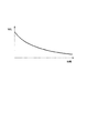
図11は、読み出し時に選択セルを流れるセル電流の時間推移を示した図である。選択したビット線BLを所定の電位に昇圧し、選択ゲート及び非選択WLをオンさせる。この時選択したワード線WLには判定を行いたいしきい値に対応した電位を与える。ベリファイ時の場合は、選択セルの満たさなければならない最低しきい値、即ちVverifyを与える場合もあるが、セルトランジスタ特性などから選択セルのしきい値を最も精度よく算出可能な電位に設定しても良い。選択セルのしきい値がVverifyに対して低い場合は、セル電流が流れてビット線の電位が低下していく。逆に選択セルのしきい値が高い場合、セル電流は流れずビット線電位は高いまま保持される。選択セルのしきい値がVverifyより低い場合でも、セルトランジスタの電流特性により、セル電流は選択セルのしきい値がVverifyに近づくに従って減少していく。ビット線電位の時間推移は、ビット線容量をセル電流で放電する過渡特性であり、セル電流が多いほど短時間でビット線電位は低下し、セル電流が少ないとビット線電位の低下は遅くなる。
【0046】
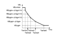
上記特性を利用したベリファイ方法を図12に示す。図12は、しきい値がVverify−ΔVpgm×4、Vverify−ΔVpgm×3、Vverify−ΔVpgm×2、Vverify−ΔVpgm×1、Vverify、の場合のセル電流の時間推移を示す。ビット線BLには、ビット線電位が所定の電位Vsenseを下回った時間(放電時間)を記憶する回路を接続する。上記しきい値の場合の放電時間をそれぞれ、Tsense1、Tsense2、Tsense3、Tsense4、Tsense5、とする。セル電流とビット線の放電特性とは一対一に対応するため、上記放電時間から選択セルのしきい値を算出することができる。そのため、放電時間を測定し、書き込み時のビット線電位に反映させることにより、しきい値の制御精度の劣化を最低限に抑えながら、高速な書き込み動作が可能となる。放電時間と選択セルのしきい値、書き込み時のビット線電位の組み合わせの一例を表1に示す。
【0047】
【表1】

【0048】
(第3実施形態)
別のベリファイ方法を利用した第3実施形態を図14に示す。図14は、読み出し時に選択セルを流れるセル電流の時間推移を示した図である。本第3実施形態が第2実施形態と異なるところは次の通りである。第2実施形態では、選択セルのしきい値を、ベリファイ動作においてビット線の電位が所定電位Vsenseに達する時間に基づき検知した。対して本第3実施形態では、選択セルのしきい値を、ベリファイ動作において所定時間Tsense経過時のビット線の電位に基づき検知する。図14は、しきい値がVverify−ΔVpgm×4、Vverify−ΔVpgm×3、Vverify−ΔVpgm×2、Vverify−ΔVpgm×1、Vverify、の場合のセル電流の時間推移を示す。ビット線BLには、所定時間Tsense経過時のビット線の電位を記憶する回路を接続する。上記しきい値の場合の放電後のビット線電位をそれぞれ、Vsense1、Vsense2、Vsense3、Vsense4、Vsense5、とする。セル電流とビット線の放電特性とは一対一に対応するため、上記放電後のビット線電位から選択セルのしきい値を算出することができる。そのため、放電後のビット線電位を測定し、書き込み時のビット線電位に反映させることにより、しきい値の制御精度の劣化を最低限に抑えながら、高速な書き込み動作が可能となる。放電後のビット線電位と選択セルのしきい値、書き込み時のビット線電位の組み合わせの一例を表2に示す。
【0049】
【表2】
【0050】
(第4実施形態)
第4実施形態として、上記第1〜第3実施形態に不揮発性半導体記憶装置を実現できる装置構成の一例を説明する。
【0051】
図16は、第4実施形態に係る不揮発性半導体記憶装置を示すブロック図である。
【0052】
図16に示すように、列方向(COLUMN)に沿って複数のビット線BL(BLk−1〜BLk+1)が形成されている。ビット線BLには、それぞれ不揮発性メモリセルトランジスタMCを含むメモリセルが接続されている。本例ではメモリセルの一例としてNAND型セル(NAND cell)を例示する。列方向と交差する行方向(ROW)に沿って並ぶセルトランジスタMCのゲート電極は、ワード線WL(WL1〜WL8)を介して各々接続されている。ビット線BLにはそれぞれ、データ読み出し時に、初期充電電位、例えば、読み出し電位(VBLread)を与える充電回路1、及びビット線駆動回路2がそれぞれ接続されている。充電回路1にはそれぞれ、例えば、読み出し制御信号Sreadが与えられる。充電回路1は制御信号Sreadに従ってビット線BLを初期充電電位に充電する。これにより、一つのワード線WLに接続された複数のセルトランジスタMCからデータが同時に読み出される。駆動回路2にはそれぞれ、検知回路(Detection CKT.)21、記憶回路(Storage CKT.)22、電位設定回路23が含まれている。検知回路21は、例えば、書き込みベリファイ動作においてセルトランジスタのしきい値を検知する。検知回路21の具体的一例はセンス回路である。記憶回路22は、検知回路21によって検知されたしきい値を記憶する。記憶回路22の具体的一例はデータラッチ回路である。記憶回路22は、第1実施形態に従えば2回以上行ったベリファイ読み出しの結果を記憶し、第2実施形態に従えばビット線BLの電位が所定電位Vsenseに達した時間を記憶し、第3実施形態に従えば所定時間Tsense経過時のビット線BLの電位を記憶する。このようにして記憶回路22は、選択セルのしきい値を記憶する。電位設定回路23は、記憶回路22に記憶されたしきい値に基づき、書き込みベリファイ動作に続く書き込み動作においてビット線BLの電位を、データ書き込みを禁止する書き込み禁止電位VBLinhibit、データ書き込みを行う書き込み電位VBLpgm、及びVBLinhibitとVBLpgmとの間の電位を持ち、書き込み量を抑制しながらデータ書き込みを行う書き込み抑制電位VBLpgm+ΔVpgmに設定する。不揮発性半導体記憶装置を、例えば、上記構成とすることにより、第1〜第3実施形態により説明した電位制御、ベリファイ動作を実現することができる。なお、図16には、ビット線BLk−1をVBLinhibit(V3)に、ビット線BLkをVBLpgm(V1)に、ビット線BLk+1をVBLpgm+ΔVpgm(V2)に設定している状態が示されている。
【0053】
(第5実施形態)
第5実施形態として、上記実施形態で説明した不揮発性半導体記憶装置を使用したアプリケーションの一例を説明する。
【0054】
図17は、この発明の第5実施形態に係るメモリカードの一例を示すブロック図である。
【0055】
図17に示すように、メモリカード97には、主記憶であるメモリチップ(Flash memory)92と、メモリチップ92を制御するコントローラチップ(controller)91とが含まれている。図17には、コントローラチップ91に含まれるいくつかの回路ブロックのうち、特に主記憶に関係する回路ブロックのみを説明する。
【0056】
主記憶に関係する回路ブロックとしては、例えば、シリアル/パラレル及びパラレル/シリアルインターフェース(Serial/Parallel and Parallel/Serial Interface)93、ページバッファ(Page Buffer)94、メモリインターフェース(Memory Interface)95が含まれる。
【0057】
インターフェース93は、データをメモリチップ92に書き込む際、例えば、シリアルな入力データ(Input data)を、パラレルな内部データに変換する。変換されたパラレルな内部データは、ページバッファ94に入力され、ここに蓄積される。蓄積された内部データは、メモリインターフェース95を介して、メモリチップ92に書き込まれる。
【0058】
また、データを、メモリカード97から読み出す際には、メモリチップル92から読み出したデータを、メモリインターフェース95を介して、ページバッファ94に入力し、ここに蓄積する。蓄積された内部データは、インターフェース93に入力され、ここでパラレルな内部データが、シリアルな出力データ(Output data)に変換されて、メモリカード97の外に出力される。
【0059】
このようなコントローラチップ91.及びメモリチップ92が、図17に示すように、カード型外装体(Card type Package)に収容、あるいは搭載、あるいは貼り付けられることで、メモリカードとして機能する。
【0060】
上記実施形態により説明した不揮発性半導体記憶装置は、メモリチップ92内のメモリ回路96に使用される。上記実施形態により説明した半導体記憶装置は、高速な書き込み動作を行いつつ、かつ高精度なしきい値分布幅制御を可能とする。従って、上記実施形態に係る半導体記憶装置を使用したメモリカード97によれば、メモリカード97と、これが接続される電子機器との間でのデータのやりとり、特に電子機器からのデータ書き込みを高速に行える、という利点を得ることができる。この利点故に、上記実施形態に係る半導体記憶装置を使用したメモリカード97は、高速なデータ書き込みを要求される電子機器、例えば、ビデオカメラ、デジタルスチルカメラ、パーソナルデジタルアシスタント等の記録メディアとして有用である。
【0061】
以上、上記実施形態に係る不揮発性半導体記憶装置によれば、書き込みベリファイの結果に従い、ビット線電位を個別に制御することにより、メモリセルのしきい値の制御精度を劣化させずに書き込み動作の高速化を図ることができる。
【0062】
また、この発明は、上記実施形態それぞれに限定されるものではなく、その実施にあたっては、発明の要旨を逸脱しない範囲で種々に変形することが可能である。例えば、上記実施形態ではメモリセルの一例としてNAND型セルを例示したが、この発明はNAND型セルを含むNAND型不揮発性半導体記憶装置に限って適用されるものではない。例えば、図18に示すように、AND型セルを含むAND型不揮発性半導体記憶装置にも適用することができるし、NAND型、AND型以外の不揮発性半導体記憶装置にも適用することができる。
【0063】
また、上記実施形態はそれぞれ、単独で実施することが可能であるが、適宜組み合わせて実施することも、もちろん可能である。
【0064】
また、上記実施形態には、種々の段階の発明が含まれており、各実施形態において開示した複数の構成要件の適宜な組み合わせにより、種々の段階の発明を抽出することも可能である。
【0065】
また、上記実施形態では、この発明を不揮発性半導体記憶装置に適用した例に基づき説明したが、上述したような不揮発性半導体記憶装置を内蔵した半導体集積回路装置、例えばプロセッサ、システムLSI等もまた、この発明の範疇である。
【0066】
【発明の効果】
この発明によれば、高速な書き込み動作を行いつつ、かつ高精度なしきい値分布幅制御を可能とする不揮発性半導体記憶装置及びそのデータ書き込み方法を提供できる。
【図面の簡単な説明】
【図1】図1は典型例に係る不揮発性半導体記憶装置を示すブロック図
【図2】図2は典型例に係る不揮発性半導体記憶装置が行うベリファイ動作を示す流れ図
【図3】図3は典型例に係る不揮発性半導体記憶装置の動作波形を示す動作波形図
【図4】図4はベリファイ前後のしきい値分布を示す図
【図5】図5A、図5B、図5C及び図5Dはこの発明の第1実施形態に係る不揮発性半導体記憶装置が行う電位制御の一例を示す図
【図6】図6はこの発明の第1実施形態に係る不揮発性半導体記憶装置が行うベリファイ動作の第1例を示す流れ図
【図7】図7はこの発明の第1実施形態に係る不揮発性半導体記憶装置の動作波形の第1例を示す動作波形図
【図8】図8はこの発明の第1実施形態に係る不揮発性半導体記憶装置が行うベリファイ動作の第2例を示す流れ図
【図9】図9はこの発明の第1実施形態に係る不揮発性半導体記憶装置の動作波形の第2例を示す動作波形図
【図10】図10はこの発明の第1実施形態の書き込みと典型的な書き込みとを対比して示す図
【図11】図11は読み出し時におけるビット線電位VBLと時間との関係を示す図
【図12】図12はこの発明の第2実施形態に係る不揮発性半導体記憶装置が行うベリファイ方法の一例を示す図
【図13】図13はこの発明の第2実施形態に係る不揮発性半導体記憶装置の書き込み時のビット線電位と放電時間との関係を示す図
【図14】図14はこの発明の第3実施形態に係る不揮発性半導体記憶装置が行うベリファイ方法の一例を示す図
【図15】図15はこの発明の第3実施形態に係る不揮発性半導体記憶装置の書き込み時のビット線電位と放電後のビット線電位との関係を示す図
【図16】図16はこの発明の第4実施形態に係る不揮発性半導体記憶装置を示すブロック図
【図17】図17はこの発明の第5実施形態に係るメモリカードの一例を示すブロック図
【図18】 図18はこの発明を適用できる不揮発性半導体記憶装置を示すブロック図
【符号の説明】
1…充電回路、2…ビット線駆動回路、21…検知回路、22…記憶回路、23…電位設定回路、91…コントローラチップ、92…メモリチップ、93…シリアル/パラレル及びパラレル/シリアルインターフェース、94…ページバッファ、95…メモリインターフェース、96…メモリ回路、97…メモリカード[0001]
BACKGROUND OF THE INVENTION
The present invention relates to a nonvolatile semiconductor memory device, and more particularly to data writing to a nonvolatile semiconductor memory device.
[0002]
[Prior art]
FIG. 1 shows an electrical connection diagram of a typical NAND type EEPROM. The NAND type EEPROM has a NAND type cell as a memory cell. The NANND type cell is composed of cell transistors arranged in series with their sources and drains connected to each other. Since the NAND type cell shares the source and drain between adjacent cell transistors, the contact between the bit line and the cell can be reduced and is suitable for high density. In addition, since the gates of a large number of cell transistors are driven simultaneously via the word line WL, data can be written / read at a high speed with respect to the large number of cell transistors.
[0003]
On the other hand, since the NAND type EEPROM reads data from the selected cell transistor, all the non-selected cell transistors in the NAND type cell must be turned on. Therefore, the threshold value of each cell transistor is controlled within a certain range. For example, if the threshold value is too low, separation from the non-written cell cannot be achieved, and conversely if it is too high, the cell cannot be turned on when it becomes a non-selected cell.
[0004]
As an example of controlling the threshold value of the cell transistor, FIG. 2 shows a write flow with a verify operation. After writing by applying a write gate potential (Vpgm) to the word line WL, reading is performed by applying a verify read gate potential (Vverify) to the word line WL. At this time, a sufficiently high read gate potential (Vread) is applied to a non-selected word line WL that has not been written, and a non-selected cell transistor is on. In this state, when the selected cell transistor is turned on, it is determined that the threshold value of the cell transistor is too low, that is, writing is insufficient, and Vpgm is increased by a predetermined amount (ΔVpgm) to perform the next writing. Do. This technique is called step-up writing, and is described in, for example,
[0005]
FIG. 3 shows an example of a time chart at the time of data writing in the NAND type EEPROM. The node names in the figure are the same as those in FIG. The bit line BLk in FIG. 1 is a write bit line, and the bit lines BLk + 1 and BLk−1 are write inhibit bit lines. At the time of writing, a predetermined gate potential (Vsg) is applied to the gate of the selection transistor SG1 on the bit line side. Next, a sufficiently low potential (VBLpgm) is applied to the bit line BLk to be written. Vsg is set to a potential that can sufficiently turn on the selection transistor SG1 with respect to VBLpgm. On the other hand, a sufficiently high potential (VBLinhibit) is applied to the bit lines BLk + 1 and BLk−1 for which writing is prohibited. VBLinhibit is set to a potential at which the selection transistor SG1 is sufficiently turned off. When VBLpgm is applied to the bit line, the select transistor SG1 is turned on, VBLpgm is transmitted to the cell transistor, and the channel potential of the cell transistor is sufficiently lowered to perform writing. On the other hand, when VBLinhibit is applied to the bit line BL, the selection transistor SG1 is turned off, the channel potential of the cell transistor is not lowered, and writing is not performed. This state is a write-inhibited state.
[0006]
At the time of initial writing, VBLpgm is applied to the bit line BLk connected to the cell transistor to be written, and VBLinhibit is applied to the bit lines BLk + 1 and BLk−1 connected to the cell transistor to be inhibited from writing. Vpgm is applied to the line WL. Subsequently, after the bit line BL is charged to a predetermined initial charging potential, Vverify is applied to the word line WL to perform verify read. When the cell transistor is turned on and the bit line BL is discharged, the writing is insufficient, so that writing is performed at the next writing. On the other hand, when the cell transistor is turned off and the bit line BL is not discharged, the writing is sufficient, so that the potential of the bit line BL is changed to VBLinhibit at the next writing to make the writing inhibited state. For the cell transistor that is determined to be insufficiently written, the potential of the word line WL is increased to Vpgm + ΔVpgm and additional writing is performed. In this way, the threshold value of the cell transistor is verified following writing, and based on the result, control is performed as to whether or not writing is performed at the next writing. These operations are repeated until the writing of all the cell transistors is completed while gradually increasing the potential of the word line WL. Thereby, the threshold value of the cell transistor is controlled within a desired range. That is, the lowest threshold value of the cell transistor is Vverify, and the threshold distribution width after the end of writing is determined by ΔVpgm. For this reason, if Vverify is set sufficiently high for non-write cells and Vverify + ΔVpgm is set sufficiently low for Vread, a desired threshold distribution can be obtained. FIG. 4 shows changes in threshold distribution during writing of the cell transistor.
[0007]
[Patent Document 1]
JP-A-7-169284
[0008]
[Patent Document 2]
US Pat. No. 5,555,204
[0009]
[Non-Patent Document 1]
G.J.Hemink, T.Tanaka, T.Endoh, S.Aritome, and R.Shirota
“Fast and accurate programming method for multi-level NAND flash EEPROM's”,
in SYMP. VLSI Technology Dig. Tech. Papers, June 1995, pp.129-130.
[0010]
[Problems to be solved by the invention]
In FIG. 4, if the variation in the write characteristics of the cell transistor is Wvt, the following conditions must be satisfied in order to obtain a desired threshold distribution.
[0011]
First write WL potential: The cell with the fastest write speed must not be written to Vverify + ΔVpgm or higher.
-Last write WL potential: The cell with the slowest write speed must be written to Vverify or higher.
During this time, the write WL potential needs to be increased by ΔVpgm. Therefore, assuming that the number of times of writing for writing all the cell transistors is Nloop, Nloop is expressed by the following equation.
[0012]
Nloop ≧ Wvt / ΔVpgm
As shown in this equation, the number of write times Nloop increases as the write characteristic variation Wvt of the cell transistor increases. The write characteristic variation Wvt is increasing with the miniaturization. For this reason, the situation that the writing speed decreases with the progress of miniaturization is becoming apparent.
[0013]
Further, the number of times of writing Nloop increases as ΔVpgm is decreased. When ΔVpgm is reduced, the threshold distribution width of the cell transistor is fine and can be controlled with high accuracy. This is a technique useful for, for example, lowering of the read potential Vread or multilevel memory. For example, the multilevel memory has a plurality of data orders below the read potential Vread. For this reason, in the multilevel memory, the threshold distribution width of the cell transistor must be controlled more finely and with higher accuracy than the binary memory. As described above, if the threshold distribution width of the cell transistor is fine and the control is to be performed with high accuracy, the number of times of writing Nloop increases and the writing speed decreases.
[0014]
The present invention has been made in view of the above circumstances, and an object of the present invention is to provide a nonvolatile semiconductor memory device and a data writing method thereof capable of high-speed threshold distribution width control while performing a high-speed writing operation. There is to do.
[0015]
[Means for Solving the Problems]
The nonvolatile semiconductor memory device according to the first aspect of the present invention includes:A plurality of wirings formed along a first direction, a memory cell including a nonvolatile memory cell transistor connected to each of the plurality of wirings via a selection transistor, and intersecting the first direction A word line for connecting the gate electrodes of the nonvolatile memory cell transistors arranged along a second direction; and a drive circuit connected to each of the plurality of wirings. A detection circuit for detecting a threshold value of the nonvolatile memory cell transistor, a storage circuit for storing the detected threshold value, and a write operation following the verify operation based on the threshold value stored in the storage circuit And a potential setting circuit for setting the potential of the wiring to three or more potentials, and the three or more potentials prohibit data writing. Including a write inhibit potential, a write potential for performing data write, and a write inhibit potential for performing data write while suppressing the write amount, and having a potential between the write inhibit potential and the write potential. During the write operation, the word line potential is stepped up from the word line potential at the time of data writing before the verify operation, and the step width of the word line potential is an integral multiple of the potential difference between the write potential and the write suppression potential. When the write potential and the write suppression potential are applied to the wiring and the stepped up word line potential is applied to the word line, the selection transistor is turned on, and the write inhibit potential is applied to the wiring. And the step-up word line potential is applied to the word line. When given, it is turned off the selection transistor.
[0016]
A data writing method of the nonvolatile semiconductor memory device according to the second aspect of the present invention includes:Write data to the non-volatile memory cell transistor, verify the threshold value of the non-volatile memory cell transistor to which the data has been written, and based on this result, if it is OK, set the potential of the bit line to inhibit data writing. If the potential is NG, the potential of the bit line is between the write potential for writing data according to the threshold value of the non-volatile memory cell transistor or between the write inhibit potential and the write potential. When data is additionally written to the nonvolatile memory cell transistor as one or more write suppression potentials for performing data writing while suppressing data, the word line potential is changed to a word at the time of data writing before verification. Step up from the line potential, the word line The step width of the power supply is an integral multiple of the potential difference between the write potential and the write suppression potential, the write potential and the write suppression potential are applied to the bit line, and the stepped up word line potential is the word line The bit line side select transistor is turned on, the write inhibit potential is applied to the bit line, and the stepped up word line potential is applied to the word line. The side select transistor is turned off.
[0017]
DETAILED DESCRIPTION OF THE INVENTION
Embodiments of the present invention will be described below with reference to the drawings. In the description, common parts are denoted by common reference symbols throughout the drawings.
[0018]
(First embodiment)
First, a write operation performed by the nonvolatile semiconductor memory device according to the first embodiment of the present invention will be described. 5A to 5D are diagrams illustrating examples of potential control performed in the write operation by the nonvolatile semiconductor memory device according to the first embodiment.
[0019]
FIG. 5A shows a case where a write potential (VBLpgm) is applied to the bit line BL, a write gate potential (Vpgm) is applied to the word line WL, and data is written to a selected cell transistor (hereinafter abbreviated as a selected cell). At this time, VBLpgm is set sufficiently lower than the gate potential (Vsg) of the select transistor SG1 on the bit line side. As a result, the select transistor SG1 is turned on, the channel potential of the selected cell is lowered to VBLpgm, and data is written to the selected cell up to a threshold value determined by Vpgm. Next, after the threshold value of the selected cell is verified by a verify operation, the potential of the word line WL is increased by a predetermined amount (ΔVpgm × 2), and the next write operation is started. In this next write operation, three states are selected as write states in the first embodiment.
[0020]
(I) Write status
A write potential VBLpgm is applied to the bit line BL, and a step-up write gate potential Vpgm + (ΔVpgm × 2) is applied to the word line WL. In this case, the selected cell is written in the same manner as the previous write, and the threshold value is increased by the increase of the word line potential, that is, ΔVpgm × 2. This state is shown in FIG. 5B.
[0021]
(Ii) Write suppression state
A write suppression potential VBLpgm + ΔVpgm is applied to the bit line BL, and a step-up write gate potential Vpgm + (ΔVpgm × 2) is applied to the word line WL. At this time, VBLpgm + ΔVpgm and Vsg are set so that the select transistor SG1 on the bit line side is sufficiently turned on. In this case, although writing is performed in the selected cell, a potential higher by ΔVpgm × 2−ΔVpgm = ΔVpgm than in the case of (i) is transferred to the channel of the selected cell. Therefore, ΔVpgm is canceled out of the increase ΔVpgm × 2 in the word line potential, and as a result, the threshold value of the selected cell is increased by ΔVpgm. This state is shown in FIG. 5C.
[0022]
(Iii) Write protected state
The write inhibit potential VBLinhibit is applied to the bit line BL, and the step-up write gate potential Vpgm + (ΔVpgm × 2) is applied to the word line WL. At this time, the selection transistor SG1 on the bit line side is turned off, the channel potential of the selected cell is not lowered, and writing is not performed. As a result, the threshold value of the selected cell does not increase. This state is shown in FIG. 5D.
[0023]
By selecting the three write states (i) to (iii) above, three results of “ΔVpgm × 2”, “ΔVpgm”, and “no increase” are obtained for the threshold value increase of the selected cell, respectively. You can expect.
[0024]
Next, a first example of the verify operation performed during the write operation will be described. FIG. 6 is a flowchart showing a first example of a verify operation performed by the nonvolatile semiconductor memory device according to the first embodiment.
[0025]
As shown in FIG. 6, first, data is written to the selected cell with the potential of the word line WL set to Vpgm (ST.1).
[0026]
Let Vverify be the lowest threshold that the selected cell must satisfy after the end of writing. In this case, first, data is read from the selected cell with the potential of the word line WL set to Vverify−ΔVpgm (ST.2: verify 1). As a result of reading, it is assumed that the selected cell is turned on and the potential of the bit line BL is lowered. A cell in which the potential of the bit line BL is lowered is set as group A (if NG). The threshold value of the group A cells is lower than Vverify−ΔVpgm.
[0027]
Next, data is read from the selected cell with the potential of the word line WL set to Vverify (ST.3: verify 2). At this time, a cell in which a current flows through the selected cell and the potential of the bit line BL is lowered, and a cell not included in the A group is set as the B group (if NG). The threshold value of the group B cells is Vverify−ΔVpgm or more and lower than Vverify. The remaining cells that are not included in either the A group or the B group are defined as a C group. The threshold value of the group C cells is equal to or higher than Vverify. Thereafter, the potential of the word line WL is increased by ΔVpgm × 2, and additional writing is performed (ST.4: additional writing). At the time of additional writing, the cells of the A group, the B group, and the C group are made to correspond to the states (i), (ii), and (iii), respectively. The state before and after the additional writing is summarized below.
[0028]
Group A (i) Write state:
-The threshold before additional writing is Vverify-ΔVpgm or less
・ Threshold increase during additional writing is ΔVpgm × 2.
-The threshold value after additional writing is Vverify + ΔVpgm or less
・ The threshold width that can be controlled by additional writing is ΔVpgm × 2.
Group B (ii) Write suppression state:
-The threshold before additional writing is Vverify-ΔVpgm or higher and lower than Vverify
・ Threshold increase during additional writing is ΔVpgm
-The threshold value after additional writing is Vverify or more and Vverify + ΔVpgm or less
-The threshold width that can be controlled by additional writing is ΔVpgm
Group C (iii) Write prohibited state:
-The threshold before additional writing is Vverify or higher
・ No increase in threshold during additional writing
-The threshold value after additional writing is maintained as it was before additional writing.
FIG. 7 shows an example of operation waveforms when the potential control during the write operation and the verify operation according to the first example are followed.
[0029]
Next, a second example of the verify operation will be described. FIG. 8 is a flowchart showing a second example of the verify operation performed by the nonvolatile semiconductor memory device according to the first embodiment. In the first example, after verifying the potential of the word line WL as Vverify−ΔVpgm, the potential of the word line WL is verified again as Vverify to determine the three write states (i) to (iii). The three write states (i) to (iii) can also be determined by verifying the potential of the word line WL as Vverify and then verifying the potential of the word line WL as Vverify−ΔVpgm again. The second example is an example of such determination.
[0030]
As shown in FIG. 8, first, data is written to the selected cell with the potential of the word line WL set to Vpgm (ST.1).
[0031]
After the writing is completed, data is read from the selected cell with the potential of the word line WL set to Vverify (ST.2: verify 1). As a result of reading, when the selected cell is turned off and the bit line BL is not discharged, it is determined that the threshold before additional writing is equal to or higher than Vverify (if OK), and the potential of the bit line BL is set to VBLinhibit. (ST.3: Write end). When the selected cell is turned on and the bit line BL is discharged, the setting of the potential of the bit line BL is left to the next read result (if NG).
[0032]
Next, data is read from the selected cell with the potential of the word line WL set to Vverify−ΔVpgm (ST.4: verify 2). As a result of reading, when the selected cell is turned off and the bit line BL is not discharged, it is determined that the threshold before additional writing is Vverify−ΔVpgm or more and lower than Vverify (if OK), and the bit line BL Is set to VBLpgm + ΔVpgm (ST.5: To write inhibited state). When the selected cell is turned on and the bit line BL is discharged, the threshold before additional writing is determined to be Vverify−ΔVpgm or less (if NG), and the potential of the bit line BL is set to VBLpgm (ST.6). : To write state. Thereafter, the potential of the word line WL is increased by ΔVpgm × 2, and additional writing is performed (ST.7: additional writing).
[0033]
FIG. 9 shows an example of operation waveforms when the potential control during the write operation and the verify operation according to the second example are followed.
[0034]
According to the nonvolatile semiconductor memory device according to the first embodiment, the following advantages can be obtained. The time required for writing is Tpgm, and the time required for verification is Tverify. These times include all the time required to actually generate an operation pulse, such as the time until the potential stabilizes, the time for restoring the node to which the potential is applied during the write operation, and the verify operation to the initial state. Shall be included. As shown in FIG. 10, when the typical example (Conventional) and the first embodiment (Proposed) are compared, in the first embodiment, one write operation (WRITE) is performed before the write potential is increased by ΔVpgm × 2. Less. For this reason, the time until the write potential is increased by ΔVpgm × 2 is Tpgm shorter than the typical example. Thereby, a high-speed write operation can be performed. Further, since the write suppression potential is set as the potential control at the time of writing, the controllable threshold width is not ΔVpgm × 2 but ΔVpgm. As a result, the threshold width can be controlled with high accuracy as in the typical example. In addition, since the potential control is performed individually for each bit line BL, the threshold distribution width control can be performed with high accuracy for each cell transistor.
[0035]
Further, the verify operation will be described in more detail. The verify operation is mainly composed of five times: a word line potential setting time, a bit line precharge time, a bit line discharge time, a bit line potential sense time, and a potential recovery time. In the operation waveform diagram of FIG. 9 according to the second example of the verify operation, the verify operation is two independent read operations. However, by appropriately setting the word line potential setting time and the bit line discharge time, after the bit line potential sensing time, only the word line potential is changed, and a series of readings for performing additional discharge from the bit line is performed. It is also possible. This is illustrated in FIG. 7 according to a first example of a verify operation. Therefore, the first example of the verify operation has an advantage that the bit line precharge time and the potential recovery time can be reduced by one time and the operation can be performed at a higher speed than the second example.
[0036]
In the write suppression state, the bit line potential can be further increased as long as the selection gate SG1 is sufficiently turned on. Therefore, for example, when it is desired to increase the word line potential by ΔVpgm × 3 at the time of additional writing, the following four can be selected as the writing state.
[0037]
(I) Write status
-Bit line potential = VBLpgm
(Ii)
-Bit line potential = VBLpgm + ΔVpgm
(Iii)
-Bit line potential = VBLpgm
(Iv) Write protected state
-Bit line potential = VBLinhibit
In order to determine the four write states (i) to (iV), for example, three potentials Vverify−ΔVpgm × 2, Vverify−ΔVpgm, and Vverify are applied to the word line WL. good. In this case, the time until the write potential is increased by ΔVpgm × 3 can be shortened by Tpgm × 2 with respect to the typical example while keeping the controlled threshold width equal to that of the typical example.
[0038]
Similarly, when it is desired to increase the word line potential by ΔVpgm × n at the time of additional writing, it is possible to select the next n + 1 as the writing state. However, n is an integer of 1 or more.
[0039]
(I) Write status
-Bit line potential = VBLpgm
(Ii)
-Bit line potential = VBLpgm + ΔVpgm
(Iii)
-Bit line potential = VBLpgm
...
(N) Write suppression state n-1
・ Bit line potential = VBLpgm + ΔVpgm × n−1
(N + 1) Write disabled state
-Bit line potential = VBLinhibit
In order to determine the n + 1 write states (i) to (n + 1), for example, the potential applied to the word line WL is Vverify−ΔVpgm × (n−1), Vverify−ΔVpgm × (n−2),. Vverify−ΔVpgm × 2, Vverify−ΔVpgm, and Vverify are set to n, and reading may be performed a total of n times. In this case, it is possible to shorten the time until the write potential is increased by ΔVpgm × n by Tpgm × (n−1) with respect to the typical example while keeping the controlled threshold width equal to the typical example. .
[0040]
As described above, according to the first embodiment, in the memory in which a discrete potential can be set to the bit line at the time of writing, the verify read appropriately set for each is performed, and the bit line potential at the time of the next writing is determined based on the result. Thus, it is possible to perform a high-speed write operation while minimizing the deterioration of the threshold control accuracy. Alternatively, it is possible to improve the threshold control accuracy while minimizing the deterioration of the writing speed.
[0041]
The upper limit of the bit line potential at the time of writing in the first embodiment is given on the condition that the selection gate SG1 is sufficiently turned on. Therefore, when ΔVpgm is small, for example, when high-precision threshold control is required as in a multi-level memory, it is possible to obtain the advantage better.
[0042]
In the first embodiment, the minimum amount of word line potential fluctuation at the time of verification is described as being the same as the minimum amount of bit line potential fluctuation at the time of writing. However, an appropriate calibration method is defined, and the bit line potential at the time of writing is defined. As long as there is a one-to-one correspondence with the threshold value that is suppressed by the rise of the threshold value, the threshold value control according to the present invention can be realized even if a verification method different from the above-described reading method is selected. It is clear.
[0043]
For example, the threshold value of the selected cell changes the potential applied to the gate electrode of the selected cell in the verify operation, the initial charge potential applied to the bit line in the verify operation, the determination reference potential for determining the potential of the bit line, and the bit It is possible to detect by changing at least one of the determination reference times for determining the line potential and performing verify reading twice or more. It is also possible to combine these verify methods in various ways.
[0044]
In addition, for example, when a negative word line potential is required as a verify potential, a method of performing reading by applying a positive bias to a substrate on which a cell transistor exists or a common source line is generally used. It is also possible to use a combination of a plurality of verification methods depending on conditions such as potential.
[0045]
(Second Embodiment)
FIG. 11 is a diagram showing a time transition of the cell current flowing through the selected cell at the time of reading. The selected bit line BL is boosted to a predetermined potential, and the selection gate and the non-selected WL are turned on. At this time, a potential corresponding to a threshold value to be determined is applied to the selected word line WL. In the case of verify, there is a case where the minimum threshold value that must be satisfied by the selected cell, that is, Vverify may be given. Also good. When the threshold value of the selected cell is lower than Vverify, the cell current flows and the potential of the bit line decreases. Conversely, when the threshold value of the selected cell is high, the cell current does not flow and the bit line potential is kept high. Even when the threshold value of the selected cell is lower than Vverify, the cell current decreases as the threshold value of the selected cell approaches Vverify due to the current characteristics of the cell transistor. The time transition of the bit line potential is a transient characteristic in which the bit line capacitance is discharged by the cell current. The higher the cell current, the shorter the bit line potential decreases, and the lower the cell current, the slower the bit line potential decreases. .
[0046]
FIG. 12 shows a verify method using the above characteristics. FIG. 12 shows the time transition of the cell current when the threshold values are Vverify−ΔVpgm × 4, Vverify−ΔVpgm × 3, Vverify−ΔVpgm × 2, Vverify−ΔVpgm × 1, and Vverify. A circuit for storing a time (discharge time) when the bit line potential is lower than a predetermined potential Vsense is connected to the bit line BL. The discharge times for the above threshold values are Tsense1, Tsense2, Tsense3, Tsense4, and Tsense5, respectively. Since the cell current and the discharge characteristic of the bit line have a one-to-one correspondence, the threshold value of the selected cell can be calculated from the discharge time. Therefore, by measuring the discharge time and reflecting it in the bit line potential at the time of writing, it is possible to perform a high-speed writing operation while minimizing the deterioration of the threshold control accuracy. Table 1 shows an example of combinations of the discharge time, the threshold value of the selected cell, and the bit line potential at the time of writing.
[0047]
[Table 1]
[0048]
(Third embodiment)
FIG. 14 shows a third embodiment using another verify method. FIG. 14 is a diagram showing a time transition of the cell current flowing through the selected cell at the time of reading. The third embodiment is different from the second embodiment as follows. In the second embodiment, the threshold value of the selected cell is detected based on the time when the bit line potential reaches the predetermined potential Vsense in the verify operation. In contrast, in the third embodiment, the threshold value of the selected cell is detected based on the potential of the bit line when the predetermined time Tsense has elapsed in the verify operation. FIG. 14 shows the time transition of the cell current when the threshold values are Vverify−ΔVpgm × 4, Vverify−ΔVpgm × 3, Vverify−ΔVpgm × 2, Vverify−ΔVpgm × 1, and Vverify. A circuit for storing the potential of the bit line when the predetermined time Tsense has elapsed is connected to the bit line BL. The bit line potentials after discharge in the case of the above threshold are Vsense1, Vsense2, Vsense3, Vsense4, and Vsense5, respectively. Since the cell current and the discharge characteristic of the bit line have a one-to-one correspondence, the threshold value of the selected cell can be calculated from the bit line potential after the discharge. Therefore, by measuring the bit line potential after discharge and reflecting it in the bit line potential at the time of writing, it is possible to perform a high-speed writing operation while minimizing deterioration in threshold control accuracy. Table 2 shows an example of combinations of the bit line potential after discharge, the threshold value of the selected cell, and the bit line potential at the time of writing.
[0049]
[Table 2]
[0050]
(Fourth embodiment)
As a fourth embodiment, an example of a device configuration capable of realizing a nonvolatile semiconductor memory device in the first to third embodiments will be described.
[0051]
FIG. 16 is a block diagram showing a nonvolatile semiconductor memory device according to the fourth embodiment.
[0052]
As shown in FIG. 16, a plurality of bit lines BL (BLk−1 to BLk + 1) are formed along the column direction (COLUMN). Each bit line BL is connected to a memory cell including a nonvolatile memory cell transistor MC. In this example, a NAND cell is illustrated as an example of the memory cell. The gate electrodes of the cell transistors MC arranged along the row direction (ROW) intersecting the column direction are connected to each other via word lines WL (WL1 to WL8). Each bit line BL is connected to a
[0053]
(Fifth embodiment)
As a fifth embodiment, an example of an application using the nonvolatile semiconductor memory device described in the above embodiment will be described.
[0054]
FIG. 17 is a block diagram showing an example of a memory card according to the fifth embodiment of the present invention.
[0055]
As shown in FIG. 17, the
[0056]
Circuit blocks related to the main memory include, for example, a serial / parallel and parallel / serial interface (Serial / Parallel and Parallel / Serial Interface) 93, a page buffer (Page Buffer) 94, and a memory interface (Memory Interface) 95. .
[0057]
When writing data to the
[0058]
When data is read from the
[0059]
Such a
[0060]
The nonvolatile semiconductor memory device described in the above embodiment is used for the
[0061]
As described above, according to the nonvolatile semiconductor memory device according to the above embodiment, the bit line potential is individually controlled according to the result of the write verification, so that the write operation can be performed without degrading the control accuracy of the threshold value of the memory cell. The speed can be increased.
[0062]
Further, the present invention is not limited to each of the embodiments described above, and various modifications can be made without departing from the spirit of the invention. For example, although the NAND type cell is illustrated as an example of the memory cell in the above embodiment, the present invention is not limited to the NAND type nonvolatile semiconductor memory device including the NAND type cell. For example, as shown in FIG. 18, the present invention can be applied to an AND type nonvolatile semiconductor memory device including an AND type cell, and can also be applied to nonvolatile semiconductor memory devices other than NAND type and AND type.
[0063]
In addition, each of the above embodiments can be carried out independently, but it is of course possible to carry out a combination as appropriate.
[0064]
The above embodiments include inventions at various stages, and the inventions at various stages can be extracted by appropriately combining a plurality of constituent elements disclosed in each embodiment.
[0065]
In the above embodiment, the present invention has been described based on an example in which the present invention is applied to a nonvolatile semiconductor memory device. However, a semiconductor integrated circuit device incorporating a nonvolatile semiconductor memory device as described above, for example, a processor, a system LSI, etc. This is the category of the present invention.
[0066]
【The invention's effect】
According to the present invention, it is possible to provide a nonvolatile semiconductor memory device and a data writing method thereof capable of performing a high-precision threshold distribution width control while performing a high-speed writing operation.
[Brief description of the drawings]
FIG. 1 is a block diagram showing a nonvolatile semiconductor memory device according to a typical example.
FIG. 2 is a flowchart showing a verify operation performed by a nonvolatile semiconductor memory device according to a typical example;
FIG. 3 is an operation waveform diagram showing operation waveforms of a nonvolatile semiconductor memory device according to a typical example;
FIG. 4 is a diagram showing threshold distributions before and after verification;
5A, 5B, 5C, and 5D are diagrams showing an example of potential control performed by the nonvolatile semiconductor memory device according to the first embodiment of the present invention. FIG.
FIG. 6 is a flowchart showing a first example of a verify operation performed by the nonvolatile semiconductor memory device according to the first embodiment of the invention;
FIG. 7 is an operation waveform diagram showing a first example of operation waveforms of the nonvolatile semiconductor memory device according to the first embodiment of the present invention;
FIG. 8 is a flowchart showing a second example of a verify operation performed by the nonvolatile semiconductor memory device according to the first embodiment of the invention;
FIG. 9 is an operation waveform diagram showing a second example of operation waveforms of the nonvolatile semiconductor memory device according to the first embodiment of the invention;
FIG. 10 is a diagram showing a comparison between writing and typical writing according to the first embodiment of the present invention;
FIG. 11 is a diagram showing a relationship between a bit line potential VBL and time at the time of reading;
FIG. 12 is a diagram showing an example of a verify method performed by the nonvolatile semiconductor memory device according to the second embodiment of the present invention;
FIG. 13 is a view showing a relationship between a bit line potential and a discharge time at the time of writing in the nonvolatile semiconductor memory device according to the second embodiment of the present invention;
FIG. 14 is a diagram showing an example of a verify method performed by the nonvolatile semiconductor memory device according to the third embodiment of the invention.
FIG. 15 is a diagram showing a relationship between a bit line potential at the time of writing and a bit line potential after discharge in the nonvolatile semiconductor memory device according to the third embodiment of the present invention;
FIG. 16 is a block diagram showing a nonvolatile semiconductor memory device according to a fourth embodiment of the invention.
FIG. 17 is a block diagram showing an example of a memory card according to a fifth embodiment of the present invention.
FIG. 18 is a block diagram showing a nonvolatile semiconductor memory device to which the present invention can be applied.
[Explanation of symbols]
DESCRIPTION OF
Claims (16)
前記複数の配線それぞれに、選択トランジスタを介して接続された、不揮発性メモリセルトランジスタを含むメモリセルと、
前記第1の方向と交差する第2の方向に沿って並ぶ前記不揮発性メモリセルトランジスタのゲート電極を各々接続するワード線と、
前記複数の配線それぞれに接続された駆動回路とを具備し、
前記駆動回路は、ベリファイ動作において前記不揮発性メモリセルトランジスタのしきい値を検知する検知回路と、
前記検知されたしきい値を記憶する記憶回路と、
前記記憶回路に記憶されたしきい値に基づき、前記ベリファイ動作に続く書き込み動作において前記配線の電位を3つ以上の電位に設定する電位設定回路と
を具備し、
前記3つ以上の電位は、データ書き込みを禁止する書き込み禁止電位、データ書き込みを行う書き込み電位、及び前記書き込み禁止電位と前記書き込み電位との間の電位を持ち、書き込み量を抑制しながらデータ書き込みを行う書き込み抑制電位を含み、
前記ベリファイ動作に続く書き込み動作の際、ワード線電位を前記ベリファイ動作前のデータ書き込み時のワード線電位よりもステップアップし、
前記ワード線電位のステップ幅は、前記書き込み電位と前記書き込み抑制電位との電位差の整数倍であり、
前記書き込み電位及び前記書き込み抑制電位が前記配線に与えられ、前記ステップアップされたワード線電位がワード線に与えられた時、前記選択トランジスタをオン状態とし、前記書き込み禁止電位が前記配線に与えられ、前記ステップアップされたワード線電位が前記ワード線に与えられたとき、前記選択トランジスタをオフ状態とすることを特徴とする不揮発性半導体記憶装置。A plurality of wirings formed along the first direction;
A memory cell including a nonvolatile memory cell transistor connected to each of the plurality of wirings via a selection transistor ;
Word lines respectively connecting gate electrodes of the non-volatile memory cell transistors arranged along a second direction intersecting the first direction;
A drive circuit connected to each of the plurality of wirings;
The drive circuit includes a detection circuit that detects a threshold value of the nonvolatile memory cell transistor in a verify operation;
A storage circuit for storing the detected threshold value;
A potential setting circuit that sets the potential of the wiring to three or more potentials in a write operation subsequent to the verify operation based on the threshold value stored in the storage circuit ;
The three or more potentials include a write inhibit potential for prohibiting data write, a write potential for performing data write, and a potential between the write inhibit potential and the write potential, and data writing can be performed while suppressing the write amount. Including write suppression potential to perform,
During the write operation following the verify operation, the word line potential is stepped up from the word line potential at the time of data writing before the verify operation,
The step width of the word line potential is an integral multiple of the potential difference between the write potential and the write suppression potential,
When the write potential and the write suppression potential are applied to the wiring and the stepped up word line potential is applied to the word line, the selection transistor is turned on, and the write inhibit potential is applied to the wiring. The nonvolatile semiconductor memory device is characterized in that when the stepped up word line potential is applied to the word line, the selection transistor is turned off .
前記ベリファイ動作において
前記不揮発性メモリセルトランジスタのゲート電極に与える電位、
前記配線に与える初期充電電位、
前記配線の電位を判定する判定基準電位、及び
前記配線の電位を判定する判定基準時間、
の少なくともいずれか1つを変更し、前記ベリファイ読み出しを2回以上行って検知されることを特徴とする請求項1に記載の不揮発性半導体記憶装置。The threshold value of the nonvolatile memory cell transistor is:
A potential applied to a gate electrode of the nonvolatile memory cell transistor in the verify operation;
Initial charging potential applied to the wiring,
A determination reference potential for determining the potential of the wiring, and a determination reference time for determining the potential of the wiring,
2. The nonvolatile semiconductor memory device according to claim 1 , wherein the detection is performed by changing at least one of the read and performing the verify read twice or more.
前記ベリファイ動作において前記配線の電位が所定電位に達する時間に基づき検知されることを特徴とする請求項1に記載の不揮発性半導体記憶装置。The threshold value of the nonvolatile memory cell transistor is:
2. The nonvolatile semiconductor memory device according to claim 1 , wherein in the verify operation, detection is made based on a time during which the potential of the wiring reaches a predetermined potential.
前記ベリファイ動作において所定時間経過時の前記配線の電位に基づき検知されることを特徴とする請求項1に記載の不揮発性半導体記憶装置。The threshold value of the nonvolatile memory cell transistor is:
The nonvolatile semiconductor memory device according to claim 1 , wherein detection is performed based on a potential of the wiring when a predetermined time has elapsed in the verify operation.
前記データが書き込まれた不揮発性メモリセルトランジスタのしきい値をベリファイし、この結果に基づき、
OKならばビット線の電位を、データ書き込みを禁止する書き込み禁止電位とし、
NGならば前記ビット線の電位を、前記不揮発性メモリセルトランジスタのしきい値に応じてデータ書き込みを行う書き込み電位、あるいは前記書き込み禁止電位と前記書き込み電位との間にあり、書き込み量を抑制しながらデータ書き込みを行う1つ以上の書き込み抑制電位として前記不揮発性メモリセルトランジスタにデータを追加書き込みし、
前記データを追加書き込みする際、ワード線電位を前記ベリファイ前のデータ書き込み時のワード線電位よりもステップアップし、
前記ワード線電位のステップ幅は、前記書き込み電位と前記書き込み抑制電位との電位差の整数倍であり、
前記書き込み電位及び前記書き込み抑制電位が前記ビット線に与えられ、前記ステップアップされたワード線電位がワード線に与えられた時、ビット線側の選択トランジスタをオン状態とし、前記書き込み禁止電位が前記ビット線に与えられ、前記ステップアップされたワード線電位が前記ワード線に与えられたとき、前記ビット線側の選択トランジスタをオフ状態とすることを特徴とする不揮発性半導体記憶装置のデータ書き込み方法。Write data to the non-volatile memory cell transistor,
The threshold value of the nonvolatile memory cell transistor in which the data is written is verified, and based on the result,
If OK, the bit line potential is set to a write inhibit potential for inhibiting data writing,
In the case of NG, the potential of the bit line is between the write potential for writing data according to the threshold value of the nonvolatile memory cell transistor, or between the write inhibit potential and the write potential, and the write amount is suppressed. While writing data to the nonvolatile memory cell transistor as one or more write suppression potentials for writing data ,
When the data is additionally written, the word line potential is stepped up from the word line potential at the time of data writing before the verification,
The step width of the word line potential is an integral multiple of the potential difference between the write potential and the write suppression potential,
When the write potential and the write suppression potential are applied to the bit line, and the stepped up word line potential is applied to the word line, the selection transistor on the bit line side is turned on, and the write inhibit potential is A data writing method for a nonvolatile semiconductor memory device , wherein a selection transistor on the bit line side is turned off when the word line potential applied to the bit line and the stepped up word line is applied to the word line. .
ワード線電位をベリファイ電位と異なる電位としてデータを読み出し判定されることを特徴とする請求項12に記載の不揮発性半導体記憶装置のデータ書き込み方法。The threshold value of the nonvolatile memory cell transistor is:
13. The method of writing data in a nonvolatile semiconductor memory device according to claim 12 , wherein data is read and determined with the word line potential different from the verify potential.
Priority Applications (3)
| Application Number | Priority Date | Filing Date | Title |
|---|---|---|---|
| JP2002347799A JP3889699B2 (en) | 2002-11-29 | 2002-11-29 | Nonvolatile semiconductor memory device and data writing method thereof |
| US10/700,508 US6807104B2 (en) | 2002-11-29 | 2003-11-05 | Nonvolatile semiconductor memory device and data program method thereof |
| KR1020030085434A KR100554998B1 (en) | 2002-11-29 | 2003-11-28 | Nonvolatile semiconductor memory device and data writing method thereof |
Applications Claiming Priority (1)
| Application Number | Priority Date | Filing Date | Title |
|---|---|---|---|
| JP2002347799A JP3889699B2 (en) | 2002-11-29 | 2002-11-29 | Nonvolatile semiconductor memory device and data writing method thereof |
Publications (2)
| Publication Number | Publication Date |
|---|---|
| JP2004185659A JP2004185659A (en) | 2004-07-02 |
| JP3889699B2 true JP3889699B2 (en) | 2007-03-07 |
Family
ID=32708051
Family Applications (1)
| Application Number | Title | Priority Date | Filing Date |
|---|---|---|---|
| JP2002347799A Expired - Fee Related JP3889699B2 (en) | 2002-11-29 | 2002-11-29 | Nonvolatile semiconductor memory device and data writing method thereof |
Country Status (3)
| Country | Link |
|---|---|
| US (1) | US6807104B2 (en) |
| JP (1) | JP3889699B2 (en) |
| KR (1) | KR100554998B1 (en) |
Families Citing this family (33)
| Publication number | Priority date | Publication date | Assignee | Title |
|---|---|---|---|---|
| US7064981B2 (en) * | 2004-08-04 | 2006-06-20 | Micron Technology, Inc. | NAND string wordline delay reduction |
| ITRM20050310A1 (en) * | 2005-06-15 | 2006-12-16 | Micron Technology Inc | SLOW CONVERGENCE IN SELECTIVE PROGRAMMING IN A FLASH MEMORY DEVICE. |
| KR100648290B1 (en) * | 2005-07-26 | 2006-11-23 | 삼성전자주식회사 | Nonvolatile memory device and its programming method which can improve program speed |
| KR100719372B1 (en) * | 2005-08-10 | 2007-05-17 | 삼성전자주식회사 | NOR flash memory device and its program method |
| JP4405456B2 (en) * | 2005-10-27 | 2010-01-27 | 株式会社東芝 | Nonvolatile semiconductor memory device |
| US7352629B2 (en) * | 2005-12-29 | 2008-04-01 | Sandisk Corporation | Systems for continued verification in non-volatile memory write operations |
| US7307887B2 (en) * | 2005-12-29 | 2007-12-11 | Sandisk Corporation | Continued verification in non-volatile memory write operations |
| JP4177847B2 (en) * | 2006-01-06 | 2008-11-05 | 株式会社東芝 | Nonvolatile semiconductor memory device |
| JP4157562B2 (en) * | 2006-01-31 | 2008-10-01 | 株式会社東芝 | Semiconductor integrated circuit device |
| US7397703B2 (en) * | 2006-03-21 | 2008-07-08 | Freescale Semiconductor, Inc. | Non-volatile memory with controlled program/erase |
| US7502254B2 (en) * | 2006-04-11 | 2009-03-10 | Sandisk Il Ltd | Method for generating soft bits in flash memories |
| JP5426069B2 (en) * | 2006-08-31 | 2014-02-26 | 富士通セミコンダクター株式会社 | Semiconductor device and manufacturing method thereof |
| JP4997882B2 (en) * | 2006-09-05 | 2012-08-08 | ソニー株式会社 | Nonvolatile semiconductor memory device and writing method thereof |
| US20080158986A1 (en) * | 2006-12-29 | 2008-07-03 | Daniel Elmhurst | Flash memory and associated methods |
| JP4936914B2 (en) * | 2007-01-23 | 2012-05-23 | 株式会社東芝 | Semiconductor memory device |
| US7599224B2 (en) * | 2007-07-03 | 2009-10-06 | Sandisk Corporation | Systems for coarse/fine program verification in non-volatile memory using different reference levels for improved sensing |
| US7508715B2 (en) * | 2007-07-03 | 2009-03-24 | Sandisk Corporation | Coarse/fine program verification in non-volatile memory using different reference levels for improved sensing |
| US7619933B2 (en) * | 2007-10-05 | 2009-11-17 | Micron Technology, Inc. | Reducing effects of program disturb in a memory device |
| US8355278B2 (en) | 2007-10-05 | 2013-01-15 | Micron Technology, Inc. | Reducing effects of program disturb in a memory device |
| EP2274746A1 (en) * | 2008-04-29 | 2011-01-19 | SanDisk IL Ltd. | Non-volatile multilevel memory with adaptive setting of reference voltage levels for program, verify and read |
| US8102187B2 (en) * | 2008-05-02 | 2012-01-24 | Texas Instruments Incorporated | Localized calibration of programmable digital logic cells |
| JP2010009733A (en) * | 2008-06-30 | 2010-01-14 | Toshiba Corp | Nonvolatile semiconductor memory device |
| JP2010045175A (en) * | 2008-08-12 | 2010-02-25 | Toshiba Corp | Non-volatile semiconductor memory device |
| JP5193830B2 (en) | 2008-12-03 | 2013-05-08 | 株式会社東芝 | Nonvolatile semiconductor memory |
| WO2010089815A1 (en) * | 2009-02-06 | 2010-08-12 | パナソニック株式会社 | Nonvolatile semiconductor memory |
| KR20110131648A (en) * | 2010-05-31 | 2011-12-07 | 삼성전자주식회사 | Non-volatile memory device, memory system and memory card including it and program method thereof |
| JP5153895B2 (en) * | 2011-01-12 | 2013-02-27 | ルネサスエレクトロニクス株式会社 | Writing method for nonvolatile semiconductor memory device |
| KR101278103B1 (en) * | 2011-09-26 | 2013-06-24 | 에스케이하이닉스 주식회사 | Nonvolatile memory device and programming method thereof |
| KR20170073980A (en) * | 2015-12-21 | 2017-06-29 | 에스케이하이닉스 주식회사 | Semiconductor memory device and operating method thereof |
| TWI665677B (en) * | 2018-06-08 | 2019-07-11 | 旺宏電子股份有限公司 | Method for performing program inhibit operation with cell disturbance alleviation, memory device and controller |
| US20190378582A1 (en) * | 2018-06-08 | 2019-12-12 | Macronix International Co., Ltd. | Method for performing program inhibit operation with cell disturbance alleviation, memory device and controller |
| JP2021039807A (en) | 2019-09-03 | 2021-03-11 | キオクシア株式会社 | Semiconductor storage device |
| US11842775B2 (en) * | 2021-10-21 | 2023-12-12 | Sandisk Technologies Llc | Systems and methods for dynamically sensing a memory block |
Family Cites Families (8)
| Publication number | Priority date | Publication date | Assignee | Title |
|---|---|---|---|---|
| JP3626221B2 (en) | 1993-12-13 | 2005-03-02 | 株式会社東芝 | Nonvolatile semiconductor memory device |
| US5555204A (en) | 1993-06-29 | 1996-09-10 | Kabushiki Kaisha Toshiba | Non-volatile semiconductor memory device |
| JP3730272B2 (en) | 1994-09-17 | 2005-12-21 | 株式会社東芝 | Nonvolatile semiconductor memory device |
| US5903495A (en) * | 1996-03-18 | 1999-05-11 | Kabushiki Kaisha Toshiba | Semiconductor device and memory system |
| US6026014A (en) * | 1996-12-20 | 2000-02-15 | Hitachi, Ltd. | Nonvolatile semiconductor memory and read method |
| KR100323554B1 (en) | 1997-05-14 | 2002-03-08 | 니시무로 타이죠 | Non-volatile semiconductor memory |
| US6314026B1 (en) | 1999-02-08 | 2001-11-06 | Kabushiki Kaisha Toshiba | Nonvolatile semiconductor device using local self boost technique |
| JP2001067884A (en) * | 1999-08-31 | 2001-03-16 | Hitachi Ltd | Nonvolatile semiconductor memory device |
-
2002
- 2002-11-29 JP JP2002347799A patent/JP3889699B2/en not_active Expired - Fee Related
-
2003
- 2003-11-05 US US10/700,508 patent/US6807104B2/en not_active Expired - Lifetime
- 2003-11-28 KR KR1020030085434A patent/KR100554998B1/en not_active Expired - Fee Related
Also Published As
| Publication number | Publication date |
|---|---|
| JP2004185659A (en) | 2004-07-02 |
| KR100554998B1 (en) | 2006-02-24 |
| US20040141377A1 (en) | 2004-07-22 |
| US6807104B2 (en) | 2004-10-19 |
| KR20040047721A (en) | 2004-06-05 |
Similar Documents
| Publication | Publication Date | Title |
|---|---|---|
| JP3889699B2 (en) | Nonvolatile semiconductor memory device and data writing method thereof | |
| JP4855271B2 (en) | A method for reading a NAND memory that compensates for coupling between storage elements. | |
| US7177199B2 (en) | Behavior based programming of non-volatile memory | |
| JP4936914B2 (en) | Semiconductor memory device | |
| JP3631463B2 (en) | Nonvolatile semiconductor memory device | |
| KR101119371B1 (en) | Semiconductor memory apparatus and a method of operating thereof | |
| US7259987B2 (en) | Systems for variable programming of non-volatile memory | |
| JP3810985B2 (en) | Nonvolatile semiconductor memory | |
| US6418058B1 (en) | Nonvolatile semiconductor memory device | |
| US20090323432A1 (en) | Nonvolatile semiconductor memory device | |
| JP3977799B2 (en) | Nonvolatile semiconductor memory device | |
| CN112927741B (en) | Method of programming and verifying a memory device and related memory device | |
| JP2011008857A (en) | Nonvolatile semiconductor memory device and writing method thereof | |
| JP2004185688A (en) | Nonvolatile semiconductor memory device and erase verify method therefor | |
| US7724576B2 (en) | Soft programming method of non-volatile memory device | |
| US8422301B2 (en) | Nonvolatile semiconductor memory device and operating method thereof | |
| CN114783488B (en) | Page buffer, programming method, memory device and system | |
| JP2007102865A (en) | Semiconductor integrated circuit device | |
| JP2007305204A (en) | Nonvolatile semiconductor memory device | |
| JP2007102848A (en) | Semiconductor integrated circuit device | |
| JP2000090679A (en) | Nonvolatile semiconductor memory device |
Legal Events
| Date | Code | Title | Description |
|---|---|---|---|
| A977 | Report on retrieval |
Free format text: JAPANESE INTERMEDIATE CODE: A971007 Effective date: 20060811 |
|
| A131 | Notification of reasons for refusal |
Free format text: JAPANESE INTERMEDIATE CODE: A131 Effective date: 20060829 |
|
| A521 | Written amendment |
Free format text: JAPANESE INTERMEDIATE CODE: A523 Effective date: 20061030 |
|
| TRDD | Decision of grant or rejection written | ||
| A01 | Written decision to grant a patent or to grant a registration (utility model) |
Free format text: JAPANESE INTERMEDIATE CODE: A01 Effective date: 20061128 |
|
| A61 | First payment of annual fees (during grant procedure) |
Free format text: JAPANESE INTERMEDIATE CODE: A61 Effective date: 20061130 |
|
| FPAY | Renewal fee payment (event date is renewal date of database) |
Free format text: PAYMENT UNTIL: 20091208 Year of fee payment: 3 |
|
| FPAY | Renewal fee payment (event date is renewal date of database) |
Free format text: PAYMENT UNTIL: 20101208 Year of fee payment: 4 |
|
| FPAY | Renewal fee payment (event date is renewal date of database) |
Free format text: PAYMENT UNTIL: 20111208 Year of fee payment: 5 |
|
| FPAY | Renewal fee payment (event date is renewal date of database) |
Free format text: PAYMENT UNTIL: 20121208 Year of fee payment: 6 |
|
| LAPS | Cancellation because of no payment of annual fees |