JP3806826B2 - Driving circuit for vibrating mirror type scanning device - Google Patents
Driving circuit for vibrating mirror type scanning device Download PDFInfo
- Publication number
- JP3806826B2 JP3806826B2 JP04687697A JP4687697A JP3806826B2 JP 3806826 B2 JP3806826 B2 JP 3806826B2 JP 04687697 A JP04687697 A JP 04687697A JP 4687697 A JP4687697 A JP 4687697A JP 3806826 B2 JP3806826 B2 JP 3806826B2
- Authority
- JP
- Japan
- Prior art keywords
- pulse
- voltage
- period
- pulse train
- oscillation
- Prior art date
- Legal status (The legal status is an assumption and is not a legal conclusion. Google has not performed a legal analysis and makes no representation as to the accuracy of the status listed.)
- Expired - Lifetime
Links
- 230000010355 oscillation Effects 0.000 claims abstract description 104
- 230000005284 excitation Effects 0.000 claims abstract description 83
- 238000006243 chemical reaction Methods 0.000 claims description 116
- 230000005279 excitation period Effects 0.000 claims description 24
- 238000005070 sampling Methods 0.000 claims description 24
- 230000002441 reversible effect Effects 0.000 claims description 19
- 230000000630 rising effect Effects 0.000 claims description 14
- 238000001514 detection method Methods 0.000 abstract description 5
- 239000003990 capacitor Substances 0.000 description 21
- 238000010586 diagram Methods 0.000 description 19
- 238000000034 method Methods 0.000 description 9
- 230000008859 change Effects 0.000 description 7
- 230000003287 optical effect Effects 0.000 description 4
- 239000013641 positive control Substances 0.000 description 3
- 230000003321 amplification Effects 0.000 description 2
- 230000005540 biological transmission Effects 0.000 description 2
- 238000007599 discharging Methods 0.000 description 2
- 230000000694 effects Effects 0.000 description 2
- 230000005674 electromagnetic induction Effects 0.000 description 2
- 238000000605 extraction Methods 0.000 description 2
- 239000013642 negative control Substances 0.000 description 2
- 238000003199 nucleic acid amplification method Methods 0.000 description 2
- 238000005381 potential energy Methods 0.000 description 2
- 230000004044 response Effects 0.000 description 2
- 230000001360 synchronised effect Effects 0.000 description 2
- 230000003139 buffering effect Effects 0.000 description 1
- 230000008878 coupling Effects 0.000 description 1
- 238000010168 coupling process Methods 0.000 description 1
- 238000005859 coupling reaction Methods 0.000 description 1
- 230000003247 decreasing effect Effects 0.000 description 1
- 238000005516 engineering process Methods 0.000 description 1
- 238000005259 measurement Methods 0.000 description 1
- 230000010358 mechanical oscillation Effects 0.000 description 1
- 230000000284 resting effect Effects 0.000 description 1
- 230000001052 transient effect Effects 0.000 description 1
Images


Landscapes
- Mechanical Optical Scanning Systems (AREA)
Abstract
Description
【0001】
【発明の属する技術分野】
この出願の発明は、光学的情報読取装置に使用される振動ミラー形走査装置を駆動するための、振動ミラー形走査装置用駆動回路に関する。
【0002】
【従来の技術】
光学的情報読取装置に使用される回動形ミラーは、非振動ミラーと振動ミラーとに大別される。ここに、非振動ミラーとは、光学的情報の読取り動作中、回動−停止−回動−停止を繰返すタイプのミラーのことであり、振動ミラーとは、同読取り動作中、停止することなく連続的に振動し続けるミラーのことである。
光学的情報読取装置に使用される振動ミラーは、固有の機械的共振周波数を有する。かかる振動ミラーの駆動方法は、非同期式と同期式とに大別される。ここに、非同期式駆動方法とは、振動ミラー走査装置に印加(供給)すべき電圧(電流)の周波数を、振動ミラーの機械的共振周波数から大きく離調させて置く(離隔させて置く)方法のことであり、同期式駆動方法とは、振動ミラー走査装置に印加すべき電圧の周波数及び位相を振動ミラーの機械的周波数及び位相にそれぞれ合致させる方法のことである。
後者の駆動方法においては、印加電圧として、正弦波電圧乃至鋸歯状波電圧等を用いるアナログ式が提案されている。
又、当該振動ミラーの回動位置及び角速度を直接的に検出する為のセンサを導入し、同センサの検出出力を利用して、当該振動ミラーの走査装置に対して印加すべき駆動電圧の周波数を、振動ミラーの機械的共振周波数に自動的に追従せしめることが提案されている。
【0003】
【従来の技術の問題点】
然しながら、この出願の発明者の研究によれば、上記従来の駆動方法には、下記の様な欠点乃至問題点の存在することが明らかになった。
第一に、振動ミラーの回動位置及び角速度を直接検出する為のセンサを導入すると、製品コストが増大する。
第二に、上記センサの検出出力を利用して、駆動電圧の周波数を、振動ミラーの固有共振周波数に自動的に追従せしめようとすると、上記センサを組込んだ後に、改めて回路全体の調整が必要となる。
第三に、上記アナログ式の駆動方法(駆動電圧として、例えば正弦波電圧乃至鋸歯状波電圧を用いる駆動方法)では、電流乃至電力の消費が少なくなく、為に使用電池の長寿命化が困難である。
第四に、駆動電圧として、正弦波電圧乃至鋸歯状波電圧を用いるときは、動作電圧の範囲を極限まで広くすることが困難である。
【0004】
【発明の目的】
それ故、この出願の発明の第一の目的は、振動ミラー(VM)を共振モードで動作せしめることが出来、しかも同振動ミラー(VM)の回動位置及び角速度を直接検出する為のセンサを必要としない、振動ミラー形走査装置用駆動回路を提供することにある。
この出願の発明の第二の目的は、振動ミラー(VM)を共振モードで動作せしめると共に、同振動ミラー(VM)の回動位置及び角速度を直接検出するセンサを使用すること無しに、駆動電圧の周波数及び位相を、同振動ミラー(VM)の機械的共振周波数及び位相に自動的に追従せしめることが出来る、調整不要の、振動ミラー形走査装置用駆動回路を提供することにある。
この出願の発明の第三の目的は、パルス電圧で振動ミラーコイルを励振すると共に、当該パルス電圧を同振動ミラー(VM)の機械的振動に自動的に同期させることより、消費電流及び消費電力を最小化し、以って使用電池の長寿命化を実現することが出来る、振動ミラー形走査装置用駆動回路を提供することにある。
この出願の発明の第四の目的は、パルス電圧で振動ミラーコイルを励振することによって、動作電圧の範囲を極限まで拡大することが出来る、振動ミラー形走査装置用駆動回路を提供することにある。
【0005】
【目的を達成するための手段】
前記の課題を解決し、前記の目的を達成する為に、
この出願の発明の第1の実施の形態の振動ミラー形走査装置用駆動回路は、
パルス幅変調発振器11と、振動ミラーコイル励振回路3と、振動ミラーコイル4と、電圧サンプラ51と、パルス立上り時点決定回路7と、ピークホルダ8と、パルス立下り時点決定回路9とを含有し、
パルス幅変調発振器11は、自励発振時には、回動形振動ミラー(VM)の機械的共振周波数Fよりも若干低いパルス繰返し周波数の発振パルス列b1を出力するように、他励発振時には、同振動ミラー(VM)の機械的共振周波数Fに追従するパルス繰返し周波数の発振パルス列b1を出力することが出来るように、構成され、
振動ミラーコイル励振回路31は、振動ミラー(VM)の回動角θが逆方向の最大点に到達した直後に、振動ミラーコイル4の第1の入力端子A4に対して、発振パルス列b1に基づいて正極性の励振パルスを印加するように構成され、
振動ミラーコイル4は、第1の入力端子A4に対して正極性の励振パルスが印加された時、同パルスの持続時間に比例した正方向の角運動量を振動ミラー(VM)に対してを与えるように構成され、
電圧サンプラ51は、励振パルスの非印加時に、振動ミラー(VM)の自由振動に起因する逆起電圧の負極性の半波の絶対値を、振動ミラーコイル4の第1の入力端子A4において検出するように構成され、
パルス立上り時点決定回路7は、電圧サンプラ51の出力レベルがピークからゼロに到達した時点を検出して、休止中のパルス幅変調発振器11の次なる発振パルスの立上り時点を決定し、同発振器11の第1の変調信号入力端子(a1)に対して、同発振パルスを立ち上がらせるための負極性の変調電圧(q)を印加するように、構成され、
ピークホルダ8は、毎周期、上記サンプラ51の出力電圧におけるピーク値(pm)を検出し、且つ保持するように、構成され、
パルス立下り時点決定回路9は、パルス幅変調発振器11からの発振パルス持続信号(j)とピークホルダ8からのピーク値pmとを受けて、振動ミラー(VM)の所望の振幅に対応する目標値vrと上記ピーク値pmとの電圧差に比例する発振パルス持続時間、従って又発振パルス立下り時点を決定し、同発振器11の第2の変調信号入力端子a2に対して、持続中の発振パルスを立ち下がらせるための、正極性の変調電圧rを印加するように、構成されている。
【0006】
この出願の発明の第1の実施の形態の振動ミラー形走査装置用駆動回路によれば、パルス幅変調発振器11は、定常状態では、振動ミラー(VM)の機械的共振周波数Fに追従するパルス繰返し周波数の発振パルスを出力する。
振動ミラー(VM)は、回動角θが逆方向の最大点に到達した直後に、振動ミラーコイル4によって、正方向の角運動量が与えられ、その後は固有の機械的共振周波数Fで、自由振動を続行する(図2参照)。
振動ミラー(VM)の自由振動による逆起電圧は、同ミラー(VM)の回動角θが正方向の最大点θa、及び逆方向の最大点−θaに到達した時点で、瞬間的にゼロとなる。パルス立上り時点決定回路7は、振動ミラー(VM)の回動角θが逆方向の最大点−θaに到達した時点(従って電圧サンプラ51の出力レベルがゼロに到達した時点)で、パルス幅変調発振器11の第1の変調信号入力端子a1に対して負極性の変調電圧qを印加して、発振パルスを立ち上がらせる。
かくして、パルス幅変調発振器11のパルス繰返し周波数は、振動ミラー(VM)の機械的共振周波数Fに自動的に追従することとなる。
【0007】
振動ミラー(VM)の振幅(回動範囲)θaは、自由振動時には、角速度θ′の最大値θ′max(θ=0において現れる。)に比例する。振動ミラー(VM)の角速度θ′が最大値θ′maxに達すると、逆起電圧もピークに達する。逆起電圧のピーク値は、電圧サンプラ51を経てピークホルダ8から出力される。パルス立下り時点決定回路9は、発振パルスの立上り時点に対して、所望の振幅と実際の振幅θaとの振幅差(所望の振幅に対応する目標値(電圧)vmとピークホルダ8から出力されたピーク電圧pmとの電圧差)に略比例するパルス持続時間を加算して、同発振パルスの立下り時点を決定し、同発振器11の第2の変調信号入力端子a2に対して、正極性の変調電圧rを印加して、持続中の発振パルスを立ち下がらせる。
即ち、振動ミラー(VM)の実際の振幅θaが所望の振幅よりも小さければ小さい程、励振パルスの持続時間を延長して、より大きな角運動量を、従って又より大きな運動エネルギを、振動ミラー(VM)に与えるのである。
かくして、発振パルスの持続時間、従って又励振パルスの持続時間は、パルス立下り時点決定回路9によって自動的に調整され、その結果、振動ミラー(VM)の回動範囲(振幅)も、自動的に調整されることとなる。
【0008】
この出願の発明の第2の実施の形態の振動ミラー形走査装置用駆動回路は、
パルス幅変調発振器12と、パルス列変換回路2と、振動ミラーコイル励振回路32と、振動ミラーコイル4と、電圧サンプラ52と、パルス立上り時点決定回路7と、ピークホルダ8と、パルス立下り時点決定回路9とを含有し、
上記パルス幅変調発振器12は、自励発振時には、パルス繰返し周波数が回動形振動ミラーの機械的共振周波数Fの2倍の周波数2Fよりも若干低く、デューティ率が2分の1よりも小なる発振パルス列b2を出力するように、他励発振時には、パルス繰返し周波数が同振動ミラーの機械的共振周波数Fの2倍の周波数2Fに追従し、デューティ率が自励発振時のそれよりも更に小なる発振パルス列b2を出力することが出来るように、構成され、
上記パルス列変換回路2は、上記発振パルス列b2を受けて、第1の変換パルス列d、第2の変換パルス列e、第3の変換パルス列f、第4の変換パルス列g、第5の変換パルス列h、第6の変換パルス列i及び第7の変換パルス列jを出力するように構成され、
上記第1〜第6の変換パルス列の周期は、定常状態においては、上記発振パルス列b2の周期(T/2,T=1/F)の2倍(T)であり、
上記第1の変換パルス列dの各週期は、励振期間と非励振期間とから成り、上記励振期間の始点は前の半週期の始点にあり、そのデューティ率は4分の1よりも小であり、
上記第4の変換パルス列gの各週期は、接地期間と非接地期間とから成り、上記接地期間の始点は前の半週期の始点にあり、そのデューティ率は2分の1であり、
上記第3の変換パルス列fの各週期は、励振期間と非励振期間とから成り、上記励振期間の始点は後の半週期の始点にあり、そのデューティ率は4分の1よりも小であり、
上記第2の変換パルス列eの各週期は、接地期間と非接地期間とから成り、上記接地期間の始点は後の半週期の始点にあり、そのデューティ率は2分の1であり、
上記第5の変換パルス列hの各週期は、サンプリング許容期間とサンプリング非許容期間とから成り、上記サンプリング許容期間は、上記第1の変換パルス列dの励振期間の終了と共に開始し、前の半週期の終了と共に終了し、
上記第6の変換パルス列iの各週期は、サンプリング許容期間とサンプリング非許容期間とから成り、上記サンプリング許容期間は、上記第3の変換パルス列fの励振期間の終了と共に開始し、後の半週期の終了と共に終了し、
上記第7の変換パルス列jの各週期は、上記パルス立下り時点決定回路9に対する動作許容期間と動作非許容期間とから成り、上記動作許容期間は、上記発振パルス列b2の持続期間と同一であり、
上記振動ミラーコイル励振回路32は、上記振動ミラーの回動角θが逆方向の最大点に到達した直後に、上記振動ミラーコイル4の第1の入力端子A4に対して上記第1の変換パルス列dに基づいて正極性の励振パルスを印加すると共に、同ミラーコイル4の第2の入力端子C4に対して上記第4の変換パルス列gに基づいて接地電位を供給するように、又、上記振動ミラーの回動角θが正方向の最大点に到達した直後に、上記振動ミラーコイル4の第2の入力端子C4に対して上記第3の変換パルス列fに基づいて正極性の励振パルスを印加し、同ミラーコイル4の第1の入力端子A4に対して上記第2の変換パルス列eに基づいて接地電位を供給するように、構成され、
上記振動ミラーコイル4は、上記第1の入力端子A4に対して正極性の励振パルスが印加された時、同パルスの持続時間に比例した正方向の角運動量を上記振動ミラーに対して与えるように、又、上記第2の入力端子C4に対して正極性の励振パルスが印加された時、同パルスの持続時間に比例した負方向の角運動量を上記振動ミラーに対して与えるように、構成され、
上記電圧サンプラ52は、上記第5のパルス列hの各サンプリング許容期間中に上記振動ミラーの自由振動に起因する逆起電圧の正極性の半波の絶対値を上記振動ミラーコイル4の第1の入力端子A4において検出し、上記第6のパルス列hの各サンプリング許容期間中に上記逆起電圧の負極性の半波の絶対値を、同第2の入力端子C4において検出し、且つそれらを時間軸上で合成するように、構成され、
上記パルス立上り時点決定回路7は、上記電圧サンプラ52の出力レベルがピークからゼロに到達した時点を検出し、休止中のパルス幅変調発振器12の次なる発振パルスの立上り時点を決定し、同発振器12の第1の変調信号入力端子a1に対して、同発振パルスを立ち上がらせるための、負極性の変調電圧qを印加するように、構成され、
上記ピークホルダ8は、上記電圧サンプラ52の半周期毎に、その出力のピーク値pmを検出し且つ保持するように構成され、
上記パルス立下り時点決定回路9は、上記パルス列変換回路2からの動作許容信号(j)と上記ピークホルダ8からのピーク値pmとを受けて、上記振動ミラー(VM)の所望の振幅に対応する目標値vmと上記ピーク値pmとの電圧差に比例する発振パルス持続時間、従って又、発振パルス立下り時点を決定し、同発振器12の第2の変調信号入力端子a2に対して、持続中の上記発振パルスを立ち下がらせるための、正極性の変調電圧rを印加するように、構成されている。
【0009】
この出願の発明の第2の実施の形態の振動ミラー形走査装置用駆動回路によれば、パルス幅変調発振器12は、定常状態では、振動ミラー(VM)の機械的共振周波数Fの2倍の周波数2Fに追従するパルス繰返し周波数の発振パルスを出力する。
振動ミラー(VM)は、回動角θが逆方向の最大点−θaに到達した直後に、振動ミラーコイル4の第1の入力端子A4に対して印加された正極性の励振パルスによって、正方向の角運動量が与えられ、又、回動角θが正方向の最大点θaに到達した直後に、振動ミラーコイル4の第2の入力端子C4に印加される正極性の励振パルスによって、逆方向の角運動量が与えられ、固有の機械的共振周波数Fで、自由振動を続行する(図5参照)。
振動ミラー(VM)の自由振動による逆起電圧は、同ミラー(VM)の回動角θが正方向の最大点θaに到達した時点で、又、逆方向の最大点−θaに到達した時点で、瞬間的にゼロとなる。
パルス立上り時点決定回路7は、電圧サンプラ52の出力レベル(絶対値)がゼロになった時点(振動ミラー(VM)の回動角θが逆方向の最大点−θa又は正方向の最大点θaに到達した時点)で、パルス幅変調発振器12の第1の変調信号入力端子a1に対して負極性の変調電圧qを印加して、次なる発振パルスを立ち上がらせる。
かくして、パルス幅変調発振器12のパルス繰返し周波数は、振動ミラー(VM)の機械的共振周波数Fの2倍の周波数2Fに自動的に追従することとなる。
【0010】
振動ミラー(VM)の振幅(回動範囲)θaは、自由振動時には、角速度θ′の最大値θ′max(θ=0において現れる。)に比例する。振動ミラー(VM)の角速度θ′が最大値θ′maxに達すると、逆起電圧もピークに達する。逆起電圧のピーク値は、電圧サンプラ52を経てピークホルダ8から出力される。
パルス立下り時点決定回路9は、パルス幅変調発振器12の発振パルスの立上り時点に対して、所望の振幅と実際の振幅θaとの振幅差(所望の振幅に対応する目標値vm(電圧)と、ピークホルダ8から出力されるピーク電圧pmとの、電圧差)に略比例するパルス持続時間を加算して、持続中の発振パルスの立下り時点を決定し、同発振器12の第2の変調信号入力端子a2に対して、正極性の変調電圧rを印加して、持続中の発振パルスを立ち下がらせる。
即ち、振動ミラー(VM)の実際の振幅θaが所望の振幅よりも小さければ小さい程、励振パルスの持続時間を延長して、より大きな角運動量を、従って又、より大きな運動エネルギを、振動ミラー(VM)に与えるのである。
かくして、発振パルスの持続時間、従って、又励振パルスの持続時間は、パルス立下り時点決定回路9によって自動的に調整され、その結果、振動ミラー(VM)の回動範囲(振幅)も、自動的に調整されることとなる。
【0011】
【発明の実施の形態】
この出願の発明の第1の実施の形態による振動ミラー形走査装置用駆動回路の構成について説明する。
同第1の実施の形態は、回動共振形の振動ミラー(VM)を内包する振動ミラー形走査装置(例えば特開平7−261109号公報参照)を前提する。
回動共振形の振動ミラー(VM)は、例えば、振動ミラーコイルを流れる駆動電流によって回転力を受ける。他方で、機械的バネ力若しくは磁気バネ力によって復元力を受ける。
回動共振形の振動ミラー(VM)は、一度角運動量が与えられると、機械的共振周波数Fの自由振動が発生し、回動角θが、周期T(=1/F)で、図2の第1段に図示した様に、正弦波状に変化する。そして、その際、振動ミラーコイルの端子間には、電磁誘導によって、図2の最下段に図示した通り、正弦波状に変化する逆起電圧が出現する。
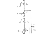
図1は、この出願の発明の第1の実施の形態を説明するためのブロック図である。同図において、11はパルス幅変調発振器、31は振動ミラーコイル励振回路、4は振動ミラーコイル(VMコイル)、51は電圧サンプラ、6はリニヤ増幅器、7はパルス立上り時点決定回路、8はピークホルダ、9はパルス立下り時点決定回路である。
【0012】
先ず、上記諸要素11〜9の構成及び動作について説明する。
パルス幅変調発振器11は、第1の変調信号入力端子a1、及び第2の変調信号入力端子a2、並びに1個の出力端子bを有する。変調信号が印加されない場合には、自励式パルス発振器として動作する。
パルス幅変調発振器11の自励発振時のパルス繰返し周波数は、第1の実施の形態では、振動ミラー(VM)の機械的共振周波数Fよりも若干低くしておく。
第1の実施の形態が前提する振動ミラー(VM)の共振周波数は50Hzであるから、パルス幅変調発振器11の自励発振時のパルス繰返し周波数は、40Hz程度にしておく。この周波数については、格別の精度は必要でない。
パルス幅変調発振器11の発振パルス列b1の波形は、図2の第3段に図示した励振パルスの電圧波形と同様である。
第1の変調信号入力端子a1に負極性の変調電圧qが印加された時は、発振パルスが立ち上がるように、第2の変調信号入力端子a2に正極性の変調電圧rが印加された時は、発振パルスが立ち下がるように、構成される。
この様なパルス幅変調発振器11は、例えば、シュミットトリガインバータと、帰還回路と、時定数回路とを組合せることによって、実現される。(詳しくは後述する。)
【0013】
振動ミラーコイル励振回路31は、振動ミラーコイル4の第1の入力端子A4に対して、励振パルス電圧を印加する。振動ミラーコイル4を流れるパルス電流は、振動ミラー(VM)に対して、印加時間に比例した角運動量を与える。
励振パルス電圧の印加開始のタイミングは、図2の第1〜第3段に図示した様に、振動ミラーの回動角θが最大点に到達した直後を選択する。励振パルス電圧の印加極性、或は振動ミラーコイル4の接続極性は、励振パルス電圧に基づくトルクが復元力として作用する方向を選択する。
振動ミラーコイル励振回路31は、増幅及びバッファ作用を有する。この回路3をスイッチング素子、例えばC−MOS・FETを用いて構成するときは、動作電圧範囲を最大限まで拡大することが出来る。
振動ミラーコイル4は、第1の入力端子A4に対して正極性の励振パルスが印加され、第2の入力端子C4に対して接地電位が供給されている時、振動ミラー(VM)に対して、同パルスの持続時間に比例した正方向の角運動量を与えるように、構成される。
【0014】
電圧サンプラ51は、励振パルスの非印加時において、振動ミラー(VM)の自由振動に起因する逆起電圧(電磁誘導電圧)を振動ミラーコイル4の第1の入力端子A4において、検出する。
かかる機能は、パルス幅変調発振器11の発振パルス列b1によって制御される禁止ゲートによって実現される。或いは、ダイオードによっても、実現される(この場合、ダイオードの極性と入力端子とは、励振パルス電圧を検出しないように選択される)。
【0015】
リニヤ増幅器6の主な役割は、電圧サンプラ51の出力(振動ミラーコイル4中に誘起された逆起電圧に比例する。)を、後段の諸回路で処理可能な振幅とするために、増幅することにある。
第2の役割は、電圧サンプラ51の出力における、有害なノイズ成分を除去することにある。即ち、ノイズフィルタとしても機能することにある。
第3の役割は、増幅率を可変とすることによって、振動ミラー(VM)の走査振幅を調整することにある。
【0016】
パルス立上り時点決定回路7は、ゼロ電圧検出回路を包含する。この回路は、電圧サンプラ51の出力電圧(即ち振動ミラー(VM)による逆起電圧の絶対値)kが、ピークからゼロになったことを検出する(図2参照)。かかる機能は、比較回路を使用することによって、実現される。
しかして、パルス立上り時点決定回路7は、ゼロ電圧を検出するや否や、パルス幅変調発振器11の第1の変調信号入力端子a1に対して、負極性の変調電圧qを印加して、同発振器11の出力電圧をゼロレベル又は低レベル(以下単に「ゼロレベル」という。)から高レベルへと反転させる。即ち、同発振器11の発振パルス列b1中の各個のパルスの立上り時点を決定する。
【0017】
ピークホルダ8は、電圧サンプラ51の各周期毎に、増幅器6の出力電圧mのピーク値を検出し且つ保持する。そして、次の励振パルスの立下り時点で、一旦ゼロレベルに復帰する。
パルス立下り時点決定回路9は、振動ミラー(VM)の所望の振幅に対応する目標値(電圧)vmとピークホルダ8から出力されたピーク電圧pmとの間の電圧差を、時間差(持続時間)に変換する機能を有する。かかる機能は、時定数回路と比較回路とを用いて実現される。(詳細は後述する。)
故に、パルス立下り時点決定回路9は、パルス幅変調発振器11の発振パルスの立上り時点を始点とし、これに時間差(持続時間)を加えて、立下り時点を決定する。そして、同発振器11の第2の変調信号入力端子a2に対して、同発振パルスを立ち下がらせるための、正極性の変調電圧rを印加する。(詳細は後述する。)
【0018】
次に、第1の実施の形態の全体的動作について説明する。
パルス幅変調発振器11は、電源が投入されると、本来のパルス繰返し周波数で発振を開始し、最初の発振パルスを出力する。
振動ミラーコイル励振回路31は、パルス幅変調発振器11から受け取った最初の発振パルスに基づいて、最初の励振パルス電圧を、振動ミラーコイル4の第1の入力端子A4に印加する。
電源投入前例えば原点(θ=0)にあった振動ミラー(VM)は、振動ミラーコイル4に流れる最初の励振パルス電流によって、正方向の角運動量が与えられる(回動角θの正・逆方向の決め方については図2参照)。振動ミラー(VM)の角速度θ′が連続的に増大し、励振パルスの終了時点で極大となる。
振動ミラー(VM)は、最初の励振パルスの終了時点で、振動モードが強制振動から自由振動に移行し、復元ばねのバネ力によって減速されながら、正方向の回動を続ける。
【0019】
最初の励振パルス電流によって振動ミラー(VM)に与えられた運動エネルギが全部復元ばね中の機械的歪みエネルギ又は磁気的ポテンシャルエネルギに変換され尽くした時点で、振動ミラー(VM)の角速度θ′は瞬間的にゼロ(静止状態)となり、その回動角θは極大値となる。
振動ミラー(VM)は、その回動角θが極大値に達した時点で復元ばねの復元力によってその回動方向が反転せしめられ、加速されながら逆方向の回動を続ける。そして、原点(θ=0)を通過して、逆方向の極大値に達する。この間、振動ミラー(VM)の角速度θ′は、原点(θ=0)を通過する時点で極大となり、その後は連続的に減速され、遂にはゼロとなる。
従って、振動ミラー(VM)の自由振動によって振動ミラーコイル4中に誘起される逆起電圧は、励振パルスが終了した時点で正の極大、回動角θが正方向の極大値に達した時点でゼロ、回動角θが原点(θ=0)を通過する時点で負極性の極大、回動角θが逆方向の極大点に達した時点で再びゼロとなる。
【0020】
説明の便のため、電圧サンプラ51は、振動ミラー(VM)の自由振動によって振動ミラーコイル4中に誘起された逆起電圧の第3番目の負極性の半波(絶対値)をその第1の入力端子A4からサンプル(抽出)することが出来たものと仮定する。リニヤ増幅器6は、サンプルされた電圧を(線形)増幅する。
パルス立上り時点決定回路7は、リニヤ増幅器6の出力(絶対値)がピークからゼロに達したこと(即ち振動ミラー(VM)の回動角θが極大値に到達したこと)を検出し、直ちにパルス幅変調発振器11の第1の変調信号入力端子a1に対して、最初の負極性の変調電圧qを印加する。
第3番目の発振パルスを出力した後、休止(ゼロ出力)状態にあったパルス幅変調発振器11は、最初の負極性の変調電圧qを受け取るや否や、その出力状態を反転させ、高電圧を出力する。即ち、第4番目の発振パルスが立ち上がる。
第4番目の発振パルスは、そのまま振動ミラーコイル励振回路31に、又、反転されてパルス立下り時点決定回路9等に送り込まれる。
一方、リニヤ増幅器6からその出力電圧(絶対値)mを受け取ったピークホルダ8は、同電圧mについて検出したピーク電圧pmをそのまま保持している。
そこで、パルス立下り時点決定回路9は、ピークホルダ8からピーク電圧pmを受け取り、パルス幅変調発振器11から第4番目の発振パルスに対応する動作許容信号(j)を受け取って、同発振器11の第4番目の(持続中の)発振パルスの持続時間、従って又、発振パルス立下り時点を決定し、同発振器11の第2の変調信号入力端子a2に対して、正極性の変調電圧rを印加する。
同時に、ピークホルダ8のピーク電圧保持状態を瞬時的に解除する。
【0021】
この間、第4回目の高出力状態にあったパルス幅変調発振器11は、正極性の変調電圧rを受け取るや否や、それ自身の出力状態を反転させて、ゼロ電圧を出力する。即ち、第4番目の出力パルスが立ち下がり、休止状態となる。
第4番目の発振パルスを受け取った振動ミラーコイル励振回路31は、振動ミラーコイル4に対して第4番目の励振パルス電圧を印加する。
第4番目の励振パルス電流によって同電流の持続時間に比例した角運動量を与えられた振動ミラー(VM)は、第4回目の振動サイクルに入る。振動ミラー(VM)の振幅(回動角極大値)は、1パルスの印加で所望の値に達することはないが、数パルスの後には、達することとなる。又、パルス幅変調発信器1 1 は、ピーク電圧の検出がなされる迄は、それ自身の周波数で発振するが、検出がなされた後は、機械的振動周波数Fに追従することとなる。
かくして、振動ミラー(VM)によって反射されたレーザビームは、所望の周期で、且つ所望の回動範囲(振幅)に亙って、正常に走査されることとなる。
【0022】
この出願の発明の第2の実施の形態による振動ミラー形走査装置用駆動回路について説明する。
同第2の実施の形態も、回動共振形振動ミラー(VM)を内包する振動ミラー形走査装置(特公平7−261109号公報参照)を前提する。回動共振形振動ミラー(VM)の諸特性は、第1の実施の形態に関連して説明した所と同様である(図5参照)。
図3は、同第2の実施の形態の概要を示すブロック図である。
同図において、12はパルス幅変調発振器、2はパルス列変換回路、32は振動ミラーコイル励振回路、4は振動ミラーコイル、52は電圧サンプラ、6は増幅器、7はパルス立上り時点決定回路、8はピークホルダ、9はパルス立下り時点決定回路である。
【0023】
先ず、上記諸要素12〜9の機能乃至動作について説明する。
図4は、第2の実施の形態の諸要素の入出力波形を示すタイミングチャートであって、同図(a)は、自励発振時(スタート時)の回路各部の入出力波形、同図(b)は、他励発振時(同期時)の回路各部の入出力波形を示すものである。
パルス幅変調発振器12は、自励発振時には、回動形振動ミラー(VM)の機械的共振周波数Fの2倍の周波数2Fよりも若干低いパルス繰返し周波数のパルス列b2を出力するように、他励発振時には、同振動ミラー(VM)の機械的共振周波数Fの2倍の周波数2Fに追従するパルス繰返し周波数の発振パルス列b2を出力することが出来るように、構成される(図4(a)の波形b、及び同図(b)の波形b参照)。
第2の実施の形態が前提する振動ミラー(VM)の共振周波数は50Hzであるから、パルス幅変調発振器12の自励発振時のパルス繰返し周波数は、80Hz程度にしておく。この周波数については、格別の精度は必要でない。
パルス幅変調発振器12のその余の事項は、パルス幅変調発振器11と同様である。(内部構成については後述する。)
【0024】
パルス列変換回路2は、発振パルス列b2を受けて、第1の変換パルス列d、第2の変換パルス列e、第3の変換パルス列f、第4の変換パルス列g、第5の変換パルス列h、第6の変換パルス列i及び第7の変換パルス列jを出力するように構成される(図4(a)の波形d〜i参照。波形jについては後述する)。
第1〜第6の変換パルス列の周期は、定常状態においては、発振パルス列b2の周期(T/2,T=1/F)の2倍(T)である。
第1の変換パルス列dの各週期は、励振期間と非励振期間とから成り、励振期間の始点は、図4(b)の如く、前の半週期の始点にあり、そのデューティ率は4分の1よりも小である。
第4の変換パルス列gの各週期は、接地期間と非接地期間とから成り、接地期間の始点は、図4(b)の如く、前の半週期の始点にあり、そのデューティ率は2分の1である。
第3の変換パルス列fの各週期は、励振期間と非励振期間とから成り、励振期間の始点は、図4(b)の如く、後の半週期の始点にあり、そのデューティ率は4分の1よりも小である。第3の変換パルス列fは、例えば、第1の変換パルス列dの位相を1/2周期(T/2=1/2F)分遅らせたものに相当する(図4のf及びd参照)。
【0025】
第2の変換パルス列eの各週期は、接地期間と非接地期間とから成り、接地期間の始点は、後の半週期の始点にあり、そのデューティ率は2分の1である。
この変換パルス列eは、例えば、第4の変換パルス列gの位相を、1/2周期(T/2=1/2F)分遅らせたものに相当する(図4のg及びe参照)。
第5の変換パルス列hの各週期は、サンプリング許容期間とサンプリング非許容期間とから成り、同サンプリング許容期間は、第1の変換パルス列dの励振期間の終了と共に開始し、前の半週期の終了と共に終了する。
第6の変換パルス列iの各週期は、サンプリング許容期間とサンプリング非許容期間とから成り、同サンプリング許容期間は、第3の変換パルス列fの励振期間の終了と共に開始し、後の半週期の終了と共に終了する。
第6の変換パルス列iは、第5の変換パルス列hの位相を1/2周期(T/2=1/2F)分遅らせたものに相当する(図4(a)のi及びh参照)。
第7の変換パルス列jの各週期は、パルス立下り時点決定回路9に対する動作許容期間と動作非許容期間とから成り、動作許容期間は、発振パルス列b2の持続期間と同一である。
【0026】
振動ミラーコイル励振回路32は、振動ミラー(VM)の回動角θが逆方向の最大点−θaに到達した直後に、振動ミラーコイル4の第1の入力端子A4に対して、第1の変換パルス列dに基づいて正極性の励振パルス電圧を印加すると共に、同ミラーコイル4の第2の入力端子C4に対して、第4の変換パルス列gに基づいて接地電位を供給するように、構成される。又、振動ミラー(VM)の回動角θが正方向の最大点θaに到達した直後に、振動ミラーコイル4の第2の入力端子C4に対して、第3の変換パルス列fに基づいて正極性の励振パルスを印加すると共に、同ミラーコイル4の第1の入力端子A4に対して、第2の変換パルス列(e)に基づいて接地電位を供給するように、構成される。
振動ミラーコイル4は、第1の入力端子A4に対して正極性の励振パルスが印加された時、同パルスの持続時間に比例した正方向の角運動量を振動ミラー(VM)に対して与えるように、又、第2の入力端子C4に対して正極性の励振パルスが印加された時、同パルスの持続時間に比例した逆方向の角運動量を同振動ミラー(VM)に対して与えるように、構成される。
【0027】
電圧サンプラ5は、第5のパルス列hの各サンプリング許容期間中に、振動ミラー(VM)の自由振動に起因する逆起電圧の正極性の半波(絶対値)を振動ミラーコイル4の第1の入力端子A4において検出し、第6のパルス列hの各サンプリング許容期間中に、逆起電圧の負極性の半波(絶対値)を、同第2の入力端子C4において検出し、それらを時間軸上で合成するように構成される。
因みに、振動ミラー(VM)の自由振動に起因する振動ミラーコイル4上の逆起電圧を第1の入力端子A4において検出する場合は、励振パルスが印加されていないこと、そして第2の入力端子C4に接地電位が供給されていることの2条件が充足されなければならない。前者の条件を充足させるためには、励振パルス電圧のデューティ率は4分の1よりも小でなければならず、後者の条件を充足させるためには、第4の変換パルスgのデューティ率は丁度2分の1でなければならない。
第2の実施の形態において使用されるリニヤ増幅器6、パルス立上り時点決定回路7、ピークホルダ8、及びパルス立下り時点決定回路9は、第1の実施の形態において使用されるものと同様である。
【0028】
次に、第2の実施の形態の全体的動作について説明する。
パルス幅変調発振器12は、電源が投入されると、本来のパルス繰返し周波数で自励発振を開始し、最初の発振パルスを出力する。
パルス列変換回路2は、最初の発振パルスを、最初の第1の変換パルスd及び第4の変換パルスg等々に変換する。
振動ミラーコイル励振回路32は、パルス列変換回路2から受け取った最初の第1の変換パルス(d)及び第4の変換パルス(g)に基づいて、最初の励振パルス電圧を、振動ミラーコイル4の第1の入力端子A4に印加する。
それまで原点(θ=0)にあった振動ミラー(VM)は、振動ミラーコイル4中に流れる最初の励振パルス電流によって正方向の角運動量が与えられる(回動角θの正・逆方向の決め方については図5参照)。振動ミラー(VM)の角速度θ′が連続的に増大し、最初の励振パルスが終了した時点で極大となる。
振動ミラー(VM)は、最初の励振パルスが終了した時点で、振動モードが強制振動から自由振動に移行し、復元ばねのバネ力によって減速されながら正方向の回動を続ける。
【0029】
最初の励振パルス電流によって振動ミラー(VM)に与えられた運動エネルギが全部復元ばね中の機械的歪みエネルギ(若しくは磁気的ポテンシャルエネルギ)に変換され尽くした時点で、振動ミラー(VM)の角速度θ′は瞬間的にゼロ(静止状態)となり、その回動角θは極大値となる。
振動ミラー(VM)は、その回動角θが極大値に達した時点で、復元ばねの復元力によってその回動方向が反転せしめられ、加速されながら逆方向の回動を続ける。そして、原点(θ=0)を通過して、逆方向の極大値に達する。この間、振動ミラー(VM)の角速度θ′は、原点(θ=0)を通過する時点で極大となり、その後は連続的に減速され、遂にはゼロとなる。
従って、振動ミラー(VM)の自由振動によって振動ミラーコイル4中に誘起される逆起電圧は、最初の励振パルスが終了した時点で正の極大、回動角θが正方向の極大値に達した時点でゼロ、回動角θが原点(θ=0)を通過する時点で負極性の極大、回動角θが逆方向の極大点に達した時点で再びゼロとなる。
【0030】
説明の便のため、電圧サンプラ52は、振動ミラー(VM)の自由振動によって振動ミラーコイル4中に誘起された逆起電圧の第2番目の正極性の半波(絶対値)を第1の入力端子A4からサンプル(抽出)することが出来たものと仮定する。リニヤ増幅器6は、電圧サンプラ52からサンプル電圧kを受け取って、(線形)増幅する。
パルス立上り時点決定回路7は、リニヤ増幅器6の出力(絶対値)がピークからゼロに達したこと(即ち振動ミラー(VM)の回動角θが正方向の極大値に達したこと)を検出し、直ちにパルス幅変調発振器12の第1の変調信号入力端子a1に対して、最初の負極性の変調電圧を印加する。
第3番目の発振パルスを出力した後休止(ゼロ出力)状態にあったパルス幅変調発振器12は、最初の負極性の変調電圧を受け取るや否や、自己の出力状態を反転させ、高電圧を出力する。即ち、第4番目の発振パルスが立ち上がる。
第4番目の発振パルスを受け取ったパルス列変換回路2は、第4番目の第1〜第4の変換パルスd〜gを振動ミラーコイル励振回路32に、同第5〜第6の変換パルスh〜iを電圧サンプラ52に、同第7の変換パルスjを、パルス立上り時点決定回路7及びパルス立下り時点決定回路9に与える。
【0031】
一方、リニヤ増幅器6から出力電圧(絶対値)mを受け取ったピークホルダ8は、同電圧mにおけるピーク値pmを検出し、そのまま保持している。
そこで、パルス立下り時点決定回路9は、ピークホルダ8からピーク電圧pmを受け取り、パルス列変換回路2から第4番目の発振パルスに対応する動作許容信号(j)を受け取って、同発振器12の第4番目の(持続中の)発振パルスの持続時間、従って又、発振パルス立下り時点を決定し、同発振器12の第2の変調信号入力端子a2に対して、正極性の変調電圧を印加する。
同時に、ピークホルダ8のピーク電圧保持状態をリセットさせる。
この間、第4番目の高出力状態にあったパルス幅変調発振器12は、パルス立下り時点決定回路8から正極性の変調電圧を受け取るや否や、その出力状態を反転させ、ゼロ電圧を出力する。即ち、第4番目の出力パルスが立ち下がる。
パルス列変換回路2から第4番目の第2の変換パルスe及び第3の変換パルスfを与えられた振動ミラーコイル励振回路32は、振動ミラーコイル4の第1の入力端子A4に対して接地電位を供給すると共に、第2の入力端子C4に対して正極性のパルス電圧を印加する。振動ミラーコイル4には、第1番目とは反対の極性の励振パルス電流が流れる。
【0032】
第4番目の励振パルス電流によって同電流の持続時間に比例した負方向の角運動量を与えられた振動ミラー(VM)は、負方向の回動を続ける。そして、原点(θ=0)を通過して、負方向の極大点に達する。振動ミラー(VM)の角速度θ′は、回動の途中、原点を通過する時点で、極大となる。
電圧サンプラ52は、振動ミラー(VM)の自由振動によって振動ミラーコイル4中に誘起された逆起電圧の第2番目の負極性の半波(絶対値)を第2の入力端子C4からサンプル(抽出)する。
逆起電圧の第2番目の負極性の半波(絶対値)のサンプル後における、リニヤ増幅器6、パルス立上り時点決定回路7、ピークホルダ8、並びにパルス立下り時点決定回路9は、第2番目の正極性の半波(絶対値)のサンプル後におけるそれらの動作と同様である。
【0033】
パルス幅変調発振器12は、パルス立上り時点決定回路7から第2番目の負極性の変調電圧を、続いてパルス立下り時点決定回路9から第2番目の正極性の変調電圧を受け取って、第3番目の発振パルスを出力する。
かくして、振動ミラー形走査装置用駆動回路全体の動作サイクルは、第1回目が終了し、第2回目に移行する。
第1回目の動作サイクルでは、励振パルスの間隔は振動ミラー(VM)の機械的振動周期Tより大、回動角θの極大値(即ち過渡状態の振幅)は定常状態の最大値より小ではあるが、それらは励振パルスが回を重ねるに連れてそれぞれ減少又は増大するから、例えば数パルス後には略定常状態に達する。
かくして、振動ミラー(VM)によって反射されたレーザビームは、所望の周期で、且つ所望の回動範囲(振幅)に亙って、正常に走査されることとなる。
【0034】
〔パルス幅変調発振器1〕、
この出願の発明の各実施の形態に使用されるパルス幅変調発振器1の内部構成の一例について説明する。
図6の(a)は、パルス幅変調発振器1の内部構成の一例を示す図である。
同図において、STはシュミットトリガインバータ、a及びbはその入力点及び出力点、R1及びR11は抵抗、D1はダイオード、C1はコンデンサである。
ダイオードD1及び抵抗R11並びに抵抗R1は、帰還回路を構成する。
コンデンサC1の充電時の時定数は、抵抗R1及びR11並びにコンデンサC1の各大きさによって決定され、放電時の時定数は、抵抗R1及びコンデンサC1の各大きさによって決定される。
この出願の発明の各実施の形態においては、放電時の時定数を、充電時の時定数よりも遥かに大きくするために、R1≫R11とする。
そして、a1は第1の変調信号入力端子、a2は第2の変調信号入力端子である。(第1の入力端子a1と入力点aとの間、及び第2の入力端子a2と入力点aとの間にはそれぞれ、ダイオードが接続されている。しかし、前段の出力インピーダンスが高いときは、それらのダイオードを省略することが出来る。そのときは、端子a1、a2及び点aの区別立ては不必要となる。)
【0035】
パルス幅変調発振器1の自励発振時の発振動作について説明する。
図6の(b)及び(C)の実線部分は、パルス幅変調発振器1の自励発振時の動作説明図である。
同図において、高入力電圧VHは第1のヒステリシス電圧、低入力電圧VLは第2のヒステリシス電圧である。第1のヒステリシス電圧VHは、例えば電源電圧VCCの約2/3程度、第2のヒステリシス電圧VLは、例えば電源電圧VCCの約1/3程度である。
シュミットトリガインバータSTの電源(図示しない)投入前(t<0)のコンデンサC1の端子電圧、即ち入力点aの電圧は、当然ゼロである。
その状態で、シュミットトリガインバータSTに電源を投入すると、出力点bの電圧が高レベルVEとなる。高レベルVEは、電源電圧VCCから若干降下した程度の値である。
出力点bの電圧が高レベルVEになると、同点bから、帰還回路のダイオードD1及び抵抗R11並びに抵抗R1を通して、コンデンサC1に電流が流入し、その端子電圧、即ち入力点aの電圧が急速に上昇する。そして、図6(b)の実線の如く、高入力レベルVH、即ち第1のヒステリシス電圧VHに達する。
【0036】
入力点aの電圧が第1のヒステリシス電圧VHを超えると、シュミットトリガインバータSTの電圧が、同図(c)の如く、反転して、ゼロレベルV0となる(この明細書では、特段の必要がない限り、ゼロレベルと低レベルを区別せず、一括して「ゼロレベル」という)。
出力点aの電圧が反転してゼロレベルになると、コンデンサC1内の電荷が抵抗素子R1を通してゆっくりと放電される。そして、図6(b)の如く、第2のヒステリシス電圧VLに達する。
入力点aの電圧が第2のヒステリシス電圧VLを下回ると、シュミットトリガインバータSTの出力電圧が、同図(c)の実線の如く、再び反転して、高レベルVHとなる。そして、コンデンサC1への充電が開始される。
以下同様にして、シュミットトリガインバータSTの反転動作が繰り返され、出力点bから発振パルス列bが出力される。
発振パルス列bのデューティ率は、抵抗R1と抵抗R11との比(R1/R11)によってほぼ決定される。
【0037】
次に、パルス幅変調発振器1の他励発振時の発振動作について説明する。
入力点aの電圧は、変調信号の入力がなければ図6(b)の実線の如く、時点1から時点4に亙って、電圧VHから電圧VLまで、ゆっくりと降下する筈である。しかし、時点2において、第1の変調信号入力端子a1に、負極性の変調電圧が印加されると、入力点aの電圧は、急激に降下して第2のヒステリシス電圧VLとなる。
すると、シュミットトリガインバータSTの出力電圧が反転して、図6(c)の点線の如く、高レベルVEになる。
出力点bの電圧が高レベルVEになると、同点bから、帰還回路の抵抗R1及びR11を通して、コンデンサC1に電荷が流入し、その端子電圧、即ち入力点aの電圧が、図6(b)の点線の如く、急速に上昇を開始する。即ち、入力点aの端子電圧は、第2のヒステリシス電圧VLから第1のヒステリシス電圧VHに向かって略直線的に上昇し、もしも変調信号の入力がなければ、同図(b)の時点3以後においても、略直線的上昇を続けるところである。しかし、同図(b)の時点3において、第2の変調信号入力端子a2に、正極性の変調電圧が印加されると、入力点aの電圧が急激に増加して、第1のヒステリシス電圧VHに到達する。
【0038】
入力点aの電圧が第1のヒステリシス電圧VHを超えると、シュミットトリガインバータSTの出力電圧が、同図(c)の点線の如く、再び反転して、ゼロレベルV0となる。
出力点bの電圧が反転してゼロレベルV0になると、コンデンサC1内の電荷が抵抗R1を通して、ゆっくりと放電され、入力点aの電圧が、図6(b)の点線の如く、ゆっくりと降下する。
そして、時点6において、第1の変調信号入力端子a1に、負極性の変調電圧が印加されると、入力点aの電圧が急激に降下し、第2のヒステリシス電圧VLとなる。すると、出力点bの電圧が再び反転して、図6(c)の点線の如く、高レベルVEとなる。
以下同様にして、シュミットトリガインバータSTの反転動作が繰り返され、出力点bから発振パルス列bが出力される。この時の発振パルス列bのパルス繰返し周波数は、第1の変調信号入力端子a1に印加される変調電圧nのパルス繰返し周波数によって規定される。
【0039】
〔パルス列変換回路2〕、
この出願の発明の第2の実施の形態に使用されるパルス列変換回路2の内部構成の一例について説明する。
図7は、パルス列変換回路2の内部構成の一例を示す図である。
同図において、2FFはDフリップフロップ、2Iはインバータ、N1、N3、N5、N6はいずれもナンド回路、VCCは電源である。
Dフリップフロップ2FFのD端子には、−Q端子の出力電圧が帰還・印加されている。
従って、Dフリップフロップ2FFは、発振パルス列bを分周して、Q端子からパルス列cを出力し、−Q端子からその反転パルス列−cを出力する。パルス列cの波形は、図4の波形cの通りであり、そのパルス繰返し周波数は、発振パルス列bのパルス繰返し周波数の2分の1である。
パルス列変換回路2は、発振パルス列bを受けて、第1の変換パルス列d、第2の変換パルス列e、第3の変換パルス列f、第4の変換パルス列g、第5の変換パルス列h、第6の変換パルス列i、及び第7の変換パルス列jを出力する。第1〜第4の変換パルス列d〜iの波形は、図4の波形d〜iの通りである。第1〜第4の変換パルス列d〜iのパルス繰返し周波数は、発振パルス列bのパルス繰返し周波数の2分の1である。
【0040】
ナンド回路N1は、パルス列cと、パルス列bとを受けて、第1のパルス列dを出力する。即ち、d=¬(c・b)。但し、記号¬は、否定を表す。
従って、パルス列dのパルス繰返し周波数は、パルス列bのパルス繰返し周波数の2分の1である。(以下同様である)。
−Q端子からの反転パルス列−cは、結節点2を経て、第2の変換パルス列eとなる。即ち、e=¬c。
ナンド回路N3は、−Q端子からの反転パルス列−cと、パルス列bとを受けて、第3の変換パルス列fを出力する。即ち、f=¬(¬c・b)。
Q端子からのパルス列cは、結節点1を経て、第4の変換パルス列gとなる。即ち、g=c。
ナンド回路N5とインバータI5との直列回路は、パルス列cと、発振パルス列bの反転パルス列−bとを受けて、第5の変換パルス列hを出力する。即ち、h=¬¬(c・−b)。
ナンド回路N6とインバータI6との直列回路は、−Q端子からの反転パルス列−cと、インバータ2Iからの発振パルス列bの反転パルス列−bとを受けて、第6の変換パルス列iを出力する。即ち、i=¬¬(−c・−b)。
【0041】
第1〜第4の変換パルス列d〜gにおいて、本質的なものは、電圧の反転時点である。同パルス列d〜gの各電圧極性は、次段の振動ミラー励振回路3の特性如何によっては、図4の極性とは反対の極性が選択されなければならない。
同様にして、変換パルス列h〜i、及びjの各電圧極性も、これを利用する電圧サンプラ5及びパルス立上り変換回路7の特性如何によっては、図4の極性とは反対の極性が選択されなければならない。
第1〜第4の変換パルス列d〜gについての正逆極性の組合せは、2の4乗、即ち16通りある。
16通りの組合せは、図7のパルス列変換回路2の出力側に、1〜4個の新たなインバータを組合せることによっても実現出来るが、新たなインバータの使用を1個だけに制限しても、実現することが出来る。
【0042】
図7のパルス列変換回路2の第1〜第4の出力パルス列をd,e,f,g、それらの組合せを(d,e,f,g)とし、d,e,f,gの各反転出力をそれぞれ、−d,−e,−f,−gとする。
第2の組合せ(−d,−e,−f,−g)は、図7に示す結節点1をQ端子から−Q端子に、同結節点2を−Q端子からQ端子に、接続替えすることによって実現される。
第3の組合せ(d,−e,−f,g)は、結節点2を−Q端子からQ端子(乃至結節点1)に接続替えすることによって、実現され、
第4の組合せ(−d,e,f,−g)は、結節点1をQ端子から−Q端子(乃至結節点2)に接続替えすることによって、実現される。
第5の組合せ(−d,e,−f,g)は、結節点3の直後にあるインバータIを、結節点3の直前に接続替えすることによって、実現される。
【0043】
第6の組合せ(d,−e,f,−g)は、第2の組合せにおける接続替えと、第5の組合せにおける接続替えとを、同時に行うことによって、実現され、
第7の組合せ(−d,−e,f,−g)は、第3の組合せにおける接続替えと、第5の組合せにおける接続替えとを、同時に行うことによって、実現され、
第8の組合せ(d,e,−f,−g)は、第4の組合せにおける接続替えと、第5の組合せにおける接続替えとを、同時に行うことによって、実現される。
第9の組合せ(−d,e,f,g)、第10の組合せ(d,−e,f,g)、第11の組合せ(d,e,−f,g)及び第12の組合せ(d,e,f,−g)は、上記第1の組合せ(d,e,f,g)における、d,e,f,gの何れか一つを、1個のインバータを用いて反転させることによって、実現される。
第13〜16の組合せは、上記第2の組合せ(−d,−e,−f,−g)における、−d,−e,−f,−gの何れか一つを、同じく1個のインバータを用いて反転させることによって、実現される。
【0044】
〔振動ミラーコイル励振回路3〕、
この出願の発明の第2の実施の形態に使用される振動ミラーコイル励振回路3の内部構成の一例について説明する。
図8は、振動ミラーコイル励振回路3の内部構成の一例を示す図である。
同図において、F1〜F4は何れもMOS・FETであって、F1及びF3はpチャネルのデプリケーション形、F2及びF4はnチャネルのデプリケーション形である。
pチャネルのデプリケーション形MOS・FET・F1及びF3のソース及びベースは、電源VCCに接続され、nチャネルのデプリケーション形MOS・FET・F2及びF4のソース及びベースは、接地電位GNDに接続される。
即ち、ホイートストンブリッジの上部頂点には電源VCCが接続され、下部頂点には接地電位GNDが接続され、同ブリッジの各辺にはそれぞれMOS・FET・F1〜F4が接続される。そして、左右の頂点は、振動ミラーコイル4の第1及び第2の入力端子A4及びC4に接続される。
【0045】
pチャネルのMOS・FET・F1及びF3は、ベースに印加されたゲート電圧が正のゲート閾(しきい)値電圧VT以下の時オンとなり、同ゲート電圧が負極性の大きな値になった時はソースSからドレーンDに大きな飽和電流が流れるが、同ゲート電圧がゲート閾値電圧VT以上の正極性の電圧になった時は、ソース・ドレーン間に電流は流れない。
nチャネルのMOS・FET・F2及びF4は、ベースに印加されたゲート電圧が負のゲート閾値電圧VT以上の時オンとなり、同ゲート電圧が正極性の大きな値になった時はドレーンDからソースSに大きな飽和電流が流れるが、同ゲート電圧がゲート閾値電圧VT以上の正極性の電圧になった時は、ソース・ドレーン間に電流は流れない。
【0046】
従って、図8の振動ミラー励振回路3に印加された変換パルスd、e、f、gの電圧極性の組合せが図4の如く(O,O,H,H)の期間中、点A、Bの電圧極性の組合せは(H,O)であり、
同変換パルスd〜gの電圧極性の組合せが図4の如く(H,O,H,H)の期間中、点A、Bの電圧極性の組合せは(*,0)であり、
同変換パルスd〜gの電圧極性の組合せが図4の如く(H,H,O,O)の期間中、点A、Bの電圧極性の組合せは(O,H)であり、
同変換パルスd〜gの電圧極性の組合せが図4の如く(H,H,H,O)の期間中、点A、Bの電圧極性の組合せは(0,*)である。
ここに記号*は、次段の振動ミラーコイル4中の逆起電力の有無に依存することを示す。
なお、図8の振動ミラー励振回路3に使用したMOS・FET・F1は、ゲート入力電圧dが負極性の時に導通する形式のスイッチング素子であるが、この素子F1を、第1の変換パルス列dの代りにその反転パルス列−dが入力されることを条件として、入力電圧が正極性の時に導通する形式のスイッチング素子(例えばnチャネルのエンハンスメント形MOS・FET)で、置換することが出来る。同様に、MOS・FET・F2、F3及びF4もそれぞれ、入力電圧の極性がそれらとは反転関係にある時に導通する形式のスイッチング素子で、置換することが出来る。
置換の組合せは、2の4乗、即ち16通りある。
【0047】
〔電圧サンプラ5 2 〕、
この出願の発明の第2の実施の形態に使用される電圧サンプラ5 2 の内部構成の一例について説明する。
図9は、電圧サンプラ5 2 の内部構成の一例を示す図である。
同図において、5S1は第1のアナログスイッチ(伝送ゲート)、5S2は第2のアナログスイッチ(伝送ゲート)である。これらのアナログスイッチは、制御端子Cに正極性の制御電圧が印加されている間、入出力端子AB間が導通状態となる形式のものである。
第1のアナログスイッチ5S1は、制御端子Cに印加された第5の変換パルス列hのオン期間(即ち励振パルスの非印加期間)に、振動ミラーコイル4の第1の入力端子A4に現れた逆起電圧(アナログ電圧)を検出することが出来る。又、第2のアナログスイッチ5S2は、制御端子Cに印加された第6の変換パルス列iのオン期間(即ち励振パルスの非印加期間)に、振動ミラーコイル4の第2の入力端子C4に現れた逆起電圧(アナログ電圧)を、検出することが出来る。
アナログスイッチ5S1及び5S2によって検出された各起電圧は、同スイッチ5S1及び5S2の出力側で合成される。
スイッチ5S1が、負極性の制御電圧印加時に導通する形式のものである場合は、同スイッチ5S1の制御端子Cに印加される変換パルス列は、第5の変換パルス列hの反転パルス列−hでなければならない。このことは、スイッチ5S2についても同様である。
【0048】
〔パルス立上り時点決定回路7〕、
この出願の発明の各実施の形態に使用されるパルス立上り時点決定回路7の内部構成の一例について説明する。
図10は、パルス立上り時点決定回路7の内部構成の一例を示す図である。
同図において、7COは比較器、R71、R72、R73及びR74は何れも抵抗素子である。これらの諸素子は、共同してゼロ検出器を構成する。
そして、7FFはDフリップフロップである。
スタート時点では、結節点1には、基準電圧Vrによって、微小電圧(R72/R71)Vrが与えられ、比較器7COの+端子には、略この電圧が、与えられている。各抵抗素子の値が、R72≫R71、R72≒R73、R72≫R73、R74≫R71、R74≫R73となるように、選択されているからである。従って、比較器7COの出力電圧は、高レベル(電源電圧VCCの程度)となる(図4の(b)参照)。
又、Dフリップフロップ7FFの−Q端子の出力電圧は、スタート時点では、高レベルとなるように、設定されている。
【0049】
振動ミラーの自由振動による逆起電圧が検出され、増幅器6の出力電圧mが、比較器7COの−端子に与えられると、その出力電圧nは、反転してゼロレベルとなる。続いて、増幅器6の出力電圧mが、増大し、極大値に達し、反転後減少を開始するが、比較器7COの出力電圧nは、変化しない。
増幅器6の出力電圧mが、ゼロレベルに降下すると、比較器7COの出力電圧nは、反転して、高レベルとなる。
すると、Dフリップフロップ7FFの状態が反転して、−Q端子の出力電圧が負極性となる。そして、次段のパルス幅変調発振器1の第1の変調入力端子a1に対して、負電圧を印加する。
パルス幅変調発振器1の出力電圧が、ゼロレベルから高レベルに反転した後、高レベルからゼロレベルに反転し、従って、信号列変換回路2の第7の変換パルス列jが高レベルとなると、Dフリップフロップ7FFの状態が反転して、出力端子−Qの出力電圧が高レベルとなる。
以下、同様にして、−Q端子の出力電圧が高レベルからゼロレベルへ、そしてゼロレベルから高レベルからへ、という反転動作を繰り返す。
【0050】
〔ピークホルダ8〕、
この出願の発明の各実施の形態に使用されるピークホルダ8の内部構成の一例について説明する。
図11は、ピークホルダ8及びパルス立下り時点決定回路9並びに帰還回路10の内部構成の一例を示す図である。
図11の右半部において、8DAは差動増幅器、D81はダイオード、R81は抵抗素子、C8はコンデンサ、L8は帰還ループ、8Sはアナログスイッチ、R82は接地抵抗、D82は定電圧ダイオードである。
アナログスイッチ8Sは、制御入力端子Cにゼロ電位乃至正電位が供給されている間、入出力端子AB間が不導通状態、同制御入力端子Cに負極性の制御電圧が印加されている間、同出力端子AB間が導通状態となる。
抵抗素子R82は、アナログスイッチ8Sの制御入力端子Cに常時ゼロ電位を供給するためのもの、ダイオードD82は、パルス電圧の大きさを一定にするためのものである。
上記の差動増幅器8DA、ダイオードD81、抵抗素子R81、コンデンサC8、帰還ループL8及びアナログスイッチ8S、抵抗素子R82、及びダイオードD82は、共同して、ピークホルダ8を構成する。
【0051】
増幅器6の出力電圧mが差動増幅器8DAの+端子に印加されると、ダイオードD81と抵抗R81を介して充電電流が流れ、コンデンサC8が充電される。そして、+端子への印加電圧と−端子への帰還電圧との間の電圧差が正である間は、その電圧差に比例した充電電流が、ダイオードD81と抵抗R81を介して、コンデンサC8に流入し、その端子電圧pを上昇させ続ける。
かくして、コンデンサC8の端子電圧p、即ち、ピークホルダ8の出力電圧pは、図4(b)の波形pの如く、増幅器6の出力電圧mにおけるピーク値pmを保持することとなる。
ピークホルダ8の保持電圧は、アナログスイッチ8Sの制御入力端子Cに負極性のパルス電圧が印加された時、ピーク値pmからゼロレベルに復帰せしめられる。
なお、図11のアナログスイッチ8Sの代りに、制御入力端子Cに正極性の制御電圧が印加された時に導通状態となるような制御特性のアナログスイッチを、使用することが出来る。
【0052】
〔パルス立下り時点決定回路9〕、
この出願の発明の各実施の形態に使用されるパルス立下り時点決定回路9の内部構成の一例について説明する。
図11の左半部において、9Sはアナログスイッチ、9COは比較器、91はインバータ、C9はコンデンサ、R91、R92及びR93は抵抗素子である。
パルス幅変調発振器1の出力電圧が低レベル、従って、パルス列変換回路2からの第7の変換パルス列jが高レベルの時は、アナログスイッチ9Sが導通状態にあるから、コンデンサC9は、基準電圧Vrによって充電され、その端子電圧qは、定常状態においては、Vr・R91/(R91+R92)(以下「目標値vm」という。)となる。
【0053】
パルス幅変調発振器1の出力電圧が低レベルから高レベルに、従ってパルス列変換回路2の第7の変換パルス列が高レベルから低レベルに反転すると、アナログスイッチ9Sが不導通状態となるから、コンデンサC9が放電を開始し、その端子電圧qが急速に降下する。コンデンサC9の端子電圧qが降下して、ピークホルダ8からのピーク電圧pmを下回ると、比較器9COの出力が反転して、ゼロレベルとなり、インバータ9Iの出力が高レベルとなる。
コンデンサC9が放電を開始してから比較器9COの出力が反転するまでの時間間隔は、目標値vmとピーク値pmとの間の電圧差(vm−pm)に略比例する。従って、振動ミラー(VM)の所望の振幅と、実際の振幅(測定時の振幅)との振幅差に比例することとなる。
【0054】
かくして、パルス立下り時点決定回路9は、比較器9COの出力が反転した時点で、次段のパルス幅変調発振器1の第2の変調信号入力端子a2に正極性の変調電圧rを印加して、同発振器1の発振パルスを立ち下げる。
同時に、帰還回路10を介して、前段のピークホルダ8のアナログスイッチ8Sの制御入力端子Cに、負極性のパルス電圧を印加する。すると、同スイッチ8Sの入出力端子AB間が導通状態となるから、これを介してコンデンサC8の電化が放電され、その端子電圧qは、短時間ゼロレベルになる。
上記の帰還回路10は、直列接続されたインバータ10I及び結合コンデンサC10から成る。
なお、前段のピークホルダ8におけるアナログスイッチ8Sとして、制御入力端子Cに正極性の制御電圧が印加された時に導通状態となるような制御特性のアナログスイッチが使用されている場合には、帰還回路10のインバータ10Iを省略することが出来る。その場合は、定電圧ダイオードD82の極性を反転させなければならない。
【0055】
【発明の効果】
この出願の発明は、以上のように構成したから、下記の通り、顕著な効果を奏することができる。
(a)振動ミラー(VM)を共振モードで動作せしめることが出来、しかも振動ミラー(VM)の回動角(位置)及び角速度を直接検出する為のセンサを必要としない、振動ミラー形走査装置用駆動回路を提供することが出来る。 (b)振動ミラー(VM)を共振モードで動作せしめると共に、同振動ミラー(VM)の回動角(位置)及び角速度を直接検出するセンサを使用すること無しに、駆動電圧の周波数及び位相を、振動ミラー(VM)の機械的共振周波数及び位相に自動的に追従させることが出来る、調整不要の、振動ミラー形走査装置用駆動回路を提供することが出来る。
(c)パルス電圧(電流)で振動ミラーコイルを駆動すると共に、当該パルス電圧(電流)を振動ミラー(VM)の機械的振動に自動的に同期させることより、消費電流及び消費電力を最小化し、以って使用電池の長寿命化を実現することが出来る、振動ミラー形走査装置用駆動回路を提供することが出来る。
(d)パルス電圧(電流)で振動ミラーコイルを励振することによって、動作電圧の範囲を極限まで拡大することが出来る、振動ミラー形走査装置用駆動回路を提供することが出来る。
【図面の簡単な説明】
【図1】この出願の発明の第1の実施の形態による振動ミラー形走査装置用駆動回路の全体構成を示すブロック図である。
【図2】第1の実施の形態における振動ミラーの動作説明図である。
【図3】この出願の発明の第2の実施の形態による振動ミラー形走査装置用駆動回路の全体構成を示すブロック図である。
【図4】第2の実施の形態の諸要素の入出力波形を示す図である。
【図5】第2の実施の形態における振動ミラーの動作説明図である。
【図6】各実施の形態に使用されるパルス幅変調発振器の内部構成を示す図である。
【図7】第2の実施の形態に使用されるパルス列変換回路の内部構成を示す図である。
【図8】同振動ミラーコイル励振回路の内部構成を示す図である。
【図9】同電圧サンプラの内部構成を示す図である。
【図10】各実施の形態に使用されるパルス立上り時点決定回路の内部構成を示す図である。
【図11】同ピークホルダ及びパルス立下り時点決定回路並びに帰還回路の各内部構成を示す図である。
【符号の説明】
11パルス幅変調発振器
12パルス幅変調発振器
2 パルス信号列変換回路
3 振動ミラーコイル励振回路
4 振動ミラーコイル(VMコイル)
5 電圧サンプラ
6 増幅器
7 パルス立上り時点決定回路
8 ピークホルダ
9 パルス立下り時点決定回路
10 帰還回路
ST シュミットトリガインバータ
2FF Dフリップフロップ
F1 MOS・FET(例えばpチャネルのデプリケーション形)
F2 MOS・FET(例えばnチャネルのデプリケーション形)
F3 MOS・FET(例えばpチャネルのデプリケーション形)
F4 MOS・FET(例えばnチャネルのデプリケーション形)
5S1 第1のアナログスイッチ
5S2 第2のアナログスイッチ
7CO 比較器
7FF Dフリップフロップ
8DA 差動増幅器
8S アナログスイッチ
9S アナログスイッチ
9CO 比較回路[0001]
BACKGROUND OF THE INVENTION
The invention of this application relates to a drive circuit for a vibrating mirror type scanning device for driving a vibrating mirror type scanning device used in an optical information reader.
[0002]
[Prior art]
Rotating mirrors used in optical information readers are roughly classified into non-vibrating mirrors and vibrating mirrors. Here, the non-vibrating mirror is a type of mirror that repeats rotation-stop-rotation-stop during the optical information reading operation, and the vibration mirror does not stop during the reading operation. A mirror that continues to vibrate.
The oscillating mirror used in the optical information reader has a unique mechanical resonance frequency. Such a driving method of the oscillating mirror is roughly classified into an asynchronous type and a synchronous type. Here, the asynchronous driving method is a method in which the frequency of the voltage (current) to be applied (supplied) to the oscillating mirror scanning apparatus is greatly detuned (separated) from the mechanical resonance frequency of the oscillating mirror. The synchronous driving method is a method of matching the frequency and phase of the voltage to be applied to the vibrating mirror scanning device with the mechanical frequency and phase of the vibrating mirror, respectively.
In the latter driving method, an analog type using a sine wave voltage or a sawtooth voltage as an applied voltage has been proposed.
In addition, a sensor for directly detecting the rotational position and angular velocity of the vibrating mirror is introduced, and the frequency of the drive voltage to be applied to the scanning device of the vibrating mirror using the detection output of the sensor is introduced. Has been proposed to automatically follow the mechanical resonance frequency of the vibrating mirror.
[0003]
[Problems of conventional technology]
However, according to the research of the inventors of this application, it has been clarified that the conventional driving method has the following drawbacks and problems.
First, the introduction of a sensor for directly detecting the rotational position and angular velocity of the vibrating mirror increases the product cost.
Second, if the detection output of the sensor is used to automatically make the drive voltage frequency follow the natural resonance frequency of the oscillating mirror, after the sensor is incorporated, the adjustment of the entire circuit is performed again. Necessary.
Thirdly, in the analog driving method (driving method using, for example, a sine wave voltage or a sawtooth wave voltage as a driving voltage), current or power is not consumed so that it is difficult to extend the life of the battery used. It is.
Fourth, when a sine wave voltage or a sawtooth wave voltage is used as the drive voltage, it is difficult to widen the range of the operating voltage to the limit.
[0004]
OBJECT OF THE INVENTION
Therefore, the first object of the invention of this application is to provide a sensor that can operate the vibration mirror (VM) in the resonance mode and directly detect the rotational position and angular velocity of the vibration mirror (VM). An object of the present invention is to provide a drive circuit for a vibrating mirror type scanning device which is not required.
The second object of the invention of this application is to operate the oscillating mirror (VM) in the resonance mode, and without using a sensor that directly detects the rotational position and angular velocity of the oscillating mirror (VM). It is an object of the present invention to provide a drive circuit for a oscillating mirror type scanning device that can automatically follow the frequency and phase of the oscillating mirror (VM) with the mechanical resonance frequency and phase of the oscillating mirror (VM) and does not require adjustment.
The third object of the invention of this application is to excite the oscillating mirror coil with a pulse voltage and to automatically synchronize the pulse voltage with the mechanical oscillation of the oscillating mirror (VM). It is an object of the present invention to provide a drive circuit for a vibrating mirror type scanning device that can realize a long life of a battery used.
A fourth object of the invention of this application is to provide a drive circuit for a oscillating mirror type scanning device capable of expanding the range of the operating voltage to the limit by exciting the oscillating mirror coil with a pulse voltage. .
[0005]
[Means for achieving the objectives]
In order to solve the above problems and achieve the above object,
The drive circuit for the vibrating mirror type scanning device according to the first embodiment of the invention of this application is:
Pulse width modulation oscillator 11A vibrating mirror
Pulse
Vibration mirror
The vibrating
The pulse rise time determination circuit 7 includes a
The peak holder 8 is the
The pulse falling
[0006]
According to the vibration mirror type scanning device driving circuit of the first embodiment of the present invention, the pulse
The oscillating mirror (VM) is given a positive angular momentum by the
The back electromotive force due to free vibration of the oscillating mirror (VM) is the maximum point θ in which the rotation angle θ of the mirror (VM) is positive.a, And the maximum point in the reverse direction -θaWhen it reaches, it instantaneously becomes zero. The pulse rising point determination circuit 7 determines that the rotation angle θ of the oscillating mirror (VM) is the maximum point −θ in the reverse direction.aAt the point of time (hence the
Thus, the pulse
[0007]
Vibration mirror (VM) amplitude (rotation range) θaIs the maximum value θ ′ of the angular velocity θ ′ during free vibration.max(Appears at θ = 0). The angular velocity θ ′ of the vibrating mirror (VM) is the maximum value θ ′maxWhen reaching, the back electromotive force also reaches its peak. The peak value of the back electromotive force is the
That is, the actual amplitude θ of the vibrating mirror (VM)aThe smaller is the desired amplitude, the longer the duration of the excitation pulse and the greater the angular momentum, and hence the greater the kinetic energy, to the vibrating mirror (VM).
Thus, the duration of the oscillation pulse, and thus the duration of the excitation pulse, is automatically adjusted by the pulse fall
[0008]
The drive circuit for the vibrating mirror type scanning device according to the second embodiment of the invention of this application is:
Pulse width modulation oscillator 12A pulse
The pulse
The pulse
The period of the first to sixth conversion pulse trains is the oscillation pulse train b in a steady state.2Twice the period (T / 2, T = 1 / F) (T),
Each week period of the first converted pulse train d is composed of an excitation period and a non-excitation period. The start point of the excitation period is at the start point of the previous half-week period, and the duty ratio is less than a quarter. ,
Each week period of the fourth conversion pulse train g is composed of a ground period and a non-ground period, the start point of the ground period is at the start point of the previous half-week period, and the duty ratio is ½,
Each week period of the third conversion pulse train f is composed of an excitation period and a non-excitation period. The start point of the excitation period is at the start point of the subsequent half-week period, and the duty ratio is smaller than a quarter. ,
Each week period of the second conversion pulse train e is composed of a ground period and a non-ground period, the start point of the ground period is at the start point of the subsequent half-week period, and the duty ratio is ½,
Each week period of the fifth converted pulse train h is composed of a sampling allowable period and a sampling non-permissible period, and the sampling allowable period starts with the end of the excitation period of the first converted pulse train d, and the previous half-week period Ends with the end of
Each week period of the sixth converted pulse train i is composed of a sampling allowable period and a sampling non-permissible period, and the sampling allowable period starts with the end of the excitation period of the third converted pulse train f, and the subsequent half-week period Ends with the end of
Each week period of the seventh converted pulse train j is composed of an operation allowable period and an operation non-permissible period for the pulse falling
The vibrating mirror
The vibrating
The pulse rise time determination circuit 7 includes the
The peak holder 8 includes the
The pulse falling
[0009]
According to the drive circuit for the vibrating mirror type scanning device of the second embodiment of the present invention, the pulse
The oscillating mirror (VM) has a maximum angle −θ whose rotation angle θ is in the opposite direction.aImmediately after reaching the first input terminal A of the vibrating
The back electromotive force due to free vibration of the oscillating mirror (VM) is the maximum point θ in which the rotation angle θ of the mirror (VM) is positive.aThe maximum point -θ in the opposite directionaWhen it reaches, it instantaneously becomes zero.
The pulse rise time determination circuit 7 includes a
Thus, the pulse
[0010]
Vibration mirror (VM) amplitude (rotation range) θaIs the maximum value θ ′ of the angular velocity θ ′ during free vibration.max(Appears at θ = 0). The angular velocity θ ′ of the vibrating mirror (VM) is the maximum value θ ′maxWhen reaching, the back electromotive force also reaches its peak. The peak value of the back electromotive force is the
The pulse falling
That is, the actual amplitude θ of the vibrating mirror (VM)aThe smaller is the desired amplitude, the longer the duration of the excitation pulse and the greater the angular momentum, and hence the greater the kinetic energy, to the vibrating mirror (VM).
Thus, the duration of the oscillation pulse, and thus the duration of the excitation pulse, is automatically adjusted by the pulse fall
[0011]
DETAILED DESCRIPTION OF THE INVENTION
The configuration of the drive circuit for the vibrating mirror type scanning device according to the first embodiment of the invention of this application will be described.
The first embodiment is premised on a vibrating mirror type scanning device (see, for example, Japanese Patent Laid-Open No. 7-261109) including a rotating resonance type vibrating mirror (VM).
For example, the rotating resonance type oscillating mirror (VM) receives a rotational force by a drive current flowing through the oscillating mirror coil. On the other hand, it receives a restoring force by a mechanical spring force or a magnetic spring force.
The rotational resonance type oscillating mirror (VM), once given angular momentum, generates free vibration at the mechanical resonance frequency F, and the rotational angle θ is a period T (= 1 / F). As shown in the first stage of FIG. At that time, a counter electromotive voltage that changes like a sine wave appears between the terminals of the oscillating mirror coil due to electromagnetic induction as illustrated in the lowermost stage of FIG.
FIG. 1 is a block diagram for explaining a first embodiment of the invention of this application. In the figure, 11Is a pulse width modulation oscillator, 31Is a vibrating mirror coil excitation circuit, 4 is a vibrating mirror coil (VM coil), 51Is a voltage sampler, 6 is a linear amplifier, 7 is a pulse rise time determination circuit, 8 is a peak holder, and 9 is a pulse fall time determination circuit.
[0012]
First, the
Pulse
Pulse
Since the resonance frequency of the oscillating mirror (VM) assumed in the first embodiment is 50 Hz, the pulse
Pulse
First modulation signal input terminal a1When a negative modulation voltage q is applied to the second modulation signal input terminal a, the oscillation pulse rises.2When a positive modulation voltage r is applied to the oscillation pulse, the oscillation pulse falls.
Such a pulse
[0013]
Vibration mirror
The timing of starting application of the excitation pulse voltage is selected immediately after the rotation angle θ of the vibrating mirror reaches the maximum point, as shown in the first to third stages of FIG. The applied polarity of the excitation pulse voltage or the connection polarity of the
Vibration mirror
The vibrating
[0014]
Such a function is achieved by the pulse
[0015]
The main role of the
The second role is the
The third role is to adjust the scanning amplitude of the oscillating mirror (VM) by making the amplification factor variable.
[0016]
The pulse rising point determination circuit 7 includes a zero voltage detection circuit. This circuit is a
Therefore, as soon as the pulse rise time determination circuit 7 detects the zero voltage, the pulse
[0017]
The peak holder 8 is a
The pulse falling
Therefore, the pulse falling
[0018]
Next, the overall operation of the first embodiment will be described.
Pulse
Vibration mirror
For example, the vibrating mirror (VM) at the origin (θ = 0) before power-on is given a positive angular momentum by the first excitation pulse current flowing through the vibrating mirror coil 4 (forward / reverse rotation angle θ). (See Figure 2 for how to determine the direction). The angular velocity θ ′ of the oscillating mirror (VM) continuously increases and reaches a maximum at the end of the excitation pulse.
The vibration mirror (VM) continues to rotate in the forward direction while the vibration mode shifts from forced vibration to free vibration at the end of the first excitation pulse and is decelerated by the spring force of the restoring spring.
[0019]
When the kinetic energy given to the vibrating mirror (VM) by the first excitation pulse current is completely converted into mechanical strain energy or magnetic potential energy in the restoring spring, the angular velocity θ ′ of the vibrating mirror (VM) is It instantaneously becomes zero (stationary state), and the rotation angle θ becomes a maximum value.
When the rotational angle θ reaches the maximum value, the vibrating mirror (VM) is reversed in its rotating direction by the restoring force of the restoring spring, and continues to rotate in the reverse direction while being accelerated. Then, it passes through the origin (θ = 0) and reaches the maximum value in the reverse direction. During this time, the angular velocity θ ′ of the oscillating mirror (VM) becomes maximum when it passes through the origin (θ = 0), and thereafter is continuously decelerated and finally becomes zero.
Therefore, the counter electromotive voltage induced in the vibrating
[0020]
For convenience of explanation,
The pulse rising point determination circuit 7 detects that the output (absolute value) of the
After outputting the third oscillation pulse, the pulse
The fourth oscillation pulse is directly applied to the vibrating mirror
On the other hand, the peak holder 8 that has received the output voltage (absolute value) m from the
Therefore, the pulse falling
At the same time, the peak voltage holding state of the peak holder 8 is released instantaneously.
[0021]
During this period, the pulse
The vibrating mirror
The vibrating mirror (VM) given the angular momentum proportional to the duration of the current by the fourth excitation pulse current enters the fourth vibration cycle. The amplitude (rotation angle maximum value) of the oscillating mirror (VM) does not reach a desired value when one pulse is applied, but reaches a desired value after several pulses. Pulse width modulation transmissionvessel1 1 Oscillates at its own frequency until the peak voltage is detected, but after the detection, the mechanical vibration frequencyNumber FWill follow.
Thus, the laser beam reflected by the oscillating mirror (VM) is normally scanned at a desired period and over a desired rotation range (amplitude).
[0022]
A drive circuit for a vibrating mirror type scanning device according to a second embodiment of the invention of this application will be described.
The second embodiment also presupposes a vibrating mirror type scanning device (see Japanese Patent Publication No. 7-261109) including a rotating resonance type vibrating mirror (VM). Various characteristics of the rotating resonance type oscillating mirror (VM) are the same as those described in connection with the first embodiment (see FIG. 5).
FIG. 3 is a block diagram showing an outline of the second embodiment.
In the figure, 12Is a pulse width modulation oscillator, 2 is a pulse train conversion circuit, 32Is a vibrating mirror coil excitation circuit, 4 is a vibrating mirror coil, 52Is a voltage sampler, 6 is an amplifier, 7 is a pulse rise time determination circuit, 8 is a peak holder, and 9 is a pulse fall time determination circuit.
[0023]
First, the
FIG. 4 is a timing chart showing input / output waveforms of various elements of the second embodiment. FIG. 4 (a) shows input / output waveforms of each part of the circuit during self-excited oscillation (starting). (B) shows input / output waveforms of each part of the circuit during separately excited oscillation (during synchronization).
Pulse
Since the resonance frequency of the oscillating mirror (VM) assumed in the second embodiment is 50 Hz, the pulse
Pulse
[0024]
The pulse
The period of the first to sixth conversion pulse trains is the oscillation pulse train b in the steady state.2The period (T / 2, T = 1 / F) is twice (T).
Each week period of the first converted pulse train d is composed of an excitation period and a non-excitation period. The start point of the excitation period is at the start point of the previous half-week period as shown in FIG. 4B, and the duty ratio is 4 minutes. Less than 1.
Each week period of the fourth conversion pulse train g is composed of a ground period and a non-ground period. The start point of the ground period is at the start point of the previous half-week period as shown in FIG. 4B, and the duty ratio is 2 minutes. 1 of
Each week period of the third conversion pulse train f is composed of an excitation period and a non-excitation period, and the start point of the excitation period is at the start point of the subsequent half week period as shown in FIG. Less than 1. The third conversion pulse train f corresponds to, for example, a phase obtained by delaying the phase of the first conversion pulse train d by ½ period (T / 2 = ½F) (see f and d in FIG. 4).
[0025]
Each week period of the second conversion pulse train e is composed of a ground period and a non-ground period. The start point of the ground period is at the start point of the subsequent half-week period, and the duty ratio is ½.
This conversion pulse train e corresponds to, for example, a phase obtained by delaying the phase of the fourth conversion pulse train g by ½ period (T / 2 = ½F) (see g and e in FIG. 4).
Each week period of the fifth converted pulse train h is composed of a sampling allowable period and a sampling non-permissible period. The sampling allowable period starts with the end of the excitation period of the first converted pulse train d and ends the previous half-week period. Finish with.
Each week period of the sixth converted pulse train i is composed of a sampling allowable period and a sampling non-permissible period. The sampling allowable period starts with the end of the excitation period of the third converted pulse train f and ends with the subsequent half-week period. Finish with.
The sixth conversion pulse train i corresponds to a phase obtained by delaying the phase of the fifth conversion pulse train h by ½ period (T / 2 = 1 / 2F) (see i and h in FIG. 4A).
Each week period of the seventh converted pulse train j is composed of an operation allowable period and an operation non-permissible period for the pulse falling
[0026]
Vibration mirror
The vibrating
[0027]
The
Incidentally, the back electromotive voltage on the vibrating
The
[0028]
Next, the overall operation of the second embodiment will be described.
Pulse
The pulse
Vibration mirror
The oscillating mirror (VM) which has been at the origin (θ = 0) until then is given a positive angular momentum by the first excitation pulse current flowing in the oscillating mirror coil 4 (in the forward and reverse directions of the rotation angle θ) (See Figure 5 for how to decide). The angular velocity θ ′ of the oscillating mirror (VM) continuously increases and reaches a maximum when the first excitation pulse is completed.
When the first excitation pulse ends, the vibration mirror (VM) shifts from the vibration mode to the free vibration and continues to rotate in the positive direction while being decelerated by the spring force of the restoring spring.
[0029]
When the kinetic energy given to the vibrating mirror (VM) by the first excitation pulse current is completely converted into mechanical strain energy (or magnetic potential energy) in the restoring spring, the angular velocity θ of the vibrating mirror (VM) ′ Instantaneously becomes zero (stationary state), and the rotation angle θ has a maximum value.
When the rotation angle θ reaches the maximum value, the vibrating mirror (VM) is reversed in its rotating direction by the restoring force of the restoring spring, and continues to rotate in the reverse direction while being accelerated. Then, it passes through the origin (θ = 0) and reaches the maximum value in the reverse direction. During this time, the angular velocity θ ′ of the oscillating mirror (VM) becomes maximum when it passes through the origin (θ = 0), and thereafter is continuously decelerated and finally becomes zero.
Therefore, the counter electromotive voltage induced in the
[0030]
For convenience of explanation,
The pulse rise time determination circuit 7 detects that the output (absolute value) of the
After outputting the third oscillation pulse, the pulse
Upon receiving the fourth oscillation pulse, the pulse
[0031]
On the other hand, the peak holder 8 that has received the output voltage (absolute value) m from the
Therefore, the pulse falling
At the same time, the peak voltage holding state of the peak holder 8 is reset.
During this period, the pulse
The vibrating mirror
[0032]
The oscillating mirror (VM) given the negative angular momentum proportional to the duration of the current by the fourth excitation pulse current continues to rotate in the negative direction. Then, it passes through the origin (θ = 0) and reaches the maximum point in the negative direction. The angular velocity θ ′ of the oscillating mirror (VM) becomes a maximum when passing through the origin during the rotation.
After the second negative half wave (absolute value) of the back electromotive voltage is sampled, the
[0033]
Pulse
Thus, the entire operation cycle of the drive circuit for the oscillating mirror type scanning device ends at the first time and shifts to the second time.
In the first operation cycle, the excitation pulse interval is larger than the mechanical vibration period T of the oscillating mirror (VM), and the maximum value of the rotation angle θ (that is, the amplitude in the transient state) is smaller than the maximum value in the steady state. There are each, as the excitation pulse repeatsDecreaseOr, since it increases, for example, a substantially steady state is reached after several pulses.
Thus, the laser beam reflected by the oscillating mirror (VM) is normally scanned at a desired period and over a desired rotation range (amplitude).
[0034]
[Pulse width modulation oscillator 1],
An example of the internal configuration of the pulse
FIG. 6A is a diagram illustrating an example of the internal configuration of the pulse
In the figure, ST is a Schmitt trigger inverter, a and b are its input and output points, and R1And R11Is resistance, D1Is a diode, C1Is a capacitor.
Diode D1And resistance R11And resistance R1Constitutes a feedback circuit.
Capacitor C1The time constant when charging is the resistance R1And R11And capacitor C1The time constant during discharge is determined by the resistance R1And capacitor C1Is determined by each size.
In each embodiment of the invention of this application, in order to make the time constant at the time of discharging much larger than the time constant at the time of charging, R1≫R11And
And a1Is a first modulation signal input terminal, a2Is a second modulation signal input terminal. (First input terminal a1And the input point a, and the second input terminal a2Are connected to the input point a. However, when the output impedance of the previous stage is high, these diodes can be omitted. At that time, terminal a1, A2And the distinction of point a becomes unnecessary. )
[0035]
The oscillation operation during self-excited oscillation of the pulse
6B and 6C are diagrams for explaining the operation of the pulse
In the figure, the high input voltage VHIs the first hysteresis voltage, low input voltage VLIs the second hysteresis voltage. First hysteresis voltage VHFor example, the power supply voltage VCCAbout 2/3 of the second hysteresis voltage VLFor example, the power supply voltage VCCIt is about 1/3 of.
Capacitor C before power supply (not shown) of Schmitt trigger inverter ST (t <0)1The terminal voltage of I, ie, the voltage at the input point a is naturally zero.
In this state, when the power is supplied to the Schmitt trigger inverter ST, the voltage at the output point b becomes high level V.EIt becomes. High level VEIs the power supply voltage VCCIt is a value that is slightly lowered from.
The voltage at the output point b is high level VEThen, from the same point b, the diode D of the feedback circuit1And resistance R11And resistance R1Through capacitor C1Current flows into the terminal, and its terminal voltage, that is, the voltage at the input point a rises rapidly. As shown by the solid line in FIG. 6B, the high input level VHThat is, the first hysteresis voltage VHTo reach.
[0036]
The voltage at the input point a is the first hysteresis voltage VHWhen the voltage exceeds the Schmitt trigger inverter ST, the voltage is inverted as shown in FIG.0(In this specification, unless specifically required, the zero level and the low level are not distinguished and collectively referred to as “zero level”).
When the voltage at the output point a is inverted to zero level, the capacitor C1The charge in the resistor element R1Slowly discharged through. Then, as shown in FIG. 6B, the second hysteresis voltage VLTo reach.
The voltage at the input point a is the second hysteresis voltage VLThe output voltage of the Schmitt trigger inverter ST is inverted again as shown by the solid line in FIG.HIt becomes. And capacitor C1Charging is started.
Similarly, the inversion operation of the Schmitt trigger inverter ST is repeated, and the oscillation pulse train b is output from the output point b.
The duty ratio of the oscillation pulse train b is the resistance R1And resistance R11Ratio (R1/ R11) Is almost determined.
[0037]
Next, an oscillation operation at the time of separately excited oscillation of the pulse
If no modulation signal is input, the voltage at the input point a is the voltage V from
Then, the output voltage of the Schmitt trigger inverter ST is inverted, and as shown by the dotted line in FIG.Ebecome.
The voltage at the output point b is high level VEFrom the same point b, the resistance R of the feedback circuit1And R11Through capacitor C1Charge flows into the terminal, and the terminal voltage, that is, the voltage at the input point a starts to rise rapidly as shown by the dotted line in FIG. That is, the terminal voltage at the input point a is the second hysteresis voltage VLTo the first hysteresis voltage VHIf there is no input of a modulation signal, it will continue to rise substantially linearly after
[0038]
The voltage at the input point a is the first hysteresis voltage VHExceeds the output voltage, the output voltage of the Schmitt trigger inverter ST is inverted again as indicated by the dotted line in FIG.0It becomes.
The voltage at the output point b is inverted to zero level V0Then, capacitor C1The charge inside is resistance R1The voltage at the input point a slowly drops as shown by the dotted line in FIG. 6B.
At
Similarly, the inversion operation of the Schmitt trigger inverter ST is repeated, and the oscillation pulse train b is output from the output point b. The pulse repetition frequency of the oscillation pulse train b at this time is the first modulation signal input terminal a1Is defined by the pulse repetition frequency of the modulation voltage n applied to.
[0039]
[Pulse train conversion circuit 2],
An example of the internal configuration of the pulse
FIG. 7 is a diagram illustrating an example of the internal configuration of the pulse
In the figure, 2FF is a D flip-flop, 2I is an inverter, N1, N3, N5, N6Are both NAND circuits and VCCIs the power supply.
The output voltage of the -Q terminal is fed back and applied to the D terminal of the D flip-flop 2FF.
Accordingly, the D flip-flop 2FF divides the oscillation pulse train b, outputs the pulse train c from the Q terminal, and outputs the inverted pulse train -c from the -Q terminal. The waveform of the pulse train c is as shown by the waveform c in FIG. 4, and its pulse repetition frequency is one half of the pulse repetition frequency of the oscillation pulse train b.
The pulse
[0040]
NAND circuit N1Receives a pulse train c and a pulse train b and outputs a first pulse train d. That is, d = ¬ (c · b). However, the symbol ¬ represents negation.
Therefore, the pulse repetition frequency of the pulse train d is half of the pulse repetition frequency of the pulse train b. (The same applies hereinafter).
The inverted pulse train -c from the -Q terminal passes through the
NAND circuit N3Receives the inverted pulse train -c and the pulse train b from the -Q terminal, and outputs a third converted pulse train f. That is, f = ¬ (¬c · b).
The pulse train c from the Q terminal passes through the
NAND circuit N5And inverter I5Receives a pulse train c and an inverted pulse train -b of the oscillation pulse train b, and outputs a fifth converted pulse train h. That is, h = ¬¬ (c · −b).
NAND circuit N6And inverter I6Receives the inverted pulse train -c from the -Q terminal and the inverted pulse train -b of the oscillation pulse train b from the inverter 2I, and outputs a sixth converted pulse train i. That is, i = ¬¬ (-c · -b).
[0041]
In the first to fourth conversion pulse trains d to g, the essential one is the time of voltage inversion. The polarity of each voltage of the pulse trains d to g must be opposite to the polarity shown in FIG. 4 depending on the characteristics of the next-stage vibrating
Similarly, the polarity of each voltage of the conversion pulse trains h to i and j must be selected opposite to the polarity shown in FIG. 4 depending on the characteristics of the
There are 2 to the 4th power, that is, 16 combinations of forward and reverse polarities for the first to fourth conversion pulse trains d to g.
The 16 combinations can be realized by combining 1 to 4 new inverters on the output side of the pulse
[0042]
The first to fourth output pulse trains of the pulse
In the second combination (-d, -e, -f, -g), the
The third combination (d, -e, -f, g) is realized by switching the
The fourth combination (-d, e, f, -g) is realized by switching connection of the
The fifth combination (-d, e, -f, g) is realized by switching the inverter I immediately after the
[0043]
The sixth combination (d, -e, f, -g) is realized by simultaneously performing the connection change in the second combination and the connection change in the fifth combination,
The seventh combination (-d, -e, f, -g) is realized by simultaneously performing the connection change in the third combination and the connection change in the fifth combination,
The eighth combination (d, e, -f, -g) is realized by simultaneously performing the connection change in the fourth combination and the connection change in the fifth combination.
The ninth combination (-d, e, f, g), the tenth combination (d, -e, f, g), the eleventh combination (d, e, -f, g) and the twelfth combination ( d, e, f, -g) inverts any one of d, e, f, g in the first combination (d, e, f, g) using one inverter. This is realized.
In the thirteenth to sixteenth combinations, any one of -d, -e, -f, and -g in the second combination (-d, -e, -f, -g) This is realized by inversion using an inverter.
[0044]
[Vibrating mirror coil excitation circuit 3],
An example of the internal configuration of the vibrating mirror
FIG. 8 is a diagram illustrating an example of the internal configuration of the vibrating mirror
In the figure, F1~ F4Are both MOS-FETs and F1And F3Is the p-channel depletion type, F2And F4Is an n-channel depletion type.
p-channel depletion type MOS, FET, F1And F3Source and base of the power supply VCCN-channel depletion type MOS-FET-F2And F4The source and base of are connected to the ground potential GND.
That is, at the top of the Wheatstone bridge, the power supply VCCAre connected to each other, ground potential GND is connected to the lower apex, and MOS, FET, and F are connected to each side of the bridge.1~ F4Is connected. The left and right vertices are the first and second input terminals A of the vibrating mirror coil 4.4And C4Connected to.
[0045]
p-channel MOS / FET / F1And F3Indicates that the gate voltage applied to the base is a positive gate threshold voltage VTIt turns on at the following times, and when the gate voltage has a large negative value, a large saturation current flows from the source S to the drain D, but the gate voltage is the gate threshold voltage VTWhen the above positive voltage is reached, no current flows between the source and drain.
n-channel MOS / FET / F2And F4The gate voltage applied to the base is a negative gate threshold voltage VTWhen the gate voltage becomes a positive value, a large saturation current flows from the drain D to the source S, but the gate voltage is the gate threshold voltage VTWhen the above positive voltage is reached, no current flows between the source and drain.
[0046]
Therefore, the combinations of the voltage polarities of the conversion pulses d, e, f, and g applied to the oscillating
While the voltage polarity combination of the conversion pulses d to g is (H, O, H, H) as shown in FIG. 4, the voltage polarity combination of the points A and B is (*, 0),
While the combination of voltage polarities of the conversion pulses d to g is (H, H, O, O) as shown in FIG. 4, the combination of voltage polarities at points A and B is (O, H).
While the combination of the voltage polarities of the conversion pulses d to g is (H, H, H, O) as shown in FIG. 4, the combination of the voltage polarities at points A and B is (0, *).
Here, the symbol * indicates that it depends on the presence or absence of the counter electromotive force in the vibrating
The MOS / FET / F used in the vibration
There are 2 4 combinations, that is, 16 combinations.
[0047]
[Voltage sampler 5 2 ],
No. of the invention of this
FIG. 9 shows a
In the figure, 5S1Is the first analog switch (transmission gate), 5S2Is a second analog switch (transmission gate). These analog switches are of a type in which the input / output terminal AB is in a conductive state while a positive control voltage is applied to the control terminal C.
First analog switch 5S1Is the first input terminal A of the
Analog switch 5S1And 5S2Each electromotive voltage detected by the switch 5S1And 5S2Is synthesized on the output side.
Switch 5S1Is of a type that conducts when a negative control voltage is applied, the switch 5S1The conversion pulse train applied to the control terminal C must be the inverted pulse train -h of the fifth conversion pulse train h. This means that switch 5S2The same applies to.
[0048]
[Pulse rise time determination circuit 7],
An example of the internal configuration of the pulse rising point determination circuit 7 used in each embodiment of the invention of this application will be described.
FIG. 10 is a diagram illustrating an example of an internal configuration of the pulse rising point determination circuit 7.
In the figure, 7CO is a comparator, R71, R72, R73And R74Are both resistive elements. These elements together constitute a zero detector.
7FF is a D flip-flop.
At the start,
Further, the output voltage of the -Q terminal of the D flip-flop 7FF is set to be high level at the start time.
[0049]
When the counter electromotive voltage due to the free vibration of the oscillating mirror is detected and the output voltage m of the
When the output voltage m of the
Then, the state of the D flip-flop 7FF is inverted, and the output voltage of the -Q terminal becomes negative. Then, the first modulation input terminal a of the pulse
After the output voltage of the pulse
Similarly, the inversion operation in which the output voltage of the -Q terminal is changed from the high level to the zero level and from the zero level to the high level is repeated.
[0050]
[Peak holder 8],
An example of the internal configuration of the peak holder 8 used in each embodiment of the invention of this application will be described.
FIG. 11 is a diagram illustrating an example of the internal configuration of the peak holder 8, the pulse falling
In the right half of FIG. 11, 8DA is a differential amplifier, D81Is a diode, R81Is a resistance element, C8Is a capacitor, L8Is a feedback loop, 8S is an analog switch, R82Is ground resistance, D82Is a constant voltage diode.
The
Resistance element R82Is a diode D for supplying a constant zero potential to the control input terminal C of the analog switch 8S.82Is for making the magnitude of the pulse voltage constant.
The above differential amplifier 8DA, diode D81, Resistance element R81, Capacitor C8, Feedback loop L8And
[0051]
When the output voltage m of the
Thus, capacitor C8Terminal voltage p, that is, the output voltage p of the peak holder 8 is the peak value p at the output voltage m of the
The holding voltage of the peak holder 8 is the peak value p when a negative pulse voltage is applied to the control input terminal C of the analog switch 8S.mTo zero level.
In place of the
[0052]
[Pulse falling time determination circuit 9],
An example of the internal configuration of the pulse falling
In the left half of FIG. 11, 9S is an analog switch, 9CO is a comparator, 91 is an inverter, and C9Is a capacitor, R91, R92And R93Is a resistance element.
When the output voltage of the pulse
[0053]
When the output voltage of the pulse
Capacitor C9The time interval from the start of discharge until the output of the comparator 9CO is inverted is the target value vmAnd peak value pmVoltage difference betweenm-Pm). Therefore, it is proportional to the amplitude difference between the desired amplitude of the vibrating mirror (VM) and the actual amplitude (amplitude at the time of measurement).
[0054]
In this way, the pulse falling
At the same time, a negative pulse voltage is applied to the control input terminal C of the
The
When an analog switch having a control characteristic that becomes conductive when a positive control voltage is applied to the control input terminal C is used as the
[0055]
【The invention's effect】
Since the invention of this application is configured as described above, the following effects can be achieved.
(A) A vibrating mirror type scanning device that can operate the vibrating mirror (VM) in a resonance mode and does not require a sensor for directly detecting the rotation angle (position) and angular velocity of the vibrating mirror (VM). Drive circuit can be provided. (B) The frequency and phase of the drive voltage can be adjusted without operating the vibration mirror (VM) in the resonance mode and using a sensor that directly detects the rotation angle (position) and angular velocity of the vibration mirror (VM). It is possible to provide a drive circuit for a vibrating mirror type scanning device that can automatically follow the mechanical resonance frequency and phase of the vibrating mirror (VM) and that does not require adjustment.
(C) Driving the oscillating mirror coil with a pulse voltage (current) and automatically synchronizing the pulse voltage (current) with the mechanical vibration of the oscillating mirror (VM) to minimize current consumption and power consumption. Therefore, it is possible to provide a drive circuit for a vibrating mirror type scanning device that can realize a long life of the battery used.
(D) By oscillating the oscillating mirror coil with a pulse voltage (current), it is possible to provide a driving circuit for the oscillating mirror type scanning device that can expand the range of the operating voltage to the limit.
[Brief description of the drawings]
FIG. 1 is a block diagram showing an overall configuration of a drive circuit for a vibrating mirror type scanning device according to a first embodiment of the present invention;
FIG. 2 is an operation explanatory diagram of the vibrating mirror in the first embodiment.
FIG. 3 is a block diagram showing an overall configuration of a drive circuit for a vibrating mirror type scanning device according to a second embodiment of the present invention;
FIG. 4 is a diagram showing input / output waveforms of various elements according to the second embodiment.
FIG. 5 is an operation explanatory diagram of the vibrating mirror in the second embodiment.
FIG. 6 is a diagram showing an internal configuration of a pulse width modulation oscillator used in each embodiment.
FIG. 7 is a diagram showing an internal configuration of a pulse train conversion circuit used in the second embodiment.
FIG. 8 is a diagram showing an internal configuration of the vibration mirror coil excitation circuit.
FIG. 9 is a diagram showing an internal configuration of the voltage sampler.
FIG. 10 is a diagram showing an internal configuration of a pulse rising point determination circuit used in each embodiment.
FIG. 11 is a diagram showing internal configurations of the peak holder, a pulse falling point determination circuit, and a feedback circuit.
[Explanation of symbols]
11Pulse width modulation oscillator
12Pulse width modulation oscillator
2 Pulse signal string conversion circuit
3 Vibration mirror coil excitation circuit
4 Vibration mirror coil (VM coil)
5 Voltage sampler
6 Amplifier
7 Pulse rise time decision circuit
8 Peak holder
9 Pulse fall time decision circuit
10 Feedback circuit
ST Schmitt trigger inverter
2FF D flip-flop
F1 MOS FET (eg, p-channel depletion type)
F2 MOS FET (eg n-channel depletion type)
F3 MOS FET (eg, p-channel depletion type)
F4 MOS FET (eg n-channel depletion type)
5S1 First analog switch
5S2 Second analog switch
7CO comparator
7FF D flip-flop
8DA differential amplifier
8S analog switch
9S analog switch
9CO comparison circuit
Claims (2)
上記パルス幅変調発振器(11)は、自励発振時には、パルス繰返し周波数が回動形振動ミラーの機械的共振周波数(F)よりも若干低く、デューティ率が4分の1よりも小なる発振パルス列(b1)を出力するように、他励発振時には、パルス繰返し周波数が同振動ミラーの機械的共振周波数(F)に追従し、デューティ率が自励発振時のそれよりも更に小なる発振パルス列(b1)を出力することが出来るように、構成され、
上記振動ミラーコイル励振回路(31)は、上記振動ミラーの回動角(θ)が逆方向の最大点に到達した直後に、上記振動ミラーコイル(4)の第1の入力端子(A4)に対して、上記発振パルス列(b1)に基づいて正極性の励振パルスを印加するように構成され、
上記振動ミラーコイル(4)は、上記第1の入力端子(A4)に対して正極性の励振パルスが印加された時、上記振動ミラーに対して同パルスの持続時間に比例した正方向の角運動量を与えるように構成され、
上記電圧サンプラ(51)は、上記励振パルスの非印加時に、上記振動ミラーの自由振動に起因する逆起電圧の負極性の半波の絶対値を、上記振動ミラーコイル(4)の第1の入力端子(A4)において検出するように構成され、
上記パルス立上り時点決定回路(7)は、上記電圧サンプラ(51)の出力レベルがピークからゼロに到達した時点を検出して、休止中のパルス幅変調発振器(11)の次なる発振パルスの立上り時点を決定し、同発振器(11)の第1の変調信号入力端子(a1)に対して、同発振パルスを立ち上がらせるための負極性の変調電圧(q)を印加するように、構成され、
上記ピークホルダ(8)は、毎周期、上記電圧サンプラ(51)の出力電圧におけるピーク値(pm)を検出し、且つ保持するように、構成され、
上記パルス立下り時点決定回路(9)は、上記パルス幅変調発振器(11)からの発振パルス持続信号と上記ピークホルダ(8)からのピーク値(pm)とを受けて、上記振動ミラーの所望の振幅に対応する目標値(vr)と上記ピーク値(pm)との電圧差に比例する発振パルス持続時間、従って又発振パルス立下り時点を決定し、同発振器(11)の第2の変調信号入力端子(a2)に対して、持続中の発振パルスを立ち下がらせるための、正極性の変調電圧(r)を印加するように、構成されている、
振動ミラー形走査装置用駆動回路。Pulse width modulation oscillator (1 1 ), oscillating mirror coil excitation circuit (3 1 ), oscillating mirror coil (4), voltage sampler (5 1 ), pulse rise time determination circuit (7), peak holder ( 8) and a pulse falling point determination circuit (9),
The self-excited oscillation of the pulse width modulation oscillator (1 1 ) is an oscillation in which the pulse repetition frequency is slightly lower than the mechanical resonance frequency (F) of the rotary vibrating mirror and the duty ratio is less than a quarter. Oscillation in which the pulse repetition frequency follows the mechanical resonance frequency (F) of the oscillating mirror and the duty ratio is smaller than that in the self-excited oscillation so that the pulse train (b 1 ) is output. Configured to be able to output a pulse train (b 1 ),
The oscillating mirror coil excitation circuit (3 1 ) receives the first input terminal (A 4 ) of the oscillating mirror coil (4) immediately after the rotational angle (θ) of the oscillating mirror reaches the maximum point in the reverse direction. ) With respect to the oscillation pulse train (b 1 ), a positive excitation pulse is applied,
When the positive excitation pulse is applied to the first input terminal (A 4 ), the oscillating mirror coil (4) has a positive direction proportional to the duration of the pulse to the oscillating mirror. Configured to give angular momentum,
The voltage sampler (5 1 ) calculates the absolute value of the negative half-wave of the counter electromotive voltage caused by the free vibration of the vibrating mirror when the excitation pulse is not applied, as the first value of the vibrating mirror coil (4). Is configured to detect at the input terminal (A 4 ) of
The pulse rise time determination circuit (7) detects the time point when the output level of the voltage sampler (5 1 ) reaches zero from the peak, and the next oscillation pulse of the pulse width modulation oscillator (1 1 ) in the pause state And a negative modulation voltage (q) for causing the oscillation pulse to rise is applied to the first modulation signal input terminal (a 1 ) of the oscillator (1 1 ). Configured
The peak holder (8) is configured to detect and hold the peak value (p m ) in the output voltage of the voltage sampler (5 1 ) every cycle,
The pulse falling time determination circuit (9) receives the oscillation pulse duration signal from the pulse width modulation oscillator (1 1 ) and the peak value (p m ) from the peak holder (8), and receives the oscillation mirror. The oscillation pulse duration time proportional to the voltage difference between the target value (v r ) corresponding to the desired amplitude of the signal and the peak value (p m ), and hence the oscillation pulse falling point, is determined, and the oscillator (1 1 ) A positive modulation voltage (r) is applied to the second modulation signal input terminal (a 2 ) to cause the ongoing oscillation pulse to fall.
Drive circuit for vibration mirror type scanning device.
上記パルス幅変調発振器(12)は、自励発振時には、パルス繰返し周波数が回動形振動ミラーの機械的共振周波数(F)の2倍の周波数(2F)よりも若干低く、デューティ率が2分の1よりも小なる発振パルス列(b2)を出力するように、他励発振時には、パルス繰返し周波数が同振動ミラーの機械的共振周波数(F)の2倍の周波数(2F)に追従し、デューティ率が自励発振時のそれよりも更に小なる発振パルス列(b2)を出力することが出来るように、構成され、
上記パルス列変換回路(2)は、上記発振パルス列(b2)を受けて、第1の変換パルス列(d)、第2の変換パルス列(e)、第3の変換パルス列(f)、第4の変換パルス列(g)、第5の変換パルス列(h)、第6の変換パルス列(i)及び第7の変換パルス列(j)を出力するように構成され、
上記第1〜第6の変換パルス列の周期は、定常状態においては、上記発振パルス列(b2)の周期(T/2,T=1/F)の2倍(T)であり、
上記第1の変換パルス列(d)の各週期は、励振期間と非励振期間とから成り、上記励振期間の始点は前の半週期の始点にあり、そのデューティ率は4分の1よりも小であり、
上記第4の変換パルス列(g)の各週期は、接地期間と非接地期間とから成り、上記接地期間の始点は前の半週期の始点にあり、そのデューティ率は2分の1であり、
上記第3の変換パルス列(f)の各週期は、励振期間と非励振期間とから成り、上記励振期間の始点は後の半週期の始点にあり、そのデューティ率は4分の1よりも小であり、
上記第2の変換パルス列(e)の各週期は、接地期間と非接地期間とから成り、上記接地期間の始点は後の半週期の始点にあり、そのデューティ率は2分の1であり、
上記第5の変換パルス列(h)の各週期は、サンプリング許容期間とサンプリング非許容期間とから成り、上記サンプリング許容期間は、上記第1の変換パルス列(d)の励振期間の終了と共に開始し、前の半週期の終了と共に終了し、
上記第6の変換パルス列(i)の各週期は、サンプリング許容期間とサンプリング非許容期間とから成り、上記サンプリング許容期間は、上記第3の変換パルス列(f)の励振期間の終了と共に開始し、後の半週期の終了と共に終了し、
上記第7の変換パルス列(j)の各週期は、上記パルス立下り時点決定回路(9)に対する動作許容期間と動作非許容期間とから成り、上記動作許容期間は、上記発振パルス列(b2)の持続期間と同一であり、
上記振動ミラーコイル励振回路(32)は、上記振動ミラーの回動角(θ)が逆方向の最大点に到達した直後に、上記振動ミラーコイル(4)の第1の入力端子(A4)に対して上記第1の変換パルス列(d)に基づいて正極性の励振パルスを印加すると共に、同ミラーコイル(4)の第2の入力端子(C4)に対して上記第4の変換パルス列(g)に基づいて接地電位を供給するように、又、上記振動ミラーの回動角(θ)が正方向の最大点に到達した直後に、上記振動ミラーコイル(4)の第2の入力端子(C4)に対して上記第3の変換パルス列(f)に基づいて正極性の励振パルスを印加し、同ミラーコイル(4)の第1の入力端子(A4)に対して上記第2の変換パルス列(e)に基づいて接地電位を供給するように、構成され、
上記振動ミラーコイル(4)は、上記第1の入力端子(A4)に対して正極性の励振パルスが印加された時、同パルスの持続時間に比例した正方向の角運動量を上記振動ミラーに対して与えるように、又、上記第2の入力端子(C4)に対して正極性の励振パルスが印加された時、同パルスの持続時間に比例した負方向の角運動量を上記振動ミラーに対して与えるように、構成され、
上記電圧サンプラ(52)は、上記第5の変換パルス列(h)の各サンプリング許容期間中に、上記振動ミラーの自由振動に起因する逆起電圧の正極性の半波の絶対値を上記振動ミラーコイル(4)の第1の入力端子(A4)において検出し、上記第6の変換パルス列(h)の各サンプリング許容期間中に上記逆起電圧の負極性の半波の絶対値を、同第2の入力端子(C4)において検出し、且つそれらを時間軸上で合成するように、構成され、
上記パルス立上り時点決定回路(7)は、上記電圧サンプラ(52)の出力レベルがピークからゼロに到達した時点を検出し、休止中のパルス幅変調発振器(12)の次なる発振パルスの立上り時点を決定し、同発振器(12)の第1の変調信号入力端子(a1)に対して、同発振パルスを立ち上がらせるための負極性の変調電圧を印加するように、構成され、
上記ピークホルダ(8)は、上記電圧サンプラ(52)の半周期毎に、その出力のピーク値(pm)を検出し、且つ保持するように構成され、
上記パルス立下り時点決定回路(9)は、上記パルス列変換回路(2)からの動作許容信号と上記ピークホルダ(8)からのピーク値(pm)とを受けて、上記振動ミラーの所望の振幅に対応する目標値(vm)と上記ピーク値(pm)との電圧差に比例する発振パルス持続時間、従って又発振パルス立下り時点を決定し、同発振器(12)の第2の変調信号入力端子(a2)に対して、持続中の発振パルスを立ち下がらせるための、正極性の変調電圧(r)を印加するように、構成されている、
振動ミラー形走査装置用駆動回路。Pulse width modulation oscillator (1 2 ), pulse train conversion circuit (2), oscillating mirror coil excitation circuit (3 2 ), oscillating mirror coil (4), voltage sampler (5 2 ), and pulse rise time determination circuit (7), a peak holder (8), and a pulse falling point determination circuit (9),
In the pulse width modulation oscillator (1 2 ), during self-excited oscillation, the pulse repetition frequency is slightly lower than the frequency (2F) twice the mechanical resonance frequency (F) of the rotary vibrating mirror, and the duty ratio is 2 The pulse repetition frequency follows a frequency (2F) that is twice the mechanical resonance frequency (F) of the vibrating mirror so that an oscillation pulse train (b 2 ) smaller than a fraction is output. And an oscillation pulse train (b 2 ) whose duty factor is smaller than that at the time of self-excited oscillation,
The pulse train conversion circuit (2) receives the oscillation pulse train (b 2 ), receives the first conversion pulse train (d), the second conversion pulse train (e), the third conversion pulse train (f), the fourth conversion pulse train (f), It is configured to output a conversion pulse train (g), a fifth conversion pulse train (h), a sixth conversion pulse train (i), and a seventh conversion pulse train (j),
The period of the first to sixth conversion pulse trains is twice (T) the period (T / 2, T = 1 / F) of the oscillation pulse train (b 2 ) in a steady state.
Each week period of the first conversion pulse train (d) is composed of an excitation period and a non-excitation period. The start point of the excitation period is at the start point of the previous half-week period, and the duty ratio thereof is smaller than a quarter. And
Each week period of the fourth conversion pulse train (g) is composed of a ground period and a non-ground period, the start point of the ground period is at the start point of the previous half-week period, and the duty ratio is ½,
Each week period of the third conversion pulse train (f) is composed of an excitation period and a non-excitation period. The start point of the excitation period is at the start point of the subsequent half-week period, and the duty ratio thereof is smaller than a quarter. And
Each week period of the second conversion pulse train (e) is composed of a ground period and a non-ground period, the start point of the ground period is at the start point of the subsequent half-week period, and the duty ratio is ½,
Each week period of the fifth conversion pulse train (h) includes a sampling allowable period and a sampling non-permissible period, and the sampling allowable period starts with the end of the excitation period of the first conversion pulse train (d), Ends with the end of the previous half-week,
Each week period of the sixth conversion pulse train (i) includes a sampling allowable period and a sampling non-permissible period, and the sampling allowable period starts with the end of the excitation period of the third conversion pulse train (f), Ends with the end of the later half-week period,
Each week period of the seventh converted pulse train (j) includes an operation allowable period and an operation non-permissible period for the pulse fall time determination circuit (9), and the operation allowable period includes the oscillation pulse train (b 2 ). The duration of
The oscillating mirror coil excitation circuit (3 2 ) has a first input terminal (A 4 ) of the oscillating mirror coil (4) immediately after the rotational angle (θ) of the oscillating mirror reaches the maximum point in the reverse direction. ) Is applied with a positive excitation pulse based on the first conversion pulse train (d), and the fourth conversion is applied to the second input terminal (C 4 ) of the mirror coil (4). The ground potential is supplied based on the pulse train (g), and immediately after the rotational angle (θ) of the vibrating mirror reaches the maximum point in the positive direction, the second of the vibrating mirror coil (4) is supplied. A positive excitation pulse is applied to the input terminal (C 4 ) based on the third conversion pulse train (f), and the first input terminal (A 4 ) of the mirror coil (4) is applied to the input terminal (C 4 ). Configured to supply ground potential based on second conversion pulse train (e) It is,
When a positive excitation pulse is applied to the first input terminal (A 4 ), the oscillating mirror coil (4) generates a positive angular momentum proportional to the duration of the pulse. When a positive excitation pulse is applied to the second input terminal (C 4 ), a negative angular momentum proportional to the duration of the pulse is applied to the vibrating mirror. Configured to give against
Said voltage sampler (5 2), during each sampling permissible period of the fifth conversion pulse train (h), the vibration of the absolute value of the positive polarity half-wave of the back electromotive voltage due to free vibration of the vibration mirror Detected at the first input terminal (A 4 ) of the mirror coil (4), the absolute value of the negative half-wave of the back electromotive voltage during each sampling allowable period of the sixth conversion pulse train (h), Configured to detect at the second input terminal (C 4 ) and synthesize them on the time axis,
The pulse rise time determination circuit (7) detects the time point when the output level of the voltage sampler (5 2 ) reaches zero from the peak, and the next oscillation pulse of the paused pulse width modulation oscillator (1 2 ) is detected. It is configured to determine a rising time point and to apply a negative modulation voltage for raising the oscillation pulse to the first modulation signal input terminal (a 1 ) of the oscillator (1 2 ),
It said peak holder (8), for each half cycle of the voltage sampler (5 2), to detect the peak value of the output (p m) is configured and held,
The pulse falling point determination circuit (9) receives the operation permission signal from the pulse train conversion circuit (2) and the peak value (p m ) from the peak holder (8), and performs a desired operation of the vibrating mirror. The oscillation pulse duration proportional to the voltage difference between the target value (v m ) corresponding to the amplitude and the peak value (p m ), and therefore the oscillation pulse falling point, is determined, and the second of the oscillator (1 2 ) is determined. The modulation signal input terminal (a 2 ) is configured to apply a positive-polarity modulation voltage (r) for causing the oscillation pulse to fall.
Drive circuit for vibration mirror type scanning device.
Priority Applications (1)
| Application Number | Priority Date | Filing Date | Title |
|---|---|---|---|
| JP04687697A JP3806826B2 (en) | 1997-01-23 | 1997-01-23 | Driving circuit for vibrating mirror type scanning device |
Applications Claiming Priority (1)
| Application Number | Priority Date | Filing Date | Title |
|---|---|---|---|
| JP04687697A JP3806826B2 (en) | 1997-01-23 | 1997-01-23 | Driving circuit for vibrating mirror type scanning device |
Publications (3)
| Publication Number | Publication Date |
|---|---|
| JPH10207973A JPH10207973A (en) | 1998-08-07 |
| JPH10207973A5 JPH10207973A5 (en) | 2004-12-24 |
| JP3806826B2 true JP3806826B2 (en) | 2006-08-09 |
Family
ID=12759562
Family Applications (1)
| Application Number | Title | Priority Date | Filing Date |
|---|---|---|---|
| JP04687697A Expired - Lifetime JP3806826B2 (en) | 1997-01-23 | 1997-01-23 | Driving circuit for vibrating mirror type scanning device |
Country Status (1)
| Country | Link |
|---|---|
| JP (1) | JP3806826B2 (en) |
Cited By (2)
| Publication number | Priority date | Publication date | Assignee | Title |
|---|---|---|---|---|
| EP2120011A1 (en) | 2008-05-15 | 2009-11-18 | Funai Electric Co., Ltd. | Vibrating element |
| EP2940509A1 (en) * | 2014-04-30 | 2015-11-04 | Trilite Technologies GmbH | Apparatus and method for driving and measuring a MEMS mirror system |
Families Citing this family (5)
| Publication number | Priority date | Publication date | Assignee | Title |
|---|---|---|---|---|
| JP2002277811A (en) | 2001-03-22 | 2002-09-25 | Olympus Optical Co Ltd | Method and device for driving optical scanner |
| US6865064B2 (en) | 2001-08-29 | 2005-03-08 | Olympus Corporation | Drive apparatus and drive method for electromagnetic drive actuator |
| JP2003066360A (en) * | 2001-08-29 | 2003-03-05 | Olympus Optical Co Ltd | Drive unit of electromagnetic driving type actuator and method for detecting oscillation |
| CN114421780B (en) * | 2022-03-11 | 2022-06-21 | 深圳市首航新能源股份有限公司 | Resonant converter and control method |
| CN114706212B (en) * | 2022-04-08 | 2024-03-26 | 佛山市顺德区蚬华多媒体制品有限公司 | Driving method for electromagnetic driving micro motor |
-
1997
- 1997-01-23 JP JP04687697A patent/JP3806826B2/en not_active Expired - Lifetime
Cited By (3)
| Publication number | Priority date | Publication date | Assignee | Title |
|---|---|---|---|---|
| EP2120011A1 (en) | 2008-05-15 | 2009-11-18 | Funai Electric Co., Ltd. | Vibrating element |
| US8203290B2 (en) | 2008-05-15 | 2012-06-19 | Funai Electric Co., Ltd. | Vibrating element |
| EP2940509A1 (en) * | 2014-04-30 | 2015-11-04 | Trilite Technologies GmbH | Apparatus and method for driving and measuring a MEMS mirror system |
Also Published As
| Publication number | Publication date |
|---|---|
| JPH10207973A (en) | 1998-08-07 |
Similar Documents
| Publication | Publication Date | Title |
|---|---|---|
| US8203290B2 (en) | Vibrating element | |
| JP3932661B2 (en) | Angular velocity sensor drive circuit | |
| US4992717A (en) | Stepper motor drive circuit | |
| KR100288770B1 (en) | Rectifier Circuit for Sensorless Three-Phase Bieldi Motors | |
| JP3806826B2 (en) | Driving circuit for vibrating mirror type scanning device | |
| JP2008157925A (en) | Drive device, physical quantity measuring device and electronic device | |
| US6809485B2 (en) | Driving device for oscillatory actuator | |
| TW201210186A (en) | A Pulse Amplitude Modulation method for the brushless DC motor | |
| US5796222A (en) | System for driving and controlling the motion of an oscillatory electromechanical system especially suitable for use in an optical scanner | |
| US11681140B2 (en) | MEMS mirror driven by dual pulse drive signal | |
| JP2001305471A (en) | Electromagnetic actuator, drive controller and method for electromagnetic actuator, device and method for generating resonance frequency signal of electromagnetic actuator | |
| JP2002078368A (en) | Actuator driver | |
| JP2000088581A (en) | Angular velocity sensor | |
| CN202229762U (en) | Laser gyro digital machine shaking control circuit | |
| WO2001072435A1 (en) | Vibration-generating device and portable telephone comprising the same | |
| JPH10207973A5 (en) | ||
| JP5892116B2 (en) | Excitation device | |
| Brunner et al. | Digital asynchronous phase locked loop for precision control of MOEMS scanning mirror | |
| JP6160321B2 (en) | Excitation device | |
| JP6225526B2 (en) | Excitation device | |
| JPH05236785A (en) | Brushless motor drive circuit | |
| JPS6252282B2 (en) | ||
| JP3226414B2 (en) | Ultrasonic motor drive circuit | |
| JP4032192B2 (en) | Drive control method of vibration feeder | |
| JP2731647B2 (en) | Drive circuit for brushless motor |
Legal Events
| Date | Code | Title | Description |
|---|---|---|---|
| A521 | Written amendment |
Free format text: JAPANESE INTERMEDIATE CODE: A523 Effective date: 20040122 |
|
| A621 | Written request for application examination |
Free format text: JAPANESE INTERMEDIATE CODE: A621 Effective date: 20040122 |
|
| A977 | Report on retrieval |
Free format text: JAPANESE INTERMEDIATE CODE: A971007 Effective date: 20060227 |
|
| TRDD | Decision of grant or rejection written | ||
| A01 | Written decision to grant a patent or to grant a registration (utility model) |
Free format text: JAPANESE INTERMEDIATE CODE: A01 Effective date: 20060411 |
|
| A61 | First payment of annual fees (during grant procedure) |
Free format text: JAPANESE INTERMEDIATE CODE: A61 Effective date: 20060428 |
|
| R150 | Certificate of patent or registration of utility model |
Free format text: JAPANESE INTERMEDIATE CODE: R150 |
|
| FPAY | Renewal fee payment (event date is renewal date of database) |
Free format text: PAYMENT UNTIL: 20090526 Year of fee payment: 3 |
|
| FPAY | Renewal fee payment (event date is renewal date of database) |
Free format text: PAYMENT UNTIL: 20100526 Year of fee payment: 4 |
|
| FPAY | Renewal fee payment (event date is renewal date of database) |
Free format text: PAYMENT UNTIL: 20110526 Year of fee payment: 5 |
|
| FPAY | Renewal fee payment (event date is renewal date of database) |
Free format text: PAYMENT UNTIL: 20110526 Year of fee payment: 5 |
|
| FPAY | Renewal fee payment (event date is renewal date of database) |
Free format text: PAYMENT UNTIL: 20120526 Year of fee payment: 6 |
|
| FPAY | Renewal fee payment (event date is renewal date of database) |
Free format text: PAYMENT UNTIL: 20130526 Year of fee payment: 7 |
|
| FPAY | Renewal fee payment (event date is renewal date of database) |
Free format text: PAYMENT UNTIL: 20140526 Year of fee payment: 8 |
|
| R250 | Receipt of annual fees |
Free format text: JAPANESE INTERMEDIATE CODE: R250 |
|
| R250 | Receipt of annual fees |
Free format text: JAPANESE INTERMEDIATE CODE: R250 |
|
| R250 | Receipt of annual fees |
Free format text: JAPANESE INTERMEDIATE CODE: R250 |
|
| EXPY | Cancellation because of completion of term |